US6923077B2 - Apparatus and method for wafer backside inspection - Google Patents
Apparatus and method for wafer backside inspection Download PDFInfo
- Publication number
- US6923077B2 US6923077B2 US10/283,681 US28368102A US6923077B2 US 6923077 B2 US6923077 B2 US 6923077B2 US 28368102 A US28368102 A US 28368102A US 6923077 B2 US6923077 B2 US 6923077B2
- Authority
- US
- United States
- Prior art keywords
- wafer
- flip
- aligner
- inspecting
- backside
- Prior art date
- Legal status (The legal status is an assumption and is not a legal conclusion. Google has not performed a legal analysis and makes no representation as to the accuracy of the status listed.)
- Expired - Fee Related, expires
Links
- 238000007689 inspection Methods 0.000 title claims abstract description 54
- 238000000034 method Methods 0.000 title claims description 40
- 235000012431 wafers Nutrition 0.000 claims abstract description 438
- 238000012546 transfer Methods 0.000 claims abstract description 35
- 230000002950 deficient Effects 0.000 claims description 8
- 230000007306 turnover Effects 0.000 claims description 4
- 230000002093 peripheral effect Effects 0.000 claims description 3
- 230000001154 acute effect Effects 0.000 claims 1
- 239000004065 semiconductor Substances 0.000 abstract description 10
- 238000011109 contamination Methods 0.000 abstract description 7
- 238000004519 manufacturing process Methods 0.000 description 10
- 238000011179 visual inspection Methods 0.000 description 4
- 238000001514 detection method Methods 0.000 description 2
- 238000011144 upstream manufacturing Methods 0.000 description 2
- 230000002411 adverse Effects 0.000 description 1
- 230000015572 biosynthetic process Effects 0.000 description 1
- 230000015556 catabolic process Effects 0.000 description 1
- 238000006731 degradation reaction Methods 0.000 description 1
- 238000010586 diagram Methods 0.000 description 1
- 238000009792 diffusion process Methods 0.000 description 1
- 238000006073 displacement reaction Methods 0.000 description 1
- 238000005530 etching Methods 0.000 description 1
- 238000012986 modification Methods 0.000 description 1
- 230000004048 modification Effects 0.000 description 1
- 238000012544 monitoring process Methods 0.000 description 1
- 238000000206 photolithography Methods 0.000 description 1
- 238000006748 scratching Methods 0.000 description 1
- 230000002393 scratching effect Effects 0.000 description 1
- 238000012360 testing method Methods 0.000 description 1
- 239000010409 thin film Substances 0.000 description 1
Images


Classifications
-
- H—ELECTRICITY
- H01—ELECTRIC ELEMENTS
- H01L—SEMICONDUCTOR DEVICES NOT COVERED BY CLASS H10
- H01L22/00—Testing or measuring during manufacture or treatment; Reliability measurements, i.e. testing of parts without further processing to modify the parts as such; Structural arrangements therefor
-
- G—PHYSICS
- G01—MEASURING; TESTING
- G01N—INVESTIGATING OR ANALYSING MATERIALS BY DETERMINING THEIR CHEMICAL OR PHYSICAL PROPERTIES
- G01N21/00—Investigating or analysing materials by the use of optical means, i.e. using sub-millimetre waves, infrared, visible or ultraviolet light
- G01N21/84—Systems specially adapted for particular applications
- G01N21/88—Investigating the presence of flaws or contamination
- G01N21/95—Investigating the presence of flaws or contamination characterised by the material or shape of the object to be examined
- G01N21/9501—Semiconductor wafers
Definitions
- the visual inspection may present further difficulties when trying to systematically manage the information which may result from the wafer backside inspections.
- Such information has conventionally been obtained by manually collecting and analyzing the results of the wafer backside inspections. In some instances, a photograph may be taken of the wafer backside.
- Such manually collected information resulting from the inspections might then be used to adjust some of the upstream procedures of the wafer fabrication process.
- these operations that have been required to collect and return the information to affect the upstream processes have conventionally imposed a heavy burden on the operators.
- a wafer backside inspection apparatus comprises a wafer cassette that may contain a plurality of wafers.
- a wafer transfer arm may be located near the wafer cassette and be operable to transfer a wafer.
- a wafer flip/aligner may be disposed near the wafer transfer arm and be operable to flip and align the wafer.
- a wafer inspecting unit may be located near to the wafer flip/aligner and near the wafer transfer arm and be operable to inspect the backside of the wafer.
- a wafer buffer stage may be located between the wafer cassette and the wafer flip/aligner and be operable to temporarily hold a wafer.
- the wafer table may comprise a table body and a plate rotationally coupled thereto.
- the plate may protrude from the top of the table body and have a diameter smaller than the wafer.
- the plate may be further operable to apply a vacuum force to the wafer for its securement.
- the plate may be further operable to rotate the wafer a predetermined rotation for alignment as determined by a sensor formed just outside a peripheral outline of the rotary plate.
- the sensor may be operable to examine the periphery of the wafer and further operable to detect a flat zone or a notch of the wafer to assist in its alignment.
- the rotaror of the flip/aligner may comprise a gripper for gripping the periphery of the wafer.
- An inverting arm may have one end coupled to the gripper and may be rotationally operable to turn over a wafer gripped therein.
- a moving guide may be connected to the other end of the inverting arm and may be operable to vertically guide the inverting arm. The moving guide may allow the gripper to move upwardly with a displacement greater than a rotation radius of the gripper.
- the wafer inspecting unit may comprise a wafer stage operable to receive and support flipped and aligned wafers.
- a vision module may inspect the upwardly facing backside surface of the wafer placed on the wafer stage.
- the vision module may have an inspecting camera with a line of sight that is tilted relative to the wafers surface.
- a focus camera may be located adjacent to the inspecting camera to assist focusing of the inspecting camera.
- a monitor camera may be located between the inspecting camera and the focus camera and operable to monitor the backside of the wafer being inspected.
- a method of wafer backside inspection comprises retrieving a wafer from a cassette containing a plurality of wafers.
- a first wafer retrieved is transferred from the wafer cassette to a wafer flip/aligner and then flipped to face a backside of the first wafer upwardly.
- the first wafer may then be transferred from the wafer flip/aligner to a wafer inspecting unit for inspection of the backside. After the backside inspection, the wafer may be re-flipped and sorted.
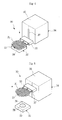
- FIG. 1 is a simplified perspective view of a wafer backside inspection apparatus in accordance with one embodiment of the present invention
- FIG. 2 is a simplified flow diagram useful for explaining a wafer backside inspection method in accordance with another embodiment of the present invention, which may be used with, for example, the apparatus as shown in FIG. 1 ;
- FIG. 3 is a simplified perspective view showing an example of a wafer transfer arm for use in an inspection apparatus and illustrating an exemplary operation of wafer transfer;
- FIGS. 4 to 7 are simplified perspective views showing an example of a wafer flip/aligner for use in an inspection apparatus and illustrating an exemplary operation for flipping a wafer;
- FIG. 8 is a simplified plan view showing an example of an alignment operation for the wafer flip/aligner.
- FIG. 9 is a simplified perspective view showing an example of a wafer inspecting unit for use in an inspection apparatus.
- FIG. 1 is a simplified perspective view of a wafer backside inspection apparatus in accordance with one exemplary embodiment of the present invention.
- wafer backside inspection apparatus 100 comprises wafer cassette 10 , wafer transfer arm 20 , wafer flip/aligner 30 , wafer inspecting unit 40 , wafer buffer stage 50 and defective wafer cassette 60 assembled together on an equipment frame or support structure 110 .
- wafer cassette 10 and defective wafer cassette 60 may be located side-by-side near one side of wafer transfer arm 20 .
- Wafer flip/aligner 30 and wafer inspecting unit 40 may by disposed side-by-side on the opposite side of wafer transfer arm 20 .
- Wafer cassette 10 and defective wafer cassette 60 may be supported by and fixed on respective cassette support tables 70 .
- Wafer transfer arm 20 may be operable to transfer a wafer to a desired position by using vertical, horizontal and revolving movements.
- the various components of the inspecting apparatus 100 may be located close enough to each other on support structure 110 and to wafer transfer arm 20 so as to enable serviceability by wafer transfer arm 20 .
- the elements are an equal distance from the transfer arm.
- Wafer cassette 10 may contain a plurality of wafers, e.g., that may have already been processed by a given wafer fabrication process.
- the wafers may be loaded into different slots of wafer cassette 10 and with their active surfaces facing upwardly.
- the wafers that have been determined to pass a backside inspection may be returned to wafer cassette 10 .
- wafer transfer arm 20 may retrieve a wafer from cassette 10 and may transfer the wafer to a table of flip/aligner 30 .
- Flip/aligner 30 may then flip and align wafer 12 as transferred thereto.
- wafer flip/aligner 30 comprises wafer table 32 and rotator 34 .
- Wafer table 32 may support and fix wafer 12 by use of a vacuum force.
- Rotator 34 may be operable to flip wafer 12 and then place it back on wafer table 32 .
- Wafer table 32 may comprise table body 39 , rotary plate 36 and a sensor ( 38 of FIG. 5 ).
- plate 36 may protrude the top of table body 39 and comprise a diameter smaller than that of the wafer 12 to be placed thereon.
- Rotary plate 36 may apply a vacuum force to the wafer for fixing the wafer thereto and to enable rotation to a predetermined position.
- Sensor 38 may be positioned outside rotary plate 36 and on top of table body 39 for examining the periphery of wafer 12 as will be described subsequently herein.
- rotator 34 may comprise gripper 31 to grip the wafer placed on rotary plate 36 . The rotator may then displace the wafer 12 upwardly from table 32 and may then turn over the wafer 12 .
- rotator 34 comprises a gripper 31 , inverting arm 33 and moving guide 35 .
- Moving guide 35 may comprise an elongated guide hole through which inverting arm 33 may be vertically directed.
- Inverting arm 33 may comprise one end that is connected to moving guide 35 through guide hole 37 . Another end may hold gripper 31 .
- gripper 31 may comprise a pair of jaws—e.g., disposed as a bisected ring.
- the gripper may spread or close-down its jaws to receive and grip a wafer. That is, when wafer 12 is placed on rotary plate 36 of wafer table 32 , gripper 31 may move downwardly along moving guide 35 with its jaws spread outward to allow receipt of the wafer. The jaws may then close-down to grip the periphery of the wafer. While gripping the wafer, gripper 31 may then move upwardly as directed by, e.g., a slot 37 of moving guide 35 . Moving arm 33 may continue moving upwardly to a predetermined height over the table to a position higher than a rotation radius of gripper 31 .
- inverting arm 33 may rotate wafer 12 to an upside down position.
- gripper 31 may move downwardly along moving guide 25 and may return wafer 12 to rotary plate 36 .
- Rotary plate 36 may support wafer 12 and may secure the wafer thereto by a vacuum force.
- a rotor may then spin rotational plate 36 to rotate wafer 12 until sensor 38 detects a flat zone or a notch in a periphery of the wafer. Responsive to such detection by the sensor, rotational plate 36 may then fix its position for an alignment of wafer 12 .
- wafer inspecting unit 40 may inspect the upwardly facing backside surface.
- Wafer inspecting unit 40 in this embodiment, includes wafer stage 42 and vision module 44 .
- Wafer stage 42 may support wafer 12 and secure the wafer thereto with a vacuum force. Additionally, the stage may be further operable to move wafer 12 in any direction along rails 46 . This free movement of wafer 12 by rails 46 may permit vision module 44 to scan and inspect the entire backside of wafer 12 .
- Vision module 44 comprises an inspecting camera 41 that may have its line of sight tilted or directed at an angle relative to the upwardly facing backside surface of wafer 12 on wafer stage 42 .
- a focus camera (not shown) may be located adjacent to the inspecting camera 41 and may be used to assist focusing of inspecting camera 41 .
- monitor camera 45 may be located between inspecting camera 41 and the focusing camera for monitoring the backside of the wafer 12 being inspected.
- Image information from inspecting camera 41 may be transmitted to a controller (not shown) of apparatus 100 . The controller may then analyze the transmitted image information to determine any contamination, cracks or scratches of the wafer backside for identifying, e.g., a pass or failure condition of wafer 12 .
- wafer buffer stage 50 may temporarily hold the wafer before the inspected wafer is re-flipped by wafer flip/aligner 30 .
- Wafer buffer stage 50 thus, may allow continuous and simultaneous inspection processes for several wafers in a parallel or pipelined fashion, as will be explained more fully subsequently herein.
- the wafer when a wafer passes a backside inspection, the wafer may be reloaded into a slot of wafer cassette 10 . Conversely, if a wafer fails an inspection, the wafer may be loaded into a defective wafer cassette 60 .
- Such defective wafer cassette 60 may have a structure that is the same as that of wafer cassette 10 .
- wafers passing the inspection may be loaded into a new wafer cassette instead of being reloaded into the existing cassette 10 .
- FIG. 2 An exemplary method for wafer backside inspection, which may employ apparatus 100 of FIG. 1 , is now described below with reference to FIG. 2 .
- continuous and simultaneous inspection processes of the present embodiment may be described with reference to sequential wafers, for example, a first wafer, of a second wafer and a third wafer.
- a method of wafer backside inspection may begin with providing 81 a wafer cassette 10 having a plurality of wafers. Such wafers may have been treated or processed through previous fabrication processes and loaded into, e.g., respective slots of wafer cassette 10 and contained therein with their active surfaces facing upwardly. As used herein, the non-active surface of the wafers opposite the active surface may be described as the “backside” surface.
- first wafer 12 may be transferred ( 82 of FIG. 2 ) to wafer flip/aligner 30 (FIG. 3 ).
- wafer transfer arm 20 may retrieve (or unload) the first wafer from wafer cassette 10 and then placed the first wafer onto wafer table 32 of wafer flip/aligner 30 .
- first wafer 12 is flipped ( 83 of FIG. 2 ).
- gripper 31 may move down along moving guide 35 of rotator 34 and may close its jaws to grip the periphery of first wafer 12 .
- the gripper may move upwardly along moving guide 35 to a predetermined height above table 32 .
- Inverting arm 33 may then rotate gripper 31 and turn-over wafer 12 such that the backside of first wafer 12 faces upwardly.
- the gripper may move downwardly along moving guide 35 and then place first wafer 12 onto wafer table 32 . After releasing the wafer 12 , gripper 31 may then be returned to its original position.
- first wafer 12 may be aligned ( 84 of FIG. 2 ). With the overturned first wafer 12 on rotary plate 36 of wafer table 32 , first wafer 12 may be fixed thereto by use of, e.g. a vacuum force. Rotary plate 36 may then rotate the first wafer 12 until sensor 38 identifies, e.g., a flat zone or notch 14 . Upon identifying such marking of wafer 12 , sensor 38 may signal the rotational plate 36 to fix its position. Accordingly, wafer 12 may be arranged to a predetermined alignment or radial position. Conventional eight-inch or smaller wafers may have a flat zone formed at a given side along their periphery.
- the wafers may comprise other markings, e.g., such as a notch formed along a periphery thereof.
- the wafers in this embodiment may be further described herein (as illustrated in FIG. 8 ) as comprising notch 14 .
- first wafer 12 may then be sent to a backside inspection ( 85 of FIG. 2 ).
- First wafer 12 may be transferred from wafer table 32 to wafer stage 42 of wafer inspecting unit 40 (e.g., by wafer transfer arm 20 ).
- Wafer stage 42 may support and fix first wafer 12 thereto using, e.g., a vacuum force.
- Rails 46 may guide movement of wafer stage 42 in all directions (e.g., internal and longitudinal directions) along a horizontal plane.
- Vision module 44 may transmit to the controller image information of the surface (i.e., upwardly facing backside) of first wafer 12 .
- the controller may analyze the image information for determination or detection of possible contamination, cracks, scratches and the like which may be present on the backside of first wafer 12 . Subsequently, first wafer 12 may be classified or determined have to passed or failed the inspection based on the analysis of the image information.
- a second wafer may be retrieved from wafer cassette 10 and transferred by wafer transfer arm 20 to wafer flip/aligner 30 .
- the second wafer may then undergo similar flipping and aligning operations by the flip/aligner. After being flipped and aligned, the second wafer may then remain seated at the table of the wafer flip/aligner 30 pending availability of the inspection unit. That is, while the backside of first wafer 12 is being inspected, the second wafer may be flipped and aligned.
- Such processes thus, may be termed continuous and simultaneous for respective individual wafers. That is the flipping and aligning operations can be performed (in pipeline fashion) on the second wafer during the backside inspection of the first wafer.
- Such parallel procedures may allow great efficiency and utilization of inspection apparatus 100 during wafer backside inspections.
- the backside inspection of the first wafer might normally require between 1 and 2 minutes, (although the precision of the inspection may make a little difference). At the same time, it may require between a few and ten-odd seconds to transfer a wafer from wafer cassette 10 to wafer flip/aligner 30 and to align the wafer. Thus, these processes may be performed simultaneously and in parallel.
- the inspected first wafer may be transferred ( 87 of FIG. 2 ) to the wafer buffer stage 50 , e.g., by the wafer transfer arm 20 . Additionally, the second wafer may be transferred from the wafer flip/aligner 30 to wafer inspecting unit 40 .
- first wafer 12 may be transferred from wafer buffer stage 50 to wafer flip/aligner 30 and may then be re-flipped ( 89 of FIG. 2 ). Additionally, the first wafer may be sorted ( 89 of FIG. 2 ) according to results of its backside inspection. Upon sorting the first wafer, a third wafer may be transferred ( 90 of FIG. 2 ) from wafer cassette 10 to the wafer flip/aligner 30 and then flipped and aligned.
- the backside of the first wafer 12 faces upwardly upon completing its backside inspection. Accordingly, the first wafer may be re-flipped just before the sorting so that its front side may face upwardly at its conclusion.
- the re-flipping may be understood to follow procedures similar to the flipping procedures described earlier herein with reference to FIGS. 4 and 7 .
- first wafer 12 if first wafer 12 is determined to pass, then it may be loaded into wafer cassette 10 . In case of determining a failure, the first wafer may be loaded into the defective wafer cassette 60 . The third wafer may then be transferred to the wafer flip/aligner 30 to undergo flipping and alignment. After being flipped and aligned at the wafer flip/aligner 30 , the third wafer may wait for the availability of next procedure pending transfer of the second wafer to wafer buffer stage 50 . Again, the backside inspection may require between 1 and 2 minutes, whereas the re-flipping and sorting of the first wafer 12 and the flipping and aligning of the third wafer may require only a few seconds. Therefore, the re-flipping and sorting of the first wafer and the flipping and aligning of the third wafer might both be performed during the backside inspection of the second wafer.
- the re-flipping and sorting of the Nth wafer and the flipping and aligning of (N+2)th wafer may similarly be performed during the backside inspection of (N+1)th wafer by the wafer inspection unit 40 (N: natural number). Accordingly, the process may be described as continuous and simultaneous for respective individual wafers.
- the Nth wafer may be understood to reference the wafer being re-flipped and sorted; the (N+1)th wafer may be understood to correspond to the wafer undergoing backside inspection in the inspection unit; and the (N+2)th wafer may be understood to correspond to the wafer being flipped and aligned just preceding the inspection.
- wafer buffer stage 50 may be simply a stage where an inspected wafer may wait for the availability of its next procedure. Nonetheless, it may be viewed as enabling performance of the various steps of inspection in a continuous manner as disclosed in exemplary embodiments of the present invention. Without wafer buffer stage 50 , certain steps might not be available for performance in efficient parallel fashion. For example, the next wafer might not be able to be retrieved, flipped and aligned until after completing the sorting of the first wafer.
- transfer of the second wafer to wafer flip/aligner 30 would prevent re-flipping and sorting of the inspected first wafer; the second wafer at wafer flip/aligner 30 would then interfere with re-flipping of the first inspected wafer.
Landscapes
- Physics & Mathematics (AREA)
- Health & Medical Sciences (AREA)
- Life Sciences & Earth Sciences (AREA)
- Chemical & Material Sciences (AREA)
- Analytical Chemistry (AREA)
- Biochemistry (AREA)
- General Health & Medical Sciences (AREA)
- General Physics & Mathematics (AREA)
- Immunology (AREA)
- Pathology (AREA)
- Engineering & Computer Science (AREA)
- Manufacturing & Machinery (AREA)
- Computer Hardware Design (AREA)
- Microelectronics & Electronic Packaging (AREA)
- Power Engineering (AREA)
- Testing Or Measuring Of Semiconductors Or The Like (AREA)
- Container, Conveyance, Adherence, Positioning, Of Wafer (AREA)
- Investigating Materials By The Use Of Optical Means Adapted For Particular Applications (AREA)
Applications Claiming Priority (2)
| Application Number | Priority Date | Filing Date | Title |
|---|---|---|---|
| KR10-2002-0009878A KR100445457B1 (ko) | 2002-02-25 | 2002-02-25 | 웨이퍼 후면 검사 장치 및 검사 방법 |
| KR2002-9878 | 2002-02-25 |
Publications (2)
| Publication Number | Publication Date |
|---|---|
| US20030159528A1 US20030159528A1 (en) | 2003-08-28 |
| US6923077B2 true US6923077B2 (en) | 2005-08-02 |
Family
ID=27751940
Family Applications (1)
| Application Number | Title | Priority Date | Filing Date |
|---|---|---|---|
| US10/283,681 Expired - Fee Related US6923077B2 (en) | 2002-02-25 | 2002-10-29 | Apparatus and method for wafer backside inspection |
Country Status (4)
| Country | Link |
|---|---|
| US (1) | US6923077B2 (ko) |
| JP (1) | JP4343546B2 (ko) |
| KR (1) | KR100445457B1 (ko) |
| DE (1) | DE10304174A1 (ko) |
Cited By (2)
| Publication number | Priority date | Publication date | Assignee | Title |
|---|---|---|---|---|
| US20090002720A1 (en) * | 2007-06-27 | 2009-01-01 | Vistec Semiconductor Systems Gmbh | Device for measuring positions of structures on a substrate |
| US20100279439A1 (en) * | 2009-04-29 | 2010-11-04 | Applied Materials, Inc. | Automated substrate handling and film quality inspection in solar cell processing |
Families Citing this family (26)
| Publication number | Priority date | Publication date | Assignee | Title |
|---|---|---|---|---|
| JP5140428B2 (ja) * | 2004-08-23 | 2013-02-06 | ロッコ・システムズ・プライベイト・リミテッド | 集積回路ダイシング装置のチャック用供給機構 |
| US7728965B2 (en) * | 2005-06-06 | 2010-06-01 | Kla-Tencor Technologies Corp. | Systems and methods for inspecting an edge of a specimen |
| SG143079A1 (en) * | 2006-11-14 | 2008-06-27 | Rokko Systems Pte Ltd | Net block assembly |
| KR100846065B1 (ko) * | 2006-12-29 | 2008-07-11 | 주식회사 실트론 | 웨이퍼 검사장치 및 방법 |
| KR101347065B1 (ko) | 2007-12-20 | 2014-01-10 | 주성엔지니어링(주) | 기판 검사 시스템 및 방법, 및 그를 이용한 태양전지제조방법 |
| DE102008002794A1 (de) | 2008-03-06 | 2009-09-10 | Vistec Semiconductor Systems Gmbh | Verfahren und Vorrichtung zur Bestimmung mindestens eines Parameters bei der Handhabung von Wafern |
| WO2009125896A1 (en) * | 2008-04-08 | 2009-10-15 | Semisysco Co., Ltd. | Wafer testing apparatus and processing equipment having the same |
| DE102008044508A1 (de) | 2008-09-09 | 2010-03-18 | Vistec Semiconductor Systems Jena Gmbh | Vorrichtung zum Halten von scheibenförmigen Objekten |
| US8415967B2 (en) * | 2009-07-17 | 2013-04-09 | Chang Sung Ace Co., Ltd. | Wafer inspection apparatus |
| DE102011051335A1 (de) | 2011-06-26 | 2013-01-10 | Roth & Rau Ag | Substrathalteeinrichtung |
| TWI435074B (zh) * | 2011-06-29 | 2014-04-21 | Mpi Corp | 光學檢測裝置與光學檢測方法 |
| CN102915938B (zh) * | 2012-10-08 | 2015-09-30 | 上海华力微电子有限公司 | 一种检测晶背缺陷的装置及方法 |
| DE112014003220T5 (de) * | 2013-07-11 | 2016-04-28 | Kla-Tencor Corporation | Konfigurationen für einen Metrologietisch und Verfahren zum Betreiben des Metrologietisches |
| JP5752827B2 (ja) * | 2014-03-26 | 2015-07-22 | 東京エレクトロン株式会社 | 基板処理システム、基板搬送方法、プログラム及びコンピュータ記憶媒体 |
| US10054482B2 (en) * | 2014-09-22 | 2018-08-21 | Antonio Maccari | Tool for positioning a scanning device |
| KR101669992B1 (ko) * | 2015-02-17 | 2016-10-27 | 기가비스주식회사 | 기판의 양면 검사장치 |
| JP2018128339A (ja) * | 2017-02-08 | 2018-08-16 | 住友化学株式会社 | 半導体ウェハの表面検査装置及び半導体ウェハの表面検査方法 |
| US10770327B2 (en) | 2017-07-28 | 2020-09-08 | Taiwan Semiconductor Manufacturing Co., Ltd. | System and method for correcting non-ideal wafer topography |
| US11908123B2 (en) | 2018-06-29 | 2024-02-20 | Koh Young Technology Inc. | Object inspection apparatus and object inspection method using same |
| CN110534472B (zh) * | 2019-09-06 | 2021-05-25 | 杭州众硅电子科技有限公司 | 一种晶圆传输机械手及其晶圆翻转方法 |
| EP3953745A4 (en) * | 2019-04-11 | 2023-04-26 | Applied Materials, Inc. | MULTILAYER FILM FOR OPTICAL DEVICES |
| JP2021148474A (ja) * | 2020-03-17 | 2021-09-27 | 株式会社Screenホールディングス | 検査装置、検査方法およびワーク搬送装置 |
| KR102480992B1 (ko) * | 2021-02-24 | 2022-12-26 | (주)하이비젼시스템 | 자재 반전 안착 장치 |
| CN113097104B (zh) * | 2021-03-25 | 2022-08-02 | 青岛天仁微纳科技有限责任公司 | 一种方形基片的生产设备及其生产方法 |
| KR102434404B1 (ko) * | 2022-04-05 | 2022-08-18 | 홍문복 | 자동차 클러스터 조립을 위한 옵티컬 본딩 공정 설비 및 이를 이용한 본딩 방법 |
| WO2024091914A1 (en) * | 2022-10-24 | 2024-05-02 | Jabil Inc. | Apparatus, system and method for providing an edge grip substrate flipper |
Citations (15)
| Publication number | Priority date | Publication date | Assignee | Title |
|---|---|---|---|---|
| JPS5932146A (ja) | 1982-08-18 | 1984-02-21 | Nec Corp | 半導体ウエハ−の検査装置 |
| JPS62128134A (ja) | 1985-11-29 | 1987-06-10 | Toshiba Corp | 半導体ウエハの表面検査装置 |
| US5422724A (en) | 1992-05-20 | 1995-06-06 | Applied Materials, Inc. | Multiple-scan method for wafer particle analysis |
| JPH09199560A (ja) | 1996-01-16 | 1997-07-31 | Sumitomo Sitix Corp | 半導体基板表面欠陥の検査方法及びその自動検査装置 |
| US5715052A (en) | 1994-06-02 | 1998-02-03 | Mitsubishi Denki Kabushiki Kaisha | Method of detecting the position and the content of fine foreign matter on substrates and analyzers used therefor |
| JPH1092887A (ja) | 1996-09-18 | 1998-04-10 | Nikon Corp | ウエハ検査装置 |
| KR19980072335A (ko) | 1997-03-04 | 1998-11-05 | 김광호 | 웨이퍼의 표면검사방법 |
| JPH11121577A (ja) | 1997-10-08 | 1999-04-30 | Mecs Corp | 半導体ウェハの検査システム |
| KR20000002566A (ko) | 1998-06-22 | 2000-01-15 | 존카터주니어 | 서미스터 전극 공급용 호퍼 구조 |
| KR20000001487A (ko) | 1998-06-11 | 2000-01-15 | 윤종용 | 고열방출 특성을 갖는 비지에이 패키지 |
| KR20000007478A (ko) | 1998-07-03 | 2000-02-07 | 이봉훈 | 무선호출 맞춤정보시스템 |
| JP2000097671A (ja) | 1998-09-28 | 2000-04-07 | Olympus Optical Co Ltd | プリント基板の外観検査装置及び外観検査方法 |
| KR20000025668A (ko) | 1998-10-13 | 2000-05-06 | 윤종용 | 정전기 척의 파티클 평가방법과 세정 케미컬처리 전사영향 평가방법 |
| JP2000156391A (ja) | 1998-11-19 | 2000-06-06 | Sony Corp | 半導体ウェーハ検査装置 |
| KR20010033886A (ko) | 1998-11-30 | 2001-04-25 | 기시모토 마사도시 | 웨이퍼검사장치 및 웨이퍼검사방법 |
Family Cites Families (2)
| Publication number | Priority date | Publication date | Assignee | Title |
|---|---|---|---|---|
| JP3791698B2 (ja) * | 1994-09-30 | 2006-06-28 | オリンパス株式会社 | ウエハ検査装置 |
| KR200198268Y1 (ko) * | 1995-06-15 | 2000-12-01 | 김영환 | 웨이퍼 검사장치 |
-
2002
- 2002-02-25 KR KR10-2002-0009878A patent/KR100445457B1/ko not_active IP Right Cessation
- 2002-10-29 US US10/283,681 patent/US6923077B2/en not_active Expired - Fee Related
-
2003
- 2003-01-29 DE DE10304174A patent/DE10304174A1/de not_active Ceased
- 2003-02-18 JP JP2003039718A patent/JP4343546B2/ja not_active Expired - Fee Related
Patent Citations (15)
| Publication number | Priority date | Publication date | Assignee | Title |
|---|---|---|---|---|
| JPS5932146A (ja) | 1982-08-18 | 1984-02-21 | Nec Corp | 半導体ウエハ−の検査装置 |
| JPS62128134A (ja) | 1985-11-29 | 1987-06-10 | Toshiba Corp | 半導体ウエハの表面検査装置 |
| US5422724A (en) | 1992-05-20 | 1995-06-06 | Applied Materials, Inc. | Multiple-scan method for wafer particle analysis |
| US5715052A (en) | 1994-06-02 | 1998-02-03 | Mitsubishi Denki Kabushiki Kaisha | Method of detecting the position and the content of fine foreign matter on substrates and analyzers used therefor |
| JPH09199560A (ja) | 1996-01-16 | 1997-07-31 | Sumitomo Sitix Corp | 半導体基板表面欠陥の検査方法及びその自動検査装置 |
| JPH1092887A (ja) | 1996-09-18 | 1998-04-10 | Nikon Corp | ウエハ検査装置 |
| KR19980072335A (ko) | 1997-03-04 | 1998-11-05 | 김광호 | 웨이퍼의 표면검사방법 |
| JPH11121577A (ja) | 1997-10-08 | 1999-04-30 | Mecs Corp | 半導体ウェハの検査システム |
| KR20000001487A (ko) | 1998-06-11 | 2000-01-15 | 윤종용 | 고열방출 특성을 갖는 비지에이 패키지 |
| KR20000002566A (ko) | 1998-06-22 | 2000-01-15 | 존카터주니어 | 서미스터 전극 공급용 호퍼 구조 |
| KR20000007478A (ko) | 1998-07-03 | 2000-02-07 | 이봉훈 | 무선호출 맞춤정보시스템 |
| JP2000097671A (ja) | 1998-09-28 | 2000-04-07 | Olympus Optical Co Ltd | プリント基板の外観検査装置及び外観検査方法 |
| KR20000025668A (ko) | 1998-10-13 | 2000-05-06 | 윤종용 | 정전기 척의 파티클 평가방법과 세정 케미컬처리 전사영향 평가방법 |
| JP2000156391A (ja) | 1998-11-19 | 2000-06-06 | Sony Corp | 半導体ウェーハ検査装置 |
| KR20010033886A (ko) | 1998-11-30 | 2001-04-25 | 기시모토 마사도시 | 웨이퍼검사장치 및 웨이퍼검사방법 |
Non-Patent Citations (17)
| Title |
|---|
| 102000025668, Samsung Elect., May 6, 2000, English language abstract. |
| 11-121577, MECS Corp., Apr. 30, 1999, English language abstract. |
| 20-0198268, Hyundai , Jul. 21, 2000, English language abstract. |
| 59-032146, NEC Corp., Feb. 21, 1984, English language abstract. |
| English language abstract of Japanese Patent No. 11-121577. |
| English language abstract of Japanese Patent No. 59-032146. |
| English language abstract of Japanese Publication No. 09-199560. |
| English language abstract of Japanese Publication No. 10-092887. |
| English language abstract of Japanese Publication No. 2000-097671. |
| English language abstract of Japanese Publication No. 2000-156391. |
| English language abstract of Japanese Publication No. 62-128134. |
| English language abstract of Korean Patent No. 1020000025668. |
| English language abstract of Korean Publication No. 1020000014876. |
| English language abstract of Korean Publication No. 1020000074786. |
| English language abstract of Korean Publication No. 1998-072335. |
| English language abstract of Korean Publication No. 2001-0033886. |
| English language abstract of Korean Utility Mode No. 20-0198268. |
Cited By (4)
| Publication number | Priority date | Publication date | Assignee | Title |
|---|---|---|---|---|
| US20090002720A1 (en) * | 2007-06-27 | 2009-01-01 | Vistec Semiconductor Systems Gmbh | Device for measuring positions of structures on a substrate |
| US7817262B2 (en) | 2007-06-27 | 2010-10-19 | Vistec Semiconductor Systems Gmbh | Device for measuring positions of structures on a substrate |
| US20100279439A1 (en) * | 2009-04-29 | 2010-11-04 | Applied Materials, Inc. | Automated substrate handling and film quality inspection in solar cell processing |
| US8318512B2 (en) | 2009-04-29 | 2012-11-27 | Applied Materials, Inc. | Automated substrate handling and film quality inspection in solar cell processing |
Also Published As
| Publication number | Publication date |
|---|---|
| DE10304174A1 (de) | 2003-09-11 |
| US20030159528A1 (en) | 2003-08-28 |
| JP4343546B2 (ja) | 2009-10-14 |
| JP2003309155A (ja) | 2003-10-31 |
| KR100445457B1 (ko) | 2004-08-21 |
| KR20030070360A (ko) | 2003-08-30 |
Similar Documents
| Publication | Publication Date | Title |
|---|---|---|
| US6923077B2 (en) | Apparatus and method for wafer backside inspection | |
| CA2259659C (en) | Automatic semiconductor wafer sorter/prober with extended optical inspection | |
| US6559938B1 (en) | Backside contamination inspection device | |
| US4881863A (en) | Apparatus for inspecting wafers | |
| US5706201A (en) | Software to determine the position of the center of a wafer | |
| US4995063A (en) | Single crystal orientation identifying and determining apparatus for semiconductor wafer and its operation method | |
| JPH02236149A (ja) | 印刷回路検査システム | |
| JP2008128651A (ja) | パターン位置合わせ方法、パターン検査装置及びパターン検査システム | |
| WO1998001745A9 (en) | Automatic semiconductor wafer sorter/prober with extended optical inspection | |
| CN101210888A (zh) | 晶片检测机及其方法 | |
| US10937697B2 (en) | Method of processing a semiconductor wafer that involves cutting to form grooves along the dicing lines and grinding reverse side of the wafer | |
| JP2007189211A (ja) | 検査方法および検査装置 | |
| US6401008B1 (en) | Semiconductor wafer review system and method | |
| JPH11121577A (ja) | 半導体ウェハの検査システム | |
| TW202320202A (zh) | 使用斜角晶圓工作台及斜角轉台從晶圓挑揀晶粒之系統和過程 | |
| KR20070002257A (ko) | 웨이퍼 후면 결함 검출 장치 | |
| US7230441B2 (en) | Wafer staging platform for a wafer inspection system | |
| US20070003129A1 (en) | Semiconductor device-inspecting apparatus and semiconductor device-inspecting method | |
| JPH09326426A (ja) | ウェーハの検査装置および方法 | |
| US20230075394A1 (en) | Inspection system | |
| JPS62128134A (ja) | 半導体ウエハの表面検査装置 | |
| JPH05249049A (ja) | 部品の外観検査装置 | |
| JP2004096078A (ja) | アライメント装置 | |
| JPS63127544A (ja) | 半導体製造装置 | |
| JP4913028B2 (ja) | ウエーハ保持装置 |
Legal Events
| Date | Code | Title | Description |
|---|---|---|---|
| AS | Assignment |
Owner name: SAMSUNG ELECTRONICS CO., LTD., KOREA, REPUBLIC OF Free format text: ASSIGNMENT OF ASSIGNORS INTEREST;ASSIGNORS:KIM, DONG-KUK;JEONG, SEUNG-BAE;JEONG, KI-KWON;REEL/FRAME:013442/0463 Effective date: 20020813 |
|
| FEPP | Fee payment procedure |
Free format text: PAYOR NUMBER ASSIGNED (ORIGINAL EVENT CODE: ASPN); ENTITY STATUS OF PATENT OWNER: LARGE ENTITY |
|
| CC | Certificate of correction | ||
| FPAY | Fee payment |
Year of fee payment: 4 |
|
| REMI | Maintenance fee reminder mailed | ||
| LAPS | Lapse for failure to pay maintenance fees | ||
| STCH | Information on status: patent discontinuation |
Free format text: PATENT EXPIRED DUE TO NONPAYMENT OF MAINTENANCE FEES UNDER 37 CFR 1.362 |
|
| FP | Lapsed due to failure to pay maintenance fee |
Effective date: 20130802 |