US6829152B2 - Load drive circuit using flywheel diode - Google Patents
Load drive circuit using flywheel diode Download PDFInfo
- Publication number
- US6829152B2 US6829152B2 US10/310,967 US31096702A US6829152B2 US 6829152 B2 US6829152 B2 US 6829152B2 US 31096702 A US31096702 A US 31096702A US 6829152 B2 US6829152 B2 US 6829152B2
- Authority
- US
- United States
- Prior art keywords
- gate
- mos transistor
- capacitor
- cgd
- capacitance
- Prior art date
- Legal status (The legal status is an assumption and is not a legal conclusion. Google has not performed a legal analysis and makes no representation as to the accuracy of the status listed.)
- Expired - Lifetime
Links
- 239000003990 capacitor Substances 0.000 claims abstract description 98
- 238000011084 recovery Methods 0.000 claims abstract description 71
- 230000001939 inductive effect Effects 0.000 claims abstract description 30
- 238000010992 reflux Methods 0.000 claims abstract description 14
- 239000010410 layer Substances 0.000 claims description 35
- 239000000758 substrate Substances 0.000 claims description 34
- 238000009792 diffusion process Methods 0.000 claims description 31
- 239000012535 impurity Substances 0.000 claims description 31
- 239000004065 semiconductor Substances 0.000 claims description 12
- 229910052751 metal Inorganic materials 0.000 claims description 10
- 239000002184 metal Substances 0.000 claims description 10
- 239000002344 surface layer Substances 0.000 claims description 9
- 230000010355 oscillation Effects 0.000 description 11
- 229910021420 polycrystalline silicon Inorganic materials 0.000 description 9
- 229920005591 polysilicon Polymers 0.000 description 9
- 230000007423 decrease Effects 0.000 description 8
- 230000004048 modification Effects 0.000 description 8
- 238000012986 modification Methods 0.000 description 8
- 238000000034 method Methods 0.000 description 7
- 238000010586 diagram Methods 0.000 description 6
- 230000002093 peripheral effect Effects 0.000 description 6
- 239000000969 carrier Substances 0.000 description 5
- 229920001296 polysiloxane Polymers 0.000 description 4
- 230000000052 comparative effect Effects 0.000 description 3
- 230000008602 contraction Effects 0.000 description 3
- 238000004519 manufacturing process Methods 0.000 description 3
- 238000005457 optimization Methods 0.000 description 3
- 230000003071 parasitic effect Effects 0.000 description 3
- 238000010521 absorption reaction Methods 0.000 description 2
- 230000008901 benefit Effects 0.000 description 2
- 238000011156 evaluation Methods 0.000 description 2
- 230000005669 field effect Effects 0.000 description 2
- 229910044991 metal oxide Inorganic materials 0.000 description 2
- 150000004706 metal oxides Chemical class 0.000 description 2
- 230000008569 process Effects 0.000 description 2
- 229910052782 aluminium Inorganic materials 0.000 description 1
- XAGFODPZIPBFFR-UHFFFAOYSA-N aluminium Chemical compound [Al] XAGFODPZIPBFFR-UHFFFAOYSA-N 0.000 description 1
- 230000006399 behavior Effects 0.000 description 1
- 238000007796 conventional method Methods 0.000 description 1
- 238000001816 cooling Methods 0.000 description 1
- 238000001514 detection method Methods 0.000 description 1
- 230000000694 effects Effects 0.000 description 1
- 230000020169 heat generation Effects 0.000 description 1
- 230000008774 maternal effect Effects 0.000 description 1
- 239000011347 resin Substances 0.000 description 1
- 229920005989 resin Polymers 0.000 description 1
- 230000004044 response Effects 0.000 description 1
- 230000000630 rising effect Effects 0.000 description 1
- 230000001629 suppression Effects 0.000 description 1
- 230000007704 transition Effects 0.000 description 1
- 238000012795 verification Methods 0.000 description 1
Images


Classifications
-
- H—ELECTRICITY
- H01—ELECTRIC ELEMENTS
- H01L—SEMICONDUCTOR DEVICES NOT COVERED BY CLASS H10
- H01L29/00—Semiconductor devices specially adapted for rectifying, amplifying, oscillating or switching and having potential barriers; Capacitors or resistors having potential barriers, e.g. a PN-junction depletion layer or carrier concentration layer; Details of semiconductor bodies or of electrodes thereof ; Multistep manufacturing processes therefor
- H01L29/66—Types of semiconductor device ; Multistep manufacturing processes therefor
- H01L29/68—Types of semiconductor device ; Multistep manufacturing processes therefor controllable by only the electric current supplied, or only the electric potential applied, to an electrode which does not carry the current to be rectified, amplified or switched
- H01L29/76—Unipolar devices, e.g. field effect transistors
- H01L29/772—Field effect transistors
- H01L29/78—Field effect transistors with field effect produced by an insulated gate
- H01L29/7801—DMOS transistors, i.e. MISFETs with a channel accommodating body or base region adjoining a drain drift region
- H01L29/7802—Vertical DMOS transistors, i.e. VDMOS transistors
- H01L29/7813—Vertical DMOS transistors, i.e. VDMOS transistors with trench gate electrode, e.g. UMOS transistors
-
- H—ELECTRICITY
- H01—ELECTRIC ELEMENTS
- H01L—SEMICONDUCTOR DEVICES NOT COVERED BY CLASS H10
- H01L29/00—Semiconductor devices specially adapted for rectifying, amplifying, oscillating or switching and having potential barriers; Capacitors or resistors having potential barriers, e.g. a PN-junction depletion layer or carrier concentration layer; Details of semiconductor bodies or of electrodes thereof ; Multistep manufacturing processes therefor
- H01L29/66—Types of semiconductor device ; Multistep manufacturing processes therefor
- H01L29/68—Types of semiconductor device ; Multistep manufacturing processes therefor controllable by only the electric current supplied, or only the electric potential applied, to an electrode which does not carry the current to be rectified, amplified or switched
- H01L29/76—Unipolar devices, e.g. field effect transistors
- H01L29/772—Field effect transistors
- H01L29/78—Field effect transistors with field effect produced by an insulated gate
- H01L29/7801—DMOS transistors, i.e. MISFETs with a channel accommodating body or base region adjoining a drain drift region
- H01L29/7802—Vertical DMOS transistors, i.e. VDMOS transistors
- H01L29/7803—Vertical DMOS transistors, i.e. VDMOS transistors structurally associated with at least one other device
- H01L29/7804—Vertical DMOS transistors, i.e. VDMOS transistors structurally associated with at least one other device the other device being a pn-junction diode
- H01L29/7805—Vertical DMOS transistors, i.e. VDMOS transistors structurally associated with at least one other device the other device being a pn-junction diode in antiparallel, e.g. freewheel diode
-
- H—ELECTRICITY
- H01—ELECTRIC ELEMENTS
- H01L—SEMICONDUCTOR DEVICES NOT COVERED BY CLASS H10
- H01L29/00—Semiconductor devices specially adapted for rectifying, amplifying, oscillating or switching and having potential barriers; Capacitors or resistors having potential barriers, e.g. a PN-junction depletion layer or carrier concentration layer; Details of semiconductor bodies or of electrodes thereof ; Multistep manufacturing processes therefor
- H01L29/66—Types of semiconductor device ; Multistep manufacturing processes therefor
- H01L29/68—Types of semiconductor device ; Multistep manufacturing processes therefor controllable by only the electric current supplied, or only the electric potential applied, to an electrode which does not carry the current to be rectified, amplified or switched
- H01L29/76—Unipolar devices, e.g. field effect transistors
- H01L29/772—Field effect transistors
- H01L29/78—Field effect transistors with field effect produced by an insulated gate
- H01L29/7801—DMOS transistors, i.e. MISFETs with a channel accommodating body or base region adjoining a drain drift region
- H01L29/7802—Vertical DMOS transistors, i.e. VDMOS transistors
- H01L29/7811—Vertical DMOS transistors, i.e. VDMOS transistors with an edge termination structure
-
- H—ELECTRICITY
- H02—GENERATION; CONVERSION OR DISTRIBUTION OF ELECTRIC POWER
- H02M—APPARATUS FOR CONVERSION BETWEEN AC AND AC, BETWEEN AC AND DC, OR BETWEEN DC AND DC, AND FOR USE WITH MAINS OR SIMILAR POWER SUPPLY SYSTEMS; CONVERSION OF DC OR AC INPUT POWER INTO SURGE OUTPUT POWER; CONTROL OR REGULATION THEREOF
- H02M1/00—Details of apparatus for conversion
- H02M1/08—Circuits specially adapted for the generation of control voltages for semiconductor devices incorporated in static converters
-
- H—ELECTRICITY
- H01—ELECTRIC ELEMENTS
- H01L—SEMICONDUCTOR DEVICES NOT COVERED BY CLASS H10
- H01L2224/00—Indexing scheme for arrangements for connecting or disconnecting semiconductor or solid-state bodies and methods related thereto as covered by H01L24/00
- H01L2224/01—Means for bonding being attached to, or being formed on, the surface to be connected, e.g. chip-to-package, die-attach, "first-level" interconnects; Manufacturing methods related thereto
- H01L2224/42—Wire connectors; Manufacturing methods related thereto
- H01L2224/47—Structure, shape, material or disposition of the wire connectors after the connecting process
- H01L2224/48—Structure, shape, material or disposition of the wire connectors after the connecting process of an individual wire connector
- H01L2224/4805—Shape
- H01L2224/4809—Loop shape
- H01L2224/48091—Arched
-
- H—ELECTRICITY
- H01—ELECTRIC ELEMENTS
- H01L—SEMICONDUCTOR DEVICES NOT COVERED BY CLASS H10
- H01L2224/00—Indexing scheme for arrangements for connecting or disconnecting semiconductor or solid-state bodies and methods related thereto as covered by H01L24/00
- H01L2224/01—Means for bonding being attached to, or being formed on, the surface to be connected, e.g. chip-to-package, die-attach, "first-level" interconnects; Manufacturing methods related thereto
- H01L2224/42—Wire connectors; Manufacturing methods related thereto
- H01L2224/47—Structure, shape, material or disposition of the wire connectors after the connecting process
- H01L2224/48—Structure, shape, material or disposition of the wire connectors after the connecting process of an individual wire connector
- H01L2224/484—Connecting portions
- H01L2224/4847—Connecting portions the connecting portion on the bonding area of the semiconductor or solid-state body being a wedge bond
- H01L2224/48472—Connecting portions the connecting portion on the bonding area of the semiconductor or solid-state body being a wedge bond the other connecting portion not on the bonding area also being a wedge bond, i.e. wedge-to-wedge
-
- H—ELECTRICITY
- H01—ELECTRIC ELEMENTS
- H01L—SEMICONDUCTOR DEVICES NOT COVERED BY CLASS H10
- H01L2224/00—Indexing scheme for arrangements for connecting or disconnecting semiconductor or solid-state bodies and methods related thereto as covered by H01L24/00
- H01L2224/01—Means for bonding being attached to, or being formed on, the surface to be connected, e.g. chip-to-package, die-attach, "first-level" interconnects; Manufacturing methods related thereto
- H01L2224/42—Wire connectors; Manufacturing methods related thereto
- H01L2224/47—Structure, shape, material or disposition of the wire connectors after the connecting process
- H01L2224/49—Structure, shape, material or disposition of the wire connectors after the connecting process of a plurality of wire connectors
- H01L2224/491—Disposition
- H01L2224/4912—Layout
- H01L2224/49175—Parallel arrangements
-
- H—ELECTRICITY
- H01—ELECTRIC ELEMENTS
- H01L—SEMICONDUCTOR DEVICES NOT COVERED BY CLASS H10
- H01L29/00—Semiconductor devices specially adapted for rectifying, amplifying, oscillating or switching and having potential barriers; Capacitors or resistors having potential barriers, e.g. a PN-junction depletion layer or carrier concentration layer; Details of semiconductor bodies or of electrodes thereof ; Multistep manufacturing processes therefor
- H01L29/02—Semiconductor bodies ; Multistep manufacturing processes therefor
- H01L29/06—Semiconductor bodies ; Multistep manufacturing processes therefor characterised by their shape; characterised by the shapes, relative sizes, or dispositions of the semiconductor regions ; characterised by the concentration or distribution of impurities within semiconductor regions
- H01L29/0603—Semiconductor bodies ; Multistep manufacturing processes therefor characterised by their shape; characterised by the shapes, relative sizes, or dispositions of the semiconductor regions ; characterised by the concentration or distribution of impurities within semiconductor regions characterised by particular constructional design considerations, e.g. for preventing surface leakage, for controlling electric field concentration or for internal isolations regions
- H01L29/0607—Semiconductor bodies ; Multistep manufacturing processes therefor characterised by their shape; characterised by the shapes, relative sizes, or dispositions of the semiconductor regions ; characterised by the concentration or distribution of impurities within semiconductor regions characterised by particular constructional design considerations, e.g. for preventing surface leakage, for controlling electric field concentration or for internal isolations regions for preventing surface leakage or controlling electric field concentration
- H01L29/0638—Semiconductor bodies ; Multistep manufacturing processes therefor characterised by their shape; characterised by the shapes, relative sizes, or dispositions of the semiconductor regions ; characterised by the concentration or distribution of impurities within semiconductor regions characterised by particular constructional design considerations, e.g. for preventing surface leakage, for controlling electric field concentration or for internal isolations regions for preventing surface leakage or controlling electric field concentration for preventing surface leakage due to surface inversion layer, e.g. with channel stopper
-
- H—ELECTRICITY
- H01—ELECTRIC ELEMENTS
- H01L—SEMICONDUCTOR DEVICES NOT COVERED BY CLASS H10
- H01L2924/00—Indexing scheme for arrangements or methods for connecting or disconnecting semiconductor or solid-state bodies as covered by H01L24/00
- H01L2924/10—Details of semiconductor or other solid state devices to be connected
- H01L2924/11—Device type
- H01L2924/13—Discrete devices, e.g. 3 terminal devices
- H01L2924/1304—Transistor
- H01L2924/1305—Bipolar Junction Transistor [BJT]
- H01L2924/13055—Insulated gate bipolar transistor [IGBT]
-
- H—ELECTRICITY
- H01—ELECTRIC ELEMENTS
- H01L—SEMICONDUCTOR DEVICES NOT COVERED BY CLASS H10
- H01L2924/00—Indexing scheme for arrangements or methods for connecting or disconnecting semiconductor or solid-state bodies as covered by H01L24/00
- H01L2924/10—Details of semiconductor or other solid state devices to be connected
- H01L2924/11—Device type
- H01L2924/13—Discrete devices, e.g. 3 terminal devices
- H01L2924/1304—Transistor
- H01L2924/1306—Field-effect transistor [FET]
- H01L2924/13091—Metal-Oxide-Semiconductor Field-Effect Transistor [MOSFET]
-
- H—ELECTRICITY
- H01—ELECTRIC ELEMENTS
- H01L—SEMICONDUCTOR DEVICES NOT COVERED BY CLASS H10
- H01L2924/00—Indexing scheme for arrangements or methods for connecting or disconnecting semiconductor or solid-state bodies as covered by H01L24/00
- H01L2924/15—Details of package parts other than the semiconductor or other solid state devices to be connected
- H01L2924/181—Encapsulation
-
- H—ELECTRICITY
- H01—ELECTRIC ELEMENTS
- H01L—SEMICONDUCTOR DEVICES NOT COVERED BY CLASS H10
- H01L2924/00—Indexing scheme for arrangements or methods for connecting or disconnecting semiconductor or solid-state bodies as covered by H01L24/00
- H01L2924/19—Details of hybrid assemblies other than the semiconductor or other solid state devices to be connected
- H01L2924/191—Disposition
- H01L2924/19101—Disposition of discrete passive components
- H01L2924/19105—Disposition of discrete passive components in a side-by-side arrangement on a common die mounting substrate
Definitions
- the present invention relates to a circuit for driving an inductive load, and in particular, to the circuit in which a flywheel diode is used.
- inductive loads such as electric motors
- inverters that require switching elements.
- Power MOSFETs are frequently used as the switching elements.
- the power MOSFET is composed to have the function as a flywheel diode by making use of an internal body diode embedded within the element.
- the body diode embedded in the power MOSFET has generally a poor recovery characteristic (i.e., poor reverse recovery characteristic), thus giving rise to higher recovery surge voltage and an oscillation phenomenon called ringing. In some cases, such undesirable phenomena will lead to element breakage and noise generation. Accordingly, the poor recovery characteristic of the body diode becomes an obstacle to a satisfactory performance of a product in which the power MOSFET is incorporated.
- An object of the present invention is to provide a flywheel diode whose recovery characteristic (i.e., reverse recovery characteristic) is softened (or smoothed) with ease so that recovery surges are suppressed in a well controlled manner.
- recovery characteristic i.e., reverse recovery characteristic
- a reflux closed circuit connected to an inductive load, the circuit comprising: a flywheel diode inserted in the reflux closed circuit; a MOS transistor connected in parallel to the flywheel diode; a capacitor of which both ends are connected to a gate and a drain of the MOS transistor; a resistor of which both ends are connected to the gate and a source of the MOS transistor; and means for controlling a gate-to-source voltage of the MOS transistor by causing both the capacitor and resistor to raise the gate-to-source voltage up to a value over a threshold voltage given the MOS transistor for a predetermined period of time during a recovery operation of the flywheel diode.
- both of the capacitor and the resistor allows a gate-to-source voltage of the MOS transistor to be pulled up over the predetermined threshold for a specified period of time.
- the recovery characteristic of the flywheel diode can be softened (or smoothed), thus recovery surges being suppressed.
- the capacitor is set to satisfy a relationship of Vth ⁇ (Cm+Cgd)/(Cm+Cgd+Cgs) ⁇ Vdd, wherein Vth is a threshold voltage of the MOS transistor, Cm is a capacitance of the capacitor, Cgs is a capacitance between the gate and source of the MOS transistor whose drain is subject to application of a power supply voltage, Cgd is a capacitance between the gate and drain of the MOS transistor whose drain is subject to application of a power supply voltage, and Vdd is a voltage of a power supply.
- Vth is a threshold voltage of the MOS transistor
- Cm is a capacitance of the capacitor
- Cgs is a capacitance between the gate and source of the MOS transistor whose drain is subject to application of a power supply voltage
- Cgd is a capacitance between the gate and drain of the MOS transistor whose drain is subject to application of a power supply voltage
- Vdd is a voltage of a power
- the resistor is set to satisfy a relationship of 1 ⁇ 10 ⁇ 7 ⁇ Rm(Cm+Cgd+Cgs) ⁇ 5 ⁇ 10 ⁇ 6 , wherein Rm is a resistance of the resistor, Cm is a capacitance of the capacitor, Cgs is a capacitance between the gate and source of the MOS transistor whose drain is subject to application of a power supply voltage, and Cgd is a capacitance between the gate and drain of the MOS transistor whose drain is subject to application of a power supply voltage.
- a flywheel diode comprises a first conductive type of semiconductor substrate; a second conductive type of flywheel-diode-forming impurity diffusion region formed in a surface layer part of a first surface; an anode electrode formed on the first surface so as to contact the flywheel-diode-forming impurity diffusion region; and a cathode electrode formed on a second surface of the semiconductor substrate, wherein a first conductive type of region is exposed from the first surface of the semiconductor substrate, a first conductive type of MOS-transistor impurity diffusion region is partly formed in a surface layer part of the flywheel-diode-forming impurity diffusion region, a gate electrode is formed above between the exposed first conductive type of region and the MOS-transistor impurity diffusion region via a gate insulating layer, and the anode electrode is brought into contact with both of the flywheel-diode-forming impurity diffusion region and the MOS-transistor impurpur
- a load drive circuit for driving an inductive load, in which two or more pairs of two power MOS transistors mutually connected in series are connected pair by pair to positive and negative power lines, each MOS transistor including a body diode serving as a flywheel diode, and a line mutually connecting the paired two power MOS transistors are connected to the inductive load, wherein the paired two power MOS transistors are operated by turns by controlling a gate voltage of each power MOS transistor.
- the load drive circuit comprises a capacitor of which both ends are connected to a gate and a drain of each power MOS transistor; a resistor of which both ends are connected to the gate and a source of each power MOS transistor; and means for controlling a gate-to-source voltage of each power MOS transistor by causing both the capacitor and resistor to raise the gate-to-source voltage up to a value over a threshold voltage given the power MOS transistors for a predetermined period of time during a recovery operation of the flywheel diode.
- the recovery characteristic of the flywheel diode can be softened (or smoothed), thus recovery surges being suppressed.
- This load drive circuit can be embodied into various forms.
- an external flywheel diode can be connected to the MOS transistor, not being embedded within the MOS transistor.
- the MOS transistor can be replaced by an IGBT element.
- a chip into which each power MOS transistor is incorporated is mounted on a metal plate.
- the drain of the power MOS transistor is electrically connected to the metal plate through the chip, and both of the metal plate and a gate-lead frame are connected to a chip capacitor composing the capacitor.
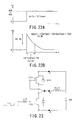
- FIG. 1 shows the configuration of a conventional load drive circuit serving as an inverter
- FIG. 2 shows a conventionally used peripheral circuit of a power MOS transistor
- FIG. 3 is the diagram showing a bridge circuit for the U-phase according to a conventional technique
- FIG. 4 shows timing charts explaining the operations of the conventional bridge circuit
- FIG. 5 is a circuit diagram showing a further conventional load drive circuit
- FIG. 6 shows a cross section of a diode chip used by the conventional load drive circuit
- FIG. 7 shows timing charts explaining the operations of the further conventional load drive circuit
- FIG. 8 is a circuit diagram showing a load drive circuit functioning as an inverter according to a first embodiment of the present invention.
- FIG. 9 is a pictorial illustration showing a cross section of a power MOS transistor incorporated in the load drive circuit
- FIG. 10 represents both the power MOS transistor and its peripheral circuit
- FIG. 11A illustrates the mounting structure of both the power MOS transistor and a capacitor connected thereto
- FIG. 11B outline a section along a A—A line in FIG. 11A;
- FIG. 12 is a diagram showing a bridge circuit for the U-phase
- FIG. 13 shows timing charts explaining the operation of the bridge circuit for the U-phase
- FIG. 14 is a bridge diagram for the U-phase, which was employed to verify an advantage of the bridge circuit according to the embodiment
- FIG. 15 is an equivalent circuit diagram of the power MOS transistor
- FIG. 16 shows graphs obtained by the foregoing verification
- FIG. 17 is a cross section of the power MOS transistor, which is adopted to show the operation thereof;
- FIG. 18 is another cross section of the power MOS transistor, which is adopted to show the operation thereof;
- FIG. 19 is another cross section of the power MOS transistor, which is adopted to show the operation thereof;
- FIG. 20 is another cross section of the power MOS transistor, which is adopted to show the operation thereof;
- FIG. 21 is an illustration for optimization of elements connected to the power MOS transistor
- FIGS. 22A and 22B are timing charts for explaining the optimization of a load drive circuit
- FIG. 23 is a bridge circuit for the U-phase, which is adopted for comparison with that in the present embodiment.
- FIG. 24 shows graphs obtained from the bridge circuit employed for the comparison
- FIG. 25 is a cross section of the power MOS transistor, which is employed to show the operation thereof in a comparative manner
- FIG. 26 is a further cross section of the power MOS transistor, which is employed to show the operation thereof in a comparative manner
- FIG. 27 is a circuit showing a modification of the peripheral circuit of the power MOS transistor
- FIG. 28 is a circuit showing a further modification of the peripheral circuit of the power MOS transistor
- FIG. 29 is the configuration showing a load drive circuit according to a second embodiment of the present invention.
- FIG. 30 shows a cross section of a diode chip used by the load drive circuit
- FIG. 31 shows timing charts explaining the operation of the load drive circuit
- FIG. 32 is a partly shown cross section of a diode chip according to a modification.
- FIG. 1 shows a prior-art three-phase bridge circuit (i.e., an inverter) to drive an AC motor.
- this circuit two power transistors in each of U, V and W phases, that is, a total of six power transistors T 101 to T 106 are provided.
- Each power transistor T 101 (to T 106 ) contains an internal body diode (functioning as a flywheel diode) D 101 (to D 106 ) embedded therein.
- FIG. 2 shows a peripheral circuit connected to the power transistor T 101 , which is representative of the power transistors T 101 to T 106 .
- a control circuit 101 drives the transistor T 101 via a gate drive circuit 100 so that a load is brought into its powered state.
- the control circuit 101 monitors a gate voltage Vg as well, so that the control circuit 101 is able to detect the fact that the gate voltage Vg is less than a predetermined threshold on completion of the activated state. Responsively to this detection, the control circuit 101 turns on a transistor T 113 to short-circuit both a gate terminal and a source terminal of the power transistor T 101 to each other.
- FIG. 3 An assumption can be made as shown in FIG. 3, wherein a load (coil) is current-supplied by making two transistors T 101 and T 102 turn on and turn off, by turns.
- a gate signal SG 1 to the first transistor T 101 a gate signal SG 2 to the second transistor T 102 , gate voltages Vg 1 and Vg 2 to both the transistors T 101 and T 102 respectively, a drain-to-source voltage Vds 1 of the first transistor T 101 , a drain voltage Vd 2 of the second transistor T 102 , a current If flowing through a flywheel diode D 101 connected in parallel to the first transistor T 101 , and a current Id 2 flowing through the second transistor T 102 can be shown in their behaviors by FIG. 4 .
- references t 100 and t 104 are turn-off command timings assigned to the first transistor T 101 , while a reference t 103 is a turn-on command timing assigned thereto. Also references t 101 and t 105 are turn-on command timings assigned to the second transistor T 102 , while a reference t 102 is a turn-off command timing assigned thereto.
- a turn-off operation is commanded to the first transistor T 101 , and then at the timing t 101 , a turn-on operation is commanded to the second transistor T 102 .
- the gate voltage Vg 1 to the first transistor T 101 decreases gradually after the timing t 100
- the gate voltage Vg 2 to the second transistor T 102 rises gradually after the timing t 101
- the current If is reduced after the timing t 101 and the current Id 2 rises after the timing t 101
- the drain voltage Vd 2 of the second transistor T 102 decreases after the timing t 101 .
- a succeeding timing t 200 the current If flowing the diode becomes zero (A), at which the diode transits into its reverse recovery (simply, recovery) process until its reversal caused at a succeeding timing t 201 .
- the flywheel diode When passing the timing t 201 , the flywheel diode acts as a capacitor in the circuit, thus causing an LC oscillation with a parasitic inductance of the circuit (refer to FIG. 28 ).
- the diode current If gradually converges to zero (A).
- the drain-to-source voltage Vds 1 of the first transistor T 101 is also oscillated.
- a gate register (as shown by a reference R 101 in FIG. 2) is adjustably placed or gate control means is improved so that the switching speed is reduced to suppress the surge voltage.
- This way is known as adjustment of the performance of a drive transistor.
- a snubber circuit can be added to suppress the surge voltage and prevent the oscillation.
- it is very difficult to prevent the performance of a product using the drive circuit from being deteriorated, the production cost from increasing, and the size of the product from increasing.
- the generation of a surge voltage and noise is not limited to the case where the inverter is used to control AC motors in a PWM manner. Such generation also occurs during switching operations for PWM-controlling DC motors. This situation will now be described with reference to FIGS. 5 to 7 .
- a DC power supply 150 is provided. Both of a positive terminal and the ground of the DC power supply 150 are connected to a serially connected circuit of a switch 151 , an inductive load (i.e., DC motor) and a power MOS transistor 153 .
- a flywheel diode 154 is embedded in the power MOS transistor 153 .
- a gate terminal of the power MOS transistor 153 is connected with a gate drive circuit 156 via a resistor 155 .
- a further flywheel diode 157 is coupled with the inductive load 152 in parallel.
- the flywheel diode 157 is structured as shown in FIG. 6, where an n-type silicone substrate 160 is produced by forming an n ⁇ epitaxial layer 162 on a n+ silicone substrate 161 . In a surface of the layer 162 positioned opposite to the substrate 160 , a p-type impurity diffused region 163 is locally formed. An anode electrode 164 is formed on the surface of the layer 162 so that the anode electrode 164 is brought into contact with the p-type impurity diffused region 163 . A cathode electrode 165 is formed on an outer surface of the substrate 161 .
- the circuitry in FIG. 5 is driven as shown in a timing chart shown in FIG. 7, in which the power MOS transistor 153 is switched at a high speed responsively to drive the inductive load 152 .
- a surge voltage and noise are generated when the transistor 153 is switched.
- both of a surge voltage known as a recovery surge and an oscillation phenomenon known as ringing are generated.
- Such undesired phenomena will lead to damaging elements and noise generation.
- SG 10 shows a gate signal to the transistor 153
- Vg 10 shows a gate voltage to the transistor 153
- Id shows a current flowing through the transistor 153
- Vd shows a drain voltage of the transistor 153
- V 1 shows a voltage between an anode and cathode of the flywheel diode 157 .
- Such countermeasures include a technique of placing a coil and a capacitor into the drive circuit to compose both a filter circuit and a surge absorption circuit therein and a further technique of making the switching speed of the power MOS transistor slower to suppress surges and noise.
- the latter technique has been taken mainly.
- this technique that is, slowing down the switching speed of the power MOS transistor 153 , will increase switching loss at the transistor 153 , thus generating a larger amount of heat. This heat generation necessitates a larger-size cooling structure, thus making the power MOS transistor 153 larger in its dimensions.
- an inductive-load drive circuit for automobiles which requires a rated voltage of 60 to 100 volts, employs the foregoing countermeasures (in other words, the arrangement of a filter circuit and a surge absorption circuit and the delay control of switching speed of a power MOS transistor). It is therefore inevitable that the inductive-load drive circuit for automobiles will deteriorate in its performance, a rise in the production cost, and an enlargement in its dimensions.
- the present invention has therefore been made to overcome the difficulties faced by the inductive-load drive circuit, which is preferable for automobiles, for instance.
- FIGS. 8 to 26 a first embodiment of the present invention will now be explained.
- FIG. 8 shows the electrical configuration of a thee-phase bridge circuit (inverter) for driving an AC motor in the present embodiment.
- a DC power supply B is placed to provide a positive electrode line (P line) and a negative electrode line (N line), between which a capacitor C is connected.
- a serial circuit composed of power MOS transistors (MOSFETs: metal-oxide semiconductor field-effect transistors) T 1 and T 2 is connected so as to be in parallel with the capacitor C, respectively.
- MOSFETs metal-oxide semiconductor field-effect transistors
- T 5 and T 6 are connected so as to be in parallel with the capacitor C, respectively.
- FIG. 9 shows a section structure of each of the power MOS transistors T 1 to T 6 .
- Each transistor T 1 (to T 6 ) is structured into an n-channel longitudinal MOSFET of trench-gate type. More concretely, an n ⁇ epitaxial layer 21 is formed on an n + semiconductor substrate 20 . In the surface portion of the n ⁇ epitaxial layer 21 , which is opposite to the substrate 20 , a p-well region (p-base region) 22 is formed. Part of the n ⁇ epitaxial layer 21 located beneath the p-base region 22 serves as an n ⁇ drift layer. In the surface portion of the p-base region 22 , which is opposite to the substrate 20 , a large number of n-source regions 23 are formed.
- each trench 24 is formed so as to penetrate into each n-source region and the p-base region 22 and to reach the n ⁇ epitaxial layer 21 .
- a polysilicon gate electrode 26 is formed with a gate oxide (i.e., gate-insulating layer) 25 disposed therebetween.
- Each gate electrode 26 is covered by each insulating layer 27 , on which a source electrode 28 is formed so that the electrode 28 is brought into contact with both part of the p-base region 22 and part of the n-source regions 23 .
- a drain electrode 29 is formed on the back surface of the n + semiconductor substrate 20 .
- a body diode is produced internally, which functions as each of the flywheel diodes Df 1 to Df 6 shown in FIG. 8 .
- each power MOS transistor T 1 to T 6 a capacitor C 1 (to D 6 ) is connected between the train and the gate of each power MOS transistors T 1 to T 6 .
- the gate terminal of each power MOS transistor T 1 (to T 6 ) is coupled with each gate drive circuit 1 (to 6 ) via each resistor R 1 (to R 6 ).
- One end of each resistor R 1 (R 6 ) is also coupled with the source terminal of each power MOS transistor T 1 (to T 6 ) via each diode D 1 (to D 6 ) and each transistor T 11 (to T 16 ).
- the base of each transistor T 11 (to T 16 ) is connected to each gate drive circuit 1 (to 6 ).
- All the gate drive circuits 1 to 6 have the same circuitry, and one gate drive circuit 1 connected to both the U-phase of the inductive load M and the positive electrode (P-line side) of the power supply B.
- the gate drive circuit 1 is equipped with two transistors T 21 and T 22 connected in series with each other, two resistors R 11 and R 12 connected in series with each other, and a diode D 11 connected in parallel with the resistor R 12 .
- the gate terminal of the power MOS transistor T 1 is linked with a given circuit path between the two transistors T 21 and T 22 by way of the three series-connected resistors R 1 , R 12 and R 11 .
- Each of the gate drive circuits 1 to 6 shown in FIG. 8 is connected to a control circuit 10 shown in FIG. 10 .
- the control circuit 10 is connected with the base terminals of the two transistors T 21 and T 22 incorporated in each of the gate drive circuits 1 to 6 .
- the control circuit 10 is also connected to the base terminal of each of the foregoing transistors T 11 to T 16 .
- the control circuit 10 is configured to monitor a gate voltage Vg of each power MOS transistor T 1 (to T 6 ) and to make each corresponding transistor T 11 (to T 16 ) turn on when the gate voltage Vg reaches an amount equal or smaller to or than a given value (practically, for example, 3 volts).
- the control circuit 10 controls each of the power MOS transistors T 1 to T 6 in an on/off manner so that the inductive load M is operated on a PWM (pulse width modulation) basis.
- the control circuit 10 is configured to turn on the transistor T 21 of each gate drive circuit 1 (to 6 ), so that the gate voltage Vg of each power MOS transistor T 1 (to T 6 ) increase so as to make the transistor T 1 (to T 6 ) turn on.
- the transistor T 1 (to T 6 ) is made to be off, thus causing the transistor T 22 to turn on, with the result that the gate voltage Vg is lowered.
- the control circuit 10 is able to make each corresponding transistor T 11 (to T 16 ) turn on. This allows the gate terminal of each power MOS transistor T 1 (to T 6 ) to connect to the source terminal thereof by way of the resistor (R 1 in FIG. 10) and the diode (D 1 in FIG. 10 ).
- each body diode embedded in each power MOS transistor T 1 (to T 6 ) is used as each of the flywheel diodes Df 1 to Df 6 .
- the power MOS transistor T 1 (to T 6 ) operates with its gate terminal connected to its source terminal via the resistor R 1 (in the case of the transistor T 1 ).
- FIGS. 11A and 11B illustrate a structure in which a chip 30 including the power MOS transistor is mounted on a substrate.
- the chip is mounted on a copper-made substrate 31 and the drain electrode of the power MOS transistor is electrically coupled with the copper-made substrate 31 .
- the copper-made substrate 31 functions as a heat sink for the power MOS transistor.
- Bonding wires 33 connect the chip 30 and lead frames 32 .
- a chip capacitor 34 is mounted, which serves as a capacitor C 1 (to C 6 ) to connect the drain terminal and the gate terminal of the power MOS transistor, as shown in FIG. 10 . All the components shown in FIGS. 11A ( 11 B) and are molded with resin maternal 35 .
- FIG. 12 outlines the configuration of a bridge circuit for the U-phase among the U-, V- and W-phases of the inverter.
- N-line side one power MOS transistor
- P-line side the other power MOS transistor
- a gate signal SG 1 to the transistor T 1 a gate signal SG 2 to the transistor T 2 , gate voltages Vg 1 and Vg 2 to the transistors T 1 and T 2 , a voltage Vds 1 between the drain and source of the transistor T 1 , a drain voltage Vd 2 of the transistor T 2 , a current If flowing through the flywheel diode Df 1 at the transistor T 1 , and a current Id 2 flowing through the transistor T 2 can be exemplified as in FIG. 13 .
- references t 1 and t 5 show timings at which the transistor T 1 is commanded to turn off, respectively, while a reference t 4 shows a timing at which the transistor T 1 is commanded to turn on. Furthermore, references t 2 and t 6 show timings at which the transistor T 2 is commanded to turn on, respectively, while a reference t 3 shows a timing at which the transistor T 2 is commanded to turn off.
- a certain reflux current i.e., in this case, transistor current
- a command to turn off the transistor T 1 is issued at the timing t 1
- a command to turn on the transistor T 2 is issued at the timing t 2 .
- the gate voltage Vg 1 decreases immediately after the timing t 1 , so that the reflux current changes from the transistor current to the diode current.
- the gate voltage Vg 2 begins to increase from the timing t 2 .
- the flywheel diode current If begins to descend from the timing t 2 , whilst the drain current Id 2 begins to rise from the timing t 2 . From the timing t 2 , the drain voltage Vd 2 decreases. Then the diode current If becomes zero at a timing t 10 , before entering a recovery process at the diode, during which time the process is reversed at a timing t 11 .
- the circuit composed of the capacitor C 1 and the resistor R 1 shown in FIG. 12 operates to lift the gate-souse voltage Vg 1 above a given threshold voltage during a certain period of time.
- the diode current If is made to converge to zero.
- the recovery characteristic of the diode Df 1 which is in operation under the condition that current flows though the U-phase, with one power MOS transistor T 2 (N-line side) operating as a load-driving transistor and with the other power MOS transistor T 1 (P-line side) functioning as a flywheel diode, was evaluated with the use of an evaluation circuit shown in FIG. 14 .
- the transistor elements T 1 and T 2 were formed into trench gate type of DMOS (double-diffused metal oxide semiconductor) and had a rated voltage of 100 [V], a rated current of 200 [A], and a chip dimension of 11 [mm] by 9 [mm].
- a threshold voltage of each transistor T 1 (T 2 ) was 3.2 [V].
- FIG. 16 shows a diode recovery characteristic of the U-phase P-line transistor T 1 estimated on the circuits shown in FIGS. 7 and 8.
- the lateral axis shows time, while the vertical axis shows a diode current If, source-to-drain voltage Vd, and gate-to-source voltage Vg.
- One scale division along the lateral axis (time axis) is 250 [nsec] (i.e., 250 [nsec/div).
- a forward current of 90 [A] flows through the U-phase P-line body diode Df 1 .
- the U-phase N-line transistor T 2 begins to turn on, during which time the current If flowing through the body diode Df 1 is on the decrease at a decrease rate of about ⁇ 100 [A/ ⁇ sec].
- the current If becomes zero, before making the transition to a recovery process of the body diode Df 1 .
- the trench gate type of DMOS causes holes to move to the n ⁇ layer and electrons to move to the p-region.
- Vg ⁇ ( Cm+Cgd )/( Cm+Cgd+Cgs ) ⁇ Vdd
- FIGS. 22A and 22B show changes in the voltages Vdd and Vg, which are obtained by applying a voltage of 40 [V] to both the source and drain terminals in a circuit shown in FIG. 21 .
- the gate voltage Vg falls down to the threshold voltage after several times of ups and downs.
- the period of time from t 24 to t 25 in FIG. 16 corresponds to a state in which the gate of the transistor is on and a drain current depending on the gate voltage flows, that is, a current saturation state of the transistor. Accordingly, with no relevance to changes in the drain voltage Vd, the drain current can be controlled, whereby recovery surge voltages occurring in the diode can be lowered or suppressed.
- the carriers within the element behave as shown in FIG. 18 during the period of time from t 23 to t 24 in FIG. 16 .
- the depletion layer has been widened up to a distance of L 1 .
- the depletion layer has further widened up to a distance L 2 as shown in FIG. 20 due to the further flow of the drain current.
- the capacitance of the external capacitor can be about 1 [nF] when a gate input capacitance is 24 [nF], which is able to provide a satisfactory performance and has scarcely an effect on the switching speed with respect to the transistor operation.
- adding the capacitor of a relatively smaller capacitance and partly altering the configuration for driving the gate allows the recovery surges to be suppressed to a great extent.
- Such a greater amount of suppression of the recovery surge enables a high-frequency PWM control with less loss of power, without being obliged to lower the switching speed (turn on/off speed) of the transistors.
- an increase in manufacturing cost and an increase in the dimensions are remarkably suppressed.
- FIG. 21 shows a circuit modeled from the power MOS transistor shown in FIG. 15 . And how the source-to-drain voltage of the power MOS transistor modeled in FIG. 21 behaves will now be examined, provided that the transistor is subjected to the application of a pulse voltage shown in FIG. 22 A.
- Vth ( Cm+Cgd )/( Cm+Cgd+Cgs ) ⁇ Vdd (1)
- Vth a threshold voltage of the power MOS transistor
- Cm a capacitance of the capacitor C 1
- Cgs a capacitance between the gate and source of the power MOS transistor whose drain terminal is subject to application of a power supply voltage
- Cgd a capacitance between the gate and drain of the power MOS transistor whose drain terminal is subject to application of a power supply voltage
- Vdd a voltage of the power supply.
- Vth 0.8 ⁇ ( Cm+Cgd )/( Cm+Cgd+Cgs ) ⁇ Vdd (2)
- Rm a resistance of the resistor
- Cm a capacitance of the capacitor
- Cgs a capacitance between the gate and source of the power MOS transistor whose drain terminal is subject to application of a power supply voltage
- Cgd a capacitance between the gate and drain of the power MOS transistor whose drain terminal is subject to application of a power supply voltage.
- the gate terminal is equivalently connected to the source terminal directly with no resistor therebetween.
- the recovery characteristic of the diode D 101 was evaluated with the use of an evaluation circuit shown in FIG. 23, on condition that current flows through the U-phase, wherein the transistor T 102 (N-line in the U-phase) operates as a load-driving transistor, while the transistor T 101 (P-line in the U-phase) operates as a flywheel diode.
- each of the transistor elements T 101 and T 102 was formed into a trench gate type of DMOS having a rated voltage of 100 [V], a rated current of 200 [A], and a chip dimension of 11 [mm] by 9 [mm].
- FIG. 24 shows the recovery characteristic of the diode of the U-phase P-line transistor T 101 , which was evaluated with the circuitry shown in FIG. 23 .
- the waveforms shown in FIG. 24 indicate a diode current If, source-to-drain voltage Vd, and gate-to-source voltage Vg, respectively.
- the lateral (time) axis of the graph in FIG. 24 is sectioned every 250 nano-seconds (i.e., 250 ns/div).
- the U-phase N-line transistor begins to turn on, during which time the diode current If is on the decrease at a rate of some “ ⁇ 100 [A/ ⁇ sec]. Then, at a timing t 23 , the diode current If becomes zero, before being transferred into the recovery process of the diode.
- the depletion layer within the element is contracted and expanded as shown different layer widths L 3 and L 4 shown in FIGS. 25 and 26. That is, the current is caused by the carriers to be expelled on account of the contraction and expansion of the depletion layer, resulting in outgoing and incoming current flows accompanied by severe voltage changes.
- the present embodiment is able to provide a field-effect type of transistor, also functioning as a flywheel diode, to drive an inductive load.
- the transistor is placed with a capacitor connected between the gate and drain thereof.
- the voltage at the gate terminal connected to the source terminal via a resistor can be raised over a threshold voltage of the transistor for a certain period of time, whereby the recovery characteristic can be softened (smoothed) with recovery surges suppressed well.
- FIGS. 27 and 28 Modifications that correspond to the configuration shown in FIG. 10 are shown in FIGS. 27 and 28, wherein a resistor R 100 is connected in series to the capacitor C 1 connecting the gate and drain of the power MOS transistor T 1 .
- the resistor R 100 may be placed between the capacitor C 1 and the drain terminal, as in FIG. 27, or between the capacitor C 1 and the gate terminal, as in FIG. 28 .
- the load drive circuit for driving an inductive load in which disposed are the power MOS transistors T 1 to T 6 incorporating the body diodes Df 1 to Df 6 serving as flywheel diodes, respectively.
- the transistors T 1 to T 6 are connected between the positive and negative power lines every two transistors mutually coupled in series to compose each pair. Two or more pairs of transistors are arranged.
- An inductive load M is connected to a linkage mutually connecting transistors T 1 and T 2 (, T 3 and T 4 , and T 5 and T 6 ) of each pair.
- a gate voltage of each power MOS transistor T 1 (to T 6 ) is adjusted so that the two transistors of each pair operate by turns pair by pair to drive the load M.
- each capacitor C 1 (to C 6 ) is coupled with the gate and drain terminals and the resistor R 1 (to R 6 ) is coupled with the gate and source terminals.
- a capacitance of each capacitor and a resistance of each resistor are both determined properly. This makes it possible that, during the recovery operation of the flywheel diode Df 1 (to Df 6 ) of each transistor T 1 (to T 6 ), each capacitor C 1 (to C 6 ) is combined with each resistor R 1 (to R 6 ) to raise the gate-to-source voltage (indicated by Vg 1 in FIG. 13) over the threshold voltage from the timing t 11 in FIG. 13 for a certain period of time.
- the capacitors C 1 , C 3 and C 5 will associate with the resistors R 1 , R 3 and R 5 , pair by pair, respectively, to raise the gate-to-drain voltage over the threshold voltage for a predetermined period of time.
- This raise in the gate-to-drain voltage enables the recovery characteristic of each of the flywheel diodes Df 1 , Df 3 and Df 5 to be softened, so that recovery surges can be suppressed in a well controlled manner.
- Vth ( Cm+Cgd )/( Cm+Cgd+Cgs ) ⁇ Vdd
- Vth a threshold voltage of the power MOS transistor
- Cm a capacitance of the capacitor
- Cgs a capacitance between the gate and source of the power MOS transistor whose drain terminal is subject to application of a power supply voltage
- Cgd a capacitance between the gate and drain of the power MOS transistor whose drain terminal is subject to application of a power supply voltage
- Vdd a voltage of the power supply.
- Vth 0.8 ⁇ ( Cm+Cgd )/( Cm+Cgd+Cgs ) ⁇ Vdd.
- circuitry of the power MOS transistor can be optimized with steadiness on the above formulas.
- each of the resistors R 1 to R 6 is set in terms of its resistance so as to meet, as described by the foregoing formula (3), the relationship of
- Rm a resistance of each resistor R 1 (to R 6 )
- Cm a capacitance of the capacitor
- Cgs a capacitance between the gate and source of the power MOS transistor whose drain terminal is subject to application of a power supply voltage
- Cgd a capacitance between the gate and drain of the power MOS transistor whose drain terminal is subject to application of a power supply voltage.
- the chip 30 in which the power MOS transistor is embedded is mounted on the copper-made substrate (metal plate) 31 electrically connected with the drain terminal of the transistor.
- the chip capacitor 34 that serves as the capacitor C 1 (to C 6 ) is disposed between the copper-made substrate 31 and the gate lead frame 32 a.
- a modification of the flywheel diode can be provided, in which an external flywheel diode may be coupled in parallel with a power MOS transistor, differently from the foregoing structure in which the body diode (functioning as a circulating diode) is present in the power MOS transistor.
- a load drive circuit thus-structured is accomplished in such a manner that two or more pairs of two power MOS transistors mutually connected in series are arranged between the positive and negative power lines.
- An inductive load is coupled with a line connecting the two power MOS transistors of each pair.
- a flywheel diode is connected in parallel with each power MOS transistor.
- a gate voltage of each power MOS transistor is adjusted pair by pair so that the two transistors are alternately turned on/off in each pair to drive the load.
- a capacitor is coupled with the gate and drain terminals and a resistor is coupled with the gate and source terminals. This makes it possible that, during the recovery operation of the flywheel diode connected with each transistor, each capacitor is combined with each resistor to raise the gate-to-source voltage over a threshold voltage of each transistor for a certain period of time.
- a practical load drive circuit can be constructed as follows. Two or more pairs of two IGBTs mutually connected in series are arranged between the positive and negative power lines. An inductive load is coupled with a line connecting the two IGBTs of each pair. A flywheel diode is connected in parallel with each IGBT. A gate voltage of each IGBT is adjusted pair by pair so that the two IGBTs are alternately turned on/off in each pair to drive the load. Added to this structure is the circuitry described in the above item (1).
- each capacitor is coupled with the gate and collector terminals and a resistor is coupled with the gate and emitter terminals. This makes it possible that, during the recovery operation of the flywheel diode connected with each IGBT, each capacitor is combined with each resistor to raise the gate-to-emitter voltage over a threshold voltage of each IGBT for a certain period of time.
- a gate-to-emitter capacitance and a gate-to-collector capacitance correspond to the foregoing gate-to-source capacitance and gate-to-drain capacitance used in the circuitry using the power MOS transistors.
- FIGS. 29 to 32 a second embodiment of the present embodiment will now be described. In this description, only differences from the above first embodiment will be detailed.
- FIG. 29 shows a circuitry of a load drive circuit according to the second embodiment, in which a DC motor is placed as a load to be driven directly using a PWM technique.
- the load in the first embodiment is an AC motor and its drive circuit is an inverter.
- a DC power supply 50 is provided, in which its positive terminal and the ground are electrically connected to a serial circuit composed of a switch 51 , inductive load (DC motor) 52 , and power MOS transistor (switching element) 53 mutually connected in series.
- a switch 51 inductive load (DC motor) 52
- power MOS transistor (switching element) 53 mutually connected in series.
- both the inductive load 52 and the power MOS transistor 53 are inserted in series in the DC current supply line.
- a flywheel diode 54 connected in parallel to the power MOS transistor 53 .
- the gate terminal of the power MOS transistor 53 is linked with a gate drive circuit 56 by way of a resistor 55 .
- the gate drive circuit 56 adjusts a gate voltage of the transistor 53 to turn on it, so that the inductive load 52 is powered for its drive.
- the gate drive circuit 56 is configured to provide the transistor 53 with a PWM signal. Accordingly, the power MOS transistor 53 is tuned on/off (switching operation) to supply current
- a further MOS transistor 58 is electrically coupled in parallel to the load 52 .
- a further flywheel diode 57 is electrically connected in parallel to the MOS transistor 58 .
- a capacitor 59 is connected, while between the gate and source terminals thereof, a resistor 60 is connected.
- the drain and source terminals of the MOS transistor 58 are the same in potential as the cathode and anode of the flywheel diode 57 , respectively.
- Both of the flywheel diode 57 and the MOS transistor 58 are integrated in the same chip, of which practical structure is shown in FIG. 30 .
- an n-type silicone substrate (the first conductive type of semiconductor substrate) 70 is produced by forming an n ⁇ epitaxial layer 72 on an n + silicone substrate 71 .
- p-type impurity diffusion regions 73 , 74 and 75 are locally formed. Of these regions, the two p-type impurity diffusion regions 73 and 75 serve as the second conductive type of feedback diode forming impurity diffusion regions.
- an anode electrode 80 is formed so as to contact the p-type impurity diffusion regions 73 , 74 and 75 .
- a cathode electrode 81 is formed on a back surface (the second surface) of the substrate 70 .
- the foregoing p-type impurity diffusion regions 73 , 74 and 75 are separated from each other, such that the frontal surfaces (the first surface) of the substrate 70 are locally exposed as n-type regions (the first conductive type of regions) among the regions 73 , 74 and 75 .
- N-type regions 76 are locally formed in the frontal surface layer part of the p-type impurity diffusion region 74 and at central-side locations in the frontal surface layer part of each of the remaining regions 75 and 76 .
- the n-type regions 76 (the first conducive type of MOS-transistor-dedicated impurity diffusion regions) are formed partly in the surface layer part of the p-type impurity diffusion regions 73 , 74 and 75 .
- polysilicon gate electrodes 78 are formed above the substrate 70 via gate oxide layers 77 (i.e., gate insulating layers). This is, between the exposed n-type region (the first conductive type of region) and the MOS-transistor-dedicated impurity diffusion region 76 , the polysilicon gate electrode 78 is formed with the gate oxide layer 77 formed therebetween.
- a MOSFET forming portion is produced in an area from the central-side end portion of the region 73 to that of the region 75 via the region 74 .
- the polysilicon gate electrodes 78 are covered with layer-to-layer insulating layers 79 , respectively.
- the anode electrode 80 formed on the front surface of the substrate 70 is made to come in contact with both of the p-type impurity diffusion regions 74 and 75 and the MOS-transistor-dedicated impurity diffusion regions 76 .
- the MOS transistor can be formed into a chip in which a flywheel diode is embedded with ease.
- the capacitor 59 is linked with both the polysilicon gate electrode 78 and the cathode electrode 81 and the resistor 60 is linked with both the polysilicon gate electrode 78 and the anode electrode 80 (anode terminal).
- an n-type impurity diffusion region 82 is formed along an outer peripheral end of the substrate 70 (chip). Further, a ring-like wire 83 is formed on the frontal surface of the substrate 70 so that the wire 83 is brought into contact with the n-type impurity diffusion region 82 .
- the wire 83 serves as an EQR (equipotential ring) of which potential is the same as that of the backside electrode (cathode electrode) 81 .
- the EQR 83 stabilizes characteristics of the diode and improves the durability thereof.
- the capacitor 59 shown in FIG. 22 is also determined to satisfy the relationship of
- Vth ( Cm+Cgd )/( Cm+Cgd+Cgs ) ⁇ Vdd (4)
- Vth a threshold voltage of the power MOS transistor 58
- Cm a capacitance of the capacitor 59
- Cgs a capacitance between the gate and source of the power MOS transistor 58 whose drain terminal is subject to application of a power supply voltage
- Cgd a capacitance between the gate and drain of the power MOS transistor 58 whose drain terminal is subject to application of a power supply voltage
- Vdd a voltage of the power supply 50
- Vth 0.8 ⁇ ( Cm+Cgd )/( Cm+Cgd+Cgs ) ⁇ Vdd (5)
- the circuitry of the power MOS transistor 58 can be optimized well.
- resistor 60 is set to meet the relationship of
- Rm a resistance of the resistor 60
- Cm a capacitance of the capacitor 59
- Cgs a capacitance between the gate and source of the power MOS transistor 58 whose drain terminal is subject to application of a power supply voltage
- Cgd a capacitance between the gate and drain of the power MOS transistor 58 whose drain terminal is subject to application of a power supply voltage.
- a ratio between the areas of the MOSFET part and the diode part is set to be in a range of approximately ⁇ fraction (1/10) ⁇ to ⁇ fraction (1/40) ⁇ .
- the capacitance Cm can also be lowered.
- FIG. 31 shows a timing chart representing changes in electrical amounts representatively obtained in the circuitry shown in FIG. 29 . Shown therein are a gate signal SG 10 to the transistor 53 , gate voltages Vg 10 and Vg 11 to the transistors 53 and 58 , a current Id flowing through the transistor 53 , a current If flowing through the flywheel diode 57 , a drain voltage Vd at the transistor 53 , and a drain-to-source voltage Vds of the transistor 58 (corresponding to an anode-to-cathode voltage of the flywheel diode 57 ).
- the flywheel diode 57 When the power MOS transistor 53 is turned on at each of timings t 2 and t 6 in FIG. 31, the flywheel diode 57 begins to carry out its recovery operation.
- the recovery characteristic represented during the recovery operation can be softened on the same principle as that described in the first embodiment.
- the gate-to-source voltage of the power MOS transistor 58 is forcibly pulled up over its threshold voltage for a particular period of time.
- the flywheel diode 57 is activated. In this state, during the recovery process of the flywheel diode 57 , both the capacitor 59 and the resistor 60 allows the gate-to-source voltage of the transistor 58 to be over its threshold voltage for a specified period of time. This is able to soften the recovery characteristic, thus suppressing recovery surges.
- both of the recovery surges and the oscillation phenomenon (ringing) at the diode 57 can be suppressed in a well controlled manner.
- the configuration shown in FIG. 29 is greatly useful in that the recovery characteristic of the flywheel diode 57 of which rated voltage is 60 to 200 [V] can be softened (i.e., smoothed), like the first embodiment. It is not necessary to lower the switching speed of the power MOS transistor 53 , and the recovery surges and the oscillation can be suppressed steadily.
- a modification can be provided as shown in FIG. 32, in which the capacitor 59 shown in FIG. 29 is integrated within a chip. Practically, a diffusion region 82 is elongated to provide an electrode of the capacitor 59 . A polysilicon layer (polysilicon gate electrode) 91 is formed via a thin oxide layer (gate oxide) 90 on the electrode (diffusion layer 82 ). The polysilicon layer 91 is coupled with an aluminum wiring 92 , while an EQR 83 is coupled with the cathode.
Landscapes
- Engineering & Computer Science (AREA)
- Power Engineering (AREA)
- Microelectronics & Electronic Packaging (AREA)
- Physics & Mathematics (AREA)
- Ceramic Engineering (AREA)
- Condensed Matter Physics & Semiconductors (AREA)
- General Physics & Mathematics (AREA)
- Computer Hardware Design (AREA)
- Inverter Devices (AREA)
- Electronic Switches (AREA)
- Power Conversion In General (AREA)
- Dc-Dc Converters (AREA)
Applications Claiming Priority (4)
| Application Number | Priority Date | Filing Date | Title |
|---|---|---|---|
| JP2001373129 | 2001-12-06 | ||
| JP2001-373129 | 2001-12-06 | ||
| JP2002300627A JP3891090B2 (ja) | 2001-12-06 | 2002-10-15 | 還流ダイオードおよび負荷駆動回路 |
| JP2002-300627 | 2002-10-15 |
Publications (2)
| Publication Number | Publication Date |
|---|---|
| US20030107905A1 US20030107905A1 (en) | 2003-06-12 |
| US6829152B2 true US6829152B2 (en) | 2004-12-07 |
Family
ID=26624920
Family Applications (1)
| Application Number | Title | Priority Date | Filing Date |
|---|---|---|---|
| US10/310,967 Expired - Lifetime US6829152B2 (en) | 2001-12-06 | 2002-12-06 | Load drive circuit using flywheel diode |
Country Status (4)
| Country | Link |
|---|---|
| US (1) | US6829152B2 (zh) |
| JP (1) | JP3891090B2 (zh) |
| CN (1) | CN1245800C (zh) |
| DE (1) | DE10257203B8 (zh) |
Cited By (12)
| Publication number | Priority date | Publication date | Assignee | Title |
|---|---|---|---|---|
| US20030231518A1 (en) * | 2002-06-12 | 2003-12-18 | Peng Fang Z. | Impedance source power converter |
| US20070279119A1 (en) * | 2006-04-20 | 2007-12-06 | C/O Fuji Electric Device Technology Co., Ltd. | Gate driving device for driving insulated gate bipolar transistor and method of driving the same |
| US20080253158A1 (en) * | 2004-11-15 | 2008-10-16 | Kabushiki Kaisha Toshiba | Power Converter |
| US20090057832A1 (en) * | 2007-09-05 | 2009-03-05 | Denso Corporation | Semiconductor device having diode-built-in IGBT and semiconductor device having diode-built-in DMOS |
| US20090135636A1 (en) * | 2006-03-15 | 2009-05-28 | Kabushiki Kaisha Toshiba | Electric power conversion system |
| US20120313184A1 (en) * | 2011-06-07 | 2012-12-13 | Kabushiki Kaisha Toyota Jidoshokki | Switching circuit |
| US8674713B2 (en) | 2010-10-21 | 2014-03-18 | Tektronix, Inc. | Zero ampere level current data correction for a power device under test |
| US20150116007A1 (en) * | 2012-12-17 | 2015-04-30 | Continental Automotive Systems Us, Inc. | Voltage clamp assist circuit |
| US20160352321A1 (en) * | 2014-02-14 | 2016-12-01 | Rohm Co., Ltd. | Gate drive circuit and power supply |
| CN106357251A (zh) * | 2015-07-17 | 2017-01-25 | 富士电机株式会社 | 半导体开关装置 |
| US20170070223A1 (en) * | 2015-06-11 | 2017-03-09 | KSR IP Holdings, LLC | Dv/dt control in mosfet gate drive |
| US20220170965A1 (en) * | 2020-12-02 | 2022-06-02 | Hyundai Mobis Co., Ltd. | Apparatus and method for compensating for offset in switching current sensing |
Families Citing this family (37)
| Publication number | Priority date | Publication date | Assignee | Title |
|---|---|---|---|---|
| DE10336512B4 (de) * | 2002-08-08 | 2015-12-17 | Denso Corporation | Ansteuerungsvorrichtung für eine PWM-Steuerung von zwei induktiven Lasten mit reduzierter Erzeugung von elektrischen Störungen |
| JP3964399B2 (ja) * | 2004-03-09 | 2007-08-22 | カルソニックカンセイ株式会社 | 電動モータ駆動装置 |
| JP4807768B2 (ja) * | 2004-06-23 | 2011-11-02 | ルネサスエレクトロニクス株式会社 | パワートランジスタ装置及びそれを用いたパワー制御システム |
| JP2006114619A (ja) * | 2004-10-13 | 2006-04-27 | Furukawa Electric Co Ltd:The | フライホイールダイオード |
| JP4317825B2 (ja) * | 2005-02-25 | 2009-08-19 | 三菱重工業株式会社 | インバータ装置 |
| JP4321491B2 (ja) * | 2005-05-17 | 2009-08-26 | トヨタ自動車株式会社 | 電圧駆動型半導体素子の駆動装置 |
| JP5101001B2 (ja) * | 2005-11-04 | 2012-12-19 | 東芝キヤリア株式会社 | インバータ装置 |
| JP4372812B2 (ja) * | 2007-07-23 | 2009-11-25 | トヨタ自動車株式会社 | 半導体スイッチング素子の駆動制御装置 |
| JP5298679B2 (ja) * | 2008-07-17 | 2013-09-25 | サンケン電気株式会社 | 共振型スイッチング電源装置、及びそのデッドタイム調整方法 |
| JP5476737B2 (ja) * | 2009-02-24 | 2014-04-23 | 日産自動車株式会社 | 半導体装置 |
| JP4977165B2 (ja) | 2009-04-01 | 2012-07-18 | トヨタ自動車株式会社 | 3相ブラシレスモータのノイズ低減構造 |
| DE102009060346A1 (de) * | 2009-12-24 | 2011-06-30 | Merten GmbH & Co. KG, 51674 | Elektrische Schaltung zum Schalten und/oder Dimmen von Lasten |
| JP2012005295A (ja) * | 2010-06-18 | 2012-01-05 | Minebea Co Ltd | モータ駆動回路 |
| JP5530296B2 (ja) * | 2010-08-05 | 2014-06-25 | 矢崎総業株式会社 | 負荷制御装置 |
| JP5552691B2 (ja) * | 2010-10-28 | 2014-07-16 | トランスフォーム・ジャパン株式会社 | レギュレータ回路 |
| TW201225510A (en) * | 2010-12-07 | 2012-06-16 | xiang-yu Li | Safe motor energy recycling device |
| JP5413472B2 (ja) | 2011-06-15 | 2014-02-12 | 株式会社デンソー | 半導体装置 |
| WO2014049808A1 (ja) * | 2012-09-28 | 2014-04-03 | 株式会社日立製作所 | 電力変換装置 |
| US9362859B2 (en) * | 2013-09-25 | 2016-06-07 | General Electric Company | System and method for controlling switching elements within a single-phase bridge circuit |
| CA2930188A1 (en) * | 2013-11-14 | 2015-05-21 | Tm4 Inc. | Compensation circuit, commutation cell and power converter controlling turn-on and turn-off of a power electronic switch |
| JP2015122676A (ja) * | 2013-12-25 | 2015-07-02 | ボッシュ株式会社 | 駆動回路 |
| CN104052433A (zh) * | 2014-03-21 | 2014-09-17 | 郑州士奇测控技术有限公司 | 一种新型无线随钻测斜仪用脉冲发生器驱动装置 |
| CN104953991A (zh) * | 2015-06-23 | 2015-09-30 | 东南大学 | 带电平自举和电荷泵电路的双n-mosfet推动级的igbt驱动电路及时序控制方法 |
| JP6601086B2 (ja) * | 2015-09-16 | 2019-11-06 | 富士電機株式会社 | 半導体装置及びその製造方法 |
| DE102016100224B3 (de) * | 2016-01-07 | 2017-05-24 | Lisa Dräxlmaier GmbH | Schaltvorrichtung, Verfahren und Herstellungsverfahren |
| US10164614B2 (en) | 2016-03-31 | 2018-12-25 | Analog Devices Global Unlimited Company | Tank circuit and frequency hopping for isolators |
| DE102016212211B4 (de) * | 2016-07-05 | 2019-02-21 | Siemens Aktiengesellschaft | Kurzschlusserkennung |
| JP6862722B2 (ja) * | 2016-09-01 | 2021-04-21 | 富士電機株式会社 | 電力変換装置 |
| US10122357B2 (en) * | 2016-11-14 | 2018-11-06 | Ford Global Technologies, Llc | Sensorless temperature compensation for power switching devices |
| FR3058850B1 (fr) * | 2016-11-15 | 2020-02-07 | Commissariat A L'energie Atomique Et Aux Energies Alternatives | Commutateur de puissance comportant une pluralite de transistors a effet de champ montes en parallele |
| CN106712562A (zh) * | 2016-12-15 | 2017-05-24 | 宁波央腾汽车电子有限公司 | 一种感性负载电路及消除电流尖峰的方法 |
| US10193544B2 (en) * | 2017-04-21 | 2019-01-29 | Ford Global Technologies, Llc | Minimizing ringing in wide band gap semiconductor devices |
| EP3503365B1 (de) * | 2017-12-22 | 2020-06-10 | GE Energy Power Conversion Technology Limited | Verfahren und einrichtung zur ansteuerung von mosfet-schaltmodulen |
| GB2580155A (en) * | 2018-12-21 | 2020-07-15 | Comet Ag | Radiofrequency power amplifier |
| JP7300370B2 (ja) * | 2019-11-05 | 2023-06-29 | 株式会社日立製作所 | 半導体装置の駆動装置および駆動方法、並びに電力変換装置 |
| DE102020103874B3 (de) * | 2020-02-14 | 2021-06-10 | Infineon Technologies Ag | Verfahren und schaltung zum überprüfen der funktionsfähigkeit eines transistorbauelements |
| CN111857019A (zh) * | 2020-08-20 | 2020-10-30 | 福建宏讯电子有限公司 | 一种厨房垃圾粉碎机功率驱动控制系统 |
Citations (4)
| Publication number | Priority date | Publication date | Assignee | Title |
|---|---|---|---|---|
| JPS61237513A (ja) | 1985-04-12 | 1986-10-22 | Mitsubishi Electric Corp | 電界効果型トランジスタの駆動回路 |
| US5012381A (en) * | 1989-09-13 | 1991-04-30 | Motorola, Inc. | Motor drive circuit with reverse-battery protection |
| JPH0942096A (ja) | 1995-08-02 | 1997-02-10 | Denso Corp | 電動モータの制御装置 |
| US6181092B1 (en) * | 1995-10-18 | 2001-01-30 | Switched Reluctance Drives, Limited | Current control circuit for a reluctance machine |
Family Cites Families (7)
| Publication number | Priority date | Publication date | Assignee | Title |
|---|---|---|---|---|
| EP0082422A1 (de) * | 1981-12-23 | 1983-06-29 | Siemens Aktiengesellschaft | Beschaltung für einen Leistungs-Feldeffekttransistor |
| JP3808116B2 (ja) * | 1995-04-12 | 2006-08-09 | 富士電機デバイステクノロジー株式会社 | 高耐圧ic |
| JP3615004B2 (ja) * | 1996-12-12 | 2005-01-26 | 株式会社デンソー | 電力変換装置 |
| JP3462032B2 (ja) * | 1997-03-04 | 2003-11-05 | 株式会社東芝 | 電力変換装置 |
| US6291298B1 (en) * | 1999-05-25 | 2001-09-18 | Advanced Analogic Technologies, Inc. | Process of manufacturing Trench gate semiconductor device having gate oxide layer with multiple thicknesses |
| JP2001008494A (ja) * | 1999-06-22 | 2001-01-12 | Denso Corp | ブリッジ形電力変換回路 |
| JP3812353B2 (ja) * | 2001-03-19 | 2006-08-23 | 株式会社日立製作所 | 半導体電力変換装置 |
-
2002
- 2002-10-15 JP JP2002300627A patent/JP3891090B2/ja not_active Expired - Fee Related
- 2002-12-06 CN CNB021557209A patent/CN1245800C/zh not_active Expired - Fee Related
- 2002-12-06 DE DE10257203A patent/DE10257203B8/de not_active Expired - Fee Related
- 2002-12-06 US US10/310,967 patent/US6829152B2/en not_active Expired - Lifetime
Patent Citations (5)
| Publication number | Priority date | Publication date | Assignee | Title |
|---|---|---|---|---|
| JPS61237513A (ja) | 1985-04-12 | 1986-10-22 | Mitsubishi Electric Corp | 電界効果型トランジスタの駆動回路 |
| US5012381A (en) * | 1989-09-13 | 1991-04-30 | Motorola, Inc. | Motor drive circuit with reverse-battery protection |
| JPH0942096A (ja) | 1995-08-02 | 1997-02-10 | Denso Corp | 電動モータの制御装置 |
| US5811948A (en) | 1995-08-02 | 1998-09-22 | Nippondenso Co., Ltd. | Control apparatus for electric motor |
| US6181092B1 (en) * | 1995-10-18 | 2001-01-30 | Switched Reluctance Drives, Limited | Current control circuit for a reluctance machine |
Cited By (27)
| Publication number | Priority date | Publication date | Assignee | Title |
|---|---|---|---|---|
| US7130205B2 (en) * | 2002-06-12 | 2006-10-31 | Michigan State University | Impedance source power converter |
| US20030231518A1 (en) * | 2002-06-12 | 2003-12-18 | Peng Fang Z. | Impedance source power converter |
| US20080253158A1 (en) * | 2004-11-15 | 2008-10-16 | Kabushiki Kaisha Toshiba | Power Converter |
| US7724556B2 (en) | 2004-11-15 | 2010-05-25 | Kabushiki Kaisha Toshiba | Power converter |
| US7872888B2 (en) * | 2006-03-15 | 2011-01-18 | Kabushiki Kaisha Toshiba | Electric power conversion system |
| US20090135636A1 (en) * | 2006-03-15 | 2009-05-28 | Kabushiki Kaisha Toshiba | Electric power conversion system |
| US20070279119A1 (en) * | 2006-04-20 | 2007-12-06 | C/O Fuji Electric Device Technology Co., Ltd. | Gate driving device for driving insulated gate bipolar transistor and method of driving the same |
| US20130334567A1 (en) * | 2007-09-05 | 2013-12-19 | Denso Corporation | Semiconductor device having diode-built-in igbt and semiconductor device having diode-built-in dmos |
| US20150123718A1 (en) * | 2007-09-05 | 2015-05-07 | Denso Corporation | Semiconductor device having diode-built-in igbt and semiconductor device having diode-built-in dmos |
| US20120025264A1 (en) * | 2007-09-05 | 2012-02-02 | Denso Corporation | Semiconductor device having diode-built-in igbt and semiconductor device having diode-built-in dmos |
| US9184158B2 (en) * | 2007-09-05 | 2015-11-10 | Denso Corporation | Semiconductor device having diode-built-in IGBT and semiconductor device having diode-built-in DMOS |
| US8451023B2 (en) * | 2007-09-05 | 2013-05-28 | Denso Corporation | Semiconductor device having diode-built-in IGBT and semiconductor device having diode-built-in DMOS |
| US20090057832A1 (en) * | 2007-09-05 | 2009-03-05 | Denso Corporation | Semiconductor device having diode-built-in IGBT and semiconductor device having diode-built-in DMOS |
| US8072241B2 (en) * | 2007-09-05 | 2011-12-06 | Denso Corporation | Semiconductor device having diode-built-in IGBT and semiconductor device having diode-built-in DMOS |
| US8988105B2 (en) * | 2007-09-05 | 2015-03-24 | Denso Corporation | Semiconductor device having diode-built-in IGBT and semiconductor device having diode-built-in DMOS |
| US8674713B2 (en) | 2010-10-21 | 2014-03-18 | Tektronix, Inc. | Zero ampere level current data correction for a power device under test |
| US9083333B2 (en) * | 2011-06-07 | 2015-07-14 | Kabushiki Kaisha Toyota Jidoshokki | Switching circuit |
| US20120313184A1 (en) * | 2011-06-07 | 2012-12-13 | Kabushiki Kaisha Toyota Jidoshokki | Switching circuit |
| US20150116007A1 (en) * | 2012-12-17 | 2015-04-30 | Continental Automotive Systems Us, Inc. | Voltage clamp assist circuit |
| US9065445B2 (en) * | 2012-12-17 | 2015-06-23 | Continental Automotive Systems, Inc. | Voltage clamp assist circuit |
| US20160352321A1 (en) * | 2014-02-14 | 2016-12-01 | Rohm Co., Ltd. | Gate drive circuit and power supply |
| US9935625B2 (en) * | 2014-02-14 | 2018-04-03 | Rohm Co., Ltd. | Gate drive circuit and power supply capable of reducing surge voltage |
| US20170070223A1 (en) * | 2015-06-11 | 2017-03-09 | KSR IP Holdings, LLC | Dv/dt control in mosfet gate drive |
| CN106357251A (zh) * | 2015-07-17 | 2017-01-25 | 富士电机株式会社 | 半导体开关装置 |
| CN106357251B (zh) * | 2015-07-17 | 2021-08-20 | 富士电机株式会社 | 半导体开关装置 |
| US20220170965A1 (en) * | 2020-12-02 | 2022-06-02 | Hyundai Mobis Co., Ltd. | Apparatus and method for compensating for offset in switching current sensing |
| US11940473B2 (en) * | 2020-12-02 | 2024-03-26 | Hyundai Mobis Co., Ltd. | Apparatus and method for compensating for offset in switching current sensing |
Also Published As
| Publication number | Publication date |
|---|---|
| CN1424822A (zh) | 2003-06-18 |
| US20030107905A1 (en) | 2003-06-12 |
| DE10257203B4 (de) | 2012-10-04 |
| JP3891090B2 (ja) | 2007-03-07 |
| CN1245800C (zh) | 2006-03-15 |
| JP2003235240A (ja) | 2003-08-22 |
| DE10257203B8 (de) | 2012-12-13 |
| DE10257203A1 (de) | 2004-04-29 |
Similar Documents
| Publication | Publication Date | Title |
|---|---|---|
| US6829152B2 (en) | Load drive circuit using flywheel diode | |
| US20170141677A1 (en) | Switching Device for Power Conversion and Power Conversion Device | |
| JP5267616B2 (ja) | 駆動制御装置 | |
| US9041456B2 (en) | Power semiconductor device | |
| JP5289565B2 (ja) | ゲート駆動回路 | |
| US9106156B2 (en) | Power semiconductor device | |
| KR101655519B1 (ko) | 역-도전 절연 게이트 바이폴라 트랜지스터 및 게이트 구동기 회로를 갖는 전자 회로 | |
| US7777279B2 (en) | Semiconductor device capable of avoiding latchup breakdown resulting from negative variation of floating offset voltage | |
| US20120212198A1 (en) | Semiconductor device | |
| KR20170006268A (ko) | 전력 변환 장치 및 구동 장치 | |
| CN111418071B (zh) | 半导体装置以及功率变换装置 | |
| JP2004014547A (ja) | 半導体装置及び容量調節回路 | |
| US10475909B2 (en) | Electric assembly including a bipolar switching device and a wide bandgap transistor | |
| JP5534076B2 (ja) | 駆動制御装置 | |
| JP6111984B2 (ja) | 半導体装置 | |
| US10439606B2 (en) | Semiconductor module | |
| JP7047898B2 (ja) | スイッチング装置及びスイッチング装置の制御方法 | |
| JP5962843B2 (ja) | 半導体装置 | |
| JP5832845B2 (ja) | 半導体モジュール及び電力変換モジュール | |
| EP4235786A1 (en) | Semiconductor switching module with insulated gate bipolar transistor and unipolar switching device | |
| US10715134B2 (en) | Power module, reverse-conducting IGBT, and drive circuit | |
| JP3724481B2 (ja) | インバータ装置及びこれを用いたモータ駆動装置 | |
| JP7371393B2 (ja) | 駆動装置、半導体装置及びゲート駆動方法 | |
| US20110109295A1 (en) | Semiconductor device and dc-dc converter |
Legal Events
| Date | Code | Title | Description |
|---|---|---|---|
| AS | Assignment |
Owner name: DENSO CORPORATION, JAPAN Free format text: ASSIGNMENT OF ASSIGNORS INTEREST;ASSIGNORS:MIURA, SHOJI;MAKINO, TOMOATSU;SUZUKI, FUMINARI;REEL/FRAME:013701/0748;SIGNING DATES FROM 20021127 TO 20021221 |
|
| STCF | Information on status: patent grant |
Free format text: PATENTED CASE |
|
| FEPP | Fee payment procedure |
Free format text: PAYOR NUMBER ASSIGNED (ORIGINAL EVENT CODE: ASPN); ENTITY STATUS OF PATENT OWNER: LARGE ENTITY |
|
| FPAY | Fee payment |
Year of fee payment: 4 |
|
| FPAY | Fee payment |
Year of fee payment: 8 |
|
| FEPP | Fee payment procedure |
Free format text: PAYOR NUMBER ASSIGNED (ORIGINAL EVENT CODE: ASPN); ENTITY STATUS OF PATENT OWNER: LARGE ENTITY |
|
| FPAY | Fee payment |
Year of fee payment: 12 |