US5970717A - Cooling method, cooling apparatus and treatment apparatus - Google Patents
Cooling method, cooling apparatus and treatment apparatus Download PDFInfo
- Publication number
- US5970717A US5970717A US09/041,449 US4144998A US5970717A US 5970717 A US5970717 A US 5970717A US 4144998 A US4144998 A US 4144998A US 5970717 A US5970717 A US 5970717A
- Authority
- US
- United States
- Prior art keywords
- cooling
- treatment substrate
- treatment
- substrate
- gas
- Prior art date
- Legal status (The legal status is an assumption and is not a legal conclusion. Google has not performed a legal analysis and makes no representation as to the accuracy of the status listed.)
- Expired - Lifetime
Links
Images


Classifications
-
- F—MECHANICAL ENGINEERING; LIGHTING; HEATING; WEAPONS; BLASTING
- F25—REFRIGERATION OR COOLING; COMBINED HEATING AND REFRIGERATION SYSTEMS; HEAT PUMP SYSTEMS; MANUFACTURE OR STORAGE OF ICE; LIQUEFACTION SOLIDIFICATION OF GASES
- F25B—REFRIGERATION MACHINES, PLANTS OR SYSTEMS; COMBINED HEATING AND REFRIGERATION SYSTEMS; HEAT PUMP SYSTEMS
- F25B1/00—Compression machines, plants or systems with non-reversible cycle
-
- H—ELECTRICITY
- H01—ELECTRIC ELEMENTS
- H01L—SEMICONDUCTOR DEVICES NOT COVERED BY CLASS H10
- H01L21/00—Processes or apparatus adapted for the manufacture or treatment of semiconductor or solid state devices or of parts thereof
- H01L21/67—Apparatus specially adapted for handling semiconductor or electric solid state devices during manufacture or treatment thereof; Apparatus specially adapted for handling wafers during manufacture or treatment of semiconductor or electric solid state devices or components ; Apparatus not specifically provided for elsewhere
- H01L21/67005—Apparatus not specifically provided for elsewhere
- H01L21/67011—Apparatus for manufacture or treatment
- H01L21/67098—Apparatus for thermal treatment
- H01L21/67109—Apparatus for thermal treatment mainly by convection
-
- F—MECHANICAL ENGINEERING; LIGHTING; HEATING; WEAPONS; BLASTING
- F25—REFRIGERATION OR COOLING; COMBINED HEATING AND REFRIGERATION SYSTEMS; HEAT PUMP SYSTEMS; MANUFACTURE OR STORAGE OF ICE; LIQUEFACTION SOLIDIFICATION OF GASES
- F25B—REFRIGERATION MACHINES, PLANTS OR SYSTEMS; COMBINED HEATING AND REFRIGERATION SYSTEMS; HEAT PUMP SYSTEMS
- F25B21/00—Machines, plants or systems, using electric or magnetic effects
- F25B21/02—Machines, plants or systems, using electric or magnetic effects using Peltier effect; using Nernst-Ettinghausen effect
Definitions
- the present invention relates to a cooling method and a cooling apparatus for cooling a treatment substrate such as a glass substrate or a silicon substrate and a treatment apparatus therewith.
- a circuit pattern is formed by what is called photolithography technology with the process described hereinafter.
- a photo-resist solution is coated on a semiconductor wafer that is a substrate or an LCD substrate to form a resist film which is subsequently exposed corresponding to the circuit pattern, and thereafter the circuit pattern is developed.
- heat treatments including the pre-bake process for stabilizing the photo-resist, post-exposure bake process after exposure, post-bake process after development and the like are performed. Moreover, the cooling process for cooling the substrate of which the temperature is raised after the heat treatments is conducted.
- heat exchange is conducted on a cooling plate that is a supporting body for supporting the substrate. More concretely, the substrate of which the temperature is raised is mounted on the cooling plate provided with pipelines for circulating cooling water. Heat exchange is conducted between the cooling water and the substrate, thereby lowering the temperature of the substrate.
- the above-described cooling method can not satisfy the demands.
- the tact time is shortened, the substrate after the aforesaid heat treatments is unable to be cooled to the predetermined temperature.
- An object of the present invention is to provide a cooling method and a cooling apparatus for efficiently cooling a substrate and a treatment apparatus therewith.
- Another object of the present invention is to provide a cooing method and a cooling apparatus for cooling a substrate at accurate temperatures and a treatment apparatus therewith.
- a further object of the present invention is to provide a cooling method and a cooling apparatus for preventing electrostatic breakdown of a substrate and a treatment therewith.
- the first aspect of the present invention is a method to cool a treatment substrate having the steps of cooling the treatment substrate in a position where the treatment substrate stands by before being transferred to a cooling unit, and cooling the cooled treatment substrate in the cooling unit.
- the second aspect of the present invention is a method to cool a treatment substrate having the steps of cooling the treatment substrate while being transferred to a cooling unit, and cooling the cooled treatment substrate in the cooling unit.
- the third aspect of the present invention is an apparatus for cooling a treatment substrate having a cooling unit for cooling the treatment substrate, a supporting body for supporting the treatment substrate before being transferred to the cooling unit, and a cooling means for cooling the treatment substrate supported by the supporting body.
- the fourth aspect of the present invention is an apparatus for cooling a treatment substrate having a cooling unit for cooling the treatment substrate, a transferring means for transferring the treatment substrate to the cooling unit, and a cooling means for cooling the treatment substrate transferred by the transferring means.
- the fifth aspect of the present invention is an apparatus for treating a treatment substrate having a first treatment unit group including a cooling unit for cooling the treatment substrate, a second treatment unit group for offering the treatment substrate the predetermined treatments, and a supporting body disposed between the first treatment unit group and the second treatment unit group for supporting the treatment substrate and a cooling means for cooling the treatment substrate supported by the supporting body.
- a treatment substrate is cooled in a position where the treatment substrate stands by before being transferred to a cooling unit and thereafter the cooled treatment substrate is cooled in the cooling unit, whereby rapid and accurate cooling becomes possible.
- FIG. 1 is a perspective view showing a coating and developing apparatus according to an embodiment of the present invention.
- FIG. 2 is a plan view showing an apparatus shown in FIG. 1.
- FIG. 3 is a perspective view showing a joint portion shown in FIG. 1 and FIG. 2.
- FIG. 4 is a vertical sectional view of FIG. 3.
- FIG. 5 is a perspective view showing a main arm shown in FIG. 1.
- FIG. 6 is a side elevational view of FIG. 5.
- FIG. 7 is a side elevational view showing a main arm according to another embodiment.
- FIG. 8 is a side elevational view showing a main arm according to still another embodiment.
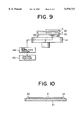
- FIG. 9 is a side elevational view showing a main arm according to yet another embodiment.
- FIG. 10 is a schematic view for explaining an example of a cooling plate in a cooling unit.
- FIG. 1 is a perspective view showing a coating and developing apparatus according to an embodiment of the present invention.
- FIG. 2 is a plan view showing the apparatus shown in FIG. 1.
- the coating and developing apparatus 1 is provided with a cassette station C/S on one side thereof.
- An interface unit I/F for sending and receiving glass substrates G to/from an exposing unit (not shown) is disposed on the other side of the coating and developing apparatus 1.
- An auxiliary arm 4 is disposed on the front side of the cassettes 2 on the cassette station C/S. The auxiliary arm transfers and positions the substrate G that is a treatment substrate, and in addition sends and receives the substrate G to/from the main arm 3 while holding the substrate G.
- auxiliary arm 5 which sends and receives the substrate G to/from the exposing unit (not shown).
- extension portion 6 which sends and receives the substrate G to/from the main arm 3 and a buffer unit 7 where the substrate G temporarily stands by.
- Two main arms 3 are placed in series so as to be movable along the longitudinal direction in the center of the coating and developing apparatus 1.
- a first treatment unit group A and a second treatment unit group B are disposed, respectively.
- a joint portion 8 is located between the first treatment unit group A and the second treatment unit group B, the joint portion temporarily holding and cooling the substrate G.
- a scrubbing unit SCR for scrubbing the substrates G and a developing treatment unit DEV for developing the substrates G are placed side by side on one side of the cassette station C/S.
- two heat processing units HP which are vertically disposed
- a UV treatment unit UV and a cooling unit COL both of which are also vertically disposed, are adjacently located.
- a coating treatment unit COT for performing resist coating treatment and edge removing treatment is disposed.
- an adhesion unit AD for performing hydrophobic treatment for the substrates G and a cooling unit COL, which are vertically disposed
- a heat processing unit HP and a cooling unit COL which are vertically disposed
- two heat processing units HP which are vertically disposed, are adjacently located.
- the main arm 3 is provided with X-axis drive mechanism, Y-axis drive mechanism, Z-axis drive mechanism, and in addition rotating drive mechanism rotating on the Z-axis.
- the main arm 3 appropriately travels along a central passage in the coating and developing apparatus 1 and transfers the substrate G between each of treatment units.
- the main arm 3 transfers the substrate G before being treated into each treatment unit and transfers the substrate G after being treated out from each treatment unit.
- the individual treatment units are integrally disposed so as to reduce the space and improve the efficiency of the treatments.
- FIG. 3 is a perspective view showing a joint portion 8 shown in FIG. 1 and FIG. 2.
- FIG. 4 is a vertical sectional view of FIG. 3.
- a cooling plate 51 which serves as a supporting body to support the substrates G is disposed in the joint portion 8.
- Supporting pins 36 are provided on the four corners of the cooling plate 51.
- the supporting pin 36 vertically moves by means of drive mechanism (not shown).
- the supporting pin 36 receives the substrate G from the main arm 3 when rising and then descends, whereby the substrate G is landed on the cooling plate 51 and the substrate G and the cooling plate 51 are tightly attached. Subsequently the supporting pin 36 rises. In this situation, the supporting pin 36 sends the substrate G to the main arm 3.
- the cooling plate 51 for example, has two-layer structure composed of an upper plate 35a and a lower plate 35b. Pipelines 37a for cooling water to cool the cooling plate 51 and the substrates G are laid in the upper plate 35a. Pipelines 37b for cooling water to cool Peltier elements 38 that are cooling elements are laid in the lower plate 35b.
- More than one Peltier elements 38 are well-orderly disposed in the upper plate 35a in the cooling plate 51.
- the cooling elements and the cooling water pipelines are employed together. Consequently, the substrates are cooled at relatively great speed by means of the cooling water and precisely cooled by means of the cooling elements, resulting in realization of rapid and high-precision cooling.
- Ionizers 39 are placed on the both sides of the cooling plate 51. Ionized gas discharged from the ionizers 39 is blown against the substrates G that are located on the cooling plate 51, which can remove static electricity that is generated when the LCD substrate is tightly attached on the cooling plate 51, thus preventing electrostatic breakdown. Cooled inactive gas such as nitrogen gas is spouted out from the ionizers 39.
- the substrates G which are disposed on the supporting body in the joint portion 8 from the main arm 3, are cooled by means of a gas supplying member or a gas supplying circuit in the ionizers.
- the substrates G in the joint portion 8 are transferred to the cooling unit COL where the substrates are further cooled.
- the substrates G are transferred after being cooled in the joint portion 8 for some time so as to shorten the time required for cooling, resulting in cooling at accurate temperatures.
- FIG. 5 is a perspective view showing the above-described main arm 3.
- FIG. 6 is a side elevational view of FIG. 5.
- 41 in FIG. 5 shows a base which can move horizontally, rise and fall, and revolve. More than one (two in the embodiment) forks 42 which support the substrates G are placed overlapping each other on the base 41.
- a gas supplying member 43 serving as a cooling means is mounted on each of the forks 42.
- a gas supplying system 44 is connected to the gas supplying members 43.
- Gas such as air, nitrogen gas and ionized gas is brought in from the gas supplying system 44, and the gas is supplied to the substrates G through the gas supplying members 43.
- the substrate G touches the fork 42 on each surface while transferring, static electricity may be generated.
- ionized gas is preferably employed for gas.
- a control portion 45 is connected to the gas supplying system 44, the control portion controlling the conditions for blowing gas against substrates, for example, the amount, time or timing of blowing gas. Therefore, it is possible to control and cool the substrate to the desired level by means of substrate cooling by the supplied gas.
- the gas supplying members 43 are individually mounted on each of forks 42 and cool the substrates supported on the forks 42. As shown in FIG. 7, however, the substrates G supported on the forks 42 can be cooled by means of a gas supplying member 43 provided on the base 41 having more than one openings for blowing 43a corresponding to the number of the forks 42. In a way shown in FIG. 6, the cooling level of substrate G on each fork 42 can be individually controlled, while in a way shown in FIG. 7, substrates G on all forks 42 can be uniformly cooled. In the way shown in FIG. 7, hole portions 42a are formed in the forks 42 so as to supply gas to the substrates G through the hole portions 42a. In the way shown in FIG. 7 as well as in FIG. 6, the control portion 45 is connected to the gas supplying system 44 to control the conditions for blowing gas against substrates.
- gas flow through-holes 47 are formed in the forks 42. From the gas flow through-holes 47, gas can be blown against the substrates G for cooling. Also as shown in FIG. 9, a gas flow through-hole 48 can be formed in the base 41 and a gas supplying member 43 connecting therewith is formed on the base 41 in the position just under the forks 42 and gas is supplied to the forks 42.
- the cooling unit COL has a cooling plate 51 as shown in FIG. 10.
- Supporting members 52 composed of members such as resin or rubber are mounted on the cooling plate 51.
- the supporting members 52 support the substrate G.
- cooling plate 51 In the cooling plate 51, more than one cooling elements are disposed or cooling water circulating pipelines are laid.
- the substrate G placed on the cooling plate 51 is cooled by means of the cooling elements or cooling water circulating through the cooling water circulating pipelines.
- the substrate of which surface heat is removed by a transferring member can be precisely cooled.
- a cooling plate having both cooling elements and cooling water circulating pipelines is also available.
- substrates G in cassettes 2 are transferred to a scrubbing unit SCR through an auxiliary arm 4 and a main arm 3 where scrubbing treatment is performed.
- the substrates G are transferred to an adhesion unit AD through a joint portion 8 and the main arm 3 to be given hydrophobic treatment, whereby the fixing characteristic of the resist is improved.
- the substrates G are transferred to a cooling unit COL through the main arm 3 and then transferred to a coating treatment unit COT through the main arm 3 to be coated with resist.
- the substrates G are transferred to a heat processing unit HP through the main arm 3 to be pre-baked. After being transferred to the cooling unit COL through the main arm 3 to be cooled, the substrates G are transferred to an exposing unit through the main arm 3 and an interface portion I/F where the predetermined pattern is exposed.
- Exposed substrates G are transferred again into the apparatus 1 through the interface portion I/F and transferred to the heat processing unit HP through the main arm 3 where post-exposure bake process is performed.
- the substrates G are transferred into the cooling unit COL through the main arm 3, the joint portion 8 and the main arm 3 to be cooled.
- the substrates G are cooled auxiliarily. At this time, the temperature level to lower the temperature of substrate is controlled by adjusting the amount, time, and timing of blowing gas with a control portion 45.
- the substrate G is placed on a cooling plate 51 in the cooling unit COL so as to be cooled as shown in FIG. 10. Since the surface heat of the substrate G is already removed in the joint portion 8 and the main arm 3, the substrate G is cooled on the cooling plate 41 at lower speed than initial cooling, whereby the substrate G can be cooled with high accuracy. In this case, if cooling elements are used as cooling means, substrates can be cooled with higher accuracy. Moreover, the use of cooling plate 51 having cooling elements and cooling water circulating pipelines enables substrates to be cooled rapidly and accurately.
- UV-treated substrates G are put in the predetermined cassettes 2 on the cassette station C/S through the main arm 3 and the auxiliary arm 4.
- the first cooling is conducted in the joint portion 8 and the main arm 3 so as to previously remove surface heat of the substrate G, thus reducing the time of the second cooling.
- the range of the temperature fall caused by the second cooling becomes narrow, thereby facilitating temperature control by means of cooling elements and cooling water circulation and improving accuracy.
- a substrate of which the temperature is raised is cooled to a certain temperature while being transferred, whereby the range of temperatures in cooling in a cooling unit becomes narrow, thus shortening the cooling time. Consequently, the cooling time in substrate cooling can be shortened so that tact time in substrate treatment can be reduced. Practically, the method according to the present invention enables tact time in substrate treatments to be shortened by twenty to thirty percent.
- the present invention is not limited to the above-described embodiment. Instead, various modifications of the present invention are available.
- the present invention is applied to a coating and developing apparatus.
- the present invention is not limited to the coating and developing apparatus, but can be applied to other treatments.
- a LCD substrate is employed for substrate.
- the present invention can be applied to treatments of other substrates such as a semiconductor wafer or the like.
Landscapes
- Engineering & Computer Science (AREA)
- Physics & Mathematics (AREA)
- Microelectronics & Electronic Packaging (AREA)
- General Physics & Mathematics (AREA)
- Manufacturing & Machinery (AREA)
- Computer Hardware Design (AREA)
- Condensed Matter Physics & Semiconductors (AREA)
- Power Engineering (AREA)
- Mechanical Engineering (AREA)
- Thermal Sciences (AREA)
- General Engineering & Computer Science (AREA)
- Container, Conveyance, Adherence, Positioning, Of Wafer (AREA)
- Exposure Of Semiconductors, Excluding Electron Or Ion Beam Exposure (AREA)
- Photosensitive Polymer And Photoresist Processing (AREA)
- Re-Forming, After-Treatment, Cutting And Transporting Of Glass Products (AREA)
Applications Claiming Priority (2)
| Application Number | Priority Date | Filing Date | Title |
|---|---|---|---|
| JP07668597A JP3442253B2 (ja) | 1997-03-13 | 1997-03-13 | 基板処理装置 |
| JP9-076685 | 1997-03-13 |
Publications (1)
| Publication Number | Publication Date |
|---|---|
| US5970717A true US5970717A (en) | 1999-10-26 |
Family
ID=13612312
Family Applications (1)
| Application Number | Title | Priority Date | Filing Date |
|---|---|---|---|
| US09/041,449 Expired - Lifetime US5970717A (en) | 1997-03-13 | 1998-03-12 | Cooling method, cooling apparatus and treatment apparatus |
Country Status (4)
| Country | Link |
|---|---|
| US (1) | US5970717A (zh) |
| JP (1) | JP3442253B2 (zh) |
| KR (1) | KR100352691B1 (zh) |
| TW (1) | TW367539B (zh) |
Cited By (25)
| Publication number | Priority date | Publication date | Assignee | Title |
|---|---|---|---|---|
| US6108937A (en) * | 1998-09-10 | 2000-08-29 | Asm America, Inc. | Method of cooling wafers |
| US6192601B1 (en) * | 1999-02-11 | 2001-02-27 | Applied Materials, Inc. | Method and apparatus for reducing particle contamination during wafer transport |
| US6408537B1 (en) | 1997-07-11 | 2002-06-25 | Asm America, Inc. | Substrate cooling system |
| US6461801B1 (en) | 1999-05-27 | 2002-10-08 | Matrix Integrated Systems, Inc. | Rapid heating and cooling of workpiece chucks |
| US6499777B1 (en) | 1999-05-11 | 2002-12-31 | Matrix Integrated Systems, Inc. | End-effector with integrated cooling mechanism |
| US20030152445A1 (en) * | 2002-02-08 | 2003-08-14 | Takayuki Yamagishi | Semiconductor processing apparatus comprising chamber partitioned into reaction and transfer sections |
| US6609869B2 (en) | 2001-01-04 | 2003-08-26 | Asm America | Transfer chamber with integral loadlock and staging station |
| US20030178467A1 (en) * | 2002-03-20 | 2003-09-25 | Lee Sang Seok | Bonding device for manufacturing liquid crystal display device |
| US6696367B1 (en) | 2002-09-27 | 2004-02-24 | Asm America, Inc. | System for the improved handling of wafers within a process tool |
| US6905333B2 (en) | 2002-09-10 | 2005-06-14 | Axcelis Technologies, Inc. | Method of heating a substrate in a variable temperature process using a fixed temperature chuck |
| US6957690B1 (en) | 1998-09-10 | 2005-10-25 | Asm America, Inc. | Apparatus for thermal treatment of substrates |
| US20060165408A1 (en) * | 2005-01-21 | 2006-07-27 | Tokyo Electron Limited | Coating and developing apparatus and coating and developing method |
| US20070151515A1 (en) * | 2006-01-04 | 2007-07-05 | Kim Jong-Jun | Multi-chamber semiconductor device fabrication apparatus comprising wafer-cooling blade |
| US20070209593A1 (en) * | 2006-03-07 | 2007-09-13 | Ravinder Aggarwal | Semiconductor wafer cooling device |
| US7651306B2 (en) | 2004-12-22 | 2010-01-26 | Applied Materials, Inc. | Cartesian robot cluster tool architecture |
| US7694688B2 (en) | 2007-01-05 | 2010-04-13 | Applied Materials, Inc. | Wet clean system design |
| US7694647B2 (en) | 2004-12-22 | 2010-04-13 | Applied Materials, Inc. | Cluster tool architecture for processing a substrate |
| US7699021B2 (en) | 2004-12-22 | 2010-04-20 | Sokudo Co., Ltd. | Cluster tool substrate throughput optimization |
| US7798764B2 (en) | 2005-12-22 | 2010-09-21 | Applied Materials, Inc. | Substrate processing sequence in a cartesian robot cluster tool |
| US7819079B2 (en) | 2004-12-22 | 2010-10-26 | Applied Materials, Inc. | Cartesian cluster tool configuration for lithography type processes |
| US20100330273A1 (en) * | 2006-07-10 | 2010-12-30 | Dainippon Screen Mfg. Co., Ltd. | Substrate processing apparatus and substrate processing method for heat-treating substrate |
| US7950407B2 (en) | 2007-02-07 | 2011-05-31 | Applied Materials, Inc. | Apparatus for rapid filling of a processing volume |
| CN103223674A (zh) * | 2012-01-26 | 2013-07-31 | 株式会社安川电机 | 搬运机器人 |
| US20130234035A1 (en) * | 2010-07-21 | 2013-09-12 | Tokyo Electron Limited | Ion supply device and workpiece processing system provided with the same |
| US11725272B2 (en) | 2021-11-01 | 2023-08-15 | Canon Kabushiki Kaisha | Method, system and apparatus for cooling a substrate |
Families Citing this family (17)
| Publication number | Priority date | Publication date | Assignee | Title |
|---|---|---|---|---|
| TW439094B (en) * | 1998-02-16 | 2001-06-07 | Komatsu Co Ltd | Apparatus for controlling temperature of substrate |
| JP3260683B2 (ja) * | 1998-02-23 | 2002-02-25 | 鹿児島日本電気株式会社 | 基板移載装置 |
| JP3684325B2 (ja) * | 1999-07-19 | 2005-08-17 | 東京エレクトロン株式会社 | 基板処理装置 |
| TW511169B (en) * | 2000-02-01 | 2002-11-21 | Tokyo Electron Ltd | Substrate processing apparatus and substrate processing method |
| JP3910791B2 (ja) * | 2000-09-19 | 2007-04-25 | 東京エレクトロン株式会社 | 基板の熱処理方法及び基板の熱処理装置 |
| JP2007073564A (ja) * | 2005-09-02 | 2007-03-22 | Fujitsu Ltd | アッシング装置 |
| JP4833005B2 (ja) * | 2006-09-11 | 2011-12-07 | 大日本スクリーン製造株式会社 | 基板処理装置および基板処理方法 |
| KR100955490B1 (ko) * | 2008-05-21 | 2010-04-30 | 세메스 주식회사 | 평판 디스플레이 제조에 사용되는 베이크 장치 및 방법 |
| JP5635378B2 (ja) * | 2010-11-30 | 2014-12-03 | 日東電工株式会社 | 半導体ウエハ搬送方法および半導体ウエハ搬送装置 |
| JP2013074112A (ja) * | 2011-09-28 | 2013-04-22 | Yaskawa Electric Corp | ハンドおよび基板搬送装置 |
| JP5959216B2 (ja) * | 2012-02-06 | 2016-08-02 | 日東電工株式会社 | 基板搬送方法および基板搬送装置 |
| JP2013168417A (ja) * | 2012-02-14 | 2013-08-29 | Nitto Denko Corp | 基板搬送方法および基板搬送装置 |
| JP5963242B2 (ja) * | 2012-03-07 | 2016-08-03 | 日本特殊陶業株式会社 | 搬送装置およびセラミック部材 |
| JP6808395B2 (ja) * | 2016-08-18 | 2021-01-06 | 株式会社Screenホールディングス | 基板処理装置 |
| TWI687291B (zh) * | 2018-10-08 | 2020-03-11 | 聚昌科技股份有限公司 | 三重托叉式之機械手臂結構及其角度監測模組 |
| CN111061132A (zh) * | 2018-10-17 | 2020-04-24 | 聚昌科技股份有限公司 | 三重托叉式的机械手臂结构及其角度监测模块 |
| KR102583261B1 (ko) * | 2020-10-28 | 2023-09-27 | 세메스 주식회사 | 기판 처리 장치 및 기판 처리 방법 |
Citations (6)
| Publication number | Priority date | Publication date | Assignee | Title |
|---|---|---|---|---|
| US4414758A (en) * | 1981-03-23 | 1983-11-15 | Fritz Peter | Conveyor for cooling and removal of objects from an in-line sectional production machine |
| US4667478A (en) * | 1984-09-18 | 1987-05-26 | Durotech Corporation | Apparatus and method for the cryogenic treatment and heating of materials |
| US4777733A (en) * | 1987-01-09 | 1988-10-18 | Iwatani & Co. Ltd. | Method of manufacturing shoes |
| US4934151A (en) * | 1989-07-07 | 1990-06-19 | Kyokujitsu Company., Ltd. | Continuous multistage thermal processing apparatus, freezing control method for use by the apparatus, and apparatus for preparing a recording medium for the control method |
| US5315834A (en) * | 1992-08-14 | 1994-05-31 | Feliks Garunts | Room air environment conditioner |
| US5551165A (en) * | 1995-04-13 | 1996-09-03 | Texas Instruments Incorporated | Enhanced cleansing process for wafer handling implements |
Family Cites Families (1)
| Publication number | Priority date | Publication date | Assignee | Title |
|---|---|---|---|---|
| JPS6378546A (ja) * | 1986-09-22 | 1988-04-08 | Hitachi Ltd | ウエハハンドリング装置 |
-
1997
- 1997-03-13 JP JP07668597A patent/JP3442253B2/ja not_active Expired - Fee Related
-
1998
- 1998-02-17 TW TW087102180A patent/TW367539B/zh not_active IP Right Cessation
- 1998-03-12 US US09/041,449 patent/US5970717A/en not_active Expired - Lifetime
- 1998-03-12 KR KR10-1998-0008320A patent/KR100352691B1/ko not_active IP Right Cessation
Patent Citations (6)
| Publication number | Priority date | Publication date | Assignee | Title |
|---|---|---|---|---|
| US4414758A (en) * | 1981-03-23 | 1983-11-15 | Fritz Peter | Conveyor for cooling and removal of objects from an in-line sectional production machine |
| US4667478A (en) * | 1984-09-18 | 1987-05-26 | Durotech Corporation | Apparatus and method for the cryogenic treatment and heating of materials |
| US4777733A (en) * | 1987-01-09 | 1988-10-18 | Iwatani & Co. Ltd. | Method of manufacturing shoes |
| US4934151A (en) * | 1989-07-07 | 1990-06-19 | Kyokujitsu Company., Ltd. | Continuous multistage thermal processing apparatus, freezing control method for use by the apparatus, and apparatus for preparing a recording medium for the control method |
| US5315834A (en) * | 1992-08-14 | 1994-05-31 | Feliks Garunts | Room air environment conditioner |
| US5551165A (en) * | 1995-04-13 | 1996-09-03 | Texas Instruments Incorporated | Enhanced cleansing process for wafer handling implements |
Cited By (43)
| Publication number | Priority date | Publication date | Assignee | Title |
|---|---|---|---|---|
| US6408537B1 (en) | 1997-07-11 | 2002-06-25 | Asm America, Inc. | Substrate cooling system |
| US6578287B2 (en) | 1997-07-11 | 2003-06-17 | Asm America, Inc. | Substrate cooling system and method |
| US6108937A (en) * | 1998-09-10 | 2000-08-29 | Asm America, Inc. | Method of cooling wafers |
| US6209220B1 (en) * | 1998-09-10 | 2001-04-03 | Asm America, Inc. | Apparatus for cooling substrates |
| US6957690B1 (en) | 1998-09-10 | 2005-10-25 | Asm America, Inc. | Apparatus for thermal treatment of substrates |
| US20050229855A1 (en) * | 1998-09-10 | 2005-10-20 | Ivo Raaijmakers | Apparatus for thermal treatment of substrates |
| US6192601B1 (en) * | 1999-02-11 | 2001-02-27 | Applied Materials, Inc. | Method and apparatus for reducing particle contamination during wafer transport |
| US6499777B1 (en) | 1999-05-11 | 2002-12-31 | Matrix Integrated Systems, Inc. | End-effector with integrated cooling mechanism |
| US6461801B1 (en) | 1999-05-27 | 2002-10-08 | Matrix Integrated Systems, Inc. | Rapid heating and cooling of workpiece chucks |
| US6609869B2 (en) | 2001-01-04 | 2003-08-26 | Asm America | Transfer chamber with integral loadlock and staging station |
| US6899507B2 (en) | 2002-02-08 | 2005-05-31 | Asm Japan K.K. | Semiconductor processing apparatus comprising chamber partitioned into reaction and transfer sections |
| US20050118001A1 (en) * | 2002-02-08 | 2005-06-02 | Takayuki Yamagishi | Semiconductor processing apparatus comprising chamber partitioned into reaction and transfer sections |
| US7021881B2 (en) | 2002-02-08 | 2006-04-04 | Asm Japan K.K. | Semiconductor processing apparatus comprising chamber partitioned into reaction and transfer sections |
| US20030152445A1 (en) * | 2002-02-08 | 2003-08-14 | Takayuki Yamagishi | Semiconductor processing apparatus comprising chamber partitioned into reaction and transfer sections |
| US20030178467A1 (en) * | 2002-03-20 | 2003-09-25 | Lee Sang Seok | Bonding device for manufacturing liquid crystal display device |
| US7341641B2 (en) * | 2002-03-20 | 2008-03-11 | Lg.Philips Lcd Co., Ltd. | Bonding device for manufacturing liquid crystal display device |
| US6905333B2 (en) | 2002-09-10 | 2005-06-14 | Axcelis Technologies, Inc. | Method of heating a substrate in a variable temperature process using a fixed temperature chuck |
| US7485190B2 (en) | 2002-09-10 | 2009-02-03 | Axcelis Technologies, Inc. | Apparatus for heating a substrate in a variable temperature process using a fixed temperature chuck |
| US20050166845A1 (en) * | 2002-09-10 | 2005-08-04 | Gerald Cox | Method of heating a substrate in a variable temperature process using a fixed temperature chuck |
| US20040062627A1 (en) * | 2002-09-27 | 2004-04-01 | Ravinder Aggarwal | System for the improved handling of wafers within a process tool |
| US6696367B1 (en) | 2002-09-27 | 2004-02-24 | Asm America, Inc. | System for the improved handling of wafers within a process tool |
| US8911193B2 (en) | 2004-12-22 | 2014-12-16 | Applied Materials, Inc. | Substrate processing sequence in a cartesian robot cluster tool |
| US8550031B2 (en) | 2004-12-22 | 2013-10-08 | Applied Materials, Inc. | Cluster tool architecture for processing a substrate |
| US7651306B2 (en) | 2004-12-22 | 2010-01-26 | Applied Materials, Inc. | Cartesian robot cluster tool architecture |
| US7925377B2 (en) | 2004-12-22 | 2011-04-12 | Applied Materials, Inc. | Cluster tool architecture for processing a substrate |
| US7694647B2 (en) | 2004-12-22 | 2010-04-13 | Applied Materials, Inc. | Cluster tool architecture for processing a substrate |
| US7699021B2 (en) | 2004-12-22 | 2010-04-20 | Sokudo Co., Ltd. | Cluster tool substrate throughput optimization |
| US7743728B2 (en) | 2004-12-22 | 2010-06-29 | Applied Materials, Inc. | Cluster tool architecture for processing a substrate |
| US7819079B2 (en) | 2004-12-22 | 2010-10-26 | Applied Materials, Inc. | Cartesian cluster tool configuration for lithography type processes |
| US7322756B2 (en) | 2005-01-21 | 2008-01-29 | Tokyo Electron Limited | Coating and developing apparatus and coating and developing method |
| US20060165408A1 (en) * | 2005-01-21 | 2006-07-27 | Tokyo Electron Limited | Coating and developing apparatus and coating and developing method |
| US7798764B2 (en) | 2005-12-22 | 2010-09-21 | Applied Materials, Inc. | Substrate processing sequence in a cartesian robot cluster tool |
| US8066466B2 (en) | 2005-12-22 | 2011-11-29 | Applied Materials, Inc. | Substrate processing sequence in a Cartesian robot cluster tool |
| US20070151515A1 (en) * | 2006-01-04 | 2007-07-05 | Kim Jong-Jun | Multi-chamber semiconductor device fabrication apparatus comprising wafer-cooling blade |
| US20070209593A1 (en) * | 2006-03-07 | 2007-09-13 | Ravinder Aggarwal | Semiconductor wafer cooling device |
| US20100330273A1 (en) * | 2006-07-10 | 2010-12-30 | Dainippon Screen Mfg. Co., Ltd. | Substrate processing apparatus and substrate processing method for heat-treating substrate |
| US7694688B2 (en) | 2007-01-05 | 2010-04-13 | Applied Materials, Inc. | Wet clean system design |
| US7950407B2 (en) | 2007-02-07 | 2011-05-31 | Applied Materials, Inc. | Apparatus for rapid filling of a processing volume |
| US20130234035A1 (en) * | 2010-07-21 | 2013-09-12 | Tokyo Electron Limited | Ion supply device and workpiece processing system provided with the same |
| US8692208B2 (en) * | 2010-07-21 | 2014-04-08 | Tokyo Electron Limted | Ion supply device and workpiece processing system provided with the same |
| CN103223674A (zh) * | 2012-01-26 | 2013-07-31 | 株式会社安川电机 | 搬运机器人 |
| CN103223674B (zh) * | 2012-01-26 | 2016-06-08 | 株式会社安川电机 | 搬运机器人 |
| US11725272B2 (en) | 2021-11-01 | 2023-08-15 | Canon Kabushiki Kaisha | Method, system and apparatus for cooling a substrate |
Also Published As
| Publication number | Publication date |
|---|---|
| JPH10256344A (ja) | 1998-09-25 |
| JP3442253B2 (ja) | 2003-09-02 |
| KR19980080192A (ko) | 1998-11-25 |
| KR100352691B1 (ko) | 2003-04-07 |
| TW367539B (en) | 1999-08-21 |
Similar Documents
| Publication | Publication Date | Title |
|---|---|---|
| US5970717A (en) | Cooling method, cooling apparatus and treatment apparatus | |
| US6227786B1 (en) | Substrate treating apparatus | |
| KR100352690B1 (ko) | 냉각장치,냉각방법및처리장치 | |
| JP3202929B2 (ja) | 処理システム | |
| US6464789B1 (en) | Substrate processing apparatus | |
| KR100574303B1 (ko) | 기판처리장치 | |
| KR20010054426A (ko) | 포토리소그라피 공정을 위한 반도체 제조장치 | |
| JP2000012447A (ja) | 熱処理装置及び熱処理方法 | |
| KR100697939B1 (ko) | 도포현상처리방법 및 도포현상처리시스템 | |
| KR100480668B1 (ko) | 기판처리장치 및 기판처리방법 | |
| KR100439608B1 (ko) | 레지스트도포·현상처리시스템 | |
| US6436609B1 (en) | Photolithographic apparatus composed of coater/developer and a plurality of steppers in parallel connected thereto | |
| KR100704749B1 (ko) | 기판처리장치 및 기판처리방법 | |
| JP2000124127A (ja) | レジスト塗布・現像装置、ならびにそれに用いる基板加熱処理装置および基板搬送装置 | |
| KR100292322B1 (ko) | 기판처리장치및기판반송방법 | |
| US6008978A (en) | Discharging method and processing apparatus having discharging function | |
| KR100793171B1 (ko) | 베이크 공정 장치 및 상기 베이크 공정 장치에 구비되는 가열판의 냉각 방법 | |
| JPH10275766A (ja) | 基板処理装置 | |
| KR101069821B1 (ko) | 반도체 기판 제조에 사용되는 포토 리소그래피 장치 | |
| KR20010054262A (ko) | 포토리소그라피 공정을 위한 반도체 제조장치 | |
| JP4104909B2 (ja) | 基板冷却装置および処理装置 | |
| KR101842121B1 (ko) | 기판 처리 장치 및 이의 구동 속도 제어 방법 | |
| US20020088544A1 (en) | Substrate processing apparatus | |
| KR100432880B1 (ko) | 반도체 제조 공정에서 사용되는 스피너 시스템 | |
| KR102000016B1 (ko) | 기판 처리 장치, 기판 지지 유닛 및 그 제작방법 |
Legal Events
| Date | Code | Title | Description |
|---|---|---|---|
| AS | Assignment |
Owner name: NOKIA MOBILE PHONES LIMITED, FINLAND Free format text: ;ASSIGNOR:KOLINEN, PETTERI;REEL/FRAME:008948/0186 Effective date: 19980122 |
|
| AS | Assignment |
Owner name: TOKYO ELECTRON LIMITED, JAPAN Free format text: ASSIGNMENT OF ASSIGNORS INTEREST;ASSIGNOR:TATEYAMA, KIYOSHA;REEL/FRAME:009039/0780 Effective date: 19980126 |
|
| STCF | Information on status: patent grant |
Free format text: PATENTED CASE |
|
| FEPP | Fee payment procedure |
Free format text: PAYOR NUMBER ASSIGNED (ORIGINAL EVENT CODE: ASPN); ENTITY STATUS OF PATENT OWNER: LARGE ENTITY |
|
| FPAY | Fee payment |
Year of fee payment: 4 |
|
| FPAY | Fee payment |
Year of fee payment: 8 |
|
| FPAY | Fee payment |
Year of fee payment: 12 |