US5484686A - Optical recording media and information recording and reproducing units - Google Patents
Optical recording media and information recording and reproducing units Download PDFInfo
- Publication number
- US5484686A US5484686A US08/205,768 US20576894A US5484686A US 5484686 A US5484686 A US 5484686A US 20576894 A US20576894 A US 20576894A US 5484686 A US5484686 A US 5484686A
- Authority
- US
- United States
- Prior art keywords
- film
- recording
- thickness
- recording film
- absorptivity
- Prior art date
- Legal status (The legal status is an assumption and is not a legal conclusion. Google has not performed a legal analysis and makes no representation as to the accuracy of the status listed.)
- Ceased
Links
Images


Classifications
-
- G—PHYSICS
- G11—INFORMATION STORAGE
- G11B—INFORMATION STORAGE BASED ON RELATIVE MOVEMENT BETWEEN RECORD CARRIER AND TRANSDUCER
- G11B7/00—Recording or reproducing by optical means, e.g. recording using a thermal beam of optical radiation by modifying optical properties or the physical structure, reproducing using an optical beam at lower power by sensing optical properties; Record carriers therefor
- G11B7/24—Record carriers characterised by shape, structure or physical properties, or by the selection of the material
- G11B7/241—Record carriers characterised by shape, structure or physical properties, or by the selection of the material characterised by the selection of the material
- G11B7/252—Record carriers characterised by shape, structure or physical properties, or by the selection of the material characterised by the selection of the material of layers other than recording layers
- G11B7/257—Record carriers characterised by shape, structure or physical properties, or by the selection of the material characterised by the selection of the material of layers other than recording layers of layers having properties involved in recording or reproduction, e.g. optical interference layers or sensitising layers or dielectric layers, which are protecting the recording layers
-
- G—PHYSICS
- G11—INFORMATION STORAGE
- G11B—INFORMATION STORAGE BASED ON RELATIVE MOVEMENT BETWEEN RECORD CARRIER AND TRANSDUCER
- G11B7/00—Recording or reproducing by optical means, e.g. recording using a thermal beam of optical radiation by modifying optical properties or the physical structure, reproducing using an optical beam at lower power by sensing optical properties; Record carriers therefor
- G11B7/24—Record carriers characterised by shape, structure or physical properties, or by the selection of the material
- G11B7/241—Record carriers characterised by shape, structure or physical properties, or by the selection of the material characterised by the selection of the material
- G11B7/242—Record carriers characterised by shape, structure or physical properties, or by the selection of the material characterised by the selection of the material of recording layers
-
- G—PHYSICS
- G11—INFORMATION STORAGE
- G11B—INFORMATION STORAGE BASED ON RELATIVE MOVEMENT BETWEEN RECORD CARRIER AND TRANSDUCER
- G11B7/00—Recording or reproducing by optical means, e.g. recording using a thermal beam of optical radiation by modifying optical properties or the physical structure, reproducing using an optical beam at lower power by sensing optical properties; Record carriers therefor
- G11B7/004—Recording, reproducing or erasing methods; Read, write or erase circuits therefor
- G11B7/0045—Recording
-
- G—PHYSICS
- G11—INFORMATION STORAGE
- G11B—INFORMATION STORAGE BASED ON RELATIVE MOVEMENT BETWEEN RECORD CARRIER AND TRANSDUCER
- G11B7/00—Recording or reproducing by optical means, e.g. recording using a thermal beam of optical radiation by modifying optical properties or the physical structure, reproducing using an optical beam at lower power by sensing optical properties; Record carriers therefor
- G11B7/004—Recording, reproducing or erasing methods; Read, write or erase circuits therefor
- G11B7/0055—Erasing
- G11B7/00557—Erasing involving phase-change media
-
- G—PHYSICS
- G11—INFORMATION STORAGE
- G11B—INFORMATION STORAGE BASED ON RELATIVE MOVEMENT BETWEEN RECORD CARRIER AND TRANSDUCER
- G11B7/00—Recording or reproducing by optical means, e.g. recording using a thermal beam of optical radiation by modifying optical properties or the physical structure, reproducing using an optical beam at lower power by sensing optical properties; Record carriers therefor
- G11B7/24—Record carriers characterised by shape, structure or physical properties, or by the selection of the material
- G11B7/241—Record carriers characterised by shape, structure or physical properties, or by the selection of the material characterised by the selection of the material
- G11B7/242—Record carriers characterised by shape, structure or physical properties, or by the selection of the material characterised by the selection of the material of recording layers
- G11B7/243—Record carriers characterised by shape, structure or physical properties, or by the selection of the material characterised by the selection of the material of recording layers comprising inorganic materials only, e.g. ablative layers
-
- G—PHYSICS
- G11—INFORMATION STORAGE
- G11B—INFORMATION STORAGE BASED ON RELATIVE MOVEMENT BETWEEN RECORD CARRIER AND TRANSDUCER
- G11B7/00—Recording or reproducing by optical means, e.g. recording using a thermal beam of optical radiation by modifying optical properties or the physical structure, reproducing using an optical beam at lower power by sensing optical properties; Record carriers therefor
- G11B7/24—Record carriers characterised by shape, structure or physical properties, or by the selection of the material
- G11B7/241—Record carriers characterised by shape, structure or physical properties, or by the selection of the material characterised by the selection of the material
- G11B7/252—Record carriers characterised by shape, structure or physical properties, or by the selection of the material characterised by the selection of the material of layers other than recording layers
- G11B7/258—Record carriers characterised by shape, structure or physical properties, or by the selection of the material characterised by the selection of the material of layers other than recording layers of reflective layers
-
- G—PHYSICS
- G11—INFORMATION STORAGE
- G11B—INFORMATION STORAGE BASED ON RELATIVE MOVEMENT BETWEEN RECORD CARRIER AND TRANSDUCER
- G11B7/00—Recording or reproducing by optical means, e.g. recording using a thermal beam of optical radiation by modifying optical properties or the physical structure, reproducing using an optical beam at lower power by sensing optical properties; Record carriers therefor
- G11B7/24—Record carriers characterised by shape, structure or physical properties, or by the selection of the material
- G11B7/241—Record carriers characterised by shape, structure or physical properties, or by the selection of the material characterised by the selection of the material
- G11B7/242—Record carriers characterised by shape, structure or physical properties, or by the selection of the material characterised by the selection of the material of recording layers
- G11B7/243—Record carriers characterised by shape, structure or physical properties, or by the selection of the material characterised by the selection of the material of recording layers comprising inorganic materials only, e.g. ablative layers
- G11B2007/24302—Metals or metalloids
- G11B2007/24304—Metals or metalloids group 2 or 12 elements (e.g. Be, Ca, Mg, Zn, Cd)
-
- G—PHYSICS
- G11—INFORMATION STORAGE
- G11B—INFORMATION STORAGE BASED ON RELATIVE MOVEMENT BETWEEN RECORD CARRIER AND TRANSDUCER
- G11B7/00—Recording or reproducing by optical means, e.g. recording using a thermal beam of optical radiation by modifying optical properties or the physical structure, reproducing using an optical beam at lower power by sensing optical properties; Record carriers therefor
- G11B7/24—Record carriers characterised by shape, structure or physical properties, or by the selection of the material
- G11B7/241—Record carriers characterised by shape, structure or physical properties, or by the selection of the material characterised by the selection of the material
- G11B7/242—Record carriers characterised by shape, structure or physical properties, or by the selection of the material characterised by the selection of the material of recording layers
- G11B7/243—Record carriers characterised by shape, structure or physical properties, or by the selection of the material characterised by the selection of the material of recording layers comprising inorganic materials only, e.g. ablative layers
- G11B2007/24302—Metals or metalloids
- G11B2007/24308—Metals or metalloids transition metal elements of group 11 (Cu, Ag, Au)
-
- G—PHYSICS
- G11—INFORMATION STORAGE
- G11B—INFORMATION STORAGE BASED ON RELATIVE MOVEMENT BETWEEN RECORD CARRIER AND TRANSDUCER
- G11B7/00—Recording or reproducing by optical means, e.g. recording using a thermal beam of optical radiation by modifying optical properties or the physical structure, reproducing using an optical beam at lower power by sensing optical properties; Record carriers therefor
- G11B7/24—Record carriers characterised by shape, structure or physical properties, or by the selection of the material
- G11B7/241—Record carriers characterised by shape, structure or physical properties, or by the selection of the material characterised by the selection of the material
- G11B7/242—Record carriers characterised by shape, structure or physical properties, or by the selection of the material characterised by the selection of the material of recording layers
- G11B7/243—Record carriers characterised by shape, structure or physical properties, or by the selection of the material characterised by the selection of the material of recording layers comprising inorganic materials only, e.g. ablative layers
- G11B2007/24302—Metals or metalloids
- G11B2007/2431—Metals or metalloids group 13 elements (B, Al, Ga, In)
-
- G—PHYSICS
- G11—INFORMATION STORAGE
- G11B—INFORMATION STORAGE BASED ON RELATIVE MOVEMENT BETWEEN RECORD CARRIER AND TRANSDUCER
- G11B7/00—Recording or reproducing by optical means, e.g. recording using a thermal beam of optical radiation by modifying optical properties or the physical structure, reproducing using an optical beam at lower power by sensing optical properties; Record carriers therefor
- G11B7/24—Record carriers characterised by shape, structure or physical properties, or by the selection of the material
- G11B7/241—Record carriers characterised by shape, structure or physical properties, or by the selection of the material characterised by the selection of the material
- G11B7/242—Record carriers characterised by shape, structure or physical properties, or by the selection of the material characterised by the selection of the material of recording layers
- G11B7/243—Record carriers characterised by shape, structure or physical properties, or by the selection of the material characterised by the selection of the material of recording layers comprising inorganic materials only, e.g. ablative layers
- G11B2007/24302—Metals or metalloids
- G11B2007/24312—Metals or metalloids group 14 elements (e.g. Si, Ge, Sn)
-
- G—PHYSICS
- G11—INFORMATION STORAGE
- G11B—INFORMATION STORAGE BASED ON RELATIVE MOVEMENT BETWEEN RECORD CARRIER AND TRANSDUCER
- G11B7/00—Recording or reproducing by optical means, e.g. recording using a thermal beam of optical radiation by modifying optical properties or the physical structure, reproducing using an optical beam at lower power by sensing optical properties; Record carriers therefor
- G11B7/24—Record carriers characterised by shape, structure or physical properties, or by the selection of the material
- G11B7/241—Record carriers characterised by shape, structure or physical properties, or by the selection of the material characterised by the selection of the material
- G11B7/242—Record carriers characterised by shape, structure or physical properties, or by the selection of the material characterised by the selection of the material of recording layers
- G11B7/243—Record carriers characterised by shape, structure or physical properties, or by the selection of the material characterised by the selection of the material of recording layers comprising inorganic materials only, e.g. ablative layers
- G11B2007/24302—Metals or metalloids
- G11B2007/24314—Metals or metalloids group 15 elements (e.g. Sb, Bi)
-
- G—PHYSICS
- G11—INFORMATION STORAGE
- G11B—INFORMATION STORAGE BASED ON RELATIVE MOVEMENT BETWEEN RECORD CARRIER AND TRANSDUCER
- G11B7/00—Recording or reproducing by optical means, e.g. recording using a thermal beam of optical radiation by modifying optical properties or the physical structure, reproducing using an optical beam at lower power by sensing optical properties; Record carriers therefor
- G11B7/24—Record carriers characterised by shape, structure or physical properties, or by the selection of the material
- G11B7/241—Record carriers characterised by shape, structure or physical properties, or by the selection of the material characterised by the selection of the material
- G11B7/242—Record carriers characterised by shape, structure or physical properties, or by the selection of the material characterised by the selection of the material of recording layers
- G11B7/243—Record carriers characterised by shape, structure or physical properties, or by the selection of the material characterised by the selection of the material of recording layers comprising inorganic materials only, e.g. ablative layers
- G11B2007/24302—Metals or metalloids
- G11B2007/24316—Metals or metalloids group 16 elements (i.e. chalcogenides, Se, Te)
-
- G—PHYSICS
- G11—INFORMATION STORAGE
- G11B—INFORMATION STORAGE BASED ON RELATIVE MOVEMENT BETWEEN RECORD CARRIER AND TRANSDUCER
- G11B7/00—Recording or reproducing by optical means, e.g. recording using a thermal beam of optical radiation by modifying optical properties or the physical structure, reproducing using an optical beam at lower power by sensing optical properties; Record carriers therefor
- G11B7/004—Recording, reproducing or erasing methods; Read, write or erase circuits therefor
- G11B7/0045—Recording
- G11B7/00454—Recording involving phase-change effects
-
- G—PHYSICS
- G11—INFORMATION STORAGE
- G11B—INFORMATION STORAGE BASED ON RELATIVE MOVEMENT BETWEEN RECORD CARRIER AND TRANSDUCER
- G11B7/00—Recording or reproducing by optical means, e.g. recording using a thermal beam of optical radiation by modifying optical properties or the physical structure, reproducing using an optical beam at lower power by sensing optical properties; Record carriers therefor
- G11B7/004—Recording, reproducing or erasing methods; Read, write or erase circuits therefor
- G11B7/005—Reproducing
- G11B7/0052—Reproducing involving reflectivity, absorption or colour changes
-
- G—PHYSICS
- G11—INFORMATION STORAGE
- G11B—INFORMATION STORAGE BASED ON RELATIVE MOVEMENT BETWEEN RECORD CARRIER AND TRANSDUCER
- G11B7/00—Recording or reproducing by optical means, e.g. recording using a thermal beam of optical radiation by modifying optical properties or the physical structure, reproducing using an optical beam at lower power by sensing optical properties; Record carriers therefor
- G11B7/24—Record carriers characterised by shape, structure or physical properties, or by the selection of the material
- G11B7/241—Record carriers characterised by shape, structure or physical properties, or by the selection of the material characterised by the selection of the material
- G11B7/252—Record carriers characterised by shape, structure or physical properties, or by the selection of the material characterised by the selection of the material of layers other than recording layers
- G11B7/253—Record carriers characterised by shape, structure or physical properties, or by the selection of the material characterised by the selection of the material of layers other than recording layers of substrates
- G11B7/2531—Record carriers characterised by shape, structure or physical properties, or by the selection of the material characterised by the selection of the material of layers other than recording layers of substrates comprising glass
-
- G—PHYSICS
- G11—INFORMATION STORAGE
- G11B—INFORMATION STORAGE BASED ON RELATIVE MOVEMENT BETWEEN RECORD CARRIER AND TRANSDUCER
- G11B7/00—Recording or reproducing by optical means, e.g. recording using a thermal beam of optical radiation by modifying optical properties or the physical structure, reproducing using an optical beam at lower power by sensing optical properties; Record carriers therefor
- G11B7/24—Record carriers characterised by shape, structure or physical properties, or by the selection of the material
- G11B7/241—Record carriers characterised by shape, structure or physical properties, or by the selection of the material characterised by the selection of the material
- G11B7/252—Record carriers characterised by shape, structure or physical properties, or by the selection of the material characterised by the selection of the material of layers other than recording layers
- G11B7/258—Record carriers characterised by shape, structure or physical properties, or by the selection of the material characterised by the selection of the material of layers other than recording layers of reflective layers
- G11B7/2585—Record carriers characterised by shape, structure or physical properties, or by the selection of the material characterised by the selection of the material of layers other than recording layers of reflective layers based on aluminium
-
- G—PHYSICS
- G11—INFORMATION STORAGE
- G11B—INFORMATION STORAGE BASED ON RELATIVE MOVEMENT BETWEEN RECORD CARRIER AND TRANSDUCER
- G11B7/00—Recording or reproducing by optical means, e.g. recording using a thermal beam of optical radiation by modifying optical properties or the physical structure, reproducing using an optical beam at lower power by sensing optical properties; Record carriers therefor
- G11B7/24—Record carriers characterised by shape, structure or physical properties, or by the selection of the material
- G11B7/241—Record carriers characterised by shape, structure or physical properties, or by the selection of the material characterised by the selection of the material
- G11B7/252—Record carriers characterised by shape, structure or physical properties, or by the selection of the material characterised by the selection of the material of layers other than recording layers
- G11B7/258—Record carriers characterised by shape, structure or physical properties, or by the selection of the material characterised by the selection of the material of layers other than recording layers of reflective layers
- G11B7/2595—Record carriers characterised by shape, structure or physical properties, or by the selection of the material characterised by the selection of the material of layers other than recording layers of reflective layers based on gold
-
- Y—GENERAL TAGGING OF NEW TECHNOLOGICAL DEVELOPMENTS; GENERAL TAGGING OF CROSS-SECTIONAL TECHNOLOGIES SPANNING OVER SEVERAL SECTIONS OF THE IPC; TECHNICAL SUBJECTS COVERED BY FORMER USPC CROSS-REFERENCE ART COLLECTIONS [XRACs] AND DIGESTS
- Y10—TECHNICAL SUBJECTS COVERED BY FORMER USPC
- Y10S—TECHNICAL SUBJECTS COVERED BY FORMER USPC CROSS-REFERENCE ART COLLECTIONS [XRACs] AND DIGESTS
- Y10S430/00—Radiation imagery chemistry: process, composition, or product thereof
- Y10S430/146—Laser beam
Definitions
- This invention relates to rewritable optical recording media in which information can be recorded, reproduced and erased by using light and heat, a method of information recording, reproducing and erasing in said optical recording media and units therefor.
- optical information recording and reproducing units information is recorded or erased by means of a change of optical characteristic (energy reflectivity: to be referred to as "reflectivity” hereinbelow) according to the phase-change between the amorphous phase and the crystalline phase caused when a laser power is changed for irradiation.
- Various methods for optical information recording and reproducing have hitherto been proposed. As shown in the following known examples, the reflectivities of conventional optical disks are smaller in the amorphous state corresponding to record than in the crystalline state corresponding to erasion.
- Known examples Chemistry and Industry, Vol. 39, No. 3, 1986, P. 174; a disk using a Te 87 Ge 8 Sn 5 recording material, described in Applied Physics Letters, Vol.
- FUJITSU. 38, 2, 1987, page 144 describes a disk using an SeInSb recording material as a disk having a higher reflectivity in the recording state than in the erasing state.
- This disk utilizes crystal I and crystal II, which have different crystalline structures.
- the erasing is effected by a method of recrystallizing the recorded bit by heating it to a temperature at which the recorded bit is not melted (to be referred to as "solid phase transformation” hereinbelow).
- solid phase transformation a temperature at which the recorded bit is not melted
- the number of incompletely erased parts is large.
- SbSeTeGe recording material described in Extended Abstracts (The 35th Spring Meeting 1985); the Japan Society of Applied physics and Related Societies 28P-ZQ-12, 1988, page 842
- the overwrite method is classified into two erasing ways. One is that the erasing is carried out by crystallizing an amorphous part in the solid phase state.
- the erasability is -25 dB, and incompletely erased parts still remain (solid phase transformation).
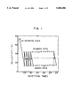
- the erasability is -15 dB as shown in FIG. 2, and the number of incompletely erased parts is larger in this way than in the solid phase transformation.
- Sb 2 (Te-Se) 3 -GeTe described in Technical Report of Electronic Information Communication Society, Shingaku Giho, Vol. 87, No. 310, CPM87-90, 1987, page 41, the erasing method uses the solid phase transformation.
- the erasability with a laser power of 10 mW is about 30 dB as shown in FIG. 3.
- the laser power is 15 mW or more, the liquid phase transformation takes place, and the erasability becomes high. It is pointed out, however, that the high erasability is because unrecorded parts (crystal parts) are melted by irradiation with a laser power of 15 mW or more melts to become amorphous but it is not because recorded bits are erased.
- the errasing method comprises increasing the laser power once [to not less than Tm (melting point)] to melt a recorded spot, and then, in the course of cooling, irradiating an elliptic laser spot beam in a power of not less than Tx (crystallization temperature) and not more than Tm, and this method gives an erasability of -40 dB.
- the problem is that the non-erased part remains in the cases of both the solid phase transformation and the liquid phase transformation, and any high erasability cannot be achieved.
- the double beam method gives a high erasability, but requires a complicated unit therefor, which requirement is a problem.
- the optical properties (refractive index n, extinction coefficient k) of known recording films are as follows (see TABLE 1).
- the refractive indices and extinction coefficients of the known examples are all in the relationships of n amo ⁇ n cry and k amo ⁇ k cry, and in particular, the refractive indices in the amorphous state are characteristically smaller than those in the crystalline state.
- the above object is to carry out the incomplete erasion-reduced erasion by acquiring larger reflectivity in the recorded state of an optical recording medium or in an amorphous state of a recording film constituting the optical recording medium than in the erased state of the optical recording medium or in a crystalline state of the recording film constituting the optical recording medium, or by acquiring a smaller energy absorptivity (to be referred to as "absorptivity" hereinbelow) in the recorded state of the optical recording medium or in an amorphous state of the recording film constituting the optical recording medium than in the erased state of the optical recording medium or in a crystalline state of the recording film constituting the optical recording medium, and by melting both the amorphous recorded part of the recording film and the inevitably copresent unrecorded part (crystal).
- the term "recorded state” used in this invention refers to a complete amorphous state, but also may indicate a state in which the crystalline phase is copresent with the amorphous phase [the amount of the amorphous phase in the recording film is 50 vol. % or more].
- the amorphous phase can be defined as the structure having random network chemical bonding of Te and the other elements, and also defined as non diffraction peaks using an X-ray diffractometry.
- the "erased state” in this invention refers to a complete crystalline state, but also may represent a state in which the amorphous state is included in the crystalline phase [the amount of the crystalline phase in the recording film is 50 vol. % or more]. It is sufficient if the conditions specified hereinafter are met with regard to the recorded state and erased state.
- FIG. 1 is a characteristic diagram of a change of the reflectivity in recording and erasing.
- FIG. 2 is a characteristic diagram of a conventional overwrite example.
- FIG. 3 is a characteristic diagram of erasion in the solid phase and liquid phase.
- FIG. 4 is an illustrative diagram of a conventional double beam example.
- FIG. 5 is a diagram of a cooling curve and a crystallization curve.
- FIG. 6 is a curve diagram of the recording and erasing principle.
- FIGS. 7 and 8 are explanatory diagrams of a direct current erasing principle.
- FIG. 9(a) and FIG. 9(b) are principle diagrams of single beam overwrite.
- FIGS. 10 to 14 are principle diagrams of single overwrite erasing.
- FIGS. 15 to 77 are explanatory diagrams of the constitutions of optical recording media and changes of reflectivity and absorptivity depending upon the thickness of the films.
- FIG. 78(a) and FIG. 78(b) are diagrams of recorded signal spectrum curves.
- FIG. 79(a) and FIG. 79(b) are characteristic diagrams of spectral at an overwriting time.
- FIG. 80(a) and FIG. 80(b) are characteristic diagrams of the results of overwrite repetition.
- FIG. 81(a) and FIG. 81(b) are characteristic diagrams of overwrite signal wave forms.
- FIG. 82(a) and FIG. 82(b) are spectral characteristic diagrams of In 22 Sb 37 Te 41 .
- FIG. 83 is a constitutional schematic view of an optical information recording and reproducing unit.
- the energy absorptivity A (%) is calculated by the following equation based on R, T and the law of energy conservation.
- A, R and T have characteristics that their values can be controlled on the basis of the constitution of objective media.
- the refractive index and extinction coefficient are property values inherent to the objective media and uncontrollable on the basis of the constitution of the objective media.
- the following explanation is concerning the mechanism of how the above solving means improve the erasion performance by acting on the process for erasing records present on an optical recording medium.
- the erasion has been already carried out by melting.
- a recording and erasing method which uses a plurality of beams consisting of an elliptic laser spot beam to anneal a melted recording film and a round laser spot beam to record, have achieved high erasion performance.
- the control system for the plurality of laser beams is complicated, and is an obstacle to practical use. It is a characteristic of this invention that high erasion performance is achieved by the melt-erasion using one single laser beam at recording and erasing times.
- the rate of cooling the recording film at a temperature of not higher than its melting point kinetically determines whether the resultant phase is amorphous or crystalline both at a recording time and erasing time. Since the recording is to bring local parts of the recording film into the amorphous phase by melting, it is necessary, in recording, to prevent the formation of the crystalline phase by increasing the cooling rate at temperatures of not higher than the melting point. On the other hand, since the erasing is to bring the amorphous phase of the recorded local part back to the crystalline phase by melting, it is necessary, in erasing, to accelerate the formation of the crystalline phase by decreasing the cooling rate at temperatures of not higher than the melting point after heating once.
- the rate of cooling the recording film in the recording and erasing processes is a factor to control the formation of the amorphous phase or crystalline phase.
- a single laser beam can sufficiently control the cooling rate, it is possible to achieve the high sensitivity recording by the amorphous phase formation and the high erasability erasion by the crystalline phase formation.
- the lowest cooling rate necessary for the amorphous phase formation a so-called critical cooling rate, depends upon the crystallization rate of substances.
- the crystallization process of the amorphous phase is a process of nucleation and growth.
- the crystallization speed is determined depending upon a competition between the growth rate accelerated with an temperature elevation and the nucleation rate decelerated with the temperature elevation, the curve which indicates the crystallization time at each degree of temperatures there is a temperature T n at which the crystallization time forms a C leter-shaped curve (So called C-cure). Then, is the shortest or the crystallization rate is the largest.
- FIG. 5 is a typical diagram showing the temporal change of temperature (cooling curve) of a recording film when the recording film is irradiated with a laser together with the C curve. It is to be supposed here that the crystallization time at T n is t n . In respect of the case that the maximum attainable temperature of the recording film with laser irradiation is high and the case that said maximum attainable temperature is low, if it is further to be supposed here concerning cooling curves 1 and 2 that the times during which the temperatures of the recording films reach T n (times after an input of laser irradiation) are t 1 and t 2 , then t 2 is larger than t n (t 2 >t n ).
- the crystallization proceeds during the cooling at a temperature of not higher than the melting point. Further, in the case of t 1 ⁇ t n , since the cooling rate is larger, the film is cooled before the crystallization is sufficiently started, whereby the amorphous phase is obtained.
- the critical cooling rate is defined to be a cooling rate at which the time during which the temperature of the recording film reaches T n is t n . In actual laser irradiation-applied recording and erasion, the rate of cooling the recording film is not directly controlled, but the cooling rate depends upon the stacking structure, thermal conductivities and optical properties of components and the energy density to input.
- the conduction of heat generated at the recording film in the film surface direction is small, and the thermal conduction in the film thickness direction, in which direction heat resistance is small, is dominant.
- the higher the temperature of the recording film is the larger the temperature gradient-based outflow amount of heat per a unit time is, and the cooling rate of the recording film therefore becomes large.
- T cool a characteristic temperature, i.e., a temperature higher than the melting point
- T w indicates an attainable temperature at a time of recording and T e indicates one at a time of erasing.
- the foregoing is the recording and erasing principle of this invention.
- the slopes of the curves show temperature elevation and cooling rates.
- the attainable temperature of the recording film can be controlled depending upon the sizes of laser power input and the amplitudes of laser pulse. Hence, it is fully possible to control and switch the recording and erasing on the basis of the above melting of recording films.
- General optical recording media have a track portion on which to record information signals.
- the track in the unrecorded state is in the crystalline phase, and the signals are recorded along the track by heating the local parts on the track to a temperature of not lower than T cool and cooling them rapidly to form amorphous parts.
- the characteristic of the optical recording media of this invention is that, when some recorded signals are already existent on the track, the reflectivity of the recorded parts is larger than that of the track in the unrecorded or erased state, or the absorptivity of the recorded parts is smaller than that of the track in the unrecorded or erased state.
- the attainable temperatures of these parts after the parts are melted depend upon differences among these parts in the reflectivity and absorptivity.
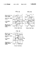
- FIG. 7 shows absorptivity when amorphous-phase recorded parts are already existent on the track of the optical recording medium of this invention and a temperature distribution of the track when the track is irradiated with a dc erasing laser having a constant power P 1 .
- numeral 1 indicates a heat inflow
- 2 indicates a heat outflow
- 3 indicates a recorded bit.
- the erasing power P 1 is a power to achieve an attainable temperature, in all the parts, of not lower than T m and not higher than T cool .
- the erasing power P 1 is a power to achieve an attainable temperature, in all the parts, of not lower than T m and not higher than T cool .
- the erasing power P 1 is a power to achieve an attainable temperature, in all the parts, of not lower than T m and not higher than T cool .
- the existing recorded parts to be erased have a smaller absorptivity, a distribution in which the attainable temperature of the recorded parts is lower than the attainable temperature of the unrecorded parts is obtained at temperatures of not lower than the melting point.
- the absorptivity of the existing recorded parts is larger, a distribution in which the attainable temperature of the recorded parts is higher than that of the unrecorded track is obtained.
- the heat flow formed on the track due to thermal conduction concentrates on the recorded part, which is to be erased, from the peripheral areas. That is, there is an effect to be heated by the heat flow from the unrecorded area in which the attainable temperature is higher than in the recorded area. Since the recorded part is gradually cooled even at a temperature of not higher than the melting point due to the higher attainable temperature area-rederived heat, crystalline nuclei occur inside the existing recorded part, and their number is large. The nuclei grow into crystals having fine particle sizes after solidification, and the existing recorded part is therefore crystallized, i.e., erased.
- the heat flow in an erasing medium is dispersed from the recorded part to be erased to unrecorded parts, and there is therefore no effect of the above gradual cooling.
- the recorded part There is rather a tendency to cool the recorded part rapidly, and the nuclei formation at a temperature around the melting point hardly takes place.
- the nuclei formation takes place, the nuclei occur in the unrecorded parts having a lower temperature, the number of nuclei occuring inside the existing recorded part is therefore very small, and the medium is cooled to room temperature before the crystalline growth, which occurs about the nucleus, preceeds sufficiently.
- the single beam overwrite stands for a recording and erasing method in which existing recorded signals on the track are erased and new signals are also recorded on the same track by the use of one round laser spot beam.
- the principal difference of this method from the above-specified erasion using a direct current light is found only in the case where a new signal is overwritten on the existing recorded part or a subpart thereof, and the erasing process, per se, is essentially identical between the single beam overwrite method and the direct current-applied erasing method.
- FIG. 9(a) and FIG. 9(b) show typical diagrams of overwrite-use laser power modulation, in which a recording power P 2 heats the recording film to a temperature of not lower than T cool , and at an overwriting time, overlaps a direct current bias power P 1 .
- the bias power has a power to melt an unrecorded part sufficiently.
- signals are overwritten by changing the pulse width tw and te.
- This invention achieves high erasability at an overwriting time.
- FIG. 10 shows an attainable temperature distribution on the track at an overwriting time where the existing recorded part to be erased (to be referred to as "old record” hereinbelow) and a new recording part (to be referred to as “new recording part” hereinbelow) are adjacent to each other.
- FIG. 11 shows said distribution where the old record and new recording part are completely apart from each other.
- FIGS. 12 and 13 show said distribution where the old record and new recording part are partially overlap each other.
- this invention makes it possible to achieve high erasability owing to the higher attainable temperature area-rederived heat effect.
- this invention has been able to show conventionally unknown high erasing performance not only at the time of a direct current irradiation and but also at the time of single beam overwriting.
- this invention has like effects even when the transmissivity of optical recording media is not zero.
- optical property of the optical recording media of this invention in which the reflectivity in the recorded state is rendered larger than that in the erased state or the absorptivity in the recorded state is rendered smaller than that in the erased state.
- the above optical property can be designed on the basis of the optical properties of a recording film, a dielectric film, a metal reflection film, etc., the thickness of each film, and the like.
- the constitutions of various media will be shown in Examples. An explanation here will be given with regard to the condition of the refractive index required to accomplish this invention.
- optical recording media in practical use is the limitation of the practical power of a laser source to be used for recording, reproducing and erasing.
- the recording film is melted.
- the recording film is sufficiently melted with a power in the range of practical-use laser power, i.e., not more than 15 mW on the surface of the film.
- This purpose is achieved either by using a recording film having a low melting point or by decreasing the film thickness so as to reduce the heat capacity of the recording film.
- the former procedure renders the recording film thermally unstable, and the crystallization temperature of the amorphous recorded part lowers together with the reduction of the melting point.
- the interference of a vertically incident beam is represented by the following equation.
- N (n 2 +k 2 )
- m is an integer of 1, 2, 3, . . . .
- the conditions of the refractive index and extinction coefficient of recording films are defined such that the reflectivity in the recorded state is larger than the reflectivity in the erased state at the first interference in not more than 80 nm at which the recording film can be sufficiently melted even in the range of practical laser powers.
- the reflectivity, transmissivity, absorptivity, refractive index and extinction coefficient were measured as follows.
- the reflectivity R (%) and transmissivity T (%) were measured by using a spectrophotometer. Samples were prepared by forming measurement-use materials having a predetermined thickness on a substrate sheet or substrate material having supporting property such as glass, or media having various structures were used as the sample.
- the energy reflectivity was measured by a method in which, by directing lights having a wavelength of 830 nm, obtained through a spectroscope, into a sample at an incident angle of 5°, reflected lights were integrated by means of an integrating sphere, and directed to a light detector.
- the energy transmissivity was measured by a method in which, by directing into a sample vertically from the sample surface side, lights transmitting the sample were integrated by means of an integrating sphere and directed to a light detector.
- the energy absorptivity A (%) can be calculated by the following equation based on the above R and T and the law of energy conservation.
- the refractive index and extinction coefficient were calculated on the basis of a measured energy reflectivity and transmissivity by using a computer simulation based on matrix calculation of multilayer system taking into account a multiple reflection in the interface (see A. Bell, et al., IEEE, J. Quntum Electron, page 487, 1987).
- optical disks were prepared by the sputtering method.
- a substrate 1.2 mm in thickness quartz glass, had glass, polycarbonate (PC) resin disks and polymethylmethacryl (PMMA) resin disks were used.
- PC polycarbonate
- PMMA polymethylmethacryl
- dielectric film SiN, AlN, SiO 2 , ZrO 2 , ZnS, Ta 2 O 5 , TiN, Cr 2 O 3 , GeN, TiO 2 , SiC, etc., were used (In this Example, the dielectric films are expressed by way of chemical formula having a chemical stoichiometric composition. However, the composition changes in actual use and it is difficult to obtain an exact composition).
- chromium, Ni-20% Cr alloy and aluminum were used for a metal reflection film. Films were formed by the RF sputtering method. The sputtering conditions were that the initial degree of vacuum was 8.5 ⁇ 10 -5 Pa; an RF output of 400 W and an Ar gas partial pressure of 1 mToor for dielectric films; an RF output of 200 W and an Ar gas partial pressure of 1 mToor for recording films; and a DC output of 200 W and an Ar gas partial pressure of 20 mTorr for metal reflection films. There is In 22 Te 37 Sb 41 (at %) as a recording material. By using this recording material, a film having the constitution of the optical recording medium was prepared, and the optical properties of the film were examined.
- this recording film composition has a refractive index n of 4.952 and an extinction coefficient k of 0.857 in the amorphous state, and a refractive index n of 4.678 and an extinction coefficient k of 1.743 in the crystalline state. That is, it is a characteristic of this invention that the refractive index is larger in the amorphous state than in the crystalline state.
- Table 1 summarizes the refractive indices n and extinction coefficients k of the compositions discussed in the section of prior art in the present specification. In any of the compositions, the refractive index is smaller in the amorphous state than in the crystalline state, which relationship is reverse to that of this invention.
- FIG. 15 shows an optical recording medium having a film constitution of substrate/recording film/dielectric, in which a recording film 9 was deposited up to a maximum thickness of 200 nm on a 1.2 mm glass substrate 8, and SiO 2 for a dielectric film 10 was deposited in the film thickness of 70 nm. A laser beam 11 was directed from the substrate side.
- FIG. 16(a) shows the optical properties of the above optical recording medium, in which its reflectivities in the recorded state (amorphous) and in the erased state (crystalline) are shown.
- FIG. 16(b) shows the absorptivities.
- the thicknesses of the recording film in which the reflectivity difference can be substantially detected are up to about 40 nm and between 90 nm and 130 nm, and the reflectivity is higher in the amorphous state than in the crystalline state.
- the absorptivities in all the range of thickness up to 200 nm are higher in the crystalline state than in the amorphous state as shown in FIG. 16(b). Therefore, the thickness of the recording film can be selected from the above-specified range.
- the film thickness increases, the heat capacity increases, the recording and erasing sensitivities with laser irradiation become poor, and a high-input laser is therefore necessary.
- FIG. 17 shows a film constitution of glass substrate/recording film/metal reflection film, in which the thickness of the metal reflection film 12 was constant or 100 nm, and the thickness of the recording film 9 was changed up to the maximum of 200 nm.
- FIG. 18(a) shows a case where gold was used for the metal reflection film 12, and the resultant medium with regard to the change of reflectivity in the amorphous state and crystalline state.
- the thickness of the recording film in which the reflectivity difference can be substantially detected is in the range of between 30 nm and 90 nm and between 130 nm and 170 nm. As shown in FIG.
- the absorptivity difference can be substantially detected when the thickness of the recording film is between about 30 nm and 80 nm and between about 130 nm and 160 nm.
- FIG. 19(a) and FIG. 19(b) show cases where chromium was used for the metal reflection film 12. Concerning the reflectivities, the reflectivity difference can be substantially detected when the film thickness is in the range of between about 40 nm and 80 nm and between 140 nm and 155 nm. Concerning the absorptivities, as shown in FIG. 19, the absorptivity difference can be substantially detected when the thickness of the recording film 9 is between about 40 nm and 80 nm, and about 150 nm.
- the reflectivity difference can be substantially detected when the thickness of the recording film 9 is between about 40 nm and 90 nm and between about 130 nm and 160 nm. As shown in FIG. 20(b), the absorptivity difference can be substantially detected when the thickness of the recording film is between about 40 nm and 80 nm, and about 154 nm.
- FIG. 21(a) and FIG. 21(b) show cases where Ni-20C R (wt. %) was used for the metal reflection film 12.
- reflectivity difference can be substantially detected when the thickness of the recording film 9 is between about 50 nm and 80 nm. As shown in FIG. 21(b), the absorptivity difference can be substantially detected in the range of between about 50 nm and 80 nm.
- FIG. 22 shows a film constitution of PC substrate/recording film/metal reflection film/dielectric film, in which gold having a thickness of 100 nm was used for the metal reflection film 12, SiN having a thickness of 80 nm was used for the dielectric film 10, and the thickness of the recording film 9 was changed up to the maximum of 200 nm.
- FIG. 23(a) shows changes of the reflectivities in the amorphous state and the crystalline state.
- the thickness of the recording film is between about 30 nm and 90 nm and between about 30 nm and 160 nm, in which ranges the reflection difference can be substantially detected.
- the absorptivity difference can be substantially detected when the thickness of the recording film is between about 30 nm and 80 nm and between 130 nm and 160 nm.
- FIG. 24(a) and FIG. 24(b) show a case of a film constitution of PMMA substrate/recording film/metal reflection film/dielectric film, in which chromium having a thickness of 100 nm was used for the metal reflection film 12, SiN having a thickness of 80 nm was used for the dielectric film 10, and the thickness of the recording film 9 was changed up to the maximum of 200 nm.
- FIG. 24(a) shows changes of the reflectivities in the amorphous state and crystalline state.
- the thickness of the recording film 9 is between about 40 nm and 80 nm and between about 130 nm and 170 nm. In these thicknesses, the reflection difference can be substantially detected. Concerning the absorptivity, as shown in FIG. 24(b), the absorptivity difference can be substantially detected when the thickness of the recording film 9 is between about 40 nm and 80 nm and in the vicinity of about 150 nm.
- FIG. 25(a) and FIG. 25(b) show a case of a film constitution of PMMA substrate/recording film/metal reflection film/dielectric film, in which aluminum having a thickness of 100 nm was used for the metal reflection film 12, SiN having a thickness of 80 nm was used for the dielectric film 10, and the thickness of the recording film 9 was changed up to the maximum of 200 nm.
- FIG. 25(a) shows changes of the reflectivities in the amorphous state and crystalline state.
- the thickness of the recording film 9 is between about 40 nm and 90 nm and in the vicinity of about 150 nm. In these thicknesses, the reflection difference can be substantially detected. Concerning the absorptivity, as shown in FIG. 25(b), the absorptivity difference can be substantially detected when the thickness of the recording film 9 is between about 40 nm and 90 nm and in the vicinity of about 150 nm.
- FIG. 26 shows a film constitution of glass substrate/recording film/dielectric film/metal reflection film, in which gold having a thickness of 60 nm was used for the metal reflection film 12, AlN having a thickness of 70 nm was used for the dielectric film 10, and the thickness of the recording film 9 was changed up to the maximum of 200 nm.
- FIG. 27(a) shows changes of the reflectivities in the amorphous state and crystalline state.
- the thickness of the recording film 9 is between about 10 nm and 65 nm and between about 105 and 140 nm. In these thickness, the reflection difference can be substantially detected. Concerning the absorptivity, as shown in FIG. 27(b), the absorptivity difference can be substantially detected when the thickness of the recording film 9 is between about 10 nm and 60 nm and between about 100 nm and 140 nm.
- FIG. 28 shows a film constitution of glass substrate/recording film/dielectric film/metal reflection film/dielectric film, in which gold having a thickness of 60 nm was used for the metal reflection film 12, AlN having a thickness of 70 nm was used for the dielectric film 10, and the thickness of the recording film 9 was changed up to the maximum of 200 nm.
- FIG. 29(a) shows changes of the reflectivities in the amorphous state and crystalline state.
- the thickness of the recording film 9 is between about 10 nm and 60 nm and between about 100 and 140 nm. In these thicknesses, the reflection difference can be substantially detected. Concerning the absorptivity, as shown in FIG. 29(b), the absorptivity difference can be substantially detected when the thickness of the recording film 9 is between about 10 nm and 70 nm and between about 100 nm and 140 nm.
- FIG. 30 shows a film constitution of PC substrate/dielectric film/recording film/dielectric film, in which AlN having a thickness of 70 nm was used for the dielectric film 10, and the thickness of the recording film 9 was changed up to the maximum of 200 nm.
- FIG. 31(a) shows changes of the reflectivities in the amorphous state and crystalline state.
- the thickness of the recording film 9 is between about 10 nm and 30 nm and between about 100 and 120 nm. In these thicknesses, the reflection difference can be substantially detected. Concerning the absorptivity, as shown in FIG. 31(b), the absorptivity difference can be substantially detected in all the range of thickness of the recording film 9.
- FIG. 32 shows a film constitution of PMMA substrate/dielectric film/recording film/metal reflection film, in which aluminum having a thickness of 100 nm was used for the metal reflection film 12, AlN having a thickness of 70 nm was used for the dielectric film 10, and the thickness of the recording film 9 was changed up to the maximum of 200 nm.
- FIG. 33(a) shows changes of the reflectivities in the amorphous state and crystalline state.
- the thickness of the recording film 9 is between about 20 nm and 80 nm and between about 130 and 160 nm. In these thicknesses, the reflection difference can be substantially detected. Concerning the absorptivity, as shown in FIG. 33(b), the absorptivity difference can be substantially detected when the thickness of the recording film 9 is between about 20 nm and 80 nm and between about 130 nm and 160 nm.
- FIG. 34(a) and FIG. 34(b) show a case of a film constitution of PC substrate/dielectric film/recording film/metal reflection film, in which gold having a thickness of 100 nm was used for the metal reflection film 12, AlN having a thickness of 70 nm was used for the dielectric film 10, and the thickness of the recording film 9 was changed up to the maximum of 200 nm.
- FIG. 34(a) shows changes of the reflectivities in the amorphous state and crystalline state.
- the thickness of the recording film 9 is between about 10 nm and 80 nm and between about 120 nm and 160 nm. In these thicknesses, the reflection difference can be substantially detected. Concerning the absorptivity, as shown in FIG. 34(b), the absorptivity difference can be substantially detected when the thickness of the recording film 9 is between about 10 nm and 80 nm and between about 120 nm and 160 nm.
- FIG. 35 shows a film constitution of glass substrate/dielectric film/recording film/metal reflection film/dielectric film, in which gold having a thickness of 100 nm was used for the metal reflection film 12, AlN having a thickness of 70 nm was used for the dielectric film 10, and the thickness of the recording film 9 was changed up to the maximum of 200 nm.
- FIG. 36(a) shows changes of the reflectivities in the amorphous state and crystalline state.
- the thickness of the recording film 9 is between about 10 nm and 80 nm and between about 120 and 160 nm. In these thicknesses, the reflection difference can be substantially detected. Concerning the absorptivity, as shown in FIG. 36(b), the absorptivity difference can be substantially detected when the thickness of the recording film 9 is between about 10 nm and 80 nm and between about 120 nm and 160 nm.
- FIG. 37(a) and FIG. 37(b) show a case of a film constitution of PC substrate/dielectric film/recording film/metal reflection film/dielectric film, in which aluminum having a thickness of 100 nm was used for the metal reflection film 12, AlN having a thickness of 70 nm was used for the dielectric film 10, and the thickness of the recording film 9 was changed up to the maximum of 200 nm.
- FIG. 37(a) shows changes of the reflectivities in the amorphous state and crystalline state.
- the thickness of the recording film 9 is between about 20 nm and 80 nm and between about 130 and 160 nm. In these thicknesses, the reflection difference can be substantially detected. Concerning the absorptivity, as shown in FIG. 37(b), the absorptivity difference can be substantially detected when the thickness of the recording film 9 is between about 20 nm and 85 nm and between about 130 nm and 160 nm.
- FIG. 38 shows a film constitution of PC substrate/dielectric film/recording film/dielectric film/metal reflection film, in which gold having a thickness of 100 nm was used for the metal reflection film 12, AlN having a thickness of 70 nm was used for the dielectric film 10, and the thickness of the recording film 9 was changed up to the maximum of 200 nm.
- FIG. 39(a) shows changes of the reflectivities in the amorphous state and crystalline state.
- the thickness of the recording film 9 1 is between about 10 nm and 70 nm and between about 90 and 150 nm. In these thicknesses, the reflection difference can be substantially detected. Concerning the absorptivity, as shown in FIG. 39(b), the absorptivity difference can be substantially detected when the thickness of the recording film 9 is between about 10 nm and 70 nm and between about 90 nm and 150 nm.
- FIG. 40(a) and FIG. 40(b) show a case of a film constitution of glass substrate/dielectric film/recording film/dielectric film/metal reflection film, in which aluminum having a thickness of 100 nm was used for the metal reflection film 12, AlN having a thickness of 70 nm was used for the dielectric film 10, and the thickness of the recording film 9 was changed up to the maximum of 200 nm.
- FIG. 40(a) shows changes of the reflectivities in the amorphous state and crystalline state.
- the thickness of the recording film 9 is between about 10 nm and 70 nm and between about 90 and 150 nm. In these thicknesses, the reflection difference can be substantially detected. Concerning the absorptivity, as shown in FIG. 40(b), the absorptivity difference can be substantially detected when the thickness of the recording film 9 is between about 10 nm and 70 nm and between about 70 nm and 150 nm.
- FIG. 41 shows a film constitution of PC substrate/dielectric film/recording film/dielectric film/metal reflection film/dielectric film, in which gold having a thickness of 100 nm was used for the metal reflection film 12, AlN having a thickness of 70 nm was used for the dielectric film 10, and the thickness of the recording film 9 was changed up to the maximum of 200 nm.
- FIG. 42(a) shows changes of the reflectivities in the amorphous state and crystalline state.
- the thickness of the recording film 9 is between about 10 nm and 70 nm and between about 90 and 150 nm. In these thicknesses, the reflection difference can be substantially detected. Concerning the absorptivity, as shown in FIG. 42(b), the absorptivity difference can be substantially detected when the thickness of the recording film 9 is between about 10 nm and 70 nm and between about 90 nm and 150 nm.
- FIG. 43(a) and FIG. 43(b) show a case of a film constitution of PC substrate/dielectric film/recording film/dielectric film/metal reflection film/dielectric film, in which aluminum having a thickness of 70 nm was used for the metal reflection film 12, AlN having a thickness of 70 nm was used for the dielectric film 10, and the thickness of the recording film 9 was changed up to the maximum of 200 nm.
- FIG. 43(a) shows changes of the reflectivities in the amorphous state and crystalline state.
- the thickness of the recording film 9 is between about 10 nm and 70 nm and between about 90 and 150 nm. In these thicknesses, the reflection difference can be substantially detected. Concerning the absorptivity, as shown in FIG. 43(b), the absorptivity difference can be substantially detected when the thickness of the recording film 9 is between about 10 nm and 70 nm and between about 70 nm and 150 nm.
- FIG. 44 shows a film constitution of glass substrate/recording film/glass substrate, in which the thickness of the recording film 9 was changed up to the maximum of 200 nm.
- FIG. 45(a) shows changes of the reflectivities in the amorphous state and crystalline state.
- the thickness of the recording film 9 is between about 10 nm and 60 nm and between about 100 and 150 nm. In these thicknesses, the reflection difference can be substantially detected. Concerning the absorptivity, as shown in FIG. 45(b), the absorptivity difference can be substantially detected when the thickness of the recording film 9 is between about 10 nm and 170 nm and between about 180 nm and 200 nm.
- FIG. 46 shows a film constitution of glass substrate/recording film/metal reflection film/glass substrate, in which gold having a thickness of 100 nm was used for the metal reflection film 12 and the thickness of the recording film 9 was changed up to the maximum of 200 nm.
- FIG. 47(a) shows changes of the reflectivities in the amorphous state and crystalline state.
- the thickness of the recording film 9 is between about 30 nm and 90 nm and between about 140 and 170 nm. In these thicknesses, the reflection difference can be substantially detected. Concerning the absorptivity, as shown in FIG. 47(b), the absorptivity difference can be substantially detected when the thickness of the recording film 9 is between about 30 nm and 90 nm and between about 130 nm and 160 nm.
- FIG. 48 shows a film constitution of PC substrate/SiN/recording film/Au/PC substrate, in which a gold having a thickness of 100 nm was used for the metal reflection film 12, SiN having a thickness of 70 nm was used for the dielectric film 10, and the thickness of the recording film 9 was changed up to the maximum of 200 nm.
- FIG. 49(a) shows changes of the reflectivities in the amorphous state and crystalline state.
- the thickness of the recording film 9 is between about 10 nm and 80 nm and between about 120 and 160 nm. In these thicknesses, the reflection difference can be substantially detected. Concerning the absorptivity, as shown in FIG. 49(b), the absorptivity difference can be substantially detected when the thickness of the recording film 9 is between about 10 nm and 80 nm and between about 120 nm and 160 nm.
- FIG. 50 shows a film constitution of PC substrate/SiN/recording film/Au/SiN/PC substrate, in which gold having a thickness of 100 nm was used for the metal reflection film 12, SiN having a thickness of 70 nm was used for the dielectric film 10, and the thickness of the recording film 9 was changed up to the maximum of 200 nm.
- FIG. 51(a) shows changes of the reflectivities in the amorphous state and crystalline state.
- the thickness of the recording film 9 is between about 10 nm and 80 nm and between about 120 and 160 nm. In these thicknesses, the reflection difference can be substantially detected. Concerning the absorptivity, as shown in FIG. 51(b), the absorptivity difference can be substantially detected when the thickness of the recording film 9 is between about 10 nm and 80 nm and between about 120 nm and 160 nm.
- FIG. 52 shows a film constitution of glass substrate/SiN/recording film/glass substrate, in which, SiN having a thickness of 70 nm was used for the dielectric film 10, and the thickness of the recording film 9 was changed up to the maximum of 200 nm.
- FIG. 53(a) shows changes of the reflectivities in the amorphous state and crystalline state.
- the thickness of the recording film 9 is between about 10 nm and 60 nm and between about 100 and 140 nm. In these thicknesses, the reflection difference can be substantially detected. Concerning the absorptivity, as shown in FIG. 53(b), the absorptivity difference can be substantially detected when the thickness of the recording film 9 is between about 10 nm and 200 nm.
- FIG. 54 shows a film constitution of PC substrate/SiN/recording film/SiN/PC substrate, in which SiN having a thickness of 70 nm was used for the dielectric film 10, and the thickness of the recording film 9 was changed up the maximum of 200 nm.
- FIG. 55(a) shows changes of the reflectivities in the amorphous state and crystalline state.
- the thickness of the recording film 9 is between about 10 nm and 50 nm and between about 80 and 140 nm. In these thicknesses, the reflection difference can be substantially detected. Concerning the absorptivity, as shown in FIG. 55(b), the absorptivity difference can be substantially detected when the thickness of the recording film 9 is between about 10 nm and 200 nm.
- FIG. 56 shows a film constitution of glass substrate/SiN/recording film/Au/glass substrate, in which gold having a thickness of 100 nm was used for the metal reflection film 12, SiN having a thickness of 70 nm was used for the dielectric film 10, and the thickness of the recording film 9 was changed up to the maximum of 200 nm.
- FIG. 57(a) shows changes of the reflectivities in the amorphous state and crystalline state.
- the thickness of the recording film 9 is between about 10 nm and 80 nm and between about 120 and 160 nm. In these thicknesses, the reflection difference can be substantially detected. Concerning the absorptivity, as shown in FIG. 57(b), the absorptivity difference can be substantially detected when the thickness of the recording film 9 is between about 10 nm and 80 nm and between about 120 nm and 160 nm.
- FIG. 58 shows a film constitution of PMMA substrate/SiN/recording film/Au/SiN/PMMA substrate, in which gold having a thickness of 100 nm was used for the metal reflection film 12, SiN having a thickness of 70 nm was used for the dielectric film 10, and the thickness of the recording film 9 was changed up to the maximum of 200 nm.
- FIG. 59(a) shows changes of the reflectivities in the amorphous state and crystalline state.
- the thickness of the recording film 9 is between about 10 nm and 90 nm and between about 120 and 160 nm. In these thicknesses, the reflection difference can be substantially detected. Concerning the absorptivity, as shown in FIG. 59(b), the absorptivity difference can be substantially detected when the thickness of the recording film 9 is between about 10 nm and 80 nm and between about 120 nm and 160 nm.
- FIG. 60 shows a film constitution of PC substrate/AlN/recording film/AlN/Au/PC substrate, in which gold having a thickness of 100 nm was used for the metal reflection film 12, AlN having a thickness of 70 nm was used for the dielectric film 10, and the thickness of the recording film 9 was changed up to the maximum of 200 nm.
- FIG. 61(a) shows changes of the reflectivities in the amorphous state and the crystalline state.
- the thickness of the recording film is between about 10 nm and 70 nm and between about 90 nm and 140 nm, in which ranges the reflection difference can be substantially detected.
- the absorptivity difference can be substantially detected when the thickness of the recording film 9 is between about 10 nm and 70 nm and between about 90 nm and 150 nm.
- FIG. 62(a) and FIG. 62(b) show a case of a film constitution of glass substrate/AlN/recording film/AlN/Ni-20 Cr/glass substrate, in which gold having a thickness of 100 nm was used for the metal reflection film 12, AlN having a thickness of 70 nm was used for the dielectric film 10, and the thickness of the recording film 9 was changed up to the maximum of 200 nm.
- FIG. 62(a) shows changes of the reflectivities in the amorphous state and crystalline state.
- the thickness of the recording film 9 is between about 10 nm and 70 nm and between about 90 nm and 150 nm. In these thicknesses, the reflection difference can be substantially detected. Concerning the absorptivity, as shown in FIG. 62(b), the absorptivity difference can be substantially detected when the thickness of the recording film 9 is between about 10 nm and 70 nm and between about 90 nm and 150 nm.
- FIG. 63(a) and FIG. 63(b) show a case of a film constitution of glass substrate/AlN/recording film/Al/glass substrate, in which Al having a thickness of 100 nm was used for the metal reflection film 12, AlN having a thickness of 70 nm was used for the dielectric film 10, and the thickness of the recording film 9 was changed up to the maximum of 200 nm.
- FIG. 63(a) shows changes of the reflectivities in the amorphous state and crystalline state.
- the thickness of the recording film 9 is between about 10 nm and 70 nm and between about 90 nm and 140 nm. In these thicknesses, the reflection difference can be substantially detected. Concerning the absorptivity, as shown in FIG. 63(b), the absorptivity difference can be substantially detected when the thickness of the recording film 9 is between about 10 nm and 70 nm and between about 90 nm and 150 nm.
- FIG. 64 shows a film constitution of PC substrate/AlN/recording film/AlN/Au/AlN/PC substrate, in which Au having a thickness of 100 nm was used for the metal reflection film 12, AlN having a thickness of 70 nm was used for the dielectric film 10, and the thickness of the recording film 9 was changed up to the maximum of 200 nm.
- FIG. 65(a) shows changes of the reflectivities in the amorphous state and crystalline state.
- the thickness of the recording film 9 is between about 10 nm and 60 nm and between about 90 nm and 140 nm. In these thicknesses, the reflection difference can be substantially detected. Concerning the absorptivity, as shown in FIG. 65(b), the absorptivity difference can be substantially detected when the thickness of the recording film 9 is between about 10 nm and 70 nm and between about 100 nm and 140 nm.
- FIG. 66(a) and FIG. 66(b) show a case of a film constitution of glass substrate/AlN/recording film/AlN/Cr/AlN/glass substrate, in which Cr having a thickness of 100 nm was used for the metal reflection film 12, AlN having a thickness of 70 nm was used for the dielectric film 10, and the thickness of the recording film 9 was changed up to the maximum of 200 nm.
- FIG. 66(a) shows changes of the reflectivities in the amorphous state and crystalline state.
- the thickness of the recording film 9 is between about 10 nm and 70 nm and between about 90 nm and 150 nm. In these thicknesses, the reflection difference can be substantially detected. Concerning the absorptivity, as shown in FIG. 66(b), the absorptivity difference can be substantially detected when the thickness of the recording film 9 is between about 10 nm and 70 nm and between about 90 nm and 140 nm.
- FIG. 67(a) and FIG. 67(b) show a case of a film constitution of glass substrate/AlN/recording film/AlN/Al/AlN/glass substrate, in which Al having a thickness of 100 nm was used for the metal reflection film 12, AlN having a thickness of 70 nm was used for the dielectric film 10, and the thickness of the recording film 9 was changed up to the maximum of 200 nm.
- FIG. 67(a) shows changes of the reflectives in the amorphous state and crystalline state.
- the thickness of the recording film 9 is between about 10 nm and 70 nm and between about 100 nm and 140 nm. In these thicknesses, the reflection difference can be substantially detected. Concerning the absorptivity, as shown in FIG. 67(b), the absorptivity difference can be substantially detected when the thickness of the recording film 9 is between about 10 nm and 70 nm and between about 100 nm and 140 nm.
- FIG. 68(a) and FIG. 68(b) show a case of a film constitution of PC substrate/AlN/recording film/AlN/Ni-20 Cr/AlN/PC substrate, in which Ni-20 Cr having a thickness of 100 nm was used for the metal reflection film 12, AlN having a thickness of 70 nm was used for the dielectric film 10, and the thickness of the recording film 9 was changed up to the maximum of 200 nm.
- FIG. 68(a) shows changes of the reflectivities in the amorphous state and crystalline state.
- the thickness of the recording film 9 is between about 10 nm and 60 nm and between about 100 nm and 140 nm. In these thicknesses, the reflection difference can be substantially detected. Concerning the absorptivity, as shown in FIG. 68(b), the absorptivity difference can be substantially detected when the thickness of the recording film 9 is between about 10 nm and 70 nm and between about 100 nm and 140 nm.
- FIG. 69 shows a film constitution of glass substrate/recording film/Au/glass substrate, in which gold having a thickness of 10 nm was used for the metal reflection film 12 and the thickness of the recording film 9 was changed up to the maximum of 200 nm.
- FIG. 70(a) shows changes of the reflectivities in the amorphous state and crystalline state.
- the thickness of the recording film 9 is between about 20 nm and 70 nm and between about 120 nm and 150 nm. In these thicknesses, the reflection difference can be substantially detected. Concerning the absorptivity, as shown in FIG. 70(b), the absorptivity difference can be substantially detected when the thickness of the recording film 9 is between about 10 nm and 160 nm.
- FIG. 71(a) and FIG. 71(b) show the reflectivity and absorptivity of a film using In 22 Sb 37 Te 41 (at %) of this invention and having a film constitution of glass substrate/dielectric film/recording film/dielectric film/metal reflection film/dielectric film when the dielectric film 10 positioned as a fourth layer from the glass substrate was changed up to 200 nm.
- Gold having a thickness of 100 nm was used for the metal reflection film 12, and SiO 2 having a thickness of 70 nm was used as the other dielectric films 10.
- FIG. 71(a) shows changes of the reflectivities in the amorphous state and crystalline state, and the reflection difference can be substantially detected in all the range of the thickness of the dielectric film 10. Further, concerning the absorptivity, as shown in FIG. 71(b), the absorptivity difference can be substantially detected in all the range of the thickness of the dielectric film 10 as well.
- FIG. 72(a) and FIG. 72(b) show the reflectivity and absorptivity of a film using In 22 Sb 37 Te 41 (at %) of this invention and having a film constitution of glass substrate/dielectric film/recording film/dielectric film/metal reflection film/dielectric film when the dielectric film 10 positioned as a second layer from the glass substrate was changed up to 200 nm.
- Gold having a thickness of 100 nm was used for the metal reflection film 12
- AlN having a thickness of 70 nm was used as the other dielectric films 10.
- FIG. 72(a) shows changes of the reflectivities in the amorphous state and crystalline state, and the reflection difference can be substantially detected in all the range of the thickness of the dielectric film 10. Further, concerning the absorptivity, as shown in FIG. 72(b), the absorptivity difference can be substantially detected in all the range of the thickness of the dielectric film 10 as well.
- FIG. 73(a) and FIG. 73(b) show a case where Se 52 Ge 27 Sn 21 (at %) was used as a recording material.
- the film constitution was PMMA substrate/dielectric film/recording film/dielectric film/metal reflection film/dielectric film, Gold having a thickness of 100 nm was used for the metal reflection film 12, ZrO 2 having a thickness of 70 nm was used as the dielectric films 10, and the thickness of the recording film 9 was changed up to the maximum of 200 nm.
- FIG. 73(a) shows changes of the reflectivities in the amorphous state and crystalline state, and the reflection difference can be substantially detected when the thickness of the recording film 9 is between about 10 nm and 80 nm and between about 100 nm and 180 nm. Further, concerning the absorptivity, as shown in FIG. 73(b), the absorptivity difference can be substantially detected when the thickness of the recording film 9 is between about 10 nm and 80 nm and between about 100 nm and 180 nm.
- FIG. 74(a) and FIG. 74(b) show a case where Sb 56 Se 40 Zn 4 (at %) was used as a recording material
- the film constitution was PC substrate/dielectric film/recording film/dielectric film/metal reflection film/dielectric film, Gold having a thickness of 100 nm was used for the metal reflection film 12, ZrO 2 having a thickness of 70 nm was used as the dielectric films 10, and the thickness of the recording film 9 was changed up to the maximum of 200 nm.
- FIG. 74(a) shows changes of the reflectivities in the amorphous state and crystalline state, and the reflection difference can be substantially detected when the thickness of the recording film 9 is between about 10 nm and 80 nm and between about 110 nm and 120 nm. Further, concerning the absorptivity, as shown in FIG. 74(b), the absorptivity difference can be substantially detected when the thickness of the recording film 9 is between about 10 nm and 80 nm and between about 100 nm and 180 nm.
- FIG. 75(a) and FIG. 75(b) show a case where Sb 34 Se 58 Sn 8 (at %) was used as a recording material
- the film constitution was PC substrate/dielectric film/recording film/dielectric film/metal reflection film/dielectric film, Gold having a thickness of 100 nm was used for the metal reflection film 12, AlN having a thickness of 70 nm was used as the dielectric films 10, and the thickness of the recording film 9 was changed up to the maximum of 200 nm.
- FIG. 75(a) shows changes of the reflectivities in the amorphous state and crystalline state, and the reflection difference can be substantially detected in all the range of the thickness of the recording film 9 Further, concerning the absorptivity, as shown in FIG. 75(b), the absorptivity difference can be substantially detected in all the range of the thickness of the recording film 9 as well.
- FIG. 76(a) and FIG. 76(b) show a case where Sb 64 Se 29 Zn 27 (at %) was used as a recording material
- the film constitution was PMMA substrate/dielectric film/recording film/dielectric film/metal reflection film/dielectric film, gold having a thickness of 100 nm was used for the metal reflection film 12, SiN having a thickness of 70 nm was used as the dielectric films 10, and the thickness of the recording film 9 was changed up to the maximum of 200 nm.
- FIG. 76(a) shows changes of the reflectivities in the amorphous state and crystalline state, and the reflection difference can be substantially detected in all the range of the thickness of the recording film 9 Further, concerning the absorptivity, as shown in FIG. 76(b), the absorptivity difference can be substantially detected in all the range of the thickness of the recording film 9 as well.
- FIG. 77(a) and FIG. 77(b) show a case where Te 64 Sb 6 Sn 30 (at %) was used as a recording material
- the film constitution was PMMA substrate/dielectric film/recording film/dielectric film/metal reflection film/dielectric film, Gold having a thickness of 100 nm was used for the metal reflection film 12, AlN having a thickness of 70 nm was used as the dielectric films 10, and the thickness of the recording film 9 was changed up to the maximum of 200 nm.
- FIG. 77(a) shows changes of the reflectivities in the amorphous state and crystalline state, and the reflection difference can be substantially detected in all the range of the thickness of the recording film 9 Further, concerning the absorptivity, as shown in FIG. 77(b), the absorptivity difference can be substantially detected in all the range of the thickness of the recording film 9 as well.
- FIG. 78(a) and FIG. 78(b) show an embodiment of recording and erasing with regard to rewritable disks using optical recording media.
- the disks were prepared according to a high frequency sputtering method which comprises depositing 70 nm to 80 nm thick AlN for an optical interference film on 5.25 inch glass substrates having a laser guide groove for laser beam tracking of the continuous-servo tracking technique, 30 nm to 50 nm thick In 22 Sb 37 Te 41 for a recording film thereon, 70 to 80 nm thick AlN thereon, 100 nm thick Au for an optical reflection film thereon, and 100 nm thick AlN for a protective film thereon.
- the above recorded track was irradiated with a direct current beam having the same power of 13 mW as that in the recording, to show that the recorded signal was erased down to 5 dB on a spectrum analyzer shown in FIG. 78(b).
- the erasability is -45 dB, which is above the practical-use level although the irradiation power was the same.
- this invention gives high erasing performance even in a recording and erasing method unthinkable with regard to conventional optical recording media.
- resin substrates such as PMMA, PC, etc.
- FIG. 79(a) and FIG. 79(b) show an embodiment of the single beam overwrite with regard to rewritable optical disks using the optical recording medium of this invention.
- the disk constitution was the same as that of the above embodiment.
- FIG. 79(a) shows a power modulation mode of a round laser spot beam (spot diameter: about 1.5 ⁇ m) used for the overwriting.
- a recording power P 1 which can heat a recording film to a temperature of not less than T cool
- a bias power P 2 which can heat the recording film to a temperature of between not less than the melting point and not more than T cool
- the ratios of P 1 /P 2 12.5 mW/9.5 mW and 16 mW/12 mW were selected.
- the disks were turned at 1,800 to 2,400 rounds/minute, and continuously irradiated with a 15 mW direct current beam to reduce the disk reflectivity from about 50% to about 20%, whereby recording track portion was formed. Then, sine wave signals having a modulated frequency of 2 MHz were recorded by irradiation of a laser having the above power, and thereafter, 3 MHz sine wave signals were recorded by overwriting the 2 MHz signals. As shown in FIG. 79(a) and FIG.
- the spectrum analyzer showed that the 2 MHz signals recorded in a C/N equivalent to 50 dB were erased to an equivalence of 2 dB by the overwrite-recorded 3 MHz signals, and at the same time it was shown that the 3 MHz signals were overwrite-recorded in a C/N equivalent to 50 dB. In a process reverse thereto, similar results were obtained. It has been demonstrated that this invention can give erasing performance in the single beam overwrite, found in no prior art, that the erasability is -45 dB or more. Further, the number of repeatable times for the above overwrite was examined. As shown in FIG. 80(a) and FIG. 80(b), the overwrite of 2 MHz and 3 MHz sine wave signals with both of the laser powers could be repeated more than 10 5 times while the erasability was -35 dB or more.
- FIG. 81(a) and FIG. 81(b) show 2 MHz sine wave signals on an oscilloscope screen. Any deformation of waveforms and change of frequency due to incomplete erasion wave recognized in any of the signals, and the signals were completely erased in both the cases. It has been demonstrated that the optical recording media of this invention make it possible to perform the single beam overwrite free from incomplete erasion even with a practical-use laser power of 15 mW or less. And when resin substrates such as PMMA, PC, etc., were used as the substrate, it was also possible to obtain results identical with those of the above embodiment. Further, in the case of using disks according to another tracking system, sampled-servo tracking technique, the optical recording media of this invention were also able to give the same results as those of the above embodiment.
- the recording films described in Table 2 constitute the optical recording media which have a larger reflectivity, n, in the amorphous state than in the crystalline state and actually satisfy the changes therein are different from those in the conventional materials described in Table 1.
- the recording films comprises a compound of simple substances of elements such as antimony, zinc, tin, germanium, etc., with of selenium, tellurium, etc.
- the simple substance of elements indium, lead, silver, copper, gold, etc., are also effective to control the refractive index of the recording film.
- Table 3 shows the recordability and erasability of optical disks having the recording films described in Table 2.
- the disks were prepared according to the high frequency sputtering method which comprises depositing 70 nm to 80 nm thick AlN, for an optical interference film, on a 5.25 inch glass substrate having a laser guide groove for laser beam tracking of continuous servo technique, 330 nm to 50 nm thick recording material selected from the recording films described in Table 2 thereon, 100 nm thick Au for an optical reflection film thereon and 100 nm thick AlN for a protective film thereon.
- the recording power and erasing power were 15 mW or less.
- optical disks gave a C/N of about 50 dB and were of high sensitivity, and further, these optical disks were able to give a high erasability of -35 dB or more in both the direct current and overwrite erasing methods.
- the recording media gave high-sensitivity recording and high erasability, and there is no special limitation to be imposed on the wavelength for use.
- optical recording media satisfying the reflectivity and absorptivity in the as-deposited state and the reflectivity and absorptivity in the recorded and erased states, a track having a lower reflectivity (often equivalent to the reflectivity in the erased state) than that in the as-deposited state is first formed, and signals are recorded on the track.
- the other portion (outside the track and corresponding to a groove of a disk for the continuous servo technique) is that which has a higher reflectivity (or a lower absorptivity) and remains in the as-deposited state.
- the cross-talk increase in the minimizing of the intertrack distance determines the recording density on the optical recording media.
- the outside-the-track portion having a smaller reflectivity and being in the as-deposited state is positioned in contact with the track portion.
- the outside-the-track portion is less influenced thermally by a laser power used for the recording and erasing on the track portion, since its attainable temperature is low.
- the cross-talk to an adjacent track is reduced especially by this thermal block.
- the cross-talk is as small as -40 dB or less, which value is very small as compared with conventional ones.
- the relationship in the reflectivities or absorptivities is reverse to that in this invention, and the outside-the-track portion is therefore likely to be thermally influenced.
- the above effect can be produced only by the optical recording media of this invention, and it is made possible to perform the recording in an unconventionally higher density.
- FIG. 83 is a block diagram of a unit showing a process for optical information recording and reproducing as one embodiment of this invention.
- the unit comprises an optical pickup 13, an optical pickup position control circuit 14, a received signal processing circuit 15, a laser diode actuating circuit 16, a disk-turning motor 17, a turn table 18, an optical disk 19 with a tracking guide, a melting point discrimination processing portion 20 for the recording film of an optical disk, a system control circuit 21, and a set of external input-output terminals 22.
- the optical disk has a constitution in which a 70 nm thick AlN film is sputtering-formed on a glass substrate, a 50 nm thin film of In-Sb-Te type as a recording film is sputtering-formed thereon, a 70 nm thick AlN film is again sputtering-formed thereon, a 100 nm thick Au film is further sputtering-formed thereon, a 100 nm thick AlN film as a protective film is formed thereon, and a 10 ⁇ m thick UV-hardening resin film as a protective film is finally spin-coated thereon.
- the above optical disk 19 is placed on the turn table 18, and the motor 17 turns the turn table 18 to turn the optical disk 19.
- the turning is switched on or off through the external input-output terminals 21 via the system control circuit 21.
- the optical disk 19 is irradiated with a laser beam 23 from the optical pickup 13.
- a reflected beam portion of the laser beam 23 returns to the optical pickup 13 to extract an optical pickup height signal and deflection signal on the track through the received signal processing circuit 15.
- the optical pickup position control circuit 14 controls the focusing and tracking of the optical pickup 13 on the disk 19.
- the focusing and tracking are switched on or off through the external input-output terminals 22 via the system control circuit 21.
- the optical pickup 13 has a constitution such that the system control circuit 21 sets a laser irradiation power as required in keeping with the passage of time through the laser diode actuating circuit 16 whereby the overwrite is possible by using one beam.
- a laser irradiation power necessary to heat the optical disk 19 to a temperature of its melting point or more is written in a control track provided in the inner or outer circumference of the optical disk 19, and at the time of overwriting, the melting point discrimination processing portion 20 sets the recording point irradiation power and erasing point irradiation power at a power necessary to heat to the melting point or more.
- the melting point discrimination processing portion 20 can read the above written data to overwrite at a temperature of the melting point or more, or a power P M for heating to the melting point may be determined on the basis of reflectivity changes obtained while effecting a laser irradiation by using a dummy track as follows.
- this invention provides recording media having high erasing performance and high density redordability which the conventional ones do not have and information recording and reproducing units.
Priority Applications (2)
| Application Number | Priority Date | Filing Date | Title |
|---|---|---|---|
| US08/205,768 US5484686A (en) | 1988-06-24 | 1994-03-04 | Optical recording media and information recording and reproducing units |
| US09/008,847 USRE36624E (en) | 1988-06-24 | 1998-01-15 | Optical recording media and information recording and reproducing units |
Applications Claiming Priority (5)
| Application Number | Priority Date | Filing Date | Title |
|---|---|---|---|
| JP63-154743 | 1988-06-24 | ||
| JP63154743A JP2512087B2 (ja) | 1988-06-24 | 1988-06-24 | 光記録媒体および光記録方法 |
| US36687389A | 1989-06-15 | 1989-06-15 | |
| US91766492A | 1992-07-20 | 1992-07-20 | |
| US08/205,768 US5484686A (en) | 1988-06-24 | 1994-03-04 | Optical recording media and information recording and reproducing units |
Related Parent Applications (1)
| Application Number | Title | Priority Date | Filing Date |
|---|---|---|---|
| US91766492A Continuation | 1988-06-24 | 1992-07-20 |
Related Child Applications (1)
| Application Number | Title | Priority Date | Filing Date |
|---|---|---|---|
| US09/008,847 Reissue USRE36624E (en) | 1988-06-24 | 1998-01-15 | Optical recording media and information recording and reproducing units |
Publications (1)
| Publication Number | Publication Date |
|---|---|
| US5484686A true US5484686A (en) | 1996-01-16 |
Family
ID=15590945
Family Applications (2)
| Application Number | Title | Priority Date | Filing Date |
|---|---|---|---|
| US08/205,768 Ceased US5484686A (en) | 1988-06-24 | 1994-03-04 | Optical recording media and information recording and reproducing units |
| US09/008,847 Expired - Lifetime USRE36624E (en) | 1988-06-24 | 1998-01-15 | Optical recording media and information recording and reproducing units |
Family Applications After (1)
| Application Number | Title | Priority Date | Filing Date |
|---|---|---|---|
| US09/008,847 Expired - Lifetime USRE36624E (en) | 1988-06-24 | 1998-01-15 | Optical recording media and information recording and reproducing units |
Country Status (7)
| Country | Link |
|---|---|
| US (2) | US5484686A (zh) |
| EP (2) | EP0347801B1 (zh) |
| JP (1) | JP2512087B2 (zh) |
| KR (1) | KR0144001B1 (zh) |
| CN (1) | CN1018303B (zh) |
| CA (1) | CA1332467C (zh) |
| DE (2) | DE68929438T2 (zh) |
Cited By (12)
| Publication number | Priority date | Publication date | Assignee | Title |
|---|---|---|---|---|
| US5811217A (en) * | 1991-07-24 | 1998-09-22 | Matsushita Electric Industrial Co., Ltd. | Optical information recording medium and optical information recording/reproducing method |
| US5889756A (en) * | 1996-07-25 | 1999-03-30 | Kabushiki Kaisha Toshiba | Phase change optical recording medium |
| US6268034B1 (en) | 1998-08-05 | 2001-07-31 | Matsushita Electric Industrial Co., Ltd. | Optical information recording medium and method for producing the same, method for recording and reproducing information thereon and recording/reproducing apparatus |
| US6343062B1 (en) | 1997-09-26 | 2002-01-29 | Matsushita Electric Industrial Co., Ltd | Optical disk device and optical disk for recording and reproducing high-density signals |
| US6388984B2 (en) | 1997-08-28 | 2002-05-14 | Matsushita Electric Industrial Co., Ltd. | Optical information recording medium and its recording and reproducing method |
| US20030003395A1 (en) * | 2001-02-28 | 2003-01-02 | Ricoh Company, Ltd. | Phase-change optical recording medium |
| US6503690B1 (en) | 1997-08-12 | 2003-01-07 | Matsushita Electric Industrial Co., Ltd. | Optical information recording medium, method for producing the same, and method for recording and reproducing optical information |
| US20030076775A1 (en) * | 2000-11-06 | 2003-04-24 | Shuji Sato | Optical recording medium, optical recording medium production method, optical recording medium production apparatus, program, and medium |
| US20040213121A1 (en) * | 2001-11-27 | 2004-10-28 | Tdk Corp. | Optical recording medium and optical recording method |
| US6821707B2 (en) * | 1996-03-11 | 2004-11-23 | Matsushita Electric Industrial Co., Ltd. | Optical information recording medium, producing method thereof and method of recording/erasing/reproducing information |
| US20080030969A1 (en) * | 2006-07-19 | 2008-02-07 | Samsung Electro-Mechanics Co., Ltd. | Method for manufacturing a printed circuit board with a thin film capacitor embedded therein having a dielectric film by using laser lift-off, and printed circuit board with a thin film capacitor embedded therein manufactured thereby |
| USRE47382E1 (en) * | 2005-07-18 | 2019-05-07 | Xenogenic Development Limited Liability Company | Back-to-back metal/semiconductor/metal (MSM) Schottky diode |
Families Citing this family (17)
| Publication number | Priority date | Publication date | Assignee | Title |
|---|---|---|---|---|
| US5291470A (en) * | 1988-03-28 | 1994-03-01 | Matsushita Electric Industrial Co., Ltd. | Optical information recording method |
| JP2538647B2 (ja) * | 1988-07-22 | 1996-09-25 | 富士通株式会社 | 光ディスク媒体 |
| JPH02249136A (ja) * | 1989-03-23 | 1990-10-04 | Asahi Chem Ind Co Ltd | 光学的記録再生装置 |
| DE4019301A1 (de) * | 1990-06-16 | 1991-12-19 | Basf Ag | Reversibler optischer aufzeichnungstraeger vom phasenwechsel-typ |
| JP2750018B2 (ja) * | 1990-07-13 | 1998-05-13 | インターナショナル・ビジネス・マシーンズ・コーポレイション | 光学記録媒体及び光学データ記録ディスクドライブシステム |
| US5242784A (en) * | 1990-07-13 | 1993-09-07 | International Business Machines Corporation | System and method for optical phase change recording |
| JP2556183B2 (ja) * | 1990-09-11 | 1996-11-20 | 富士ゼロックス株式会社 | 光学的記録方法とこの方法を用いる光記録媒体 |
| JP2987223B2 (ja) * | 1991-02-20 | 1999-12-06 | ティーディーケイ株式会社 | 光記録媒体 |
| DE69317459T2 (de) * | 1992-04-17 | 1998-08-27 | Matsushita Electric Ind Co Ltd | Optisches Informationsaufzeichnungsmedium und Verfahren zum Entwurf seiner Struktur |
| JPH0778354A (ja) * | 1993-09-07 | 1995-03-20 | Toshiba Corp | 情報記録媒体およびそれを用いた記録方法 |
| JP2806274B2 (ja) * | 1994-10-19 | 1998-09-30 | 日本電気株式会社 | 光学情報記録媒体 |
| CN1054227C (zh) * | 1994-10-31 | 2000-07-05 | 北京航空航天大学 | 记录媒体及其记录和擦除方法 |
| US6798711B2 (en) * | 2002-03-19 | 2004-09-28 | Micron Technology, Inc. | Memory with address management |
| JP2005174528A (ja) | 2003-11-18 | 2005-06-30 | Hitachi Maxell Ltd | 光ディスク及びその製造方法並びに記録再生装置 |
| JP4576316B2 (ja) | 2005-10-20 | 2010-11-04 | 株式会社日立製作所 | サーボ制御信号生成装置、光ディスク装置及びサーボ制御信号生成方法 |
| TWI402829B (zh) * | 2010-10-29 | 2013-07-21 | Nat Univ Tsing Hua | 多階記錄方法及其系統 |
| KR102383501B1 (ko) * | 2015-01-08 | 2022-04-07 | 삼성전자주식회사 | 다층 박막, 그 제조 방법 및 이를 포함하는 전자 제품 |
Citations (13)
| Publication number | Priority date | Publication date | Assignee | Title |
|---|---|---|---|---|
| GB2079031A (en) * | 1980-05-14 | 1982-01-13 | Rca Corp | Optical information record and a method of reversibly recording and erasing information thereon |
| US4460636A (en) * | 1981-03-27 | 1984-07-17 | Sony Corporation | Optical information record member |
| CA1193008A (en) * | 1979-03-12 | 1985-09-03 | Craig I. Willis | Information-recording process and apparatus |
| EP0186329A2 (en) * | 1984-11-29 | 1986-07-02 | Hitachi, Ltd. | Information recording medium |
| US4629649A (en) * | 1984-12-28 | 1986-12-16 | Tdk Corporation | Information recording medium and method |
| US4645712A (en) * | 1984-11-09 | 1987-02-24 | Hitachi, Ltd. | Information recording medium |
| US4670345A (en) * | 1985-02-22 | 1987-06-02 | Asahi Kasei Kogyo Kabushiki Kaisha | Information recording medium |
| EP0243976A2 (en) * | 1986-05-02 | 1987-11-04 | Hitachi, Ltd. | Method for recording, reproducing and erasing information and thin film for recording information |
| US4710899A (en) * | 1985-06-10 | 1987-12-01 | Energy Conversion Devices, Inc. | Data storage medium incorporating a transition metal for increased switching speed |
| EP0286406A2 (en) * | 1987-04-08 | 1988-10-12 | Hitachi, Ltd. | Optical recording medium |
| US4787077A (en) * | 1985-08-15 | 1988-11-22 | International Business Machines Corporation | Process for optically storing information using materials having a single phase in both the crystalline state and the amorphous state |
| EP0319037A2 (en) * | 1987-12-04 | 1989-06-07 | Matsushita Electric Industrial Co., Ltd. | Optical information recording medium |
| US4975355A (en) * | 1987-01-30 | 1990-12-04 | Kabushiki Kaisha Toshiba | Information storage medium |
Family Cites Families (15)
| Publication number | Priority date | Publication date | Assignee | Title |
|---|---|---|---|---|
| US3716844A (en) * | 1970-07-29 | 1973-02-13 | Ibm | Image recording on tetrahedrally coordinated amorphous films |
| US3971874A (en) * | 1973-08-29 | 1976-07-27 | Matsushita Electric Industrial Co., Ltd. | Optical information storage material and method of making it |
| US4330833A (en) * | 1978-05-26 | 1982-05-18 | Vicom Systems, Inc. | Method and apparatus for improved digital image processing |
| JPS59185048A (ja) * | 1983-04-01 | 1984-10-20 | Matsushita Electric Ind Co Ltd | 光学情報記録部材及び記録方法 |
| KR860002121B1 (ko) * | 1984-03-28 | 1986-11-26 | 마쓰시다덴기산교 가부시기가이샤 | 광학정보 기록부재 |
| JPS60231928A (ja) * | 1984-04-27 | 1985-11-18 | Matsushita Electric Ind Co Ltd | 光学情報記録消去方法 |
| KR890004230B1 (ko) * | 1984-08-24 | 1989-10-27 | 가부시끼가이샤 도오시바 | 광(光) 디스크 메모리 |
| JPS6196541A (ja) * | 1984-10-18 | 1986-05-15 | Nec Corp | 光磁気記録媒体 |
| JPS61210538A (ja) * | 1985-03-14 | 1986-09-18 | Victor Co Of Japan Ltd | 記録媒体用インジウム−ニオビウム合金 |
| JPH0734267B2 (ja) * | 1985-05-24 | 1995-04-12 | 松下電器産業株式会社 | 可逆的光学情報記録媒体および記録再生方法 |
| JPS6286553A (ja) * | 1985-10-11 | 1987-04-21 | Matsushita Electric Ind Co Ltd | 光学情報記録部材 |
| US4818666A (en) * | 1986-03-28 | 1989-04-04 | U.S. Philips Corporation | Erasable optical recording element and method of optically recording and erasing information |
| JPS63188836A (ja) * | 1987-01-30 | 1988-08-04 | Sanyo Electric Co Ltd | 光学記録媒体 |
| DE3705389A1 (de) * | 1987-02-20 | 1988-09-01 | Basf Ag | Substituierte crotonsaeureester und diese enthaltende fungizide |
| JPH01165043A (ja) * | 1987-12-21 | 1989-06-29 | Fuji Electric Co Ltd | 光記録媒体 |
-
1988
- 1988-06-24 JP JP63154743A patent/JP2512087B2/ja not_active Expired - Fee Related
-
1989
- 1989-06-13 CA CA000602705A patent/CA1332467C/en not_active Expired - Fee Related
- 1989-06-19 DE DE68929438T patent/DE68929438T2/de not_active Expired - Fee Related
- 1989-06-19 EP EP89111107A patent/EP0347801B1/en not_active Expired - Lifetime
- 1989-06-19 EP EP97104514A patent/EP0784316B1/en not_active Expired - Lifetime
- 1989-06-19 DE DE68928337T patent/DE68928337T2/de not_active Expired - Fee Related
- 1989-06-23 KR KR1019890008701A patent/KR0144001B1/ko not_active IP Right Cessation
- 1989-06-24 CN CN89106296A patent/CN1018303B/zh not_active Expired
-
1994
- 1994-03-04 US US08/205,768 patent/US5484686A/en not_active Ceased
-
1998
- 1998-01-15 US US09/008,847 patent/USRE36624E/en not_active Expired - Lifetime
Patent Citations (13)
| Publication number | Priority date | Publication date | Assignee | Title |
|---|---|---|---|---|
| CA1193008A (en) * | 1979-03-12 | 1985-09-03 | Craig I. Willis | Information-recording process and apparatus |
| GB2079031A (en) * | 1980-05-14 | 1982-01-13 | Rca Corp | Optical information record and a method of reversibly recording and erasing information thereon |
| US4460636A (en) * | 1981-03-27 | 1984-07-17 | Sony Corporation | Optical information record member |
| US4645712A (en) * | 1984-11-09 | 1987-02-24 | Hitachi, Ltd. | Information recording medium |
| EP0186329A2 (en) * | 1984-11-29 | 1986-07-02 | Hitachi, Ltd. | Information recording medium |
| US4629649A (en) * | 1984-12-28 | 1986-12-16 | Tdk Corporation | Information recording medium and method |
| US4670345A (en) * | 1985-02-22 | 1987-06-02 | Asahi Kasei Kogyo Kabushiki Kaisha | Information recording medium |
| US4710899A (en) * | 1985-06-10 | 1987-12-01 | Energy Conversion Devices, Inc. | Data storage medium incorporating a transition metal for increased switching speed |
| US4787077A (en) * | 1985-08-15 | 1988-11-22 | International Business Machines Corporation | Process for optically storing information using materials having a single phase in both the crystalline state and the amorphous state |
| EP0243976A2 (en) * | 1986-05-02 | 1987-11-04 | Hitachi, Ltd. | Method for recording, reproducing and erasing information and thin film for recording information |
| US4975355A (en) * | 1987-01-30 | 1990-12-04 | Kabushiki Kaisha Toshiba | Information storage medium |
| EP0286406A2 (en) * | 1987-04-08 | 1988-10-12 | Hitachi, Ltd. | Optical recording medium |
| EP0319037A2 (en) * | 1987-12-04 | 1989-06-07 | Matsushita Electric Industrial Co., Ltd. | Optical information recording medium |
Non-Patent Citations (2)
| Title |
|---|
| Akahira et al, SPIE vol. 899, pp. 188 195, 1988 Optical Storage Technology and Applications. * |
| Akahira et al, SPIE vol. 899, pp. 188-195, 1988 Optical Storage Technology and Applications. |
Cited By (21)
| Publication number | Priority date | Publication date | Assignee | Title |
|---|---|---|---|---|
| US5811217A (en) * | 1991-07-24 | 1998-09-22 | Matsushita Electric Industrial Co., Ltd. | Optical information recording medium and optical information recording/reproducing method |
| US7037413B1 (en) | 1996-03-11 | 2006-05-02 | Matsushita Electric Industrial Co., Ltd. | Optical information recording medium, producing method thereof and method of recording/erasing/reproducing information |
| US6821707B2 (en) * | 1996-03-11 | 2004-11-23 | Matsushita Electric Industrial Co., Ltd. | Optical information recording medium, producing method thereof and method of recording/erasing/reproducing information |
| US20050089799A1 (en) * | 1996-03-11 | 2005-04-28 | Matsushita Electric Industrial Co., Ltd. | Optical information recording medium, producing method thereof and method of recording/erasing/reproducing information |
| US5889756A (en) * | 1996-07-25 | 1999-03-30 | Kabushiki Kaisha Toshiba | Phase change optical recording medium |
| US6503690B1 (en) | 1997-08-12 | 2003-01-07 | Matsushita Electric Industrial Co., Ltd. | Optical information recording medium, method for producing the same, and method for recording and reproducing optical information |
| US6388984B2 (en) | 1997-08-28 | 2002-05-14 | Matsushita Electric Industrial Co., Ltd. | Optical information recording medium and its recording and reproducing method |
| US6343062B1 (en) | 1997-09-26 | 2002-01-29 | Matsushita Electric Industrial Co., Ltd | Optical disk device and optical disk for recording and reproducing high-density signals |
| US6268034B1 (en) | 1998-08-05 | 2001-07-31 | Matsushita Electric Industrial Co., Ltd. | Optical information recording medium and method for producing the same, method for recording and reproducing information thereon and recording/reproducing apparatus |
| US20070223354A1 (en) * | 2000-11-06 | 2007-09-27 | Matsushita Electric Industrial Co., Ltd. | Optical recording medium, method of manufacturing optical recording medium, apparatus for manufacturing optical recording medium, program, and medium |
| US20030076775A1 (en) * | 2000-11-06 | 2003-04-24 | Shuji Sato | Optical recording medium, optical recording medium production method, optical recording medium production apparatus, program, and medium |
| US7239601B2 (en) | 2000-11-06 | 2007-07-03 | Matsushita Electric Industrial Co., Ltd. | Optical recording medium, method of manufacturing optical recording medium, apparatus for manufacturing optical recording medium, program, and medium |
| US6846611B2 (en) * | 2001-02-28 | 2005-01-25 | Ricoh Company, Ltd. | Phase-change optical recording medium |
| US20030003395A1 (en) * | 2001-02-28 | 2003-01-02 | Ricoh Company, Ltd. | Phase-change optical recording medium |
| US20040213121A1 (en) * | 2001-11-27 | 2004-10-28 | Tdk Corp. | Optical recording medium and optical recording method |
| USRE47382E1 (en) * | 2005-07-18 | 2019-05-07 | Xenogenic Development Limited Liability Company | Back-to-back metal/semiconductor/metal (MSM) Schottky diode |
| US20080030969A1 (en) * | 2006-07-19 | 2008-02-07 | Samsung Electro-Mechanics Co., Ltd. | Method for manufacturing a printed circuit board with a thin film capacitor embedded therein having a dielectric film by using laser lift-off, and printed circuit board with a thin film capacitor embedded therein manufactured thereby |
| US20090223706A1 (en) * | 2006-07-19 | 2009-09-10 | Samsung Electro-Mechanics Co.,Ltd | Method for manufacturing a printed circuit board with a thin film capacitor embedded therein having a dielectric film by using laser lift-off, and printed circuit board with a thin film capacitor embedded therein manufactured thereby |
| US20090223045A1 (en) * | 2006-07-19 | 2009-09-10 | Samsung Electro-Mechanics Co., Ltd. | Method for manufacturing a printed circuit board with a thin film capacitor embedded therein having a dielectric film by using laser lift-off, and printed circuit board with a thin film capacitor embedded therein manufactured thereby |
| US8039759B2 (en) * | 2006-07-19 | 2011-10-18 | Samsung Electro-Mechanics Co., Ltd. | Method for manufacturing a printed circuit board with a thin film capacitor embedded therein having a dielectric film by using laser lift-off, and printed circuit board with a thin film capacitor embedded therein manufactured thereby |
| US8049117B2 (en) | 2006-07-19 | 2011-11-01 | Samsung Electro-Mechanics Co., Ltd. | Method for manufacturing a printed circuit board with a thin film capacitor embedded therein having a dielectric film by using laser lift-off, and printed circuit board with a thin film capacitor embedded therein manufactured thereby |
Also Published As
| Publication number | Publication date |
|---|---|
| DE68928337D1 (de) | 1997-10-30 |
| CN1018303B (zh) | 1992-09-16 |
| DE68929438D1 (de) | 2003-01-09 |
| DE68929438T2 (de) | 2003-06-12 |
| JP2512087B2 (ja) | 1996-07-03 |
| JPH025238A (ja) | 1990-01-10 |
| EP0784316B1 (en) | 2002-11-27 |
| EP0784316A2 (en) | 1997-07-16 |
| EP0347801B1 (en) | 1997-09-24 |
| CN1039920A (zh) | 1990-02-21 |
| EP0347801A3 (en) | 1991-12-11 |
| EP0784316A3 (en) | 1998-09-23 |
| EP0347801A2 (en) | 1989-12-27 |
| KR0144001B1 (ko) | 1998-07-15 |
| USRE36624E (en) | 2000-03-21 |
| DE68928337T2 (de) | 1998-04-09 |
| CA1332467C (en) | 1994-10-11 |
| KR910001677A (ko) | 1991-01-31 |
Similar Documents
| Publication | Publication Date | Title |
|---|---|---|
| US5484686A (en) | Optical recording media and information recording and reproducing units | |
| EP0180103B1 (en) | Method of forming an optical data storage device and the optical data storage device formed thereby | |
| USRE36383E (en) | Optical recording medium and production process for the medium | |
| US5523140A (en) | Optical recording method and medium | |
| KR20020041430A (ko) | 분리된 기록층을 갖는 광 정보매체 | |
| JPH07320298A (ja) | 相変化型光ディスク | |
| US5876822A (en) | Reversible optical information medium | |
| JP2000229479A (ja) | 光記録媒体 | |
| JPH08153339A (ja) | 光ディスク | |
| JPH06282876A (ja) | 光記録媒体 | |
| US5273861A (en) | Optical information recording medium, method of making an optical information recording medium and method of recording/reproducing optical information | |
| JP3180813B2 (ja) | 光学的情報記録媒体 | |
| JP3012734B2 (ja) | 光学的情報記録媒体及びその構造設計方法 | |
| EP1350245A1 (en) | Optical information medium and its use | |
| JPH11513166A (ja) | 可逆性光情報媒体 | |
| JPH04134643A (ja) | 光学的情報記録媒体及び光学的記録・消去方法 | |
| JP2002298433A (ja) | 相変化光記録媒体 | |
| US5055331A (en) | Phase-change optical recording media | |
| JP3087454B2 (ja) | 光学的情報記録媒体およびその構造設計方法 | |
| JPH11126366A (ja) | 相変化型光記録媒体 | |
| JPH08249721A (ja) | 光記録媒体 | |
| JPH08115536A (ja) | 光記録媒体 | |
| JPH06150375A (ja) | 光学的記録用媒体およびこれを用いた記録再生方法 | |
| KR20000010481A (ko) | 상변화 광디스크 | |
| JPH08315416A (ja) | 光記録媒体 |
Legal Events
| Date | Code | Title | Description |
|---|---|---|---|
| STCF | Information on status: patent grant |
Free format text: PATENTED CASE |
|
| FEPP | Fee payment procedure |
Free format text: PAYOR NUMBER ASSIGNED (ORIGINAL EVENT CODE: ASPN); ENTITY STATUS OF PATENT OWNER: LARGE ENTITY |
|
| RF | Reissue application filed |
Effective date: 19980115 |
|
| FPAY | Fee payment |
Year of fee payment: 4 |
|
| RF | Reissue application filed |
Effective date: 19991105 |