US10170023B2 - Transparent electronic display board and method for manufacturing same - Google Patents
Transparent electronic display board and method for manufacturing same Download PDFInfo
- Publication number
- US10170023B2 US10170023B2 US14/415,723 US201214415723A US10170023B2 US 10170023 B2 US10170023 B2 US 10170023B2 US 201214415723 A US201214415723 A US 201214415723A US 10170023 B2 US10170023 B2 US 10170023B2
- Authority
- US
- United States
- Prior art keywords
- anode
- electrodes
- transparent
- light emitting
- electrode
- Prior art date
- Legal status (The legal status is an assumption and is not a legal conclusion. Google has not performed a legal analysis and makes no representation as to the accuracy of the status listed.)
- Active
Links
Images


Classifications
-
- G—PHYSICS
- G09—EDUCATION; CRYPTOGRAPHY; DISPLAY; ADVERTISING; SEALS
- G09F—DISPLAYING; ADVERTISING; SIGNS; LABELS OR NAME-PLATES; SEALS
- G09F13/00—Illuminated signs; Luminous advertising
- G09F13/20—Illuminated signs; Luminous advertising with luminescent surfaces or parts
- G09F13/22—Illuminated signs; Luminous advertising with luminescent surfaces or parts electroluminescent
-
- G—PHYSICS
- G09—EDUCATION; CRYPTOGRAPHY; DISPLAY; ADVERTISING; SEALS
- G09F—DISPLAYING; ADVERTISING; SIGNS; LABELS OR NAME-PLATES; SEALS
- G09F9/00—Indicating arrangements for variable information in which the information is built-up on a support by selection or combination of individual elements
- G09F9/30—Indicating arrangements for variable information in which the information is built-up on a support by selection or combination of individual elements in which the desired character or characters are formed by combining individual elements
- G09F9/33—Indicating arrangements for variable information in which the information is built-up on a support by selection or combination of individual elements in which the desired character or characters are formed by combining individual elements being semiconductor devices, e.g. diodes
-
- H—ELECTRICITY
- H01—ELECTRIC ELEMENTS
- H01L—SEMICONDUCTOR DEVICES NOT COVERED BY CLASS H10
- H01L25/00—Assemblies consisting of a plurality of individual semiconductor or other solid state devices ; Multistep manufacturing processes thereof
- H01L25/03—Assemblies consisting of a plurality of individual semiconductor or other solid state devices ; Multistep manufacturing processes thereof all the devices being of a type provided for in the same subgroup of groups H01L27/00 - H01L33/00, or in a single subclass of H10K, H10N, e.g. assemblies of rectifier diodes
- H01L25/04—Assemblies consisting of a plurality of individual semiconductor or other solid state devices ; Multistep manufacturing processes thereof all the devices being of a type provided for in the same subgroup of groups H01L27/00 - H01L33/00, or in a single subclass of H10K, H10N, e.g. assemblies of rectifier diodes the devices not having separate containers
- H01L25/075—Assemblies consisting of a plurality of individual semiconductor or other solid state devices ; Multistep manufacturing processes thereof all the devices being of a type provided for in the same subgroup of groups H01L27/00 - H01L33/00, or in a single subclass of H10K, H10N, e.g. assemblies of rectifier diodes the devices not having separate containers the devices being of a type provided for in group H01L33/00
- H01L25/0753—Assemblies consisting of a plurality of individual semiconductor or other solid state devices ; Multistep manufacturing processes thereof all the devices being of a type provided for in the same subgroup of groups H01L27/00 - H01L33/00, or in a single subclass of H10K, H10N, e.g. assemblies of rectifier diodes the devices not having separate containers the devices being of a type provided for in group H01L33/00 the devices being arranged next to each other
-
- H—ELECTRICITY
- H05—ELECTRIC TECHNIQUES NOT OTHERWISE PROVIDED FOR
- H05B—ELECTRIC HEATING; ELECTRIC LIGHT SOURCES NOT OTHERWISE PROVIDED FOR; CIRCUIT ARRANGEMENTS FOR ELECTRIC LIGHT SOURCES, IN GENERAL
- H05B33/00—Electroluminescent light sources
- H05B33/02—Details
- H05B33/06—Electrode terminals
-
- H—ELECTRICITY
- H05—ELECTRIC TECHNIQUES NOT OTHERWISE PROVIDED FOR
- H05B—ELECTRIC HEATING; ELECTRIC LIGHT SOURCES NOT OTHERWISE PROVIDED FOR; CIRCUIT ARRANGEMENTS FOR ELECTRIC LIGHT SOURCES, IN GENERAL
- H05B33/00—Electroluminescent light sources
- H05B33/10—Apparatus or processes specially adapted to the manufacture of electroluminescent light sources
-
- G—PHYSICS
- G09—EDUCATION; CRYPTOGRAPHY; DISPLAY; ADVERTISING; SEALS
- G09F—DISPLAYING; ADVERTISING; SIGNS; LABELS OR NAME-PLATES; SEALS
- G09F13/00—Illuminated signs; Luminous advertising
- G09F13/20—Illuminated signs; Luminous advertising with luminescent surfaces or parts
- G09F13/22—Illuminated signs; Luminous advertising with luminescent surfaces or parts electroluminescent
- G09F2013/222—Illuminated signs; Luminous advertising with luminescent surfaces or parts electroluminescent with LEDs
-
- H—ELECTRICITY
- H01—ELECTRIC ELEMENTS
- H01L—SEMICONDUCTOR DEVICES NOT COVERED BY CLASS H10
- H01L2924/00—Indexing scheme for arrangements or methods for connecting or disconnecting semiconductor or solid-state bodies as covered by H01L24/00
- H01L2924/0001—Technical content checked by a classifier
- H01L2924/0002—Not covered by any one of groups H01L24/00, H01L24/00 and H01L2224/00
-
- H—ELECTRICITY
- H01—ELECTRIC ELEMENTS
- H01L—SEMICONDUCTOR DEVICES NOT COVERED BY CLASS H10
- H01L33/00—Semiconductor devices with at least one potential-jump barrier or surface barrier specially adapted for light emission; Processes or apparatus specially adapted for the manufacture or treatment thereof or of parts thereof; Details thereof
- H01L33/48—Semiconductor devices with at least one potential-jump barrier or surface barrier specially adapted for light emission; Processes or apparatus specially adapted for the manufacture or treatment thereof or of parts thereof; Details thereof characterised by the semiconductor body packages
- H01L33/62—Arrangements for conducting electric current to or from the semiconductor body, e.g. lead-frames, wire-bonds or solder balls
-
- Y—GENERAL TAGGING OF NEW TECHNOLOGICAL DEVELOPMENTS; GENERAL TAGGING OF CROSS-SECTIONAL TECHNOLOGIES SPANNING OVER SEVERAL SECTIONS OF THE IPC; TECHNICAL SUBJECTS COVERED BY FORMER USPC CROSS-REFERENCE ART COLLECTIONS [XRACs] AND DIGESTS
- Y10—TECHNICAL SUBJECTS COVERED BY FORMER USPC
- Y10T—TECHNICAL SUBJECTS COVERED BY FORMER US CLASSIFICATION
- Y10T156/00—Adhesive bonding and miscellaneous chemical manufacture
- Y10T156/10—Methods of surface bonding and/or assembly therefor
- Y10T156/1052—Methods of surface bonding and/or assembly therefor with cutting, punching, tearing or severing
- Y10T156/1062—Prior to assembly
- Y10T156/1064—Partial cutting [e.g., grooving or incising]
Definitions
- the present invention generally relates to transparent electronic display boards and methods of manufacturing the same. More particularly, the present invention relates to a transparent electronic display board that displays text, images, or videos by means of switching on or off a plurality of light emitting elements installed on transparent electrodes, wherein the transparent electronic display board is configured such that wiring of the light emitting elements is effectively formed, whereby the number of assembly processes and the level of difficulty in manufacture can be reduced, thus improving productivity.
- light emitting devices such as neon lamps, cold cathode lamps (CCLs), light emitting diodes (LEDs), etc. are widely used in outdoor electronic display boards.
- External electrode fluorescent lamps (EEFLs), cold cathode fluorescent lamps (CCFLs), LED electronic displays, etc. are used as indoor light emitting devices.
- Neon lamps or CCLs use high voltage power and thus have disadvantages including high power consumption, risk of electric shock or fire, and short lifetimes.
- EEFLs or CCFLs have problems with being used outdoors because they use high frequency.
- EEFLs or CCFLs have disadvantages including low intensity of illumination and short lifetimes.
- Electronic display boards using LEDs are characterized in that light is emitted in one direction because a rear surface of the board that is opposed to a light emitting surface is covered with a cover for arrangement of wires or black background treatment.
- light emitting devices are used not only as lighting, but also as advertising signboards or interior decorations for beauty.
- the above-mentioned light emitting devices are limited in enhancing aesthetic effects because of the size of a lamp or the size of a stand for supporting a light emitting device.
- transparent electronic display boards were introduced, in which a plurality of light emitting elements provided on transparent electrodes emits light and thus displays text or a figure on the transparent electrode and plays a video using a controller.
- a plurality of light emitting elements is wired on transparent electrodes.
- light emitting elements each having two, three, or four electrodes are used.
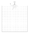
- FIG. 1 a wiring diagram of a transparent electronic display board having four-electrode light emitting elements is illustrated in FIG. 1 .
- FIG. 1 is a wiring diagram showing a conventional transparent electronic display board.
- the conventional transparent electronic display board includes: a plurality of light emitting elements 1 that is adhered between transparent plates facing each other by transparent resin; transparent electrodes 2 a through 2 d that are applied to either of transparent plates and are respectively connected to electrodes of the light emitting element to supply power to the light emitting element; and conductive tape 2 a ′ through 2 d ′ supplying power to the transparent electrodes 2 a through 2 d.
- Each light emitting element 1 comprises a four-electrode light emitting element 1 .
- the light emitting element 1 includes a single cathode electrode and three anode electrodes that are respectively connected to the transparent electrodes 2 a through 2 d extending from the transparent conductive tapes 2 a ′ through 2 d ′.
- the light emitting elements 1 are aligned in rows with respect to the vertical direction.
- a plurality of rows of light emitting elements 1 in each of which the light emitting elements 1 are aligned with each other in the vertical direction, are provided.
- the transparent electrodes 2 a through 2 d extend from opposite ends of the transparent plate and are respectively connected to the anode electrodes and the cathode electrode of the corresponding four-electrode light emitting element 1 .
- the transparent electrodes 2 a through 2 d are separated and insulated from each other such that they do not make contact with each other.
- the transparent electrodes 2 a through 2 d are configured such that they successively extended from the opposite ends of the transparent plate to the light emitting elements 1 aligned with each other on the central portion of the transparent plate. That is, the first transparent electrode 2 a , which is connected to the cathode electrode to function as a ground terminal, and the second through fourth transparent electrodes 2 b through 2 d , which are connected to the respective anode electrodes, are successively provided.
- the fifth through seventh transparent electrodes 2 e through 2 g connected to the corresponding anode electrodes are successively provided next to the fourth transparent electrodes 2 d .
- Another first transparent electrode connected to the cathode electrodes of other light emitting elements is provided next to the seventh transparent electrode. That is, in the conventional technique, the sixth through eighth transparent electrodes 2 f through 2 h connected to the anode electrodes are formed.
- the number of transparent electrodes that are connected to the cathode electrodes of the light emitting elements and function as ground terminals must be changed depending on the number of light emitting elements arranged in the vertical or horizontal direction. Therefore, the number of manufacturing processes becomes comparatively large, whereby production costs are increased, and productivity is reduced.
- an object of the present invention is to provide a transparent electronic display board configured such that a transparent electrode for cathode electrodes is connected as a common electrode to cathode electrodes of four-electrode light emitting elements. This reduces the number of processes for connecting the transparent electrode to the light emitting elements, whereby manufacturing times can be reduced, and productivity can be enhanced.
- a transparent electrode for cathode electrodes is connected in common to cathode electrodes of a plurality of light emitting elements.
- a design for wiring transparent electrodes connected to the light emitting element can be simplified. Therefore, the number of processes can be reduced, and productivity can be enhanced.
- FIG. 1 is a view showing a conventional transparent electronic display board.
- FIG. 2 is a view illustrating a transparent electronic display board according to the present invention.
- FIG. 3 is a view showing the wiring of transparent electrodes in the transparent electronic display board according to the present invention.
- FIG. 4 is an enlarged view of FIG. 3 .
- FIG. 5 is a flowchart showing a method of manufacturing the transparent electronic display board according to the present invention.
- FIG. 6 is a view showing another embodiment of the transparent electronic display board according to the present invention.
- FIG. 7 is an enlarged view of portion ‘B’ of FIG. 6 .
- a transparent electronic display board includes: a pair of transparent plates spaced apart from each other and bonded to each other by transparent resin charged into a space between the transparent plates; one or more light emitting elements fastened to any one selected from between the transparent plates; transparent electrodes formed on the selected transparent plate, the transparent electrodes being electrically connected to anode electrodes and cathode electrodes of the light emitting elements; and transparent conductive tape adhered to each of the transparent electrodes on one edge of the transparent plate, the transparent conductive tape supplying power to the corresponding transparent electrode.
- Each of the light emitting elements includes one or more anode electrodes.
- the transparent electrodes comprise one or more anode connection electrodes respectively connected to the anode electrodes, and a cathode connection electrode connected in common to the cathode electrodes formed on the respective light emitting elements.
- the cathode connection electrode and the anode connection electrodes may respectively include connection terminals successively extending from on at least one of an upper, lower, left and right edges of the transparent plates, the connection terminals being connected to the corresponding transparent conductive tape.
- the connection terminal of the cathode connection electrode may be disposed at an uppermost position.
- the connection terminals of the anode connection electrodes may be successively disposed below the connection terminal of the cathode connection electrode.
- the cathode connection electrode and the anode connection electrodes may respectively include connection terminals successively extending from on at least one of an upper, lower, left and right edges of the transparent plates, the connection terminals being connected to the corresponding transparent conductive tape.
- the connection terminal of the cathode connection electrode may be disposed at a lowermost position.
- the connection terminals of the anode connection electrodes may be successively disposed below the connection terminal of the cathode connection electrode.
- the anode connection electrodes may be respectively connected to the anode electrodes of each of the light emitting elements. At least one of the anode connection electrodes may be spaced apart from another of the anode connection electrodes by the cathode connection electrode disposed therebetween.
- the light emitting elements may form a plurality of light emitting element groups each including one or more light emitting elements arranged in a horizontal direction.
- the light emitting element groups may be successively arranged in a vertical direction.
- the number of anode connection electrodes may be equal to the number of anode electrodes of each of the light emitting elements.
- each of the anode connection electrodes may include extensions extending in one direction from at least one among an upper portion, a lower portion and a central portion of each of the light emitting element groups including the light emitting elements arranged in one direction, the extensions being connected to the corresponding anode electrodes of the respective light emitting elements.
- a seventh embodiment of the present invention is a method of manufacturing a transparent electronic display board, including: a transparent electrode forming operation of forming a transparent electrode on an entire area of the transparent plate; an anode-connection-electrode area partitioning operation of separating, from the transparent electrode, areas corresponding to anode connection electrodes connected to anode electrodes of light emitting elements after the transparent electrode forming operation; a transparent-conductive-tape adhesion operation of adhering transparent conductive tape to areas corresponding to the anode connection electrodes after the area partitioning operation; and a light-emitting-element adhesion operation of disposing the light emitting element such that the anode electrodes are aligned with the respective anode connection electrodes and then adhering the light emitting element to the transparent plate
- the anode-connection-electrode area partitioning operation may include forming the one or more anode connection electrodes corresponding to the number of anode electrodes of each of the light emitting elements.
- the anode connection electrodes may be disposed at one or more positions among above, below, and on a central portion of the areas on which the light emitting elements are adhered, such that the anode connection electrodes are spaced apart from each other in a vertical direction.
- the anode connection electrodes may extend in a direction in which the light emitting elements are arranged.
- the anode-connection-electrode area partitioning operation may include forming extensions extending from each of the anode connection electrodes toward the areas on which the light emitting elements are adhered.
- the extensions may be connected to the corresponding anode electrodes of the respective light emitting elements.
- FIG. 2 is a view illustrating a transparent electronic display board according to the present invention.
- FIG. 3 is a view showing the wiring of transparent electrodes in the transparent electronic display board according to the present invention.
- FIG. 4 is an enlarged view of a portion of FIG. 3 .
- the transparent electronic display board includes: a pair of transparent plates 10 that are spaced apart from each other by a predetermined distance and are adhered to each other by transparent resin; transparent electrodes 21 through 24 that are made of conductive material and are formed on either of the transparent plates 10 so as to introduce power; a plurality of light emitting elements 20 , 20 ′, 20 ′′, and 20 ′′′ that are fastened to either of the transparent plates 10 and emit light using power applied from the transparent electrodes 21 through 24 ; a controller 30 for controlling on or off states of the light emitting elements 20 ; and transparent conductive tape 25 supplying power to the transparent electrodes 21 through 24 .
- each transparent plate 10 Facing each other, the two transparent plates 10 are adhered to each other with transparent resin charged into a space between the transparent plates 10 .
- Each transparent plate 10 is made of any one of a transparent glass plate, acrylic glass, and polycarbonate.
- the combination between the transparent plate 10 and the light emitting elements 20 is a well-known technique; therefore, further explanation and illustration thereof will be omitted.
- Each light emitting element 20 is a luminous body turning light on or off depending on the supply of power.
- the light emitting elements 20 are fastened by conductive resin (not shown) to the transparent electrodes 21 , 22 , and 23 provided on a surface of either of the two transparent plates 10 .
- a lower end of each light emitting element 20 is fastened to the transparent electrodes 21 , 22 , and 23 .
- An upper portion of the light emitting element 20 is protected by the transparent resin and is adhered to the other transparent plate.
- Each light emitting element 20 has anode electrodes 20 a through 20 c and a cathode electrode 20 d . Positive power is input into or output from the anode electrodes 20 a , 20 b , and 20 c .
- Each light emitting element 20 may comprise any one of a two-electrode light emitting element having one anode electrode and one cathode electrode, a three-electrode light emitting element having two anode electrodes and one cathode electrode, and a four-electrode light emitting element 20 having three anode electrodes and one cathode electrode.
- a four-electrode light emitting element will be illustrated as one example.
- the transparent electrodes 21 through 24 are formed by applying any one of an Indium Tin Oxide (ITO), Indium Zinc Oxide (IZO), and liquid polymer, which are conductive materials, to a surface of a transparent plate that faces another transparent plate.
- the transparent electrodes 21 through 24 are partitioned and separated from each other such that they are insulated from each other and are respectively connected to the anode electrodes 20 a , 20 b , and 20 c and the cathode electrode 20 d of the light emitting element 20 .
- the anode connection electrodes 21 through 23 of the transparent electrodes 21 through 24 extend from one side of the transparent plate 10 of the entire area of the anode connection electrodes 21 through 23 in consideration of the positions of the anode electrodes of the light emitting elements, and are partitioned and separated from each other to form areas that respectively connect to the anode electrodes 20 a , 20 b , and 20 c.
- the partitioned transparent electrodes 21 through 24 are respectively connected to the anode electrodes 20 a , 20 b , and 20 c and the cathode electrode 20 d of the light emitting element 20 .
- the transparent electrodes 21 through 24 function to transmit control signals from the controller 30 to the light emitting element 20 .
- areas partitioned to be connected to the anode electrodes 20 a , 20 b , and 20 c of the light emitting element are respectively called the anode connection electrodes 21 through 23
- an area partitioned to be connected to the cathode electrode 20 d is called the cathode connection electrode 24 .
- the transparent electrodes 21 , 22 , 23 , and 24 comprise a plurality of groups of transparent electrodes 21 , 22 , 23 , and 24 .
- Each group of transparent electrodes 21 , 22 , 23 , 24 includes: one or more anode connection electrodes 21 through 23 that are respectively connected to the one or more anode electrodes 20 a , 20 b , and 20 c formed on the single light emitting element 20 ; and a cathode connection electrode 24 connected to the cathode electrode 20 d.
- the number of anode connection electrodes 21 through 23 corresponds to the number of the anode electrodes 20 a , 20 b , and 20 c of each light emitting element 20 ; however, the single cathode connection electrode 24 is connected in common to the cathode electrodes 20 d of a plurality of light emitting elements 20 .
- the transparent electrodes 21 through 24 comprise a plurality of groups each of which includes a first through third anode connection electrodes 21 through 23 that are respectively connected to a first through third anode electrodes 20 a , 20 b , and 20 c.
- a first group of anode connection electrodes 21 through 23 includes: a first anode connection electrode 21 connected to the first anode electrode 20 a of the first light emitting element 20 ; a second anode connection electrode 22 connected to the second anode electrode 20 b ; and a third anode connection electrode 23 connected to the third anode electrode 20 c.
- a second group of anode connection electrodes 21 ′, 22 ′, and 23 ′ includes first anode connection electrodes 21 ′ through 23 ′ that are respectively connected to the first through third anode electrodes 20 a , 20 b , and 20 c of the second light emitting element 20 . That is, the anode connection electrodes 21 through 23 of the transparent electrodes that form the plurality of groups are respectively connected to the one or more anode electrodes 20 a , 20 b , and 20 c formed on each light emitting element 20 .
- the cathode connection electrode 24 is used in common. In other words, it is connected in common to the cathode electrodes 20 d that are formed on the respective light emitting elements 20 .
- the present invention is characterized in that the single cathode connection electrode 24 is connected in common to the cathode electrodes 20 d of the light emitting elements 20 provided on the transparent electronic display board, and the anode connection electrodes 21 through 23 are respectively connected to the anode electrodes 20 a , 20 b , and 20 c of each light emitting element 20 .
- the anode connection electrodes 21 through 23 form connection terminals (not designated by reference numerals) that are provided on one edge of the transparent plate 10 and are successively arranged downward from an upper end of the edge.
- the connection terminals comprise start points from which the anode connection electrodes 21 through 23 extend, and to which the transparent conductive tape 25 is adhered.
- connection terminals of the anode connection electrodes 21 through 23 of the first group, connection terminals of the anode connection electrodes 21 ′ through 23 ′ of the second group, and the connection terminals of the anode connection electrodes 21 ′′ through 23 ′′ of the third group are successively formed from the upper end or one end of the edge of the transparent plate 10 .
- the transparent conductive tape 25 is adhered to each of the connection terminals that are the start points of the anode connection electrodes 21 through 23 .
- the anode connection electrodes 21 through 23 are respectively connected to the anode electrodes 20 a , 20 b , and 20 c of the light emitting elements 20 .
- the cathode connection electrode 24 corresponds to the entire area other than areas on which the anode connection electrodes 21 through 23 are formed.
- the transparent electrodes 21 through 24 are formed on the entirety of the transparent plate 10 . Thereafter, areas to which the anode connection electrodes 21 through 23 and the light emitting element 20 will be adhered are separated from each other such that they can be insulated from each other.
- the transparent conductive tape 25 is adhered to each of the areas allocated to the anode connection electrodes 21 through 23 so that electric signals can be transmitted between the controller 30 and the anode connection electrodes 21 through 23 .
- the present invention can be modified in a variety of ways as well as the above-mentioned embodiment.
- another embodiment of the present invention will be described in detail with reference to FIGS. 5 through 7 .
- FIG. 5 is a flowchart showing a method of manufacturing the transparent electronic display board according to the present invention.
- FIG. 6 is a view showing another embodiment of the transparent electronic display board according to the present invention.
- FIG. 7 is an enlarged view of portion ‘B’ of FIG. 6 .
- a light emitting element illustrated in FIGS. 5 through 7 comprises a four-electrode light emitting element including three anode electrodes and a single cathode electrode. The present invention is not limited to this. A two- or three-electrode light emitting element also falls within the technical bounds of the present invention.
- the transparent electronic display board includes: one or more light emitting element groups 201 , 202 , and 203 , each of which includes one or more light emitting element 20 , 20 ′, and 20 ′′ arranged in the horizontal direction; at least one cathode electrode 20 d connected in common to anode electrodes 20 a , 20 b , and 20 c of the light emitting elements 20 , 20 ′, and 20 ′′ of each light emitting element group 201 , 202 , 203 ; and a cathode connection electrode 24 connected in common to the cathode electrodes 20 d of the light emitting elements 20 , 20 ′, and 20 ′′.
- each light emitting element 20 , 20 ′, 20 ′′ includes one or more anode electrodes 20 a , 20 b , and 20 c and a single cathode electrode 20 d .
- One or more light emitting elements are arranged in the horizontal direction to form a single light emitting element group.
- the light emitting element groups 201 , 202 , and 203 are successively arranged from the upper end of the transparent plate 10 to the lower end thereof.
- Each light emitting element group 201 , 202 , 203 includes one or more light emitting elements 20 , 20 ′, and 20 ′′ that are arranged in the horizontal direction at positions spaced apart from each other.
- Each light emitting element 20 , 20 ′, 20 ′′ may comprise any one of two-, three-, and four-electrode light emitting elements. In this embodiment, a four-electrode light emitting element will be illustrated as one example.
- the anode connection electrodes 21 , 22 , and 23 comprise at least one group of anode connection electrodes.
- the anode connection electrodes 21 , 22 , and 23 of each group extend from one side of the transparent plate 10 and are connected to the anode electrodes 20 a , 20 b , and 20 c of the light emitting elements 20 , 20 ′, and 20 ′′ of the corresponding light emitting element group.
- the number of anode connection electrodes 21 , 22 , and 23 is the same as that of the anode electrodes 20 a , 20 b , and 20 c of each light emitting element 20 , 20 ′, 20 ′′.
- Each anode connection electrode 21 , 22 , 23 is connected in common to the corresponding anode electrodes 20 a , 20 b , 20 c of the light emitting elements of the same light emitting element group.
- a first group of anode connection electrodes 21 , 22 , and 23 that is connected to the first light emitting element group includes: a first anode connection electrode 21 that is connected to the first anode electrodes 20 a of the light emitting elements of the first light emitting element group 201 ; a second anode connection electrode 22 that is connected in common to the second anode electrodes 20 b of the first light emitting element group 201 ; and a third anode connection electrode 23 that is connected to the third anode electrodes 20 c of the first light emitting element group 201 .
- the cathode connection electrode 24 is connected in common to the cathode electrodes of all of the light emitting elements 20 , 20 ′, and 20 ′′ of the first light emitting element group 201 and thus functions as a ground terminal.
- the first anode connection electrode 21 is disposed at an upper position of each light emitting element group 201 , 202 , 203 and extends in the direction in which the light emitting elements 20 , 20 ′, 20 ′′, and 20 ′′′ are arranged.
- the third anode connection electrode 23 is disposed at a lower position of each light emitting element group 201 , 202 , 203 and extends in the direction in which the light emitting elements 20 , 20 ′, 20 ′′, and 20 ′′′ are arranged.
- the second anode connection electrode 22 is disposed between the first anode connection electrode 21 and the third anode connection electrode 23 and extends in the direction of the arrangement of the light emitting element group.
- the first anode connection electrode 21 and the third anode connection electrode 23 extend in one direction with a group (for example, 201 of FIG. 6 ) of light emitting elements 20 , 20 ′, 20 ′′, and 20 ′′′ disposed between the first and third anode connection electrodes 21 and 23 .
- the first anode connection electrode 21 and the third anode connection electrode 23 respectively include a plurality of extensions 211 and a plurality of extensions 231 that are extended toward and connected to the first and third anode electrodes 20 a and 20 c of the light emitting elements 20 , 20 ′, 20 ′′, and 20 ′′′ of the first light emitting element group 201 .
- the first anode connection electrode 21 extends in the horizontal direction and includes one or more first extensions 211 that are respectively connected to the first anode electrodes 20 a of the light emitting elements 20 , 20 ′, 20 ′′, and 20 ′′′, which are disposed below the first anode connection electrode 21 .
- the third anode connection electrode 23 includes one or more second extensions 231 that are respectively connected to the third anode electrodes 20 c of the light emitting elements.
- the second anode connection electrode 22 extends from one side of the transparent plate 10 towards the other side and passes through a central portion of an area in which the light emitting element group is disposed.
- the second anode connection electrode 22 is connected in common to the second anode electrodes 20 b of the light emitting elements that belong to each light emitting element group 201 , 202 , 203 .
- the first through third anode connection electrodes 21 through 23 are configured such that they are partitioned and insulated from the transparent electrode (cathode connection electrode) 24 applied to the entirety of the transparent plate 10 and have portions that extend depending on the positions of the light emitting elements 20 , 20 ′, 20 ′′, and 20 ′′′. Therefore, it is unnecessary to form a separate cathode connection electrode.
- the method of manufacturing the transparent electronic display board according to the present invention includes: a transparent electrode forming operation S 10 of forming a transparent electrode on an entire area of the transparent plate 10 ; an anode-connection-electrode area partitioning operation S 20 of separating, from the transparent electrode, areas corresponding to the anode connection electrodes 21 , 22 , and 23 that are connected to the anode electrodes 20 a , 20 b , and 20 c of the light emitting elements 20 after the transparent electrode forming operation S 10 ; a transparent-conductive-tape adhesion operation S 30 of adhering the transparent conductive tape 25 to the anode connection electrodes 21 , 22 , and 23 after the area partitioning operation S 20 ; a light-emitting-element adhesion operation S 40 of disposing the light emitting element 20 such that the anode electrodes 20 a , 20 b , and 20 c correspond to the respective anode connection electrodes 21 , 22 , and 23 and then adhering the light emitting
- the transparent electrode is formed on the entire area of either of the two transparent plates 10 forming the transparent electronic display board.
- each anode connection electrode 21 , 22 , 23 has a connection terminal on one edge of the transparent plate 10 and is formed by an area extending from the connection terminal to the area for bonding the light emitting element 20 .
- the anode connection electrodes 21 , 22 , and 23 are formed such that they are insulated from adjacent anode connection electrodes 21 ′, 22 ′, and 23 ′.
- connection terminals are successively formed on one edge of the transparent plate 10 .
- the connection terminals of the anode connection electrodes 21 , 22 , and 23 are successively formed according to the order in which the light emitting elements 20 are positioned.
- a connection terminal of the transparent electrode (cathode connection electrode) 24 that is first formed is disposed at the uppermost or lowermost end of the edge of the transparent plate 10 .
- the transparent electrode that is first formed is partitioned into the anode connection electrodes 21 , 22 , and 23 .
- the area of the transparent electrode other than the anode connection electrodes 21 , 22 , and 23 forms the cathode connection electrode 24 that is connected to the cathode electrodes 20 d of the light emitting elements 20 . Therefore, in the present invention, only the anode connection electrodes 21 , 22 , and 23 are separately formed unlike the conventional technique in which the anode connection electrodes 21 , 22 , and 23 , and the cathode connection electrode must be individually formed through separate processes. Therefore, the present invention can markedly reduce the number of processes and the manufacturing times compared to conventional techniques.
- the transparent conductive tape 25 is adhered to start ends of the anode connection electrodes 21 , 22 , and 23 .
- the transparent conductive tape 25 is electrically connected to the controller 30 and functions to transmit a control signal for the light emitting elements 20 from the controller 30 to the anode connection electrodes.
- the ends of the anode connection electrodes 21 , 22 , and 23 are respectively aligned with the anode electrodes 20 a , 20 b , and 20 c . Thereafter, the light emitting element 20 is adhered to the transparent plate by transparent resin or conductive transparent resin.
- the resin filling and hardening operation S 50 after the light-emitting-element adhesion operation S 40 , the other transparent plate 10 comes into contact with the transparent plate 10 on which the transparent electrode is formed. Subsequently, transparent resin is charged into the space between the transparent plates 10 so that the transparent plates 10 are adhered to each other. The transparent resin is thereafter hardened at room temperature, thus completing the transparent electronic display board.
- the transparent electronic display board manufactured through the above-mentioned process does not require a separate transparent electrode connected to the cathode electrode 20 d of each light emitting element 20 . Therefore, the manufacturing process can be simplified compared to that of conventional techniques.
- the above-mentioned manufacturing method pertains to the transparent electronic display board according to the preceding embodiment.
- a method of manufacturing the transparent electronic display board according to another embodiment will be explained. Detailed explanation of the same operations as that of the manufacturing method pertaining to the preceding embodiment will be omitted.
- first through third anode connection electrodes 21 through 23 extend from one edge of the transparent plate 10 in the direction in which the elements of each light emitting element group are arranged.
- the first anode connection electrode 21 and the third anode connection electrode 23 are disposed at the upper and lower positions spaced apart from each other by a predetermined distance.
- the second anode connection electrode 22 is disposed between the first anode connection electrode 21 and the third anode connection electrode 23 .
- the third anode connection electrode 23 includes second extensions 231 vertically extending from the respective areas, on which the light emitting elements 20 , 20 ′, 20 ′′, and 20 ′′′ are placed, to positions corresponding to the third anode electrodes 20 c of the light emitting elements 20 , 20 ′, 20 ′′, and 20 ′′′.
- the second anode connection electrode 22 is disposed between the first extension 211 and the second extension 231 and extends from one side of the transparent plate 10 toward the other side thereof.
- the first anode connection electrode 21 , the second anode connection electrode 22 and the third anode connection electrode 23 are disposed such that the anode electrodes 20 a , 20 b , and 20 c of each of the light emitting elements 20 , 20 ′, 20 ′′, and 20 ′′′ are connected to the first through third anode connection electrodes 21 through 23 .
- the first through third anode connection electrodes 21 through 23 are thereafter adhered to the transparent plate.
- the first anode electrode 20 a of the light emitting element 20 is connected to the first extension 211 extending from the first anode connection electrode 21 .
- the second anode electrode 20 b is connected to the second anode connection electrode 22 .
- the third anode electrode 20 c is connected to the second extension 231 from the third anode connection electrode 23 .
- the cathode electrodes 20 d of the light emitting elements 20 , 20 ′, 20 ′′, and 20 ′′′ are brought into contact with areas of the first-formed transparent electrode 24 other than the first through third anode connection electrodes 21 through 23 . Therefore, it is unnecessary to form a separate cathode connection electrode.
- a transparent electrode is formed such that it is connected in common to cathode electrodes of a plurality of light emitting elements. Therefore, wiring for the transparent electrode connected to the light emitting elements can be easily designed. Furthermore, the number of processes can be reduced, and productivity can be enhanced.
Applications Claiming Priority (3)
| Application Number | Priority Date | Filing Date | Title |
|---|---|---|---|
| KR1020120078116A KR101188747B1 (ko) | 2012-07-18 | 2012-07-18 | 투명전광판 및 그 제조방법 |
| KR10-2012-0078116 | 2012-07-18 | ||
| PCT/KR2012/010103 WO2014014169A1 (ko) | 2012-07-18 | 2012-11-27 | 투명전광판 및 그 제조방법 |
Publications (2)
| Publication Number | Publication Date |
|---|---|
| US20150235578A1 US20150235578A1 (en) | 2015-08-20 |
| US10170023B2 true US10170023B2 (en) | 2019-01-01 |
Family
ID=47287572
Family Applications (1)
| Application Number | Title | Priority Date | Filing Date |
|---|---|---|---|
| US14/415,723 Active US10170023B2 (en) | 2012-07-18 | 2012-11-27 | Transparent electronic display board and method for manufacturing same |
Country Status (11)
| Country | Link |
|---|---|
| US (1) | US10170023B2 (ko) |
| EP (1) | EP2879120A4 (ko) |
| JP (1) | JP6153608B2 (ko) |
| KR (1) | KR101188747B1 (ko) |
| CN (1) | CN103827947B (ko) |
| BR (1) | BR112015000738A2 (ko) |
| HK (1) | HK1196457A1 (ko) |
| MX (1) | MX338760B (ko) |
| RU (1) | RU2595982C1 (ko) |
| SG (1) | SG11201500327PA (ko) |
| WO (1) | WO2014014169A1 (ko) |
Families Citing this family (27)
| Publication number | Priority date | Publication date | Assignee | Title |
|---|---|---|---|---|
| KR101442705B1 (ko) * | 2012-10-18 | 2014-09-19 | 지스마트 주식회사 | 균일한 광출력이 가능한 투명전광판 |
| KR101434954B1 (ko) * | 2013-02-15 | 2014-08-28 | 지스마트 주식회사 | 투명전광판을 구비한 무빙워크 |
| KR101434953B1 (ko) * | 2013-02-15 | 2014-08-28 | 지스마트 주식회사 | 투명전광판을 구비한 탑승교 |
| KR101434955B1 (ko) | 2013-03-18 | 2014-08-29 | 지스마트 주식회사 | 투명전광판의 접착제 도포방법 |
| KR101459310B1 (ko) * | 2013-12-10 | 2014-11-10 | 지스마트 주식회사 | 투명전광판의 고정장치 |
| KR101512661B1 (ko) * | 2013-12-10 | 2015-04-17 | 지스마트 주식회사 | 창틀에 설치가능한 복층 구조를 갖는 투명전광판 및 그 제조방법 |
| KR20160049613A (ko) * | 2014-10-27 | 2016-05-10 | 지스마트 주식회사 | 처짐 방지수단을 구비한 투명전광판의 제조방법 |
| KR101649212B1 (ko) * | 2014-10-27 | 2016-08-19 | 지스마트 주식회사 | 재귀반사방지수단을 구비한 투명전광판 |
| CN104715680B (zh) * | 2014-11-07 | 2017-08-11 | G思玛特有限公司 | 可绝缘的透明电子显示屏 |
| KR101784406B1 (ko) * | 2015-02-25 | 2017-10-12 | 금호전기주식회사 | 투명 전광 장치 |
| CN104715684A (zh) * | 2015-03-30 | 2015-06-17 | 赵琪科 | 透光玻璃显示屏及制造方法 |
| KR101581745B1 (ko) | 2015-04-12 | 2015-12-31 | 이동원 | 칩 led 및 그를 이용한 투명전광판 |
| KR101689131B1 (ko) * | 2015-07-24 | 2016-12-23 | 케이알에코스타 주식회사 | 메탈 메쉬를 이용한 투명 디스플레이 |
| KR101584739B1 (ko) | 2015-08-26 | 2016-01-13 | 주식회사 누리플랜 | 투명전광판 및 그 제조방법 |
| KR101584734B1 (ko) | 2015-09-08 | 2016-01-13 | 주식회사 누리플랜 | 투명전광판 및 그 제조방법 |
| KR101763107B1 (ko) | 2015-09-14 | 2017-08-07 | 루미마이크로 주식회사 | 발광 패키지 및 이를 포함하는 투명 디스플레이 장치 |
| KR101780688B1 (ko) | 2015-09-14 | 2017-10-23 | 루미마이크로 주식회사 | 네트패턴을 갖는 메쉬형 전극배선 및 이를 포함하는 led 투명전광판 |
| KR101785528B1 (ko) | 2015-09-14 | 2017-10-17 | 루미마이크로 주식회사 | 네트패턴을 갖는 led 투명전광판 배선구조 |
| KR101618861B1 (ko) | 2015-10-28 | 2016-05-11 | 주식회사 누리플랜 | 투명전광판 고정장치 |
| KR101842680B1 (ko) * | 2017-02-07 | 2018-03-27 | 주식회사 누리플랜 | 방음벽 구조물 |
| KR102275576B1 (ko) | 2017-08-08 | 2021-07-12 | 엘지전자 주식회사 | 디스플레이 디바이스 |
| KR102577090B1 (ko) | 2018-01-26 | 2023-09-12 | 엘지전자 주식회사 | 반도체 발광 소자를 이용한 램프 |
| DE102018107309B4 (de) | 2018-03-27 | 2019-10-10 | Symonics GmbH | Transparente Anzeigevorrichtung |
| TWI720418B (zh) * | 2019-01-31 | 2021-03-01 | 致伸科技股份有限公司 | 半導體發光單元及其封裝方法 |
| CN110137165B (zh) * | 2019-04-19 | 2021-10-12 | 开发晶照明(厦门)有限公司 | 显示器件及其制作方法 |
| KR20210099461A (ko) | 2020-02-04 | 2021-08-12 | 주식회사 국영지앤엠 | 투명 엘이디 디스플레이 패널 및 이의 제조 방법 |
| KR102639991B1 (ko) | 2022-05-26 | 2024-03-19 | 주식회사 루미디아 | 방수 및 방진 구조를 갖는 투명 led 디스플레이 모듈 및 이의 제조방법 |
Citations (11)
| Publication number | Priority date | Publication date | Assignee | Title |
|---|---|---|---|---|
| US5691738A (en) * | 1994-03-30 | 1997-11-25 | Nippondenso Co., Ltd. | Thin-film electroluminescent display and method of fabricating same |
| KR20020016493A (ko) | 2000-08-25 | 2002-03-04 | 후쿠시마 쓰토무 | 표시창용 투명패널의 제조방법 |
| US20050053801A1 (en) * | 2003-08-05 | 2005-03-10 | Andreas Elschner | Transparent electrode for electro-optical structures |
| KR20060007270A (ko) | 2004-07-19 | 2006-01-24 | 주식회사 미라클 | 투명표시창 및 그 제조방법 |
| US20080225523A1 (en) * | 2005-03-30 | 2008-09-18 | Koninklijke Philips Electronics N.V. | Flexible Led Array |
| US7498733B2 (en) * | 2004-09-29 | 2009-03-03 | Casio Computer Co., Ltd. | Display panel |
| US20110186846A1 (en) * | 2010-02-03 | 2011-08-04 | Samsung Mobile Display Co., Ltd. | Organic Light Emitting Display Device |
| US20110199554A1 (en) * | 2010-02-15 | 2011-08-18 | Hitachi Displays, Ltd. | Liquid crystal display device |
| US8058653B2 (en) * | 2008-02-20 | 2011-11-15 | Samsung Electronics Co., Ltd. | Thin film transistor array panel |
| KR20120009118A (ko) | 2010-07-22 | 2012-02-01 | 현대모비스 주식회사 | 차량용 투명 전광판 |
| US8426846B2 (en) * | 2006-03-30 | 2013-04-23 | Konica Minolta Holdings, Inc. | Organic electroluminescent element, method of manufacturing organic electroluminescent element, lighting device, and display device |
Family Cites Families (13)
| Publication number | Priority date | Publication date | Assignee | Title |
|---|---|---|---|---|
| SU1037326A1 (ru) * | 1982-02-08 | 1983-08-23 | Ордена Ленина Физический Институт Им.П.Н.Лебедева | Оптоэлектронный дисплей |
| JPH07282604A (ja) * | 1994-04-12 | 1995-10-27 | Sanyo Electric Works Ltd | 発光表示体及び同発光表示体を用いた発光表示装置 |
| ATE546836T1 (de) * | 2005-04-21 | 2012-03-15 | Fiat Ricerche | Anwendung einer transparenten leuchtdiodenanzeigevorrichtung in einem kraftfahrzeug |
| KR100618942B1 (ko) * | 2005-11-08 | 2006-09-01 | 김성규 | 투명전광판 |
| KR100618941B1 (ko) * | 2005-11-08 | 2006-09-01 | 김성규 | 투명발광장치 및 그 제조방법 |
| KR100618943B1 (ko) * | 2005-12-13 | 2006-09-01 | 김성규 | 투명전광판 및 이에 사용되는 칩 엘이디 |
| KR20080060490A (ko) * | 2006-12-27 | 2008-07-02 | 김성규 | 투명전광판 |
| KR20080098245A (ko) * | 2007-05-04 | 2008-11-07 | 김성규 | 투명발광장치 |
| JP2009157015A (ja) * | 2007-12-26 | 2009-07-16 | Komaden:Kk | Led表示装置及びled表示ユニット |
| JP5070190B2 (ja) * | 2008-12-03 | 2012-11-07 | シチズンホールディングス株式会社 | 液晶光学素子及び光ピックアップ装置 |
| DE202008017988U1 (de) * | 2008-05-26 | 2011-02-10 | C.R.F. Società Consortile per Azioni, Orbassano | Transparente Anzeigevorrichtung mit Leiterbahnen, die mit undurchsichtiger Beschichtung versehen sind |
| CN101447507A (zh) * | 2008-12-12 | 2009-06-03 | 信利半导体有限公司 | 一种具有触摸屏功能的有机电致发光显示器 |
| CN202003646U (zh) * | 2011-03-07 | 2011-10-05 | 安徽众和达光电有限公司 | 一种led数码显示屏 |
-
2012
- 2012-07-18 KR KR1020120078116A patent/KR101188747B1/ko active IP Right Grant
- 2012-11-27 EP EP12881275.7A patent/EP2879120A4/en not_active Ceased
- 2012-11-27 US US14/415,723 patent/US10170023B2/en active Active
- 2012-11-27 RU RU2015101101/12A patent/RU2595982C1/ru not_active IP Right Cessation
- 2012-11-27 MX MX2015000634A patent/MX338760B/es active IP Right Grant
- 2012-11-27 JP JP2015521524A patent/JP6153608B2/ja active Active
- 2012-11-27 CN CN201280036311.2A patent/CN103827947B/zh not_active Expired - Fee Related
- 2012-11-27 BR BR112015000738A patent/BR112015000738A2/pt not_active IP Right Cessation
- 2012-11-27 WO PCT/KR2012/010103 patent/WO2014014169A1/ko active Application Filing
- 2012-11-27 SG SG11201500327PA patent/SG11201500327PA/en unknown
-
2014
- 2014-09-27 HK HK14109751.4A patent/HK1196457A1/xx not_active IP Right Cessation
Patent Citations (11)
| Publication number | Priority date | Publication date | Assignee | Title |
|---|---|---|---|---|
| US5691738A (en) * | 1994-03-30 | 1997-11-25 | Nippondenso Co., Ltd. | Thin-film electroluminescent display and method of fabricating same |
| KR20020016493A (ko) | 2000-08-25 | 2002-03-04 | 후쿠시마 쓰토무 | 표시창용 투명패널의 제조방법 |
| US20050053801A1 (en) * | 2003-08-05 | 2005-03-10 | Andreas Elschner | Transparent electrode for electro-optical structures |
| KR20060007270A (ko) | 2004-07-19 | 2006-01-24 | 주식회사 미라클 | 투명표시창 및 그 제조방법 |
| US7498733B2 (en) * | 2004-09-29 | 2009-03-03 | Casio Computer Co., Ltd. | Display panel |
| US20080225523A1 (en) * | 2005-03-30 | 2008-09-18 | Koninklijke Philips Electronics N.V. | Flexible Led Array |
| US8426846B2 (en) * | 2006-03-30 | 2013-04-23 | Konica Minolta Holdings, Inc. | Organic electroluminescent element, method of manufacturing organic electroluminescent element, lighting device, and display device |
| US8058653B2 (en) * | 2008-02-20 | 2011-11-15 | Samsung Electronics Co., Ltd. | Thin film transistor array panel |
| US20110186846A1 (en) * | 2010-02-03 | 2011-08-04 | Samsung Mobile Display Co., Ltd. | Organic Light Emitting Display Device |
| US20110199554A1 (en) * | 2010-02-15 | 2011-08-18 | Hitachi Displays, Ltd. | Liquid crystal display device |
| KR20120009118A (ko) | 2010-07-22 | 2012-02-01 | 현대모비스 주식회사 | 차량용 투명 전광판 |
Non-Patent Citations (1)
| Title |
|---|
| International Search Report for PCT/KR2012/010103. |
Also Published As
| Publication number | Publication date |
|---|---|
| EP2879120A1 (en) | 2015-06-03 |
| MX338760B (es) | 2016-04-29 |
| CN103827947B (zh) | 2015-09-02 |
| CN103827947A (zh) | 2014-05-28 |
| EP2879120A4 (en) | 2016-02-17 |
| WO2014014169A1 (ko) | 2014-01-23 |
| MX2015000634A (es) | 2015-07-06 |
| SG11201500327PA (en) | 2015-03-30 |
| HK1196457A1 (en) | 2014-12-12 |
| US20150235578A1 (en) | 2015-08-20 |
| BR112015000738A2 (pt) | 2017-06-27 |
| RU2595982C1 (ru) | 2016-08-27 |
| JP2015523604A (ja) | 2015-08-13 |
| KR101188747B1 (ko) | 2012-10-10 |
| JP6153608B2 (ja) | 2017-06-28 |
Similar Documents
| Publication | Publication Date | Title |
|---|---|---|
| US10170023B2 (en) | Transparent electronic display board and method for manufacturing same | |
| US9752732B2 (en) | Transparent electronic display board and method for manufacturing same | |
| TWI386724B (zh) | 使用發光二極體之線性光源及使用該光源之鏡片及背光單元 | |
| WO2017005225A2 (zh) | Led发光组件、led发光面板和led显示屏 | |
| KR100618943B1 (ko) | 투명전광판 및 이에 사용되는 칩 엘이디 | |
| US9805629B2 (en) | Transparent electronic display board capable of uniform optical output | |
| KR20090079415A (ko) | 표시 장치용 광원 모듈 및 이를 포함하는 표시 장치 | |
| CN106094299B (zh) | 显示装置 | |
| JP2008505509A (ja) | 透明発光装置及びその製造方法 | |
| CN110972495A (zh) | 发光驱动基板及其制作方法、发光基板和显示装置 | |
| CN110658651B (zh) | 灯板、背光模组以及显示装置 | |
| CN102956627A (zh) | Led封装结构 | |
| CN102695364A (zh) | Oled光源用fpc、oled光源及oled光源引出电极的连接方法 | |
| KR102084718B1 (ko) | 백라이트 유닛 및 이를 포함하는 표시 장치 및 그 제조 방법 | |
| KR100794474B1 (ko) | 선을 이용한 투명패널 라이팅 | |
| CN205680679U (zh) | 一种侧贴片式全彩led封装 | |
| CN104050887A (zh) | 彩色透明电子显示板及其制造方法 | |
| CN113433735A (zh) | 背光模块、背光板、显示屏和电子设备 | |
| KR20150092924A (ko) | 발광 다이오드 어레이 및 디스플레이 장치 | |
| CN201819073U (zh) | 一种背光模组 | |
| CN104183585A (zh) | 一种芯片层叠结构及控制led的方法 | |
| CN103887388A (zh) | 一种透明柔性led显示芯片 | |
| KR101593415B1 (ko) | 표시 장치용 광원 모듈 및 이를 포함하는 표시 장치 | |
| CN106851915A (zh) | 一种智能显示建筑玻璃及其导电线路 | |
| CN107103846A (zh) | 能够扩大发光面积的透明导光板 |
Legal Events
| Date | Code | Title | Description |
|---|---|---|---|
| AS | Assignment |
Owner name: G-SMATT CO., LTD., KOREA, REPUBLIC OF Free format text: ASSIGNMENT OF ASSIGNORS INTEREST;ASSIGNOR:LEE, HO JUN;REEL/FRAME:034747/0968 Effective date: 20141218 |
|
| STCF | Information on status: patent grant |
Free format text: PATENTED CASE |
|
| MAFP | Maintenance fee payment |
Free format text: PAYMENT OF MAINTENANCE FEE, 4TH YR, SMALL ENTITY (ORIGINAL EVENT CODE: M2551); ENTITY STATUS OF PATENT OWNER: SMALL ENTITY Year of fee payment: 4 |