KR20130140782A - 집적 회로 장치에서 내부 전원을 공유하기 위한 방법 및 장치 - Google Patents
집적 회로 장치에서 내부 전원을 공유하기 위한 방법 및 장치 Download PDFInfo
- Publication number
- KR20130140782A KR20130140782A KR1020137015142A KR20137015142A KR20130140782A KR 20130140782 A KR20130140782 A KR 20130140782A KR 1020137015142 A KR1020137015142 A KR 1020137015142A KR 20137015142 A KR20137015142 A KR 20137015142A KR 20130140782 A KR20130140782 A KR 20130140782A
- Authority
- KR
- South Korea
- Prior art keywords
- supply voltage
- regulator
- voltage generator
- memory device
- internal
- Prior art date
Links
Images

Classifications
-
- G—PHYSICS
- G11—INFORMATION STORAGE
- G11C—STATIC STORES
- G11C5/00—Details of stores covered by group G11C11/00
- G11C5/14—Power supply arrangements, e.g. power down, chip selection or deselection, layout of wirings or power grids, or multiple supply levels
-
- G—PHYSICS
- G11—INFORMATION STORAGE
- G11C—STATIC STORES
- G11C5/00—Details of stores covered by group G11C11/00
- G11C5/14—Power supply arrangements, e.g. power down, chip selection or deselection, layout of wirings or power grids, or multiple supply levels
- G11C5/147—Voltage reference generators, voltage or current regulators; Internally lowered supply levels; Compensation for voltage drops
-
- G—PHYSICS
- G11—INFORMATION STORAGE
- G11C—STATIC STORES
- G11C11/00—Digital stores characterised by the use of particular electric or magnetic storage elements; Storage elements therefor
- G11C11/21—Digital stores characterised by the use of particular electric or magnetic storage elements; Storage elements therefor using electric elements
- G11C11/34—Digital stores characterised by the use of particular electric or magnetic storage elements; Storage elements therefor using electric elements using semiconductor devices
- G11C11/40—Digital stores characterised by the use of particular electric or magnetic storage elements; Storage elements therefor using electric elements using semiconductor devices using transistors
- G11C11/401—Digital stores characterised by the use of particular electric or magnetic storage elements; Storage elements therefor using electric elements using semiconductor devices using transistors forming cells needing refreshing or charge regeneration, i.e. dynamic cells
- G11C11/4063—Auxiliary circuits, e.g. for addressing, decoding, driving, writing, sensing or timing
- G11C11/407—Auxiliary circuits, e.g. for addressing, decoding, driving, writing, sensing or timing for memory cells of the field-effect type
- G11C11/4074—Power supply or voltage generation circuits, e.g. bias voltage generators, substrate voltage generators, back-up power, power control circuits
-
- G—PHYSICS
- G11—INFORMATION STORAGE
- G11C—STATIC STORES
- G11C16/00—Erasable programmable read-only memories
- G11C16/02—Erasable programmable read-only memories electrically programmable
- G11C16/06—Auxiliary circuits, e.g. for writing into memory
- G11C16/10—Programming or data input circuits
- G11C16/12—Programming voltage switching circuits
-
- G—PHYSICS
- G11—INFORMATION STORAGE
- G11C—STATIC STORES
- G11C16/00—Erasable programmable read-only memories
- G11C16/02—Erasable programmable read-only memories electrically programmable
- G11C16/06—Auxiliary circuits, e.g. for writing into memory
- G11C16/30—Power supply circuits
-
- G—PHYSICS
- G11—INFORMATION STORAGE
- G11C—STATIC STORES
- G11C5/00—Details of stores covered by group G11C11/00
- G11C5/14—Power supply arrangements, e.g. power down, chip selection or deselection, layout of wirings or power grids, or multiple supply levels
- G11C5/145—Applications of charge pumps; Boosted voltage circuits; Clamp circuits therefor
-
- H—ELECTRICITY
- H01—ELECTRIC ELEMENTS
- H01L—SEMICONDUCTOR DEVICES NOT COVERED BY CLASS H10
- H01L25/00—Assemblies consisting of a plurality of individual semiconductor or other solid state devices ; Multistep manufacturing processes thereof
- H01L25/03—Assemblies consisting of a plurality of individual semiconductor or other solid state devices ; Multistep manufacturing processes thereof all the devices being of a type provided for in the same subgroup of groups H01L27/00 - H01L33/00, or in a single subclass of H10K, H10N, e.g. assemblies of rectifier diodes
- H01L25/04—Assemblies consisting of a plurality of individual semiconductor or other solid state devices ; Multistep manufacturing processes thereof all the devices being of a type provided for in the same subgroup of groups H01L27/00 - H01L33/00, or in a single subclass of H10K, H10N, e.g. assemblies of rectifier diodes the devices not having separate containers
- H01L25/065—Assemblies consisting of a plurality of individual semiconductor or other solid state devices ; Multistep manufacturing processes thereof all the devices being of a type provided for in the same subgroup of groups H01L27/00 - H01L33/00, or in a single subclass of H10K, H10N, e.g. assemblies of rectifier diodes the devices not having separate containers the devices being of a type provided for in group H01L27/00
- H01L25/0657—Stacked arrangements of devices
-
- H—ELECTRICITY
- H01—ELECTRIC ELEMENTS
- H01L—SEMICONDUCTOR DEVICES NOT COVERED BY CLASS H10
- H01L2224/00—Indexing scheme for arrangements for connecting or disconnecting semiconductor or solid-state bodies and methods related thereto as covered by H01L24/00
- H01L2224/01—Means for bonding being attached to, or being formed on, the surface to be connected, e.g. chip-to-package, die-attach, "first-level" interconnects; Manufacturing methods related thereto
- H01L2224/02—Bonding areas; Manufacturing methods related thereto
- H01L2224/04—Structure, shape, material or disposition of the bonding areas prior to the connecting process
- H01L2224/0401—Bonding areas specifically adapted for bump connectors, e.g. under bump metallisation [UBM]
-
- H—ELECTRICITY
- H01—ELECTRIC ELEMENTS
- H01L—SEMICONDUCTOR DEVICES NOT COVERED BY CLASS H10
- H01L2224/00—Indexing scheme for arrangements for connecting or disconnecting semiconductor or solid-state bodies and methods related thereto as covered by H01L24/00
- H01L2224/01—Means for bonding being attached to, or being formed on, the surface to be connected, e.g. chip-to-package, die-attach, "first-level" interconnects; Manufacturing methods related thereto
- H01L2224/02—Bonding areas; Manufacturing methods related thereto
- H01L2224/04—Structure, shape, material or disposition of the bonding areas prior to the connecting process
- H01L2224/04042—Bonding areas specifically adapted for wire connectors, e.g. wirebond pads
-
- H—ELECTRICITY
- H01—ELECTRIC ELEMENTS
- H01L—SEMICONDUCTOR DEVICES NOT COVERED BY CLASS H10
- H01L2224/00—Indexing scheme for arrangements for connecting or disconnecting semiconductor or solid-state bodies and methods related thereto as covered by H01L24/00
- H01L2224/01—Means for bonding being attached to, or being formed on, the surface to be connected, e.g. chip-to-package, die-attach, "first-level" interconnects; Manufacturing methods related thereto
- H01L2224/10—Bump connectors; Manufacturing methods related thereto
- H01L2224/12—Structure, shape, material or disposition of the bump connectors prior to the connecting process
- H01L2224/13—Structure, shape, material or disposition of the bump connectors prior to the connecting process of an individual bump connector
- H01L2224/13001—Core members of the bump connector
- H01L2224/13005—Structure
- H01L2224/13009—Bump connector integrally formed with a via connection of the semiconductor or solid-state body
-
- H—ELECTRICITY
- H01—ELECTRIC ELEMENTS
- H01L—SEMICONDUCTOR DEVICES NOT COVERED BY CLASS H10
- H01L2225/00—Details relating to assemblies covered by the group H01L25/00 but not provided for in its subgroups
- H01L2225/03—All the devices being of a type provided for in the same subgroup of groups H01L27/00 - H01L33/648 and H10K99/00
- H01L2225/04—All the devices being of a type provided for in the same subgroup of groups H01L27/00 - H01L33/648 and H10K99/00 the devices not having separate containers
- H01L2225/065—All the devices being of a type provided for in the same subgroup of groups H01L27/00 - H01L33/648 and H10K99/00 the devices not having separate containers the devices being of a type provided for in group H01L27/00
- H01L2225/06503—Stacked arrangements of devices
- H01L2225/0651—Wire or wire-like electrical connections from device to substrate
-
- H—ELECTRICITY
- H01—ELECTRIC ELEMENTS
- H01L—SEMICONDUCTOR DEVICES NOT COVERED BY CLASS H10
- H01L2225/00—Details relating to assemblies covered by the group H01L25/00 but not provided for in its subgroups
- H01L2225/03—All the devices being of a type provided for in the same subgroup of groups H01L27/00 - H01L33/648 and H10K99/00
- H01L2225/04—All the devices being of a type provided for in the same subgroup of groups H01L27/00 - H01L33/648 and H10K99/00 the devices not having separate containers
- H01L2225/065—All the devices being of a type provided for in the same subgroup of groups H01L27/00 - H01L33/648 and H10K99/00 the devices not having separate containers the devices being of a type provided for in group H01L27/00
- H01L2225/06503—Stacked arrangements of devices
- H01L2225/06541—Conductive via connections through the device, e.g. vertical interconnects, through silicon via [TSV]
-
- H—ELECTRICITY
- H01—ELECTRIC ELEMENTS
- H01L—SEMICONDUCTOR DEVICES NOT COVERED BY CLASS H10
- H01L24/00—Arrangements for connecting or disconnecting semiconductor or solid-state bodies; Methods or apparatus related thereto
- H01L24/01—Means for bonding being attached to, or being formed on, the surface to be connected, e.g. chip-to-package, die-attach, "first-level" interconnects; Manufacturing methods related thereto
- H01L24/02—Bonding areas ; Manufacturing methods related thereto
- H01L24/04—Structure, shape, material or disposition of the bonding areas prior to the connecting process
-
- H—ELECTRICITY
- H01—ELECTRIC ELEMENTS
- H01L—SEMICONDUCTOR DEVICES NOT COVERED BY CLASS H10
- H01L24/00—Arrangements for connecting or disconnecting semiconductor or solid-state bodies; Methods or apparatus related thereto
- H01L24/01—Means for bonding being attached to, or being formed on, the surface to be connected, e.g. chip-to-package, die-attach, "first-level" interconnects; Manufacturing methods related thereto
- H01L24/10—Bump connectors ; Manufacturing methods related thereto
- H01L24/12—Structure, shape, material or disposition of the bump connectors prior to the connecting process
- H01L24/13—Structure, shape, material or disposition of the bump connectors prior to the connecting process of an individual bump connector
-
- H—ELECTRICITY
- H01—ELECTRIC ELEMENTS
- H01L—SEMICONDUCTOR DEVICES NOT COVERED BY CLASS H10
- H01L24/00—Arrangements for connecting or disconnecting semiconductor or solid-state bodies; Methods or apparatus related thereto
- H01L24/01—Means for bonding being attached to, or being formed on, the surface to be connected, e.g. chip-to-package, die-attach, "first-level" interconnects; Manufacturing methods related thereto
- H01L24/10—Bump connectors ; Manufacturing methods related thereto
- H01L24/12—Structure, shape, material or disposition of the bump connectors prior to the connecting process
- H01L24/14—Structure, shape, material or disposition of the bump connectors prior to the connecting process of a plurality of bump connectors
-
- H—ELECTRICITY
- H01—ELECTRIC ELEMENTS
- H01L—SEMICONDUCTOR DEVICES NOT COVERED BY CLASS H10
- H01L2924/00—Indexing scheme for arrangements or methods for connecting or disconnecting semiconductor or solid-state bodies as covered by H01L24/00
- H01L2924/10—Details of semiconductor or other solid state devices to be connected
- H01L2924/11—Device type
- H01L2924/14—Integrated circuits
- H01L2924/143—Digital devices
- H01L2924/1434—Memory
-
- Y—GENERAL TAGGING OF NEW TECHNOLOGICAL DEVELOPMENTS; GENERAL TAGGING OF CROSS-SECTIONAL TECHNOLOGIES SPANNING OVER SEVERAL SECTIONS OF THE IPC; TECHNICAL SUBJECTS COVERED BY FORMER USPC CROSS-REFERENCE ART COLLECTIONS [XRACs] AND DIGESTS
- Y10—TECHNICAL SUBJECTS COVERED BY FORMER USPC
- Y10T—TECHNICAL SUBJECTS COVERED BY FORMER US CLASSIFICATION
- Y10T29/00—Metal working
- Y10T29/49—Method of mechanical manufacture
- Y10T29/49002—Electrical device making
- Y10T29/49117—Conductor or circuit manufacturing
Landscapes
- Engineering & Computer Science (AREA)
- Power Engineering (AREA)
- Microelectronics & Electronic Packaging (AREA)
- Computer Hardware Design (AREA)
- Physics & Mathematics (AREA)
- Condensed Matter Physics & Semiconductors (AREA)
- General Physics & Mathematics (AREA)
- Dram (AREA)
- Semiconductor Integrated Circuits (AREA)
Abstract
집적 회로 장치의 내부 전원을 위한 방법, 시스템 및 장치가 기재된다. 내부 전원을 각각 갖는 다수의 집적 회로(202 내지 205)를 포함하는 다수의 집적 회로 장치(200)는 인클로져(201)에 포함된다. 집적 회로(202 내지 205)는 내부 전원에 대한 외부 연결을 만드는 방법을 도시하며 기재된다. 연결(208 내지 212)은 각각의 장치(202 내지 205)의 내부 전원에 제공된다. 시스템의 다른 실시예(500)는 전력 소비량 감소를 위하여 다른 집적 회로(501)에 의하여 다수의 집적 회로(502, 503 및 504)에서의 레귤레이터의 디스에이블을 제공한다. 상기 방법은 장치를 제공하는 단계 및 상기 내부 전원을 함께 연결하는 단계를 포함한다. 레귤레이터를 디스에이블하기 위한 추가 회로(308, 404 및 402)를 갖는 상기 시스템 및 방법에 적응된 전원(400)을 갖는 집적 회로(501)가 기재된다.
Description
본 발명은 일반적으로 집적 회로 장치에 관한 것이고 특히 내부 전원을 갖는 집적 회로 장치에 관한 것이다.
DRAM(동적 랜덤 액세스 메모리) 및 플래쉬(전기적으로 소거/프로그램 가능한 비휘발성 메모리)와 같은 집적 회로 장치는, 일반적으로 데이터를 저장하고 판독하고 소거하는 것을 포함하는 개별 동작을 위한 다수의 전압을 요구한다. 이러한 전압은 외부적으로 공급된 전압원 - 종종 Vdd로 지칭됨 - 을 사용하여 내부적으로 생성된다.
종래의 DRAM 장치는 워드라인을 메모리 셀에 저장된 Vdd 레벨 이상으로 활성화하기 위하여 고전압을 제공하기 위한 Vpp 공급, 미드-레일 전위로 셀 플레이트를 활성화하기 위한 Vdd/2 공급 및 메모리 셀 기판에 네거티브 백 바이어스 전위를 제공하기 위한 Vbb 공급을 가질 수 있다.
종래의 NAND 플래시 장치는 페이지 판독 동작 동안 선택된 블록의 선택되지 않은 워드라인에 대한 인가를 위해 Vpass, 페이지 프로그램 동작의 선택된 워드라인에 인가하기 위한 Vpgm 및 블록 소거 동작 동안 선택된 블록의 워드라인에 인가하기 위한 Vers를 생성하기 위한 펌프 회로를 가질 수 있다.
용량성 펌프 회로가 사용되고 이것이 대형 펌프 및 저장 커패시터(reservoir capacitor)를 요구하는 경우에, 특히, 이러한 내부 전압 공급 회로는 상당한 칩 영역을 차지하고 다이 크기 및 비용을 증가시킨다. 전압 공급 회로는 또한 성능을 제한할 수 있다. 예컨대, NAND 플래시 장치에서, Vpgm 전압은 검증 판독 동작과 교대로 반복적으로 워드라인에 펄스되고 인가되어야 한다. 워드라인을 충전하기 위해 드는 시간은 각각의 프로그램/검증 판독 사이클에 오버헤드를 추가하고 NAND 플래시 성능의 결정적인 요소인 프로그램 시간 파라미터(tPROG)를 연장할 수 있다.
일부 집적 회로 장치, 예컨대, JEDEC(Joint Electron Device Engineering Council) 규격 JESD209-2B에 개시된 바와 같은 LPDDR2(Low-Power Double Data Rate 2) DRAM에서, 주어진 타임 윈도우 내에서 활성화될 수 있는 뱅크의 수는 더 높은 속도 등급에 대해 50ns로 명시되는 tFAW(Four bank Activate Window)에 따른다. 모든 8개의 뱅크를 활성화하는 명령이 이러한 시간의 기간 내에 이 장치에 발행될 수 있더라도, tFAW 제한은, 사용자가 롤링 tFAW 윈도우의 최대 4개의 뱅크를 활성화하도록 강제하여 내부 Vpp 생성기 및 아마도 기타 내부 전압 생성기에 관한 전류 활성화 요건을 제한한다. 이러한 제한은 Vpp 생성기의 크기가 제한되지 않은 뱅크 활성화를 위해 요구되는 크기에서 감소되도록 허용하여 다이 영역을 절약하고 및 비용을 감소시킨다.
다수의 메모리 장치가 더 큰 메모리 서브시스템을 제공하기 위해 결합될 때, 이들은 공통 공유 버스에 종종 연결된다. 이러한 경우에, 모든 장치들을 그 최대 성능까지 실행하기 위한 충분한 명령 대역폭이 존재할 수 없다. 예컨대, 400MHz에서 동작하는 공유 명령 버스에 연결된 8개의 LPDDR2 DRAM 장치의 경우, 50ns tFAW 윈도우 내의 각각의 장치에 4개의 뱅크 활성화 명령을 발행하는 것이 불가능하다. 하나의 명령은 클록의 2개의 에지 또는 2.5ns를 요구한다. 그러므로, 장치의 적어도 일부는 그 내부 Vpp 생성기의 성능을 완전히 활용하지 않을 것이다. 내부 전압 생성기 활성화 성능 및 최적화된 다이 크기의 범위를 갖는 메모리 제품의 상이한 변형을 제공하는 것은 DRAM 제조업자들에게 실용적이지 않다. 메모리 제품 제조업자는 비용을 낮추기 위한 다량의 표준화된 제품에 의존한다.
본 발명은 다수의 집적 회로의 내부 전압을 함께 연결하기 위한 방법 및 장치를 제공한다. 이것은 그렇지 않다면 휴지 상태(idle)인 자원의 공유된 사용을 허용하여, 더 큰 용량 및 감소된 크기를 초래한다. 본 발명은 단일 또는 다수의 전압 공유에 적응가능하다. 이 장치는 외부 환경으로부터의 내부 전원의 연결을 갖는 집적 회로를 포함한다. 추가 실시예는 다수의 내부 공급에 대한 액세스를 제공한다. 이 방법은 액세스가 가능하게 하고 다수의 집적 회로 내부 전압 및 제어를 연결하는 프로세스를 포함한다.
추가 실시예는 하나의 집적 회로가 다른 유사한 집적 회로의 내부 전원을 제어하는 것을 가능하게 한다. 이것은 제어된 집적 회로의 전원에서 레귤레이터를 디스에이블하여 감소된 전력 소비량 및 더욱 효율적인 자원의 할당을 초래하는 능력으로써 설명된다.
이러한 시스템은 전원을 공유하여 함께 연결되는 다수의 집적 회로를 포함한다.
본 발명의 추가 특성 및 장점은 첨부된 도면과 결합하여 이하의 상세한 설명으로부터 명백해질 것이다.
도 1은 종래의 MCP(멀티-칩 패키지) 인클로져의 블록 다이어그램이다.
도 2는 본 발명의 실시예를 포함하는 MCP 인클로져의 블록 다이어그램이다.
도 3은 종래의 전원의 블록 다이어그램이다.
도 4는 본 발명의 제 3 실시예에 적합한 스위칭가능한 전원의 블록 다이어그램이다.
도 5는 본 발명의 제 3 실시예를 통합하는 MCP 인클로져의 다른 블록 다이어그램이다.
도 6은 본 발명의 방법의 흐름도이다.
첨부된 도면에서, 유사한 특징부는 유사한 참조 부호에 의해 식별되는 것이 주목될 것이다.
도 1은 종래의 MCP(멀티-칩 패키지) 인클로져의 블록 다이어그램이다.
도 2는 본 발명의 실시예를 포함하는 MCP 인클로져의 블록 다이어그램이다.
도 3은 종래의 전원의 블록 다이어그램이다.
도 4는 본 발명의 제 3 실시예에 적합한 스위칭가능한 전원의 블록 다이어그램이다.
도 5는 본 발명의 제 3 실시예를 통합하는 MCP 인클로져의 다른 블록 다이어그램이다.
도 6은 본 발명의 방법의 흐름도이다.
첨부된 도면에서, 유사한 특징부는 유사한 참조 부호에 의해 식별되는 것이 주목될 것이다.
메모리 다이는 더 높은 체적 효율(volumetric efficiency)을 성취하기 위해 단일 기판상에 함께 적층되고 패키징될 수 있다. 패키지의 메모리 장치와 패키지 상의 단자 사이의 상호연결은 와이어 본드 또는 TSV(관통 실리콘 비아)로 성취될 수 있다. 2010년 4월 9일자로 출원된 U.S 특허 출원 제 12/757,540 호는 적층된 메모리 장치를 위한 칩 선택 및 버스 구조를 기재한다. 별개의 패키징된 메모리 장치처럼, MCP(멀티-칩 패키지) 인클로져 내의 멀티플 다이는 동일한 버스에 종종 연결된다.
도 1을 참조하여, 종래의 구조에서, 상기 기재된 tFAW 규격을 갖는 4개의 LPDDR DRAM 다이는 단일 MCP(100)에 함께 패키징되는 것으로 가정한다.
모든 4개의 다이 상의 어드레스 및 명령 입력은 함께 와이어링되어(wired) MCP 어드레스/명령 단자에 연결된다. 마찬가지로, 양방향 데이터버스 단자(DQ)는 각각의 다이에 공통으로 연결된다. 별개의 칩 인에이블 핀(CE1 내지 CE4)은 명령이 MCP 내의 별개의 LPDDR2 다이를 향해 보내지는 것을 허용한다. 클록은 구체적으로 도시되지않지만 어드레스/명령 및 데이터 버스의 부분으로서 포함된다. 전원(Vdd, Vss, Vddq 및 Vssq)은 또한 모든 4개의 다이에 공통으로 제공된다. 이러한 구조는 별개의 개별적으로 패키징된 메모리 장치를 포함하는 보드 레벨 메모리 서브시스템으로서 동일한 결점을 공유한다. 각각의 다이의 뱅크 활성화는 tFAW 규격에 의해 한정되고 다이의 특정한 수 이상으로, 각각의 다이를 tFAW 한도로 실행하기에는 불충분한 명령 대역폭이 존재한다.
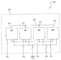
도 2를 참조하여, 본 발명의 일 실시예(200)에서, 종래의 MCP(100)와 같이 동일한 tFAW 규격을 모두 갖는, LPDDR2 기능을 가지는 4개의 다이(202, 203, 204 및 205)는 단일 MCP(201)에서 함께 패키징된다고 가정한다. 이러한 다이는 와이어 본드 패드의 추가에 의해, 또는 공통 버스(207)를 통한 내부 Vpp 전압 공급에 대한 개별적인 TSV 범프 연결(212, 213, 214 및 215)에 의해 변형된다. 제 2 실시예는 유사한 방식으로 Vbb 또는 Vdd/2와 같은 다른 내부 전압 공급에 대한 연결을 제공한다. 모든 다이(202, 203, 204 및 205)의 전원이 평행할 경우 회로 구성요소의 크기상의 감소가 일어날 수 있다.
MCP 인클로져 또는 인캡슐레이션(enclosure or encapsulation) 내에서, 각각의 다이(202, 203, 204 및 205)에 대한 내부 Vpp 공급 노드(212, 213, 214 및 215)는 버스(207)에 함께 와이어링된다. 각각의 다이(202, 203, 204 및 205)가 50ns tFAW 윈도우 내의 4개의 뱅크를 활성하기에 충분한 Vpp 전류를 제공하는 것이 가능하다고 가정하면, 4개의 다이 사이의 16개의 뱅크의 분포에 관계 없이 4개의 다이 적층(200)은 tFAW 윈도우 내에서 16개의 뱅크 활성화를 지원할 수 있다. 이것은, 더 큰 내부 공급을 위한 임의의 추가적인 다이 영역 패널티 없이 성능상의 상당한 증대를 야기할 수 있다.
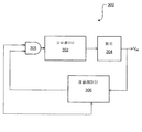
도 3은 종래의 Vpp 펌프 회로(300)의 블록 다이어그램이다. 용량성 펌프 회로는 Vdd 공급으로부터 전류를 유입하고 Vdd보다 더 높은 전위로 레벨을 상승한다. 회로의 간단한 형태는 Vdd 레벨의 2배에 가까운 Vpp 레벨을 성취할 수 있다. 2x Vdd보다 더 높은 전압 레벨을 성취하는 더 복잡한 회로가 업계에 알려져있다. Vdd 펌프(미도시)는 유사한 구조를 갖는다.
오실레이터(302)는 용량성 펌프(304)를 제어하기 위한 클록 신호를 생성한다. 각각의 클록 사이클 상에서, 다량의 전하는 Vpp 레벨을 증가시키기 위하여 출력에 전해진다. 종종, 저장 커페시터는 전하를 홀드하고 각각의 클록 사이클 상에서 전하를 덤핑함으로써 전압 단계를 약화시키기 위하여 출력에 연결되고, 이러한 커패시터는 다소 커져서 집적 회로 칩 상에서 상당한 공간을 차지할 수 있다. 레귤레이터(306)는 언제 Vpp가 바람직한 레벨에 도달할지 결정하기 위해 Vpp의 레벨을 감지한다. 이것이 일어나면, 레귤레이터(306) 출력이 낮아져서 오실레이터(302) 및 펌프(304)를 디스에이블한다. Vpp공급은 EN 입력 신호로 인에이블되거나 디스에이블될 수 있다. 메모리의 데이터가 유지될 필요가 없는 심한 전력 저하 모드에서, EN 입력 신호가 낮아져서 레귤레이터(306)를 직접 디스에이블하여 AND 게이트(308)로 오실레이터(302) 및 펌프(304)를 턴오프할 수 있다. 동작 중에, Vpp 레벨이 바람직한 레벨 미만일 때, 모든 3개의 블록(302, 304 및 306)은 전력을 소비한다. Vpp가 바람직한 레벨에 도달하면, 오직 레귤레이터(306)만이 전력을 소비한다. 심한 전력 저하 모드에서, 레귤레이터(306)는 EN 입력 신호에 의해 완전히 턴오프되어 전력을 절약한다.
제 3 실시예에서, 오직 하나의 다이의 레귤레이터는 남은 레귤레이터가 디스에이블 될 동안 인에이블된다. 이것은, 휴대전화와 같은 핸드헬드(handheld) 휴대용 장치에서 특히 중요한 셀프 리프레시 데이터 리텐션 모드에서 전력을 상당히 절감시킬 수 있다.
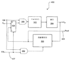
도 4는 본 발명의 제 3 실시예에 적합한 스위칭가능한 전원(400)의 블록 다이어그램이다. Vpp 공급(400)은 추가 입력 ENR(407)을 가져서 레귤레이터(306)를 인에이블한다. ENR(407)이 하이 레벨 1일 경우, 회로는 도 3의 Vpp 공급과 동일하게 기능한다. 이러한 실시예에서, 레귤레이터(306)는 ENR 입력(407) 상의 로우 레벨 신호0에 의해 디스에이블될 수 있다. ENR 입력(407)은 AND 게이트(402) 상의 하나의 입력에 연결되고, 그 결과 신호 0이 ENR상에 있을 때 레귤레이터(306)를 디스에이블한다. 추가적으로, 외부로 제공된 레귤레이터 입력(RIN(406))은 오실레이터(302) 및 펌프(304)를 제어하기 위해 다중화기(404)를 통해 연결된다. Vpp 공급(400)은 또한 Rout 단자(408) 상에서 로컬 레귤레이터 출력을 제공한다.
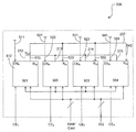
도 5를 참조하면, 본 발명의 제 3 실시예는 도 4의 전원을 통합한다. 도 1과 같이, 각각의 다이(501, 502, 503 및 504)의 내부 Vpp 공급 노드(212, 213, 214 및 215)는 MCP(500)의 버스(207)에 함께 와이어링된다. 그러나, 이러한 실시예에서 LPDDR2 다이 #1(501)은 ENR 입력(512)에 인가된 로직 하이 1(511) 또는 Vdd 레벨의 결과로 인에이블된 레귤레이터를 가지고, LPDDR2 다이 #2(502), #3(503) 및 #4(504)는 각각 라인(521, 531 및 541) 상의 로직 로우 0나 또는 상응하는 ENR 입력(522, 532 및 542)에 인가된 Vss 레벨의 결과로 디스에이블된 레귤레이터를 갖는다. 다이 #1 상의 레귤레이터 출력 ROUT(513)은 다이 #2(502), #3(503) 및 #4(504) 상의 레귤레이터 입력(523, 533 및 543) RIN에 각각 연결된다. 결과적으로, MCP(500) 내의 오직 하나의 레귤레이터(LPDDR2 다이 #1(501) 상의 레귤레이터)가 인에이블되고 전력 소비량이 감소된다. 이전처럼, 다이(501, 502, 503 및 504) 상의 모든 Vpp 펌프는 다수의 뱅크가 짧은 시간의 기간 이내에 활성화될 때처럼 Vpp에 대한 전류 드라이브 요건을 충족시켜야 할 때 활성화될 수 있다. 이러한 기법은 Vbb 기판 바이어스 공급과 같이 MCP DRAM의 다른 공급에 또한 적용될 수 있다. 이것은 또한 Vprog 또는 Vers 전하 펌프와 같은 MCP 구성의 NAND 플래시 장치 상의 내부 공급에 적용될 수도 있다.
Vpp와 같이 펌핑된 공급은 문제없이 함께 집단을 이룰 수 있다. 이러한 경우에, 각각의 장치가 자신의 레귤레이터를 인에이블하면, 장치 간의 변화로 인하여, 각각의 레귤레이터는 다소 상이한 전압에서 펌프를 디스에이블 할 수 있다. 필수적으로, 최고 임계값을 갖는 레귤레이터는 결합된 시스템의 전체 Vpp 레벨을 결정할 것이다. Vpp 공급의 레귤레이터는 임계값 지점에 정확하게 전압을 확립하기 위해 전형적으로 초과 전하를 드레인오프하지 않으므로, 전력은 레귤레이터 임계 레벨의 일부 변화를 가짐으로써 낭비되지 않는다.
도 6은 본 발명의 방법의 흐름도이다. 상기 기재된 바와 같이, 제 1 단계는 내부 전원에 연결된 별개의 메모리 장치상에 단자를 제공하는 단계이다. 선행 기술 장치에서, 이러한 연결은 다른 구성요소에 접근불가능하다. 기재된 바와 같이, 이러한 방법은 DRAM, NOR 플래시, NAND 플래시를 포함하는 플래시 메모리, PCRAM(상 변화 랜덤 액세스 메모리) 및 내부 전원을 포함하는 임의의 메모리 소자와 같은 다양한 장치로 동작할 것이다.
다음 단계는 장치가 전력을 공유하는 것을 허용하는 장치의 단자를 연결하는 단계다. 도 1에서 도시된 바와 같은 간단한 실시예는 종료된다. 동일한 프로세스는 Vbb 기판 바이어스 공급과 같은 MCP DRAM의 공급과 같은 메모리 장치 내부의 다른 전압을 연결하기 위해 지속될 수 있다. 이것은 또한 Vprog 또는 Vers 전하 펌프와 같은 MCP 구조의 NAND 플래시 장치 상의 내부 공급에 적용될 수 있다.
이 프로세스는 자신의 내부 전원의 내부 레귤레이터를 갖는 장치에서 지속된다. 이러한 경우에, 이 장치는 레귤레이터 입력 및/또는 레귤레이터 출력 연결이 제공될 수 있다. 제 1 장치의 레귤레이터 출력 연결은 적어도 하나 및 종종 다수의 장치의 레귤레이터 입력에 연결된다. 상기 기재된 바와 같이, 이것은 제 1 장치가 다른 장치의 레귤레이터를 스위치 온 및 오프하게 하여 전력을 절감하고 열 축적을 감소시키도록 허용한다.
도면이 Vpp 공급의 공유만 도시하였으나, 내부 공급의 임의의 결합이나 모든 내부 공급이 MCP 인클로져 내에서 공규되어 성능을 향상시키고 전력 소비량을 감소시키고 각각의 별개의 다이 내의 다이 영역을 최적화할 수 있다. 이러한 기법은 DRAM, NAND 플래시 및 NOR 플래시를 포함하는 플래시 메모리뿐만 아니라 PCRAM(상변화 랜덤 액세스 메모리)과 같은 다른 형태의 메모리 및 기타 최근 생겨난 메모리 기술에 적용될 수 있다.
Claims (33)
- 멀티칩 패키지로서,
복수의 메모리 장치를 포함하고,
각각의 메모리 장치는 내부 공급 전압 단자에 연결된 내부 공급 전압 생성기를 더 포함하고, 상기 각각의 메모리 장치의 내부 공급 전압 단자는 상기 멀티칩 패키지 내에서 함께 연결되는, 멀티칩 패키지. - 청구항 1에 있어서, 상기 메모리 장치는 DRAM 장치인, 멀티칩 패키지.
- 청구항 2에 있어서, 상기 내부 공급 전압 생성기는 워드라인 공급 전압 생성기인, 멀티칩 패키지.
- 청구항 2에 있어서, 상기 내부 공급 전압 생성기는 기판 바이어스 공급 전압 생성기인, 멀티칩 패키지.
- 청구항 1에 있어서, 상기 메모리 장치는 플래시 메모리 장치인, 멀티칩 패키지.
- 청구항 5에 있어서, 상기 플래시 메모리 장치는 NAND 플래시 장치인, 멀티칩 패키지.
- 청구항 6에 있어서, 상기 내부 공급 전압 생성기는 페이지 프로그램 공급 전압 생성기인, 멀티칩 패키지.
- 청구항 6에 있어서, 상기 내부 공급 전압 생성기는 블록 소거 공급 전압 생성기인, 멀티칩 패키지.
- 청구항 1에 있어서, 상기 내부 공급 전압 생성기는
레귤레이터 출력 단자, 레귤레이터 입력 단자 및 레귤레이터 인에이블 단자에 연결된 레귤레이터를 더 포함하고, 상기 제 1 메모리 장치의 상기 레귤레이터 인에이블 단자는 상기 제 1 장치의 상기 레귤레이터를 인에이블하기 위해 상기 멀티칩 패키지 내에서 제 1 전압에 연결되고, 제 2 메모리 장치의 상기 레귤레이터 인에이블 단자는 상기 제 2 장치의 상기 레귤레이터를 디스에이블하기 위해 상기 멀티칩 패키지 내에서 제 2 전압에 연결되는, 멀티칩 패키지. - 청구항 9에 있어서, 상기 제 1 메모리 장치의 상기 레귤레이터 출력 단자는 제 2 메모리 장치의 상기 레귤레이터 입력 단자에 연결되는, 멀티칩 패키지.
- 멀티칩 패키지를 구성하는 방법으로서, 내부 공급 전압 단자에 연결된 내부 공급 전압 생성기를 각각 갖는 복수의 메모리 장치를 제공하는 단계와 상기 멀티칩 패키지 내에서 각각의 메모리 장치의 내부 공급 전압 단자를 함께 연결하는 단계를 포함하는, 방법.
- 청구항 11에 있어서, 상기 메모리 장치는 DRAM 장치인, 방법.
- 청구항 12에 있어서, 상기 내부 공급 전압 생성기는 워드라인 공급 전압 생성기인, 방법.
- 청구항 12에 있어서, 상기 내부 공급 전압 생성기는 기판 바이어스 공급 전압 생성기인, 방법.
- 청구항 11에 있어서, 상기 메모리 장치는 플래시 메모리 장치인, 방법.
- 청구항 15에 있어서, 상기 플래시 메모리 장치는 NAND 플래시 장치인, 방법.
- 청구항 16에 있어서, 상기 내부 공급 전압 생성기는 페이지 프로그램 공급 전압 생성기인, 방법.
- 청구항 16에 있어서, 상기 내부 공급 전압 생성기는 블록 소거 공급 전압 생성기인, 방법.
- 청구항 11에 있어서, 상기 내부 공급 전압 생성기는 레귤레이터 출력 단자, 레귤레이터 입력 단자 및 레귤레이터 인에이블 단자에 연결된 레귤레이터를 더 포함하고, 상기 방법은 상기 멀티칩 패키지 내에서 상기 제 1 메모리 장치의 레귤레이터 인에이블 단자를 상기 제 1 장치의 상기 레귤레이터를 인에이블하기 위한 제 1 전압에 연결하는 단계 및 상기 멀티칩 패키지 내에서 제 2 메모리 장치의 레귤레이터 인에이블 단자를 상기 제 2 장치의 레귤레이터를 디스에이블하기 위한 제 2 전압에 연결하는 단계를 더 포함하는, 방법.
- 청구항 19에 있어서, 상기 제 1 메모리 장치의 레귤레이터 출력 단자를 상기 제 2 메모리 장치의 레귤레이터 입력 단자에 연결하는 단계를 더 포함하는, 방법.
- 공통 패키지에서 적어도 하나의 다른 집적 회로 장치와 내부 전원을 공유하기 위해 적응된 상기 내부 전원을 갖는 집적 회로 장치로서, 상기 적응은 상기 내부 전원에 대한 제 1 외부 연결을 포함하는, 집적회로 장치.
- 청구항 21에 있어서, 상기 제 1 외부 연결은 와이어 본드 패드와 TSV 범프의 그룹으로부터 선택되는, 집적 회로 장치.
- 청구항 21에 있어서, 상기 제 1 연결과는 상이한 전위를 갖는, 상기 내부 전원에 대한 제 2 연결을 더 포함하는, 집적 회로 장치.
청구항 21에 있어서, 상기 전원의 레귤레이터 및 다른 유사한 집적 회로의 상기 레귤레이터를 디스에이블하기 위한 상기 내부 전원에 대한 제 2 연결을 더 포함하는, 집적 회로 장치. - 시스템으로서,
멀티칩 패키지의 복수의 메모리 장치를 포함하고, 각각의 메모리 장치는 내부 공급 전압 단자에 연결된 내부 공급 전압 생성기를 더 포함하고, 상기 각각의 메모리 장치의 내부 공급 전압 단자는 상기 멀티칩 패키지 내에서 함께 연결되는, 시스템. - 청구항 23에 있어서, 상기 메모리 장치는 DRAM 장치인, 시스템.
- 청구항 24에 있어서, 상기 내부 공급 전압 생성기는 워드라인 공급 전압 생성기인, 시스템.
- 청구항 24에 있어서, 상기 내부 공급 전압 생성기는 기판 바이어스 공급 전압 생성기인, 시스템.
- 청구항 24에 있어서, 상기 메모리 장치는 플래시 메모리 장치인, 시스템.
- 청구항 27에 있어서, 상기 플래시 메모리 장치는 NAND 플래시 장치인, 시스템.
- 청구항 28에 있어서, 상기 내부 공급 전압 생성기는 페이지 프로그램 공급 전압 생성기인, 시스템.
- 청구항 28에 있어서, 상기 내부 공급 전압 생성기는 블록 소거 공급 전압 생성기인, 시스템.
- 청구항 23에 있어서, 상기 내부 공급 전압 생성기는,
레귤레이터 출력 단자, 레귤레이터 입력 단자 및 레귤레이터 인에이블 단자에 연결된 레귤레이터를 더 포함하고, 상기 제 1 메모리 장치의 상기 레귤레이터 인에이블 단자는 상기 멀티칩 패키지내에서 상기 제 1 장치의 상기 레귤레이터를 인에이블하기 위한 제 1 전압에 연결되고, 제 2 메모리 장치의 상기 레귤레이터 인에이블 단자는 상기 멀티칩 패키지내에서 상기 제 2 장치의 상기 레귤레이터를 디스에이블하기 위한 제 2 전압에 연결되는, 시스템. - 청구항 31에 있어서, 상기 제 1 메모리 장치의 상기 레귤레이터 출력 단자는 상기 제 2 메모리 장치의 상기 레귤레이터 입력 단자에 연결되는, 시스템.
Applications Claiming Priority (3)
| Application Number | Priority Date | Filing Date | Title |
|---|---|---|---|
| US41643710P | 2010-11-23 | 2010-11-23 | |
| US61/416,437 | 2010-11-23 | ||
| PCT/CA2011/000528 WO2012068664A1 (en) | 2010-11-23 | 2011-05-03 | Method and apparatus for sharing internal power supplies in integrated circuit devices |
Publications (1)
| Publication Number | Publication Date |
|---|---|
| KR20130140782A true KR20130140782A (ko) | 2013-12-24 |
Family
ID=46064267
Family Applications (1)
| Application Number | Title | Priority Date | Filing Date |
|---|---|---|---|
| KR1020137015142A KR20130140782A (ko) | 2010-11-23 | 2011-05-03 | 집적 회로 장치에서 내부 전원을 공유하기 위한 방법 및 장치 |
Country Status (7)
| Country | Link |
|---|---|
| US (2) | US8625352B2 (ko) |
| EP (1) | EP2643835A1 (ko) |
| JP (1) | JP5623653B2 (ko) |
| KR (1) | KR20130140782A (ko) |
| CN (1) | CN103229240B (ko) |
| HK (1) | HK1186569A1 (ko) |
| WO (1) | WO2012068664A1 (ko) |
Families Citing this family (4)
| Publication number | Priority date | Publication date | Assignee | Title |
|---|---|---|---|---|
| US8913443B2 (en) * | 2011-09-19 | 2014-12-16 | Conversant Intellectual Property Management Inc. | Voltage regulation for 3D packages and method of manufacturing same |
| US9318186B1 (en) * | 2014-12-31 | 2016-04-19 | Nanya Technology Corporation | DRAM wordline control circuit, DRAM module and method of controlling DRAM wordline voltage |
| TWI560718B (en) * | 2015-03-27 | 2016-12-01 | Silicon Motion Inc | Data storage device and encoding method thereof |
| JP7320291B2 (ja) | 2021-07-12 | 2023-08-03 | 有限会社 エコ・ライス新潟 | 液体冷凍保存用容器及び飲料の長期保存方法 |
Family Cites Families (23)
| Publication number | Priority date | Publication date | Assignee | Title |
|---|---|---|---|---|
| US5197029A (en) * | 1991-02-07 | 1993-03-23 | Texas Instruments Incorporated | Common-line connection for integrated memory array |
| JPH1070243A (ja) * | 1996-05-30 | 1998-03-10 | Toshiba Corp | 半導体集積回路装置およびその検査方法およびその検査装置 |
| US6750527B1 (en) * | 1996-05-30 | 2004-06-15 | Kabushiki Kaisha Toshiba | Semiconductor integrated circuit device having a plurality of wells, test method of testing the semiconductor integrated circuit device, and test device which executes the test method |
| TW408332B (en) * | 1997-07-29 | 2000-10-11 | Toshiba Corp | Semiconductor memory and method for controlling programming the same |
| KR100399773B1 (ko) | 2001-02-08 | 2003-09-26 | 삼성전자주식회사 | 메모리슬롯별 서로 다른 기준전압을 갖는 반도체 메모리장치 |
| JP2003036673A (ja) * | 2001-07-24 | 2003-02-07 | Mitsubishi Electric Corp | 半導体記憶装置 |
| JP2003132679A (ja) * | 2001-10-23 | 2003-05-09 | Hitachi Ltd | 半導体装置 |
| US7466160B2 (en) * | 2002-11-27 | 2008-12-16 | Inapac Technology, Inc. | Shared memory bus architecture for system with processor and memory units |
| JP4419049B2 (ja) * | 2003-04-21 | 2010-02-24 | エルピーダメモリ株式会社 | メモリモジュール及びメモリシステム |
| JP4068616B2 (ja) * | 2003-12-26 | 2008-03-26 | エルピーダメモリ株式会社 | 半導体装置 |
| KR100626385B1 (ko) * | 2004-09-13 | 2006-09-20 | 삼성전자주식회사 | 반도체 메모리 장치 및 그것을 포함하는 멀티칩 패키지 |
| KR100688514B1 (ko) * | 2005-01-05 | 2007-03-02 | 삼성전자주식회사 | 다른 종류의 mcp를 탑재한 메모리 모듈 |
| JP2006286048A (ja) * | 2005-03-31 | 2006-10-19 | Toshiba Corp | 半導体記憶装置 |
| US7499345B2 (en) * | 2005-11-25 | 2009-03-03 | Giovanni Campardo | Non-volatile memory implemented with low-voltages transistors and related system and method |
| JP2007180087A (ja) * | 2005-12-27 | 2007-07-12 | Seiko Epson Corp | 集積回路装置 |
| KR100798797B1 (ko) * | 2006-06-30 | 2008-01-29 | 주식회사 하이닉스반도체 | 내부전압 발생장치를 구비하는 반도체메모리소자 및 그의구동방법 |
| US7639540B2 (en) * | 2007-02-16 | 2009-12-29 | Mosaid Technologies Incorporated | Non-volatile semiconductor memory having multiple external power supplies |
| CN101290896A (zh) * | 2007-04-19 | 2008-10-22 | 矽品精密工业股份有限公司 | 可供堆叠的半导体装置及其制法 |
| JP2008300469A (ja) * | 2007-05-30 | 2008-12-11 | Sharp Corp | 不揮発性半導体記憶装置 |
| KR101488383B1 (ko) * | 2007-12-21 | 2015-02-02 | 샌디스크 테크놀로지스, 인코포레이티드 | 자체 구성 가능한 다중 레귤레이터 asic 코어 전력 전달 |
| WO2009085439A1 (en) | 2007-12-21 | 2009-07-09 | Sandisk Corporation | Multi-regulator power delivery system for asic cores |
| US7894230B2 (en) | 2009-02-24 | 2011-02-22 | Mosaid Technologies Incorporated | Stacked semiconductor devices including a master device |
| US8400781B2 (en) * | 2009-09-02 | 2013-03-19 | Mosaid Technologies Incorporated | Using interrupted through-silicon-vias in integrated circuits adapted for stacking |
-
2011
- 2011-05-03 CN CN201180056159.XA patent/CN103229240B/zh not_active Expired - Fee Related
- 2011-05-03 KR KR1020137015142A patent/KR20130140782A/ko not_active Application Discontinuation
- 2011-05-03 US US13/099,791 patent/US8625352B2/en active Active
- 2011-05-03 JP JP2013540186A patent/JP5623653B2/ja not_active Expired - Fee Related
- 2011-05-03 WO PCT/CA2011/000528 patent/WO2012068664A1/en active Application Filing
- 2011-05-03 EP EP11843041.2A patent/EP2643835A1/en not_active Withdrawn
-
2013
- 2013-12-12 HK HK13113852.5A patent/HK1186569A1/xx not_active IP Right Cessation
-
2014
- 2014-01-06 US US14/148,336 patent/US9236095B2/en active Active
Also Published As
| Publication number | Publication date |
|---|---|
| US8625352B2 (en) | 2014-01-07 |
| CN103229240A (zh) | 2013-07-31 |
| US9236095B2 (en) | 2016-01-12 |
| US20120127798A1 (en) | 2012-05-24 |
| JP5623653B2 (ja) | 2014-11-12 |
| CN103229240B (zh) | 2015-05-20 |
| EP2643835A1 (en) | 2013-10-02 |
| WO2012068664A1 (en) | 2012-05-31 |
| HK1186569A1 (en) | 2014-03-14 |
| US20140119136A1 (en) | 2014-05-01 |
| JP2014501016A (ja) | 2014-01-16 |
Similar Documents
| Publication | Publication Date | Title |
|---|---|---|
| US10020046B1 (en) | Stack refresh control for memory device | |
| US10431292B2 (en) | Method and apparatus for controlling access to a common bus by multiple components | |
| KR100715147B1 (ko) | 전류소모를 감소시키는 내부전원전압 발생회로를 가지는멀티칩 반도체 메모리 장치 | |
| US20210216224A1 (en) | Memory module capable of reducing power consumption and semiconductor system including the same | |
| JP2002032987A (ja) | 内部電圧発生回路 | |
| US10097086B2 (en) | Fast ramp low supply charge pump circuits | |
| US9236095B2 (en) | Method and apparatus for sharing internal power supplies in integrated circuit devices | |
| US20170154666A1 (en) | Semiconductor memory device for diminishing peak current in multi-die memory structure | |
| US11740683B2 (en) | Power management | |
| KR20120108474A (ko) | 반도체 장치 | |
| US10607660B2 (en) | Nonvolatile memory device and operating method of the same | |
| KR20180007288A (ko) | 메모리 장치, 이를 포함하는 메모리 시스템 및 메모리 시스템의 동작 방법 | |
| US9792970B2 (en) | Semiconductor device and semiconductor system | |
| US9721623B2 (en) | Memory apparatus using plurality of power sources and system including the same | |
| US8687439B2 (en) | Semiconductor apparatus and memory system including the same | |
| KR101654487B1 (ko) | 반도체 메모리 장치 | |
| CN105632545A (zh) | 一种3d内存芯片 | |
| US20190073020A1 (en) | Dynamic memory offlining and voltage scaling | |
| US20090257272A1 (en) | Reduced size charge pump for dram system | |
| JP6214520B2 (ja) | 半導体回路装置 | |
| KR100238239B1 (ko) | 반도체 메모리 장치의 승압 전압 발생기 | |
| US10848059B1 (en) | Systems and methods involving charge pumps coupled with external pump capacitors and other circuitry | |
| US20230011582A1 (en) | Memory module including module substrate | |
| KR102477269B1 (ko) | 다수의 파워 레일들을 갖는 메모리 장치 및 그 동작방법 | |
| CN114038491A (zh) | 3d动态存储装置及读数据方法、写数据方法、内存设备 |
Legal Events
| Date | Code | Title | Description |
|---|---|---|---|
| WITN | Application deemed withdrawn, e.g. because no request for examination was filed or no examination fee was paid |