KR20130140407A - 미세 피치 pcb 기판에 솔더 범프 형성 방법 및 이를 이용한 반도체 소자의 플립 칩 본딩 방법 - Google Patents
미세 피치 pcb 기판에 솔더 범프 형성 방법 및 이를 이용한 반도체 소자의 플립 칩 본딩 방법 Download PDFInfo
- Publication number
- KR20130140407A KR20130140407A KR1020120063792A KR20120063792A KR20130140407A KR 20130140407 A KR20130140407 A KR 20130140407A KR 1020120063792 A KR1020120063792 A KR 1020120063792A KR 20120063792 A KR20120063792 A KR 20120063792A KR 20130140407 A KR20130140407 A KR 20130140407A
- Authority
- KR
- South Korea
- Prior art keywords
- solder
- paste
- sbm
- solder bump
- pcb substrate
- Prior art date
- Legal status (The legal status is an assumption and is not a legal conclusion. Google has not performed a legal analysis and makes no representation as to the accuracy of the status listed.)
- Granted
Links
Images


Classifications
-
- H—ELECTRICITY
- H10—SEMICONDUCTOR DEVICES; ELECTRIC SOLID-STATE DEVICES NOT OTHERWISE PROVIDED FOR
- H10W—GENERIC PACKAGES, INTERCONNECTIONS, CONNECTORS OR OTHER CONSTRUCTIONAL DETAILS OF DEVICES COVERED BY CLASS H10
- H10W72/00—Interconnections or connectors in packages
- H10W72/071—Connecting or disconnecting
- H10W72/072—Connecting or disconnecting of bump connectors
-
- H—ELECTRICITY
- H10—SEMICONDUCTOR DEVICES; ELECTRIC SOLID-STATE DEVICES NOT OTHERWISE PROVIDED FOR
- H10W—GENERIC PACKAGES, INTERCONNECTIONS, CONNECTORS OR OTHER CONSTRUCTIONAL DETAILS OF DEVICES COVERED BY CLASS H10
- H10W72/00—Interconnections or connectors in packages
- H10W72/01—Manufacture or treatment
- H10W72/012—Manufacture or treatment of bump connectors, dummy bumps or thermal bumps
-
- H—ELECTRICITY
- H10—SEMICONDUCTOR DEVICES; ELECTRIC SOLID-STATE DEVICES NOT OTHERWISE PROVIDED FOR
- H10W—GENERIC PACKAGES, INTERCONNECTIONS, CONNECTORS OR OTHER CONSTRUCTIONAL DETAILS OF DEVICES COVERED BY CLASS H10
- H10W72/00—Interconnections or connectors in packages
- H10W72/20—Bump connectors, e.g. solder bumps or copper pillars; Dummy bumps; Thermal bumps
-
- H—ELECTRICITY
- H10—SEMICONDUCTOR DEVICES; ELECTRIC SOLID-STATE DEVICES NOT OTHERWISE PROVIDED FOR
- H10W—GENERIC PACKAGES, INTERCONNECTIONS, CONNECTORS OR OTHER CONSTRUCTIONAL DETAILS OF DEVICES COVERED BY CLASS H10
- H10W72/00—Interconnections or connectors in packages
- H10W72/30—Die-attach connectors
-
- H—ELECTRICITY
- H10—SEMICONDUCTOR DEVICES; ELECTRIC SOLID-STATE DEVICES NOT OTHERWISE PROVIDED FOR
- H10W—GENERIC PACKAGES, INTERCONNECTIONS, CONNECTORS OR OTHER CONSTRUCTIONAL DETAILS OF DEVICES COVERED BY CLASS H10
- H10W72/00—Interconnections or connectors in packages
- H10W72/01—Manufacture or treatment
- H10W72/012—Manufacture or treatment of bump connectors, dummy bumps or thermal bumps
- H10W72/01231—Manufacture or treatment of bump connectors, dummy bumps or thermal bumps using blanket deposition
- H10W72/01236—Manufacture or treatment of bump connectors, dummy bumps or thermal bumps using blanket deposition in solid form, e.g. by using a powder or by laminating a foil
-
- H—ELECTRICITY
- H10—SEMICONDUCTOR DEVICES; ELECTRIC SOLID-STATE DEVICES NOT OTHERWISE PROVIDED FOR
- H10W—GENERIC PACKAGES, INTERCONNECTIONS, CONNECTORS OR OTHER CONSTRUCTIONAL DETAILS OF DEVICES COVERED BY CLASS H10
- H10W72/00—Interconnections or connectors in packages
- H10W72/01—Manufacture or treatment
- H10W72/012—Manufacture or treatment of bump connectors, dummy bumps or thermal bumps
- H10W72/01271—Cleaning, e.g. oxide removal or de-smearing
-
- H—ELECTRICITY
- H10—SEMICONDUCTOR DEVICES; ELECTRIC SOLID-STATE DEVICES NOT OTHERWISE PROVIDED FOR
- H10W—GENERIC PACKAGES, INTERCONNECTIONS, CONNECTORS OR OTHER CONSTRUCTIONAL DETAILS OF DEVICES COVERED BY CLASS H10
- H10W72/00—Interconnections or connectors in packages
- H10W72/071—Connecting or disconnecting
- H10W72/072—Connecting or disconnecting of bump connectors
- H10W72/07211—Treating the bond pad before connecting, e.g. by applying flux or cleaning
-
- H—ELECTRICITY
- H10—SEMICONDUCTOR DEVICES; ELECTRIC SOLID-STATE DEVICES NOT OTHERWISE PROVIDED FOR
- H10W—GENERIC PACKAGES, INTERCONNECTIONS, CONNECTORS OR OTHER CONSTRUCTIONAL DETAILS OF DEVICES COVERED BY CLASS H10
- H10W72/00—Interconnections or connectors in packages
- H10W72/071—Connecting or disconnecting
- H10W72/072—Connecting or disconnecting of bump connectors
- H10W72/07231—Techniques
- H10W72/07236—Soldering or alloying
-
- H—ELECTRICITY
- H10—SEMICONDUCTOR DEVICES; ELECTRIC SOLID-STATE DEVICES NOT OTHERWISE PROVIDED FOR
- H10W—GENERIC PACKAGES, INTERCONNECTIONS, CONNECTORS OR OTHER CONSTRUCTIONAL DETAILS OF DEVICES COVERED BY CLASS H10
- H10W72/00—Interconnections or connectors in packages
- H10W72/071—Connecting or disconnecting
- H10W72/073—Connecting or disconnecting of die-attach connectors
-
- H—ELECTRICITY
- H10—SEMICONDUCTOR DEVICES; ELECTRIC SOLID-STATE DEVICES NOT OTHERWISE PROVIDED FOR
- H10W—GENERIC PACKAGES, INTERCONNECTIONS, CONNECTORS OR OTHER CONSTRUCTIONAL DETAILS OF DEVICES COVERED BY CLASS H10
- H10W72/00—Interconnections or connectors in packages
- H10W72/20—Bump connectors, e.g. solder bumps or copper pillars; Dummy bumps; Thermal bumps
- H10W72/241—Dispositions, e.g. layouts
- H10W72/245—Dispositions, e.g. layouts of outermost layers of multilayered bumps, e.g. bump coating being only on a part of a bump core
-
- H—ELECTRICITY
- H10—SEMICONDUCTOR DEVICES; ELECTRIC SOLID-STATE DEVICES NOT OTHERWISE PROVIDED FOR
- H10W—GENERIC PACKAGES, INTERCONNECTIONS, CONNECTORS OR OTHER CONSTRUCTIONAL DETAILS OF DEVICES COVERED BY CLASS H10
- H10W72/00—Interconnections or connectors in packages
- H10W72/20—Bump connectors, e.g. solder bumps or copper pillars; Dummy bumps; Thermal bumps
- H10W72/251—Materials
- H10W72/252—Materials comprising solid metals or solid metalloids, e.g. PbSn, Ag or Cu
-
- H—ELECTRICITY
- H10—SEMICONDUCTOR DEVICES; ELECTRIC SOLID-STATE DEVICES NOT OTHERWISE PROVIDED FOR
- H10W—GENERIC PACKAGES, INTERCONNECTIONS, CONNECTORS OR OTHER CONSTRUCTIONAL DETAILS OF DEVICES COVERED BY CLASS H10
- H10W72/00—Interconnections or connectors in packages
- H10W72/20—Bump connectors, e.g. solder bumps or copper pillars; Dummy bumps; Thermal bumps
- H10W72/251—Materials
- H10W72/255—Materials of outermost layers of multilayered bumps, e.g. material of a coating
-
- H—ELECTRICITY
- H10—SEMICONDUCTOR DEVICES; ELECTRIC SOLID-STATE DEVICES NOT OTHERWISE PROVIDED FOR
- H10W—GENERIC PACKAGES, INTERCONNECTIONS, CONNECTORS OR OTHER CONSTRUCTIONAL DETAILS OF DEVICES COVERED BY CLASS H10
- H10W72/00—Interconnections or connectors in packages
- H10W72/30—Die-attach connectors
- H10W72/321—Structures or relative sizes of die-attach connectors
- H10W72/325—Die-attach connectors having a filler embedded in a matrix
-
- H—ELECTRICITY
- H10—SEMICONDUCTOR DEVICES; ELECTRIC SOLID-STATE DEVICES NOT OTHERWISE PROVIDED FOR
- H10W—GENERIC PACKAGES, INTERCONNECTIONS, CONNECTORS OR OTHER CONSTRUCTIONAL DETAILS OF DEVICES COVERED BY CLASS H10
- H10W72/00—Interconnections or connectors in packages
- H10W72/30—Die-attach connectors
- H10W72/351—Materials of die-attach connectors
- H10W72/352—Materials of die-attach connectors comprising metals or metalloids, e.g. solders
-
- H—ELECTRICITY
- H10—SEMICONDUCTOR DEVICES; ELECTRIC SOLID-STATE DEVICES NOT OTHERWISE PROVIDED FOR
- H10W—GENERIC PACKAGES, INTERCONNECTIONS, CONNECTORS OR OTHER CONSTRUCTIONAL DETAILS OF DEVICES COVERED BY CLASS H10
- H10W72/00—Interconnections or connectors in packages
- H10W72/30—Die-attach connectors
- H10W72/351—Materials of die-attach connectors
- H10W72/353—Materials of die-attach connectors not comprising solid metals or solid metalloids, e.g. ceramics
- H10W72/354—Materials of die-attach connectors not comprising solid metals or solid metalloids, e.g. ceramics comprising polymers
-
- H—ELECTRICITY
- H10—SEMICONDUCTOR DEVICES; ELECTRIC SOLID-STATE DEVICES NOT OTHERWISE PROVIDED FOR
- H10W—GENERIC PACKAGES, INTERCONNECTIONS, CONNECTORS OR OTHER CONSTRUCTIONAL DETAILS OF DEVICES COVERED BY CLASS H10
- H10W90/00—Package configurations
- H10W90/701—Package configurations characterised by the relative positions of pads or connectors relative to package parts
- H10W90/721—Package configurations characterised by the relative positions of pads or connectors relative to package parts of bump connectors
- H10W90/724—Package configurations characterised by the relative positions of pads or connectors relative to package parts of bump connectors between a chip and a stacked insulating package substrate, interposer or RDL
Landscapes
- Electric Connection Of Electric Components To Printed Circuits (AREA)
Abstract
Description
도 4 내지 도 6은 본 발명의 다른 실시예에 따른 LVSoP가 형성된 PCB 기판에 반도체 소자의 플립 칩 본딩 방법을 설명하기 위한 공정 흐름도,
도 7 및 도 8은 본 발명의 또 다른 실시예에 따른 LVSoP가 형성된 PCB 기판에 반도체 소자의 플립 칩 본딩 방법을 설명하기 위한 공정 흐름도,
도 9는 70um의 직경 및 130um의 피치를 가지는 금속 패드와 약 10um의 두께를 가지는 솔더 마스크가 형성된 PCB 기판의 SEM 사진,
도 10은 도 9의 PCB 기판에 도 1 내지 도 3의 공정을 통해 LVSoP를 형성한 PCB 기판의 SEM 사진,
도 11은 도 9의 LVSoP의 높이를 측정한 그래프,
도 12는 코이닝 공정을 통하여 솔더 마스크의 높이보다 높이가 높은 LVSoP가 평평하게 된 PCB 기판의 SEM 사진이다.
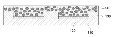
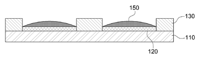
130: 솔더 마스크 140: SBM 페이스트
150: LVSoP
Claims (12)
- 금속 패드 및 솔더 마스크를 포함하는 PCB 기판 전면에 일정한 두께의 SBM(Solder Bump Maker) 페이스트를 도포하는 단계;
상기 SBM 페이스트를 상기 SBM 페이스트에 포함된 솔더의 녹는점보다 높은 온도로 가열한 후 냉각시켜 솔더 범프를 형성하는 단계; 및
상기 SBM 페이스트의 잔여 고분자 수지와 잔여 솔더 입자를 솔벤트를 사용하여 세척하는 단계;
를 포함하는 미세 피치 PCB 기판에 솔더 범프 형성 방법.
- 제1항에 있어서, 상기 솔더 범프를 형성하는 단계에서,
상기 SBM 페이스트의 솔더 입자들이 상기 금속 패드 위에서 젖음 특성을 나타내어 솔더 범프가 형성되는 것을 특징으로 하는 미세 피치 PCB 기판에 솔더 범프 형성 방법.
- 제1항에 있어서,
상기 SBM 페이스트는 SBM 페이스트 100 중량% 기준으로 15 ~ 25 중량%의 고분자 수지, 1 ~ 10 중량%의 환원제 및 50 ~ 80 중량%의 솔더를 포함하는 것을 특징으로 하는 미세 피치 PCB 기판에 솔더 범프 형성 방법.
- 제3항에 있어서,
상기 고분자 수지는 DGEBA, TGDDM, TriTGDDM, 이소시아네이트(Isocyanate), 비스말레이미드(Bismaleimide), 에폭시 변성 실리콘 오일, 아민변성 실리콘 오일, 카복실 변성실리콘 오일 및 폴리올 중 적어도 하나를 포함하는 것을 특징으로 하는 미세 피치 PCB 기판에 솔더 범프 형성 방법.
- 제3항에 있어서,
상기 환원제는 글루타르산(Glutaric Acid), 말산(Malic Acid), 아젤라익산(Azelaic Acid), 아비에트산(Abietic Acid), 아디프산(Adipic Acid), 아스코르빈산(Ascorbic Acid), 아크릴산(Acrylic Acid) 및 시트르산(Citric Acid) 중 적어도 하나를 포함하는 것을 특징으로 하는 미세 피치 PCB 기판에 솔더 범프 형성 방법.
- 제3항에 있어서,
상기 솔더의 입자 크기는 0.1um ~ 70um인 것을 특징으로 하는 미세 피치 PCB 기판에 솔더 범프 형성 방법.
- 제3항에 있어서,
상기 솔더는 Sn, Bi, Ag, Cu, In 및 Pb 중 적어도 하나를 포함하는 것을 특징으로 하는 미세 피치 PCB 기판에 솔더 범프 형성 방법.
- 제1항에 있어서,
상기 솔더 범프가 형성된 PCB 기판에 코이닝 공정을 수행하는 단계;
를 더 포함하는 것을 특징으로 하는 미세 피치 PCB 기판에 솔더 범프 형성 방법.
- 금속 패드 및 솔더 마스크를 포함하는 PCB 기판 전면에 일정한 두께의 SBM(Solder Bump Maker) 페이스트를 도포하는 단계;
상기 SBM 페이스트를 상기 SBM 페이스트에 포함된 솔더의 녹는점보다 높은 온도로 가열한 후 냉각시켜 솔더 범프를 형성하는 단계;
상기 SBM 페이스트의 잔여 고분자 수지와 잔여 솔더 입자를 솔벤트를 사용하여 세척하는 단계;
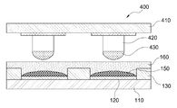
상기 솔더 범프가 형성된 PCB 기판 전면에 산화막 제거를 위한 플럭스를 도포하는 단계;
상기 플럭스가 도포된 PCB 기판에 구리 필러가 형성된 반도체 소자를 플립 칩 본딩하는 단계; 및
잔류 플럭스를 제거하는 단계;
를 포함하는 반도체 소자의 플립 칩 본딩 방법.
- 제9항에 있어서,
상기 구리 필러의 끝단에 솔더 캡 또는 니켈 캡이 형성되어 있는 것을 특징으로 하는 반도체 소자의 플립 칩 본딩 방법.
- 금속 패드 및 솔더 마스크를 포함하는 PCB 기판 전면에 일정한 두께의 SBM(Solder Bump Maker) 페이스트를 도포하는 단계;
상기 SBM 페이스트를 상기 SBM 페이스트에 포함된 솔더의 녹는점보다 높은 온도로 가열한 후 냉각시켜 솔더 범프를 형성하는 단계;
상기 SBM 페이스트의 잔여 고분자 수지와 잔여 솔더 입자를 솔벤트를 사용하여 세척하는 단계;
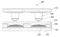
상기 솔더 범프가 형성된 PCB 기판 전면에 산화막 제거 및 언더필 기능을 수행하는 플럭싱 언더필을 도포하는 단계; 및
상기 플럭싱 언더필이 도포된 PCB 기판에 구리 필러가 형성된 반도체 소자를 플립 칩 본딩하는 단계;
를 포함하는 반도체 소자의 플립 칩 본딩 방법.
- 제11항에 있어서,
상기 구리 필러의 끝단에 솔더 캡 또는 니켈 캡이 형성되어 있는 것을 특징으로 하는 반도체 소자의 플립 칩 본딩 방법.
Priority Applications (2)
| Application Number | Priority Date | Filing Date | Title |
|---|---|---|---|
| KR1020120063792A KR101940237B1 (ko) | 2012-06-14 | 2012-06-14 | 미세 피치 pcb 기판에 솔더 범프 형성 방법 및 이를 이용한 반도체 소자의 플립 칩 본딩 방법 |
| US13/760,350 US8794502B2 (en) | 2012-06-14 | 2013-02-06 | Method of forming solder on pad on fine pitch PCB and method of flip chip bonding semiconductor using the same |
Applications Claiming Priority (1)
| Application Number | Priority Date | Filing Date | Title |
|---|---|---|---|
| KR1020120063792A KR101940237B1 (ko) | 2012-06-14 | 2012-06-14 | 미세 피치 pcb 기판에 솔더 범프 형성 방법 및 이를 이용한 반도체 소자의 플립 칩 본딩 방법 |
Publications (2)
| Publication Number | Publication Date |
|---|---|
| KR20130140407A true KR20130140407A (ko) | 2013-12-24 |
| KR101940237B1 KR101940237B1 (ko) | 2019-01-18 |
Family
ID=49754972
Family Applications (1)
| Application Number | Title | Priority Date | Filing Date |
|---|---|---|---|
| KR1020120063792A Active KR101940237B1 (ko) | 2012-06-14 | 2012-06-14 | 미세 피치 pcb 기판에 솔더 범프 형성 방법 및 이를 이용한 반도체 소자의 플립 칩 본딩 방법 |
Country Status (2)
| Country | Link |
|---|---|
| US (1) | US8794502B2 (ko) |
| KR (1) | KR101940237B1 (ko) |
Cited By (3)
| Publication number | Priority date | Publication date | Assignee | Title |
|---|---|---|---|---|
| KR20210076493A (ko) * | 2019-12-16 | 2021-06-24 | 주식회사 노피온 | 열가소성 수지를 포함하는 군집형 이방성 도전 접착 필름, 이를 이용한 솔더 범프의 형성방법 및 접합구조체의 제조방법 |
| KR20210076511A (ko) * | 2019-12-16 | 2021-06-24 | 주식회사 노피온 | 열가소성 수지인 폴리우레탄 수지를 포함하는 이방성 도전 접착제, 이를 이용한 솔더범프의 형성 방법 및 접합구조체의 제조방법 |
| KR20210076619A (ko) * | 2019-12-16 | 2021-06-24 | 주식회사 노피온 | 열가소성 수지인 폴리실록산 수지를 포함하는 이방성 도전 접착제, 이를 이용한 솔더 범프의 형성방법 및 접합구조체의 제조방법 |
Families Citing this family (7)
| Publication number | Priority date | Publication date | Assignee | Title |
|---|---|---|---|---|
| KR102060831B1 (ko) * | 2013-02-27 | 2019-12-30 | 삼성전자주식회사 | 플립 칩 패키징 방법, 그리고 상기 플립 칩 패키징 방법에 적용되는 플럭스 헤드 및 그 제조 방법 |
| US10160066B2 (en) * | 2016-11-01 | 2018-12-25 | GM Global Technology Operations LLC | Methods and systems for reinforced adhesive bonding using solder elements and flux |
| US10741482B2 (en) | 2017-12-29 | 2020-08-11 | Advanced Semiconductor Engineering, Inc. | Semiconductor device package |
| CN110557937B (zh) | 2018-05-31 | 2021-08-06 | 铟泰公司 | 有效抑制在bga组合件的不润湿开口的助焊剂 |
| US11488841B2 (en) * | 2019-02-20 | 2022-11-01 | Electronics And Telecommunications Research Institute | Method for manufacturing semiconductor package |
| US11688706B2 (en) * | 2020-09-15 | 2023-06-27 | Micron Technology, Inc. | Semiconductor device assembly with embossed solder mask having non-planar features and associated methods and systems |
| KR102272987B1 (ko) * | 2021-01-27 | 2021-07-05 | 주식회사 프로이천 | 범프형 프로브카드 |
Citations (4)
| Publication number | Priority date | Publication date | Assignee | Title |
|---|---|---|---|---|
| JPH10107415A (ja) * | 1996-10-02 | 1998-04-24 | Furukawa Electric Co Ltd:The | 半田供給方法 |
| JP2007227788A (ja) * | 2006-02-24 | 2007-09-06 | Kyocer Slc Technologies Corp | 配線基板の製造方法および半田ペースト |
| KR20090011198A (ko) * | 2007-07-25 | 2009-02-02 | 앰코 테크놀로지 코리아 주식회사 | 반도체 패키지 및 그의 제조 방법 |
| KR20100007690A (ko) * | 2008-07-10 | 2010-01-22 | 한국전자통신연구원 | 조성물, 및 이를 이용한 솔더 범프 형성방법 및 플립칩 형성방법 |
Family Cites Families (46)
| Publication number | Priority date | Publication date | Assignee | Title |
|---|---|---|---|---|
| USRE32309E (en) * | 1983-10-31 | 1986-12-16 | Scm Corporation | Fusible powdered metal paste |
| US4619715A (en) * | 1984-09-11 | 1986-10-28 | Scm Corporation | Fusible powdered metal paste |
| JPH03165999A (ja) * | 1989-11-24 | 1991-07-17 | Nippondenso Co Ltd | はんだ付け用水溶性フラックス |
| JPH06125169A (ja) * | 1992-10-13 | 1994-05-06 | Fujitsu Ltd | 予備はんだ法 |
| US5478700A (en) * | 1993-12-21 | 1995-12-26 | International Business Machines Corporation | Method for applying bonding agents to pad and/or interconnection sites in the manufacture of electrical circuits using a bonding agent injection head |
| GB9410128D0 (en) * | 1994-05-20 | 1994-07-06 | Burton Chambers Roderick L | Post arrangement |
| JP3224185B2 (ja) * | 1994-09-29 | 2001-10-29 | 富士通株式会社 | はんだ合金及びはんだ粉末及びはんだペースト及びプリント配線板及び電子部品及びはんだ付け方法及びはんだ付け装置 |
| US5868302A (en) * | 1995-09-06 | 1999-02-09 | Matsushita Electric Industrial Co., Ltd. | Method and apparatus for mounting electronic component |
| DE69737281T2 (de) * | 1996-12-10 | 2007-12-20 | Matsushita Electric Industrial Co., Ltd., Kadoma | Vorrichtung und Verfahren zum Drucken von Lötpaste |
| US7654432B2 (en) | 1997-05-27 | 2010-02-02 | Wstp, Llc | Forming solder balls on substrates |
| US6609652B2 (en) * | 1997-05-27 | 2003-08-26 | Spheretek, Llc | Ball bumping substrates, particuarly wafers |
| JP2000062136A (ja) * | 1998-08-21 | 2000-02-29 | Matsushita Electric Ind Co Ltd | 金属ペーストの印刷方法 |
| US6173887B1 (en) * | 1999-06-24 | 2001-01-16 | International Business Machines Corporation | Method of making electrically conductive contacts on substrates |
| JP3831179B2 (ja) * | 1999-06-29 | 2006-10-11 | 株式会社東芝 | 半導体装置の製造方法およびパターン形成方法 |
| JP3403677B2 (ja) * | 1999-09-06 | 2003-05-06 | マイクロ・テック株式会社 | 半田ボール形成方法 |
| JP2002076589A (ja) * | 2000-08-31 | 2002-03-15 | Hitachi Ltd | 電子装置及びその製造方法 |
| US6845901B2 (en) * | 2002-08-22 | 2005-01-25 | Micron Technology, Inc. | Apparatus and method for depositing and reflowing solder paste on a microelectronic workpiece |
| JP2004174538A (ja) * | 2002-11-26 | 2004-06-24 | Ricoh Co Ltd | はんだ合金材料の製造方法、及びはんだ合金を含むインク組成物 |
| US7059512B2 (en) * | 2002-11-06 | 2006-06-13 | Ricoh Company, Ltd. | Solder alloy material layer composition, electroconductive and adhesive composition, flux material layer composition, solder ball transferring sheet, bump and bump forming process, and semiconductor device |
| US7043830B2 (en) * | 2003-02-20 | 2006-05-16 | Micron Technology, Inc. | Method of forming conductive bumps |
| US20040219774A1 (en) * | 2003-05-02 | 2004-11-04 | Yu-Nung Shen | Method for forming conductive bump and device formed with such a conductive bump |
| JP2005026579A (ja) * | 2003-07-04 | 2005-01-27 | Fujitsu Ltd | ハンダバンプ付き電子部品の実装方法およびこれに用いるフラックスフィル |
| US20050058771A1 (en) * | 2003-09-16 | 2005-03-17 | International Business Machines Corporation | Rolling contact screening method and apparatus |
| JP2005183904A (ja) * | 2003-12-22 | 2005-07-07 | Rohm & Haas Electronic Materials Llc | 電子部品にはんだ領域を形成する方法及びはんだ領域を有する電子部品 |
| US7213739B2 (en) * | 2004-04-02 | 2007-05-08 | Fry's Metals, Inc. | Underfill fluxing curative |
| JP3964911B2 (ja) | 2004-09-03 | 2007-08-22 | 松下電器産業株式会社 | バンプ付き基板の製造方法 |
| JP4740865B2 (ja) * | 2004-09-24 | 2011-08-03 | 学校法人日本大学 | セラミック電子部品の製造方法 |
| JP4512497B2 (ja) * | 2005-01-31 | 2010-07-28 | イビデン株式会社 | コンデンサ内蔵パッケージ基板及びその製法 |
| CN100511618C (zh) * | 2005-03-09 | 2009-07-08 | 松下电器产业株式会社 | 金属粒子分散组合物以及使用了它的方法 |
| CN100495675C (zh) * | 2005-03-17 | 2009-06-03 | 松下电器产业株式会社 | 包括半导体芯片的组装体及其制造方法 |
| EP1865549A4 (en) * | 2005-03-29 | 2012-07-11 | Panasonic Corp | FLIP-CHIP ATTACHING METHOD AND ASSEMBLY PROCESSING |
| KR101175482B1 (ko) * | 2005-04-06 | 2012-08-20 | 파나소닉 주식회사 | 플립 칩 실장 방법 및 범프 형성 방법 |
| EP1996002B1 (en) * | 2006-03-16 | 2017-07-05 | Panasonic Intellectual Property Management Co., Ltd. | Bump forming method and bump forming apparatus |
| KR100765146B1 (ko) | 2006-06-15 | 2007-10-12 | 배상준 | 솔더 페이스트 및 이를 이용한 솔더 범프 형성방법 |
| US20080003804A1 (en) * | 2006-06-29 | 2008-01-03 | Ravi Nalla | Method of providing solder bumps of mixed sizes on a substrate using solder transfer in two stages |
| US7906424B2 (en) * | 2007-08-01 | 2011-03-15 | Advanced Micro Devices, Inc. | Conductor bump method and apparatus |
| US20090057378A1 (en) * | 2007-08-27 | 2009-03-05 | Chi-Won Hwang | In-situ chip attachment using self-organizing solder |
| JP2009220493A (ja) * | 2008-03-18 | 2009-10-01 | Nec Electronics Corp | 金属ペースト印刷方法およびメタルマスク |
| US20100029074A1 (en) | 2008-05-28 | 2010-02-04 | Mackay John | Maskless Process for Solder Bump Production |
| US7867842B2 (en) * | 2008-07-29 | 2011-01-11 | International Business Machines Corporation | Method and apparatus for forming planar alloy deposits on a substrate |
| KR20100060968A (ko) * | 2008-11-28 | 2010-06-07 | 삼성전기주식회사 | 메탈 포스트를 구비한 기판 및 그 제조방법 |
| KR20110036450A (ko) * | 2009-10-01 | 2011-04-07 | 삼성전기주식회사 | 플립칩용 기판의 제조방법 및 이를 이용하여 제조한 플립칩용 기판 |
| KR101234597B1 (ko) * | 2009-10-15 | 2013-02-22 | 한국전자통신연구원 | 플립 칩 본딩 방법 및 그의 구조 |
| KR101061048B1 (ko) * | 2010-02-17 | 2011-09-01 | (주)덕산테코피아 | 솔더 잉크 및 이를 이용한 전자소자 패키지 |
| US8921221B2 (en) * | 2011-06-20 | 2014-12-30 | International Business Machines Corporation | IMS (injection molded solder) with two resist layers forming solder bumps on substrates |
| JP2014004819A (ja) * | 2012-05-28 | 2014-01-16 | Hitachi High-Technologies Corp | パターン形成方法及びその形成装置 |
-
2012
- 2012-06-14 KR KR1020120063792A patent/KR101940237B1/ko active Active
-
2013
- 2013-02-06 US US13/760,350 patent/US8794502B2/en active Active
Patent Citations (4)
| Publication number | Priority date | Publication date | Assignee | Title |
|---|---|---|---|---|
| JPH10107415A (ja) * | 1996-10-02 | 1998-04-24 | Furukawa Electric Co Ltd:The | 半田供給方法 |
| JP2007227788A (ja) * | 2006-02-24 | 2007-09-06 | Kyocer Slc Technologies Corp | 配線基板の製造方法および半田ペースト |
| KR20090011198A (ko) * | 2007-07-25 | 2009-02-02 | 앰코 테크놀로지 코리아 주식회사 | 반도체 패키지 및 그의 제조 방법 |
| KR20100007690A (ko) * | 2008-07-10 | 2010-01-22 | 한국전자통신연구원 | 조성물, 및 이를 이용한 솔더 범프 형성방법 및 플립칩 형성방법 |
Cited By (3)
| Publication number | Priority date | Publication date | Assignee | Title |
|---|---|---|---|---|
| KR20210076493A (ko) * | 2019-12-16 | 2021-06-24 | 주식회사 노피온 | 열가소성 수지를 포함하는 군집형 이방성 도전 접착 필름, 이를 이용한 솔더 범프의 형성방법 및 접합구조체의 제조방법 |
| KR20210076511A (ko) * | 2019-12-16 | 2021-06-24 | 주식회사 노피온 | 열가소성 수지인 폴리우레탄 수지를 포함하는 이방성 도전 접착제, 이를 이용한 솔더범프의 형성 방법 및 접합구조체의 제조방법 |
| KR20210076619A (ko) * | 2019-12-16 | 2021-06-24 | 주식회사 노피온 | 열가소성 수지인 폴리실록산 수지를 포함하는 이방성 도전 접착제, 이를 이용한 솔더 범프의 형성방법 및 접합구조체의 제조방법 |
Also Published As
| Publication number | Publication date |
|---|---|
| KR101940237B1 (ko) | 2019-01-18 |
| US20130334291A1 (en) | 2013-12-19 |
| US8794502B2 (en) | 2014-08-05 |
Similar Documents
| Publication | Publication Date | Title |
|---|---|---|
| KR101940237B1 (ko) | 미세 피치 pcb 기판에 솔더 범프 형성 방법 및 이를 이용한 반도체 소자의 플립 칩 본딩 방법 | |
| JP2807940B2 (ja) | フラックス剤および金属粒子を有する接着剤 | |
| CN101904230B (zh) | 焊料球的无助熔剂微穿孔方法和所得的装置 | |
| EP2427036B1 (en) | Process for production of circuit board | |
| TWI612591B (zh) | 迴焊薄膜、焊料凸塊形成方法、焊料接合的形成方法及半導體裝置 | |
| JP2009158593A (ja) | バンプ構造およびその製造方法 | |
| US9978709B2 (en) | Solder bump stretching method for forming a solder bump joint in a device | |
| WO2014104218A1 (ja) | 電子部品が接合した回路基板の製造方法 | |
| JP4729963B2 (ja) | 電子部品接続用突起電極とそれを用いた電子部品実装体およびそれらの製造方法 | |
| JP4115306B2 (ja) | 半導体装置の製造方法 | |
| KR102006637B1 (ko) | 범프의 형성 방법 및 이를 포함하는 반도체 소자의 형성방법 | |
| KR101988890B1 (ko) | 솔더 온 패드의 제조방법 및 그를 이용한 플립 칩 본딩 방법 | |
| JP2010157693A (ja) | 金属バンプを備えた半導体パッケージ基板 | |
| JP5560713B2 (ja) | 電子部品の実装方法等 | |
| JP2009021465A (ja) | 半導体装置実装構造体およびその製造方法ならびに半導体装置の剥離方法 | |
| CN103000609A (zh) | 凸点制作材料及凸点制备方法 | |
| JP2006100457A (ja) | 電子装置及びその製造方法 | |
| JP4453919B2 (ja) | バンプ電極付き電子部品の製造方法 | |
| TWI878402B (zh) | 連接構造體及連接構造體的製造方法 | |
| JP6136411B2 (ja) | 電子部品の接合方法および電子機器 | |
| JP2006100844A (ja) | バンプ電極付き電子部品 | |
| JP2002171055A (ja) | 電子回路基板と電子部品及び電子回路装置並びにこれらの製造方法 | |
| JP6186884B2 (ja) | 電極、電子部品、電子装置および電極の接合方法 | |
| KR20120041430A (ko) | 플립칩 에스오피 제조방법 | |
| JP2014090216A (ja) | バンプ構造およびその製造方法 |
Legal Events
| Date | Code | Title | Description |
|---|---|---|---|
| PA0109 | Patent application |
St.27 status event code: A-0-1-A10-A12-nap-PA0109 |
|
| R17-X000 | Change to representative recorded |
St.27 status event code: A-3-3-R10-R17-oth-X000 |
|
| PG1501 | Laying open of application |
St.27 status event code: A-1-1-Q10-Q12-nap-PG1501 |
|
| PN2301 | Change of applicant |
St.27 status event code: A-3-3-R10-R13-asn-PN2301 St.27 status event code: A-3-3-R10-R11-asn-PN2301 |
|
| R17-X000 | Change to representative recorded |
St.27 status event code: A-3-3-R10-R17-oth-X000 |
|
| A201 | Request for examination | ||
| PA0201 | Request for examination |
St.27 status event code: A-1-2-D10-D11-exm-PA0201 |
|
| D13-X000 | Search requested |
St.27 status event code: A-1-2-D10-D13-srh-X000 |
|
| D14-X000 | Search report completed |
St.27 status event code: A-1-2-D10-D14-srh-X000 |
|
| E902 | Notification of reason for refusal | ||
| PE0902 | Notice of grounds for rejection |
St.27 status event code: A-1-2-D10-D21-exm-PE0902 |
|
| P11-X000 | Amendment of application requested |
St.27 status event code: A-2-2-P10-P11-nap-X000 |
|
| P13-X000 | Application amended |
St.27 status event code: A-2-2-P10-P13-nap-X000 |
|
| E90F | Notification of reason for final refusal | ||
| PE0902 | Notice of grounds for rejection |
St.27 status event code: A-1-2-D10-D21-exm-PE0902 |
|
| P11-X000 | Amendment of application requested |
St.27 status event code: A-2-2-P10-P11-nap-X000 |
|
| P13-X000 | Application amended |
St.27 status event code: A-2-2-P10-P13-nap-X000 |
|
| E701 | Decision to grant or registration of patent right | ||
| PE0701 | Decision of registration |
St.27 status event code: A-1-2-D10-D22-exm-PE0701 |
|
| GRNT | Written decision to grant | ||
| PR0701 | Registration of establishment |
St.27 status event code: A-2-4-F10-F11-exm-PR0701 |
|
| PR1002 | Payment of registration fee |
St.27 status event code: A-2-2-U10-U11-oth-PR1002 Fee payment year number: 1 |
|
| PG1601 | Publication of registration |
St.27 status event code: A-4-4-Q10-Q13-nap-PG1601 |
|
| PR1001 | Payment of annual fee |
St.27 status event code: A-4-4-U10-U11-oth-PR1001 Fee payment year number: 4 |
|
| PR1001 | Payment of annual fee |
St.27 status event code: A-4-4-U10-U11-oth-PR1001 Fee payment year number: 5 |
|
| PR1001 | Payment of annual fee |
St.27 status event code: A-4-4-U10-U11-oth-PR1001 Fee payment year number: 6 |
|
| PR1001 | Payment of annual fee |
St.27 status event code: A-4-4-U10-U11-oth-PR1001 Fee payment year number: 7 |
|
| P22-X000 | Classification modified |
St.27 status event code: A-4-4-P10-P22-nap-X000 |