KR20130140407A - Method for manufacturing solder on pad on fine pitch pcb substrate and flip chip bonding method of semiconductor using the same - Google Patents
Method for manufacturing solder on pad on fine pitch pcb substrate and flip chip bonding method of semiconductor using the same Download PDFInfo
- Publication number
- KR20130140407A KR20130140407A KR1020120063792A KR20120063792A KR20130140407A KR 20130140407 A KR20130140407 A KR 20130140407A KR 1020120063792 A KR1020120063792 A KR 1020120063792A KR 20120063792 A KR20120063792 A KR 20120063792A KR 20130140407 A KR20130140407 A KR 20130140407A
- Authority
- KR
- South Korea
- Prior art keywords
- solder
- paste
- sbm
- solder bump
- pcb substrate
- Prior art date
- Legal status (The legal status is an assumption and is not a legal conclusion. Google has not performed a legal analysis and makes no representation as to the accuracy of the status listed.)
- Granted
Links
Images


Classifications
-
- H—ELECTRICITY
- H10—SEMICONDUCTOR DEVICES; ELECTRIC SOLID-STATE DEVICES NOT OTHERWISE PROVIDED FOR
- H10W—GENERIC PACKAGES, INTERCONNECTIONS, CONNECTORS OR OTHER CONSTRUCTIONAL DETAILS OF DEVICES COVERED BY CLASS H10
- H10W72/00—Interconnections or connectors in packages
- H10W72/071—Connecting or disconnecting
- H10W72/072—Connecting or disconnecting of bump connectors
-
- H—ELECTRICITY
- H10—SEMICONDUCTOR DEVICES; ELECTRIC SOLID-STATE DEVICES NOT OTHERWISE PROVIDED FOR
- H10W—GENERIC PACKAGES, INTERCONNECTIONS, CONNECTORS OR OTHER CONSTRUCTIONAL DETAILS OF DEVICES COVERED BY CLASS H10
- H10W72/00—Interconnections or connectors in packages
- H10W72/01—Manufacture or treatment
- H10W72/012—Manufacture or treatment of bump connectors, dummy bumps or thermal bumps
-
- H—ELECTRICITY
- H10—SEMICONDUCTOR DEVICES; ELECTRIC SOLID-STATE DEVICES NOT OTHERWISE PROVIDED FOR
- H10W—GENERIC PACKAGES, INTERCONNECTIONS, CONNECTORS OR OTHER CONSTRUCTIONAL DETAILS OF DEVICES COVERED BY CLASS H10
- H10W72/00—Interconnections or connectors in packages
- H10W72/20—Bump connectors, e.g. solder bumps or copper pillars; Dummy bumps; Thermal bumps
-
- H—ELECTRICITY
- H10—SEMICONDUCTOR DEVICES; ELECTRIC SOLID-STATE DEVICES NOT OTHERWISE PROVIDED FOR
- H10W—GENERIC PACKAGES, INTERCONNECTIONS, CONNECTORS OR OTHER CONSTRUCTIONAL DETAILS OF DEVICES COVERED BY CLASS H10
- H10W72/00—Interconnections or connectors in packages
- H10W72/30—Die-attach connectors
-
- H—ELECTRICITY
- H10—SEMICONDUCTOR DEVICES; ELECTRIC SOLID-STATE DEVICES NOT OTHERWISE PROVIDED FOR
- H10W—GENERIC PACKAGES, INTERCONNECTIONS, CONNECTORS OR OTHER CONSTRUCTIONAL DETAILS OF DEVICES COVERED BY CLASS H10
- H10W72/00—Interconnections or connectors in packages
- H10W72/01—Manufacture or treatment
- H10W72/012—Manufacture or treatment of bump connectors, dummy bumps or thermal bumps
- H10W72/01231—Manufacture or treatment of bump connectors, dummy bumps or thermal bumps using blanket deposition
- H10W72/01236—Manufacture or treatment of bump connectors, dummy bumps or thermal bumps using blanket deposition in solid form, e.g. by using a powder or by laminating a foil
-
- H—ELECTRICITY
- H10—SEMICONDUCTOR DEVICES; ELECTRIC SOLID-STATE DEVICES NOT OTHERWISE PROVIDED FOR
- H10W—GENERIC PACKAGES, INTERCONNECTIONS, CONNECTORS OR OTHER CONSTRUCTIONAL DETAILS OF DEVICES COVERED BY CLASS H10
- H10W72/00—Interconnections or connectors in packages
- H10W72/01—Manufacture or treatment
- H10W72/012—Manufacture or treatment of bump connectors, dummy bumps or thermal bumps
- H10W72/01271—Cleaning, e.g. oxide removal or de-smearing
-
- H—ELECTRICITY
- H10—SEMICONDUCTOR DEVICES; ELECTRIC SOLID-STATE DEVICES NOT OTHERWISE PROVIDED FOR
- H10W—GENERIC PACKAGES, INTERCONNECTIONS, CONNECTORS OR OTHER CONSTRUCTIONAL DETAILS OF DEVICES COVERED BY CLASS H10
- H10W72/00—Interconnections or connectors in packages
- H10W72/071—Connecting or disconnecting
- H10W72/072—Connecting or disconnecting of bump connectors
- H10W72/07211—Treating the bond pad before connecting, e.g. by applying flux or cleaning
-
- H—ELECTRICITY
- H10—SEMICONDUCTOR DEVICES; ELECTRIC SOLID-STATE DEVICES NOT OTHERWISE PROVIDED FOR
- H10W—GENERIC PACKAGES, INTERCONNECTIONS, CONNECTORS OR OTHER CONSTRUCTIONAL DETAILS OF DEVICES COVERED BY CLASS H10
- H10W72/00—Interconnections or connectors in packages
- H10W72/071—Connecting or disconnecting
- H10W72/072—Connecting or disconnecting of bump connectors
- H10W72/07231—Techniques
- H10W72/07236—Soldering or alloying
-
- H—ELECTRICITY
- H10—SEMICONDUCTOR DEVICES; ELECTRIC SOLID-STATE DEVICES NOT OTHERWISE PROVIDED FOR
- H10W—GENERIC PACKAGES, INTERCONNECTIONS, CONNECTORS OR OTHER CONSTRUCTIONAL DETAILS OF DEVICES COVERED BY CLASS H10
- H10W72/00—Interconnections or connectors in packages
- H10W72/071—Connecting or disconnecting
- H10W72/073—Connecting or disconnecting of die-attach connectors
-
- H—ELECTRICITY
- H10—SEMICONDUCTOR DEVICES; ELECTRIC SOLID-STATE DEVICES NOT OTHERWISE PROVIDED FOR
- H10W—GENERIC PACKAGES, INTERCONNECTIONS, CONNECTORS OR OTHER CONSTRUCTIONAL DETAILS OF DEVICES COVERED BY CLASS H10
- H10W72/00—Interconnections or connectors in packages
- H10W72/20—Bump connectors, e.g. solder bumps or copper pillars; Dummy bumps; Thermal bumps
- H10W72/241—Dispositions, e.g. layouts
- H10W72/245—Dispositions, e.g. layouts of outermost layers of multilayered bumps, e.g. bump coating being only on a part of a bump core
-
- H—ELECTRICITY
- H10—SEMICONDUCTOR DEVICES; ELECTRIC SOLID-STATE DEVICES NOT OTHERWISE PROVIDED FOR
- H10W—GENERIC PACKAGES, INTERCONNECTIONS, CONNECTORS OR OTHER CONSTRUCTIONAL DETAILS OF DEVICES COVERED BY CLASS H10
- H10W72/00—Interconnections or connectors in packages
- H10W72/20—Bump connectors, e.g. solder bumps or copper pillars; Dummy bumps; Thermal bumps
- H10W72/251—Materials
- H10W72/252—Materials comprising solid metals or solid metalloids, e.g. PbSn, Ag or Cu
-
- H—ELECTRICITY
- H10—SEMICONDUCTOR DEVICES; ELECTRIC SOLID-STATE DEVICES NOT OTHERWISE PROVIDED FOR
- H10W—GENERIC PACKAGES, INTERCONNECTIONS, CONNECTORS OR OTHER CONSTRUCTIONAL DETAILS OF DEVICES COVERED BY CLASS H10
- H10W72/00—Interconnections or connectors in packages
- H10W72/20—Bump connectors, e.g. solder bumps or copper pillars; Dummy bumps; Thermal bumps
- H10W72/251—Materials
- H10W72/255—Materials of outermost layers of multilayered bumps, e.g. material of a coating
-
- H—ELECTRICITY
- H10—SEMICONDUCTOR DEVICES; ELECTRIC SOLID-STATE DEVICES NOT OTHERWISE PROVIDED FOR
- H10W—GENERIC PACKAGES, INTERCONNECTIONS, CONNECTORS OR OTHER CONSTRUCTIONAL DETAILS OF DEVICES COVERED BY CLASS H10
- H10W72/00—Interconnections or connectors in packages
- H10W72/30—Die-attach connectors
- H10W72/321—Structures or relative sizes of die-attach connectors
- H10W72/325—Die-attach connectors having a filler embedded in a matrix
-
- H—ELECTRICITY
- H10—SEMICONDUCTOR DEVICES; ELECTRIC SOLID-STATE DEVICES NOT OTHERWISE PROVIDED FOR
- H10W—GENERIC PACKAGES, INTERCONNECTIONS, CONNECTORS OR OTHER CONSTRUCTIONAL DETAILS OF DEVICES COVERED BY CLASS H10
- H10W72/00—Interconnections or connectors in packages
- H10W72/30—Die-attach connectors
- H10W72/351—Materials of die-attach connectors
- H10W72/352—Materials of die-attach connectors comprising metals or metalloids, e.g. solders
-
- H—ELECTRICITY
- H10—SEMICONDUCTOR DEVICES; ELECTRIC SOLID-STATE DEVICES NOT OTHERWISE PROVIDED FOR
- H10W—GENERIC PACKAGES, INTERCONNECTIONS, CONNECTORS OR OTHER CONSTRUCTIONAL DETAILS OF DEVICES COVERED BY CLASS H10
- H10W72/00—Interconnections or connectors in packages
- H10W72/30—Die-attach connectors
- H10W72/351—Materials of die-attach connectors
- H10W72/353—Materials of die-attach connectors not comprising solid metals or solid metalloids, e.g. ceramics
- H10W72/354—Materials of die-attach connectors not comprising solid metals or solid metalloids, e.g. ceramics comprising polymers
-
- H—ELECTRICITY
- H10—SEMICONDUCTOR DEVICES; ELECTRIC SOLID-STATE DEVICES NOT OTHERWISE PROVIDED FOR
- H10W—GENERIC PACKAGES, INTERCONNECTIONS, CONNECTORS OR OTHER CONSTRUCTIONAL DETAILS OF DEVICES COVERED BY CLASS H10
- H10W90/00—Package configurations
- H10W90/701—Package configurations characterised by the relative positions of pads or connectors relative to package parts
- H10W90/721—Package configurations characterised by the relative positions of pads or connectors relative to package parts of bump connectors
- H10W90/724—Package configurations characterised by the relative positions of pads or connectors relative to package parts of bump connectors between a chip and a stacked insulating package substrate, interposer or RDL
Landscapes
- Electric Connection Of Electric Components To Printed Circuits (AREA)
Abstract
본 발명은 미세 피치 PCB 기판에 솔더 범프 형성 방법 및 이를 이용한 반도체 소자의 플립 칩 본딩 방법에 관한 것으로서, 금속 패드 및 솔더 마스크를 포함하는 PCB 기판 전면에 일정한 두께의 SBM(Solder Bump Maker) 페이스트를 도포하는 단계; 상기 SBM 페이스트를 상기 SBM 페이스트에 포함된 솔더의 녹는점보다 높은 온도로 가열한 후 냉각시켜 솔더 범프를 형성하는 단계; 및 상기 SBM 페이스트의 잔여 고분자 수지와 잔여 솔더 입자를 솔벤트를 사용하여 세척하는 단계를 포함한다.The present invention relates to a method for forming a solder bump on a fine pitch PCB substrate and a method for bonding a flip chip to a semiconductor device using the same. More particularly, the present invention relates to a method for bonding a solder bump ; Heating the SBM paste to a temperature higher than the melting point of the solder contained in the SBM paste and cooling the solder bump to form a solder bump; And washing the remaining polymer resin and residual solder particles of the SBM paste using solvent.
Description
본 발명은 솔더 범프 형성 방법에 관한 것으로, 더욱 상세하게는 PCB 기판의 미세 피치 금속 패드 위에 형성된 솔더 마스크로 인하여 두께방향의 금속 패드가 PCB 기판의 표면보다 낮은 부분에 위치하여 오목한 형상을 갖는 경우 작은 부피의 솔더 범프를 형성하는 미세 피치 PCB 기판에 솔더 범프 형성 방법 및 이를 이용한 반도체 소자의 플립 칩 본딩 방법에 관한 것이다.
The present invention relates to a solder bump forming method, and more particularly, to a solder bump forming method in which a solder mask formed on a fine pitch metal pad of a PCB substrate causes a metal pad in a thickness direction to be positioned lower than a surface of the PCB substrate, To a method of forming a solder bump on a fine pitch PCB substrate forming a solder bump of a volume and a flip chip bonding method of a semiconductor device using the same.
최근 들어 휴대폰, 노트북 등의 휴대용 단말의 두께가 수 밀리미터 수준으로 얇아지는 등, 전자 기기가 소형화되고 슬림화되어 감에 따라, PCB 기판의 동박 회로 패턴을 미세화하는 기술이 요구되고 있다.BACKGROUND ART In recent years, electronic devices have become smaller and slimmer as portable terminals such as mobile phones and notebooks have become thinner to the order of a few millimeters. Therefore, a technique for miniaturizing a copper foil circuit pattern of a PCB substrate is required.
기존에는 PCB 기판의 금속 패드 위에 솔더 범프를 형성하기 위해 각각의 금속 패드와 일대일로 일치하는 형상의 스크린 프린터용 메탈 마스크를 제작한 후 금속 패드 부분에 국한하여 솔더 페이스트를 도포하였다.In order to form a solder bump on a metal pad of a PCB substrate, a metal mask for a screen printer having a one-to-one correspondence with each metal pad was fabricated, and solder paste was applied to the metal pad.
이와 같은 경우 금속 패드의 피치가 130um 이하인 경우에는 마스크에서 솔더 페이스트의 빠짐성이 저하되므로 금속 패드 위에 일정량의 솔더 페이스트를 골고루 도포하는 데 어려움이 있었다.
In such a case, when the pitch of the metal pad is 130um or less, it is difficult to uniformly apply a predetermined amount of the solder paste on the metal pad because the deterioration of the solder paste is reduced in the mask.
본 발명은 상기한 바와 같은 문제점을 해결하기 위하여 안출된 것으로서, 130um 이하의 미세 피치를 갖는 PCB 기판에 작은 부피의 솔더 범프(LVSoP)를 형성하는 미세 피치 PCB 기판에 솔더 범프 형성 방법을 제공하는 데 그 목적이 있다.SUMMARY OF THE INVENTION The present invention has been made in order to solve the above problems, and it is an object of the present invention to provide a solder bump forming method on a fine pitch PCB substrate which forms a small volume solder bump (LVSoP) on a PCB substrate having a fine pitch of 130um or less It has its purpose.
본 발명의 다른 목적은 구리 필러가 형성된 반도체 소자의 플립 칩 본딩을 용이하게 할 수 있는 미세 피치 PCB 기판에 솔더 범프 형성 방법 및 이를 이용한 반도체 소자의 플립 칩 본딩 방법을 제공한다.
Another object of the present invention is to provide a method of forming a solder bump on a fine pitch PCB substrate and a flip chip bonding method of a semiconductor device using the same, which can facilitate flip chip bonding of a semiconductor device formed with a copper filler.
이와 같은 목적을 달성하기 위한, 본 발명의 일실시예에 따르면, 본 발명에 따른 미세 피치 PCB 기판에 솔더 범프 형성 방법은, 금속 패드 및 솔더 마스크를 포함하는 PCB 기판 전면에 일정한 두께의 SBM(Solder Bump Maker) 페이스트를 도포하는 단계; 상기 SBM 페이스트를 상기 SBM 페이스트에 포함된 솔더의 녹는점보다 높은 온도로 가열한 후 냉각시켜 솔더 범프를 형성하는 단계; 및 상기 SBM 페이스트의 잔여 고분자 수지와 잔여 솔더 입자를 솔벤트를 사용하여 세척하는 단계를 포함한다.According to an aspect of the present invention, there is provided a method of forming a solder bump on a fine pitch PCB substrate, the method comprising: forming a solder bump on a PCB substrate including a metal pad and a solder mask, Bump Maker) paste; Heating the SBM paste to a temperature higher than the melting point of the solder contained in the SBM paste and cooling the solder bump to form a solder bump; And washing the remaining polymer resin and residual solder particles of the SBM paste using solvent.
본 발명의 다른 실시예에 따르면, 본 발명에 따른 반도체 소자의 플립 칩 본딩 방법은, 금속 패드 및 솔더 마스크를 포함하는 PCB 기판 전면에 일정한 두께의 SBM(Solder Bump Maker) 페이스트를 도포하는 단계; 상기 SBM 페이스트를 상기 SBM 페이스트에 포함된 솔더의 녹는점보다 높은 온도로 가열한 후 냉각시켜 솔더 범프를 형성하는 단계; 상기 SBM 페이스트의 잔여 고분자 수지와 잔여 솔더 입자를 솔벤트를 사용하여 세척하는 단계; 상기 솔더 범프가 형성된 PCB 기판 전면에 산화막 제거를 위한 플럭스를 도포하는 단계; 상기 플럭스가 도포된 PCB 기판에 구리 필러가 형성된 반도체 소자를 플립 칩 본딩하는 단계; 및 잔류 플럭스를 제거하는 단계를 포함한다.According to another embodiment of the present invention, there is provided a flip chip bonding method for a semiconductor device, comprising: applying an SBM (Solder Bump Maker) paste having a predetermined thickness to an entire surface of a PCB substrate including a metal pad and a solder mask; Heating the SBM paste to a temperature higher than the melting point of the solder contained in the SBM paste and cooling the solder bump to form a solder bump; Washing the remaining polymer resin and residual solder particles of the SBM paste using a solvent; Applying a flux for removing an oxide film to the entire surface of the PCB having the solder bumps formed therein; Flip-chip bonding a semiconductor device having a copper filler formed on a PCB substrate coated with the flux; And removing the residual flux.
본 발명의 또 다른 실시예에 따르면, 본 발명에 따른 반도체 소자의 플립 칩 본딩 방법은, 금속 패드 및 솔더 마스크를 포함하는 PCB 기판 전면에 일정한 두께의 SBM(Solder Bump Maker) 페이스트를 도포하는 단계; 상기 SBM 페이스트를 상기 SBM 페이스트에 포함된 솔더의 녹는점보다 높은 온도로 가열한 후 냉각시켜 솔더 범프를 형성하는 단계; 상기 SBM 페이스트의 잔여 고분자 수지와 잔여 솔더 입자를 솔벤트를 사용하여 세척하는 단계; 상기 솔더 범프가 형성된 PCB 기판 전면에 산화막 제거 및 언더필 기능을 수행하는 플럭싱 언더필을 도포하는 단계; 및 상기 플럭싱 언더필이 도포된 PCB 기판에 구리 필러가 형성된 반도체 소자를 플립 칩 본딩하는 단계를 포함한다.
According to another embodiment of the present invention, there is provided a flip chip bonding method for a semiconductor device, comprising: applying an SBM (Solder Bump Maker) paste having a predetermined thickness to an entire surface of a PCB substrate including a metal pad and a solder mask; Heating the SBM paste to a temperature higher than the melting point of the solder contained in the SBM paste and cooling the solder bump to form a solder bump; Washing the remaining polymer resin and residual solder particles of the SBM paste using a solvent; Applying a fluxing underfill to the entire surface of the PCB on which the solder bumps are formed to perform an oxide film removal and an underfill function; And flip-chip bonding the semiconductor element having the copper filler formed on the PCB substrate coated with the fluxing underfill.
이상에서 설명한 바와 같이 본 발명에 의하면, 금속 패드 및 솔더 마스크를 포함하는 PCB 기판 전면에 일정두께의 SBM 페이스트를 도포한 후, 가열 및 냉각시켜 작은 부피의 솔더 범프를 형성하는 미세 피치 PCB 기판에 솔더 범프 형성 방법 및 이를 이용한 반도체 소자의 플립 칩 본딩 방법을 제공함으로써, 작은 부피의 솔더 범프를 매우 용이하게 형성할 수 있고, 구리 필러가 형성된 반도체 소자의 플립 칩 본딩 공정시 공정 압력에 의하여 인접한 솔더 범프가 전기적으로 연결되는 현상을 방지할 수 있는 효과가 있다.
As described above, according to the present invention, the SBM paste having a predetermined thickness is applied to the entire surface of the PCB including the metal pad and the solder mask, and then the solder bumps are formed on the fine pitch PCB substrate, The bump forming method and the flip chip bonding method of a semiconductor device using the method can form the solder bump of a small volume very easily. In the flip chip bonding process of the semiconductor device formed with the copper filler, So that it is possible to prevent the phenomenon of electrically connecting.
도 1 내지 도 3은 본 발명의 일실시예에 따른 미세 피치 PCB 기판에 솔더 범프 형성 방법을 설명하기 위한 공정 흐름도,
도 4 내지 도 6은 본 발명의 다른 실시예에 따른 LVSoP가 형성된 PCB 기판에 반도체 소자의 플립 칩 본딩 방법을 설명하기 위한 공정 흐름도,
도 7 및 도 8은 본 발명의 또 다른 실시예에 따른 LVSoP가 형성된 PCB 기판에 반도체 소자의 플립 칩 본딩 방법을 설명하기 위한 공정 흐름도,
도 9는 70um의 직경 및 130um의 피치를 가지는 금속 패드와 약 10um의 두께를 가지는 솔더 마스크가 형성된 PCB 기판의 SEM 사진,
도 10은 도 9의 PCB 기판에 도 1 내지 도 3의 공정을 통해 LVSoP를 형성한 PCB 기판의 SEM 사진,
도 11은 도 9의 LVSoP의 높이를 측정한 그래프,
도 12는 코이닝 공정을 통하여 솔더 마스크의 높이보다 높이가 높은 LVSoP가 평평하게 된 PCB 기판의 SEM 사진이다.FIGS. 1 to 3 are process flow diagrams illustrating a method of forming a solder bump on a fine pitch PCB substrate according to an embodiment of the present invention,
FIGS. 4 to 6 are flow charts for explaining a flip-chip bonding method of a semiconductor device on a PCB substrate on which LVSoP is formed according to another embodiment of the present invention;
FIGS. 7 and 8 are flow charts illustrating a flip chip bonding method of a semiconductor device on a PCB substrate on which LVSoP is formed according to another embodiment of the present invention.
9 is a SEM photograph of a PCB substrate having a metal pad having a diameter of 70 um and a pitch of 130 um and a solder mask having a thickness of about 10 um,
FIG. 10 is a SEM photograph of a PCB substrate on which LVSoP is formed through the processes of FIGS. 1 to 3 on the PCB substrate of FIG. 9,
11 is a graph showing the height of the LVSoP of FIG. 9,
12 is a SEM photograph of a PCB substrate having a LVSoP flattened by a coining process and having a height higher than the height of the solder mask.
이하, 본 발명의 실시예를 첨부된 도면들을 참조하여 상세히 설명한다. 또한, 본 발명을 설명함에 있어, 관련된 공지 구성 또는 기능에 대한 구체적인 설명이 본 발명의 요지를 흐릴 수 있다고 판단되는 경우에는 그 상세한 설명은 생략한다.
Hereinafter, embodiments of the present invention will be described in detail with reference to the accompanying drawings. In the following description of the present invention, a detailed description of known functions and configurations incorporated herein will be omitted when it may make the subject matter of the present invention rather unclear.
도 1 내지 도 3은 본 발명의 일실시예에 따른 미세 피치 PCB 기판에 솔더 범프 형성 방법을 설명하기 위한 공정 흐름도이다.FIGS. 1 to 3 are flowcharts illustrating a method of forming a solder bump on a fine pitch PCB substrate according to an embodiment of the present invention.
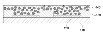
도 1을 참조하면, PCB 기판(110)의 표면에 형성된 금속 패드(120)는 고분자 소재를 사용한 솔더 마스크(130)에 의해 일정두께로 덮어져 있어 오목한 형상을 하고 있다. 이러한 금속 패드(120) 및 솔더 마스크(130)를 포함하는 PCB 기판(110) 전면에 일정한 두께의 SBM(Solder Bump Maker) 페이스트(140)를 도포한다.Referring to FIG. 1, a
SBM 페이스트(140)는 SBM 페이스트 100 중량% 기준으로 15 ~ 25 중량%의 고분자 수지, 1 ~ 10 중량%의 환원제 및 50 ~ 80 중량%의 솔더를 포함한다.The
고분자 수지는 온도의 증감에 따라 반응을 나타내지 않는 일원계 소재로서, DGEBA, TGDDM, TriTGDDM, 이소시아네이트(Isocyanate), 비스말레이미드(Bismaleimide), 에폭시 변성 실리콘 오일, 아민변성 실리콘 오일, 카복실 변성실리콘 오일 및 폴리올 등을 포함할 수 있다.The polymer resin is a one-component material which does not react with the increase or decrease of temperature, and is a material which can be used in the present invention as a base material, such as DGEBA, TGDDM, TriTGDDM, isocyanate, bismaleimide, epoxy- modified silicone oil, Polyols, and the like.
환원제는 글루타르산(Glutaric Acid), 말산(Malic Acid), 아젤라익산(Azelaic Acid), 아비에트산(Abietic Acid), 아디프산(Adipic Acid), 아스코르빈산(Ascorbic Acid), 아크릴산(Acrylic Acid) 및 시트르산(Citric Acid) 등을 포함할 수 있다.The reducing agent is selected from the group consisting of Glutaric Acid, Malic Acid, Azelaic Acid, Abietic Acid, Adipic Acid, Ascorbic Acid, Acrylic Acid, Acid) and citric acid (Citric Acid).
또한, 솔더의 입자 크기는 0.1um ~ 70um이고, 솔더는 Sn, Bi, Ag, Cu, In 및 Pb의 합금, 바람직하게는 60Sn/40Bi, 52In/48Sn, 97In/3Ag, 57Bi/42Sn/1Ag, 58Bi/42Sn, 52Bi/32Pb/16Sn 및 96.5Sn/3Ag/0.5Cu의 조성이 사용되며, 솔벤트와 같은 용제를 사용하지 않는다.In addition, the particle size of the solder is 0.1 um to 70 um, and the solder is an alloy of Sn, Bi, Ag, Cu, In and Pb, preferably 60Sn / 40Bi, 52In / 48Sn, 97In / 3Ag, 57Bi / 42Sn / A composition of 58Bi / 42Sn, 52Bi / 32Pb / 16Sn and 96.5Sn / 3Ag / 0.5Cu is used, and no solvent or solvent is used.
본 발명에서는 금속 패드(120)뿐만 아니라 솔더 마스크(130)를 포함한 PCB 기판(110) 전면에 SBM 페이스트(140)를 일정두께로 도포함으로써, 130um 피치 이하의 PCB 기판에서도 솔더 범프를 용이하게 형성할 수 있다.In the present invention, the SBM
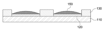
도 2를 참조하면, SBM 페이스트(140)를 SBM 페이스트(140)에 포함된 솔더의 녹는점보다 높은 온도로 가열한 후 냉각시킨다. 따라서, 솔더 입자들이 금속 패드(120) 위에서 젖음 특성을 나타내어 작은 부피의 솔더 범프(Low Volume Solder on Pad, 이하, 'LVSoP')(150)가 형성된다. 이때, SBM 페이스트(140)에 포함된 고분자 수지는 공정 이후에도 상온 상태에서 액체의 특성을 나타내고, 금속 패드(120)의 젖음 특성에 참여하지 않은 솔더 입자는 SBM 페이스트(140)의 고분자 수지 내에 갇혀있게 된다.Referring to FIG. 2, the
도 3을 참조하면, SBM 페이스트(140)의 잔여 고분자 수지와 잔여 솔더 입자를 솔벤트를 이용하여 세척한다.Referring to FIG. 3, the residual polymer resin and residual solder particles of the
최종적으로, LVSoP(150)의 높이는 솔더 마스크(130)의 높이와 비슷하다.
Finally, the height of the LVSoP 150 is similar to the height of the
도 4 내지 도 6은 본 발명의 다른 실시예에 따른 LVSoP가 형성된 PCB 기판에 반도체 소자의 플립 칩 본딩 방법을 설명하기 위한 공정 흐름도이다.FIGS. 4 to 6 are flowcharts illustrating a flip-chip bonding method of a semiconductor device on a PCB substrate on which LVSoP is formed according to another embodiment of the present invention.
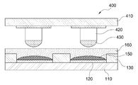
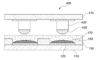
도 4를 참조하면, LVSoP(150)가 형성된 PCB 기판(110)에 플립 칩 본딩되는 반도체 소자(400)가 도시되어 있다. 반도체 소자(400)의 기판(410)에는 도출된 형상의 구리 필러(Cu Pillar)(420)가 형성되어 있고, 구리 필러(420)의 끝단에는 솔더 캡(Solder Cap) 또는 니켈 캡(Nikel Cap)(430)이 형성될 수 있다. 여기서, 솔더 캡 또는 니켈 캡(430)은 필요에 따라 생략될 수 있다.Referring to FIG. 4, there is shown a
도 5를 참조하면, LVSoP(150)가 형성된 PCB 기판(110)의 표면에 산화막 제거를 위한 플럭스(160)를 도포한다.Referring to FIG. 5, a
도 6을 참조하면, 열과 약간의 압력을 가하여 반도체 소자(400)를 플럭스(160)가 도포된 PCB 기판(110)에 플립 칩 본딩한 후, 잔류 플럭스를 제거한다. 이때, LVSoP(150)에 높은 압력을 가하여도 반도체 소자(400)와 PCB 기판(110) 사이에 일정한 거리가 유지됨으로써 솔더(152)가 금속 패드(120)를 벗어나 인접한 금속 패드가 전기적으로 연결되는 현상을 방지할 수 있다. 따라서, 본 발명에 따른 LVSoP(150)를 사용하는 경우 반도체 소자의 플립 칩 본딩시 압력 사용 여부에 상관없이 인접한 금속 패드 간의 전기적 연결을 완벽하게 방지할 수 있다.
Referring to FIG. 6, the
도 7 및 도 8은 본 발명의 또 다른 실시예에 따른 LVSoP가 형성된 PCB 기판에 반도체 소자의 플립 칩 본딩 방법을 설명하기 위한 공정 흐름도이다.7 and 8 are flowcharts for explaining a flip chip bonding method of a semiconductor device on a PCB substrate on which LVSoP is formed according to another embodiment of the present invention.
도 7을 참조하면, LVSoP(150)가 형성된 PCB 기판(110)의 표면에 산화막 제거 및 언더필 기능을 동시에 수행하는 플럭싱 언더필(170)을 도포한다. 여기서, 플럭싱 언더필(170)은 저융점 솔더를 포함하지 않는 열경화 혼합물이나 광경화 물질 등이 될 수 있다.Referring to FIG. 7, a
도 8을 참조하면, 열과 약간의 압력을 가하여 반도체 소자(400)를 플럭싱 언더필(170)이 도포된 PCB 기판(110)에 플립 칩 본딩한다. 여기서, 플럭싱 언더필(170)은 LVSoP(150)의 산화막을 제거하고, LVSoP(150)가 젖음 특성을 나타낸 이후에 경화되어 액체 상태에서 고체 상태로 변화된다.Referring to FIG. 8, the
따라서, 도 8에 도시된 바와 같이, LVSoP(150)가 형성된 PCB 기판(110)에 플럭싱 언더필(170)을 사용하여 플립 칩 본딩을 수행하는 경우 플럭싱 언더필(170)이 구리 필러(420) 및 솔더(152)를 감싸는 형상을 가짐으로써 매우 우수한 신뢰성을 기대할 수 있다.
8, when the flip chip bonding is performed using the
도 9는 70um의 직경 및 130um의 피치를 가지는 금속 패드와 약 10um의 두께를 가지는 솔더 마스크가 형성된 PCB 기판의 SEM 사진이다.9 is a SEM photograph of a PCB substrate having a metal pad having a diameter of 70 um and a pitch of 130 um and a solder mask having a thickness of about 10 um.
도 9에 도시된 바와 같이, PCB 기판의 금속 패드(120)는 오목한 원형 형상을 하고 있다.As shown in FIG. 9, the
이에, 도 1의 공정에 따라 PCB 기판 전면에 SBM 페이스트를 약 30um의 두께로 도포하고, 도 2의 공정에 따라 SBM 페이스트를 200도까지 승온시켜 약 10초간 유지한 후 상온으로 냉각시킨다. 이후에 도 3의 공정에 따라 아세톤과 물을 사용하여 초음파 세척기로 SBM 페이스트의 잔여 고분자 수지와 잔여 솔더 입자를 세척한다.1, the SBM paste is applied to the entire surface of the PCB substrate to a thickness of about 30 μm, the SBM paste is heated to 200 ° C. according to the process of FIG. 2, and then the substrate is kept at the room temperature for about 10 seconds. Thereafter, the residual polymer resin and the residual solder particles of the SBM paste are washed with an ultrasonic cleaner using acetone and water according to the process of FIG.
결과적으로, 도 10에 도시된 바와 같이, PCB 기판의 금속 패드 위에 LVSoP(150)가 형성된다.As a result, as shown in FIG. 10, the LVSoP 150 is formed on the metal pad of the PCB substrate.
도 11은 PCB 기판의 금속 패드를 기준면으로 하여 측정된 LVSoP의 높이를 나타낸 그래프로서, 약 3 ~ 4개의 LVSoP가 솔더 마스크보다 높고, 대부분의 LVSoP는 5 ~ 10um의 높이로 측정되었다.FIG. 11 is a graph showing the height of LVSoP measured with reference to a metal pad of a PCB substrate. As shown in FIG. 11, about 3 to 4 LVSoPs were higher than solder masks, and most LVSoPs were measured at 5 to 10 .mu.m height.
따라서, 도 10의 LVSoP가 형성된 PCB 기판에 코이닝 공정을 수행하여 도 12에서와 같이 솔더 마스크보다 높이가 높은 LVSoP(150a)를 평평하게 해줄 수도 있다.
Therefore, the LVSoP 150a having a height higher than the solder mask may be flattened as shown in FIG. 12 by performing a coining process on the PCB substrate having the LVSoP shown in FIG.
본 발명의 명세서에 개시된 실시예들은 본 발명을 한정하는 것이 아니다. 본 발명의 범위는 아래의 특허청구범위에 의해 해석되어야 하며, 그와 균등한 범위 내에 있는 모든 기술도 본 발명의 범위에 포함되는 것으로 해석해야 할 것이다.
The embodiments disclosed in the specification of the present invention do not limit the present invention. The scope of the present invention should be construed according to the following claims, and all the techniques within the scope of equivalents should be construed as being included in the scope of the present invention.
110: PCB 기판 120: 금속 패드
130: 솔더 마스크 140: SBM 페이스트
150: LVSoP110: PCB substrate 120: metal pad
130: Solder mask 140: SBM paste
150: LVSoP
Claims (12)
상기 SBM 페이스트를 상기 SBM 페이스트에 포함된 솔더의 녹는점보다 높은 온도로 가열한 후 냉각시켜 솔더 범프를 형성하는 단계; 및
상기 SBM 페이스트의 잔여 고분자 수지와 잔여 솔더 입자를 솔벤트를 사용하여 세척하는 단계;
를 포함하는 미세 피치 PCB 기판에 솔더 범프 형성 방법.
Applying a solder bump maker (SBM) paste having a predetermined thickness on the entire surface of the PCB including the metal pad and the solder mask;
Heating the SBM paste to a temperature higher than the melting point of the solder contained in the SBM paste and cooling the solder bump to form a solder bump; And
Washing the remaining polymer resin and residual solder particles of the SBM paste using a solvent;
Wherein the solder bump is formed on the substrate.
상기 SBM 페이스트의 솔더 입자들이 상기 금속 패드 위에서 젖음 특성을 나타내어 솔더 범프가 형성되는 것을 특징으로 하는 미세 피치 PCB 기판에 솔더 범프 형성 방법.
2. The method of claim 1, wherein in forming the solder bump,
Wherein the solder particles of the SBM paste exhibit a wetting property on the metal pad to form a solder bump.
상기 SBM 페이스트는 SBM 페이스트 100 중량% 기준으로 15 ~ 25 중량%의 고분자 수지, 1 ~ 10 중량%의 환원제 및 50 ~ 80 중량%의 솔더를 포함하는 것을 특징으로 하는 미세 피치 PCB 기판에 솔더 범프 형성 방법.
The method according to claim 1,
Wherein the SBM paste comprises 15 to 25% by weight of a polymer resin based on 100% by weight of the SBM paste, 1 to 10% by weight of a reducing agent, and 50 to 80% by weight of a solder. Way.
상기 고분자 수지는 DGEBA, TGDDM, TriTGDDM, 이소시아네이트(Isocyanate), 비스말레이미드(Bismaleimide), 에폭시 변성 실리콘 오일, 아민변성 실리콘 오일, 카복실 변성실리콘 오일 및 폴리올 중 적어도 하나를 포함하는 것을 특징으로 하는 미세 피치 PCB 기판에 솔더 범프 형성 방법.
The method of claim 3,
Wherein the polymer resin comprises at least one of DGEBA, TGDDM, TriTGDDM, isocyanate, bismaleimide, epoxy modified silicone oil, amine modified silicone oil, carboxyl modified silicone oil and polyol. A method of forming a solder bump on a PCB substrate.
상기 환원제는 글루타르산(Glutaric Acid), 말산(Malic Acid), 아젤라익산(Azelaic Acid), 아비에트산(Abietic Acid), 아디프산(Adipic Acid), 아스코르빈산(Ascorbic Acid), 아크릴산(Acrylic Acid) 및 시트르산(Citric Acid) 중 적어도 하나를 포함하는 것을 특징으로 하는 미세 피치 PCB 기판에 솔더 범프 형성 방법.
The method of claim 3,
The reducing agent may be selected from the group consisting of Glutaric Acid, Malic Acid, Azelaic Acid, Abietic Acid, Adipic Acid, Ascorbic Acid, Wherein the solder bump is formed of at least one selected from the group consisting of Acrylic Acid and Citric Acid.
상기 솔더의 입자 크기는 0.1um ~ 70um인 것을 특징으로 하는 미세 피치 PCB 기판에 솔더 범프 형성 방법.
The method of claim 3,
Wherein the particle size of the solder is from 0.1 um to 70 um. ≪ RTI ID = 0.0 > 11. < / RTI >
상기 솔더는 Sn, Bi, Ag, Cu, In 및 Pb 중 적어도 하나를 포함하는 것을 특징으로 하는 미세 피치 PCB 기판에 솔더 범프 형성 방법.
The method of claim 3,
Wherein the solder comprises at least one of Sn, Bi, Ag, Cu, In, and Pb.
상기 솔더 범프가 형성된 PCB 기판에 코이닝 공정을 수행하는 단계;
를 더 포함하는 것을 특징으로 하는 미세 피치 PCB 기판에 솔더 범프 형성 방법.
The method according to claim 1,
Performing a coining process on the PCB substrate on which the solder bumps are formed;
Further comprising the steps of: forming a solder bump on the substrate;
상기 SBM 페이스트를 상기 SBM 페이스트에 포함된 솔더의 녹는점보다 높은 온도로 가열한 후 냉각시켜 솔더 범프를 형성하는 단계;
상기 SBM 페이스트의 잔여 고분자 수지와 잔여 솔더 입자를 솔벤트를 사용하여 세척하는 단계;
상기 솔더 범프가 형성된 PCB 기판 전면에 산화막 제거를 위한 플럭스를 도포하는 단계;
상기 플럭스가 도포된 PCB 기판에 구리 필러가 형성된 반도체 소자를 플립 칩 본딩하는 단계; 및
잔류 플럭스를 제거하는 단계;
를 포함하는 반도체 소자의 플립 칩 본딩 방법.
Applying a solder bump maker (SBM) paste having a predetermined thickness on the entire surface of the PCB including the metal pad and the solder mask;
Heating the SBM paste to a temperature higher than the melting point of the solder contained in the SBM paste and cooling the solder bump to form a solder bump;
Washing the remaining polymer resin and residual solder particles of the SBM paste using a solvent;
Applying a flux for removing an oxide film to the entire surface of the PCB having the solder bumps formed therein;
Flip-chip bonding a semiconductor device having a copper filler formed on a PCB substrate coated with the flux; And
Removing the residual flux;
Wherein the flip chip bonding method comprises the steps of:
상기 구리 필러의 끝단에 솔더 캡 또는 니켈 캡이 형성되어 있는 것을 특징으로 하는 반도체 소자의 플립 칩 본딩 방법.
10. The method of claim 9,
And a solder cap or a nickel cap is formed on an end of the copper filler.
상기 SBM 페이스트를 상기 SBM 페이스트에 포함된 솔더의 녹는점보다 높은 온도로 가열한 후 냉각시켜 솔더 범프를 형성하는 단계;
상기 SBM 페이스트의 잔여 고분자 수지와 잔여 솔더 입자를 솔벤트를 사용하여 세척하는 단계;
상기 솔더 범프가 형성된 PCB 기판 전면에 산화막 제거 및 언더필 기능을 수행하는 플럭싱 언더필을 도포하는 단계; 및
상기 플럭싱 언더필이 도포된 PCB 기판에 구리 필러가 형성된 반도체 소자를 플립 칩 본딩하는 단계;
를 포함하는 반도체 소자의 플립 칩 본딩 방법.
Applying a solder bump maker (SBM) paste having a predetermined thickness on the entire surface of the PCB including the metal pad and the solder mask;
Heating the SBM paste to a temperature higher than the melting point of the solder contained in the SBM paste and cooling the solder bump to form a solder bump;
Washing the remaining polymer resin and residual solder particles of the SBM paste using a solvent;
Applying a fluxing underfill to the entire surface of the PCB on which the solder bumps are formed to perform an oxide film removal and an underfill function; And
Flip chip bonding a semiconductor device having a copper filler formed on a PCB substrate coated with the fluxing underfill;
Wherein the flip chip bonding method comprises the steps of:
상기 구리 필러의 끝단에 솔더 캡 또는 니켈 캡이 형성되어 있는 것을 특징으로 하는 반도체 소자의 플립 칩 본딩 방법.
12. The method of claim 11,
And a solder cap or a nickel cap is formed on an end of the copper filler.
Priority Applications (2)
| Application Number | Priority Date | Filing Date | Title |
|---|---|---|---|
| KR1020120063792A KR101940237B1 (en) | 2012-06-14 | 2012-06-14 | Method for Manufacturing Solder on Pad on Fine Pitch PCB Substrate and Flip Chip Bonding Method of Semiconductor Using The Same |
| US13/760,350 US8794502B2 (en) | 2012-06-14 | 2013-02-06 | Method of forming solder on pad on fine pitch PCB and method of flip chip bonding semiconductor using the same |
Applications Claiming Priority (1)
| Application Number | Priority Date | Filing Date | Title |
|---|---|---|---|
| KR1020120063792A KR101940237B1 (en) | 2012-06-14 | 2012-06-14 | Method for Manufacturing Solder on Pad on Fine Pitch PCB Substrate and Flip Chip Bonding Method of Semiconductor Using The Same |
Publications (2)
| Publication Number | Publication Date |
|---|---|
| KR20130140407A true KR20130140407A (en) | 2013-12-24 |
| KR101940237B1 KR101940237B1 (en) | 2019-01-18 |
Family
ID=49754972
Family Applications (1)
| Application Number | Title | Priority Date | Filing Date |
|---|---|---|---|
| KR1020120063792A Active KR101940237B1 (en) | 2012-06-14 | 2012-06-14 | Method for Manufacturing Solder on Pad on Fine Pitch PCB Substrate and Flip Chip Bonding Method of Semiconductor Using The Same |
Country Status (2)
| Country | Link |
|---|---|
| US (1) | US8794502B2 (en) |
| KR (1) | KR101940237B1 (en) |
Cited By (3)
| Publication number | Priority date | Publication date | Assignee | Title |
|---|---|---|---|---|
| KR20210076493A (en) * | 2019-12-16 | 2021-06-24 | 주식회사 노피온 | Cluster type anisotropic conductive adhesive film containing thermoplastic resin, a method of forming solder bumps and a method of manufacturing a bonded structure using the same |
| KR20210076511A (en) * | 2019-12-16 | 2021-06-24 | 주식회사 노피온 | Anisotropic conductive adhesive containing polyurethane resin which is a thermoplastic resin, a method of forming solder bumps and a method of manufacturing a bonded structure using the same |
| KR20210076619A (en) * | 2019-12-16 | 2021-06-24 | 주식회사 노피온 | Anisotropic conductive adhesive containing a polysiloxane resin which is a thermoplastic resin, a method of forming solder bumps and a method of manufacturing a bonded structure using the same |
Families Citing this family (7)
| Publication number | Priority date | Publication date | Assignee | Title |
|---|---|---|---|---|
| KR102060831B1 (en) * | 2013-02-27 | 2019-12-30 | 삼성전자주식회사 | Flip chip packaging method, flux head using the same and flux head manufacturing method thereof |
| US10160066B2 (en) * | 2016-11-01 | 2018-12-25 | GM Global Technology Operations LLC | Methods and systems for reinforced adhesive bonding using solder elements and flux |
| US10741482B2 (en) | 2017-12-29 | 2020-08-11 | Advanced Semiconductor Engineering, Inc. | Semiconductor device package |
| CN110557937B (en) | 2018-05-31 | 2021-08-06 | 铟泰公司 | Flux that effectively suppresses non-wetting openings in BGA assemblies |
| US11488841B2 (en) * | 2019-02-20 | 2022-11-01 | Electronics And Telecommunications Research Institute | Method for manufacturing semiconductor package |
| US11688706B2 (en) * | 2020-09-15 | 2023-06-27 | Micron Technology, Inc. | Semiconductor device assembly with embossed solder mask having non-planar features and associated methods and systems |
| KR102272987B1 (en) * | 2021-01-27 | 2021-07-05 | 주식회사 프로이천 | Bump Type Probe Card |
Citations (4)
| Publication number | Priority date | Publication date | Assignee | Title |
|---|---|---|---|---|
| JPH10107415A (en) * | 1996-10-02 | 1998-04-24 | Furukawa Electric Co Ltd:The | Solder supply method |
| JP2007227788A (en) * | 2006-02-24 | 2007-09-06 | Kyocer Slc Technologies Corp | Wiring board fabrication method, and soldering paste |
| KR20090011198A (en) * | 2007-07-25 | 2009-02-02 | 앰코 테크놀로지 코리아 주식회사 | Semiconductor package and manufacturing method thereof |
| KR20100007690A (en) * | 2008-07-10 | 2010-01-22 | 한국전자통신연구원 | Composition, and methods of forming solder bump and flip chip using the same |
Family Cites Families (46)
| Publication number | Priority date | Publication date | Assignee | Title |
|---|---|---|---|---|
| USRE32309E (en) * | 1983-10-31 | 1986-12-16 | Scm Corporation | Fusible powdered metal paste |
| US4619715A (en) * | 1984-09-11 | 1986-10-28 | Scm Corporation | Fusible powdered metal paste |
| JPH03165999A (en) * | 1989-11-24 | 1991-07-17 | Nippondenso Co Ltd | Water soluble flux for soldering |
| JPH06125169A (en) * | 1992-10-13 | 1994-05-06 | Fujitsu Ltd | Pre-soldering method |
| US5478700A (en) * | 1993-12-21 | 1995-12-26 | International Business Machines Corporation | Method for applying bonding agents to pad and/or interconnection sites in the manufacture of electrical circuits using a bonding agent injection head |
| GB9410128D0 (en) * | 1994-05-20 | 1994-07-06 | Burton Chambers Roderick L | Post arrangement |
| JP3224185B2 (en) * | 1994-09-29 | 2001-10-29 | 富士通株式会社 | Solder alloy, solder powder, solder paste, printed wiring board, electronic component, soldering method and soldering apparatus |
| US5868302A (en) * | 1995-09-06 | 1999-02-09 | Matsushita Electric Industrial Co., Ltd. | Method and apparatus for mounting electronic component |
| DE69737281T2 (en) * | 1996-12-10 | 2007-12-20 | Matsushita Electric Industrial Co., Ltd., Kadoma | Apparatus and method for printing solder paste |
| US7654432B2 (en) | 1997-05-27 | 2010-02-02 | Wstp, Llc | Forming solder balls on substrates |
| US6609652B2 (en) * | 1997-05-27 | 2003-08-26 | Spheretek, Llc | Ball bumping substrates, particuarly wafers |
| JP2000062136A (en) * | 1998-08-21 | 2000-02-29 | Matsushita Electric Ind Co Ltd | Printing method of metal paste |
| US6173887B1 (en) * | 1999-06-24 | 2001-01-16 | International Business Machines Corporation | Method of making electrically conductive contacts on substrates |
| JP3831179B2 (en) * | 1999-06-29 | 2006-10-11 | 株式会社東芝 | Semiconductor device manufacturing method and pattern forming method |
| JP3403677B2 (en) * | 1999-09-06 | 2003-05-06 | マイクロ・テック株式会社 | Solder ball forming method |
| JP2002076589A (en) * | 2000-08-31 | 2002-03-15 | Hitachi Ltd | Electronic device and manufacturing method thereof |
| US6845901B2 (en) * | 2002-08-22 | 2005-01-25 | Micron Technology, Inc. | Apparatus and method for depositing and reflowing solder paste on a microelectronic workpiece |
| JP2004174538A (en) * | 2002-11-26 | 2004-06-24 | Ricoh Co Ltd | Method for producing solder alloy material, and ink composition containing solder alloy |
| US7059512B2 (en) * | 2002-11-06 | 2006-06-13 | Ricoh Company, Ltd. | Solder alloy material layer composition, electroconductive and adhesive composition, flux material layer composition, solder ball transferring sheet, bump and bump forming process, and semiconductor device |
| US7043830B2 (en) * | 2003-02-20 | 2006-05-16 | Micron Technology, Inc. | Method of forming conductive bumps |
| US20040219774A1 (en) * | 2003-05-02 | 2004-11-04 | Yu-Nung Shen | Method for forming conductive bump and device formed with such a conductive bump |
| JP2005026579A (en) * | 2003-07-04 | 2005-01-27 | Fujitsu Ltd | Mounting method of electronic component with solder bump and flux fill used therefor |
| US20050058771A1 (en) * | 2003-09-16 | 2005-03-17 | International Business Machines Corporation | Rolling contact screening method and apparatus |
| JP2005183904A (en) * | 2003-12-22 | 2005-07-07 | Rohm & Haas Electronic Materials Llc | Method for forming solder region on electronic part and electronic part with solder region |
| US7213739B2 (en) * | 2004-04-02 | 2007-05-08 | Fry's Metals, Inc. | Underfill fluxing curative |
| JP3964911B2 (en) | 2004-09-03 | 2007-08-22 | 松下電器産業株式会社 | Manufacturing method of substrate with bumps |
| JP4740865B2 (en) * | 2004-09-24 | 2011-08-03 | 学校法人日本大学 | Manufacturing method of ceramic electronic component |
| JP4512497B2 (en) * | 2005-01-31 | 2010-07-28 | イビデン株式会社 | Capacitor built-in package substrate and manufacturing method thereof |
| CN100511618C (en) * | 2005-03-09 | 2009-07-08 | 松下电器产业株式会社 | Metal particle dispersion composition and method using the same |
| CN100495675C (en) * | 2005-03-17 | 2009-06-03 | 松下电器产业株式会社 | Assembly including semiconductor chip and method of manufacturing the same |
| EP1865549A4 (en) * | 2005-03-29 | 2012-07-11 | Panasonic Corp | RETURN CHIP MOUNTING METHOD AND DAMPER FORMING METHOD |
| KR101175482B1 (en) * | 2005-04-06 | 2012-08-20 | 파나소닉 주식회사 | flip chip mounting method and bump forming method |
| EP1996002B1 (en) * | 2006-03-16 | 2017-07-05 | Panasonic Intellectual Property Management Co., Ltd. | Bump forming method and bump forming apparatus |
| KR100765146B1 (en) | 2006-06-15 | 2007-10-12 | 배상준 | Solder Paste and Solder Bump Forming Method Using the Same |
| US20080003804A1 (en) * | 2006-06-29 | 2008-01-03 | Ravi Nalla | Method of providing solder bumps of mixed sizes on a substrate using solder transfer in two stages |
| US7906424B2 (en) * | 2007-08-01 | 2011-03-15 | Advanced Micro Devices, Inc. | Conductor bump method and apparatus |
| US20090057378A1 (en) * | 2007-08-27 | 2009-03-05 | Chi-Won Hwang | In-situ chip attachment using self-organizing solder |
| JP2009220493A (en) * | 2008-03-18 | 2009-10-01 | Nec Electronics Corp | Metal paste printing method and metal mask |
| US20100029074A1 (en) | 2008-05-28 | 2010-02-04 | Mackay John | Maskless Process for Solder Bump Production |
| US7867842B2 (en) * | 2008-07-29 | 2011-01-11 | International Business Machines Corporation | Method and apparatus for forming planar alloy deposits on a substrate |
| KR20100060968A (en) * | 2008-11-28 | 2010-06-07 | 삼성전기주식회사 | A substrate having a metal post and a fabricating method of the same |
| KR20110036450A (en) * | 2009-10-01 | 2011-04-07 | 삼성전기주식회사 | Method for manufacturing a flip chip substrate and a flip chip substrate manufactured using the same |
| KR101234597B1 (en) * | 2009-10-15 | 2013-02-22 | 한국전자통신연구원 | method for bonding flip chip and structure at the same |
| KR101061048B1 (en) * | 2010-02-17 | 2011-09-01 | (주)덕산테코피아 | Solder Ink and Electronic Device Package Using the Same |
| US8921221B2 (en) * | 2011-06-20 | 2014-12-30 | International Business Machines Corporation | IMS (injection molded solder) with two resist layers forming solder bumps on substrates |
| JP2014004819A (en) * | 2012-05-28 | 2014-01-16 | Hitachi High-Technologies Corp | Pattern forming method and forming apparatus thereof |
-
2012
- 2012-06-14 KR KR1020120063792A patent/KR101940237B1/en active Active
-
2013
- 2013-02-06 US US13/760,350 patent/US8794502B2/en active Active
Patent Citations (4)
| Publication number | Priority date | Publication date | Assignee | Title |
|---|---|---|---|---|
| JPH10107415A (en) * | 1996-10-02 | 1998-04-24 | Furukawa Electric Co Ltd:The | Solder supply method |
| JP2007227788A (en) * | 2006-02-24 | 2007-09-06 | Kyocer Slc Technologies Corp | Wiring board fabrication method, and soldering paste |
| KR20090011198A (en) * | 2007-07-25 | 2009-02-02 | 앰코 테크놀로지 코리아 주식회사 | Semiconductor package and manufacturing method thereof |
| KR20100007690A (en) * | 2008-07-10 | 2010-01-22 | 한국전자통신연구원 | Composition, and methods of forming solder bump and flip chip using the same |
Cited By (3)
| Publication number | Priority date | Publication date | Assignee | Title |
|---|---|---|---|---|
| KR20210076493A (en) * | 2019-12-16 | 2021-06-24 | 주식회사 노피온 | Cluster type anisotropic conductive adhesive film containing thermoplastic resin, a method of forming solder bumps and a method of manufacturing a bonded structure using the same |
| KR20210076511A (en) * | 2019-12-16 | 2021-06-24 | 주식회사 노피온 | Anisotropic conductive adhesive containing polyurethane resin which is a thermoplastic resin, a method of forming solder bumps and a method of manufacturing a bonded structure using the same |
| KR20210076619A (en) * | 2019-12-16 | 2021-06-24 | 주식회사 노피온 | Anisotropic conductive adhesive containing a polysiloxane resin which is a thermoplastic resin, a method of forming solder bumps and a method of manufacturing a bonded structure using the same |
Also Published As
| Publication number | Publication date |
|---|---|
| KR101940237B1 (en) | 2019-01-18 |
| US20130334291A1 (en) | 2013-12-19 |
| US8794502B2 (en) | 2014-08-05 |
Similar Documents
| Publication | Publication Date | Title |
|---|---|---|
| KR101940237B1 (en) | Method for Manufacturing Solder on Pad on Fine Pitch PCB Substrate and Flip Chip Bonding Method of Semiconductor Using The Same | |
| JP2807940B2 (en) | Adhesive having flux agent and metal particles | |
| CN101904230B (en) | The methods of fluxless micro-piercing of solder ball and the device of gained | |
| EP2427036B1 (en) | Process for production of circuit board | |
| TWI612591B (en) | Reflow film, solder bump forming method, solder bonding forming method, and semiconductor device | |
| JP2009158593A (en) | Bump structure and manufacturing method thereof | |
| US9978709B2 (en) | Solder bump stretching method for forming a solder bump joint in a device | |
| WO2014104218A1 (en) | Method for manufacturing circuit board to which electronic component is joined | |
| JP4729963B2 (en) | PROJECT ELECTRODE FOR CONNECTING ELECTRONIC COMPONENT, ELECTRONIC COMPONENT MOUNTING BODY USING SAME, AND METHOD FOR PRODUCING THEM | |
| JP4115306B2 (en) | Manufacturing method of semiconductor device | |
| KR102006637B1 (en) | Method Of Forming Bump And Semiconductor device including The Same | |
| KR101988890B1 (en) | method for manufacturing solder on pad and flip chip bonding method used the same | |
| JP2010157693A (en) | Semiconductor package substrate with metal bumps | |
| JP5560713B2 (en) | Electronic component mounting method, etc. | |
| JP2009021465A (en) | Semiconductor device mounting structure, method for manufacturing the same, and method for peeling semiconductor device | |
| CN103000609A (en) | Salient point preparing material and salient point preparing method | |
| JP2006100457A (en) | Electronic device and manufacturing method thereof | |
| JP4453919B2 (en) | Manufacturing method of electronic component with bump electrode | |
| TWI878402B (en) | Connecting structure and method for manufacturing the connecting structure | |
| JP6136411B2 (en) | Electronic component joining method and electronic apparatus | |
| JP2006100844A (en) | Electronic components with bump electrodes | |
| JP2002171055A (en) | Electronic circuit board, electronic component, electronic circuit device, and manufacturing method thereof | |
| JP6186884B2 (en) | Electrode, electronic component, electronic apparatus, and electrode joining method | |
| KR20120041430A (en) | Method for manufacturing a flip-chip solder-on-pad | |
| JP2014090216A (en) | Bump structure and method of manufacturing the same |
Legal Events
| Date | Code | Title | Description |
|---|---|---|---|
| PA0109 | Patent application |
St.27 status event code: A-0-1-A10-A12-nap-PA0109 |
|
| R17-X000 | Change to representative recorded |
St.27 status event code: A-3-3-R10-R17-oth-X000 |
|
| PG1501 | Laying open of application |
St.27 status event code: A-1-1-Q10-Q12-nap-PG1501 |
|
| PN2301 | Change of applicant |
St.27 status event code: A-3-3-R10-R13-asn-PN2301 St.27 status event code: A-3-3-R10-R11-asn-PN2301 |
|
| R17-X000 | Change to representative recorded |
St.27 status event code: A-3-3-R10-R17-oth-X000 |
|
| A201 | Request for examination | ||
| PA0201 | Request for examination |
St.27 status event code: A-1-2-D10-D11-exm-PA0201 |
|
| D13-X000 | Search requested |
St.27 status event code: A-1-2-D10-D13-srh-X000 |
|
| D14-X000 | Search report completed |
St.27 status event code: A-1-2-D10-D14-srh-X000 |
|
| E902 | Notification of reason for refusal | ||
| PE0902 | Notice of grounds for rejection |
St.27 status event code: A-1-2-D10-D21-exm-PE0902 |
|
| P11-X000 | Amendment of application requested |
St.27 status event code: A-2-2-P10-P11-nap-X000 |
|
| P13-X000 | Application amended |
St.27 status event code: A-2-2-P10-P13-nap-X000 |
|
| E90F | Notification of reason for final refusal | ||
| PE0902 | Notice of grounds for rejection |
St.27 status event code: A-1-2-D10-D21-exm-PE0902 |
|
| P11-X000 | Amendment of application requested |
St.27 status event code: A-2-2-P10-P11-nap-X000 |
|
| P13-X000 | Application amended |
St.27 status event code: A-2-2-P10-P13-nap-X000 |
|
| E701 | Decision to grant or registration of patent right | ||
| PE0701 | Decision of registration |
St.27 status event code: A-1-2-D10-D22-exm-PE0701 |
|
| GRNT | Written decision to grant | ||
| PR0701 | Registration of establishment |
St.27 status event code: A-2-4-F10-F11-exm-PR0701 |
|
| PR1002 | Payment of registration fee |
St.27 status event code: A-2-2-U10-U11-oth-PR1002 Fee payment year number: 1 |
|
| PG1601 | Publication of registration |
St.27 status event code: A-4-4-Q10-Q13-nap-PG1601 |
|
| PR1001 | Payment of annual fee |
St.27 status event code: A-4-4-U10-U11-oth-PR1001 Fee payment year number: 4 |
|
| PR1001 | Payment of annual fee |
St.27 status event code: A-4-4-U10-U11-oth-PR1001 Fee payment year number: 5 |
|
| PR1001 | Payment of annual fee |
St.27 status event code: A-4-4-U10-U11-oth-PR1001 Fee payment year number: 6 |
|
| PR1001 | Payment of annual fee |
St.27 status event code: A-4-4-U10-U11-oth-PR1001 Fee payment year number: 7 |
|
| P22-X000 | Classification modified |
St.27 status event code: A-4-4-P10-P22-nap-X000 |