JP4512497B2 - Capacitor built-in package substrate and manufacturing method thereof - Google Patents
Capacitor built-in package substrate and manufacturing method thereof Download PDFInfo
- Publication number
- JP4512497B2 JP4512497B2 JP2005022992A JP2005022992A JP4512497B2 JP 4512497 B2 JP4512497 B2 JP 4512497B2 JP 2005022992 A JP2005022992 A JP 2005022992A JP 2005022992 A JP2005022992 A JP 2005022992A JP 4512497 B2 JP4512497 B2 JP 4512497B2
- Authority
- JP
- Japan
- Prior art keywords
- thin film
- electrode
- film small
- electrodes
- capacitor
- Prior art date
- Legal status (The legal status is an assumption and is not a legal conclusion. Google has not performed a legal analysis and makes no representation as to the accuracy of the status listed.)
- Active
Links
- 239000003990 capacitor Substances 0.000 title claims description 138
- 239000000758 substrate Substances 0.000 title claims description 106
- 238000004519 manufacturing process Methods 0.000 title claims description 31
- 239000010409 thin film Substances 0.000 claims description 350
- 239000004020 conductor Substances 0.000 claims description 55
- 238000000034 method Methods 0.000 claims description 32
- 239000004065 semiconductor Substances 0.000 claims description 27
- RTAQQCXQSZGOHL-UHFFFAOYSA-N Titanium Chemical compound [Ti] RTAQQCXQSZGOHL-UHFFFAOYSA-N 0.000 claims description 15
- 239000007787 solid Substances 0.000 claims description 15
- 239000003989 dielectric material Substances 0.000 claims description 13
- 238000007689 inspection Methods 0.000 claims description 13
- 229910052751 metal Inorganic materials 0.000 claims description 12
- 239000002184 metal Substances 0.000 claims description 12
- 238000010030 laminating Methods 0.000 claims description 9
- 229910052451 lead zirconate titanate Inorganic materials 0.000 claims description 8
- JRPBQTZRNDNNOP-UHFFFAOYSA-N barium titanate Chemical compound [Ba+2].[Ba+2].[O-][Ti]([O-])([O-])[O-] JRPBQTZRNDNNOP-UHFFFAOYSA-N 0.000 claims description 7
- 229910002113 barium titanate Inorganic materials 0.000 claims description 7
- 238000010304 firing Methods 0.000 claims description 6
- 238000005520 cutting process Methods 0.000 claims description 4
- 239000011888 foil Substances 0.000 claims description 4
- 229910044991 metal oxide Inorganic materials 0.000 claims description 4
- 150000004706 metal oxides Chemical class 0.000 claims description 4
- FFQALBCXGPYQGT-UHFFFAOYSA-N 2,4-difluoro-5-(trifluoromethyl)aniline Chemical compound NC1=CC(C(F)(F)F)=C(F)C=C1F FFQALBCXGPYQGT-UHFFFAOYSA-N 0.000 claims description 3
- DJOYTAUERRJRAT-UHFFFAOYSA-N 2-(n-methyl-4-nitroanilino)acetonitrile Chemical compound N#CCN(C)C1=CC=C([N+]([O-])=O)C=C1 DJOYTAUERRJRAT-UHFFFAOYSA-N 0.000 claims description 3
- 229910052746 lanthanum Inorganic materials 0.000 claims description 3
- FZLIPJUXYLNCLC-UHFFFAOYSA-N lanthanum atom Chemical compound [La] FZLIPJUXYLNCLC-UHFFFAOYSA-N 0.000 claims description 3
- HFGPZNIAWCZYJU-UHFFFAOYSA-N lead zirconate titanate Chemical compound [O-2].[O-2].[O-2].[O-2].[O-2].[Ti+4].[Zr+4].[Pb+2] HFGPZNIAWCZYJU-UHFFFAOYSA-N 0.000 claims description 3
- 229910052758 niobium Inorganic materials 0.000 claims description 3
- 239000010955 niobium Substances 0.000 claims description 3
- GUCVJGMIXFAOAE-UHFFFAOYSA-N niobium atom Chemical compound [Nb] GUCVJGMIXFAOAE-UHFFFAOYSA-N 0.000 claims description 3
- BPUBBGLMJRNUCC-UHFFFAOYSA-N oxygen(2-);tantalum(5+) Chemical compound [O-2].[O-2].[O-2].[O-2].[O-2].[Ta+5].[Ta+5] BPUBBGLMJRNUCC-UHFFFAOYSA-N 0.000 claims description 3
- VEALVRVVWBQVSL-UHFFFAOYSA-N strontium titanate Chemical compound [Sr+2].[O-][Ti]([O-])=O VEALVRVVWBQVSL-UHFFFAOYSA-N 0.000 claims description 3
- 229910001936 tantalum oxide Inorganic materials 0.000 claims description 3
- 239000002994 raw material Substances 0.000 claims description 2
- 239000010410 layer Substances 0.000 description 193
- RYGMFSIKBFXOCR-UHFFFAOYSA-N Copper Chemical compound [Cu] RYGMFSIKBFXOCR-UHFFFAOYSA-N 0.000 description 75
- 229910052802 copper Inorganic materials 0.000 description 57
- 239000010949 copper Substances 0.000 description 57
- 229920005989 resin Polymers 0.000 description 41
- 239000011347 resin Substances 0.000 description 41
- 229910000679 solder Inorganic materials 0.000 description 26
- 239000011889 copper foil Substances 0.000 description 18
- 238000005530 etching Methods 0.000 description 14
- MCMNRKCIXSYSNV-UHFFFAOYSA-N Zirconium dioxide Chemical compound O=[Zr]=O MCMNRKCIXSYSNV-UHFFFAOYSA-N 0.000 description 8
- 238000007747 plating Methods 0.000 description 8
- 229920001721 polyimide Polymers 0.000 description 7
- 239000009719 polyimide resin Substances 0.000 description 7
- PXHVJJICTQNCMI-UHFFFAOYSA-N Nickel Chemical compound [Ni] PXHVJJICTQNCMI-UHFFFAOYSA-N 0.000 description 6
- 239000000919 ceramic Substances 0.000 description 6
- ORTQZVOHEJQUHG-UHFFFAOYSA-L copper(II) chloride Chemical compound Cl[Cu]Cl ORTQZVOHEJQUHG-UHFFFAOYSA-L 0.000 description 6
- 230000002542 deteriorative effect Effects 0.000 description 6
- 239000011229 interlayer Substances 0.000 description 6
- BASFCYQUMIYNBI-UHFFFAOYSA-N platinum Chemical compound [Pt] BASFCYQUMIYNBI-UHFFFAOYSA-N 0.000 description 6
- 238000009713 electroplating Methods 0.000 description 5
- 239000003822 epoxy resin Substances 0.000 description 5
- 239000000463 material Substances 0.000 description 5
- 230000000149 penetrating effect Effects 0.000 description 5
- 229920000647 polyepoxide Polymers 0.000 description 5
- IJGRMHOSHXDMSA-UHFFFAOYSA-N Atomic nitrogen Chemical compound N#N IJGRMHOSHXDMSA-UHFFFAOYSA-N 0.000 description 4
- CURLTUGMZLYLDI-UHFFFAOYSA-N Carbon dioxide Chemical compound O=C=O CURLTUGMZLYLDI-UHFFFAOYSA-N 0.000 description 4
- VYPSYNLAJGMNEJ-UHFFFAOYSA-N Silicium dioxide Chemical compound O=[Si]=O VYPSYNLAJGMNEJ-UHFFFAOYSA-N 0.000 description 4
- PNEYBMLMFCGWSK-UHFFFAOYSA-N aluminium oxide Inorganic materials [O-2].[O-2].[O-2].[Al+3].[Al+3] PNEYBMLMFCGWSK-UHFFFAOYSA-N 0.000 description 4
- 150000001916 cyano esters Chemical class 0.000 description 4
- 239000010408 film Substances 0.000 description 4
- 238000009413 insulation Methods 0.000 description 4
- 229920001955 polyphenylene ether Polymers 0.000 description 4
- 229920001187 thermosetting polymer Polymers 0.000 description 4
- 238000001771 vacuum deposition Methods 0.000 description 4
- JOYRKODLDBILNP-UHFFFAOYSA-N Ethyl urethane Chemical compound CCOC(N)=O JOYRKODLDBILNP-UHFFFAOYSA-N 0.000 description 3
- 241001424392 Lucia limbaria Species 0.000 description 3
- 239000000654 additive Substances 0.000 description 3
- 229960003280 cupric chloride Drugs 0.000 description 3
- 238000001035 drying Methods 0.000 description 3
- 230000000694 effects Effects 0.000 description 3
- 239000000945 filler Substances 0.000 description 3
- PCHJSUWPFVWCPO-UHFFFAOYSA-N gold Chemical compound [Au] PCHJSUWPFVWCPO-UHFFFAOYSA-N 0.000 description 3
- 229910052737 gold Inorganic materials 0.000 description 3
- 239000010931 gold Substances 0.000 description 3
- 150000003949 imides Chemical class 0.000 description 3
- 239000012784 inorganic fiber Substances 0.000 description 3
- 229910052759 nickel Inorganic materials 0.000 description 3
- 229910052697 platinum Inorganic materials 0.000 description 3
- 229920005672 polyolefin resin Polymers 0.000 description 3
- 229920002050 silicone resin Polymers 0.000 description 3
- 238000004544 sputter deposition Methods 0.000 description 3
- 229920005992 thermoplastic resin Polymers 0.000 description 3
- 239000010936 titanium Substances 0.000 description 3
- 229910052719 titanium Inorganic materials 0.000 description 3
- 229910052720 vanadium Inorganic materials 0.000 description 3
- UFWIBTONFRDIAS-UHFFFAOYSA-N Naphthalene Chemical compound C1=CC=CC2=CC=CC=C21 UFWIBTONFRDIAS-UHFFFAOYSA-N 0.000 description 2
- KDLHZDBZIXYQEI-UHFFFAOYSA-N Palladium Chemical compound [Pd] KDLHZDBZIXYQEI-UHFFFAOYSA-N 0.000 description 2
- 229910002367 SrTiO Inorganic materials 0.000 description 2
- ATJFFYVFTNAWJD-UHFFFAOYSA-N Tin Chemical compound [Sn] ATJFFYVFTNAWJD-UHFFFAOYSA-N 0.000 description 2
- 230000000996 additive effect Effects 0.000 description 2
- 229910002092 carbon dioxide Inorganic materials 0.000 description 2
- 239000001569 carbon dioxide Substances 0.000 description 2
- 239000003054 catalyst Substances 0.000 description 2
- 238000010586 diagram Methods 0.000 description 2
- DOIRQSBPFJWKBE-UHFFFAOYSA-N dibutyl phthalate Chemical compound CCCCOC(=O)C1=CC=CC=C1C(=O)OCCCC DOIRQSBPFJWKBE-UHFFFAOYSA-N 0.000 description 2
- 239000013013 elastic material Substances 0.000 description 2
- 229920001971 elastomer Polymers 0.000 description 2
- LZCLXQDLBQLTDK-UHFFFAOYSA-N ethyl 2-hydroxypropanoate Chemical compound CCOC(=O)C(C)O LZCLXQDLBQLTDK-UHFFFAOYSA-N 0.000 description 2
- 238000011049 filling Methods 0.000 description 2
- 239000000203 mixture Substances 0.000 description 2
- 229910052757 nitrogen Inorganic materials 0.000 description 2
- 239000000843 powder Substances 0.000 description 2
- 239000002243 precursor Substances 0.000 description 2
- 239000000047 product Substances 0.000 description 2
- 238000007788 roughening Methods 0.000 description 2
- 239000000377 silicon dioxide Substances 0.000 description 2
- 229920002379 silicone rubber Polymers 0.000 description 2
- 238000005476 soldering Methods 0.000 description 2
- 238000004528 spin coating Methods 0.000 description 2
- 239000000126 substance Substances 0.000 description 2
- XLYOFNOQVPJJNP-UHFFFAOYSA-N water Substances O XLYOFNOQVPJJNP-UHFFFAOYSA-N 0.000 description 2
- XNWFRZJHXBZDAG-UHFFFAOYSA-N 2-METHOXYETHANOL Chemical compound COCCO XNWFRZJHXBZDAG-UHFFFAOYSA-N 0.000 description 1
- UIDDPPKZYZTEGS-UHFFFAOYSA-N 3-(2-ethyl-4-methylimidazol-1-yl)propanenitrile Chemical compound CCC1=NC(C)=CN1CCC#N UIDDPPKZYZTEGS-UHFFFAOYSA-N 0.000 description 1
- MQIUGAXCHLFZKX-UHFFFAOYSA-N Di-n-octyl phthalate Natural products CCCCCCCCOC(=O)C1=CC=CC=C1C(=O)OCCCCCCCC MQIUGAXCHLFZKX-UHFFFAOYSA-N 0.000 description 1
- 239000004593 Epoxy Substances 0.000 description 1
- OKKJLVBELUTLKV-UHFFFAOYSA-N Methanol Chemical class OC OKKJLVBELUTLKV-UHFFFAOYSA-N 0.000 description 1
- 239000004372 Polyvinyl alcohol Substances 0.000 description 1
- BQCADISMDOOEFD-UHFFFAOYSA-N Silver Chemical compound [Ag] BQCADISMDOOEFD-UHFFFAOYSA-N 0.000 description 1
- 235000010724 Wisteria floribunda Nutrition 0.000 description 1
- 150000004703 alkoxides Chemical class 0.000 description 1
- 229910052788 barium Inorganic materials 0.000 description 1
- DSAJWYNOEDNPEQ-UHFFFAOYSA-N barium atom Chemical compound [Ba] DSAJWYNOEDNPEQ-UHFFFAOYSA-N 0.000 description 1
- GYIWFHXWLCXGQO-UHFFFAOYSA-N barium(2+);ethanolate Chemical compound [Ba+2].CC[O-].CC[O-] GYIWFHXWLCXGQO-UHFFFAOYSA-N 0.000 description 1
- 239000011230 binding agent Substances 0.000 description 1
- 230000015572 biosynthetic process Effects 0.000 description 1
- BJQHLKABXJIVAM-UHFFFAOYSA-N bis(2-ethylhexyl) phthalate Chemical compound CCCCC(CC)COC(=O)C1=CC=CC=C1C(=O)OCC(CC)CCCC BJQHLKABXJIVAM-UHFFFAOYSA-N 0.000 description 1
- 238000009833 condensation Methods 0.000 description 1
- 230000005494 condensation Effects 0.000 description 1
- 230000002950 deficient Effects 0.000 description 1
- 235000012489 doughnuts Nutrition 0.000 description 1
- 238000010292 electrical insulation Methods 0.000 description 1
- 229940116333 ethyl lactate Drugs 0.000 description 1
- 239000000706 filtrate Substances 0.000 description 1
- 239000011521 glass Substances 0.000 description 1
- 238000010438 heat treatment Methods 0.000 description 1
- 230000001771 impaired effect Effects 0.000 description 1
- 239000011256 inorganic filler Substances 0.000 description 1
- 229910003475 inorganic filler Inorganic materials 0.000 description 1
- 238000003475 lamination Methods 0.000 description 1
- 239000012046 mixed solvent Substances 0.000 description 1
- 239000012299 nitrogen atmosphere Substances 0.000 description 1
- 230000003647 oxidation Effects 0.000 description 1
- 238000007254 oxidation reaction Methods 0.000 description 1
- 229910052763 palladium Inorganic materials 0.000 description 1
- 239000002245 particle Substances 0.000 description 1
- 230000002093 peripheral effect Effects 0.000 description 1
- 239000004014 plasticizer Substances 0.000 description 1
- 229920000306 polymethylpentene Polymers 0.000 description 1
- 239000011116 polymethylpentene Substances 0.000 description 1
- 229920002451 polyvinyl alcohol Polymers 0.000 description 1
- 239000002244 precipitate Substances 0.000 description 1
- 239000011342 resin composition Substances 0.000 description 1
- 229910052709 silver Inorganic materials 0.000 description 1
- 239000004332 silver Substances 0.000 description 1
- 239000002904 solvent Substances 0.000 description 1
- 241000894007 species Species 0.000 description 1
- 238000005507 spraying Methods 0.000 description 1
Images


Classifications
-
- H—ELECTRICITY
- H01—ELECTRIC ELEMENTS
- H01G—CAPACITORS; CAPACITORS, RECTIFIERS, DETECTORS, SWITCHING DEVICES, LIGHT-SENSITIVE OR TEMPERATURE-SENSITIVE DEVICES OF THE ELECTROLYTIC TYPE
- H01G4/00—Fixed capacitors; Processes of their manufacture
- H01G4/30—Stacked capacitors
-
- H—ELECTRICITY
- H01—ELECTRIC ELEMENTS
- H01G—CAPACITORS; CAPACITORS, RECTIFIERS, DETECTORS, SWITCHING DEVICES, LIGHT-SENSITIVE OR TEMPERATURE-SENSITIVE DEVICES OF THE ELECTROLYTIC TYPE
- H01G4/00—Fixed capacitors; Processes of their manufacture
- H01G4/002—Details
- H01G4/228—Terminals
- H01G4/232—Terminals electrically connecting two or more layers of a stacked or rolled capacitor
-
- H—ELECTRICITY
- H01—ELECTRIC ELEMENTS
- H01L—SEMICONDUCTOR DEVICES NOT COVERED BY CLASS H10
- H01L23/00—Details of semiconductor or other solid state devices
- H01L23/48—Arrangements for conducting electric current to or from the solid state body in operation, e.g. leads, terminal arrangements ; Selection of materials therefor
- H01L23/488—Arrangements for conducting electric current to or from the solid state body in operation, e.g. leads, terminal arrangements ; Selection of materials therefor consisting of soldered or bonded constructions
- H01L23/498—Leads, i.e. metallisations or lead-frames on insulating substrates, e.g. chip carriers
- H01L23/49822—Multilayer substrates
-
- H—ELECTRICITY
- H01—ELECTRIC ELEMENTS
- H01L—SEMICONDUCTOR DEVICES NOT COVERED BY CLASS H10
- H01L23/00—Details of semiconductor or other solid state devices
- H01L23/48—Arrangements for conducting electric current to or from the solid state body in operation, e.g. leads, terminal arrangements ; Selection of materials therefor
- H01L23/50—Arrangements for conducting electric current to or from the solid state body in operation, e.g. leads, terminal arrangements ; Selection of materials therefor for integrated circuit devices, e.g. power bus, number of leads
-
- H—ELECTRICITY
- H01—ELECTRIC ELEMENTS
- H01L—SEMICONDUCTOR DEVICES NOT COVERED BY CLASS H10
- H01L24/00—Arrangements for connecting or disconnecting semiconductor or solid-state bodies; Methods or apparatus related thereto
- H01L24/01—Means for bonding being attached to, or being formed on, the surface to be connected, e.g. chip-to-package, die-attach, "first-level" interconnects; Manufacturing methods related thereto
- H01L24/10—Bump connectors ; Manufacturing methods related thereto
- H01L24/15—Structure, shape, material or disposition of the bump connectors after the connecting process
- H01L24/16—Structure, shape, material or disposition of the bump connectors after the connecting process of an individual bump connector
-
- H—ELECTRICITY
- H05—ELECTRIC TECHNIQUES NOT OTHERWISE PROVIDED FOR
- H05K—PRINTED CIRCUITS; CASINGS OR CONSTRUCTIONAL DETAILS OF ELECTRIC APPARATUS; MANUFACTURE OF ASSEMBLAGES OF ELECTRICAL COMPONENTS
- H05K1/00—Printed circuits
- H05K1/16—Printed circuits incorporating printed electric components, e.g. printed resistor, capacitor, inductor
- H05K1/162—Printed circuits incorporating printed electric components, e.g. printed resistor, capacitor, inductor incorporating printed capacitors
-
- H—ELECTRICITY
- H01—ELECTRIC ELEMENTS
- H01L—SEMICONDUCTOR DEVICES NOT COVERED BY CLASS H10
- H01L2224/00—Indexing scheme for arrangements for connecting or disconnecting semiconductor or solid-state bodies and methods related thereto as covered by H01L24/00
- H01L2224/01—Means for bonding being attached to, or being formed on, the surface to be connected, e.g. chip-to-package, die-attach, "first-level" interconnects; Manufacturing methods related thereto
- H01L2224/02—Bonding areas; Manufacturing methods related thereto
- H01L2224/04—Structure, shape, material or disposition of the bonding areas prior to the connecting process
- H01L2224/05—Structure, shape, material or disposition of the bonding areas prior to the connecting process of an individual bonding area
- H01L2224/0554—External layer
- H01L2224/0556—Disposition
- H01L2224/05568—Disposition the whole external layer protruding from the surface
-
- H—ELECTRICITY
- H01—ELECTRIC ELEMENTS
- H01L—SEMICONDUCTOR DEVICES NOT COVERED BY CLASS H10
- H01L2224/00—Indexing scheme for arrangements for connecting or disconnecting semiconductor or solid-state bodies and methods related thereto as covered by H01L24/00
- H01L2224/01—Means for bonding being attached to, or being formed on, the surface to be connected, e.g. chip-to-package, die-attach, "first-level" interconnects; Manufacturing methods related thereto
- H01L2224/02—Bonding areas; Manufacturing methods related thereto
- H01L2224/04—Structure, shape, material or disposition of the bonding areas prior to the connecting process
- H01L2224/05—Structure, shape, material or disposition of the bonding areas prior to the connecting process of an individual bonding area
- H01L2224/0554—External layer
- H01L2224/05573—Single external layer
-
- H—ELECTRICITY
- H01—ELECTRIC ELEMENTS
- H01L—SEMICONDUCTOR DEVICES NOT COVERED BY CLASS H10
- H01L2224/00—Indexing scheme for arrangements for connecting or disconnecting semiconductor or solid-state bodies and methods related thereto as covered by H01L24/00
- H01L2224/01—Means for bonding being attached to, or being formed on, the surface to be connected, e.g. chip-to-package, die-attach, "first-level" interconnects; Manufacturing methods related thereto
- H01L2224/10—Bump connectors; Manufacturing methods related thereto
- H01L2224/12—Structure, shape, material or disposition of the bump connectors prior to the connecting process
- H01L2224/13—Structure, shape, material or disposition of the bump connectors prior to the connecting process of an individual bump connector
- H01L2224/13001—Core members of the bump connector
- H01L2224/13099—Material
-
- H—ELECTRICITY
- H01—ELECTRIC ELEMENTS
- H01L—SEMICONDUCTOR DEVICES NOT COVERED BY CLASS H10
- H01L2224/00—Indexing scheme for arrangements for connecting or disconnecting semiconductor or solid-state bodies and methods related thereto as covered by H01L24/00
- H01L2224/01—Means for bonding being attached to, or being formed on, the surface to be connected, e.g. chip-to-package, die-attach, "first-level" interconnects; Manufacturing methods related thereto
- H01L2224/10—Bump connectors; Manufacturing methods related thereto
- H01L2224/15—Structure, shape, material or disposition of the bump connectors after the connecting process
- H01L2224/16—Structure, shape, material or disposition of the bump connectors after the connecting process of an individual bump connector
- H01L2224/161—Disposition
- H01L2224/16151—Disposition the bump connector connecting between a semiconductor or solid-state body and an item not being a semiconductor or solid-state body, e.g. chip-to-substrate, chip-to-passive
- H01L2224/16221—Disposition the bump connector connecting between a semiconductor or solid-state body and an item not being a semiconductor or solid-state body, e.g. chip-to-substrate, chip-to-passive the body and the item being stacked
- H01L2224/16225—Disposition the bump connector connecting between a semiconductor or solid-state body and an item not being a semiconductor or solid-state body, e.g. chip-to-substrate, chip-to-passive the body and the item being stacked the item being non-metallic, e.g. insulating substrate with or without metallisation
- H01L2224/16235—Disposition the bump connector connecting between a semiconductor or solid-state body and an item not being a semiconductor or solid-state body, e.g. chip-to-substrate, chip-to-passive the body and the item being stacked the item being non-metallic, e.g. insulating substrate with or without metallisation the bump connector connecting to a via metallisation of the item
-
- H—ELECTRICITY
- H01—ELECTRIC ELEMENTS
- H01L—SEMICONDUCTOR DEVICES NOT COVERED BY CLASS H10
- H01L2224/00—Indexing scheme for arrangements for connecting or disconnecting semiconductor or solid-state bodies and methods related thereto as covered by H01L24/00
- H01L2224/01—Means for bonding being attached to, or being formed on, the surface to be connected, e.g. chip-to-package, die-attach, "first-level" interconnects; Manufacturing methods related thereto
- H01L2224/10—Bump connectors; Manufacturing methods related thereto
- H01L2224/15—Structure, shape, material or disposition of the bump connectors after the connecting process
- H01L2224/16—Structure, shape, material or disposition of the bump connectors after the connecting process of an individual bump connector
- H01L2224/161—Disposition
- H01L2224/16151—Disposition the bump connector connecting between a semiconductor or solid-state body and an item not being a semiconductor or solid-state body, e.g. chip-to-substrate, chip-to-passive
- H01L2224/16221—Disposition the bump connector connecting between a semiconductor or solid-state body and an item not being a semiconductor or solid-state body, e.g. chip-to-substrate, chip-to-passive the body and the item being stacked
- H01L2224/16225—Disposition the bump connector connecting between a semiconductor or solid-state body and an item not being a semiconductor or solid-state body, e.g. chip-to-substrate, chip-to-passive the body and the item being stacked the item being non-metallic, e.g. insulating substrate with or without metallisation
- H01L2224/16237—Disposition the bump connector connecting between a semiconductor or solid-state body and an item not being a semiconductor or solid-state body, e.g. chip-to-substrate, chip-to-passive the body and the item being stacked the item being non-metallic, e.g. insulating substrate with or without metallisation the bump connector connecting to a bonding area disposed in a recess of the surface of the item
-
- H—ELECTRICITY
- H01—ELECTRIC ELEMENTS
- H01L—SEMICONDUCTOR DEVICES NOT COVERED BY CLASS H10
- H01L2224/00—Indexing scheme for arrangements for connecting or disconnecting semiconductor or solid-state bodies and methods related thereto as covered by H01L24/00
- H01L2224/80—Methods for connecting semiconductor or other solid state bodies using means for bonding being attached to, or being formed on, the surface to be connected
- H01L2224/81—Methods for connecting semiconductor or other solid state bodies using means for bonding being attached to, or being formed on, the surface to be connected using a bump connector
- H01L2224/8119—Arrangement of the bump connectors prior to mounting
- H01L2224/81192—Arrangement of the bump connectors prior to mounting wherein the bump connectors are disposed only on another item or body to be connected to the semiconductor or solid-state body
-
- H—ELECTRICITY
- H01—ELECTRIC ELEMENTS
- H01L—SEMICONDUCTOR DEVICES NOT COVERED BY CLASS H10
- H01L2224/00—Indexing scheme for arrangements for connecting or disconnecting semiconductor or solid-state bodies and methods related thereto as covered by H01L24/00
- H01L2224/80—Methods for connecting semiconductor or other solid state bodies using means for bonding being attached to, or being formed on, the surface to be connected
- H01L2224/81—Methods for connecting semiconductor or other solid state bodies using means for bonding being attached to, or being formed on, the surface to be connected using a bump connector
- H01L2224/812—Applying energy for connecting
- H01L2224/8121—Applying energy for connecting using a reflow oven
-
- H—ELECTRICITY
- H01—ELECTRIC ELEMENTS
- H01L—SEMICONDUCTOR DEVICES NOT COVERED BY CLASS H10
- H01L2224/00—Indexing scheme for arrangements for connecting or disconnecting semiconductor or solid-state bodies and methods related thereto as covered by H01L24/00
- H01L2224/80—Methods for connecting semiconductor or other solid state bodies using means for bonding being attached to, or being formed on, the surface to be connected
- H01L2224/81—Methods for connecting semiconductor or other solid state bodies using means for bonding being attached to, or being formed on, the surface to be connected using a bump connector
- H01L2224/818—Bonding techniques
- H01L2224/81801—Soldering or alloying
- H01L2224/81815—Reflow soldering
-
- H—ELECTRICITY
- H01—ELECTRIC ELEMENTS
- H01L—SEMICONDUCTOR DEVICES NOT COVERED BY CLASS H10
- H01L23/00—Details of semiconductor or other solid state devices
- H01L23/58—Structural electrical arrangements for semiconductor devices not otherwise provided for, e.g. in combination with batteries
- H01L23/64—Impedance arrangements
- H01L23/66—High-frequency adaptations
-
- H—ELECTRICITY
- H01—ELECTRIC ELEMENTS
- H01L—SEMICONDUCTOR DEVICES NOT COVERED BY CLASS H10
- H01L24/00—Arrangements for connecting or disconnecting semiconductor or solid-state bodies; Methods or apparatus related thereto
- H01L24/80—Methods for connecting semiconductor or other solid state bodies using means for bonding being attached to, or being formed on, the surface to be connected
- H01L24/81—Methods for connecting semiconductor or other solid state bodies using means for bonding being attached to, or being formed on, the surface to be connected using a bump connector
-
- H—ELECTRICITY
- H01—ELECTRIC ELEMENTS
- H01L—SEMICONDUCTOR DEVICES NOT COVERED BY CLASS H10
- H01L2924/00—Indexing scheme for arrangements or methods for connecting or disconnecting semiconductor or solid-state bodies as covered by H01L24/00
- H01L2924/0001—Technical content checked by a classifier
- H01L2924/00014—Technical content checked by a classifier the subject-matter covered by the group, the symbol of which is combined with the symbol of this group, being disclosed without further technical details
-
- H—ELECTRICITY
- H01—ELECTRIC ELEMENTS
- H01L—SEMICONDUCTOR DEVICES NOT COVERED BY CLASS H10
- H01L2924/00—Indexing scheme for arrangements or methods for connecting or disconnecting semiconductor or solid-state bodies as covered by H01L24/00
- H01L2924/01—Chemical elements
- H01L2924/01005—Boron [B]
-
- H—ELECTRICITY
- H01—ELECTRIC ELEMENTS
- H01L—SEMICONDUCTOR DEVICES NOT COVERED BY CLASS H10
- H01L2924/00—Indexing scheme for arrangements or methods for connecting or disconnecting semiconductor or solid-state bodies as covered by H01L24/00
- H01L2924/01—Chemical elements
- H01L2924/01006—Carbon [C]
-
- H—ELECTRICITY
- H01—ELECTRIC ELEMENTS
- H01L—SEMICONDUCTOR DEVICES NOT COVERED BY CLASS H10
- H01L2924/00—Indexing scheme for arrangements or methods for connecting or disconnecting semiconductor or solid-state bodies as covered by H01L24/00
- H01L2924/01—Chemical elements
- H01L2924/01015—Phosphorus [P]
-
- H—ELECTRICITY
- H01—ELECTRIC ELEMENTS
- H01L—SEMICONDUCTOR DEVICES NOT COVERED BY CLASS H10
- H01L2924/00—Indexing scheme for arrangements or methods for connecting or disconnecting semiconductor or solid-state bodies as covered by H01L24/00
- H01L2924/01—Chemical elements
- H01L2924/01019—Potassium [K]
-
- H—ELECTRICITY
- H01—ELECTRIC ELEMENTS
- H01L—SEMICONDUCTOR DEVICES NOT COVERED BY CLASS H10
- H01L2924/00—Indexing scheme for arrangements or methods for connecting or disconnecting semiconductor or solid-state bodies as covered by H01L24/00
- H01L2924/01—Chemical elements
- H01L2924/0102—Calcium [Ca]
-
- H—ELECTRICITY
- H01—ELECTRIC ELEMENTS
- H01L—SEMICONDUCTOR DEVICES NOT COVERED BY CLASS H10
- H01L2924/00—Indexing scheme for arrangements or methods for connecting or disconnecting semiconductor or solid-state bodies as covered by H01L24/00
- H01L2924/01—Chemical elements
- H01L2924/01022—Titanium [Ti]
-
- H—ELECTRICITY
- H01—ELECTRIC ELEMENTS
- H01L—SEMICONDUCTOR DEVICES NOT COVERED BY CLASS H10
- H01L2924/00—Indexing scheme for arrangements or methods for connecting or disconnecting semiconductor or solid-state bodies as covered by H01L24/00
- H01L2924/01—Chemical elements
- H01L2924/01023—Vanadium [V]
-
- H—ELECTRICITY
- H01—ELECTRIC ELEMENTS
- H01L—SEMICONDUCTOR DEVICES NOT COVERED BY CLASS H10
- H01L2924/00—Indexing scheme for arrangements or methods for connecting or disconnecting semiconductor or solid-state bodies as covered by H01L24/00
- H01L2924/01—Chemical elements
- H01L2924/01027—Cobalt [Co]
-
- H—ELECTRICITY
- H01—ELECTRIC ELEMENTS
- H01L—SEMICONDUCTOR DEVICES NOT COVERED BY CLASS H10
- H01L2924/00—Indexing scheme for arrangements or methods for connecting or disconnecting semiconductor or solid-state bodies as covered by H01L24/00
- H01L2924/01—Chemical elements
- H01L2924/01029—Copper [Cu]
-
- H—ELECTRICITY
- H01—ELECTRIC ELEMENTS
- H01L—SEMICONDUCTOR DEVICES NOT COVERED BY CLASS H10
- H01L2924/00—Indexing scheme for arrangements or methods for connecting or disconnecting semiconductor or solid-state bodies as covered by H01L24/00
- H01L2924/01—Chemical elements
- H01L2924/01033—Arsenic [As]
-
- H—ELECTRICITY
- H01—ELECTRIC ELEMENTS
- H01L—SEMICONDUCTOR DEVICES NOT COVERED BY CLASS H10
- H01L2924/00—Indexing scheme for arrangements or methods for connecting or disconnecting semiconductor or solid-state bodies as covered by H01L24/00
- H01L2924/01—Chemical elements
- H01L2924/01038—Strontium [Sr]
-
- H—ELECTRICITY
- H01—ELECTRIC ELEMENTS
- H01L—SEMICONDUCTOR DEVICES NOT COVERED BY CLASS H10
- H01L2924/00—Indexing scheme for arrangements or methods for connecting or disconnecting semiconductor or solid-state bodies as covered by H01L24/00
- H01L2924/01—Chemical elements
- H01L2924/01041—Niobium [Nb]
-
- H—ELECTRICITY
- H01—ELECTRIC ELEMENTS
- H01L—SEMICONDUCTOR DEVICES NOT COVERED BY CLASS H10
- H01L2924/00—Indexing scheme for arrangements or methods for connecting or disconnecting semiconductor or solid-state bodies as covered by H01L24/00
- H01L2924/01—Chemical elements
- H01L2924/01046—Palladium [Pd]
-
- H—ELECTRICITY
- H01—ELECTRIC ELEMENTS
- H01L—SEMICONDUCTOR DEVICES NOT COVERED BY CLASS H10
- H01L2924/00—Indexing scheme for arrangements or methods for connecting or disconnecting semiconductor or solid-state bodies as covered by H01L24/00
- H01L2924/01—Chemical elements
- H01L2924/01047—Silver [Ag]
-
- H—ELECTRICITY
- H01—ELECTRIC ELEMENTS
- H01L—SEMICONDUCTOR DEVICES NOT COVERED BY CLASS H10
- H01L2924/00—Indexing scheme for arrangements or methods for connecting or disconnecting semiconductor or solid-state bodies as covered by H01L24/00
- H01L2924/01—Chemical elements
- H01L2924/01056—Barium [Ba]
-
- H—ELECTRICITY
- H01—ELECTRIC ELEMENTS
- H01L—SEMICONDUCTOR DEVICES NOT COVERED BY CLASS H10
- H01L2924/00—Indexing scheme for arrangements or methods for connecting or disconnecting semiconductor or solid-state bodies as covered by H01L24/00
- H01L2924/01—Chemical elements
- H01L2924/01057—Lanthanum [La]
-
- H—ELECTRICITY
- H01—ELECTRIC ELEMENTS
- H01L—SEMICONDUCTOR DEVICES NOT COVERED BY CLASS H10
- H01L2924/00—Indexing scheme for arrangements or methods for connecting or disconnecting semiconductor or solid-state bodies as covered by H01L24/00
- H01L2924/01—Chemical elements
- H01L2924/01073—Tantalum [Ta]
-
- H—ELECTRICITY
- H01—ELECTRIC ELEMENTS
- H01L—SEMICONDUCTOR DEVICES NOT COVERED BY CLASS H10
- H01L2924/00—Indexing scheme for arrangements or methods for connecting or disconnecting semiconductor or solid-state bodies as covered by H01L24/00
- H01L2924/01—Chemical elements
- H01L2924/01074—Tungsten [W]
-
- H—ELECTRICITY
- H01—ELECTRIC ELEMENTS
- H01L—SEMICONDUCTOR DEVICES NOT COVERED BY CLASS H10
- H01L2924/00—Indexing scheme for arrangements or methods for connecting or disconnecting semiconductor or solid-state bodies as covered by H01L24/00
- H01L2924/01—Chemical elements
- H01L2924/01078—Platinum [Pt]
-
- H—ELECTRICITY
- H01—ELECTRIC ELEMENTS
- H01L—SEMICONDUCTOR DEVICES NOT COVERED BY CLASS H10
- H01L2924/00—Indexing scheme for arrangements or methods for connecting or disconnecting semiconductor or solid-state bodies as covered by H01L24/00
- H01L2924/01—Chemical elements
- H01L2924/01079—Gold [Au]
-
- H—ELECTRICITY
- H01—ELECTRIC ELEMENTS
- H01L—SEMICONDUCTOR DEVICES NOT COVERED BY CLASS H10
- H01L2924/00—Indexing scheme for arrangements or methods for connecting or disconnecting semiconductor or solid-state bodies as covered by H01L24/00
- H01L2924/01—Chemical elements
- H01L2924/01082—Lead [Pb]
-
- H—ELECTRICITY
- H01—ELECTRIC ELEMENTS
- H01L—SEMICONDUCTOR DEVICES NOT COVERED BY CLASS H10
- H01L2924/00—Indexing scheme for arrangements or methods for connecting or disconnecting semiconductor or solid-state bodies as covered by H01L24/00
- H01L2924/013—Alloys
- H01L2924/014—Solder alloys
-
- H—ELECTRICITY
- H01—ELECTRIC ELEMENTS
- H01L—SEMICONDUCTOR DEVICES NOT COVERED BY CLASS H10
- H01L2924/00—Indexing scheme for arrangements or methods for connecting or disconnecting semiconductor or solid-state bodies as covered by H01L24/00
- H01L2924/19—Details of hybrid assemblies other than the semiconductor or other solid state devices to be connected
- H01L2924/1901—Structure
- H01L2924/1904—Component type
- H01L2924/19041—Component type being a capacitor
-
- H—ELECTRICITY
- H01—ELECTRIC ELEMENTS
- H01L—SEMICONDUCTOR DEVICES NOT COVERED BY CLASS H10
- H01L2924/00—Indexing scheme for arrangements or methods for connecting or disconnecting semiconductor or solid-state bodies as covered by H01L24/00
- H01L2924/30—Technical effects
- H01L2924/301—Electrical effects
- H01L2924/30105—Capacitance
-
- H—ELECTRICITY
- H01—ELECTRIC ELEMENTS
- H01L—SEMICONDUCTOR DEVICES NOT COVERED BY CLASS H10
- H01L2924/00—Indexing scheme for arrangements or methods for connecting or disconnecting semiconductor or solid-state bodies as covered by H01L24/00
- H01L2924/30—Technical effects
- H01L2924/301—Electrical effects
- H01L2924/30107—Inductance
-
- H—ELECTRICITY
- H01—ELECTRIC ELEMENTS
- H01L—SEMICONDUCTOR DEVICES NOT COVERED BY CLASS H10
- H01L2924/00—Indexing scheme for arrangements or methods for connecting or disconnecting semiconductor or solid-state bodies as covered by H01L24/00
- H01L2924/30—Technical effects
- H01L2924/301—Electrical effects
- H01L2924/3011—Impedance
-
- H—ELECTRICITY
- H05—ELECTRIC TECHNIQUES NOT OTHERWISE PROVIDED FOR
- H05K—PRINTED CIRCUITS; CASINGS OR CONSTRUCTIONAL DETAILS OF ELECTRIC APPARATUS; MANUFACTURE OF ASSEMBLAGES OF ELECTRICAL COMPONENTS
- H05K1/00—Printed circuits
- H05K1/02—Details
- H05K1/11—Printed elements for providing electric connections to or between printed circuits
- H05K1/111—Pads for surface mounting, e.g. lay-out
- H05K1/112—Pads for surface mounting, e.g. lay-out directly combined with via connections
- H05K1/113—Via provided in pad; Pad over filled via
-
- H—ELECTRICITY
- H05—ELECTRIC TECHNIQUES NOT OTHERWISE PROVIDED FOR
- H05K—PRINTED CIRCUITS; CASINGS OR CONSTRUCTIONAL DETAILS OF ELECTRIC APPARATUS; MANUFACTURE OF ASSEMBLAGES OF ELECTRICAL COMPONENTS
- H05K2201/00—Indexing scheme relating to printed circuits covered by H05K1/00
- H05K2201/01—Dielectrics
- H05K2201/0137—Materials
- H05K2201/0175—Inorganic, non-metallic layer, e.g. resist or dielectric for printed capacitor
-
- H—ELECTRICITY
- H05—ELECTRIC TECHNIQUES NOT OTHERWISE PROVIDED FOR
- H05K—PRINTED CIRCUITS; CASINGS OR CONSTRUCTIONAL DETAILS OF ELECTRIC APPARATUS; MANUFACTURE OF ASSEMBLAGES OF ELECTRICAL COMPONENTS
- H05K2201/00—Indexing scheme relating to printed circuits covered by H05K1/00
- H05K2201/09—Shape and layout
- H05K2201/09209—Shape and layout details of conductors
- H05K2201/095—Conductive through-holes or vias
- H05K2201/09509—Blind vias, i.e. vias having one side closed
- H05K2201/09518—Deep blind vias, i.e. blind vias connecting the surface circuit to circuit layers deeper than the first buried circuit layer
-
- H—ELECTRICITY
- H05—ELECTRIC TECHNIQUES NOT OTHERWISE PROVIDED FOR
- H05K—PRINTED CIRCUITS; CASINGS OR CONSTRUCTIONAL DETAILS OF ELECTRIC APPARATUS; MANUFACTURE OF ASSEMBLAGES OF ELECTRICAL COMPONENTS
- H05K2201/00—Indexing scheme relating to printed circuits covered by H05K1/00
- H05K2201/09—Shape and layout
- H05K2201/09209—Shape and layout details of conductors
- H05K2201/095—Conductive through-holes or vias
- H05K2201/096—Vertically aligned vias, holes or stacked vias
-
- H—ELECTRICITY
- H05—ELECTRIC TECHNIQUES NOT OTHERWISE PROVIDED FOR
- H05K—PRINTED CIRCUITS; CASINGS OR CONSTRUCTIONAL DETAILS OF ELECTRIC APPARATUS; MANUFACTURE OF ASSEMBLAGES OF ELECTRICAL COMPONENTS
- H05K2201/00—Indexing scheme relating to printed circuits covered by H05K1/00
- H05K2201/09—Shape and layout
- H05K2201/09209—Shape and layout details of conductors
- H05K2201/09654—Shape and layout details of conductors covering at least two types of conductors provided for in H05K2201/09218 - H05K2201/095
- H05K2201/09718—Clearance holes
-
- H—ELECTRICITY
- H05—ELECTRIC TECHNIQUES NOT OTHERWISE PROVIDED FOR
- H05K—PRINTED CIRCUITS; CASINGS OR CONSTRUCTIONAL DETAILS OF ELECTRIC APPARATUS; MANUFACTURE OF ASSEMBLAGES OF ELECTRICAL COMPONENTS
- H05K2203/00—Indexing scheme relating to apparatus or processes for manufacturing printed circuits covered by H05K3/00
- H05K2203/01—Tools for processing; Objects used during processing
- H05K2203/0147—Carriers and holders
- H05K2203/0152—Temporary metallic carrier, e.g. for transferring material
-
- H—ELECTRICITY
- H05—ELECTRIC TECHNIQUES NOT OTHERWISE PROVIDED FOR
- H05K—PRINTED CIRCUITS; CASINGS OR CONSTRUCTIONAL DETAILS OF ELECTRIC APPARATUS; MANUFACTURE OF ASSEMBLAGES OF ELECTRICAL COMPONENTS
- H05K3/00—Apparatus or processes for manufacturing printed circuits
- H05K3/46—Manufacturing multilayer circuits
- H05K3/4644—Manufacturing multilayer circuits by building the multilayer layer by layer, i.e. build-up multilayer circuits
- H05K3/4652—Adding a circuit layer by laminating a metal foil or a preformed metal foil pattern
Landscapes
- Engineering & Computer Science (AREA)
- Power Engineering (AREA)
- Microelectronics & Electronic Packaging (AREA)
- Computer Hardware Design (AREA)
- Manufacturing & Machinery (AREA)
- Physics & Mathematics (AREA)
- Condensed Matter Physics & Semiconductors (AREA)
- General Physics & Mathematics (AREA)
- Production Of Multi-Layered Print Wiring Board (AREA)
Description
本発明は、半導体素子を実装するコンデンサ内蔵パッケージ基板及びその製法に関する。 The present invention relates to a capacitor built-in package substrate on which a semiconductor element is mounted and a method for manufacturing the same.
従来より、半導体素子を実装するコンデンサ内蔵パッケージ基板の構造が、種々提案されている。この種のコンデンサ内蔵パッケージ基板では、電源ラインとグランドラインとの間に薄膜コンデンサを接続してデカップリングすることにより、実装される半導体素子が高速にオンオフして生じるスイッチングノイズによって電源ラインの電位が瞬時に低下するのを抑制している。例えば、特許文献1では、図16(a)及び(b)に示すように、チタン酸バリウムを主成分とする誘電体層502とパラジウムを主成分とする電極層504とを交互に積層したコンデンサ550を内蔵したコンデンサ内蔵パッケージ基板500が開示されている。コンデンサ550の電極層504は、電源層504aとグランド層504bとからなり、電源層504aとグランド層504bとが交互に配置されている。また、電源層504aはビア導体505を介して互いに接続されると共に最外層の電極用パッド506に導通され、グランド層504bはビア導体507を介して互いに接続されると共に最外層のグランド用パッド508に導通されている。このコンデンサ550は、コンデンサ内蔵パッケージ基板500の凹部に配置されるものである。
しかしながら、コンデンサ550は完成後に電源層504aとグランド層504bとの短絡の有無などのチェックを行い、不具合のあるものは廃棄するため(特許文献1の段落0075参照)、コンデンサ550の製造コストが嵩み、ひいてはコンデンサ内蔵パッケージ基板500が高価になるという問題があった。特に、半導体素子のオンオフの周波数が数GHz〜数10GHz(例えば3GHz〜20GHz)と高く電位の瞬時低下が起きやすい状況下では、コンデンサ550の静電容量Cを十分大きくする必要があるが、静電容量Cは誘電体層502の厚みdに反比例する(C=εS/d,ε:誘電率,S:電極面積)ことから静電容量Cを大きくしようとして誘電体層502の厚みdを小さくすると、短絡の原因となるピンホール等が発生しやすくなり、コンデンサ550の廃棄量が増加する。このため、コンデンサ550の製造コストが一段とアップする。
However, since the
本発明は、このような課題に鑑みなされたものであり、内蔵された薄膜コンデンサの電極間に短絡が生じたとしても該薄膜コンデンサはコンデンサの性能を維持することができるコンデンサ内蔵パッケージ基板を提供することを目的の一つとする。また、このようなコンデンサ内蔵パッケージ基板の製法を提供することを目的の一つとする。 The present invention has been made in view of the above problems, and provides a package substrate with a built-in capacitor that can maintain the performance of the capacitor even if a short circuit occurs between electrodes of the built-in thin film capacitor. One of the purposes is to do. Another object of the present invention is to provide a method for manufacturing such a package substrate with a built-in capacitor.
本発明は、上述の目的の少なくとも一部を達成するために以下の手段を採った。 The present invention employs the following means in order to achieve at least a part of the above-described object.
本発明のコンデンサ内蔵パッケージ基板は、
複数の電源用パッドと、
前記電源用パッドと同一層に設けられた複数のグランド用パッドと、
前記電源用パッド及び前記グランド用パッドが設けられた層と少なくとも絶縁層を介して設けられ高誘電体層と該高誘電体を挟む第1及び第2薄膜電極とを有し前記第1薄膜電極は複数の第1薄膜小電極を含んでなり前記第2薄膜電極は複数の第2薄膜小電極を含んでなる薄膜コンデンサと、
前記複数の第1薄膜小電極と前記複数の第2薄膜小電極のうち電気的に絶縁されている第1薄膜小電極及び第2薄膜小電極については一方が電源電位となるように配線すると共に他方がグランド電位となるように配線し、前記複数の第1薄膜小電極と前記複数の第2薄膜小電極のうち前記高誘電体層に生じた不要な導体部分を介して電気的に短絡している第1薄膜小電極及び第2薄膜小電極については双方がグランド電位とも電源電位とも独立した電位となるように配線する内部配線と、
を備えたものである。
The package substrate with a built-in capacitor of the present invention is
Multiple power pads,
A plurality of ground pads provided in the same layer as the power supply pads;
The first thin film electrode having a layer provided with the power supply pad and the ground pad, a high dielectric layer provided through at least an insulating layer, and first and second thin film electrodes sandwiching the high dielectric material Comprises a plurality of first thin film small electrodes, the second thin film electrode comprising a plurality of second thin film small electrodes,
Among the plurality of first thin film small electrodes and the plurality of second thin film small electrodes, the first thin film small electrode and the second thin film small electrode that are electrically insulated are wired so that one of them becomes a power supply potential. The other is wired so as to have a ground potential, and is electrically short-circuited through unnecessary conductor portions generated in the high dielectric layer among the plurality of first thin film small electrodes and the plurality of second thin film small electrodes. The first thin-film small electrode and the second thin-film small electrode, both of which are wired so as to be independent of the ground potential and the power supply potential;
It is equipped with.
このコンデンサ内蔵パッケージ基板では、互いに対向し不要な導体部分(例えばピンホール)を介して電気的に短絡している第1薄膜小電極及び第2薄膜小電極は、グランド電位とも電源電位とも独立している。このため、これらの小電極の間に存在する不要な導体部分が、互いに対向し電気的に絶縁されている他の第1薄膜小電極と第2薄膜小電極との間を短絡させてしまうことはない。この結果、互いに対向し電気的に絶縁されている他の第1薄膜小電極と第2薄膜小電極は、依然としてコンデンサの機能を発揮する。したがって、薄膜コンデンサの電極間に短絡が生じたとしても該薄膜コンデンサはコンデンサの性能を維持することができ、コンデンサ内蔵パッケージ基板の歩留まりの悪化を防止することができる。 In this package substrate with a built-in capacitor, the first thin film small electrode and the second thin film small electrode that are opposed to each other and are electrically short-circuited via unnecessary conductor portions (for example, pinholes) are independent of the ground potential and the power supply potential. ing. For this reason, the unnecessary conductor part which exists between these small electrodes will short-circuit between the other 1st thin film small electrode and 2nd thin film small electrode which are mutually opposed and electrically insulated. There is no. As a result, the other first thin film small electrode and the second thin film small electrode that are opposed to each other and electrically insulated still exhibit the function of the capacitor. Therefore, even if a short circuit occurs between the electrodes of the thin film capacitor, the thin film capacitor can maintain the performance of the capacitor, and the yield of the package substrate with a built-in capacitor can be prevented from deteriorating.
本発明のコンデンサ内蔵パッケージ基板は、
複数の電源用パッドと、
前記電源用パッドと同一層に設けられた複数のグランド用パッドと、
前記電源用パッド及び前記グランド用パッドが設けられた層と少なくとも絶縁層を介して設けられ高誘電体層と該高誘電体を挟む第1及び第2薄膜電極とを有し前記第1薄膜電極は複数の第1薄膜小電極を含んでなり前記第2薄膜電極は複数の第2薄膜小電極を含んでなる薄膜コンデンサと、
前記複数の第1薄膜小電極と前記複数の第2薄膜小電極のうち互いに対向し電気的に絶縁されている第1薄膜小電極及び第2薄膜小電極については一方が電源電位となるように配線すると共に他方がグランド電位となるように配線し、互いに対向し前記高誘電体層に生じた不要な導体部分を介して電気的に短絡している第1薄膜小電極及び第2薄膜小電極については双方とも電源電位とは独立しグランド電位と同電位となるように配線する内部配線と、
を備えたものとしてもよい。
The package substrate with a built-in capacitor of the present invention is
Multiple power pads,
A plurality of ground pads provided in the same layer as the power supply pads;
The first thin film electrode having a layer provided with the power supply pad and the ground pad, a high dielectric layer provided through at least an insulating layer, and first and second thin film electrodes sandwiching the high dielectric material Comprises a plurality of first thin film small electrodes, the second thin film electrode comprising a plurality of second thin film small electrodes,
Of the plurality of first thin film small electrodes and the plurality of second thin film small electrodes, one of the first thin film small electrode and the second thin film small electrode, which are opposed to each other and electrically insulated, has a power supply potential. A first thin film small electrode and a second thin film small electrode that are wired so that the other has a ground potential and are electrically short-circuited through an unnecessary conductor portion that is opposed to each other and is generated in the high dielectric layer For both, internal wiring that is wired independently of the power supply potential and at the same potential as the ground potential,
It is good also as a thing provided.
このコンデンサ内蔵パッケージ基板では、互いに対向し不要な導体部分(例えばピンホール)を介して電気的に短絡している第1薄膜小電極及び第2薄膜小電極のうちの一方の薄膜小電極は、本来電源電位と同電位にすべきところ、グランド電位と同電位となるよう配線された他方の薄膜小電極と前記導体部分を介して繋がってしまっている。このため、これらの薄膜小電極の双方とも電源電位とは独立して配線することにより、電源電位と同電位となる他の薄膜小電極に影響が及ばないようにしている。この結果、互いに対向し電気的に絶縁されている他の第1薄膜小電極と第2薄膜小電極は、依然としてコンデンサの機能を発揮する。したがって、薄膜コンデンサの電極間に短絡が生じたとしても該薄膜コンデンサはコンデンサの性能を維持することができ、コンデンサ内蔵パッケージ基板の歩留まりの悪化を防止することができる。 In this package substrate with a built-in capacitor, one thin film small electrode of the first thin film small electrode and the second thin film small electrode, which are opposed to each other and electrically short-circuited via an unnecessary conductor portion (for example, a pinhole), Originally, the same potential as the power supply potential is connected to the other thin-film small electrode wired so as to be the same potential as the ground potential via the conductor portion. For this reason, both of these thin film small electrodes are wired independently of the power supply potential so that other thin film small electrodes having the same potential as the power supply potential are not affected. As a result, the other first thin film small electrode and the second thin film small electrode that are opposed to each other and electrically insulated still exhibit the function of the capacitor. Therefore, even if a short circuit occurs between the electrodes of the thin film capacitor, the thin film capacitor can maintain the performance of the capacitor, and the yield of the package substrate with a built-in capacitor can be prevented from deteriorating.
本発明のコンデンサ内蔵パッケージ基板は、
複数の電源用パッドと、
前記電源用パッドと同一層に設けられた複数のグランド用パッドと、
前記電源用パッド及び前記グランド用パッドが設けられた層と少なくとも絶縁層を介して設けられ高誘電体層と該高誘電体を挟む第1及び第2薄膜電極とを有し前記第1薄膜電極は複数の第1薄膜小電極を含んでなり前記第2薄膜電極は複数の第2薄膜小電極を含んでなる薄膜コンデンサと、
前記複数の第1薄膜小電極と前記複数の第2薄膜小電極のうち互いに対向し電気的に絶縁されている第1薄膜小電極及び第2薄膜小電極については一方が電源電位となるように配線すると共に他方がグランド電位となるように配線し、互いに対向し前記高誘電体層に生じた不要な導体部分を介して電気的に短絡している第1薄膜小電極及び第2薄膜小電極については双方ともグランド電位とは独立し電源電位と同電位となるように配線する内部配線と、
を備えたものとしてもよい。
The package substrate with a built-in capacitor of the present invention is
Multiple power pads,
A plurality of ground pads provided in the same layer as the power supply pads;
The first thin film electrode having a layer provided with the power supply pad and the ground pad, a high dielectric layer provided through at least an insulating layer, and first and second thin film electrodes sandwiching the high dielectric material Comprises a plurality of first thin film small electrodes, the second thin film electrode comprising a plurality of second thin film small electrodes,
Of the plurality of first thin film small electrodes and the plurality of second thin film small electrodes, one of the first thin film small electrode and the second thin film small electrode, which are opposed to each other and electrically insulated, has a power supply potential. A first thin film small electrode and a second thin film small electrode that are wired so that the other has a ground potential and are electrically short-circuited through an unnecessary conductor portion that is opposed to each other and is generated in the high dielectric layer For both, internal wiring that is wired independently of the ground potential and at the same potential as the power supply potential,
It is good also as a thing provided.
このコンデンサ内蔵パッケージ基板では、互いに対向し不要な導体部分(例えばピンホール)を介して電気的に短絡している第1薄膜小電極及び第2薄膜小電極のうちの一方の薄膜小電極は、本来グランドと同電位にすべきところ、電源電位と同電位となるよう配線された他方の薄膜小電極と前記導体部分を介して繋がってしまっている。このため、これらの薄膜小電極の双方ともグランド電位とは独立して配線することにより、グランド電位と同電位となる他の薄膜小電極に影響が及ばないようにしている。この結果、互いに対向し電気的に絶縁されている他の第1薄膜小電極と第2薄膜小電極は、依然としてコンデンサの機能を発揮する。したがって、薄膜コンデンサの電極間に短絡が生じたとしても該薄膜コンデンサはコンデンサの性能を維持することができ、コンデンサ内蔵パッケージ基板の歩留まりの悪化を防止することができる。 In this package substrate with a built-in capacitor, one thin film small electrode of the first thin film small electrode and the second thin film small electrode, which are opposed to each other and electrically short-circuited via an unnecessary conductor portion (for example, a pinhole), Originally, the potential should be the same as that of the ground, but the other thin film small electrode wired so as to have the same potential as the power supply potential is connected via the conductor portion. For this reason, both of these thin film small electrodes are wired independently of the ground potential so that other thin film small electrodes having the same potential as the ground potential are not affected. As a result, the other first thin film small electrode and the second thin film small electrode that are opposed to each other and electrically insulated still exhibit the function of the capacitor. Therefore, even if a short circuit occurs between the electrodes of the thin film capacitor, the thin film capacitor can maintain the performance of the capacitor, and the yield of the package substrate with a built-in capacitor can be prevented from deteriorating.
本発明のコンデンサ内蔵パッケージ基板において、前記高誘電体層は、チタン酸バリウム(BaTiO3)、チタン酸ストロンチウム(SrTiO3)、酸化タンタル(TaO3、Ta2O5)、チタン酸ジルコン酸鉛(PZT)、チタン酸ジルコン酸ランタン鉛(PLZT)、チタン酸ジルコン酸ニオブ鉛(PNZT)、チタン酸ジルコン酸カルシウム鉛(PCZT)及びチタン酸ジルコン酸ストロンチウム鉛(PSZT)からなる群より選ばれた1種又は2種以上の金属酸化物を含んでなる原料を焼成して作製したものとしてもよい。こうすれば、薄膜コンデンサの誘電率を十分高くすることができるため、静電容量が大きくなり、半導体素子のオンオフの周波数が数GHz〜数10GHz(例えば3GHz〜20GHz)と高く電位の瞬時低下が起きやすい状況下であっても十分なデカップリング効果を発揮する。また、この高誘電体層は、作製途中のパッケージ基板上で焼成するのではなく、別に高誘電体材料を焼成して作製したものを作製途中のパッケージ基板に組み込むことが好ましい。一般的にパッケージ基板の作製は200℃以下の温度条件で作製されるが、この温度条件で高誘電体材料を焼成してセラミックにすることは困難だからである。 In the package substrate with a built-in capacitor according to the present invention, the high dielectric layer includes barium titanate (BaTiO 3 ), strontium titanate (SrTiO 3 ), tantalum oxide (TaO 3 , Ta 2 O 5 ), lead zirconate titanate ( 1 selected from the group consisting of PZT), lead lanthanum zirconate titanate (PLZT), lead niobium zirconate titanate (PNZT), lead calcium zirconate titanate (PCZT) and lead strontium zirconate titanate (PSZT). It is good also as what was produced by baking the raw material which contains a seed | species or 2 or more types of metal oxides. In this way, the dielectric constant of the thin film capacitor can be made sufficiently high, the capacitance is increased, and the on / off frequency of the semiconductor element is as high as several GHz to several tens GHz (for example, 3 GHz to 20 GHz), so that the potential can be instantaneously reduced. Exhibits a sufficient decoupling effect even under conditions that occur easily. In addition, it is preferable that this high dielectric layer is not fired on a package substrate in the middle of fabrication, but is separately fabricated by firing a high dielectric material into a package substrate in the middle of fabrication. In general, a package substrate is manufactured under a temperature condition of 200 ° C. or lower, but it is difficult to sinter a high dielectric material into a ceramic under this temperature condition.
本発明のコンデンサ内蔵パッケージ基板において、前記薄膜コンデンサは、前記第1及び第2薄膜電極の間の距離が10μm以下であって前記導体部分が前記高誘電体層に生じていなければ実質的に短絡しない距離に設定されていることが好ましい。こうすれば、薄膜コンデンサの電極間距離が十分小さいため、この薄膜コンデンサの静電容量を大きくすることができる。 In the package substrate with a built-in capacitor according to the present invention, the thin film capacitor is substantially short-circuited unless the distance between the first and second thin film electrodes is 10 μm or less and the conductor portion is not formed in the high dielectric layer. It is preferable that the distance is not set. By doing so, since the distance between the electrodes of the thin film capacitor is sufficiently small, the capacitance of the thin film capacitor can be increased.
本発明のコンデンサ内蔵パッケージ基板において、前記第1薄膜電極は、ベタパターンの金属箔を線状溝により切断してなる前記複数の第1薄膜小電極の集合体であって前記内部配線のうち前記グランド用パッドと前記薄膜コンデンサよりも下層に形成されたグランド用導体層とを電気的に接続する配線を非接触状態で通過させる通過孔を持つものであり、前記第2薄膜電極は、ベタパターンの金属箔を線状溝により切断してなる前記複数の第2薄膜小電極の集合体であって前記内部配線のうち前記電源用パッドと前記薄膜コンデンサよりも下層に形成された電源用導体層とを電気的に接続する配線を非接触状態で通過させる通過孔を持つものであってもよい。こうすれば、薄膜コンデンサの第1及び第2薄膜電極の面積を大きくすることができるため、この薄膜コンデンサの静電容量を大きくすることができる。なお、各ベタパターンは、高誘電体層の全面にわたって設けられていてもよいし、全面ではなく一部に設けられていてもよいが、少なくとも半導体素子の直下に設けられていることが好ましい。 In the package substrate with a built-in capacitor according to the present invention, the first thin film electrode is an aggregate of the plurality of first thin film small electrodes formed by cutting a solid pattern metal foil with a linear groove, and among the internal wirings, The second thin film electrode has a solid pattern, and has a through hole that allows a wiring electrically connecting a ground pad and a ground conductor layer formed below the thin film capacitor to pass through in a non-contact state. A power supply conductor layer formed by cutting the metal foil with a linear groove and formed below the power supply pad and the thin film capacitor in the internal wiring. It may have a through hole that allows a wire that is electrically connected to pass through in a non-contact state. By doing so, the area of the first and second thin film electrodes of the thin film capacitor can be increased, and thus the capacitance of the thin film capacitor can be increased. Each solid pattern may be provided over the entire surface of the high dielectric layer, or may be provided in a part rather than the entire surface, but is preferably provided at least directly below the semiconductor element.
本発明のコンデンサ内蔵パッケージ基板は、更に、実装される半導体素子と該パッケージ基板との間に発生する応力を緩和可能な応力緩和部を備えていてもよい。こうすれば、実装された半導体素子とパッケージ基板との間に応力(例えば熱膨張係数差に起因する応力)が発生したとしても応力緩和部がその応力を吸収するため、例えば薄くて脆い高誘電体層にクラックが入る等といった不具合が発生しにくい。このとき、応力緩和部は、実装される半導体素子の直下にのみ形成されていてもよい。熱膨張差による応力が問題となるのは主として半導体素子の直下であるため、この部分に応力緩和部を形成すれば材料コストを抑えることができる。このような応力緩和部の材料は、特に限定されるものではないが、例えば、変成エポキシ系樹脂シート、ポリフェニレンエーテル系樹脂シート、ポリイミド系樹脂シート、シアノエステル系樹脂シート及びイミド系樹脂シートなどの有機系樹脂シートが挙げられる。これらの有機系樹脂シートは、熱可塑性樹脂であるポリオレフィン系樹脂やポリイミド系樹脂、熱硬化性樹脂であるシリコーン樹脂やSBR、NBR、ウレタン等のゴム系樹脂を含有していてもよいし、シリカ、アルミナ、ジルコニア等の無機系の繊維状、フィラー状、扁平状を含有していてもよい。また、応力緩和部は、ヤング率が10〜1000MPaが好ましい。応力緩和部のヤング率がこの範囲だと、実装部に搭載される半導体素子と配線板との熱膨張係数差に起因する応力が発生したとしてもその応力を緩和することができるため、比誘電率の低下やクラックの発生を防止できる。 The package substrate with a built-in capacitor according to the present invention may further include a stress relaxation portion that can relieve stress generated between the semiconductor element to be mounted and the package substrate. In this way, even if a stress (for example, stress due to a difference in thermal expansion coefficient) is generated between the mounted semiconductor element and the package substrate, the stress relaxation portion absorbs the stress. Problems such as cracks in the body layer are unlikely to occur. At this time, the stress relaxation part may be formed only directly under the semiconductor element to be mounted. Since the stress due to the difference in thermal expansion becomes a problem mainly directly under the semiconductor element, the material cost can be suppressed by forming a stress relaxation portion in this portion. The material of such a stress relaxation part is not particularly limited, and examples thereof include a modified epoxy resin sheet, a polyphenylene ether resin sheet, a polyimide resin sheet, a cyanoester resin sheet, and an imide resin sheet. An organic resin sheet is mentioned. These organic resin sheets may contain thermoplastic resins such as polyolefin resins and polyimide resins, thermosetting resins such as silicone resins, and rubber resins such as SBR, NBR, and urethane. Inorganic fiber such as alumina and zirconia, filler, and flat shape may be contained. The stress relaxation part preferably has a Young's modulus of 10 to 1000 MPa. If the Young's modulus of the stress relaxation part is within this range, the stress can be relaxed even if a stress due to the difference in thermal expansion coefficient between the semiconductor element mounted on the mounting part and the wiring board occurs. Reduction in rate and occurrence of cracks can be prevented.
本発明のコンデンサ内蔵パッケージ基板の製法は、
(a)高誘電体層と該高誘電体層を挟む第1及び第2薄膜電極とを有し前記第1薄膜電極が複数の第1薄膜小電極を含んでなり前記第2薄膜電極が複数の第2薄膜小電極を含んでなる薄膜コンデンサを作製途中のパッケージ基板に積層する工程と、
(b)前記複数の第1薄膜小電極のいずれかと前記複数の第2薄膜小電極のいずれかとが前記高誘電体層に生じた不要な導体部分を介して電気的に短絡しているか否かの検査を前記工程(a)の前又は後に行う工程と、
(c)前記検査の結果、前記複数の第1薄膜小電極と前記複数の第2薄膜小電極のうち互いに対向し電気的に絶縁されている第1薄膜小電極及び第2薄膜小電極については一方が電源電位となるように配線すると共に他方がグランド電位となるように配線し、互いに対向し前記高誘電体層に生じた不要な導体部分を介して電気的に短絡している第1薄膜小電極及び第2薄膜小電極については(1)双方がグランド電位とも電源電位とも独立した電位となるように配線するか、(2)双方とも電源電位とは独立しグランド電位と同電位となるように配線するか、(3)双方ともグランド電位とは独立し電源電位と同電位となるように配線する工程と、
を含むものである。
The manufacturing method of the capacitor built-in package substrate of the present invention is as follows.
(A) A high dielectric layer and first and second thin film electrodes sandwiching the high dielectric layer, the first thin film electrode including a plurality of first thin film small electrodes, and a plurality of the second thin film electrodes. Laminating a thin film capacitor comprising the second thin film small electrode on a package substrate in the process of production;
(B) Whether any of the plurality of first thin film small electrodes and any of the plurality of second thin film small electrodes are electrically short-circuited via an unnecessary conductor portion generated in the high dielectric layer. Performing the inspection of step (a) before or after the step;
(C) As a result of the inspection, the first thin film small electrode and the second thin film small electrode that are opposed to each other and are electrically insulated among the plurality of first thin film small electrodes and the plurality of second thin film small electrodes. A first thin film that is wired so that one is at the power supply potential and the other is at the ground potential, and is electrically short-circuited through the unnecessary conductor portions that are opposed to each other and formed in the high dielectric layer For the small electrode and the second thin film small electrode, either (1) wiring is performed so that both of the ground potential and the power supply potential are independent, or (2) both are independent of the power supply potential and have the same potential as the ground potential. Or (3) both of them are independent of the ground potential and wired to have the same potential as the power supply potential;
Is included.
この製法によって得られるコンデンサ内蔵パッケージ基板は、上述したいずれかのコンデンサ内蔵パッケージ基板であるため、該基板と同様の効果を奏する。すなわち、該基板に内蔵された薄膜コンデンサの電極間に短絡が生じたとしても薄膜コンデンサはコンデンサの性能を維持することができる。したがって、コンデンサ内蔵パッケージ基板の歩留まりの悪化を防止することができる。 Since the package board with a built-in capacitor obtained by this manufacturing method is one of the above-described package boards with a built-in capacitor, the same effects as the board can be obtained. That is, even if a short circuit occurs between the electrodes of the thin film capacitor built in the substrate, the thin film capacitor can maintain the performance of the capacitor. Accordingly, it is possible to prevent the yield of the capacitor built-in package substrate from being deteriorated.
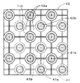
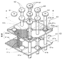
次に、本発明の実施の形態を図面に基づいて説明する。図1は本発明の一実施形態であるパッケージ基板10の平面図(円内は部分拡大図)、図2は図1のA−A断面図(要部)、図3は薄膜コンデンサ40を模式的に示した斜視図、図4は図3のB−B断面図である。
Next, embodiments of the present invention will be described with reference to the drawings. FIG. 1 is a plan view of a
本実施形態のパッケージ基板10は、図1に示すように、複数の電源用パッド61と、これらの電源用パッド61と同一層に設けられた複数のグランド用パッド62と、電源用パッド61及びグランド用パッド62の周囲に設けられた複数の信号用パッド63と、電源用パッド61同士を電気的に接続する電源用配線66と、複数のグランド用パッド62同士を電気的に接続するグランド用配線67と、各パッド61〜63の周囲に設けられたチップコンデンサ配置領域70とを備えている。本実施形態では、最表層であるソルダーレジスト層52から各パッド61,62,63やチップコンデンサ配置領域70の電源用パッド71,グランド用パッド72が外部に露出しており、電源用配線66とグランド用配線67は電源用パッド61やグランド用パッド62と同一層に形成されている。また、パッケージ基板10は、図2に示すように、コア基板20と、このコア基板20の表面に積層されたビルドアップ層30と、このビルドアップ層30に層間絶縁層46を介して積層された薄膜コンデンサ40と、この薄膜コンデンサ40に積層された電気絶縁性を有する応力緩和層50と、この応力緩和層50に積層されたソルダーレジスト層52とを備えている。また、ソルダーレジスト層52から露出している各パッド61,62には、それぞれはんだバンプ61d,62dが形成されている。
As shown in FIG. 1, the
コア基板20は、図2に示すように、BT(ビスマレイミド−トリアジン)樹脂やガラスエポキシ基板等からなるコア基板本体21と、このコア基板本体21の表裏両面に所定の配線パターンを持つように形成された銅製の導体層22(図2では表面側のみ示す)と、コア基板本体21の表裏を貫通するスルーホールの内周面に形成された銅からなるスルーホール導体24とを有しており、表裏両面の導体層22同士はスルーホール導体24を介して電気的に接続されている。
As shown in FIG. 2, the
ビルドアップ層30は、コア基板20の表面に樹脂絶縁層36と導体層32とを積層したものである。ここで、導体層32は、所定の配線パターンとなるように形成され、樹脂絶縁層36の表裏を貫通するバイアホール34を介して下層の導体層22と電気的に接続されている。このようなビルドアップ層30は、周知のサブトラクティブ法やアディティブ法(セミアディティブ法やフルアディティブ法を含む)により形成されるが、例えば以下のようにして形成される。すなわち、まず、コア基板20の表面に樹脂絶縁層36となる樹脂シートを貼り付ける。ここで、樹脂絶縁層36の常温でのヤング率は2〜7GPaである。この樹脂シートは、変成エポキシ系樹脂シート、ポリフェニレンエーテル系樹脂シート、ポリイミド系樹脂シート、シアノエステル系樹脂シートなどで形成され、その厚みは概ね20〜80μmであり、樹脂中にシリカ、アルミナ、ジルコニア等の無機成分が分散されていてもよい。本実施形態では、味の素社製の熱硬化性樹脂フィルム(品名:ABF−45SH、ヤング率:3.0GPa)を用いた。次に、貼り付けた樹脂シートに炭酸ガスレーザやUVレーザ、YAGレーザ、エキシマレーザなどによりブラインドホールを形成することにより樹脂シートを樹脂絶縁層36とし、続いてこの樹脂絶縁層36の表面(ブラインドホール内部を含む)を覆うようにベタパターンの導体層を形成する。このベタパターンの導体層は、無電解銅めっきの後に電解銅めっきを施すことにより形成される。なお、ブライドスルーホール内部の導体層がバイアホール34となる。そして、ベタパターンの導体層に所定の配線パターンを形成するために、導体層上にその配線パターンと同じパターンを持つレジストを印刷する。その後、エッチング液で処理してベタパターンの導体層のうちレジスト部分のみを残すことにより、所定の配線パターンを持つ導体層32を形成し、その後レジストを剥がす(テンティング法)。なお、図2には1層のビルドアップ層30を例示したが、この手順を繰り返すことにより多層のビルドアップ層としてもよい。また、図2にはビルドアップ層30をコア基板20の表面に形成した場合を例示したが、コア基板20の裏面にもビルドアップ層30を形成してもよい。
The
薄膜コンデンサ40は、図2に示すように、セラミック系の高誘電体材料を高温で焼成した高誘電体層43と、この高誘電体層43を挟む銅製の第1薄膜電極41及び第2薄膜電極42とで構成されている。本実施形態では第1薄膜電極41は電源電極つまり+極であり、第2薄膜電極42はグランド電極つまり−極である。
As shown in FIG. 2, the
第1薄膜電極41は、図2〜図4に示すようにいわゆるベタパターンを複数の第1薄膜小電極41aに分割したものであり、各第1薄膜小電極41aは、この第1薄膜小電極41aを上下方向に貫通する電源用ポスト61aと貫通部位にて電気的に接続されている。この電源用ポスト61aは、ビルドアップ層30の導体層32のうちの電源用ラインに接続され、第2薄膜電極42と同じ層にこの第2薄膜電極42とは独立した円形のランド61cを有している。このランド61cは、第2薄膜電極42に設けられたクリアランスホール42bにより第2薄膜小電極42aとは電気的に絶縁されており、応力緩和層50を貫通するバイアホール61bを介して電源用パッド61に電気的に接続されている。したがって、各第1薄膜小電極41aは、電源用ポスト61a、ランド61c及びバイアホール61bを介して電源用パッド61に電気的に接続され、電源用ポスト61aを介して下層の電源用ラインに電気的に接続されているが、グランド用ラインとは絶縁されている。本実施形態では、薄膜コンデンサ40よりも上層に形成された電源用配線66(図1参照)によって各電源用パッド61が電気的に接続されているため、各第1薄膜小電極41aは同電位(電源電位)になる。
The first
また、第2薄膜電極42も、ベタパターンを複数の第2薄膜小電極42aに分割したものであり、各第2薄膜小電極42aは、下方に伸びるグランド用ポスト62aや上方に伸びるバイアホール62bと電気的に接続されている。グランド用ポスト62aは、第1薄膜電極41に設けられたクリアランスホール41bにより第1薄膜小電極41aとは電気的に絶縁され、下端側にてビルドアップ層30の導体層32のうちのグランド用ラインに電気的に接続されている。また、バイアホール62bは、応力緩和層50を貫通しグランド用パッド62と第2薄膜小電極42aとを電気的に接続している。したがって、各第2薄膜小電極42aは、グランド用ポスト62aを介して下層のグランド用ラインに電気的に接続され、バイアホール62bを介してグランド用パッド62に電気的に接続されているが、電源用ラインとは絶縁されている。本実施形態では、薄膜コンデンサ40よりも上層に形成されたグランド用配線67(図1参照)によって各グランド用パッド62が電気的に接続されているため、各第2薄膜小電極42aは同電位(グランド電位)になる。
The second
また、高誘電体層43は、BaTiO3、SrTiO3、TaO3、Ta2O5、PZT、PLZT、PNZT、PCZT、PSZTからなる群より選ばれた1種又は2種以上の金属酸化物を含んでなる高誘電体材料を0.1〜10μmの薄膜状にしたあと焼成してセラミックにしたものである。この高誘電体層43の厚さ(つまり第1及び第2薄膜電極41,42の間の距離)は10μm以下であってピンホール等がなければ実質的に短絡しない距離に設定されている。
The
ここで、図5は短絡した第1及び第2薄膜小電極が存在するパッケージ基板の部分断面図であり、図6はこのパッケージ基板の薄膜コンデンサの模式的な斜視図である。図5及び図6に示すように、複数の第1薄膜小電極41aと複数の第2薄膜小電極42aのうち高誘電体層43のピンホールPを介して電気的に短絡している第1薄膜小電極41aaと第2薄膜小電極42aaが存在している場合、その第1薄膜小電極41aaには電源用ポスト61aやバイアホール61bが形成されておらず、その第2薄膜小電極42aaにはグランド用ポスト62aやバイアホール62bが形成されていない。この結果、短絡している両小電極41aa,42aaは、電源用ラインともグランド用ラインとも電気的に接続されていない状態となり、電源電位やグランド電位とは独立した電位となる。この結果、薄膜コンデンサ40のうち、短絡している両小電極41aa,42aaが高誘電体層43を挟み込んでいる部分のみコンデンサの機能を失い、他の薄膜小電極41a,42aが高誘電体層43を挟み込んでいる部分はコンデンサの機能を維持する。
Here, FIG. 5 is a partial cross-sectional view of the package substrate where the short-circuited first and second thin film small electrodes exist, and FIG. 6 is a schematic perspective view of the thin film capacitor of the package substrate. As shown in FIGS. 5 and 6, the first short-circuited between the plurality of first thin-film
図2に戻り、応力緩和層50は、薄膜コンデンサ40に積層されており、弾性材料で形成されている。弾性材料としては特に限定されないが、例えば、変成エポキシ系樹脂シート、ポリフェニレンエーテル系樹脂シート、ポリイミド系樹脂シート、シアノエステル系樹脂シート及びイミド系樹脂シートなどの有機系樹脂シートが挙げられる。これらの有機系樹脂シートは、熱可塑性樹脂であるポリオレフィン系樹脂やポリイミド系樹脂、熱硬化性樹脂であるシリコーン樹脂やSBR、NBR、ウレタン等のゴム系樹脂を含有していてもよいし、シリカ、アルミナ、ジルコニア等の無機系の繊維状、フィラー状、扁平状を含有していてもよい。この応力緩和層50は、ヤング率が10〜1000MPaと低い値であることが好ましい。応力緩和層50のヤング率がこの範囲だと、実装される半導体素子80とパッケージ基板10との間に熱膨張係数差に起因する応力が発生したとしても、その応力を緩和することができる。なお、この応力緩和層50を形成する材料として、前出の樹脂絶縁層36と同じ材料を用いてもよい。
Returning to FIG. 2, the
パッケージ基板10の表面は、半導体素子80を実装する面である。この実装面のうち半導体素子80の直下領域には、電源用パッド61及びグランド用パッド62が格子状又は千鳥状に配列され、この領域の周囲には信号用パッド63が配列されている(図1参照)。更に信号用パッド63の周囲には、チップコンデンサ配置領域70が複数形成されている。このチップコンデンサ配置領域70は、チップコンデンサの電源用端子及びグランド用端子とそれぞれ接続するための電源用パッド71及びグランド用パッド72が複数対形成されている。なお、各電源用パッド71は薄膜コンデンサ40の第1薄膜電極41を介して外部電源の負極に接続され、各グランド用パッド72は第2薄膜電極42を介して外部電源の正極に接続される。
The surface of the
ソルダーレジスト層52は、各パッド61,62,63,71,72に対応する位置で開口している。このソルダーレジスト層52は、例えば電源用パッド61上のはんだバンプ61dやグランド用パッド62上のはんだバンプ62dについていえば、半導体素子80を実装する際に溶融したはんだが周囲に流出しないようにするソルダーダムの機能を果たす。
The solder resist
次に、このように構成されたパッケージ基板10の使用例について説明する。まず、チップコンデンサの電源用端子とグランド用端子をそれぞれチップコンデンサ配置領域70の電源用パッド71とグランド用パッド72にはんだにより接合する。次に、半導体素子80をパッケージ基板10に載置する。このとき、半導体素子80の裏面に設けられた多数の電源用端子81、グランド用端子82がそれぞれ対応する電源用パッド61のはんだバンプ61dやグランド用パッド62のはんだバンプ62dと合致するように載置する。続いて、リフローにより各端子と各パッドとをはんだで接合する。その後、パッケージ基板10のうち実装面とは反対側の面をマザーボード等の他のプリント配線板に接合する。このとき、予めパッケージ基板10の裏面に形成されたパッドにはんだバンプを形成しておき、他のプリント配線板上の対応するパッドと接触させた状態でリフローにより接合する。
Next, a usage example of the
次に、本実施形態のパッケージ基板10の製造例について説明する。コア基板20及びビルドアップ層30の作製手順は周知であるため、ここでは薄膜コンデンサ40及び応力緩和層50を作製する手順を中心に説明する。図7〜図12はこの手順の説明図である。
Next, a manufacturing example of the
まず、図7(a)に示す薄膜コンデンサ40を作製した。この薄膜コンデンサ40の作製手順について説明する。
(1)乾燥窒素中において、濃度1.0モル/リットルとなるように秤量したジエトキシバリウムとビテトライソプロポキシドチタンとを、脱水したメタノールと2−メトキシエタノールとの混合溶媒(体積比3:2)に溶解し、室温の窒素雰囲気下で3日間攪拌してバリウムとチタンのアルコキシド前駆体組成物溶液を調整した。次いで、この前駆体組成物溶液を0℃に保ちながら攪拌し、あらかじめ脱炭酸した水を0.5マイクロリットル/分の速度で窒素気流中で噴霧して加水分解した。
(2)このようにして作製されたゾルーゲル溶液を、0.2ミクロンのフィルタを通し、析出物等をろ過した。
(3)上記(2)で作製したろ過液を厚さ12μmの銅箔(第1薄膜電極41となる)上に1500rpmで1分間スピンコートした。このスピンコートした基板を150℃に保持されたホットプレート上に3分間置き乾燥した。その後基板を850℃に保持された電気炉中に挿入し、15分間焼成を行った。ここで、1回のスピンコート/乾燥/焼成で得られる膜厚が0.03μmとなるようゾルーゲル液の粘度を調整した。なお、第1薄膜電極41としては銅の他に、ニッケル、白金、金、銀等を用いることもできる。
(4)スピンコート/乾燥/焼成を40回繰り返し1.2μmの高誘電体層43を得た。
(5)その後、スパッタ等の真空蒸着装置を用いて高誘電体層43の上に銅層を形成し更にこの銅層上に電解めっき等で銅を10μm程度足すことにより、銅箔142(後に第2薄膜電極42の一部をなす)を形成した。このようにして、薄膜コンデンサ40を得た。誘電特性は、INPEDANCE/GAIN PHASE ANALYZER(ヒューレットパッカード社製、品名:4194A)を用い、周波数1kHz、温度25℃、OSCレベル1Vという条件で測定したところ、その比誘電率は、1,850であった。なお、真空蒸着は銅以外に白金、金等の金属層を形成してもよいし、電解めっきも銅以外にニッケル、スズ等の金属層を形成してもよい。また、高誘電体層43をチタン酸バリウムとしたが、他のゾル−ゲル溶液を用いることで、高誘電体層43をチタン酸ストロンチウム(SrTiO3)、酸化タンタル(TaO3、Ta2O5)、チタン酸ジルコン酸鉛(PZT)、チタン酸ジルコン酸ランタン鉛(PLZT)、チタン酸ジルコン酸ニオブ鉛(PNZT)、チタン酸ジルコン酸カルシウム鉛(PCZT)及びチタン酸ジルコン酸ストロンチウム鉛(PSZT)のいずれかにすることも可能である。
First, the
(1) In dry nitrogen, diethoxybarium and bitetraisopropoxide titanium weighed so as to have a concentration of 1.0 mol / liter are mixed solvents of dehydrated methanol and 2-methoxyethanol (volume ratio 3: It was dissolved in 2) and stirred for 3 days in a nitrogen atmosphere at room temperature to prepare an alkoxide precursor composition solution of barium and titanium. Next, this precursor composition solution was stirred while being kept at 0 ° C., and hydrolyzed by spraying predecarboxylated water in a nitrogen stream at a rate of 0.5 microliter / minute.
(2) The sol-gel solution thus prepared was passed through a 0.2 micron filter, and precipitates and the like were filtered.
(3) The filtrate prepared in the above (2) was spin-coated on a copper foil having a thickness of 12 μm (to be the first thin film electrode 41) at 1500 rpm for 1 minute. The spin-coated substrate was placed on a hot plate maintained at 150 ° C. for 3 minutes and dried. Thereafter, the substrate was inserted into an electric furnace maintained at 850 ° C. and baked for 15 minutes. Here, the viscosity of the sol-gel solution was adjusted so that the film thickness obtained by one spin coating / drying / firing became 0.03 μm. As the first
(4) Spin coating / drying / firing was repeated 40 times to obtain a 1.2 μm
(5) Thereafter, a copper layer is formed on the
なお、薄膜コンデンサ40のその他の作製方法として、以下の方法もある。即ち、チタン酸バリウム粉末(富士チタン工業株式会社製、HPBTシリーズ)を、チタン酸バリウム粉末の全重量に対して、ポリビニルアルコール5重量部、純水50重量部および溶剤系可塑剤としてフタル酸ジオクチルまたはフタル酸ジブチル1重量部の割合で混合されたバインダ溶液に分散させ、これをロールコータ、ドクターブレード、αコータ等の印刷機を用いて、厚さ12μmの銅箔(後に第1薄膜電極41となる)に、厚さ5〜7μm程度の薄膜状に印刷し、60℃で1時間、80℃で3時間、100℃で1時間、120℃で1時間、150℃で3時間乾燥し未焼成層とする。BaTiO3以外にSrTiO3、TaO3、Ta2O5、PZT、PLZT、PNZT、PCZT、PSZTからなる群より選ばれた1種又は2種以上の金属酸化物を含んでなるペーストをロールコータ、ドクターブレード等の印刷機を用いて、厚さ0.1〜10μmの薄膜状に印刷、乾燥し未焼成層としてもよい。印刷後、この未焼成層を600〜950℃の温度範囲で焼成し、高誘電体層43とする。その後、スパッタ等の真空蒸着装置を用いて高誘電体層43の上に銅層を形成し更にこの銅層上に電解めっき等で銅を10μm程度足すことにより、銅箔142(後に第2薄膜電極42の一部をなす)を形成する。なお、真空蒸着は銅以外に白金、金等の金属層を形成してもよいし、電解めっきも銅以外にニッケル、スズ等の金属層を形成してもよい。その他、チタン酸バリウムをターゲットにしたスッパタ法でも可能である。
As another method for manufacturing the
続いて、図7(b)に示すように、薄膜コンデンサ40の第1薄膜電極41を線状溝41cにより複数の第1薄膜小電極41aに分割すると共にクリアランスホール41bを形成した。具体的には、第1薄膜電極41にレジストを積層し、そのレジストにフォトマスクを介して露光・現像することにより、形成しようとするクリアランスホール41bと格子状の線状溝41cとを除く領域を覆うようにレジストパターンを形成し、続いてエッチング液で処理して第1薄膜電極41のうちレジストで覆われていない部分を除去することにより第1薄膜電極41にクリアランスホール41bと格子状の線状溝41cとを形成し、その後レジストを剥離した。この結果、第1薄膜電極41が線状溝41cにより複数の第1薄膜小電極41aに分割された。ここで、線状溝41cの溝幅は、この線状溝41cに絶縁性樹脂が充填されたときに隣り合う第1薄膜小電極41a同士の絶縁が維持される幅に設定した。なお、エッチング工程では、塩化第二銅エッチング液を使用したが、高誘電体層43を僅かに浸食する深さまでエッチングされた状態となるように短時間で処理した。
Subsequently, as shown in FIG. 7B, the first
続いて、図7(c)に示すように、この薄膜コンデンサ40の銅箔142を複数の線状溝142cにより複数の銅小片142aに分割すると共にクリアランスホール142bを形成した。ここで、銅小片142aは、その中心がクリアランスホール41bの中心線上に位置するように形成し、クリアランスホール142bは、その中心が第1薄膜小電極41aの中心線上に位置するように形成した。具体的には、銅箔142上にレジストを積層し、そのレジストにフォトマスクを介して露光・現像することにより、形成しようとするクリアランスホール142bと格子状の線状溝142cとを除く領域を覆うようにレジストパターンを形成し、続いてエッチング液で処理して銅箔142のうちレジストで覆われていない部分を除去することにより銅箔142にクリアランスホール142bと格子状の線状溝142cとを形成し、その後レジストを剥離した。この結果、銅箔142が線状溝142cにより複数の銅小片142aに分割された。ここで、線状溝142cの溝幅は、この線状溝142cに絶縁性樹脂が充填されたときに隣り合う銅小片142a同士の絶縁が維持される幅に設定した。なお、エッチング工程では、塩化第二銅エッチング液を使用したが、高誘電体層43を僅かに浸食する深さまでエッチングされた状態となるように短時間で処理した。
Subsequently, as shown in FIG. 7C, the
このあと、高誘電体層43にピンホールが発生している箇所があるか否かを探す検査を行った。この段階では、第1薄膜電極41及び銅箔142は模式的には図8に示す状態になっている。即ち、第1薄膜電極41は線状溝41cによって複数の第1薄膜小電極41aに分割され、銅箔142も線状溝142cによって複数の銅小片142aに分割されている。ここで、第1薄膜小電極41aのうち図8にて網掛けした第1薄膜小電極Sを例に挙げて説明する。銅箔142を平面視したときに、高誘電体層43を介して第1薄膜小電極Sと重なり合うのは、上部金属層である銅箔142の銅小片142aのうち図8にて網掛けした銅小片T,U,V,Wの4つである。このため、第1薄膜小電極Sと各銅小片T,U,V,Wとの間に電流が流れるか否かを調べることにより、これらの間の高誘電体層43にピンホールが生じているか否かがわかる。そして、第1薄膜小電極Sと各金属小片T,U,V,Wとの間に電流が流れなかったときには、これらの間の高誘電体層43にピンホール等の不要な導体部分が生じていないと判断され、第1薄膜小電極Sと例えば銅小片Uとの間にだけ電流が流れたときには、両者の間の高誘電体層43にピンホール等の不要な導体部分が生じていると判断される。そして、互いに対向するすべての第1薄膜小電極41aと第2薄膜小電極141について検査を行い、どこにも不要な導体部分が生じていないと判断されたときには、後述する工程を経て最終的に図2の断面構造となるようにパッケージ基板10を作製した。一方、いずれかに不要な導体部分が生じていると判断されたときには、最終的に図5の断面構造となるようにパッケージ基板10を作製した。
Thereafter, an inspection was performed to find out whether or not there is a portion where pinholes are generated in the
さて、検査の結果、高誘電体層43にピンホールが発生している箇所がなかった場合には、図9及び図10に示す手順にしたがってパッケージ基板10を形成した。まず、図9(a)に示すように、コア基板20(図9では省略、図2参照)の少なくとも片面にビルドアップ層30を形成した基板を用意し、この基板のビルドアップ層30の上にピンラミネート法により層間絶縁層46と図7(c)に示す薄膜コンデンサ40との位置合わせを行い、温度50〜150℃、圧力0.5〜1.5MPaという条件下で貼り付けた。その後150℃で30分乾燥した(図9(b)参照)。これにより、第1薄膜電極41のクリアランスホール41b及び線状溝41c(図7(b)参照)には、層間絶縁層46が充填された。続いて、作製途中の基板のうちクリアランスホール41bの中心の直上位置とクリアランスホール142bの中心位置に、炭酸ガスレーザやUVレーザ、YAGレーザ、エキシマレーザなどによりビルドアップ層30の導体層32の表面に達するブラインドホール161a,162aを形成した(図9(c)参照)。このとき、ブラインドホール162aの径がクリアランスホール41bの径よりも小さくなるようにレーザの出力を調整した。ここでは、高誘電体層43にピンホール等の不要な導体部分が生じていないため、すべてのクリアランスホール41b,142bにつきブラインドホール161a,162aを形成した。続いて、黒色酸化処理を施すことにより表面を粗化し、粗化面に触媒を付与したあと無電解銅めっきを行い、更に電解銅めっきを行うことにより、ブラインドホール161a,162aの内部を銅で充填すると共に表面全体を銅で覆った(図9(d)参照)。なお、ブラインドホール161a,162aの内部に充填された銅がそれぞれ図2の電源用ポスト61a及びグランド用ポスト62aとなる。また、高誘電体層43の上面は、線状溝142cが銅で埋められて銅小片142aが一体化されることによりベタパターンの銅層144となる。
As a result of the inspection, when there was no location where pinholes were generated in the
続いて、銅層144にハーフエッチングを施すことにより銅層144の厚さを12μmとしたあと、この薄くなった銅層144に所定の配線パターンを形成するために、その配線パターンと同じパターンを持つレジスト148を印刷した(図9(e)参照)。このときレジスト148は、先ほど銅箔142を分割して銅小片142aを形成した際の線状溝142cの領域及びクリアランスホール142bからそれより小径のランド61c(図2参照)を差し引いたドーナツ形状の領域の両方を除く領域に印刷した。その後、エッチング液で処理してベタパターンの銅層144のうちレジスト148の下方部分のみを残すことにより、高誘電体層43の上面に第2薄膜小電極42aとクリアランスホール42bとランド61cを形成すると共に(図10(a)参照)、第2薄膜小電極42a同士の間に線状溝42c(図6参照)を形成した(テンティング法)。なお、これ以降、銅層144を第2薄膜電極42と称する。
Subsequently, after half-etching the
次に、この作製途中の基板の上に応力緩和層50を真空ラミネータで温度50〜150℃、圧力0.5〜1.5MPaというラミネート条件下で貼り付け、150℃で3時間硬化した(図10(b)参照)。この応力緩和層50は、変成エポキシ系樹脂シート、ポリフェニレンエーテル系樹脂シート、ポリイミド系樹脂シート、シアノエステル系樹脂シート又はイミド系樹脂シートであり、熱可塑性樹脂であるポリオレフィン系樹脂やポリイミド系樹脂、熱硬化性樹脂であるシリコーン樹脂やSBR、NBR、ウレタン等のゴム系樹脂を含有していてもよいし、シリカ、アルミナ、ジルコニア等の無機系の繊維状、フィラー状、扁平状のものが分散していてもよい。また、この応力緩和層50のヤング率は10〜1000MPaが好ましい。このような応力緩和層50の作製例を以下に示す。すなわち、ナフタレン型のエポキシ樹脂(日本化薬(株)製、商品名:NC−7000L)100重量部、フェノール−キシリレングリコール縮合樹脂(三井化学製、商品名:XLC−LL)20重量部、架橋ゴム粒子としてTgが−50℃のカルボン酸変性NBR(JSR(株)製、商品名:XER−91)90重量部、1−シアノエチル−2−エチル−4−メチルイミダゾール4重量部を乳酸エチル300重量部に溶解した樹脂組成物をロールコータ(サーマトロニクス貿易製)を使用して、ポリメチルペンテン(TPX)(三井石油化学工業製、商品名:オピュランX−88)製の42〜45μm厚のフィルム上に塗布し、その後、80℃で2時間、120℃で1時間、150℃で30分乾燥させて厚さ40μmの応力緩和シートとした。なお、このようにして作製した応力緩和層50は、30℃でヤング率が500MPaであった。
Next, the
次いで、応力緩和層50の所定位置にCO2レーザにて、φ1.4mmのマスク径を介して2.0mjのエネルギー密度、1ショットでブラインドホール161b,162bを形成した(図10(c)参照)。続いて、粗化処理し、150℃で3時間乾燥硬化し応力緩和層50を完全硬化した。その後、触媒付与、化学銅、めっきレジスト形成、電気銅めっき、めっきレジスト剥離、クイックエチングの工程を施すことにより、ブラインドホール161b,162bを銅で充填してバイアホール61b,62bを形成すると共に各バイアホール61b,62bの上面に電源用パッド61及びグランド用パッド62を形成した(図10(d)参照)。なお、図示しないが、図1に示す信号用パッド63や電源用配線66、グランド用配線67、パッド71,72等も同時に形成した。続いて、ソルダーレジスト層52として感光性ドライフィルムを真空ラミネータにより積層し、露光・現像することによりソルダーレジスト層52の各パッド61,62に対向する位置に開口を形成し、その後紫外線照射及び加熱処理を施すことによりソルダーレジスト層52を完全に硬化させた。続いて、図示しないメタルマスクを用いてはんだペーストを印刷することにより開口内にはんだペーストを充填し、その後メタルマスクを外し、リフローすることによりはんだバンプ61d,62dを作製した(図10(e)参照)。これにより、図2に示したパッケージ基板10が完成した。なお、図示しないが、ソルダーレジスト層52のうち信号用パッド63に対向する位置には開口を形成すると共にはんだバンプを作製し、パッド71,72に対向する位置には開口のみ設けた。
Then, at a CO 2 laser at a predetermined position of the
ところで、高誘電体層43にピンホールが発生している箇所の検査において、図8の例えば第1薄膜小電極Sと銅小片Tとの間にだけ電流が流れたときには、両者の間の高誘電体層43にピンホール等の不要な導体部分(ここではピンホールPという)が生じているため、最終的に図5の断面構造となるようにパッケージ基板10を作製する。図5のパッケージ基板10の作製手順は基本的には図2のパッケージ基板10の作製手順と同じであるため、両作製手順で異なる部分のみを図11及び図12に基づいて以下に説明する。なお、図11(a)〜(e)の工程は図9(a)〜(e)の工程に対応し、図12(a)〜(e)の工程は図10(a)〜(e)の工程に対応する。
By the way, in the inspection of the location where the pinhole is generated in the
まず、ビルドアップ層30の上にピンラミネート法により層間絶縁層46と薄膜コンデンサ40との位置合わせを行い(図11(a)参照)、これらを貼り付けた(図11(b)参照)。続いて、クリアランスホール41bの中心の直上位置とクリアランスホール142bの中心位置にブラインドホール161a,162aを形成した(図11(c)参照)。このとき、ピンホールPにより導通している第1薄膜小電極Sと銅小片Uにはブラインドホール161a,162aを形成しなかった。続いて、銅めっきによりブラインドホール161a,162aの内部を銅で充填して電源用ポスト61a及びグランド用ポスト62aとすると共に表面全体を銅で覆ってベタパターンの銅層144とした(図11(d)参照)。次に、銅層144の厚さを薄くしたあとレジスト148を印刷し(図11(e)参照)、エッチング液で処理することにより高誘電体層43の上面に第2薄膜小電極42aとクリアランスホール42bとランド61cを形成すると共に(図12(a)参照)、第2薄膜小電極42a同士の間に線状溝42c(図2参照)を形成した(テンティング法)。なお、これ以降、銅層144を第2薄膜電極42と称する。また、第1薄膜小電極Sを第1薄膜小電極41aaと称し、銅小片Sの位置にある第2薄膜小電極42aを第2薄膜小電極42aaと称する。次に、応力緩和層50を真空ラミネータで貼り付けたあと(図12(b)参照)、応力緩和層50の所定位置にブラインドホール161b,162bを形成した(図12(c)参照)。このとき、第1薄膜小電極41aa及び第2薄膜小電極42aaの直上位置にはブラインドホール161b,162bを形成しなかった。その後、ブラインドホール161b,162bを銅で充填してバイアホール61b,62bを形成すると共に各バイアホール61b,62bの上面に電源用パッド61及びグランド用パッド62を形成した(図12(d)参照)。このとき、第1薄膜小電極41aa及び第2薄膜小電極42aaの直上位置にもそれぞれ電源用パッド61及びグランド用パッド62を形成した。なお、図示しないが、図1に示す信号用パッド63や電源用配線66、グランド用配線67、パッド71,72等も同時に形成した。続いて、ソルダーレジスト層52を積層し、ソルダーレジスト層52の各パッド61,62に対向する位置に開口を形成し、その後はんだペーストを印刷することにより開口内にはんだペーストを充填し、リフローすることによりはんだバンプ61d,62dを作製した(図12(e)参照)。このようにして、図5に示したパッケージ基板10を作製した。
First, the
以上詳述したパッケージ基板10では、薄膜コンデンサ40を構成する複数の第1薄膜小電極41aと複数の第2薄膜小電極42aのうち高誘電体層43に生じた不要な導体部分(例えばピンホールP)を介して電気的に短絡している第1薄膜小電極41aaと第2薄膜小電極42aaは、電源電位ともグランド電位とも独立するように配線されているため、互いに対向し電気的に絶縁されている他の第1薄膜小電極41aと第2薄膜小電極42aとの間を短絡させてしまうことはない。この結果、互いに対向し電気的に絶縁されている他の第1薄膜小電極41aと第2薄膜小電極42aは、依然としてコンデンサの機能を発揮する。したがって、薄膜コンデンサ40の電極間に短絡が生じたとしても該薄膜コンデンサ40はコンデンサの性能を維持することができ、コンデンサ内蔵パッケージ基板10の歩留まりの悪化を防止することができる。
In the
また、薄膜コンデンサ40は、誘電率が高く厚さ10μm以下のセラミックにより作製された高誘電体層43を有しているうえ、第1及び第2薄膜電極41,42がいわゆるベタパターンを線状溝41c,42cにより切断したものであり面積が十分大きいため、静電容量を十分大きくすることができる。その結果、半導体素子80のオンオフの周波数が数GHz〜数10GHzと高く電位の瞬時低下が起きやすい状況下であっても十分なデカップリング効果を発揮する。また、この高誘電体層43は、作製途中の基板上で焼成するのではなく、別に高誘電体材料を焼成して作製したものを作製途中の基板に組み込むため、容易に組み込むことができる。
The
更に、電源用ポスト61aとグランド用ポスト62aは、半導体素子80の直下領域で格子状又は千鳥状に交互に並んでいるため、ループインダクタンスが低くなり、半導体素子80の電源電位の瞬時低下を防止しやすくなる。 Furthermore, since the power supply posts 61a and the ground posts 62a are alternately arranged in a lattice or zigzag pattern in the region immediately below the semiconductor element 80, the loop inductance is reduced, and an instantaneous decrease in the power supply potential of the semiconductor element 80 is prevented. It becomes easy to do.
更にまた、半導体素子80とパッケージ基板10との間に熱膨張係数差に起因する応力が発生したとしても、応力緩和層50がその応力を吸収するため不具合が発生しにくい。
Furthermore, even if a stress due to the difference in thermal expansion coefficient is generated between the semiconductor element 80 and the
なお、本発明は上述した実施形態に何ら限定されることはなく、本発明の技術的範囲に属する限り種々の態様で実施し得ることはいうまでもない。 It should be noted that the present invention is not limited to the above-described embodiment, and it goes without saying that the present invention can be implemented in various modes as long as it belongs to the technical scope of the present invention.
例えば、上述した実施形態では、図5に示すように、高誘電体層43のピンホールPを介して電気的に短絡している第1薄膜小電極41aaと第2薄膜小電極42aaが存在している場合には、第1薄膜小電極41aaに電源用ポスト61aやバイアホール61bを形成せず、第2薄膜小電極42aaにもグランド用ポスト62aやバイアホール62bを形成しないようにしたが、図13に示す構造を採用してもよい。この図13に示す構造では、第1薄膜小電極41aaには電源用ポスト61aやバイアホール61bが形成されていないが、第2薄膜小電極42aaにはグランド用ポスト62aやバイアホール62bが形成されている。この構造では、第2薄膜小電極42aaはグランド電位となるため、これと短絡している第1薄膜小電極41aaもグランド電位となるが、第1薄膜小電極41aaはその直上の電源用パッド61にもその下層のビルドアップ層30にも電気的に接続されていないため、電源電位とは独立した電位となる。このため、薄膜コンデンサ40はピンホールPが存在するにもかかわらずコンデンサの性能を維持することができ、これによりパッケージ基板10の歩留まりの悪化を防止することができる。
For example, in the above-described embodiment, as shown in FIG. 5, there are the first thin film small electrode 41aa and the second thin film small electrode 42aa that are electrically short-circuited through the pinhole P of the
あるいは、図14の構造を採用してもよい。この図14に示す構造では、第1薄膜小電極41aaには電源用ポスト61aやバイアホール61bが形成されているが、第2薄膜小電極42aaにはグランド用ポスト62aやバイアホール62bが形成されていない。この構造では、第1薄膜小電極41aaは電源電位となるため、これと短絡している第2薄膜小電極42aaも電源電位となるが、第2薄膜小電極42aaはその直上のグランド用パッド62にもその下層のビルドアップ層30にも電気的に接続されていないため、グランド電位とは独立した電位となる。このため、薄膜コンデンサ40はピンホールPが存在するにもかかわらずコンデンサの性能を維持することができ、これによりパッケージ基板10の歩留まりの悪化を防止することができる。
Or you may employ | adopt the structure of FIG. In the structure shown in FIG. 14, a
なお、図12(d)や図13では第1薄膜小電極41aaの直上のバイアホール61bを形成しないようにしたが、このバイアホール61bを形成したとしても薄膜コンデンサ40の機能を損なわないため、形成しても構わない。
In FIG. 12 (d) and FIG. 13, the via
また、上述した実施形態では、片面に第1薄膜小電極41aを形成すると共にもう一方の面に銅小片142aを形成した薄膜コンデンサ40を基板に積層する前の段階で検査することにより高誘電体層43にピンホールPが発生しているか否かの検査を行ったが、検査するタイミングはこれに限るものではない。例えば、第1薄膜電極41のみに線状溝41cとクリアランスホール41bとを形成して多数の第1薄膜小電極41aとした薄膜コンデンサ40をビルドアップ層30の上に層間絶縁層46を介して貼り付け(図15(a)参照)、続いてテンティング法にて銅箔142をエッチングすることにより多数の銅小片142aとクリアランスホール142bとを形成すると共にクリアランスホール142b内の高誘電体層43を除去して第1薄膜小電極41aを露出させ(図15(b)参照)、この段階で第1薄膜小電極41aのうちクリアランスホール142bから露出している部分と銅小片142aのうちその第1薄膜小電極41aにオーバーラップしているものとの間で電流が流れるか否かを検査してもよい。ここで、銅箔142のエッチングは、エッチング液として塩化第二銅エッチング液を使用し、銅箔142及び高誘電体層43をエッチングしたあと第1薄膜電極41が僅かにエッチングされた状態となるように短時間で処理する。その後、第1薄膜小電極41aのうち外部に露出している部分に絶縁樹脂を埋め込み表面を平坦化し(図15(c)参照)、クリアランスホール41bの中心の直上位置とクリアランスホール142bの中心位置にブラインドホール161a,162aを形成する(図15(d)参照)。このとき、ピンホールPにより第1薄膜小電極Sと銅小片Uとが導通していたとすると、第1薄膜小電極Sと銅小片Uにはブラインドホール161a,162aを形成しない。その後の手順は図11(d)〜図11(e)及び図12(a)〜図12(e)と同様であるためその説明を省略するが、結果として図15(e)に示すパッケージ基板10が得られる。
In the above-described embodiment, the high-dielectric material is obtained by inspecting the
また、上述した実施形態では、第1薄膜電極41と高誘電体層43と第2薄膜電極42とを一層ずつ設けた薄膜コンデンサ40について例示したが、図16のコンデンサ部550と同様、第1薄膜電極41と高誘電体層43と第2薄膜電極42とを交互に複数層設けるようにしてもよい。
In the above-described embodiment, the
更に、上述した実施形態では、チップコンデンサ配置領域70にチップコンデンサを搭載する構成を採用したが、薄膜コンデンサ40だけで静電容量が十分足りる場合には、チップコンデンサ配置領域70を廃止してもよい。こうすれば、パッケージ基板10をコンパクト化することができる。
Further, in the above-described embodiment, the configuration in which the chip capacitor is mounted in the chip
更にまた、上述した実施形態では、セラミック製の高誘電体層43を採用したが、セラミック系の高誘電体材料を無機フィラーとして配合した有機樹脂からなる高誘電体層43としてもよい。
Furthermore, in the above-described embodiment, the ceramic
そして更に、応力緩和層50は、パッケージ基板10の全面にわたって設けられていてもよいが、実装される半導体素子80の直下にのみ形成されていてもよい。熱膨張係数差による応力が問題となるのは主として半導体素子80の直下であるため、この部分に応力緩和層50を形成すれば材料コストを抑えることができる。
Furthermore, although the
そして更にまた、上述した実施形態では、電源用配線66とグランド用配線67を、電源用パッド61やグランド用パッド62と同じ層に形成したが、パッド61,62とは別の層に形成していてもよい。例えば、パッド61,62と薄膜コンデンサ40との間に形成されていてもよいし、薄膜コンデンサ40より下層(ビルドアップ層30やコア基板20)に形成されていてもよい。
In the above-described embodiment, the
10 パッケージ基板、20 コア基板、21 コア基板本体、22 導体層、24 スルーホール導体、30 ビルドアップ層、32 導体層、34 バイアホール、36 樹脂絶縁層、40 薄膜コンデンサ、41 第1薄膜電極、41a 第1薄膜小電極、41aa 第1薄膜小電極、41b クリアランスホール、41c 線状溝、42 第2薄膜電極、42a 第2薄膜小電極、42aa 第2薄膜小電極、42b クリアランスホール、42c 線状溝、43 高誘電体層、46 層間絶縁層、50 応力緩和層、52 ソルダーレジスト層、61 電源用パッド、61a 電源用ポスト、61b バイアホール、61c ランド、61d,62d バンプ、62 グランド用パッド、62a グランド用ポスト、62b バイアホール、63 信号用パッド、66 電源用配線、67 グランド用配線、70 チップコンデンサ配置領域、71 電源用パッド、72 グランド用パッド、80 半導体素子、81 電源用端子、82 グランド用端子、142 銅箔、142a 銅小片、142b クリアランスホール、142c 線状溝、144 銅層、148 レジスト、161a,162a ブラインドホール、161b,162b ブラインドホール。
10 package substrate, 20 core substrate, 21 core substrate body, 22 conductor layer, 24 through-hole conductor, 30 build-up layer, 32 conductor layer, 34 via hole, 36 resin insulation layer, 40 thin film capacitor, 41 first thin film electrode, 41a first thin film small electrode, 41aa first thin film small electrode, 41b clearance hole, 41c linear groove, 42 second thin film electrode, 42a second thin film small electrode, 42aa second thin film small electrode, 42b clearance hole, 42c linear Groove, 43 high dielectric layer, 46 interlayer insulating layer, 50 stress relaxation layer, 52 solder resist layer, 61 power supply pad, 61a power supply post, 61b via hole, 61c land, 61d, 62d bump, 62 ground pad, 62a Post for ground, 62b Via hole, 63 For
Claims (12)
前記電源用パッドと同一層に設けられた複数のグランド用パッドと、
前記電源用パッド及び前記グランド用パッドが設けられた層と少なくとも絶縁層を介して設けられ高誘電体層と該高誘電体を挟む第1及び第2薄膜電極とを有し前記第1薄膜電極は複数の第1薄膜小電極を含んでなり前記第2薄膜電極は複数の第2薄膜小電極を含んでなる薄膜コンデンサと、
前記複数の第1薄膜小電極と前記複数の第2薄膜小電極のうち電気的に絶縁されている第1薄膜小電極及び第2薄膜小電極については一方が電源電位となるように配線すると共に他方がグランド電位となるように配線し、前記複数の第1薄膜小電極と前記複数の第2薄膜小電極のうち前記高誘電体層に生じた不要な導体部分を介して電気的に短絡している第1薄膜小電極及び第2薄膜小電極については双方がグランド電位とも電源電位とも独立した電位となるように配線する内部配線と、
前記薄膜コンデンサの前記第2薄膜電極側にて前記第2薄膜小電極同士の間を充填するように形成された絶縁層と、
を備えたコンデンサ内蔵パッケージ基板。 Multiple power pads,
A plurality of ground pads provided in the same layer as the power supply pads;
The first thin film electrode having a layer provided with the power supply pad and the ground pad, a high dielectric layer provided through at least an insulating layer, and first and second thin film electrodes sandwiching the high dielectric material Comprises a plurality of first thin film small electrodes, the second thin film electrode comprising a plurality of second thin film small electrodes,
Among the plurality of first thin film small electrodes and the plurality of second thin film small electrodes, the first thin film small electrode and the second thin film small electrode that are electrically insulated are wired so that one of them becomes a power supply potential. The other is wired so as to have a ground potential, and is electrically short-circuited through unnecessary conductor portions generated in the high dielectric layer among the plurality of first thin film small electrodes and the plurality of second thin film small electrodes. The first thin-film small electrode and the second thin-film small electrode, both of which are wired so as to be independent of the ground potential and the power supply potential;
An insulating layer formed so as to fill a space between the second thin film small electrodes on the second thin film electrode side of the thin film capacitor;
Package board with built-in capacitor.
前記電源用パッドと同一層に設けられた複数のグランド用パッドと、
前記電源用パッド及び前記グランド用パッドが設けられた層と少なくとも絶縁層を介して設けられ高誘電体層と該高誘電体を挟む第1及び第2薄膜電極とを有し前記第1薄膜電極は複数の第1薄膜小電極を含んでなり前記第2薄膜電極は複数の第2薄膜小電極を含んでなる薄膜コンデンサと、
前記複数の第1薄膜小電極と前記複数の第2薄膜小電極のうち互いに対向し電気的に絶縁されている第1薄膜小電極及び第2薄膜小電極については一方が電源電位となるように配線すると共に他方がグランド電位となるように配線し、互いに対向し前記高誘電体層に生じた不要な導体部分を介して電気的に短絡している第1薄膜小電極及び第2薄膜小電極については双方とも電源電位とは独立しグランド電位と同電位となるように配線する内部配線と、
前記薄膜コンデンサの前記第2薄膜電極側にて前記第2薄膜小電極同士の間を充填するように形成された絶縁層と、
を備えたコンデンサ内蔵パッケージ基板。 Multiple power pads,
A plurality of ground pads provided in the same layer as the power supply pads;
The first thin film electrode having a layer provided with the power supply pad and the ground pad, a high dielectric layer provided through at least an insulating layer, and first and second thin film electrodes sandwiching the high dielectric material Comprises a plurality of first thin film small electrodes, the second thin film electrode comprising a plurality of second thin film small electrodes,
Of the plurality of first thin film small electrodes and the plurality of second thin film small electrodes, one of the first thin film small electrode and the second thin film small electrode, which are opposed to each other and electrically insulated, has a power supply potential. A first thin film small electrode and a second thin film small electrode that are wired so that the other has a ground potential and are electrically short-circuited through an unnecessary conductor portion that is opposed to each other and is generated in the high dielectric layer For both, internal wiring that is wired independently of the power supply potential and at the same potential as the ground potential,
An insulating layer formed so as to fill a space between the second thin film small electrodes on the second thin film electrode side of the thin film capacitor;
Package board with built-in capacitor.
前記電源用パッドと同一層に設けられた複数のグランド用パッドと、
前記電源用パッド及び前記グランド用パッドが設けられた層と少なくとも絶縁層を介して設けられ高誘電体層と該高誘電体を挟む第1及び第2薄膜電極とを有し前記第1薄膜電極は複数の第1薄膜小電極を含んでなり前記第2薄膜電極は複数の第2薄膜小電極を含んでなる薄膜コンデンサと、
前記複数の第1薄膜小電極と前記複数の第2薄膜小電極のうち互いに対向し電気的に絶縁されている第1薄膜小電極及び第2薄膜小電極については一方が電源電位となるように配線すると共に他方がグランド電位となるように配線し、互いに対向し前記高誘電体層に生じた不要な導体部分を介して電気的に短絡している第1薄膜小電極及び第2薄膜小電極については双方ともグランド電位とは独立し電源電位と同電位となるように配線する内部配線と、
前記薄膜コンデンサの前記第2薄膜電極側にて前記第2薄膜小電極同士の間を充填するように形成された絶縁層と、
を備えたコンデンサ内蔵パッケージ基板。 Multiple power pads,
A plurality of ground pads provided in the same layer as the power supply pads;
The first thin film electrode having a layer provided with the power supply pad and the ground pad, a high dielectric layer provided through at least an insulating layer, and first and second thin film electrodes sandwiching the high dielectric material Comprises a plurality of first thin film small electrodes, the second thin film electrode comprising a plurality of second thin film small electrodes,
Of the plurality of first thin film small electrodes and the plurality of second thin film small electrodes, one of the first thin film small electrode and the second thin film small electrode, which are opposed to each other and electrically insulated, has a power supply potential. A first thin film small electrode and a second thin film small electrode that are wired so that the other has a ground potential and are electrically short-circuited through an unnecessary conductor portion that is opposed to each other and is generated in the high dielectric layer For both, internal wiring that is wired independently of the ground potential and at the same potential as the power supply potential,
An insulating layer formed so as to fill a space between the second thin film small electrodes on the second thin film electrode side of the thin film capacitor;
Package board with built-in capacitor.
前記第2薄膜電極は、ベタパターンの金属箔を線状溝により切断してなる前記複数の第2薄膜小電極の集合体であって前記内部配線のうち前記電源用パッドと前記薄膜コンデンサよりも下層に形成された電源用導体層とを電気的に接続する配線を非接触状態で通過させる通過孔を持つものである、
請求項1〜6のいずれかに記載のコンデンサ内蔵パッケージ基板。 The first thin film electrode is an aggregate of the plurality of first thin film small electrodes formed by cutting a solid pattern metal foil with a linear groove, and is more than the ground pad and the thin film capacitor of the internal wiring. It has a passage hole that allows the wiring electrically connected to the ground conductor layer formed in the lower layer to pass through in a non-contact state,
The second thin film electrode is an aggregate of the plurality of second thin film small electrodes formed by cutting a solid pattern metal foil with a linear groove, and is more than the power supply pad and the thin film capacitor in the internal wiring. It has a passage hole that allows the wiring electrically connecting the power source conductor layer formed in the lower layer to pass through in a non-contact state,
The package substrate with a built-in capacitor according to claim 1.
実装される半導体素子と該パッケージ基板との間に発生する応力を緩和可能な応力緩和部、
を備えたコンデンサ内蔵パッケージ基板。 A package substrate with a built-in capacitor according to any one of claims 1 to 7,
A stress relieving part capable of relieving stress generated between the semiconductor element to be mounted and the package substrate;
Package board with built-in capacitor.
(b)前記複数の第1薄膜小電極のいずれかと前記複数の第2薄膜小電極のいずれかとが前記高誘電体層に生じた不要な導体部分を介して電気的に短絡しているか否かの検査を前記工程(a)の前又は後に行う工程と、
(c)前記検査の結果、前記複数の第1薄膜小電極と前記複数の第2薄膜小電極のうち互いに対向し電気的に絶縁されている第1薄膜小電極及び第2薄膜小電極については一方が電源電位となるように配線すると共に他方がグランド電位となるように配線し、前記複数の第1薄膜小電極と前記複数の第2薄膜小電極のうち前記導体部分を介して電気的に短絡している第1薄膜小電極及び第2薄膜小電極については双方がグランド電位とも電源電位とも独立した電位となるように配線する工程と、
を含むコンデンサ内蔵パッケージ基板の製法。 (A) A high dielectric layer and first and second thin film electrodes sandwiching the high dielectric layer, the first thin film electrode including a plurality of first thin film small electrodes, and a plurality of the second thin film electrodes. Laminating a thin film capacitor comprising the second thin film small electrode on a package substrate in the process of production;
(B) Whether any of the plurality of first thin film small electrodes and any of the plurality of second thin film small electrodes are electrically short-circuited via an unnecessary conductor portion generated in the high dielectric layer. Performing the inspection of step (a) before or after the step;
(C) As a result of the inspection, the first thin film small electrode and the second thin film small electrode that are opposed to each other and are electrically insulated among the plurality of first thin film small electrodes and the plurality of second thin film small electrodes. One of the plurality of first thin film small electrodes and the plurality of second thin film small electrodes are electrically connected via the conductor portion while wiring is performed so that one is at the power supply potential and the other is at the ground potential. Wiring the first thin film small electrode and the second thin film small electrode that are short-circuited so that both have a potential independent of the ground potential and the power supply potential;
Of a package substrate with a built-in capacitor including
(b)前記複数の第1薄膜小電極のいずれかと前記複数の第2薄膜小電極のいずれかとが前記高誘電体層に生じた不要な導体部分を介して電気的に短絡しているか否かの検査を前記工程(a)の前又は後に行う工程と、
(c)前記検査の結果、前記複数の第1薄膜小電極と前記複数の第2薄膜小電極のうち互いに対向し電気的に絶縁されている第1薄膜小電極及び第2薄膜小電極については一方が電源電位となるように配線すると共に他方がグランド電位となるように配線し、互いに対向し前記高誘電体層に生じた不要な導体部分を介して電気的に短絡している第1薄膜小電極及び第2薄膜小電極については双方とも電源電位とは独立しグランド電位と同電位となるように配線する工程と、
を含むコンデンサ内蔵パッケージ基板の製法。 (A) A high dielectric layer and first and second thin film electrodes sandwiching the high dielectric layer, the first thin film electrode including a plurality of first thin film small electrodes, and a plurality of the second thin film electrodes. Laminating a thin film capacitor comprising the second thin film small electrode on a package substrate in the process of production;
(B) Whether any of the plurality of first thin film small electrodes and any of the plurality of second thin film small electrodes are electrically short-circuited via an unnecessary conductor portion generated in the high dielectric layer. Performing the inspection of step (a) before or after the step;
(C) As a result of the inspection, the first thin film small electrode and the second thin film small electrode that are opposed to each other and are electrically insulated among the plurality of first thin film small electrodes and the plurality of second thin film small electrodes. A first thin film that is wired so that one is at the power supply potential and the other is at the ground potential, and is electrically short-circuited through the unnecessary conductor portions that are opposed to each other and formed in the high dielectric layer Wiring the small electrode and the second thin film small electrode so that both are independent of the power supply potential and the same potential as the ground potential;
Of a package substrate with a built-in capacitor including
(b)前記複数の第1薄膜小電極のいずれかと前記複数の第2薄膜小電極のいずれかとが前記高誘電体層に生じた不要な導体部分を介して電気的に短絡しているか否かの検査を前記工程(a)の前又は後に行う工程と、
(c)前記検査の結果、前記複数の第1薄膜小電極と前記複数の第2薄膜小電極のうち互いに対向し電気的に絶縁されている第1薄膜小電極及び第2薄膜小電極については一方が電源電位となるように配線すると共に他方がグランド電位となるように配線し、互いに対向し前記高誘電体層に生じた不要な導体部分を介して電気的に短絡している第1薄膜小電極及び第2薄膜小電極については双方ともグランド電位とは独立し電源電位と同電位となるように配線する工程と、
を含むコンデンサ内蔵パッケージ基板の製法。 (A) A high dielectric layer and first and second thin film electrodes sandwiching the high dielectric layer, the first thin film electrode including a plurality of first thin film small electrodes, and a plurality of the second thin film electrodes. Laminating a thin film capacitor comprising the second thin film small electrode on a package substrate in the process of production;
(B) Whether any of the plurality of first thin film small electrodes and any of the plurality of second thin film small electrodes are electrically short-circuited via an unnecessary conductor portion generated in the high dielectric layer. Performing the inspection of step (a) before or after the step;
(C) As a result of the inspection, the first thin film small electrode and the second thin film small electrode that are opposed to each other and are electrically insulated among the plurality of first thin film small electrodes and the plurality of second thin film small electrodes. A first thin film that is wired so that one is at the power supply potential and the other is at the ground potential, and is electrically short-circuited through the unnecessary conductor portions that are opposed to each other and formed in the high dielectric layer Wiring the small electrode and the second thin film small electrode so that both are independent of the ground potential and the same potential as the power supply potential;
Of a package substrate with a built-in capacitor including
Priority Applications (4)
| Application Number | Priority Date | Filing Date | Title |
|---|---|---|---|
| JP2005022992A JP4512497B2 (en) | 2005-01-31 | 2005-01-31 | Capacitor built-in package substrate and manufacturing method thereof |
| US11/341,485 US7525175B2 (en) | 2005-01-31 | 2006-01-30 | Package substrate with built-in capacitor and manufacturing method thereof |
| US12/401,127 US7755166B2 (en) | 2005-01-31 | 2009-03-10 | Package substrate with built-in capacitor and manufacturing method thereof |
| US12/401,166 US7692267B2 (en) | 2005-01-31 | 2009-03-10 | Package substrate with built-in capacitor and manufacturing method thereof |
Applications Claiming Priority (1)
| Application Number | Priority Date | Filing Date | Title |
|---|---|---|---|
| JP2005022992A JP4512497B2 (en) | 2005-01-31 | 2005-01-31 | Capacitor built-in package substrate and manufacturing method thereof |
Publications (2)
| Publication Number | Publication Date |
|---|---|
| JP2006210776A JP2006210776A (en) | 2006-08-10 |
| JP4512497B2 true JP4512497B2 (en) | 2010-07-28 |
Family
ID=36967242
Family Applications (1)
| Application Number | Title | Priority Date | Filing Date |
|---|---|---|---|
| JP2005022992A Active JP4512497B2 (en) | 2005-01-31 | 2005-01-31 | Capacitor built-in package substrate and manufacturing method thereof |
Country Status (2)
| Country | Link |
|---|---|
| US (3) | US7525175B2 (en) |
| JP (1) | JP4512497B2 (en) |
Families Citing this family (31)
| Publication number | Priority date | Publication date | Assignee | Title |
|---|---|---|---|---|
| JP4700332B2 (en) * | 2003-12-05 | 2011-06-15 | イビデン株式会社 | Multilayer printed circuit board |
| WO2007126090A1 (en) * | 2006-04-27 | 2007-11-08 | Nec Corporation | Circuit board, electronic device and method for manufacturing circuit board |
| US20080075863A1 (en) * | 2006-08-16 | 2008-03-27 | Lexmark International, Inc. | Tunable dielectric compositions and methods |
| CN101682989B (en) * | 2007-03-10 | 2016-10-26 | 新美亚通讯设备有限公司 | For the method manufacturing capacitive stack and electronic interconnection platform |
| JP4975507B2 (en) * | 2007-04-17 | 2012-07-11 | 日本特殊陶業株式会社 | Wiring board with built-in capacitor |
| JP4980419B2 (en) | 2007-04-18 | 2012-07-18 | イビデン株式会社 | Multilayer printed wiring board and manufacturing method thereof |
| JP4954824B2 (en) * | 2007-08-02 | 2012-06-20 | 日本特殊陶業株式会社 | Wiring board with built-in components, capacitor for wiring board |
| KR20090067249A (en) * | 2007-12-21 | 2009-06-25 | 삼성전기주식회사 | Printed circuit board and manufacturing method thereof |
| WO2011074283A1 (en) * | 2009-12-15 | 2011-06-23 | 日本特殊陶業株式会社 | Capacitor-equipped wiring substrate and component-equipped wiring substrate |
| JP2011216597A (en) * | 2010-03-31 | 2011-10-27 | Fujitsu Semiconductor Ltd | Method for manufacturing semiconductor device and film forming apparatus |
| US8692129B2 (en) * | 2011-03-31 | 2014-04-08 | Ibiden Co., Ltd. | Package-substrate-mounting printed wiring board and method for manufacturing the same |
| KR20130126812A (en) | 2012-04-25 | 2013-11-21 | 삼성전기주식회사 | Energy storage apparatus |
| KR101940237B1 (en) * | 2012-06-14 | 2019-01-18 | 한국전자통신연구원 | Method for Manufacturing Solder on Pad on Fine Pitch PCB Substrate and Flip Chip Bonding Method of Semiconductor Using The Same |
| US9370103B2 (en) | 2013-09-06 | 2016-06-14 | Qualcomm Incorported | Low package parasitic inductance using a thru-substrate interposer |
| US9548350B2 (en) | 2014-02-10 | 2017-01-17 | Qualcomm Incorporated | High quality factor capacitors and methods for fabricating high quality factor capacitors |
| KR20190058695A (en) * | 2014-02-21 | 2019-05-29 | 미쓰이금속광업주식회사 | Copper-clad laminate for forming integrated capacitor layer, multilayer printed wiring board, and production method for multilayer printed wiring board |
| JP6357856B2 (en) * | 2014-05-12 | 2018-07-18 | Tdk株式会社 | Thin film capacitor |
| JP6520085B2 (en) * | 2014-12-05 | 2019-05-29 | Tdk株式会社 | Thin film capacitor |
| WO2016136564A1 (en) * | 2015-02-27 | 2016-09-01 | 株式会社村田製作所 | Capacitor |
| JP6512366B2 (en) | 2016-04-20 | 2019-05-15 | 富士通株式会社 | Circuit board, method of manufacturing circuit board and electronic device |
| WO2017183146A1 (en) | 2016-04-21 | 2017-10-26 | 富士通株式会社 | Circuit board, method for manufacturing circuit board, and electronic device |
| JP6750462B2 (en) | 2016-11-04 | 2020-09-02 | Tdk株式会社 | Substrate with built-in thin film capacitors and electronic components |
| JP2018110196A (en) * | 2017-01-05 | 2018-07-12 | 富士通株式会社 | Circuit board, manufacturing method of circuit board, and electronic equipment |
| JP6822192B2 (en) | 2017-02-13 | 2021-01-27 | Tdk株式会社 | Board with built-in electronic components |
| JP6862886B2 (en) | 2017-02-13 | 2021-04-21 | Tdk株式会社 | Board with built-in electronic components |
| JP2018137311A (en) | 2017-02-21 | 2018-08-30 | Tdk株式会社 | Thin film capacitor |
| JP2018137310A (en) | 2017-02-21 | 2018-08-30 | Tdk株式会社 | Thin film capacitor |
| JP6826947B2 (en) | 2017-05-18 | 2021-02-10 | 新光電気工業株式会社 | Wiring board, manufacturing method of wiring board |
| US11276531B2 (en) | 2017-05-31 | 2022-03-15 | Tdk Corporation | Thin-film capacitor and method for manufacturing thin-film capacitor |
| US20190206786A1 (en) * | 2017-12-28 | 2019-07-04 | Intel Corporation | Thin film passive devices integrated in a package substrate |
| US11011315B2 (en) * | 2018-06-20 | 2021-05-18 | Tdk Corporation | Thin film capacitor, manufacturing method therefor, and multilayer circuit board embedded with thin film capacitor |
Citations (3)
| Publication number | Priority date | Publication date | Assignee | Title |
|---|---|---|---|---|
| JPH06188571A (en) * | 1992-12-17 | 1994-07-08 | Fujitsu Ltd | Multilayer wiring board |
| JP2001068858A (en) * | 1999-08-27 | 2001-03-16 | Shinko Electric Ind Co Ltd | Multilayer wiring board, manufacture thereof, and semiconductor device |
| JP2005019572A (en) * | 2003-06-24 | 2005-01-20 | Ngk Spark Plug Co Ltd | Intermediate substrate |
Family Cites Families (10)
| Publication number | Priority date | Publication date | Assignee | Title |
|---|---|---|---|---|
| JPH03283459A (en) * | 1990-03-30 | 1991-12-13 | Hitachi Ltd | Semiconductor integrated circuit device |
| JPH06268054A (en) * | 1993-03-10 | 1994-09-22 | Nippondenso Co Ltd | Semiconductor device |
| JP3323352B2 (en) * | 1995-02-13 | 2002-09-09 | 三菱電機株式会社 | Semiconductor device |
| US6177716B1 (en) * | 1997-01-02 | 2001-01-23 | Texas Instruments Incorporated | Low loss capacitor structure |
| US7176565B2 (en) * | 2001-12-03 | 2007-02-13 | Intel Corporation | Capacitors having separate terminals on three or more sides |
| JP4166013B2 (en) * | 2001-12-26 | 2008-10-15 | 富士通株式会社 | Thin film capacitor manufacturing method |
| JP2004006513A (en) * | 2002-05-31 | 2004-01-08 | Nec Corp | Semiconductor integrated circuit, printed wiring board, and electronic apparatus |
| US7161793B2 (en) * | 2002-11-14 | 2007-01-09 | Fujitsu Limited | Layer capacitor element and production process as well as electronic device |
| JP4108078B2 (en) * | 2004-01-28 | 2008-06-25 | シャープ株式会社 | Active matrix substrate and display device |
| US7288459B2 (en) * | 2005-03-31 | 2007-10-30 | Intel Corporation | Organic substrates with integral thin-film capacitors, methods of making same, and systems containing same |
-
2005
- 2005-01-31 JP JP2005022992A patent/JP4512497B2/en active Active
-
2006
- 2006-01-30 US US11/341,485 patent/US7525175B2/en active Active
-
2009
- 2009-03-10 US US12/401,127 patent/US7755166B2/en active Active
- 2009-03-10 US US12/401,166 patent/US7692267B2/en active Active
Patent Citations (3)
| Publication number | Priority date | Publication date | Assignee | Title |
|---|---|---|---|---|
| JPH06188571A (en) * | 1992-12-17 | 1994-07-08 | Fujitsu Ltd | Multilayer wiring board |
| JP2001068858A (en) * | 1999-08-27 | 2001-03-16 | Shinko Electric Ind Co Ltd | Multilayer wiring board, manufacture thereof, and semiconductor device |
| JP2005019572A (en) * | 2003-06-24 | 2005-01-20 | Ngk Spark Plug Co Ltd | Intermediate substrate |
Also Published As
| Publication number | Publication date |
|---|---|
| US20060245139A1 (en) | 2006-11-02 |
| US7755166B2 (en) | 2010-07-13 |
| US7692267B2 (en) | 2010-04-06 |
| US20090200639A1 (en) | 2009-08-13 |
| JP2006210776A (en) | 2006-08-10 |
| US20090175011A1 (en) | 2009-07-09 |
| US7525175B2 (en) | 2009-04-28 |
Similar Documents
| Publication | Publication Date | Title |
|---|---|---|
| JP4512497B2 (en) | Capacitor built-in package substrate and manufacturing method thereof | |
| JP5080144B2 (en) | Wiring board with built-in capacitor | |
| JP4971152B2 (en) | Printed wiring board | |
| JP5095398B2 (en) | Multilayer printed wiring board | |
| JP4700332B2 (en) | Multilayer printed circuit board | |
| US8093508B2 (en) | Printed wiring board and method of manufacturing the same | |
| US8115113B2 (en) | Multilayer printed wiring board with a built-in capacitor | |
| JP5058812B2 (en) | Printed wiring board | |
| JP4980419B2 (en) | Multilayer printed wiring board and manufacturing method thereof | |
| JP2009224786A (en) | Capacitor-incorporated printed wiring board and electronic component | |
| TW201116186A (en) | Multi-layer printed circuit board | |
| JPH09237969A (en) | Thin-film multilayered circuit board and manufacture thereof | |
| KR20070017557A (en) | Printed circuit board and manufacturing method thereof |
Legal Events
| Date | Code | Title | Description |
|---|---|---|---|
| A621 | Written request for application examination |
Free format text: JAPANESE INTERMEDIATE CODE: A621 Effective date: 20071217 |
|
| A977 | Report on retrieval |
Free format text: JAPANESE INTERMEDIATE CODE: A971007 Effective date: 20100112 |
|
| A131 | Notification of reasons for refusal |
Free format text: JAPANESE INTERMEDIATE CODE: A131 Effective date: 20100209 |
|
| A521 | Request for written amendment filed |
Free format text: JAPANESE INTERMEDIATE CODE: A523 Effective date: 20100331 |
|
| TRDD | Decision of grant or rejection written | ||
| A01 | Written decision to grant a patent or to grant a registration (utility model) |
Free format text: JAPANESE INTERMEDIATE CODE: A01 Effective date: 20100427 |
|
| A01 | Written decision to grant a patent or to grant a registration (utility model) |
Free format text: JAPANESE INTERMEDIATE CODE: A01 |
|
| A61 | First payment of annual fees (during grant procedure) |
Free format text: JAPANESE INTERMEDIATE CODE: A61 Effective date: 20100510 |
|
| FPAY | Renewal fee payment (event date is renewal date of database) |
Free format text: PAYMENT UNTIL: 20130514 Year of fee payment: 3 |
|
| R150 | Certificate of patent or registration of utility model |
Ref document number: 4512497 Country of ref document: JP Free format text: JAPANESE INTERMEDIATE CODE: R150 Free format text: JAPANESE INTERMEDIATE CODE: R150 |
|
| FPAY | Renewal fee payment (event date is renewal date of database) |
Free format text: PAYMENT UNTIL: 20140514 Year of fee payment: 4 |
|
| R250 | Receipt of annual fees |
Free format text: JAPANESE INTERMEDIATE CODE: R250 |
|
| R250 | Receipt of annual fees |
Free format text: JAPANESE INTERMEDIATE CODE: R250 |
|
| R250 | Receipt of annual fees |
Free format text: JAPANESE INTERMEDIATE CODE: R250 |
|
| R250 | Receipt of annual fees |
Free format text: JAPANESE INTERMEDIATE CODE: R250 |
|
| R250 | Receipt of annual fees |
Free format text: JAPANESE INTERMEDIATE CODE: R250 |
|
| R250 | Receipt of annual fees |
Free format text: JAPANESE INTERMEDIATE CODE: R250 |
|
| R250 | Receipt of annual fees |
Free format text: JAPANESE INTERMEDIATE CODE: R250 |
|
| R250 | Receipt of annual fees |
Free format text: JAPANESE INTERMEDIATE CODE: R250 |
|
| R250 | Receipt of annual fees |
Free format text: JAPANESE INTERMEDIATE CODE: R250 |