KR20130061070A - Semiconductor device and method for manufacturing the same - Google Patents
Semiconductor device and method for manufacturing the same Download PDFInfo
- Publication number
- KR20130061070A KR20130061070A KR1020120134449A KR20120134449A KR20130061070A KR 20130061070 A KR20130061070 A KR 20130061070A KR 1020120134449 A KR1020120134449 A KR 1020120134449A KR 20120134449 A KR20120134449 A KR 20120134449A KR 20130061070 A KR20130061070 A KR 20130061070A
- Authority
- KR
- South Korea
- Prior art keywords
- film
- oxide semiconductor
- electrode layer
- oxide
- metal
- Prior art date
Links
- 239000004065 semiconductor Substances 0.000 title claims abstract description 797
- 238000000034 method Methods 0.000 title claims abstract description 177
- 238000004519 manufacturing process Methods 0.000 title claims abstract description 59
- 229910052751 metal Inorganic materials 0.000 claims abstract description 392
- 239000002184 metal Substances 0.000 claims abstract description 375
- 239000010410 layer Substances 0.000 claims description 616
- 229910052760 oxygen Inorganic materials 0.000 claims description 236
- 239000001301 oxygen Substances 0.000 claims description 236
- QVGXLLKOCUKJST-UHFFFAOYSA-N atomic oxygen Chemical compound [O] QVGXLLKOCUKJST-UHFFFAOYSA-N 0.000 claims description 235
- 229910044991 metal oxide Inorganic materials 0.000 claims description 214
- 150000004706 metal oxides Chemical class 0.000 claims description 214
- 239000000758 substrate Substances 0.000 claims description 148
- 230000002829 reductive effect Effects 0.000 claims description 119
- 238000010438 heat treatment Methods 0.000 claims description 115
- 239000000463 material Substances 0.000 claims description 104
- 238000007254 oxidation reaction Methods 0.000 claims description 75
- KJTLSVCANCCWHF-UHFFFAOYSA-N Ruthenium Chemical compound [Ru] KJTLSVCANCCWHF-UHFFFAOYSA-N 0.000 claims description 67
- 229910052707 ruthenium Inorganic materials 0.000 claims description 67
- 239000012535 impurity Substances 0.000 claims description 59
- 229910052721 tungsten Inorganic materials 0.000 claims description 57
- 239000010937 tungsten Substances 0.000 claims description 56
- 229910001925 ruthenium oxide Inorganic materials 0.000 claims description 53
- WOCIAKWEIIZHES-UHFFFAOYSA-N ruthenium(iv) oxide Chemical compound O=[Ru]=O WOCIAKWEIIZHES-UHFFFAOYSA-N 0.000 claims description 53
- 230000003647 oxidation Effects 0.000 claims description 49
- MZLGASXMSKOWSE-UHFFFAOYSA-N tantalum nitride Chemical compound [Ta]#N MZLGASXMSKOWSE-UHFFFAOYSA-N 0.000 claims description 43
- RYGMFSIKBFXOCR-UHFFFAOYSA-N Copper Chemical compound [Cu] RYGMFSIKBFXOCR-UHFFFAOYSA-N 0.000 claims description 42
- 229910052802 copper Inorganic materials 0.000 claims description 42
- 239000010949 copper Substances 0.000 claims description 42
- WFKWXMTUELFFGS-UHFFFAOYSA-N tungsten Chemical compound [W] WFKWXMTUELFFGS-UHFFFAOYSA-N 0.000 claims description 40
- BASFCYQUMIYNBI-UHFFFAOYSA-N platinum Chemical compound [Pt] BASFCYQUMIYNBI-UHFFFAOYSA-N 0.000 claims description 39
- 229910052709 silver Inorganic materials 0.000 claims description 37
- BQCADISMDOOEFD-UHFFFAOYSA-N Silver Chemical compound [Ag] BQCADISMDOOEFD-UHFFFAOYSA-N 0.000 claims description 36
- 239000004332 silver Substances 0.000 claims description 36
- 238000012545 processing Methods 0.000 claims description 32
- 229910052719 titanium Inorganic materials 0.000 claims description 29
- 239000010936 titanium Substances 0.000 claims description 29
- RTAQQCXQSZGOHL-UHFFFAOYSA-N Titanium Chemical compound [Ti] RTAQQCXQSZGOHL-UHFFFAOYSA-N 0.000 claims description 28
- 230000001603 reducing effect Effects 0.000 claims description 26
- -1 tungsten nitride Chemical class 0.000 claims description 26
- 229910052741 iridium Inorganic materials 0.000 claims description 24
- GKOZUEZYRPOHIO-UHFFFAOYSA-N iridium atom Chemical compound [Ir] GKOZUEZYRPOHIO-UHFFFAOYSA-N 0.000 claims description 23
- 229910052737 gold Inorganic materials 0.000 claims description 20
- 239000010931 gold Substances 0.000 claims description 20
- 229910052697 platinum Inorganic materials 0.000 claims description 20
- NRTOMJZYCJJWKI-UHFFFAOYSA-N Titanium nitride Chemical compound [Ti]#N NRTOMJZYCJJWKI-UHFFFAOYSA-N 0.000 claims description 19
- GPBUGPUPKAGMDK-UHFFFAOYSA-N azanylidynemolybdenum Chemical compound [Mo]#N GPBUGPUPKAGMDK-UHFFFAOYSA-N 0.000 claims description 19
- PCHJSUWPFVWCPO-UHFFFAOYSA-N gold Chemical compound [Au] PCHJSUWPFVWCPO-UHFFFAOYSA-N 0.000 claims description 19
- 229910052750 molybdenum Inorganic materials 0.000 claims description 19
- ZOKXTWBITQBERF-UHFFFAOYSA-N Molybdenum Chemical compound [Mo] ZOKXTWBITQBERF-UHFFFAOYSA-N 0.000 claims description 18
- 239000011229 interlayer Substances 0.000 claims description 18
- 239000011733 molybdenum Substances 0.000 claims description 18
- 238000005498 polishing Methods 0.000 claims description 16
- NDVLTYZPCACLMA-UHFFFAOYSA-N silver oxide Chemical compound [O-2].[Ag+].[Ag+] NDVLTYZPCACLMA-UHFFFAOYSA-N 0.000 claims description 16
- QPLDLSVMHZLSFG-UHFFFAOYSA-N Copper oxide Chemical compound [Cu]=O QPLDLSVMHZLSFG-UHFFFAOYSA-N 0.000 claims description 8
- 239000005751 Copper oxide Substances 0.000 claims description 8
- 229910000431 copper oxide Inorganic materials 0.000 claims description 8
- HTXDPTMKBJXEOW-UHFFFAOYSA-N dioxoiridium Chemical compound O=[Ir]=O HTXDPTMKBJXEOW-UHFFFAOYSA-N 0.000 claims description 8
- 229910000457 iridium oxide Inorganic materials 0.000 claims description 8
- 229910001923 silver oxide Inorganic materials 0.000 claims description 8
- 239000007769 metal material Substances 0.000 claims description 5
- 230000009467 reduction Effects 0.000 abstract description 13
- 230000006866 deterioration Effects 0.000 abstract 1
- 239000010408 film Substances 0.000 description 1973
- 230000015572 biosynthetic process Effects 0.000 description 70
- 239000007789 gas Substances 0.000 description 69
- 239000011701 zinc Substances 0.000 description 66
- IJGRMHOSHXDMSA-UHFFFAOYSA-N Atomic nitrogen Chemical compound N#N IJGRMHOSHXDMSA-UHFFFAOYSA-N 0.000 description 65
- 229910052739 hydrogen Inorganic materials 0.000 description 60
- 239000001257 hydrogen Substances 0.000 description 60
- 238000004544 sputter deposition Methods 0.000 description 56
- 230000008569 process Effects 0.000 description 49
- UFHFLCQGNIYNRP-UHFFFAOYSA-N Hydrogen Chemical compound [H][H] UFHFLCQGNIYNRP-UHFFFAOYSA-N 0.000 description 45
- 239000004973 liquid crystal related substance Substances 0.000 description 42
- 238000005530 etching Methods 0.000 description 37
- 230000006870 function Effects 0.000 description 37
- 229910052757 nitrogen Inorganic materials 0.000 description 34
- XKRFYHLGVUSROY-UHFFFAOYSA-N Argon Chemical compound [Ar] XKRFYHLGVUSROY-UHFFFAOYSA-N 0.000 description 32
- VYPSYNLAJGMNEJ-UHFFFAOYSA-N silicon dioxide Inorganic materials O=[Si]=O VYPSYNLAJGMNEJ-UHFFFAOYSA-N 0.000 description 31
- 239000000203 mixture Substances 0.000 description 30
- 229910052710 silicon Inorganic materials 0.000 description 30
- XUIMIQQOPSSXEZ-UHFFFAOYSA-N Silicon Chemical compound [Si] XUIMIQQOPSSXEZ-UHFFFAOYSA-N 0.000 description 29
- 239000010703 silicon Substances 0.000 description 29
- 229910052814 silicon oxide Inorganic materials 0.000 description 28
- 125000004429 atom Chemical group 0.000 description 25
- XLYOFNOQVPJJNP-UHFFFAOYSA-N water Substances O XLYOFNOQVPJJNP-UHFFFAOYSA-N 0.000 description 25
- 229910052738 indium Inorganic materials 0.000 description 24
- 239000002356 single layer Substances 0.000 description 24
- 229910052733 gallium Inorganic materials 0.000 description 23
- 239000012298 atmosphere Substances 0.000 description 22
- 206010021143 Hypoxia Diseases 0.000 description 21
- 239000013078 crystal Substances 0.000 description 21
- 229910052725 zinc Inorganic materials 0.000 description 21
- GQPLMRYTRLFLPF-UHFFFAOYSA-N Nitrous Oxide Chemical compound [O-][N+]#N GQPLMRYTRLFLPF-UHFFFAOYSA-N 0.000 description 20
- APFVFJFRJDLVQX-UHFFFAOYSA-N indium atom Chemical compound [In] APFVFJFRJDLVQX-UHFFFAOYSA-N 0.000 description 19
- TWNQGVIAIRXVLR-UHFFFAOYSA-N oxo(oxoalumanyloxy)alumane Chemical compound O=[Al]O[Al]=O TWNQGVIAIRXVLR-UHFFFAOYSA-N 0.000 description 19
- 239000012071 phase Substances 0.000 description 18
- GYHNNYVSQQEPJS-UHFFFAOYSA-N Gallium Chemical compound [Ga] GYHNNYVSQQEPJS-UHFFFAOYSA-N 0.000 description 17
- 229910052581 Si3N4 Inorganic materials 0.000 description 17
- ATJFFYVFTNAWJD-UHFFFAOYSA-N Tin Chemical compound [Sn] ATJFFYVFTNAWJD-UHFFFAOYSA-N 0.000 description 17
- PMHQVHHXPFUNSP-UHFFFAOYSA-M copper(1+);methylsulfanylmethane;bromide Chemical compound Br[Cu].CSC PMHQVHHXPFUNSP-UHFFFAOYSA-M 0.000 description 17
- HQVNEWCFYHHQES-UHFFFAOYSA-N silicon nitride Chemical compound N12[Si]34N5[Si]62N3[Si]51N64 HQVNEWCFYHHQES-UHFFFAOYSA-N 0.000 description 17
- HCHKCACWOHOZIP-UHFFFAOYSA-N Zinc Chemical compound [Zn] HCHKCACWOHOZIP-UHFFFAOYSA-N 0.000 description 16
- 229910052786 argon Inorganic materials 0.000 description 16
- 238000000206 photolithography Methods 0.000 description 16
- 238000009832 plasma treatment Methods 0.000 description 16
- 229910052718 tin Inorganic materials 0.000 description 16
- MYMOFIZGZYHOMD-UHFFFAOYSA-N Dioxygen Chemical compound O=O MYMOFIZGZYHOMD-UHFFFAOYSA-N 0.000 description 15
- 230000007423 decrease Effects 0.000 description 15
- 238000009792 diffusion process Methods 0.000 description 15
- 229910001882 dioxygen Inorganic materials 0.000 description 15
- 150000002431 hydrogen Chemical class 0.000 description 15
- XLOMVQKBTHCTTD-UHFFFAOYSA-N Zinc monoxide Chemical compound [Zn]=O XLOMVQKBTHCTTD-UHFFFAOYSA-N 0.000 description 14
- 238000005401 electroluminescence Methods 0.000 description 14
- 239000000126 substance Substances 0.000 description 14
- 238000000151 deposition Methods 0.000 description 13
- QTBSBXVTEAMEQO-UHFFFAOYSA-N Acetic acid Chemical compound CC(O)=O QTBSBXVTEAMEQO-UHFFFAOYSA-N 0.000 description 12
- 229910052782 aluminium Inorganic materials 0.000 description 12
- AJNVQOSZGJRYEI-UHFFFAOYSA-N digallium;oxygen(2-) Chemical compound [O-2].[O-2].[O-2].[Ga+3].[Ga+3] AJNVQOSZGJRYEI-UHFFFAOYSA-N 0.000 description 12
- 238000001312 dry etching Methods 0.000 description 12
- 229910001195 gallium oxide Inorganic materials 0.000 description 12
- 229910003437 indium oxide Inorganic materials 0.000 description 12
- PJXISJQVUVHSOJ-UHFFFAOYSA-N indium(iii) oxide Chemical compound [O-2].[O-2].[O-2].[In+3].[In+3] PJXISJQVUVHSOJ-UHFFFAOYSA-N 0.000 description 12
- 230000002441 reversible effect Effects 0.000 description 12
- XAGFODPZIPBFFR-UHFFFAOYSA-N aluminium Chemical compound [Al] XAGFODPZIPBFFR-UHFFFAOYSA-N 0.000 description 11
- 239000002019 doping agent Substances 0.000 description 11
- 229910052734 helium Inorganic materials 0.000 description 11
- 239000001307 helium Substances 0.000 description 11
- SWQJXJOGLNCZEY-UHFFFAOYSA-N helium atom Chemical compound [He] SWQJXJOGLNCZEY-UHFFFAOYSA-N 0.000 description 11
- 238000012360 testing method Methods 0.000 description 11
- 230000018044 dehydration Effects 0.000 description 10
- 238000006297 dehydration reaction Methods 0.000 description 10
- 238000006356 dehydrogenation reaction Methods 0.000 description 10
- 150000002500 ions Chemical class 0.000 description 10
- 150000002739 metals Chemical class 0.000 description 10
- 229960001730 nitrous oxide Drugs 0.000 description 10
- 235000013842 nitrous oxide Nutrition 0.000 description 10
- 238000005268 plasma chemical vapour deposition Methods 0.000 description 10
- 239000000460 chlorine Substances 0.000 description 9
- 229910052736 halogen Inorganic materials 0.000 description 9
- 150000002367 halogens Chemical class 0.000 description 9
- 238000010030 laminating Methods 0.000 description 9
- 230000008021 deposition Effects 0.000 description 8
- 229910052805 deuterium Inorganic materials 0.000 description 8
- 238000010586 diagram Methods 0.000 description 8
- 229910052735 hafnium Inorganic materials 0.000 description 8
- 229910000449 hafnium oxide Inorganic materials 0.000 description 8
- WIHZLLGSGQNAGK-UHFFFAOYSA-N hafnium(4+);oxygen(2-) Chemical compound [O-2].[O-2].[Hf+4] WIHZLLGSGQNAGK-UHFFFAOYSA-N 0.000 description 8
- 125000002887 hydroxy group Chemical group [H]O* 0.000 description 8
- 238000009616 inductively coupled plasma Methods 0.000 description 8
- 238000005468 ion implantation Methods 0.000 description 8
- 239000012299 nitrogen atmosphere Substances 0.000 description 8
- ZAMOUSCENKQFHK-UHFFFAOYSA-N Chlorine atom Chemical compound [Cl] ZAMOUSCENKQFHK-UHFFFAOYSA-N 0.000 description 7
- YZCKVEUIGOORGS-OUBTZVSYSA-N Deuterium Chemical compound [2H] YZCKVEUIGOORGS-OUBTZVSYSA-N 0.000 description 7
- 239000012300 argon atmosphere Substances 0.000 description 7
- 230000000903 blocking effect Effects 0.000 description 7
- 239000000969 carrier Substances 0.000 description 7
- 238000005229 chemical vapour deposition Methods 0.000 description 7
- 229910052801 chlorine Inorganic materials 0.000 description 7
- 239000011261 inert gas Substances 0.000 description 7
- 239000011787 zinc oxide Substances 0.000 description 7
- 238000000231 atomic layer deposition Methods 0.000 description 6
- 239000003990 capacitor Substances 0.000 description 6
- 238000006243 chemical reaction Methods 0.000 description 6
- 150000001875 compounds Chemical class 0.000 description 6
- 230000007547 defect Effects 0.000 description 6
- 239000011521 glass Substances 0.000 description 6
- AMGQUBHHOARCQH-UHFFFAOYSA-N indium;oxotin Chemical compound [In].[Sn]=O AMGQUBHHOARCQH-UHFFFAOYSA-N 0.000 description 6
- 238000001451 molecular beam epitaxy Methods 0.000 description 6
- 229910052754 neon Inorganic materials 0.000 description 6
- GKAOGPIIYCISHV-UHFFFAOYSA-N neon atom Chemical compound [Ne] GKAOGPIIYCISHV-UHFFFAOYSA-N 0.000 description 6
- 229910052698 phosphorus Inorganic materials 0.000 description 6
- 239000011574 phosphorus Substances 0.000 description 6
- 239000010409 thin film Substances 0.000 description 6
- 238000001039 wet etching Methods 0.000 description 6
- OAICVXFJPJFONN-UHFFFAOYSA-N Phosphorus Chemical compound [P] OAICVXFJPJFONN-UHFFFAOYSA-N 0.000 description 5
- GWEVSGVZZGPLCZ-UHFFFAOYSA-N Titan oxide Chemical compound O=[Ti]=O GWEVSGVZZGPLCZ-UHFFFAOYSA-N 0.000 description 5
- 229910007541 Zn O Inorganic materials 0.000 description 5
- VBJZVLUMGGDVMO-UHFFFAOYSA-N hafnium atom Chemical compound [Hf] VBJZVLUMGGDVMO-UHFFFAOYSA-N 0.000 description 5
- 150000004767 nitrides Chemical class 0.000 description 5
- 238000007517 polishing process Methods 0.000 description 5
- 230000001681 protective effect Effects 0.000 description 5
- 238000001004 secondary ion mass spectrometry Methods 0.000 description 5
- XOLBLPGZBRYERU-UHFFFAOYSA-N tin dioxide Chemical compound O=[Sn]=O XOLBLPGZBRYERU-UHFFFAOYSA-N 0.000 description 5
- 229910001887 tin oxide Inorganic materials 0.000 description 5
- OGIDPMRJRNCKJF-UHFFFAOYSA-N titanium oxide Inorganic materials [Ti]=O OGIDPMRJRNCKJF-UHFFFAOYSA-N 0.000 description 5
- BPQQTUXANYXVAA-UHFFFAOYSA-N Orthosilicate Chemical compound [O-][Si]([O-])([O-])[O-] BPQQTUXANYXVAA-UHFFFAOYSA-N 0.000 description 4
- NBIIXXVUZAFLBC-UHFFFAOYSA-N Phosphoric acid Chemical compound OP(O)(O)=O NBIIXXVUZAFLBC-UHFFFAOYSA-N 0.000 description 4
- 229910020923 Sn-O Inorganic materials 0.000 description 4
- 229910020994 Sn-Zn Inorganic materials 0.000 description 4
- 229910009069 Sn—Zn Inorganic materials 0.000 description 4
- 238000000560 X-ray reflectometry Methods 0.000 description 4
- 238000000227 grinding Methods 0.000 description 4
- 150000004678 hydrides Chemical class 0.000 description 4
- 125000004435 hydrogen atom Chemical group [H]* 0.000 description 4
- MRELNEQAGSRDBK-UHFFFAOYSA-N lanthanum(3+);oxygen(2-) Chemical compound [O-2].[O-2].[O-2].[La+3].[La+3] MRELNEQAGSRDBK-UHFFFAOYSA-N 0.000 description 4
- QGLKJKCYBOYXKC-UHFFFAOYSA-N nonaoxidotritungsten Chemical compound O=[W]1(=O)O[W](=O)(=O)O[W](=O)(=O)O1 QGLKJKCYBOYXKC-UHFFFAOYSA-N 0.000 description 4
- 239000002245 particle Substances 0.000 description 4
- 230000000704 physical effect Effects 0.000 description 4
- 230000005855 radiation Effects 0.000 description 4
- 230000003252 repetitive effect Effects 0.000 description 4
- 238000005001 rutherford backscattering spectroscopy Methods 0.000 description 4
- 239000003566 sealing material Substances 0.000 description 4
- 238000005477 sputtering target Methods 0.000 description 4
- 229910001930 tungsten oxide Inorganic materials 0.000 description 4
- YVTHLONGBIQYBO-UHFFFAOYSA-N zinc indium(3+) oxygen(2-) Chemical compound [O--].[Zn++].[In+3] YVTHLONGBIQYBO-UHFFFAOYSA-N 0.000 description 4
- 239000004925 Acrylic resin Substances 0.000 description 3
- 229920000178 Acrylic resin Polymers 0.000 description 3
- 229910052779 Neodymium Inorganic materials 0.000 description 3
- 229910004298 SiO 2 Inorganic materials 0.000 description 3
- 238000000576 coating method Methods 0.000 description 3
- 238000002425 crystallisation Methods 0.000 description 3
- 230000008025 crystallization Effects 0.000 description 3
- 230000000694 effects Effects 0.000 description 3
- 230000005684 electric field Effects 0.000 description 3
- 230000005611 electricity Effects 0.000 description 3
- 239000005262 ferroelectric liquid crystals (FLCs) Substances 0.000 description 3
- 238000007654 immersion Methods 0.000 description 3
- 238000002347 injection Methods 0.000 description 3
- 239000007924 injection Substances 0.000 description 3
- 239000011810 insulating material Substances 0.000 description 3
- 238000003475 lamination Methods 0.000 description 3
- 238000001307 laser spectroscopy Methods 0.000 description 3
- 230000007246 mechanism Effects 0.000 description 3
- 239000012528 membrane Substances 0.000 description 3
- QEFYFXOXNSNQGX-UHFFFAOYSA-N neodymium atom Chemical compound [Nd] QEFYFXOXNSNQGX-UHFFFAOYSA-N 0.000 description 3
- 150000002894 organic compounds Chemical class 0.000 description 3
- 239000010453 quartz Substances 0.000 description 3
- 239000000243 solution Substances 0.000 description 3
- 238000001179 sorption measurement Methods 0.000 description 3
- 125000006850 spacer group Chemical group 0.000 description 3
- 239000003381 stabilizer Substances 0.000 description 3
- 230000003068 static effect Effects 0.000 description 3
- 238000003860 storage Methods 0.000 description 3
- 230000003746 surface roughness Effects 0.000 description 3
- JBQYATWDVHIOAR-UHFFFAOYSA-N tellanylidenegermanium Chemical compound [Te]=[Ge] JBQYATWDVHIOAR-UHFFFAOYSA-N 0.000 description 3
- 229910052724 xenon Inorganic materials 0.000 description 3
- FHNFHKCVQCLJFQ-UHFFFAOYSA-N xenon atom Chemical compound [Xe] FHNFHKCVQCLJFQ-UHFFFAOYSA-N 0.000 description 3
- 229910018137 Al-Zn Inorganic materials 0.000 description 2
- 229910018573 Al—Zn Inorganic materials 0.000 description 2
- OKTJSMMVPCPJKN-UHFFFAOYSA-N Carbon Chemical compound [C] OKTJSMMVPCPJKN-UHFFFAOYSA-N 0.000 description 2
- VYZAMTAEIAYCRO-UHFFFAOYSA-N Chromium Chemical compound [Cr] VYZAMTAEIAYCRO-UHFFFAOYSA-N 0.000 description 2
- PXGOKWXKJXAPGV-UHFFFAOYSA-N Fluorine Chemical compound FF PXGOKWXKJXAPGV-UHFFFAOYSA-N 0.000 description 2
- XPDWGBQVDMORPB-UHFFFAOYSA-N Fluoroform Chemical compound FC(F)F XPDWGBQVDMORPB-UHFFFAOYSA-N 0.000 description 2
- 229910004129 HfSiO Inorganic materials 0.000 description 2
- DGAQECJNVWCQMB-PUAWFVPOSA-M Ilexoside XXIX Chemical compound C[C@@H]1CC[C@@]2(CC[C@@]3(C(=CC[C@H]4[C@]3(CC[C@@H]5[C@@]4(CC[C@@H](C5(C)C)OS(=O)(=O)[O-])C)C)[C@@H]2[C@]1(C)O)C)C(=O)O[C@H]6[C@@H]([C@H]([C@@H]([C@H](O6)CO)O)O)O.[Na+] DGAQECJNVWCQMB-PUAWFVPOSA-M 0.000 description 2
- 108010083687 Ion Pumps Proteins 0.000 description 2
- 229910000577 Silicon-germanium Inorganic materials 0.000 description 2
- LEVVHYCKPQWKOP-UHFFFAOYSA-N [Si].[Ge] Chemical compound [Si].[Ge] LEVVHYCKPQWKOP-UHFFFAOYSA-N 0.000 description 2
- 230000005856 abnormality Effects 0.000 description 2
- 230000001133 acceleration Effects 0.000 description 2
- 239000002253 acid Substances 0.000 description 2
- 230000009471 action Effects 0.000 description 2
- 239000000956 alloy Substances 0.000 description 2
- 229910000147 aluminium phosphate Inorganic materials 0.000 description 2
- 239000005407 aluminoborosilicate glass Substances 0.000 description 2
- 229910052788 barium Inorganic materials 0.000 description 2
- DSAJWYNOEDNPEQ-UHFFFAOYSA-N barium atom Chemical compound [Ba] DSAJWYNOEDNPEQ-UHFFFAOYSA-N 0.000 description 2
- 239000005388 borosilicate glass Substances 0.000 description 2
- 229910052799 carbon Inorganic materials 0.000 description 2
- 125000004432 carbon atom Chemical group C* 0.000 description 2
- 239000000919 ceramic Substances 0.000 description 2
- 230000003098 cholesteric effect Effects 0.000 description 2
- 229910052804 chromium Inorganic materials 0.000 description 2
- 239000011651 chromium Substances 0.000 description 2
- 239000011248 coating agent Substances 0.000 description 2
- 239000003086 colorant Substances 0.000 description 2
- 238000005520 cutting process Methods 0.000 description 2
- 238000013461 design Methods 0.000 description 2
- 238000011156 evaluation Methods 0.000 description 2
- 230000005281 excited state Effects 0.000 description 2
- 230000005669 field effect Effects 0.000 description 2
- 229910052731 fluorine Inorganic materials 0.000 description 2
- 239000011737 fluorine Substances 0.000 description 2
- 230000000670 limiting effect Effects 0.000 description 2
- 238000005259 measurement Methods 0.000 description 2
- QSHDDOUJBYECFT-UHFFFAOYSA-N mercury Chemical compound [Hg] QSHDDOUJBYECFT-UHFFFAOYSA-N 0.000 description 2
- 229910052753 mercury Inorganic materials 0.000 description 2
- 229910001507 metal halide Inorganic materials 0.000 description 2
- 150000005309 metal halides Chemical class 0.000 description 2
- 238000002156 mixing Methods 0.000 description 2
- 230000003287 optical effect Effects 0.000 description 2
- 239000011368 organic material Substances 0.000 description 2
- SIWVEOZUMHYXCS-UHFFFAOYSA-N oxo(oxoyttriooxy)yttrium Chemical compound O=[Y]O[Y]=O SIWVEOZUMHYXCS-UHFFFAOYSA-N 0.000 description 2
- 125000004430 oxygen atom Chemical group O* 0.000 description 2
- 238000001020 plasma etching Methods 0.000 description 2
- 230000006798 recombination Effects 0.000 description 2
- 238000005215 recombination Methods 0.000 description 2
- 229910052594 sapphire Inorganic materials 0.000 description 2
- 239000010980 sapphire Substances 0.000 description 2
- 229910052706 scandium Inorganic materials 0.000 description 2
- SIXSYDAISGFNSX-UHFFFAOYSA-N scandium atom Chemical compound [Sc] SIXSYDAISGFNSX-UHFFFAOYSA-N 0.000 description 2
- HBMJWWWQQXIZIP-UHFFFAOYSA-N silicon carbide Chemical compound [Si+]#[C-] HBMJWWWQQXIZIP-UHFFFAOYSA-N 0.000 description 2
- 229910010271 silicon carbide Inorganic materials 0.000 description 2
- LIVNPJMFVYWSIS-UHFFFAOYSA-N silicon monoxide Chemical compound [Si-]#[O+] LIVNPJMFVYWSIS-UHFFFAOYSA-N 0.000 description 2
- 238000009751 slip forming Methods 0.000 description 2
- 239000011734 sodium Substances 0.000 description 2
- 229910052708 sodium Inorganic materials 0.000 description 2
- 229910052715 tantalum Inorganic materials 0.000 description 2
- GUVRBAGPIYLISA-UHFFFAOYSA-N tantalum atom Chemical compound [Ta] GUVRBAGPIYLISA-UHFFFAOYSA-N 0.000 description 2
- VZGDMQKNWNREIO-UHFFFAOYSA-N tetrachloromethane Chemical compound ClC(Cl)(Cl)Cl VZGDMQKNWNREIO-UHFFFAOYSA-N 0.000 description 2
- 238000012546 transfer Methods 0.000 description 2
- 230000007704 transition Effects 0.000 description 2
- UWCWUCKPEYNDNV-LBPRGKRZSA-N 2,6-dimethyl-n-[[(2s)-pyrrolidin-2-yl]methyl]aniline Chemical compound CC1=CC=CC(C)=C1NC[C@H]1NCCC1 UWCWUCKPEYNDNV-LBPRGKRZSA-N 0.000 description 1
- VXEGSRKPIUDPQT-UHFFFAOYSA-N 4-[4-(4-methoxyphenyl)piperazin-1-yl]aniline Chemical compound C1=CC(OC)=CC=C1N1CCN(C=2C=CC(N)=CC=2)CC1 VXEGSRKPIUDPQT-UHFFFAOYSA-N 0.000 description 1
- 229910018120 Al-Ga-Zn Inorganic materials 0.000 description 1
- ZOXJGFHDIHLPTG-UHFFFAOYSA-N Boron Chemical compound [B] ZOXJGFHDIHLPTG-UHFFFAOYSA-N 0.000 description 1
- FIPWRIJSWJWJAI-UHFFFAOYSA-N Butyl carbitol 6-propylpiperonyl ether Chemical compound C1=C(CCC)C(COCCOCCOCCCC)=CC2=C1OCO2 FIPWRIJSWJWJAI-UHFFFAOYSA-N 0.000 description 1
- 229910052684 Cerium Inorganic materials 0.000 description 1
- VEXZGXHMUGYJMC-UHFFFAOYSA-M Chloride anion Chemical compound [Cl-] VEXZGXHMUGYJMC-UHFFFAOYSA-M 0.000 description 1
- 239000004986 Cholesteric liquid crystals (ChLC) Substances 0.000 description 1
- 229910052692 Dysprosium Inorganic materials 0.000 description 1
- 229910052691 Erbium Inorganic materials 0.000 description 1
- 229910052693 Europium Inorganic materials 0.000 description 1
- KRHYYFGTRYWZRS-UHFFFAOYSA-M Fluoride anion Chemical compound [F-] KRHYYFGTRYWZRS-UHFFFAOYSA-M 0.000 description 1
- 229910052688 Gadolinium Inorganic materials 0.000 description 1
- 239000005264 High molar mass liquid crystal Substances 0.000 description 1
- 229910052689 Holmium Inorganic materials 0.000 description 1
- 229910052765 Lutetium Inorganic materials 0.000 description 1
- 229910052777 Praseodymium Inorganic materials 0.000 description 1
- 229910018503 SF6 Inorganic materials 0.000 description 1
- 229910052772 Samarium Inorganic materials 0.000 description 1
- 229910003902 SiCl 4 Inorganic materials 0.000 description 1
- 239000004990 Smectic liquid crystal Substances 0.000 description 1
- 229910020833 Sn-Al-Zn Inorganic materials 0.000 description 1
- 229910020868 Sn-Ga-Zn Inorganic materials 0.000 description 1
- 229910052771 Terbium Inorganic materials 0.000 description 1
- 239000004974 Thermotropic liquid crystal Substances 0.000 description 1
- 229910052775 Thulium Inorganic materials 0.000 description 1
- 229910052769 Ytterbium Inorganic materials 0.000 description 1
- 238000004458 analytical method Methods 0.000 description 1
- 229910052787 antimony Inorganic materials 0.000 description 1
- WATWJIUSRGPENY-UHFFFAOYSA-N antimony atom Chemical compound [Sb] WATWJIUSRGPENY-UHFFFAOYSA-N 0.000 description 1
- 229910052785 arsenic Inorganic materials 0.000 description 1
- RQNWIZPPADIBDY-UHFFFAOYSA-N arsenic atom Chemical compound [As] RQNWIZPPADIBDY-UHFFFAOYSA-N 0.000 description 1
- UMIVXZPTRXBADB-UHFFFAOYSA-N benzocyclobutene Chemical compound C1=CC=C2CCC2=C1 UMIVXZPTRXBADB-UHFFFAOYSA-N 0.000 description 1
- 239000011230 binding agent Substances 0.000 description 1
- 230000005540 biological transmission Effects 0.000 description 1
- 229910052796 boron Inorganic materials 0.000 description 1
- 230000015556 catabolic process Effects 0.000 description 1
- GWXLDORMOJMVQZ-UHFFFAOYSA-N cerium Chemical compound [Ce] GWXLDORMOJMVQZ-UHFFFAOYSA-N 0.000 description 1
- 230000008859 change Effects 0.000 description 1
- 239000004020 conductor Substances 0.000 description 1
- 230000007812 deficiency Effects 0.000 description 1
- 150000001975 deuterium Chemical group 0.000 description 1
- 239000004815 dispersion polymer Substances 0.000 description 1
- 238000009826 distribution Methods 0.000 description 1
- 230000009977 dual effect Effects 0.000 description 1
- KBQHZAAAGSGFKK-UHFFFAOYSA-N dysprosium atom Chemical compound [Dy] KBQHZAAAGSGFKK-UHFFFAOYSA-N 0.000 description 1
- UYAHIZSMUZPPFV-UHFFFAOYSA-N erbium Chemical compound [Er] UYAHIZSMUZPPFV-UHFFFAOYSA-N 0.000 description 1
- OGPBJKLSAFTDLK-UHFFFAOYSA-N europium atom Chemical compound [Eu] OGPBJKLSAFTDLK-UHFFFAOYSA-N 0.000 description 1
- 230000007717 exclusion Effects 0.000 description 1
- 239000000284 extract Substances 0.000 description 1
- 238000000605 extraction Methods 0.000 description 1
- 238000007667 floating Methods 0.000 description 1
- UIWYJDYFSGRHKR-UHFFFAOYSA-N gadolinium atom Chemical compound [Gd] UIWYJDYFSGRHKR-UHFFFAOYSA-N 0.000 description 1
- 230000005283 ground state Effects 0.000 description 1
- KJZYNXUDTRRSPN-UHFFFAOYSA-N holmium atom Chemical compound [Ho] KJZYNXUDTRRSPN-UHFFFAOYSA-N 0.000 description 1
- 238000005286 illumination Methods 0.000 description 1
- 238000002513 implantation Methods 0.000 description 1
- 238000010348 incorporation Methods 0.000 description 1
- 150000002484 inorganic compounds Chemical class 0.000 description 1
- 229910010272 inorganic material Inorganic materials 0.000 description 1
- 229910052742 iron Inorganic materials 0.000 description 1
- 229910052743 krypton Inorganic materials 0.000 description 1
- DNNSSWSSYDEUBZ-UHFFFAOYSA-N krypton atom Chemical compound [Kr] DNNSSWSSYDEUBZ-UHFFFAOYSA-N 0.000 description 1
- 229910052747 lanthanoid Inorganic materials 0.000 description 1
- 150000002602 lanthanoids Chemical class 0.000 description 1
- 229910052746 lanthanum Inorganic materials 0.000 description 1
- FZLIPJUXYLNCLC-UHFFFAOYSA-N lanthanum atom Chemical compound [La] FZLIPJUXYLNCLC-UHFFFAOYSA-N 0.000 description 1
- 239000007788 liquid Substances 0.000 description 1
- OHSVLFRHMCKCQY-UHFFFAOYSA-N lutetium atom Chemical compound [Lu] OHSVLFRHMCKCQY-UHFFFAOYSA-N 0.000 description 1
- 229910052748 manganese Inorganic materials 0.000 description 1
- 239000011159 matrix material Substances 0.000 description 1
- 229910021645 metal ion Inorganic materials 0.000 description 1
- 239000000178 monomer Substances 0.000 description 1
- QKCGXXHCELUCKW-UHFFFAOYSA-N n-[4-[4-(dinaphthalen-2-ylamino)phenyl]phenyl]-n-naphthalen-2-ylnaphthalen-2-amine Chemical compound C1=CC=CC2=CC(N(C=3C=CC(=CC=3)C=3C=CC(=CC=3)N(C=3C=C4C=CC=CC4=CC=3)C=3C=C4C=CC=CC4=CC=3)C3=CC4=CC=CC=C4C=C3)=CC=C21 QKCGXXHCELUCKW-UHFFFAOYSA-N 0.000 description 1
- RUFLMLWJRZAWLJ-UHFFFAOYSA-N nickel silicide Chemical compound [Ni]=[Si]=[Ni] RUFLMLWJRZAWLJ-UHFFFAOYSA-N 0.000 description 1
- 229910021334 nickel silicide Inorganic materials 0.000 description 1
- QJGQUHMNIGDVPM-UHFFFAOYSA-N nitrogen group Chemical group [N] QJGQUHMNIGDVPM-UHFFFAOYSA-N 0.000 description 1
- 230000001590 oxidative effect Effects 0.000 description 1
- 230000003071 parasitic effect Effects 0.000 description 1
- 238000002294 plasma sputter deposition Methods 0.000 description 1
- 238000000623 plasma-assisted chemical vapour deposition Methods 0.000 description 1
- 229910052696 pnictogen Inorganic materials 0.000 description 1
- 230000010287 polarization Effects 0.000 description 1
- 229910021420 polycrystalline silicon Inorganic materials 0.000 description 1
- 229920001721 polyimide Polymers 0.000 description 1
- 239000009719 polyimide resin Substances 0.000 description 1
- 229920000642 polymer Polymers 0.000 description 1
- 239000003505 polymerization initiator Substances 0.000 description 1
- PUDIUYLPXJFUGB-UHFFFAOYSA-N praseodymium atom Chemical compound [Pr] PUDIUYLPXJFUGB-UHFFFAOYSA-N 0.000 description 1
- 230000000750 progressive effect Effects 0.000 description 1
- 239000011347 resin Substances 0.000 description 1
- 229920005989 resin Polymers 0.000 description 1
- 230000004044 response Effects 0.000 description 1
- 230000000717 retained effect Effects 0.000 description 1
- KZUNJOHGWZRPMI-UHFFFAOYSA-N samarium atom Chemical compound [Sm] KZUNJOHGWZRPMI-UHFFFAOYSA-N 0.000 description 1
- 238000007789 sealing Methods 0.000 description 1
- VSZWPYCFIRKVQL-UHFFFAOYSA-N selanylidenegallium;selenium Chemical compound [Se].[Se]=[Ga].[Se]=[Ga] VSZWPYCFIRKVQL-UHFFFAOYSA-N 0.000 description 1
- 229910021332 silicide Inorganic materials 0.000 description 1
- FVBUAEGBCNSCDD-UHFFFAOYSA-N silicide(4-) Chemical compound [Si-4] FVBUAEGBCNSCDD-UHFFFAOYSA-N 0.000 description 1
- 239000005049 silicon tetrachloride Substances 0.000 description 1
- 239000010944 silver (metal) Substances 0.000 description 1
- 238000000859 sublimation Methods 0.000 description 1
- 230000008022 sublimation Effects 0.000 description 1
- SFZCNBIFKDRMGX-UHFFFAOYSA-N sulfur hexafluoride Chemical compound FS(F)(F)(F)(F)F SFZCNBIFKDRMGX-UHFFFAOYSA-N 0.000 description 1
- 229960000909 sulfur hexafluoride Drugs 0.000 description 1
- GZCRRIHWUXGPOV-UHFFFAOYSA-N terbium atom Chemical compound [Tb] GZCRRIHWUXGPOV-UHFFFAOYSA-N 0.000 description 1
- TXEYQDLBPFQVAA-UHFFFAOYSA-N tetrafluoromethane Chemical compound FC(F)(F)F TXEYQDLBPFQVAA-UHFFFAOYSA-N 0.000 description 1
- FRNOGLGSGLTDKL-UHFFFAOYSA-N thulium atom Chemical compound [Tm] FRNOGLGSGLTDKL-UHFFFAOYSA-N 0.000 description 1
- FAQYAMRNWDIXMY-UHFFFAOYSA-N trichloroborane Chemical compound ClB(Cl)Cl FAQYAMRNWDIXMY-UHFFFAOYSA-N 0.000 description 1
- NAWDYIZEMPQZHO-UHFFFAOYSA-N ytterbium Chemical compound [Yb] NAWDYIZEMPQZHO-UHFFFAOYSA-N 0.000 description 1
Images


Classifications
-
- H—ELECTRICITY
- H01—ELECTRIC ELEMENTS
- H01L—SEMICONDUCTOR DEVICES NOT COVERED BY CLASS H10
- H01L29/00—Semiconductor devices specially adapted for rectifying, amplifying, oscillating or switching and having potential barriers; Capacitors or resistors having potential barriers, e.g. a PN-junction depletion layer or carrier concentration layer; Details of semiconductor bodies or of electrodes thereof ; Multistep manufacturing processes therefor
- H01L29/40—Electrodes ; Multistep manufacturing processes therefor
- H01L29/43—Electrodes ; Multistep manufacturing processes therefor characterised by the materials of which they are formed
- H01L29/45—Ohmic electrodes
-
- H—ELECTRICITY
- H01—ELECTRIC ELEMENTS
- H01L—SEMICONDUCTOR DEVICES NOT COVERED BY CLASS H10
- H01L29/00—Semiconductor devices specially adapted for rectifying, amplifying, oscillating or switching and having potential barriers; Capacitors or resistors having potential barriers, e.g. a PN-junction depletion layer or carrier concentration layer; Details of semiconductor bodies or of electrodes thereof ; Multistep manufacturing processes therefor
- H01L29/66—Types of semiconductor device ; Multistep manufacturing processes therefor
- H01L29/66007—Multistep manufacturing processes
- H01L29/66969—Multistep manufacturing processes of devices having semiconductor bodies not comprising group 14 or group 13/15 materials
-
- H—ELECTRICITY
- H01—ELECTRIC ELEMENTS
- H01L—SEMICONDUCTOR DEVICES NOT COVERED BY CLASS H10
- H01L29/00—Semiconductor devices specially adapted for rectifying, amplifying, oscillating or switching and having potential barriers; Capacitors or resistors having potential barriers, e.g. a PN-junction depletion layer or carrier concentration layer; Details of semiconductor bodies or of electrodes thereof ; Multistep manufacturing processes therefor
- H01L29/66—Types of semiconductor device ; Multistep manufacturing processes therefor
- H01L29/68—Types of semiconductor device ; Multistep manufacturing processes therefor controllable by only the electric current supplied, or only the electric potential applied, to an electrode which does not carry the current to be rectified, amplified or switched
- H01L29/76—Unipolar devices, e.g. field effect transistors
- H01L29/772—Field effect transistors
- H01L29/78—Field effect transistors with field effect produced by an insulated gate
- H01L29/786—Thin film transistors, i.e. transistors with a channel being at least partly a thin film
- H01L29/7869—Thin film transistors, i.e. transistors with a channel being at least partly a thin film having a semiconductor body comprising an oxide semiconductor material, e.g. zinc oxide, copper aluminium oxide, cadmium stannate
Landscapes
- Engineering & Computer Science (AREA)
- Microelectronics & Electronic Packaging (AREA)
- Power Engineering (AREA)
- Physics & Mathematics (AREA)
- Ceramic Engineering (AREA)
- Condensed Matter Physics & Semiconductors (AREA)
- General Physics & Mathematics (AREA)
- Computer Hardware Design (AREA)
- Manufacturing & Machinery (AREA)
- Thin Film Transistor (AREA)
- Electrodes Of Semiconductors (AREA)
- Semiconductor Memories (AREA)
- Solid State Image Pick-Up Elements (AREA)
- Non-Volatile Memory (AREA)
- Devices For Indicating Variable Information By Combining Individual Elements (AREA)
- Electroluminescent Light Sources (AREA)
- Metal-Oxide And Bipolar Metal-Oxide Semiconductor Integrated Circuits (AREA)
- Optical Filters (AREA)
Abstract
Description
반도체 장치 및 반도체 장치의 제작 방법에 관한 것이다.A semiconductor device, and a method of manufacturing a semiconductor device.
또한, 본 명세서 중에 있어서 반도체 장치란, 반도체 특성을 이용함으로써 기능할 수 있는 장치 전반을 가리키며, 전기 광학 장치, 반도체 회로 및 전자기기는 모두 반도체 장치다.In addition, in this specification, a semiconductor device refers to the general apparatus which can function by using a semiconductor characteristic, and an electro-optical device, a semiconductor circuit, and an electronic device are all semiconductor devices.
절연 표면을 갖는 기판상에 형성된 반도체 박막을 이용하여 트랜지스터를 구성하는 기술이 주목 받고 있다. 그 트랜지스터는 집적회로(IC)나 화상표시장치(간단히 표시장치라고도 표기한다)와 같은 전자 디바이스에 넓게 응용되고 있다. 트랜지스터에 적용 가능한 반도체 박막으로서 실리콘계 반도체 재료가 널리 알려져 있지만, 그 외의 재료로서 산화물 반도체가 주목받고 있다.A technique for constructing a transistor using a semiconductor thin film formed on a substrate having an insulating surface has attracted attention. The transistor is widely applied to electronic devices such as an integrated circuit (IC) or an image display device (also referred to simply as a display device). Silicon-based semiconductor materials are widely known as semiconductor thin films applicable to transistors, but oxide semiconductors have attracted attention as other materials.
예를 들면, 인듐(In), 갈륨(Ga), 및 아연(Zn)을 포함한 아몰퍼스 산화물(IGZO계 아몰퍼스 산화물)로 이루어지는 반도체층을 이용한 트랜지스터가 개시되어 있다(특허 문헌 1 참조). 또한, 이러한 산화물 반도체막에 접하여 마련되는 소스 전극층 및 드레인 전극층에는, 티타늄, 텅스텐, 몰리브덴 등이 이용되고 있다(특허 문헌 2 및 3 참조).For example, a transistor using a semiconductor layer made of amorphous oxide (IGZO-based amorphous oxide) containing indium (In), gallium (Ga), and zinc (Zn) is disclosed (see Patent Document 1). In addition, titanium, tungsten, molybdenum, etc. are used for the source electrode layer and the drain electrode layer provided in contact with such an oxide semiconductor film (refer
산화물 반도체막에 접하여 마련되는 소스 전극층 및 드레인 전극층으로서 티타늄을 이용하는 경우, 산화물 반도체막과 티타늄층이 접한 상태에서 가열 처리를 실시하면, 티타늄층이 산화물 반도체막의 산소와 반응함에 의하여, 산화물 반도체막의 계면에서 산화 티타늄이 형성된다. 그 때, 산화물 반도체막은 환원되어 버려, 산소 결손이 형성되고, 산화물 반도체막 중에 다수의 캐리어가 생성된다. 그 결과, 트랜지스터의 스레숄드 전압이 마이너스 방향으로 시프트해 버린다고 하는 문제가 생긴다.In the case where titanium is used as the source electrode layer and the drain electrode layer provided in contact with the oxide semiconductor film, when the heat treatment is performed while the oxide semiconductor film is in contact with the titanium layer, the titanium layer reacts with oxygen of the oxide semiconductor film, thereby interfacing the oxide semiconductor film. Titanium oxide is formed in At that time, the oxide semiconductor film is reduced to form oxygen vacancies, and a large number of carriers are generated in the oxide semiconductor film. As a result, there arises a problem that the threshold voltage of the transistor shifts in the negative direction.
또한, 소스 전극층 및 드레인 전극층으로서 텅스텐이나 몰리브덴을 이용하는 경우, 산화물 반도체막과 텅스텐층이나 몰리브덴층이 접한 상태에서, 고온의 가열 처리를 실시하면, 산화물 반도체막이 환원되어 버리는 경우가 있다. 그 결과, 티타늄을 이용하는 경우와 같이, 트랜지스터의 스레숄드 전압이 마이너스 방향으로 시프트할 가능성이 있다.In the case where tungsten or molybdenum is used as the source electrode layer and the drain electrode layer, the oxide semiconductor film may be reduced when high temperature heat treatment is performed while the oxide semiconductor film is in contact with the tungsten layer or molybdenum layer. As a result, there is a possibility that the threshold voltage of the transistor shifts in the negative direction as in the case of using titanium.
또한, 산화물 반도체막과 텅스텐층이나 몰리브덴층이 접한 상태에서, 고온의 열처리를 실시하면, 산화물 반도체막으로부터 텅스텐층이나 몰리브덴층으로 산소가 확산해 버리는 경우가 있다. 이에 의하여, 소스 전극층 및 드레인 전극층 중에, 고저항 성분이 형성되어 트랜지스터의 온 전류가 저하해 버린다고 하는 문제가 생긴다.In addition, when high temperature heat treatment is performed while the oxide semiconductor film is in contact with the tungsten layer or molybdenum layer, oxygen may diffuse from the oxide semiconductor film to the tungsten layer or molybdenum layer. As a result, a problem arises in that a high resistance component is formed in the source electrode layer and the drain electrode layer, and the on current of the transistor is lowered.
산화물 반도체막의 채널이나 백채널이면, 소스 전극층 및 드레인 전극층의 형성 후라도, 산소를 공급하여, 산소 결손을 저감하는 것이 가능하다. 그렇지만, 산화물 반도체막과 소스 전극층 및 드레인 전극층과의 계면에서, 산소 결손이 형성되어 버리면, 산화물 반도체막과 소스 전극층 및 드레인 전극층과의 계면에 산소를 공급하여, 산소 결손을 저감하는 것이 곤란해져 버린다. 또한, 소스 전극층 및 드레인 전극층 중에 산소가 확산함으로써 고저항 성분이 형성되어 버리면, 고저항 성분을 제거하기 위한 공정이 더 필요해져 버린다.If it is a channel or a back channel of an oxide semiconductor film, even after formation of a source electrode layer and a drain electrode layer, oxygen can be supplied and oxygen deficiency can be reduced. However, if oxygen vacancies are formed at the interface between the oxide semiconductor film, the source electrode layer, and the drain electrode layer, it becomes difficult to supply oxygen to the interface between the oxide semiconductor film, the source electrode layer, and the drain electrode layer, thereby reducing the oxygen vacancies. . In addition, if a high resistance component is formed by oxygen diffusion in the source electrode layer and the drain electrode layer, a step for removing the high resistance component is further required.
상기 문제를 감안하여, 본 발명의 일 태양에서는, 산화물 반도체막이 환원되는 것을 억제하여, 해당 산화물 반도체막의 산소 결손을 저감함으로써, 트랜지스터의 스레숄드 전압이 마이너스 방향으로 시프트하는 것이 억제된 반도체 장치를 제공하는 것을 목적의 하나로 한다. 또한, 산화물 반도체막, 소스 전극층, 및 드레인 전극층에 기인하는 저항을 저감함으로써, 트랜지스터의 온 전류의 저하가 억제된 반도체 장치를 제공하는 것을 목적의 하나로 한다. 본 발명에서는, 상기 과제 중의 적어도 하나를 해결한다.In view of the above problems, in one aspect of the present invention, by suppressing the reduction of the oxide semiconductor film and reducing the oxygen vacancies in the oxide semiconductor film, a semiconductor device in which the threshold voltage of the transistor is prevented from shifting in the negative direction is provided. One of the purposes. In addition, it is an object of the present invention to provide a semiconductor device in which a decrease in the on-current of a transistor is suppressed by reducing the resistance caused by the oxide semiconductor film, the source electrode layer, and the drain electrode layer. In this invention, at least one of the said subjects is solved.
본 발명의 일 태양과 관련되는 반도체 장치는, 산화물 반도체막과 접하는 소스 전극층 및 드레인 전극층으로서, 산화물 반도체막으로부터 산소를 뽑아내는 것을 방지하기 위해서, 산화물 반도체막에 포함되는 금속 원소보다도 내산화성을 갖는 금속막이 이용된다. 또한, 소스 전극층 및 드레인 전극층은, 그 금속막과 도전막의 적층 구조로 형성되어 있어도 괜찮다.A semiconductor device according to one aspect of the present invention is a source electrode layer and a drain electrode layer in contact with an oxide semiconductor film, and has oxidation resistance than the metal element included in the oxide semiconductor film in order to prevent oxygen from being extracted from the oxide semiconductor film. Metal film is used. In addition, the source electrode layer and the drain electrode layer may be formed in the laminated structure of the metal film and the conductive film.
본 명세서 등에 있어서, 산화물 반도체막에 포함되는 금속 원소보다도 내산화성을 갖는 금속이란, 인듐, 갈륨, 아연, 및 주석보다 내산화성을 갖는(적어도 인듐, 갈륨, 아연, 및 주석의 산화 반응의 깁스 자유에너지보다 높은) 금속을 말한다. 구체적으로는, 동, 은, 루테늄, 이리듐 등을 들 수 있다.In the present specification and the like, a metal having oxidation resistance higher than that of a metal element included in an oxide semiconductor film includes oxidation resistance of at least indium, gallium, zinc, and tin (at least in the cast reaction of oxidation reaction of indium, gallium, zinc, and tin). Higher than energy). Specifically, copper, silver, ruthenium, iridium, etc. are mentioned.
또한, 도전막은 금속막의 계면에 산화물막을 형성하지 않는 재료로 형성하는 것이 바람직하며, 예를 들면, 금, 백금, 동, 은, 루테늄, 이리듐, 티타늄, 텅스텐, 질화 티타늄, 질화 몰리브덴, 질화 텅스텐, 질화 탄탈륨 등을 들 수 있다.The conductive film is preferably formed of a material which does not form an oxide film at the interface of the metal film. For example, gold, platinum, copper, silver, ruthenium, iridium, titanium, tungsten, titanium nitride, molybdenum nitride, tungsten nitride, Tantalum nitride etc. are mentioned.
산화물 반도체막과 접하는 금속막으로서, 동, 은, 루테늄, 이리듐 등을 이용함에 의해, 산화물 반도체막으로부터 산소를 뽑아내는 것을 방지할 수가 있다. 이에 의하여, 산화물 반도체막의 산화 결손이 증대하는 것을 억제하여, 트랜지스터의 스레숄드 전압이 마이너스 방향으로 시프트하는 것을 억제할 수가 있다.By using copper, silver, ruthenium, iridium, or the like as the metal film in contact with the oxide semiconductor film, it is possible to prevent oxygen from being extracted from the oxide semiconductor film. As a result, it is possible to suppress an increase in the oxidation deficiency of the oxide semiconductor film and to prevent the threshold voltage of the transistor from shifting in the negative direction.
또한, 상술한 금속막은, 금속막 중에 산소가 확산하는 것을 억제할 수 있기 때문에, 금속막 중에 고저항 성분이 형성되는 것을 억제할 수가 있다. 따라서, 산화물 반도체막, 소스 전극층, 및 드레인 전극층에 기인하는 저항을 저감할 수가 있기 때문에, 트랜지스터의 온 전류의 저하를 억제할 수가 있다.In addition, since the metal film mentioned above can suppress the diffusion of oxygen in the metal film, the formation of a high resistance component in the metal film can be suppressed. Therefore, since the resistance caused by the oxide semiconductor film, the source electrode layer, and the drain electrode layer can be reduced, it is possible to suppress a decrease in the on current of the transistor.
또한, 산화물 반도체막의 전자 친화력에 대하여, ±0.2 eV의 일함수를 갖는 금속막(예를 들면, 동, 은, 루테늄 등)을 선택함으로써, 산화물 반도체막과 소스 전극층 및 드레인 전극층과의 컨택트 저항을 저감할 수가 있기 때문에 바람직하다. 이에 의해서도, 산화물 반도체막, 소스 전극층, 및 드레인 전극층에 기인하는 저항을 저감할 수가 있기 때문에, 트랜지스터의 온 전류의 저하를 억제할 수가 있다.In addition, by selecting a metal film (eg, copper, silver, ruthenium, etc.) having a work function of ± 0.2 eV with respect to the electron affinity of the oxide semiconductor film, the contact resistance between the oxide semiconductor film, the source electrode layer, and the drain electrode layer is improved. It is preferable because it can reduce. This also can reduce the resistance caused by the oxide semiconductor film, the source electrode layer, and the drain electrode layer, so that a decrease in the on current of the transistor can be suppressed.
구체적으로, 본 발명의 일 태양은, 산화물 반도체막과, 산화물 반도체막과 접하여 마련된 소스 전극층 및 드레인 전극층과, 산화물 반도체막과 겹치는 게이트 전극층과, 산화물 반도체막과 게이트 전극층의 사이에 마련된 게이트 절연막을 가지며, 적어도 소스 전극층 및 드레인 전극층이 산화물 반도체막과 접하는 부분은, 산화물 반도체막에 포함되는 금속 원소보다도 내산화성을 갖는 금속이 이용되는 반도체 장치다.Specifically, an aspect of the present invention provides an oxide semiconductor film, a source electrode layer and a drain electrode layer provided in contact with the oxide semiconductor film, a gate electrode layer overlapping the oxide semiconductor film, and a gate insulating film provided between the oxide semiconductor film and the gate electrode layer. At least the portion where the source electrode layer and the drain electrode layer are in contact with the oxide semiconductor film is a semiconductor device in which a metal having oxidation resistance higher than that of the metal element included in the oxide semiconductor film is used.
또한, 본 발명의 일 태양은, 기판상에 마련된 게이트 전극층과, 게이트 전극층상에 마련된 게이트 절연막과, 게이트 절연막상에 게이트 전극층과 중첩하는 영역에 마련된 산화물 반도체막과, 산화물 반도체막과 접하여 마련된 소스 전극층 및 드레인 전극층을 가지며, 적어도 소스 전극층 및 상기 드레인 전극층이 상기 산화물 반도체막과 접하는 부분은, 산화물 반도체막에 포함되는 금속 원소보다도 내산화성을 갖는 금속이 이용되는 반도체 장치다.In addition, an aspect of the present invention provides a gate electrode layer provided on a substrate, a gate insulating film provided on the gate electrode layer, an oxide semiconductor film provided in a region overlapping the gate electrode layer on the gate insulating film, and a source provided in contact with the oxide semiconductor film. The part which has an electrode layer and a drain electrode layer, and the part which a source electrode layer and the drain electrode layer contact | connects the said oxide semiconductor film is a semiconductor device which uses the metal which has oxidation resistance more than the metal element contained in an oxide semiconductor film.
또한, 본 발명의 일 태양은, 기판상에 마련된 게이트 전극층과, 게이트 전극층상에 마련된 게이트 절연막과, 게이트 절연막상에, 게이트 전극층과 중첩하는 영역에 마련된 산화물 반도체막과, 산화물 반도체막과 접하여 마련된 소스 전극층 및 드레인 전극층을 가지며, 소스 전극층 및 드레인 전극층은, 금속막과 도전막의 적층 구조로 형성되며, 금속막으로서, 산화물 반도체막에 포함되는 금속 원소보다도 내산화성을 갖는 금속이 이용되는 반도체 장치다.In addition, one aspect of the present invention provides a gate electrode layer provided on a substrate, a gate insulating film provided on the gate electrode layer, an oxide semiconductor film provided on the gate insulating film in an area overlapping the gate electrode layer, and provided in contact with the oxide semiconductor film. It has a source electrode layer and a drain electrode layer, and a source electrode layer and a drain electrode layer are formed in the laminated structure of a metal film and a conductive film, and it is a semiconductor device which uses metal which has oxidation resistance rather than the metal element contained in an oxide semiconductor film as a metal film.
또한, 본 발명의 일 태양은, 기판상에 마련된 게이트 전극층과, 게이트 전극층상에 마련된 게이트 절연막과, 게이트 절연막상에, 게이트 전극층과 중첩하는 영역에 마련된 산화물 반도체막과, 산화물 반도체막상에, 게이트 전극층과 중첩하는 영역에 마련된 절연막과 산화물 반도체막 및 절연막에 접하도록 마련된 소스 전극층 및 드레인 전극층을 가지며, 소스 전극층 및 드레인 전극층은, 금속막과 도전막의 적층 구조로 형성되며, 금속막으로서, 산화물 반도체막에 포함되는 금속 원소보다도 내산화성을 갖는 금속이 이용되는 반도체 장치다.Moreover, one aspect of this invention is the gate electrode layer provided on the board | substrate, the gate insulating film provided on the gate electrode layer, the oxide semiconductor film provided in the area | region which overlaps with a gate electrode layer on a gate insulating film, and a gate on an oxide semiconductor film. An insulating film provided in an area overlapping with the electrode layer, an oxide semiconductor film, and a source electrode layer and a drain electrode layer provided in contact with the insulating film, wherein the source electrode layer and the drain electrode layer are formed in a laminated structure of a metal film and a conductive film, and are oxide metals. It is a semiconductor device in which metal which has oxidation resistance rather than the metal element contained in a film | membrane is used.
또한, 본 발명의 일 태양은, 기판상에 마련된 게이트 전극층과, 게이트 전극층상에 마련된 게이트 절연막과, 게이트 절연막상에 마련된 소스 전극층 및 드레인 전극층과, 게이트 절연막, 소스 전극층, 및 드레인 전극층상에 마련된 산화물 반도체막을 가지며, 소스 전극층 및 드레인 전극층은, 도전막과 금속막의 적층 구조로 형성되며, 금속막으로서, 산화물 반도체막에 포함되는 금속 원소보다도 내산화성을 갖는 금속이 이용되는 반도체 장치다.In addition, one aspect of the present invention provides a gate electrode layer provided on a substrate, a gate insulating film provided on the gate electrode layer, a source electrode layer and a drain electrode layer provided on the gate insulating film, a gate insulating film, a source electrode layer, and a drain electrode layer provided on the substrate. A semiconductor device having an oxide semiconductor film, wherein the source electrode layer and the drain electrode layer are formed in a laminated structure of a conductive film and a metal film, and a metal film having a more oxidation resistance than the metal element contained in the oxide semiconductor film is used as the metal film.
또한, 본 발명의 일 태양은, 기판상에 마련된 산화물 반도체막과, 산화물 반도체막상에 마련된 게이트 절연막과, 게이트 절연막상에 마련된 게이트 전극층과, 게이트 전극층상에 마련된 절연막과, 게이트 전극층 및 절연막의 측면과 접하도록 마련된 사이드월 절연막과, 산화물 반도체막, 게이트 절연막 및 사이드월 절연막에 접하는 소스 전극층 및 드레인 전극층을 가지며, 산화물 반도체막은, 게이트 전극층과 중첩하는 영역에 마련된 채널 형성 영역과, 채널 형성 영역을 사이에 두고 마련된 도판트를 포함하는 영역을 포함하며, 적어도 소스 전극층 및 드레인 전극층이 산화물 반도체막과 접하는 부분은, 산화물 반도체막에 포함되는 금속 원소보다도 내산화성을 갖는 금속막인, 반도체 장치다.Moreover, one aspect of this invention is the oxide semiconductor film provided on the board | substrate, the gate insulating film provided on the oxide semiconductor film, the gate electrode layer provided on the gate insulating film, the insulating film provided on the gate electrode layer, the gate electrode layer, and the side surface of the insulating film. And a source electrode layer and a drain electrode layer in contact with the oxide semiconductor film, the gate insulating film, and the sidewall insulating film. The oxide semiconductor film includes a channel forming region provided in an area overlapping with the gate electrode layer, and a channel forming region. The semiconductor device includes a region including a dopant provided therebetween, and at least a portion of the source electrode layer and the drain electrode layer contacting the oxide semiconductor film is a metal film having oxidation resistance higher than that of the metal element included in the oxide semiconductor film.
본 발명의 일 태양은, 기판상에 마련된 산화물 반도체막과, 산화물 반도체막상에 마련된 게이트 절연막과, 게이트 절연막상에 마련된 게이트 전극층과, 게이트 전극층상에 마련된 절연막과, 게이트 전극층 및 절연막의 측면과 접하도록 마련된 사이드월 절연막과, 산화물 반도체막, 게이트 절연막 및 사이드월 절연막에 접하는 소스 전극층 및 드레인 전극층을 가지며, 산화물 반도체막은, 게이트 전극층과 중첩하는 영역에 마련된 채널 형성 영역과, 채널 형성 영역을 사이에 두고 마련된 도판트를 포함하는 영역을 포함하며, 상기 산화물 반도체막과 접하는 소스 전극층 및 드레인 전극층은, 산화물 반도체막에 포함되는 금속 원소보다도 내산화성을 갖는 금속막과 도전막의 적층 구조인, 반도체 장치다.One aspect of the present invention is an oxide semiconductor film provided on a substrate, a gate insulating film provided on an oxide semiconductor film, a gate electrode layer provided on a gate insulating film, an insulating film provided on a gate electrode layer, a gate electrode layer, and a side surface of the insulating film. And a source electrode layer and a drain electrode layer in contact with the oxide semiconductor film, the gate insulating film, and the sidewall insulating film, wherein the oxide semiconductor film includes a channel forming region provided in a region overlapping with the gate electrode layer, and a channel forming region therebetween. The source electrode layer and the drain electrode layer which comprise the area | region containing the dopant provided, and are in contact with the said oxide semiconductor film are a semiconductor device which is a laminated structure of the metal film and conductive film which have oxidation resistance more than the metal element contained in an oxide semiconductor film.
또한, 본 발명의 일 태양은, 기판상에 마련된 소스 전극층 및 드레인 전극층과, 소스 전극층 및 드레인 전극층상에 마련된 산화물 반도체막과, 산화물 반도체막상에 마련된 게이트 절연막과, 게이트 절연막상에 마련된 게이트 전극층과, 게이트 전극층상에 마련된 절연막을 가지며, 산화물 반도체막은, 게이트 전극층과 중첩하는 영역에 마련된 채널 형성 영역과, 채널 형성 영역을 사이에 두고 마련된 도판트를 포함하는 영역을 포함하며, 상기 산화물 반도체막과 접하는 소스 전극층 및 드레인 전극층은, 도전막과 산화물 반도체막에 포함되는 금속 원소보다도 내산화성을 갖는 금속막의 적층 구조인, 반도체 장치다.In addition, an aspect of the present invention provides a source electrode layer and a drain electrode layer provided on a substrate, an oxide semiconductor film provided on a source electrode layer and a drain electrode layer, a gate insulating film provided on an oxide semiconductor film, a gate electrode layer provided on a gate insulating film, And an insulating film provided on the gate electrode layer, wherein the oxide semiconductor film includes a channel forming region provided in a region overlapping with the gate electrode layer and a region including a dopant provided with the channel forming region interposed therebetween. The source electrode layer and the drain electrode layer which are in contact are semiconductor devices which are a laminated structure of the metal film which has oxidation resistance rather than the metal element contained in a conductive film and an oxide semiconductor film.
상기 각 구성에 있어서, 금속막의 막두께는, 1 nm이상 50 nm 이하인 것이 바람직하다.In each said structure, it is preferable that the film thickness of a metal film is 1 nm or more and 50 nm or less.
또한, 상기 각 구성에 있어서, 산화물 반도체막에 포함되는 금속 원소보다도 내산화성을 갖는 금속은, 몰리브덴의 산화 반응의 깁스 자유에너지보다 높은 금속인 것이 바람직하며, 구체적으로는, 동, 은, 루테늄, 이리듐 중의 어느 하나 또는 복수가 이용되는 것이 바람직하다.Moreover, in each said structure, it is preferable that the metal which has oxidation resistance rather than the metal element contained in an oxide semiconductor film is a metal higher than the Gibbs free energy of the oxidation reaction of molybdenum, Specifically, copper, silver, ruthenium, It is preferable that any one or more of iridium is used.
또한, 상기 각 구성에 있어서, 도전막으로서, 금, 백금, 동, 은, 루테늄, 이리듐, 티타늄, 텅스텐, 질화 티타늄, 질화 몰리브덴, 질화 텅스텐, 질화 탄탈륨 중의 어느 하나 또는 복수가 이용되는 것이 바람직하다.In each of the above configurations, it is preferable that any one or a plurality of gold, platinum, copper, silver, ruthenium, iridium, titanium, tungsten, titanium nitride, molybdenum nitride, tungsten nitride, and tantalum nitride are used as the conductive films. .
또한, 본 명세서 등에 개시되는 산화물 반도체막은, 에너지갭이 2.8 eV 내지 3.2 eV이며, 실리콘의 에너지갭 1.1 eV와 비교하여 크다. 또한, 산화물 반도체막의 소수 캐리어는, 10-9cm-3이며, 실리콘의 진성 캐리어 밀도의 1011 cm-3과 비교하여 극히 작다.In addition, the oxide semiconductor film disclosed in this specification and the like has an energy gap of 2.8 eV to 3.2 eV, which is larger than the energy gap of 1.1 eV of silicon. The minority carrier of the oxide semiconductor film is 10 −9 cm −3, which is extremely small compared with 10 11 cm −3 of the intrinsic carrier density of silicon.
산화물 반도체막의 다수 캐리어(전자)는, 트랜지스터의 소스로부터 흐를 뿐이다. 또한, 채널 형성 영역을 완전 공핍화(空乏化)하는 것이 가능하기 때문에, 트랜지스터의 오프 전류를 극히 작게 하는 것이 가능하다. 산화물 반도체막을 이용한 트랜지스터의 오프 전류는, 실온에서, 10 yA/m 이하, 85℃~95℃에서도, 1 zA/m 이하가 되어, 극히 작다.The majority carriers (electrons) of the oxide semiconductor film only flow from the source of the transistor. In addition, since it is possible to completely deplete the channel formation region, it is possible to make the off current of the transistor extremely small. The off current of the transistor using the oxide semiconductor film is 1 zA / m or less even at 10 yA / m or less and 85 ° C to 95 ° C at room temperature, and is extremely small.
따라서, 산화물 반도체막을 이용한 트랜지스터는, S값이 작아져, 이상적인 전기 특성을 얻을 수 있다. 또한, 해당 트랜지스터는 신뢰성이 높다.Therefore, the transistor using the oxide semiconductor film has a small S value and can obtain ideal electrical characteristics. In addition, the transistor is highly reliable.
본 발명의 일 태양과 관련되는 반도체 장치의 제작 방법은, 산화물 반도체막에 접하여, 산화물 반도체막보다도 환원성이 높은 금속 산화물막을 성막하여, 가열 처리를 실시한다. 가열 처리를 실시함에 의해, 산화물 반도체막보다도 환원성이 높은 금속 산화물막은 환원되어 금속막이 형성된다.In the method for manufacturing a semiconductor device according to one aspect of the present invention, a metal oxide film having a higher reducibility than that of an oxide semiconductor film is formed in contact with an oxide semiconductor film and subjected to heat treatment. By carrying out the heat treatment, the metal oxide film having a higher reducibility than that of the oxide semiconductor film is reduced to form a metal film.
본 명세서 등에 있어서, 산화물 반도체막보다도 환원성이 높은 금속 산화물막이란, 인듐, 갈륨, 아연, 및 주석보다도 환원성이 높은(적어도 인듐, 갈륨, 아연, 및 주석의 산화 반응의 깁스 자유에너지보다 높은) 금속 산화물을 말한다. 구체적으로는, 산화동, 산화은, 산화 루테늄, 산화 이리듐 등을 들 수 있다.In this specification and the like, a metal oxide film having a higher reducibility than an oxide semiconductor film is a metal having a reducibility (at least higher than the Gibbs free energy of the oxidation reaction of indium, gallium, zinc, and tin) than that of indium, gallium, zinc, and tin. Says oxide. Specifically, copper oxide, silver oxide, ruthenium oxide, iridium oxide, etc. are mentioned.
산화물 반도체막에 접하여, 산화물 반도체막보다도 환원성이 높은 금속 산화물막에 가열 처리를 실시함에 의해, 그 금속 산화물막이 환원됨에 따라서, 그 금속 산화물막으로부터 산소가 방출되어 산화물 반도체막에 공급된다. 이에 의하여, 산화물 반도체막 중의 산소 결손을 저감할 수가 있기 때문에, 트랜지스터의 스레숄드 전압이 마이너스 방향으로 시프트하는 것을 억제할 수가 있다.In contact with the oxide semiconductor film, heat treatment is performed on the metal oxide film having a higher reducibility than that of the oxide semiconductor film. As the metal oxide film is reduced, oxygen is released from the metal oxide film and supplied to the oxide semiconductor film. Thereby, since oxygen deficiency in an oxide semiconductor film can be reduced, it can suppress that the threshold voltage of a transistor shifts to the negative direction.
또한, 금속 산화물막이 환원되는 것에 의해 형성된 금속막은, 산화물 반도체막에 포함되는 금속 원소보다도 내산화성을 갖는 막이 된다. 즉, 금속막 중에 산소가 확산하기 어려운 막이 된다. 그 금속막을 소스 전극층 및 드레인 전극층으로서 이용함에 의해, 금속막 중에 고저항 성분이 형성되는 것을 억제할 수가 있다. 따라서, 산화물 반도체막, 소스 전극층, 및 드레인 전극층에 기인하는 저항을 저감할 수가 있기 때문에, 트랜지스터의 온 전류의 저하를 억제할 수가 있다.In addition, the metal film formed by reducing the metal oxide film becomes a film having oxidation resistance more than the metal element contained in the oxide semiconductor film. That is, it becomes a film in which oxygen is hard to diffuse in a metal film. By using this metal film as a source electrode layer and a drain electrode layer, formation of a high resistance component in a metal film can be suppressed. Therefore, since the resistance caused by the oxide semiconductor film, the source electrode layer, and the drain electrode layer can be reduced, it is possible to suppress a decrease in the on current of the transistor.
또한, 산화물 반도체막의 전자 친화력에 대하여, ±0.2 eV의 일함수를 갖는 금속막(예를 들면, 동, 은, 루테늄 등)을 선택함으로써, 산화물 반도체막과 소스 전극층 및 드레인 전극층과의 컨택트 저항을 저감할 수가 있기 때문에 바람직하다. 이에 의해서도, 산화물 반도체막, 소스 전극층, 및 드레인 전극층에 기인하는 저항을 저감할 수가 있기 때문에, 트랜지스터의 온 전류의 저하를 억제할 수가 있다.In addition, by selecting a metal film (eg, copper, silver, ruthenium, etc.) having a work function of ± 0.2 eV with respect to the electron affinity of the oxide semiconductor film, the contact resistance between the oxide semiconductor film, the source electrode layer, and the drain electrode layer is improved. It is preferable because it can reduce. This also can reduce the resistance caused by the oxide semiconductor film, the source electrode layer, and the drain electrode layer, so that a decrease in the on current of the transistor can be suppressed.
또한, 산화물 반도체막보다도 환원성이 높은 금속 산화물막에 접하여, 도전막을 형성하여도 좋다. 그 도전막은, 산화물 반도체막보다도 환원성이 높은 금속 산화물막의 계면에, 산화물막을 형성하지 않는 재료로 형성하는 것이 바람직하며, 예를 들면, 동, 은, 루테늄, 이리듐, 티타늄, 텅스텐, 질화 탄탈륨 등을 들 수 있다.In addition, a conductive film may be formed in contact with the metal oxide film having a higher reducibility than that of the oxide semiconductor film. The conductive film is preferably formed of a material which does not form an oxide film at the interface of the metal oxide film having a higher reducibility than that of the oxide semiconductor film. For example, copper, silver, ruthenium, iridium, titanium, tungsten, tantalum nitride, or the like is used. Can be mentioned.
산화물 반도체막상에, 금속 산화물막을 형성한 후, 도전막을 형성하는 경우, 가열 처리는, 어느 타이밍에 실시하여도 좋다. 예를 들면, 산화물 반도체막상에 금속 산화물막을 형성하여, 가열 처리를 실시한 후에, 도전막을 형성하여도 좋고, 금속 산화물막상에 도전막을 형성한 후에, 가열 처리를 실시하여도 괜찮고, 금속 산화물막상에 도전막을 형성하여, 소스 전극층 및 드레인 전극층으로 가공한 후에, 가열 처리를 실시하여도 괜찮다.When the conductive film is formed after the metal oxide film is formed on the oxide semiconductor film, the heat treatment may be performed at any timing. For example, after the metal oxide film is formed on the oxide semiconductor film and subjected to heat treatment, the conductive film may be formed, or after the conductive film is formed on the metal oxide film, the heat treatment may be performed, or the conductive film may be electrically conductive on the metal oxide film. After forming a film | membrane and processing into the source electrode layer and the drain electrode layer, you may heat-process.
또는, 도전막상에, 금속 산화물막을 형성한 후, 산화물 반도체막을 형성하는 경우, 가열 처리는, 산화물 반도체막의 성막 후에 실시하여도 좋고, 산화물 반도체막을 섬형상으로 가공한 뒤에 실시하여도 좋다.Alternatively, when the oxide semiconductor film is formed after the metal oxide film is formed on the conductive film, the heat treatment may be performed after the oxide semiconductor film is formed, or after the oxide semiconductor film is processed into islands.
구체적으로 본 발명의 일 태양은, 기판상에, 게이트 전극층을 형성하고, 게이트 전극층상에 게이트 절연막을 형성하고, 게이트 절연막상에 산화물 반도체막을 형성하고, 산화물 반도체막상에, 산화물 반도체막보다도 환원성이 높은 금속 산화물막을 형성하고, 금속 산화물막과 산화물 반도체막이 접촉한 상태에서 가열 처리를 실시함으로써, 금속 산화물막으로부터 산화물 반도체막으로 산소가 공급되어 그 금속 산화물막은 환원되어 금속막이 되며, 금속막을 가공함으로써, 소스 전극층 및 드레인 전극층을 형성하는, 반도체 장치의 제작 방법이다.Specifically, one aspect of the present invention provides a gate electrode layer formed on a substrate, a gate insulating film formed on the gate electrode layer, an oxide semiconductor film formed on the gate insulating film, and a reducing property on the oxide semiconductor film. By forming a high metal oxide film and performing heat treatment in a state where the metal oxide film is in contact with the oxide semiconductor film, oxygen is supplied from the metal oxide film to the oxide semiconductor film, and the metal oxide film is reduced to become a metal film, thereby processing the metal film. And a source electrode layer and a drain electrode layer.
또한, 본 발명의 일 태양은, 기판상에, 게이트 전극층을 형성하고, 게이트 전극층상에 게이트 절연막을 형성하고, 게이트 절연막상에 산화물 반도체막을 형성하고, 산화물 반도체막상에, 산화물 반도체막보다도 환원성이 높은 금속 산화물막과 도전막을 적층하여 형성하고, 금속 산화물막과 산화물 반도체막이 접촉한 상태에서 가열 처리를 실시함으로써, 금속 산화물막으로부터 산화물 반도체막으로 산소가 공급되어 그 금속 산화물막은 환원되어 금속막이 되며, 금속막 및 도전막을 가공함으로써, 소스 전극층 및 드레인 전극층을 형성하는, 반도체 장치의 제작 방법이다.Moreover, one aspect of this invention forms a gate electrode layer on a board | substrate, forms a gate insulating film on a gate electrode layer, forms an oxide semiconductor film on a gate insulating film, and has a reducing property on an oxide semiconductor film rather than an oxide semiconductor film. By forming a high metal oxide film and a conductive film by lamination and performing heat treatment in a state where the metal oxide film and the oxide semiconductor film are in contact with each other, oxygen is supplied from the metal oxide film to the oxide semiconductor film, and the metal oxide film is reduced to become a metal film. , The metal film and the conductive film are processed to form a source electrode layer and a drain electrode layer.
또한, 본 발명의 일 태양은, 기판상에, 게이트 전극층을 형성하고, 게이트 전극층상에 게이트 절연막을 형성하고, 게이트 절연막상에 산화물 반도체막을 형성하고, 산화물 반도체막상에 절연막을 형성하고, 산화물 반도체막 및 절연막상에, 산화물 반도체막보다도 환원성이 높은 금속 산화물막과 도전막을 적층하여 형성하고, 금속 산화물막과 산화물 반도체막이 접촉한 상태에서 가열 처리를 실시함으로써, 금속 산화물막으로부터 산화물 반도체막으로 산소가 공급되어 그 금속 산화물막은 환원되어 금속막이 되며, 금속막 및 도전막을 가공함으로써, 소스 전극층 및 드레인 전극층을 형성하는, 반도체 장치의 제작 방법이다.Moreover, one aspect of this invention forms a gate electrode layer on a board | substrate, forms a gate insulating film on a gate electrode layer, forms an oxide semiconductor film on a gate insulating film, forms an insulating film on an oxide semiconductor film, and an oxide semiconductor On the film and the insulating film, a metal oxide film and a conductive film having a higher reducibility than that of the oxide semiconductor film are formed, and heat treatment is performed in a state where the metal oxide film and the oxide semiconductor film are in contact with each other, whereby oxygen is transferred from the metal oxide film to the oxide semiconductor film. Is supplied, the metal oxide film is reduced to become a metal film, and a method of manufacturing a semiconductor device in which a source electrode layer and a drain electrode layer are formed by processing a metal film and a conductive film.
또한, 본 발명의 일 태양은, 기판상에, 게이트 전극층을 형성하고, 게이트 전극층상에 게이트 절연막을 형성하고, 게이트 절연막상에 도전막과 금속 산화물막을 적층하여 형성하고, 도전막 및 금속 산화물막을 가공함으로써, 소스 전극층 및 드레인 전극층을 형성하고, 소스 전극층 및 드레인 전극층상에, 금속 산화물막보다도 환원성이 낮은 산화물 반도체막을 형성하고, 금속 산화물막과 산화물 반도체막이 접촉한 상태에서 가열 처리를 실시함으로써, 금속 산화물막으로부터 산화물 반도체막으로 산소가 공급되어 그 금속 산화물막은 환원되어 금속막이 되어, 금속막을 형성하는, 반도체 장치의 제작 방법이다.Moreover, one aspect of this invention forms a gate electrode layer on a board | substrate, forms a gate insulating film on a gate electrode layer, laminates a conductive film and a metal oxide film on a gate insulating film, and forms a conductive film and a metal oxide film By processing, a source electrode layer and a drain electrode layer are formed, an oxide semiconductor film having a lower reducibility than a metal oxide film is formed on the source electrode layer and the drain electrode layer, and the heat treatment is performed while the metal oxide film and the oxide semiconductor film are in contact with each other. Oxygen is supplied from a metal oxide film to an oxide semiconductor film, and the metal oxide film is reduced to become a metal film, thereby forming a metal film.
또한, 본 발명의 일 태양은, 기판상에, 산화물 반도체막을 형성하고, 산화물 반도체막상에, 게이트 절연막을 형성하고, 게이트 절연막상에, 게이트 전극층 및 절연막을 적층하여 형성하고, 게이트 전극층 및 절연막을 마스크로 하여 산화물 반도체막에 불순물을 첨가하여, 게이트 절연막상에, 게이트 전극층 및 절연막의 측면에 접하는 사이드월 절연막을 형성하고, 산화물 반도체막과 접하도록, 산화물 반도체막보다도 환원성이 높은 금속 산화물막을 형성하고, 금속 산화물막과 산화물 반도체막이 접촉한 상태에서 가열 처리를 실시함으로써, 금속 산화물막으로부터 산화물 반도체막으로 산소가 공급되어 그 금속 산화물막은 환원되어 금속막이 되며, 금속막상에 층간 절연막을 형성하고, 금속막 및 층간 절연막을, 절연막이 노출될 때까지 연마 처리를 실시함으로써, 소스 전극층 및 드레인 전극층을 형성하는 반도체 장치의 제작 방법이다.In addition, one aspect of the present invention is formed by forming an oxide semiconductor film on a substrate, forming a gate insulating film on the oxide semiconductor film, laminating a gate electrode layer and an insulating film on the gate insulating film, and forming the gate electrode layer and the insulating film. Impurities are added to the oxide semiconductor film as a mask to form a sidewall insulating film in contact with the gate electrode layer and the side surfaces of the insulating film on the gate insulating film, and a metal oxide film having higher reducibility than the oxide semiconductor film is formed so as to contact the oxide semiconductor film. Then, heat treatment is performed while the metal oxide film and the oxide semiconductor film are in contact with each other, so that oxygen is supplied from the metal oxide film to the oxide semiconductor film so that the metal oxide film is reduced to become a metal film, and an interlayer insulating film is formed on the metal film. The metal film and the interlayer insulating film are polished until the insulating film is exposed. It is a manufacturing method of the semiconductor device which forms a source electrode layer and a drain electrode layer by implementing.
또한, 본 발명의 일 태양은, 기판상에, 산화물 반도체막을 형성하고, 산화물 반도체막상에, 게이트 절연막을 형성하고, 게이트 절연막상에, 게이트 전극층 및 절연막을 적층하여 형성하고, 게이트 전극층 및 절연막을 마스크로 하여 산화물 반도체막에 불순물을 첨가하여, 게이트 절연막상에, 게이트 전극층 및 절연막의 측면에 접하는 사이드월 절연막을 형성하고, 산화물 반도체막과 접하도록, 산화물 반도체막보다도 환원성이 높은 금속 산화물막과 도전막을 적층하여 형성하고, 금속 산화물막과 산화물 반도체막이 접촉한 상태에서 가열 처리를 실시함으로써, 금속 산화물막으로부터 산화물 반도체막으로 산소가 공급되어 그 금속 산화물막은 환원되어 금속막이 되며, 도전막상에 층간 절연막을 형성하고, 금속막, 도전막, 층간 절연막을, 절연막이 노출될 때까지 연마 처리를 실시함으로써, 소스 전극층 및 드레인 전극층을 형성하는 반도체 장치의 제작 방법이다.In addition, one aspect of the present invention is formed by forming an oxide semiconductor film on a substrate, forming a gate insulating film on the oxide semiconductor film, laminating a gate electrode layer and an insulating film on the gate insulating film, and forming the gate electrode layer and the insulating film. Impurities are added to the oxide semiconductor film as a mask to form a sidewall insulating film in contact with the gate electrode layer and the side surfaces of the insulating film on the gate insulating film, and a metal oxide film having a higher reducibility than the oxide semiconductor film so as to be in contact with the oxide semiconductor film. By laminating and forming a conductive film, and performing heat treatment in a state where the metal oxide film and the oxide semiconductor film are in contact with each other, oxygen is supplied from the metal oxide film to the oxide semiconductor film, and the metal oxide film is reduced to become a metal film. An insulating film, and a metal film, a conductive film, an interlayer insulating film, By the polishing process is performed until invoked, a manufacturing method of a semiconductor device forming a source electrode and a drain electrode layer.
또한, 본 발명의 일 태양은, 기판상에, 섬형상의 절연막을 형성하고, 섬형상의 절연막상에, 도전막과 금속 산화물막을 적층하여 형성하고, 도전막 및 금속 산화물막을, 섬형상의 절연막이 노출될 때까지 연마 처리를 실시함으로써, 소스 전극층 및 드레인 전극층을 형성하고, 소스 전극층 및 드레인 전극층상에, 산화물 반도체막을 형성하고, 금속 산화물막과 산화물 반도체막이 접촉한 상태에서 가열 처리를 실시함으로써, 금속 산화물막으로부터 산화물 반도체막으로 산소가 공급되어 그 금속 산화물막은 환원되어 금속막이 되며, 산화물 반도체막상에, 게이트 절연막을 형성하고, 게이트 절연막상에, 게이트 전극층을 형성하고, 게이트 전극층을 마스크로 하여 산화물 반도체막에 불순물을 첨가하는 반도체 장치의 제작 방법이다.Moreover, one aspect of this invention forms an island-shaped insulating film on a board | substrate, forms a conductive film and a metal oxide film by laminating on an island-shaped insulating film, and forms an electrically conductive film and a metal oxide film in an island-shaped insulating film. By performing a polishing process until it is exposed, a source electrode layer and a drain electrode layer are formed, an oxide semiconductor film is formed on a source electrode layer and a drain electrode layer, and heat processing is performed in the state which the metal oxide film and the oxide semiconductor film contacted. Oxygen is supplied from the metal oxide film to the oxide semiconductor film, and the metal oxide film is reduced to become a metal film. A gate insulating film is formed on the oxide semiconductor film, a gate electrode layer is formed on the gate insulating film, and the gate electrode layer is used as a mask. To add an impurity to an oxide semiconductor film.
상기 각 제작 방법에 있어서, 산화물 반도체막보다도 환원성이 높은 금속 산화물막을, 1 nm이상 50 nm 이하의 막두께로 형성하는 것이 바람직하다.In each of the above production methods, it is preferable to form a metal oxide film having a higher reducibility than that of the oxide semiconductor film with a film thickness of 1 nm or more and 50 nm or less.
또한, 상기 각 제작 방법에 있어서, 금속 산화물막을, 산화동, 산화은, 산화 루테늄, 산화 이리듐 중의 어느 하나 또는 복수를 이용하여 형성하는 것이 바람직하다. 또한, 도전막을, 금, 백금, 동, 은, 루테늄, 이리듐, 티타늄, 텅스텐, 질화 티타늄, 질화 몰리브덴, 질화 텅스텐, 질화 탄탈륨 중의 어느 하나 또는 복수를 이용하여 형성하는 것이 바람직하다.Moreover, in each said manufacturing method, it is preferable to form a metal oxide film using any one or multiple among copper oxide, silver oxide, ruthenium oxide, and iridium oxide. The conductive film is preferably formed using any one or a plurality of gold, platinum, copper, silver, ruthenium, iridium, titanium, tungsten, titanium nitride, molybdenum nitride, tungsten nitride, and tantalum nitride.
본 발명의 일 태양에 의하면, 산화물 반도체막이 환원되는 것을 억제하여, 해당 산화물 반도체막의 산소 결손을 저감할 수가 있기 때문에, 트랜지스터의 스레숄드 전압이 마이너스 방향으로 시프트하는 것이 억제된 반도체 장치를 제공할 수가 있다. 또한, 산화물 반도체막, 소스 전극층, 및 드레인 전극층에 기인하는 저항을 저감함으로써, 트랜지스터의 온 전류의 저하가 억제된 반도체 장치를 제공할 수가 있다.According to one aspect of the present invention, since the reduction of the oxide semiconductor film can be suppressed and the oxygen vacancies in the oxide semiconductor film can be reduced, a semiconductor device in which the threshold voltage of the transistor is prevented from shifting in the negative direction can be provided. . Further, by reducing the resistance caused by the oxide semiconductor film, the source electrode layer, and the drain electrode layer, it is possible to provide a semiconductor device in which the drop in the on-current of the transistor is suppressed.
도1은 반도체 장치의 일 태양을 설명하는 평면도 및 단면도.
도2는 반도체 장치의 일 태양을 설명하는 평면도 및 단면도.
도3은 반도체 장치의 제작 방법의 일 태양을 설명하는 단면도.
도4는 반도체 장치의 일 태양을 설명하는 평면도 및 단면도.
도5는 반도체 장치의 일 태양을 설명하는 평면도 및 단면도.
도6는 반도체 장치의 일 태양을 설명하는 평면도 및 단면도.
도7은 반도체 장치의 일 태양을 설명하는 평면도 및 단면도.
도8은 반도체 장치의 제작 방법의 일 태양을 설명하는 단면도.
도9는 각 금속의 산화 반응의 깁스 자유에너지를 나타내는 도.
도10은 반도체 장치의 일 태양을 설명하는 평면도 및 단면도.
도11은 반도체 장치의 제작 방법의 일 태양을 설명하는 단면도.
도12는 반도체 장치의 제작 방법의 일 태양을 설명하는 단면도.
도13은 반도체 장치의 일 태양을 설명하는 평면도 및 단면도.
도14는 반도체 장치의 제작 방법의 일 태양을 설명하는 단면도.
도15는 반도체 장치의 일 태양을 설명하는 평면도 및 단면도.
도16은 반도체 장치의 일 태양을 설명하는 평면도 및 단면도.
도17은 반도체 장치의 제작 방법의 일 태양을 설명하는 단면도.
도18은 반도체 장치의 일 태양을 설명하는 평면도.
도19는 반도체 장치의 일 태양을 설명하는 평면도 및 단면도.
도20은 반도체 장치의 일 태양을 설명하는 단면도.
도21은 반도체 장치의 일 태양을 설명하는 회로도 및 단면도.
도22는 반도체 장치의 일 태양을 설명하는 단면도, 평면도, 및 회로도.
도23은 반도체 장치의 일 태양을 설명하는 회로도 및 사시도.
도24는 반도체 장치의 일 태양을 설명하는 단면도 및 평면도.
도25는 SRAM와 DRAM의 회로도.
도26은 반도체 장치의 일 태양을 설명하는 블럭도.
도27은 반도체 장치의 일 태양을 설명하는 블럭도.
도28은 반도체 장치의 일 태양을 설명하는 블럭도.
도29는 전자기기를 설명하는 도.
도30은 전자기기를 설명하는 도와 충방전 제어 회로의 블럭도.
도31은 전자기기를 설명하는 도.
도32는 평가에 이용한 트랜지스터의 상면도 및 단면도.
도33은 TDS 분석의 결과를 나타내는 도.
도34는 SIMS 측정의 결과를 나타내는 도.1 is a plan view and a cross-sectional view illustrating one aspect of a semiconductor device.
2 is a plan view and a cross-sectional view illustrating one aspect of a semiconductor device.
3 is a cross-sectional view illustrating an embodiment of a method of manufacturing a semiconductor device.
4 is a plan view and a cross-sectional view illustrating one aspect of a semiconductor device.
5 is a plan view and a cross-sectional view illustrating one aspect of a semiconductor device.
6 is a plan view and a cross-sectional view illustrating one embodiment of a semiconductor device.
7 is a plan view and a sectional view for explaining one aspect of the semiconductor device.
8 is a cross-sectional view illustrating an embodiment of a method of manufacturing a semiconductor device.
Fig. 9 shows the Gibbs free energy of the oxidation reaction of each metal.
10 is a plan view and a cross-sectional view illustrating one embodiment of a semiconductor device.
11 is a cross-sectional view illustrating an embodiment of a method of manufacturing a semiconductor device.
12 is a cross-sectional view illustrating an embodiment of a method of manufacturing a semiconductor device.
13 is a plan view and a sectional view for explaining one aspect of the semiconductor device.
14 is a cross-sectional view illustrating an embodiment of a method of manufacturing a semiconductor device.
15 is a plan view and a sectional view for explaining one aspect of the semiconductor device.
16 is a plan view and a sectional view for explaining an aspect of a semiconductor device.
17 is a cross-sectional view illustrating an embodiment of a method of manufacturing a semiconductor device.
18 is a plan view for explaining an aspect of a semiconductor device.
19 is a plan view and a sectional view for explaining one aspect of the semiconductor device.
20 is a cross-sectional view illustrating an aspect of a semiconductor device.
21 is a circuit diagram and a cross-sectional view illustrating one aspect of a semiconductor device.
22 is a cross-sectional view, a plan view, and a circuit diagram illustrating an aspect of a semiconductor device.
23 is a circuit diagram and a perspective view for explaining an aspect of a semiconductor device.
24 is a cross-sectional view and a plan view for explaining one aspect of the semiconductor device.
25 is a circuit diagram of an SRAM and a DRAM.
Fig. 26 is a block diagram illustrating an aspect of a semiconductor device.
27 is a block diagram illustrating an aspect of a semiconductor device.
28 is a block diagram illustrating an aspect of a semiconductor device.
29 illustrates an electronic device.
30 is a block diagram of a tile charge / discharge control circuit for explaining an electronic apparatus.
Fig. 31 illustrates an electronic device.
32 is a top view and a cross-sectional view of a transistor used for evaluation.
33 shows the results of TDS analysis.
34 shows a result of SIMS measurement.
이하에서는, 본 명세서에 개시하는 발명의 실시형태에 대하여 도면을 이용하여 상세하게 설명한다. 다만, 본 명세서에 개시하는 발명은 이하의 설명에 한정되지 않고, 그 형태 및 상세를 여러 가지로 변경할 수 있는 것은, 당업자라면 용이하게 이해된다. 또한, 본 명세서에 개시하는 발명은 이하에 나타내는 실시형태의 기재 내용에 한정하여 해석되는 것은 아니다. 또한, 제 1, 제 2로서 부여되는 서수사는 편의상 이용하는 것으로서, 공정 순서 또는 적층순서를 나타내는 것은 아니다. 또한, 본 명세서에 있어서 발명을 특정하기 위한 사항으로서 고유의 명칭을 나타내는 것은 아니다.EMBODIMENT OF THE INVENTION Hereinafter, embodiment of this invention disclosed in this specification is described in detail using drawing. However, the invention disclosed in this specification is not limited to the following description, and it is easily understood by those skilled in the art that the form and details can be changed in various ways. The invention disclosed in this specification is not limited to the content of the embodiments described below. In addition, ordinal numbers given as the first and second are for convenience and do not represent a process order or a lamination order. In addition, in this specification, the intrinsic name is not shown as a matter for specifying invention.
(실시형태 1)(Embodiment 1)
본 실시형태에서는, 반도체 장치의 한 형태에 대하여, 도 1, 도 2, 및 도 9를 참조하여 설명한다. 본 실시형태에서는, 반도체 장치의 일 예로서 산화물 반도체막을 갖는 트랜지스터를 나타낸다.In this embodiment, one embodiment of a semiconductor device will be described with reference to FIGS. 1, 2, and 9. In this embodiment, a transistor having an oxide semiconductor film is shown as an example of a semiconductor device.
본 발명의 일 태양과 관련되는 반도체 장치에 있어서, 트랜지스터의 구조는 특별히 한정되지 않고, 예를 들면, 탑 게이트 구조, 또는 보텀 게이트 구조의 스태거형 및 플래너형 등을 적용할 수가 있다. 또한, 트랜지스터는, 채널 형성 영역이 하나 형성되는 싱글 게이트 구조라도, 2개 형성되는 더블 게이트 구조 혹은 3개 형성되는 트리플 게이트 구조라도 괜찮다. 또한, 채널 형성 영역의 상하에 게이트 절연막을 통하여 배치된 2개의 게이트 전극층을 갖는, 듀얼 게이트 구조라도 괜찮다.In the semiconductor device according to one aspect of the present invention, the structure of the transistor is not particularly limited, and for example, a top gate structure or a staggered type and a planar type of a bottom gate structure can be applied. The transistor may be a single gate structure in which one channel formation region is formed, a double gate structure in which two channels are formed, or a triple gate structure in which three transistors are formed. Further, a dual gate structure may be provided having two gate electrode layers disposed through the gate insulating film above and below the channel formation region.
도 1(A), 도 1(B), 도 1(C)에 나타내는 트랜지스터(410)는, 보텀 게이트 구조의 하나(역스태거형 트랜지스터라고도 한다)인 트랜지스터의 일 예이다. 도 1(A)은, 트랜지스터(410)의 평면도이며, 도 1(B)은, 도 1(A)의 A1-A2에 있어서의 단면도(채널길이 방향의 단면도)이며, 도 1(C)은, 도 1(A)의 B1-B2에 있어서의 단면도(채널폭 방향의 단면도)이다. 또한, 도 1(A)에서는, 번잡하게 되는 것을 피하기 위해, 트랜지스터(410)의 구성요소의 일부(예를 들면, 게이트 절연막(402) 등)를 생략하여 도시하고 있다.The
도 1(A), 도 1(B), 도 1(C)에 나타내는 트랜지스터(410)는, 절연 표면을 갖는 기판(400) 상에 마련된 게이트 전극층(401)과, 게이트 전극층(401) 상에 마련된 게이트 절연막(402)과, 게이트 절연막(402) 상에 게이트 전극층(401)과 중첩하는 영역에 마련된 산화물 반도체막(403)과, 산화물 반도체막(403)과 접하여 마련된 소스 전극층(407a) 및 드레인 전극층(407b)을 갖는다. 또한, 트랜지스터(410)를 덮도록, 절연막(408) 및 평탄화 절연막(409)이 마련되어 있다.The
도 1(A), 도 1(B), 도 1(C)에 나타내는 바와 같이, 트랜지스터(410)는, 산화물 반도체막(403)과 접하는 소스 전극층(407a) 및 드레인 전극층(407b)이 적층 구조로 구성되어 있다. 소스 전극층(407a)은, 금속막(406a)과 도전막(405a)의 적층 구조, 드레인 전극층(407b)은, 금속막(406b)과 도전막(405b)의 적층 구조다. 또한, 금속막은, 도전막이라고도 표기하는 경우가 있다.As shown in Figs. 1A, 1B, and 1C, in the
도 1(A), 도 1(B), 도 1(C)에 나타내는 바와 같이, 산화물 반도체막(403)과 접하는 금속막(406a, 406b)은, 산화물 반도체막(403)으로부터 산소를 뽑아내는 것을 방지하기 위해서, 산화물 반도체막(403)에 포함되는 금속 원소보다도 내산화성을 갖는 금속이 이용되고 있다.1A, 1B, and 1C, the
여기서, 산화물 반도체막(403)에 포함되는 금속 원소보다도 내산화성을 갖는 금속에 대하여, 도 9를 참조하여 설명한다.Here, the metal which has oxidation resistance rather than the metal element contained in the
우선, 각 물질에 있어서의 표준 생성 엔탈피ΔH 및 표준 엔트로피 S의 값을 표 1에 나타낸다. 또한, 표 1에 나타내는 각 물질에 있어서의 표준 생성 엔탈피ΔH 및 표준 엔트로피 S의 값은, 주로 일본화학회편 「화학 편람 기초편II개정 4판, 마루젠 주식회사」로부터 인용한 것이다. 또한, 표 1에 나타내는 각 물질에 있어서의 표준 생성 엔탈피ΔH 및 표준 엔트로피 S의 값을 이용하여, 각 산화 반응의 식에 대입함으로써, 각 산화 반응에 있어서의 표준 생성 엔탈피ΔH 및 표준 생성 엔트로피ΔS의 값을 산출하였다. 산출한 각 산화 반응에 있어서의 표준 생성 엔탈피ΔH 및 표준 생성 엔트로피ΔS의 값을, 표 2에 나타낸다.First, Table 1 shows the values of standard production enthalpy ΔH and standard entropy S for each substance. In addition, the value of standard production enthalpy (DELTA) H and standard entropy S in each substance shown in Table 1 are mainly quoted from the Japanese chemical edition "Chemical Handbook Basic Edition II Rev. 4, Maruzen Co., Ltd.". In addition, by substituting the value of standard production enthalpy ΔH and standard entropy S in each substance shown in Table 1 into the equation of each oxidation reaction, the standard production enthalpy ΔH and standard production entropy ΔS The value was calculated. Table 2 shows the values of standard production enthalpy ΔH and standard production entropy ΔS in the calculated oxidation reactions.
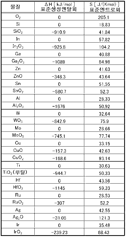

다음으로, 표 2에 나타내는 표준 생성 엔탈피ΔH 및 표준 생성 엔트로피ΔS의 값을 아래와 같은 식(1)에 대입하여, 온도가 0℃ 이상 900℃ 이하의 범위에 있어서의 각 산화 반응의 깁스 자유에너지의 값을 산출하였다. 또한, 식(1)의 T는, 온도[K]이다.Next, the values of standard production enthalpy ΔH and standard production entropy ΔS shown in Table 2 are substituted into the following equation (1), and the Gibbs free energy of each oxidation reaction in the range of 0 ° C to 900 ° C is shown. The value was calculated. In addition, T of Formula (1) is temperature [K].
![]()
![]()
도 9는, 온도가 0℃ 이상 900℃ 이하의 범위에 있어서의 각종 금속의 산화 반응의 깁스 자유에너지를 계산한 결과이다. 횡축은, 온도[℃]이며, 종축은, 깁스 자유에너지ΔG[kJ/mol]이다.9 is a result of calculating the Gibbs free energy of the oxidation reaction of various metals in the temperature range of 0 degreeC or more and 900 degrees C or less. The horizontal axis is temperature [° C.], and the vertical axis is Gibbs free energy ΔG [kJ / mol].
도 9에 나타내는 그래프로부터, 도 9의 하측에 있는 반응일수록 산화 반응이 일어나기 쉬운, 즉 산화하기 쉬운 금속이며, 도 9의 상측에 있는 반응일수록 환원 반응이 일어나기 쉬운, 즉 환원하기 쉬운 금속 산화물인 것을 알 수 있다. 따라서, 산화물 반도체막(403)에 포함되는 금속 원소보다도 내산화성을 갖는 금속은, 도 9의 상측에 있는 금속이면 좋다.From the graph shown in FIG. 9, the lower the reaction in FIG. 9, the easier the oxidation reaction occurs, that is, the more easily oxidized, and the higher the reaction in the upper side of FIG. Able to know. Therefore, the metal which has oxidation resistance rather than the metal element contained in the
예를 들면, 산화물 반도체막(403)이 In-Ga-Zn계 산화물인 경우, 인듐, 갈륨, 아연보다 내산화성을 갖는(적어도 인듐, 갈륨, 및 아연의 산화 반응의 깁스 자유에너지보다 높은) 금속이면 좋은 것을 알 수 있다. 또한, 산화물 반도체막(403)이 In-Sn-Zn계 산화물인 경우는, 인듐, 주석, 아연보다 내산화성을 갖는(적어도 인듐, 주석, 및 아연의 산화 반응의 깁스 자유에너지보다 높은) 금속이면 좋다.For example, when the
그렇지만, 인듐 등보다 내산화성을 갖는 금속인 텅스텐이나 몰리브덴이라도, 가열 처리의 온도가 높아지면, 텅스텐막이나 몰리브덴막 중에 산소가 확산해버리는 경우가 있다. 이에 의하여, 텅스텐막이나 몰리브덴막 중에 고저항 성분이 형성되어 트랜지스터의 온 전류가 저감해 버린다고 하는 문제가 생긴다. 그 때문에, 금속막(406a, 406b)으로서는, 몰리브덴보다 내산화성을 갖는(몰리브덴의 산화 반응의 깁스 자유에너지보다 높은) 금속을 이용하는 것이 보다 바람직하다. 구체적으로는, 도 9에 나타내는 바와 같이, 동, 은, 루테늄, 이리듐 등을 들 수 있다.However, even if tungsten or molybdenum, which is a metal having a higher oxidation resistance than indium or the like, oxygen may diffuse into the tungsten film or molybdenum film when the temperature of the heat treatment is increased. As a result, a problem arises in that a high resistance component is formed in the tungsten film or the molybdenum film, thereby reducing the on current of the transistor. Therefore, as the
금속막(406a, 406b)으로서 동, 은, 루테늄, 이리듐 등을 이용함에 의해, 산화물 반도체막(403)으로부터 산소를 뽑아내는 것을 방지할 수가 있기 때문에, 산화물 반도체막(403)의 산소 결손이 증대하는 것을 억제하여, 트랜지스터(410)의 스레숄드 전압이 마이너스 방향으로 시프트하는 것을 억제할 수가 있다.By using copper, silver, ruthenium, iridium, or the like as the
또한, 금속막(406a, 406b)은, 산화되기 어렵고, 금속막(406a, 406b) 중에 산소가 확산하는 것을 억제할 수 있기 때문에, 금속막(406a, 406b) 중에 고저항 성분이 형성되는 것을 억제할 수가 있다. 따라서, 산화물 반도체막(403), 소스 전극층(407a), 및 드레인 전극층(407b)에 기인하는 저항을 저감할 수가 있기 때문에, 트랜지스터(410)의 온 전류의 저하를 억제할 수가 있다.In addition, since the
또한, 산화물 반도체막(403)의 전자 친화력에 대하여, ±0.2 eV의 일함수를 갖는 금속막(406a, 406b)(예를 들면, 동, 은, 루테늄 등)을 선택함으로써, 산화물 반도체막(403)과 소스 전극층(407a) 및 드레인 전극층(407b)의 컨택트 저항을 저감할 수가 있기 때문에 바람직하다. 이에 의해서도, 산화물 반도체막(403), 소스 전극층(407a), 및 드레인 전극층(407b)에 기인하는 저항을 저감할 수가 있기 때문에, 트랜지스터의 온 전류의 저하를 억제할 수가 있다.In addition, the
예를 들면, In-Ga-Zn계 산화물 반도체의 전자 친화력이 4.6[eV]인 경우는, 일함수가 4.71[eV]의 루테늄을 이용하는 것이 바람직하다. 이러한 재료를, 산화물 반도체막(403), 금속막(406a, 406b)으로서 이용함에 의해, 컨택트 저항을 저감할 수가 있다.For example, when the electron affinity of an In—Ga—Zn oxide semiconductor is 4.6 [eV], ruthenium having a work function of 4.71 [eV] is preferably used. By using such a material as the
아래에, 도 9에 나타내는 금속의 산화 반응의 깁스 자유에너지가 높은 순서로 금속을 열기한다.Below, metals are opened in the order of high Gibbs free energy of the metal oxidation reaction shown in FIG.
Au, Pt, Ag, Ir, Ru, Cu, Mo, W, Sn, In, Zn, Ga, Si, Ti, Al, HfAu, Pt, Ag, Ir, Ru, Cu, Mo, W, Sn, In, Zn, Ga, Si, Ti, Al, Hf
또한, 금속막(406a, 406b)과 적층하여 마련되는 도전막(405a, 405b)은, 금속막(406a, 406b)과의 계면에서 산화물막이 형성되지 않는 재료인 것이 바람직하다. 도전막(405a, 405b)에 이용할 수가 있는 재료로서는, 금속막(406a, 406b)에 이용할 수가 있는 재료에 추가하여, 금, 백금, 티타늄, 텅스텐, 질화 티타늄, 질화 몰리브덴, 질화 텅스텐, 질화 탄탈륨 등을 들 수 있다. 도전막(405a, 405b)은 단층 구조 또는 적층 구조로 구성된다. 적층 구조인 경우, 예를 들면, 질화 탄탈륨막과 텅스텐막으로 구성할 수가 있다.The
도 1(A), 도 1(B), 도 1(C)에 나타내는 트랜지스터(410)에서는, 소스 전극층(407a) 및 드레인 전극층(407b)은, 금속막(406a, 406b)과 도전막(405a, 405b)이 동일한 재료로 되도록 구성되었을 경우에 대하여 나타내고 있다. 그 때문에, 금속막(406a, 406b)과 도전막(405a, 405b)의 계면을 점선으로 나타내고 있다. 도 1에 나타내는 트랜지스터(410)인 경우, 예를 들면, 금속막(406a, 406b)으로서 루테늄을 이용하고, 도전막(405a, 405b)으로서 루테늄을 이용할 수가 있다.In the
트랜지스터(410)에 있어서, 금속막(406a, 406b) 중에, 일부에 금속 산화물이 형성되어 있어도 좋다. 예를 들면, 금속막(406a, 406b)이 루테늄인 경우, 일부에 산화 루테늄이 형성되어 있어도 괜찮다. 금속막의 일부에 산화 루테늄이 형성되어 있었다고 하더라도, 산화 루테늄의 저항율은 3.5×10⁻⁵[cmΩ](300 K)이며, 소스 전극층 및 드레인 전극층에 고저항 성분은 형성되지 않기 때문에 바람직하다.In the
또한, 산화물 반도체막(403)은, 에너지갭이 2.8 eV 내지 3.2 eV이며, 실리콘의 에너지갭 1.1 eV와 비교하여 크다. 또한, 산화물 반도체막(403)의 소수 캐리어는, 10-9cm-3이며, 실리콘의 진성 캐리어 밀도의 1011 cm-3과 비교하여 극히 작다.The
산화물 반도체막(403)의 다수 캐리어(전자)는, 트랜지스터의 소스로부터 흐를 뿐이다. 또한, 채널 형성 영역을 완전 공핍화하는 것이 가능하기 때문에, 트랜지스터의 오프 전류를 극히 작게 하는 것이 가능하다. 산화물 반도체막(403)을 이용한 트랜지스터의 오프 전류는, 실온에서, 10 yA/m 이하, 85℃~95℃에서도, 1 zA/m 이하가 되어, 극히 작다.The majority carriers (electrons) of the
따라서, 산화물 반도체막(403)을 이용한 트랜지스터는, S값이 작아져, 이상적인 값을 얻을 수 있다. 또한, 해당 트랜지스터는 신뢰성이 높다.Therefore, the transistor using the
다음으로, 도 1에 나타내는 트랜지스터(410)와 일부 다른 트랜지스터에 대하여, 도 2를 참조하여 설명한다.Next, the
도 2(A)는, 트랜지스터(420)의 평면도이며, 도 2(B)는, 도 2(A)의 C1-C2에 있어서의 단면도(채널길이 방향의 단면도)다. 또한, 도 2(A)에서는, 번잡하게 되는 것을 피하기 위해, 트랜지스터(420)의 구성요소의 일부(예를 들면, 게이트 절연막(402) 등)를 생략하여 도시하고 있다.FIG. 2A is a plan view of the
도 2(A), 도 2(B)에 나타내는 트랜지스터(420)에 있어서, 소스 전극층(417a) 및 드레인 전극층(417b)은, 금속막(406a, 406b)과 도전막(415a, 415b)이 서로 다른 재료가 되도록 구성되어 있다. 그 때문에, 금속막(406a, 406b)과 도전막(415a, 415b)의 계면을 실선으로 나타내고 있다. 또한, 도전막(415a, 415b)은, 도전막(405a, 405b)과 동일 재료를 이용하여, 단층 구조 또는 적층 구조로 구성된다. 도 2에 나타내는 트랜지스터(420)의 경우, 예를 들면, 금속막(406a, 406b)으로서 루테늄을 이용하고, 도전막(415a, 415b)으로서 질화 탄탈륨을 이용할 수가 있다.In the
또한, 트랜지스터(420)에 있어서, 소스 전극층(417a) 및 드레인 전극층(417b)의 구성 이외는, 트랜지스터(410)와 같기 때문에, 트랜지스터(410)에 관한 기재를 참조할 수 있다.Note that, in the
이상 설명한 바와 같이, 산화물 반도체막(403)에 접하는 금속막(406a, 406b)으로서 산화물 반도체막(403)에 포함되는 금속 원소보다도 내산화성을 갖는(적어도 인듐, 갈륨, 아연, 및 주석의 산화 반응의 깁스 자유에너지보다 높은) 금속을 이용함에 의해, 산화물 반도체막(403)으로부터 산소를 뽑아내는 것을 방지할 수가 있다. 이에 의하여, 소스 전극층(417a) 및 드레인 전극층(417b)과 산화물 반도체막(403)의 계면에 있어서의 산소 결손이 증대하는 것을 억제하여, 트랜지스터의 스레숄드 전압이 마이너스 방향으로 시프트하는 것을 억제할 수가 있다.As described above, the
또한, 금속막(406a, 406b)은, 산화물 반도체막(403)보다도 산화하기 어렵고, 금속막(406a, 406b) 중에 산소가 확산하는 것을 억제할 수 있기 때문에, 금속막(406a, 406b) 중에 고저항 성분이 형성되는 것을 억제할 수가 있다. 따라서, 산화물 반도체막, 소스 전극층, 및 드레인 전극층에 기인하는 저항을 저감할 수가 있기 때문에, 트랜지스터의 온 전류의 저하를 억제할 수가 있다.In addition, since the
본 실시형태에 나타내는 구성, 방법 등은, 다른 실시형태에 나타내는 구성, 방법 등과 적절히 조합하여 이용할 수가 있다.The structure, method, etc. which are shown in this embodiment can be used in appropriate combination with the structure, method, etc. which are shown in another embodiment.
(실시형태 2)(Embodiment 2)
본 실시형태에서는, 도 1에 나타내는 트랜지스터(410)를 갖는 반도체 장치의 제작 방법의 일 예에 대하여, 도 3을 참조하여 설명한다.In this embodiment, an example of the manufacturing method of the semiconductor device which has the
절연 표면을 갖는 기판(400)에 사용할 수가 있는 기판에 큰 제한은 없지만, 적어도, 나중의 가열 처리에 견딜 수 있는 정도의 내열성을 갖는 것이 필요하다. 예를 들면, 바륨보로실리케이트 유리나 알루미노보로실리케이트 유리 등의 유리 기판, 세라믹 기판, 석영 기판, 사파이어 기판 등을 이용할 수가 있다. 또한, 실리콘이나 탄화 실리콘 등의 단결정 반도체 기판, 다결정 반도체 기판, 실리콘 게르마늄 등의 화합물 반도체 기판, SOI 기판 등을 적용할 수도 있으며, 이러한 기판상에 반도체 소자가 마련된 것을, 기판(400)으로서 이용하여도 좋다.Although there is no big restriction | limiting in the board | substrate which can be used for the board |
또한, 기판(400)으로서 가요성 기판을 이용하여 반도체 장치를 제작하여도 괜찮다. 가요성을 갖는 반도체 장치를 제작하려면, 가요성 기판상에 산화물 반도체막(403)을 포함한 트랜지스터(410)를 직접 제작하여도 괜찮고, 다른 제작 기판에 산화물 반도체막(403)을 포함한 트랜지스터(410)를 제작하고, 그 후, 가요성 기판에 박리, 전치(轉置)하여도 괜찮다. 또한, 제작 기판으로부터 가요성 기판에 박리, 전치하기 위해서, 제작 기판과 산화물 반도체막(403)을 포함한 트랜지스터(410)의 사이에 박리층을 마련하면 좋다.In addition, you may manufacture a semiconductor device using the flexible substrate as the board |
다음으로, 기판(400) 상에, 기초막으로서 기능하는 절연막을 형성하여도 좋다. 절연막으로서는, 플라즈마 CVD법 또는 스퍼터링법에 의하여, 산화 실리콘, 산화 질화 실리콘, 산화 알루미늄, 산화 질화 알루미늄, 산화 하프늄, 산화 갈륨 등의 산화물 절연막, 질화 실리콘, 산화 질화 실리콘, 질화 알루미늄, 질화 산화 알루미늄 등의 질화물 절연막, 또는 이러한 혼합 재료를 이용하여 형성할 수가 있다. 절연막으로서 예를 들면, 질화 실리콘막과 산화 질화 실리콘막의 적층 구조를 이용함에 의해, 기판으로부터 금속이나 수소 등이, 나중에 형성되는 산화물 반도체막에 침입하는 것을 억제할 수 있기 때문에 바람직하다.Next, an insulating film that functions as a base film may be formed on the
기초막으로서 기능하는 절연막(적층 구조인 경우는, 산화물 반도체막(403)과 접하는 막)의 막 중(벌크 중)에는, 적어도 화학량론적 조성을 넘는 양의 산소가 존재하는 것이 바람직하다. 예를 들면, 절연막으로서 산화 실리콘막을 이용하는 경우에는, 산소의 양을 SiO2 +α(다만, α>0)로 하는 것이 바람직하다.In the film (in the bulk) of the insulating film (the film in contact with the
산소의 공급원이 되는 산소를 많이(과잉으로) 포함한 절연막을 산화물 반도체막(403)과 접하여 마련함에 의해, 절연막으로부터 산화물 반도체막(403)에 산소를 공급할 수가 있다. 또한, 산화물 반도체막(403)과 절연막의 적어도 일부가 접한 상태에서 가열 처리를 실시함에 의해 산화물 반도체막(403)으로의 산소의 공급을 실시하여도 괜찮다. 산소를 많이 포함한 절연막을 이용함에 의해, 산화물 반도체막(403)에 산소를 공급할 수가 있기 때문에, 산화물 반도체막(403)의 산소 결손을 저감할 수가 있다.By providing an insulating film containing a large amount (excess) of oxygen as a source of oxygen in contact with the
다음으로, 기판(400) 상에, 게이트 전극층(이와 동일한 층에서 형성되는 배선을 포함한다)이 되는 도전막을 형성한다. 도전막의 재료는, 몰리브덴, 티타늄, 탄탈륨, 텅스텐, 알루미늄, 동, 크롬, 네오디뮴, 스칸듐 등의 금속재료 또는 이들을 주성분으로 하는 합금 재료를 이용하여 형성할 수가 있다. 도전막은 단층 구조 또는 적층 구조로 성막된다.Next, a conductive film serving as a gate electrode layer (including a wiring formed from the same layer) is formed on the
또한, 도전막의 재료는, 산화 인듐 주석, 산화 텅스텐을 포함한 인듐 산화물, 산화 텅스텐을 포함한 인듐 아연 산화물, 산화 티타늄을 포함한 인듐 산화물, 산화 티타늄을 포함한 인듐 주석 산화물, 산화 인듐 산화 아연, 산화 규소를 첨가한 인듐 주석 산화물 등의 도전성 재료를 적용할 수도 있다. 또한, 상기 도전성 재료와 상기 금속재료의 적층 구조로 할 수도 있다.In addition, the material of the conductive film includes indium tin oxide, indium oxide containing tungsten oxide, indium zinc oxide containing tungsten oxide, indium oxide containing titanium oxide, indium tin oxide containing titanium oxide, indium zinc oxide and silicon oxide. Conductive materials, such as indium tin oxide, can also be applied. Moreover, it can also be set as the laminated structure of the said electroconductive material and the said metal material.
또한, 나중에 형성되는 게이트 절연막(402)과 접하는 도전막으로서, 질소를 포함한 금속 산화물, 구체적으로는, 질소를 포함한 In-Ga-Zn-O막이나, 질소를 포함한 In-Sn-O막이나, 질소를 포함한 In-Ga-O막이나, 질소를 포함한 In-Zn-O막이나, 질소를 포함한 Sn-O막이나, 질소를 포함한 In-O막이나, 금속 질화막(InN, SnN 등)을 이용할 수가 있다. 이러한 막은, 5 eV(전자 볼트), 바람직하게는 5.5 eV(전자 볼트) 이상의 일함수를 가지기 때문에, 게이트 전극층으로서 이용하였을 경우, 트랜지스터의 전기 특성의 스레숄드 전압을 플러스로 할 수 있어 소위 노멀리 오프(normally off)의 스위칭 소자를 실현할 수 있다.Further, as a conductive film in contact with the
다음으로, 포토리소그라피 공정에 의해 도전막상에 레지스트 마스크를 형성하고, 선택적으로 에칭을 실시하여 게이트 전극층(401)을 형성한다. 게이트 전극층(401)을 형성한 후, 레지스트 마스크를 제거한다. 도전막의 에칭은, 건식 에칭이라도, 습식 에칭이라도 좋고, 양쪽 모두를 이용하여도 괜찮다.Next, a resist mask is formed on the conductive film by a photolithography process, and is selectively etched to form the
또한, 게이트 전극층(401) 형성 후에, 기판(400), 및 게이트 전극층(401)에 가열 처리를 실시하여도 괜찮다. 예를 들면, GRTA 장치에 의하여, 650℃, 1분 ~ 5분간, 가열 처리를 실시하면 좋다. 또한, 전기로에 의하여, 500℃, 30분 ~ 1시간, 가열 처리를 실시하여도 괜찮다. 가열 처리를 실시함으로써, 기판(400)이나 게이트 전극층(401)에 포함되는 수소나 물 등을 제거할 수가 있다.After the
다음으로, 게이트 전극층(401) 상에 게이트 절연막(402)을 형성한다.Next, a
또한, 게이트 절연막(402)의 피복성을 향상시키기 위해서, 게이트 전극층(401) 표면에 평탄화 처리를 실시하여도 괜찮다. 특히, 게이트 절연막(402)으로서 막두께가 얇은 절연막을 이용하는 경우, 게이트 전극층(401) 표면의 평탄성이 양호한 것이 바람직하다.In addition, in order to improve the coating | cover property of the
게이트 절연막(402)의 막두께는, 1 nm 이상 20 nm 이하로 하고, 스퍼터링법, MBE법, CVD법, PECVD법, 펄스 레이저 퇴적법, ALD법 등을 적절히 이용할 수가 있다. 또한, 게이트 절연막(402)은, 스퍼터링 타겟 표면에 대하여, 대략 수직하게 복수의 기판 표면이 세트된 상태에서 성막을 실시하는 스퍼터 장치를 이용하여 성막하여도 괜찮다.The film thickness of the
게이트 절연막(402)의 재료로서는, 산화 실리콘, 산화 갈륨, 산화 알루미늄, 질화 실리콘, 산화 질화 실리콘, 산화 질화 알루미늄, 또는 질화 산화 실리콘을 이용하여 형성할 수가 있다. 또한, 게이트 절연막(402)의 재료로서 산화 하프늄, 산화 이트륨, 하프늄 실리케이트(HfSixOy (x>0, y>0)), 질소가 첨가된 하프늄 실리케이트(HfSiOxNy (x>0, y>0)), 하프늄 알루미네이트(HfAlxOy (x>0, y>0)), 산화 란타늄 등의 high-k재료를 이용함으로써 게이트 리크 전류를 저감할 수 있다. 또한, 게이트 절연막(402)은, 상기 재료를 이용하여, 단층 구조 또는 적층 구조로 형성할 수가 있다.As the material of the
게이트 절연막(402)은, 나중에 형성되는 산화물 반도체막(403)과 접하는 부분에 있어서 산소를 포함하는 것이 바람직하다. 특히, 게이트 절연막(402)은, 막 중(벌크 중)에 적어도 화학량론비를 넘는 양의 산소가 존재하는 것이 바람직하며, 예를 들면, 게이트 절연막(402)으로서 산화 실리콘막을 이용하는 경우에는, SiO2 +α(다만, α>0)로 한다.It is preferable that the
산소의 공급원이 되는 산소를 많이(과잉으로) 포함한 게이트 절연막(402)을, 나중에 형성되는 산화물 반도체막(403)과 접하여 마련함에 의해, 그 게이트 절연막(402)으로부터 산화물 반도체막(403)에 산소를 공급할 수가 있다. 또한, 산화물 반도체막(403)과 게이트 절연막(402)이 적어도 일부가 접한 상태에서 가열 처리를 실시함에 의해, 게이트 절연막(402)으로부터 산화물 반도체막(403)으로의 산소의 공급을 실시하여도 괜찮다.The
산화물 반도체막(403)에 산소를 공급함에 의하여, 산화물 반도체막(403) 중의 산소 결손을 저감할 수가 있다. 게다가 게이트 절연막(402)은, 제작하는 트랜지스터의 사이즈나 게이트 절연막(402)의 단차 피복성을 고려하여 형성하는 것이 바람직하다.By supplying oxygen to the
또한, 게이트 절연막(402) 형성 후에, 기판(400), 게이트 전극층(401), 및 게이트 절연막(402)에 가열 처리를 실시하여도 괜찮다. 예를 들면, GRTA 장치에 의하여, 650℃, 1분 ~ 5분간, 가열 처리를 실시하면 좋다. 또한, 전기로에 의하여, 500℃, 30분 ~ 1시간, 가열 처리를 실시하여도 괜찮다. 가열 처리를 실시함으로써, 게이트 절연막(402)에 포함되는 수소나 물 등을 제거할 수가 있다.After the
다음으로, 게이트 절연막(402) 상에 산화물 반도체막을 형성한다. 그 후, 포토리소그라피 공정에 의해 산화물 반도체막상에 레지스트 마스크를 형성하고, 선택적으로 에칭을 실시하여 섬형상의 산화물 반도체막(403)을 형성한다(도 3(A) 참조). 산화물 반도체막(403)을 형성한 후, 레지스트 마스크를 제거한다. 산화물 반도체막(403)의 에칭은, 건식 에칭이라도, 습식 에칭이라도 좋고, 양쪽 모두를 이용하여도 괜찮다.Next, an oxide semiconductor film is formed on the
또한, 섬형상의 산화물 반도체막(403)을 형성하기 위한 레지스트 마스크를 잉크젯법으로 형성하여도 좋다. 레지스트 마스크를 잉크젯법으로 형성하면, 포토마스크를 사용하지 않기 때문에, 제조 비용을 저감할 수 있다.Further, a resist mask for forming the island-shaped
또한, 산화물 반도체막의 에칭은, 건식 에칭이라도, 습식 에칭이라도 좋고, 양쪽 모두를 이용하여도 괜찮다. 예를 들면, 산화물 반도체막의 습식 에칭에 이용하는 에칭액으로서는, 인산과 초산과 초산을 혼합한 용액 등을 이용할 수가 있다. 또한, ITO-07N(관동화학사 제품)를 이용하여도 괜찮다. 또한, ICP(InductiVely Coupled Plasma:유도 결합형 플라즈마) 에칭법에 따른 건식 에칭에 의해 에칭 가공하여도 괜찮다.The etching of the oxide semiconductor film may be either dry etching or wet etching, or both may be used. For example, a solution obtained by mixing phosphoric acid, acetic acid, and acetic acid can be used as the etching solution used for the wet etching of the oxide semiconductor film. In addition, you may use ITO-07N (made by Kanto Chemical). In addition, you may etch by dry etching by the ICP (InductiVely Coupled Plasma) etching method.
산화물 반도체막(403)에 이용하는 산화물 반도체로서는, 적어도 인듐(In)을 포함한다. 특히, 인듐(In)과 아연(Zn)을 포함하는 것이 바람직하다. 또한, 그 산화물 반도체막을 이용한 트랜지스터의 전기 특성의 격차를 줄이기 위한 스태빌라이저로서, 그들에 부가하여 갈륨(Ga)을 갖는 것이 바람직하다. 또한, 스태빌라이저로서 주석(Sn), 하프늄(Hf), 알루미늄(Al), 지르코늄(Zr) 중의 어느 일종 또는 복수종을 갖는 것이 바람직하다.The oxide semiconductor used for the
또한, 다른 스태빌라이저로서 란타노이드인, 란타늄(La), 세륨(Ce), 프라세오디뮴(Pr), 네오디뮴(Nd), 사마륨(Sm), 유로퓸(Eu), 가돌리늄(Gd), 테르븀(Tb), 디스프로슘(Dy), 홀뮴(Ho), 에르븀(Er), 툴륨(Tm), 이테르븀(Yb), 루테튬(Lu) 중의 어느 일종 혹은 복수종을 가져도 괜찮다.In addition, as other stabilizers, lanthanoids, lanthanum (La), cerium (Ce), praseodymium (Pr), neodymium (Nd), samarium (Sm), europium (Eu), gadolinium (Gd), terbium (Tb), and dysprosium You may have any kind or multiple types of (Dy), holmium (Ho), erbium (Er), thulium (Tm), ytterbium (Yb), and lutetium (Lu).
예를 들면, 산화물 반도체로서, 산화 인듐, 산화 주석, 산화 아연, 2원계 금속의 산화물인 In-Zn계 산화물, In-Mg계 산화물, In-Ga계 산화물, 3원계 금속의 산화물인 In-Ga-Zn계 산화물(IGZO라고도 표기한다), In-Al-Zn계 산화물, In-Sn-Zn계 산화물, In-Hf-Zn계 산화물, In-La-Zn계 산화물, In-Ce-Zn계 산화물, In-Pr-Zn계 산화물, In-Nd-Zn계 산화물, In-Sm-Zn계 산화물, In-Eu-Zn계 산화물, In-Gd-Zn계 산화물, In-Tb-Zn계 산화물, In-Dy-Zn계 산화물, In-Ho-Zn계 산화물, In-Er-Zn계 산화물, In-Tm-Zn계 산화물, In-Yb-Zn계 산화물, In-Lu-Zn계 산화물, 4원계 금속의 산화물인 In-Sn-Ga-Zn계 산화물, In-Hf-Ga-Zn계 산화물, In-Al-Ga-Zn계 산화물, In-Sn-Al-Zn계 산화물, In-Sn-Hf-Zn계 산화물, In-Hf-Al-Zn계 산화물을 이용할 수가 있다.For example, as an oxide semiconductor, In-Ga which is an oxide of indium oxide, tin oxide, zinc oxide, or an oxide of a binary metal, an In-Zn oxide, an In-Mg oxide, an In-Ga oxide, or an oxide of a ternary metal is used. -Zn oxide (also referred to as IGZO), In-Al-Zn oxide, In-Sn-Zn oxide, In-Hf-Zn oxide, In-La-Zn oxide, In-Ce-Zn oxide , In-Pr-Zn oxide, In-Nd-Zn oxide, In-Sm-Zn oxide, In-Eu-Zn oxide, In-Gd-Zn oxide, In-Tb-Zn oxide, In -Dy-Zn oxide, In-Ho-Zn oxide, In-Er-Zn oxide, In-Tm-Zn oxide, In-Yb-Zn oxide, In-Lu-Zn oxide, quaternary metal In—Sn—Ga—Zn oxides, In—Hf—Ga—Zn oxides, In—Al—Ga—Zn oxides, In—Sn—Al—Zn oxides, In—Sn—Hf—Zn oxides Oxides and In-Hf-Al-Zn oxides can be used.
예를 들면, In-Ga-Zn계 산화물이란, In와 Ga와 Zn를 주성분으로서 갖는 산화물이라는 의미이며, In와 Ga와 Zn의 비율은 묻지 않는다. 또한, In와 Ga와 Zn 이외의 금속 원소가 들어가 있어도 괜찮다.For example, an In—Ga—Zn-based oxide means an oxide having In, Ga, and Zn as main components, and the ratio of In, Ga, and Zn does not matter. Moreover, metal elements other than In, Ga, and Zn may be contained.
또한, 산화물 반도체로서 InMO3(ZnO)m (m>0, 또한, m은 정수가 아니다)로 표기되는 재료를 이용하여도 괜찮다. 또한, M은, Ga, Fe, Mn 및 Co로부터 선택된 하나의 금속 원소 또는 복수의 금속 원소를 나타낸다. 또한, 산화물 반도체로서 In2SnO5(ZnO)n (n>0, 또한, n은 정수)로 표기되는 재료를 이용하여도 괜찮다.As the oxide semiconductor, a material denoted by InMO 3 (ZnO) m (m> 0, where m is not an integer) may be used. Further, M represents one metal element or a plurality of metal elements selected from Ga, Fe, Mn and Co. As the oxide semiconductor, a material denoted by In 2 SnO 5 (ZnO) n (n> 0, and n is an integer) may be used.
예를 들면, In:Ga:Zn=1:1:1(=1/3:1/3:1/3), In:Ga:Zn=2:2:1(=2/5:2/5:1/5), 혹은 In:Ga:Zn=3:1:2(=1/2:1/6:1/3)의 원자수비의 In-Ga-Zn계 산화물이나 그 조성 근방의 산화물을 이용할 수가 있다. 혹은, In:Sn:Zn=1:1:1(=1/3:1/3:1/3), In:Sn:Zn=2:1:3(=1/3:1/6:1/2) 혹은 In:Sn:Zn=2:1:5(=1/4:1/8:5/8)의 원자수비의 In-Sn-Zn계 산화물이나 그 조성 근방의 산화물을 이용하면 좋다.For example, In: Ga: Zn = 1: 1: 1 (= 1/3: 1/3: 1/3), In: Ga: Zn = 2: 2: 1 (= 2/5: 2/5 : 1/5) or In-Ga-Zn-based oxides having an atomic ratio of In: Ga: Zn = 3: 1: 2 (= 1/2: 1/6: 1/3) and oxides in the vicinity of the composition It is available. Or In: Sn: Zn = 1: 1: 1 (= 1/3: 1/3: 1/3), In: Sn: Zn = 2: 1: 3 (= 1/3: 1/6: 1 / 2) or an In-Sn-Zn-based oxide having an atomic ratio of In: Sn: Zn = 2: 1: 5 (= 1/4: 1/8: 5/8) or an oxide near its composition may be used. .
그러나, 인듐을 포함한 산화물 반도체는, 이들에 한정되지 않고, 필요로 하는 반도체 특성(이동도, 스레숄드, 격차 등)에 따라서 적절한 조성의 것을 이용하면 좋다. 또한, 필요로 하는 반도체 특성을 얻기 위해서, 캐리어 농도나 불순물 농도, 결함 밀도, 금속 원소와 산소의 원자수비, 원자간 거리, 밀도 등을 적절한 것으로 하는 것이 바람직하다.However, the oxide semiconductor containing indium is not limited to these, and one having an appropriate composition may be used in accordance with required semiconductor characteristics (mobility, threshold, gap, etc.). Moreover, in order to acquire the required semiconductor characteristic, it is preferable to make carrier density | concentration, impurity concentration, defect density, atomic ratio of a metal element and oxygen, interatomic distance, density, etc. into an appropriate thing.
예를 들면, In-Sn-Zn계 산화물에서는 비교적 용이하게 높은 이동도를 얻을 수 있다. 그렇지만, In-Ga-Zn계 산화물에서도, 벌크내 결함 밀도를 낮게 함에 의해 이동도를 올릴 수가 있다.For example, in the In—Sn—Zn-based oxide, high mobility can be obtained relatively easily. However, even in In—Ga—Zn-based oxides, the mobility can be increased by lowering the defect density in the bulk.
또한, 예를 들면, In, Ga, Zn의 원자수비가 In:Ga:Zn=a:b:c(a+b+c=1)인 산화물의 조성이, 원자수비가 In:Ga:Zn=A:B:C(A+B+C=1)인 산화물의 조성의 근방이라는 것은, a, b, c가, (a-A)2+(b-B)2+(c-C)2 ≤ r2를 만족시키는 것을 말한다. r로서는, 예를 들면, 0.05로 하면 좋다. 다른 산화물에서도 마찬가지다.For example, the composition of the oxide whose atomic ratio of In, Ga, and Zn is In: Ga: Zn = a: b: c (a + b + c = 1) has an atomic ratio of In: Ga: Zn = A: B: The vicinity of the composition of the oxide of C (A + B + C = 1) means that a, b and c satisfy (aA) 2 + (bB) 2 + (cC) 2 ≤ r 2 . As r, it is good to set it as 0.05, for example. The same is true for other oxides.
산화물 반도체막(403)은, 단결정, 다결정(폴리크리스탈이라고도 한다) 또는 비정질 등의 상태를 취한다.The
바람직하게는, 산화물 반도체막(403)은, CAAC-OS(C Axis Aligned Crystalline Oxide Semiconductor) 막으로 한다.Preferably, the
CAAC-OS막은, 완전한 단결정은 아니고, 완전한 비정질도 아니다. CAAC-OS막은, 비정질상에 결정부를 갖는 결정-비정질 혼상 구조의 산화물 반도체막이다. 또한, 해당 결정부는, 한 변이 100 nm미만의 입방체내에 들어가는 크기인 것이 많다. 또한, 투과형 전자현미경(TEM:Transmission Electron Microscope)에 의한 관찰상에서는, CAAC-OS막에 포함되는 비정질부와 결정부와의 경계는 명확하지 않다. 또한, TEM에 의해 CAAC-OS막에는 입계(그레인 바운다리라고도 한다)는 확인할 수 없다. 그 때문에, CAAC-OS막은, 입계에 기인하는 전자 이동도의 저하가 억제된다.The CAAC-OS film is not a complete single crystal, nor is it completely amorphous. The CAAC-OS film is an oxide semiconductor film having a crystal-amorphous mixed phase structure having a crystal part in an amorphous phase. In addition, the crystal part is large enough to have one side in a cube of less than 100 nm. In addition, in the observation by a transmission electron microscope (TEM), the boundary between the amorphous part and the crystal part included in the CAAC-OS film is not clear. In addition, grain boundaries (also called grain boundaries) cannot be confirmed in the CAAC-OS film by TEM. Therefore, in the CAAC-OS film, the decrease in electron mobility due to grain boundaries is suppressed.
CAAC-OS막에 포함되는 결정부는, c축이 CAAC-OS막의 피형성면의 법선 벡터 또는 표면의 법선 벡터에 평행한 방향으로 정돈되며, 또한 ab면에 수직한 방향으로부터 보아서 삼각형상 또는 육각형상의 원자 배열을 가지며, c축에 수직한 방향으로부터 보아서 금속 원자가 층상 또는 금속 원자와 산소 원자가 층상으로 배열하고 있다. 또한, 다른 결정부 사이에서, 각각 a축 및 b축의 방향이 다르더라도 괜찮다. 본 명세서에 있어서, 단지 수직이라고 기재하는 경우, 85도 이상 95도 이하의 범위도 포함되는 것으로 한다. 또한, 단지 평행이라고 기재하는 경우, -5도 이상 5도 이하의 범위도 포함되는 것으로 한다.The crystal part included in the CAAC-OS film has a c-axis arranged in a direction parallel to the normal vector of the surface to be formed of the CAAC-OS film or the normal vector of the surface, and is triangular or hexagonal as viewed from the direction perpendicular to the ab plane. It has an atomic arrangement, and the metal atoms are arranged in the layer form or the metal atoms and the oxygen atoms are layered as viewed from the direction perpendicular to the c axis. In addition, the directions of the a-axis and the b-axis may be different, respectively, between the different crystal parts. In this specification, when describing only vertical, the range of 85 degrees or more and 95 degrees or less shall also be included. In addition, when only parallel is described, the range of -5 degrees or more and 5 degrees or less shall also be included.
또한, CAAC-OS막에 있어서, 결정부의 분포가 일정하지 않아도 좋다. 예를 들면, CAAC-OS막의 형성 과정에 있어서, 산화물 반도체막의 표면측으로부터 결정 성장시키는 경우, 피형성면의 근방에 대하여 표면의 근방에서는 결정부가 차지하는 비율이 높아지는 일이 있다. 또한, CAAC-OS막에 불순물을 첨가함에 의하여, 해당 불순물 첨가 영역에 있어서 결정부가 비정질화하는 것도 있다.In addition, in the CAAC-OS film, the distribution of the crystal parts may not be constant. For example, in the process of forming the CAAC-OS film, when crystal growth is performed from the surface side of the oxide semiconductor film, the ratio of the crystal portion to the vicinity of the surface to be formed increases in the vicinity of the surface to be formed. In addition, by adding an impurity to the CAAC-OS film, the crystal part may be amorphous in the impurity addition region.
CAAC-OS막에 포함되는 결정부의 c축은, CAAC-OS막의 피형성면의 법선 벡터 또는 표면의 법선 벡터에 평행한 방향으로 정돈되기 때문에, CAAC-OS막의 형상(피형성면의 단면 형상 또는 표면의 단면 형상)에 따라서는 서로 다른 방향을 향하는 일이 있다. 또한, 결정부의 c축의 방향은, CAAC-OS막이 형성되었을 때의 피형성면의 법선 벡터 또는 표면의 법선 벡터에 평행한 방향이 된다. 결정부는, 성막함에 의하여, 또는 성막 후에 가열 처리 등의 결정화 처리를 실시함으로써 형성된다.Since the c-axis of the crystal part included in the CAAC-OS film is aligned in a direction parallel to the normal vector of the surface to be formed of the CAAC-OS film or the normal vector of the surface, the shape of the CAAC-OS film (cross-sectional shape or surface of the surface to be formed) Depending on the cross-sectional shape), they may face different directions. The c-axis direction of the crystal part is a direction parallel to the normal vector of the surface to be formed or the normal vector of the surface when the CAAC-OS film is formed. The crystal part is formed by film formation or by performing crystallization treatment such as heat treatment after film formation.
CAAC-OS막을 이용한 트랜지스터는, 가시광선이나 보라색 외광의 조사에 의한 전기 특성의 변동이 작다. 따라서, 해당 트랜지스터는 신뢰성이 높다.The transistor using the CAAC-OS film has a small variation in electrical characteristics due to irradiation with visible light or purple external light. Therefore, the transistor is highly reliable.
또한, 산화물 반도체막을 구성하는 산소의 일부는 질소로 치환되어도 괜찮다.In addition, a part of oxygen which comprises an oxide semiconductor film may be substituted by nitrogen.
또한, CAAC-OS와 같이 결정부를 갖는 산화물 반도체에서는, 보다 벌크내 결함을 저감할 수가 있으며, 표면의 평탄성을 높이면 아몰퍼스 상태의 산화물 반도체 이상의 이동도를 얻을 수 있다. 표면의 평탄성을 높이기 위해서는, 평탄한 표면상에 산화물 반도체를 형성하는 것이 바람직하며, 구체적으로는, 평균면 조도(Ra)가 1 nm 이하, 바람직하게는 0.3 nm 이하, 보다 바람직하게는 0.1 nm 이하의 표면상에 형성하면 좋다.In addition, in oxide semiconductors having crystal parts such as CAAC-OS, defects in bulk can be further reduced, and when the surface flatness is increased, mobility of oxide semiconductors in an amorphous state or more can be obtained. In order to increase the flatness of the surface, it is preferable to form an oxide semiconductor on a flat surface. Specifically, the average surface roughness Ra is 1 nm or less, preferably 0.3 nm or less, more preferably 0.1 nm or less. What is necessary is just to form on a surface.
또한, Ra란, JIS B 0601:2001(ISO4287:1997)에서 정의되어 있는 산술 평균 조도를 곡면에 대해서 적용할 수 있도록 삼차원으로 확장한 것이며, 「기준면으로부터 지정면까지의 편차의 절대치를 평균한 값」으로 표현할 수 있으며, 아래와 같이 식(2)으로 정의된다.Ra is an extension of arithmetic mean roughness defined in JIS B 0601: 2001 (ISO4287: 1997) in three dimensions so that it can be applied to curved surfaces, and "average of the absolute value of the deviation from the reference plane to the designated plane." It can be expressed as Equation (2).

여기서, 지정면이란, 조도 계측의 대상이 되는 면이며, 좌표(x1, y1, f(x1, y1))(x1, y2, f(x1, y2))(x2, y1, f(x2, y1))(x2, y2, f(x2, y2))의 4점으로 나타내어지는 사각형의 영역으로 하고, 지정면을 xy평면에 투영 한 직사각형의 면적을 S0, 기준면의 높이(지정면의 평균 높이)를 Z0로 한다. Ra는 원자간력 현미경(AFM:Atomic Force Microscope)으로 측정 가능하다.Here, the designation surface is a surface to be subjected to illuminance measurement, and coordinates (x 1 , y 1 , f (x 1 , y 1 )) (x 1 , y 2 , f (x 1 , y 2 )) (x 2 , the area of the rectangle represented by four points of y 1 , f (x 2 , y 1 )) (x 2 , y 2 , f (x 2 , y 2 )), The area is S 0 , and the height of the reference plane (average height of the designated plane) is Z 0 . Ra can be measured with an atomic force microscope (AFM).
산화물 반도체막(403) 표면의 평탄성을 높이기 위해서, 게이트 절연막(402)에 있어서, 산화물 반도체막(403)이 접하여 형성되는 영역에, 평탄화 처리를 실시하는 것이 바람직하다. 평탄화 처리로서는, 특별히 한정되지 않지만, 연마 처리(예를 들면, 화학적 기계 연마법(Chemical Mechanical Polishing:CMP)), 건식 에칭 처리, 플라즈마 처리를 이용할 수가 있다.In order to improve the flatness of the surface of the
플라즈마 처리로서는, 예를 들면, 아르곤 가스를 도입하여 플라즈마를 발생시키는 역스퍼터링을 실시할 수가 있다. 역스퍼터링이란, 아르곤 분위기하에서 기판측에 RF전원을 이용하여 전압을 인가하여 기판 근방에 플라즈마를 형성하여 표면을 개질하는 방법이다. 또한, 아르곤 분위기를 대신하여 질소, 헬륨, 산소 등을 이용하여도 괜찮다. 역스퍼터링을 실시하면, 게이트 절연막(402)의 표면에 부착되어 있는 분말상 물질(파티클, 쓰레기라고도 한다)을 제거할 수가 있다.As the plasma treatment, for example, reverse sputtering may be performed in which argon gas is introduced to generate plasma. Reverse sputtering is a method of modifying a surface by applying a voltage to the substrate side using an RF power supply in an argon atmosphere to form a plasma near the substrate. Moreover, you may use nitrogen, helium, oxygen, etc. instead of an argon atmosphere. When reverse sputtering is performed, the powdery substance (also called particles and garbage) adhering to the surface of the
평탄화 처리로서, 연마 처리, 건식 에칭 처리, 플라즈마 처리는 여러 차례 실시하여도 좋고, 그들을 조합하여 실시하여도 괜찮다. 또한, 조합하여 실시하는 경우, 공정 순서도 특별히 한정되지 않고, 게이트 절연막(402) 표면의 요철 상태에 맞추어 적절히 설정하면 좋다.As the planarization treatment, the polishing treatment, the dry etching treatment and the plasma treatment may be performed several times or may be performed in combination. In addition, when performing in combination, a process sequence is not specifically limited, either, According to the uneven state of the surface of the
산화물 반도체막(403)의 막두께는, 1 nm이상 200 nm 이하, 바람직하게는 5 nm이상 50 nm 이하로 하고, 스퍼터링법, MBE(Molecular Beam Epitaxy) 법, CVD법, 펄스 레이저 퇴적법, ALD(Atomic Layer Deposition) 법 등을 적절히 이용할 수가 있다. 또한, 산화물 반도체막(403)은, 스퍼터링 타겟 표면에 대하여, 대략 수직하게 복수의 기판 표면이 세트된 상태에서 성막을 실시하는 스퍼터 장치를 이용하여 성막하여도 괜찮다.The film thickness of the
또한, 산화물 반도체막(403)에 포함되는 수소 또는 물의 농도는, 가능한 한 낮은 것이 바람직하다. 수소 농도가 높으면 산화물 반도체에 포함되는 원소와 수소의 결합에 의하여, 수소의 일부가 도너가 되어, 캐리어인 전자가 생겨 버리기 때문이다.In addition, the concentration of hydrogen or water contained in the
따라서, 산화물 반도체막(403)의 형성 공정에 있어서, 산화물 반도체막(403)에 수소, 또는 물이 가능한 한 포함되지 않게 하기 위해서, 산화물 반도체막(403)의 성막의 사전 처리로서 스퍼터링 장치의 예비 가열실에서 게이트 절연막(402)이 형성된 기판을 예비 가열하여, 기판 및 게이트 절연막(402)에 흡착된 수소, 수분 등의 불순물을 이탈시켜, 배기하는 것이 바람직하다. 또한, 예비 가열실에 마련하는 배기 수단은 크라이오 펌프가 바람직하다.Therefore, in the formation process of the
또한, 산화물 반도체막(403)은, 성막시에 산소가 많이 포함되도록 하는 조건(예를 들면, 산소 100%의 분위기하에서 스퍼터링법에 의해 성막을 실시하는 등)으로 성막하여, 산소를 많이 포함한(바람직하게는 산화물 반도체가 결정 상태에 있어서의 화학량론적 조성에 대하여, 산소의 함유량이 과잉인 영역이 포함되어 있는) 막으로 하는 것이 바람직하다.Further, the
또한, 본 실시형태에 있어서, 산화물 반도체막(403)으로서, AC전원 장치를 갖는 스퍼터링 장치를 이용한 스퍼터링법을 이용하여 막두께 35 nm의 In-Ga-Zn계 산화물막(IGZO막)을 성막한다. 본 실시형태에 있어서, In:Ga:Zn=3:1:2의 원자비의 In-Ga-Zn계 산화물 타겟을 이용한다. 또한, 성막 조건은, 산소 및 아르곤 분위기하(산소 유량 비율 50%), 압력 0.4 Pa, 전원 전력 0.5 kW, 기판 온도 200℃로 한다.In this embodiment, an In-Ga-Zn-based oxide film (IGZO film) having a thickness of 35 nm is formed as the
산화물 반도체막(403)을 성막할 때에 이용하는 스퍼터링 가스는 수소, 물, 수산기 또는 수소화물 등의 불순물이 제거된 고순도 가스를 이용하는 것이 바람직하다.As the sputtering gas used for forming the
감압 상태로 유지된 성막실 내에 기판을 유지한다. 그리고, 성막실 내의 잔류 수분을 제거하면서 수소 및 수분이 제거된 스퍼터 가스를 도입하고, 상기 타겟을 이용하여 기판(400) 상에 산화물 반도체막(403)을 성막한다. 성막실 내의 잔류 수분을 제거하기 위해서는, 흡착형의 진공 펌프, 예를 들면, 크라이오 펌프, 이온 펌프, 티타늄 서블리메이션(sublimation) 펌프를 이용하는 것이 바람직하다. 또한, 배기 수단으로서는, 터보 분자 펌프에 콜드 트랩을 부가한 것이라도 괜찮다. 크라이오 펌프를 이용하여 배기한 성막실은, 예를 들면, 수소 원자, 물(H2O) 등 수소 원자를 포함한 화합물(보다 바람직하게는 탄소 원자를 포함한 화합물도) 등이 배기되기 때문에, 해당 성막실에서 성막한 산화물 반도체막(403)에 포함되는 수소, 물, 수산기 또는 수소화물 등의 불순물의 농도를 저감할 수 있다.The substrate is held in the deposition chamber maintained at a reduced pressure. Then, a sputter gas from which hydrogen and moisture have been removed is introduced while removing residual moisture in the deposition chamber, and an
또한, 게이트 절연막(402)을 대기로 방출하지 않고 게이트 절연막(402)과 산화물 반도체막(403)을 연속적으로 형성하는 것이 바람직하다. 게이트 절연막(402)을 대기에 노출시키지 않고 게이트 절연막(402)과 산화물 반도체막(403)을 연속하여 형성하면, 게이트 절연막(402) 표면에 수소나 수분 등의 불순물이 흡착하는 것을 방지할 수가 있다.In addition, it is preferable to form the
또한, 산화물 반도체막(403)에, 과잉의 수소(물이나 수산기를 포함한다)를 제거(탈수화 또는 탈수소화)하기 위한 가열 처리를 실시하여도 괜찮다. 가열 처리의 온도는, 300℃ 이상 700℃ 이하, 또는 기판의 왜곡점 미만으로 한다. 가열 처리는 감압하 또는 질소 분위기하 등에서 실시할 수가 있다.In addition, the
또한, 산화물 반도체막(403)으로서 결정성 산화물 반도체막을 이용하는 경우, 결정화를 위한 가열 처리를 실시하여도 괜찮다.In addition, when using a crystalline oxide semiconductor film as the
본 실시형태에서는, 가열 처리 장치의 하나인 전기로에 기판을 도입하고, 산화물 반도체막(403)에 대해서 질소 분위기하 450℃에서 1시간, 게다가 질소 및 산소 분위기하 450℃에서 1시간의 가열 처리를 실시한다.In this embodiment, a substrate is introduced into an electric furnace which is one of the heat treatment apparatuses, and the
또한, 가열 처리 장치는 전기로에 한정되지 않고, 저항 발열체 등의 발열체로부터의 열전도 또는 열복사에 의하여, 피처리물을 가열하는 장치를 이용하여도 괜찮다. 예를 들면, LRTA(Lamp Rapid Thermal Anneal) 장치, GRTA(Gas Rapid Thermal Anneal) 장치 등의 RTA(Rapid Thermal Anneal) 장치를 이용할 수가 있다. LRTA 장치는, 할로겐 램프, 메탈할라이드 램프, 크세논 아크 램프, 카본 아크 램프, 고압 나트륨 램프, 고압 수은 램프 등의 램프로부터 발하는 광(전자파)의 복사에 의하여 피처리물을 가열하는 장치다. GRTA 장치는, 고온의 가스를 이용하여 가열 처리를 실시하는 장치다. 고온의 가스에는, 아르곤 등의 희가스, 또는 질소와 같은, 가열 처리에 의해 피처리물과 반응하지 않는 불활성 기체가 이용된다.In addition, the heat processing apparatus is not limited to an electric furnace, You may use the apparatus which heats a to-be-processed object by heat conduction or heat radiation from a heat generating body, such as a resistance heating element. For example, a Rapid Thermal Anneal (RTA) device such as a Lamp Rapid Thermal Anneal (LRTA) device or a Gas Rapid Thermal Anneal (GRTA) device can be used. The LRTA apparatus is an apparatus for heating a workpiece by radiation of light (electromagnetic waves) emitted from a lamp such as a halogen lamp, a metal halide lamp, a xenon arc lamp, a carbon arc lamp, a high pressure sodium lamp, or a high pressure mercury lamp. A GRTA apparatus is an apparatus which heat-processes using high temperature gas. As the hot gas, a rare gas such as argon or an inert gas such as nitrogen, which does not react with the object to be processed by heat treatment is used.
예를 들면, 가열 처리로서, 650℃~700℃의 고온으로 가열한 불활성 가스 중에 기판을 넣어 몇 분간 가열한 후, 기판을 불활성 가스 중에서 꺼내는 GRTA를 실시하여도 괜찮다.For example, you may perform GRTA which takes out a board | substrate in an inert gas, after putting a board | substrate in an inert gas heated at 650 degreeC-700 degreeC high temperature for several minutes as a heat processing.
또한, 가열 처리에 있어서는, 질소, 또는 헬륨, 네온, 아르곤 등의 희가스에, 물, 수소 등이 포함되지 않는 것이 바람직하다. 또는, 열처리 장치에 도입하는 질소, 또는 헬륨, 네온, 아르곤 등의 희가스의 순도를, 6 N(99.9999%) 이상 바람직하게는 7 N(99.99999%) 이상(즉 불순물 농도를 1 ppm 이하, 바람직하게는 0.1 ppm 이하)으로 하는 것이 바람직하다.Moreover, in heat processing, it is preferable that nitrogen, or rare gases, such as helium, neon, argon, do not contain water, hydrogen, etc. Alternatively, the purity of nitrogen introduced into the heat treatment apparatus, or rare gases such as helium, neon, argon and the like is 6 N (99.9999%) or more, preferably 7 N (99.99999%) or more (that is, impurity concentration is 1 ppm or less, preferably Is preferably 0.1 ppm or less).
또한, 가열 처리로 산화물 반도체막(403)을 가열한 후, 동일한 로에 고순도의 산소 가스, 고순도의 일산화이질소 가스, 또는 초건조 에어(CRDS(캐비티링다운 레이저 분광법) 방식의 노점계를 이용하여 측정하였을 경우의 수분량이 20 ppm(노점 환산으로 -55℃) 이하, 바람직하게는 1 ppm 이하, 보다 바람직하게는 10 ppb 이하의 공기)를 도입하여도 괜찮다. 산소 가스 또는 일산화이질소 가스에, 물, 수소 등이 포함되지 않는 것이 바람직하다. 또는, 열처리 장치에 도입하는 산소 가스 또는 일산화이질소 가스의 순도를, 6 N이상 바람직하게는 7 N이상(즉, 산소 가스 또는 일산화이질소 가스 중의 불순물 농도를 1 ppm 이하, 바람직하게는 0.1 ppm 이하)로 하는 것이 바람직하다. 산소 가스 또는 일산화이질소 가스의 작용에 의하여, 탈수화 또는 탈수소화 처리에 의한 불순물의 배제 공정에 의해 동시에 감소해 버린 산화물 반도체를 구성하는 주성분 재료인 산소를 공급함으로써, 산화물 반도체막(403)의 산소 결손을 저감할 수가 있다.In addition, after heating the
또한, 탈수화 또는 탈수소화를 위한 가열 처리는, 산화물 반도체막을 섬형상으로 가공하기 전, 또는 섬형상으로 가공한 후에 실시하면 좋다.In addition, the heat treatment for dehydration or dehydrogenation may be performed before the oxide semiconductor film is processed into an island shape or after it is processed into an island shape.
또한, 탈수화 또는 탈수소화를 위한 가열 처리는, 여러 차례 실시하여도 좋고, 다른 가열 처리와 겸하여도 괜찮다.In addition, the heat processing for dehydration or dehydrogenation may be performed several times, and may combine with other heat processing.
탈수화 또는 탈수소화를 위한 가열 처리를, 산화물 반도체막(403)으로서 섬형상으로 가공되기 전, 막 형상의 산화물 반도체막이 게이트 절연막(402)을 덮은 상태에서 실시하면, 게이트 절연막(402)에 포함되는 산소가 가열 처리에 의해 외부로 방출되어 버리는 것을 방지할 수 있다.The heat treatment for dehydration or dehydrogenation is included in the
다음으로, 게이트 전극층(401), 게이트 절연막(402), 및 산화물 반도체막(403) 상에, 나중에 소스 전극층 및 드레인 전극층(이와 동일한 층에서 형성되는 배선을 포함한다)이 되는 금속 산화물막(404) 및 도전막(405)을 형성한다(도 3(B) 참조).Next, on the
금속 산화물막(404)으로서, 산화물 반도체막(403)보다도 환원성이 높은 금속 산화물막을 이용한다. 산화물 반도체막(403)보다도 환원성이 높은 금속 산화물막이란, 도 9에 나타내는 바와 같이, 산화 인듐, 산화 갈륨, 산화 아연, 및 산화 주석보다도 환원성이 높은(즉, 인듐, 갈륨, 아연, 및 주석의 산화 반응의 깁스 자유에너지보다 높은) 금속 산화물이면 좋다. 구체적으로는, 산화동, 산화은, 산화 루테늄, 산화 이리듐 등을 들 수 있다. 금속 산화물막(404)은 단층 구조 또는 적층 구조로 성막된다.As the
금속 산화물막(404)의 막두께는, 1 nm이상 50 nm 이하, 바람직하게는 1 nm이상 30 nm 이하, 보다 바람직하게는 5 nm이상 10 nm 이하로 한다. 또한, 금속 산화물막(404)은, 스퍼터링법, CVD법 등을 적절히 이용하여 형성할 수가 있다.The film thickness of the
본 실시형태에서는, 금속 산화물막(404으)으로서, 스퍼터링법에 의하여, 막두께 10 nm의 산화 루테늄을 성막한다.In this embodiment, as the
도전막(405)은, 나중의 가열 처리에 견딜 수 있는 재료를 이용하면 좋다. 또한, 나중의 가열 처리에 의하여, 금속 산화물막(404)과의 계면에, 산화물막을 형성하지 않는 재료로 형성하는 것이 바람직하다. 도전막(405)으로서는, 예를 들면, 금, 백금, 동, 은, 루테늄, 이리듐, 티타늄, 텅스텐, 질화 티타늄, 질화 몰리브덴, 질화 텅스텐, 질화 탄탈륨 등을 들 수 있다. 도전막(405)은, 금속 산화물막(404)보다 두껍게 마련하는 것이 바람직하며, 단층 구조 또는 적층 구조로 성막된다. 적층 구조로 하는 경우에는, 질화 탄탈륨막 상에 텅스텐막을 형성하여도 좋다.The
도전막(405)의 막두께는, 50 nm이상 600 nm 이하로 한다. 또한, 도전막(405)은, 스퍼터링법, CVD법 등을 적절히 이용하여 형성할 수가 있다.The film thickness of the
본 실시형태에서는, 도전막(405)으로서 스퍼터링법에 의하여, 막두께 200 nm의 루테늄을 성막한다.In the present embodiment, ruthenium having a film thickness of 200 nm is formed by the sputtering method as the
다음으로, 산화물 반도체막(403), 금속 산화물막(404), 도전막(405)에 가열 처리를 실시한다(도 3(C) 참조). 금속 산화물막(404)과 산화물 반도체막(403)이 접촉한 상태에서 가열 처리를 실시함으로써, 금속 산화물막(404)으로부터 산소가 방출되어 산화물 반도체막(403)에 공급된다. 산화물 반도체막(403)에 산소가 공급됨에 의해, 산화물 반도체막(403) 중의 산소 결손을 저감할 수가 있다. 또한, 산화물 반도체막(403)보다도 환원성이 높은 금속 산화물막(404)은 환원되어 금속막(406)이 형성된다.Next, heat treatment is performed on the
또한, 도 3(C)에 있어서, 금속 산화물막(404)이 모두 금속막(406)으로 환원되는 경우에 대하여 설명하였지만, 금속 산화물막(404)과 산화물 반도체막(403)의 계면 부근만이 환원되어 금속막(406)이 되며, 계면 부근 이외에서는 금속 산화물막(404)이 남아 있어도 괜찮다. 예를 들면, 금속 산화물막(404)으로서, 산화 루테늄을 이용하였을 경우, 계면 부근만이 환원되어 루테늄이 되며, 계면 부근 이외에서는 산화 루테늄이 남아 있어도 괜찮다. 계면 부근 이외에서는 산화 루테늄이 남아 있었다고 하더라도, 산화 루테늄의 저항율은 3.5×10⁻⁵[cmΩ](300 K)이며, 소스 전극층 및 드레인 전극층에 고저항 성분은 형성되지 않기 때문에 바람직하다.In addition, although the case where all the
또한, 금속 산화물막(404)이 환원되는 것에 의해 형성된 금속막(406)은, 산화물 반도체막(403)에 포함되는 금속 원소보다도 내산화성을 갖는 막이 된다. 즉, 금속막(406) 중에 산소가 확산하기 어려운 막이 된다.In addition, the
본 실시형태에 나타내는 바와 같이, 금속 산화물막(404)이 산화물 반도체막(403)을 덮은 상태에서 가열 처리를 실시하고 있기 때문에, 나중에 형성되는 채널 형성 영역에도 산소가 공급되어 산소 결손이 저감되기 때문에 바람직하다.As shown in this embodiment, since the heat treatment is performed while the
또한, 금속 산화물막(404) 상에 도전막(405)을 마련하고, 가열 처리를 실시함으로써, 금속 산화물막(404)에 포함되는 산소가, 외부로 방출되지 않고, 산화물 반도체막(403)에 공급되기 때문에 바람직하다.In addition, by providing a
가열 처리는, 불활성 가스(질소, 또는 헬륨, 네온, 아르곤, 크립톤, 크세논 등의 희가스) 분위기, 산화성 가스를 10 ppm 이상, 바람직하게는 1%이상, 더욱 바람직하게는 10%이상 포함한 분위기, 또는 감압 상태(10 Pa이하, 바람직하게는 1 Pa이하, 더욱 바람직하게는 0.1 Pa이하)에 있어서, 150℃ 이상 650℃ 이하, 바람직하게는 200℃ 이상 450℃ 이하의 온도로 실시한다.The heat treatment is carried out in an inert gas (nitrogen or rare gas such as helium, neon, argon, krypton, xenon) atmosphere, an atmosphere containing 10 ppm or more, preferably 1% or more, more preferably 10% or more of an oxidizing gas, or In the reduced pressure state (10 Pa or less, Preferably 1 Pa or less, More preferably, 0.1 Pa or less), it implements at 150 degreeC or more and 650 degrees C or less, Preferably it is 200 degreeC or more and 450 degrees C or less.
본 실시형태에서는, GRTA 장치에 의하여, 650℃, 1분 ~ 5분간, 가열 처리를 실시하면 좋다. 또한, 전기로에 의하여, 500℃, 30분 ~ 1시간, 가열 처리를 실시하여도 괜찮다.In this embodiment, you may heat-process by 650 degreeC for 1 minute-5 minutes with a GRTA apparatus. In addition, you may heat-process by 500 degreeC for 30 minutes-1 hour by an electric furnace.
다음으로, 포토리소그라피 공정에 의해 도전막(405) 상에 레지스트 마스크를 형성하고, 선택적으로 에칭을 실시하여, 금속막(406a, 406b), 및 도전막(405a, 405b)을 형성한다(도 3(D) 참조). 금속막(406a) 및 도전막(405a)은, 소스 전극층(407a)으로서 기능하며, 금속막(406b) 및 도전막(405b)은 드레인 전극층(407b)으로서 기능한다. 소스 전극층(407a) 및 드레인 전극층(407b)을 형성한 후, 레지스트 마스크를 제거한다.Next, a resist mask is formed on the
레지스트 마스크 형성시의 노광에는, 자외선이나 KrF 레이저광이나 ArF 레이저광을 이용하면 좋다. 산화물 반도체막(403) 상에서 서로 인접하는 소스 전극층(407a)의 하단부와 드레인 전극층(407b)의 하단부의 간격폭에 의해 나중에 형성되는 트랜지스터(410)의 채널장(L)이 결정된다. 또한, 채널장(L)=25 nm미만의 노광을 실시하는 경우에는, 수nm ~ 수 10 nm로 극히 파장이 짧은 초자외선(Extreme UltraViolet)을 이용하여 레지스트 마스크 형성시의 노광을 실시하면 좋다. 초자외선에 의한 노광은, 해상도가 높고 초점심도도 크다. 따라서, 나중에 형성되는 트랜지스터의 채널장(L)을 10 nm이상 1000 nm 이하로 하는 것도 가능하고, 회로의 동작 속도를 고속화할 수 있다.Ultraviolet rays, KrF laser light, or ArF laser light may be used for exposure at the time of forming a resist mask. The channel length L of the
또한, 포토리소그라피 공정에서 이용하는 포토마스크수 및 공정수를 삭감하기 위해, 투과한 광이 복수의 강도가 되는 노광 마스크인 다계조 마스크에 의해 형성된 레지스트 마스크를 이용하여 에칭 공정을 실시하여도 괜찮다. 다계조 마스크를 이용하여 형성한 레지스트 마스크는 복수의 막두께를 갖는 형상이 되며, 에칭을 실시함으로써 더욱 형상을 변형할 수가 있기 때문에, 다른 패턴으로 가공하는 복수의 에칭 공정에 이용할 수가 있다. 따라서, 한 장의 다계조 마스크에 의하여, 적어도 2종류 이상의 다른 패턴에 대응하는 레지스트 마스크를 형성할 수가 있다. 따라서 노광 마스크수를 삭감할 수가 있으며, 대응하는 포토리소그라피 공정도 삭감할 수 있기 때문에, 공정의 간략화가 가능해진다.In addition, in order to reduce the number of photomasks and process number used in a photolithography process, you may perform an etching process using the resist mask formed by the multi-gradation mask which is an exposure mask in which the transmitted light becomes several intensity | strength. The resist mask formed by using the multi gradation mask becomes a shape having a plurality of film thicknesses, and since the shape can be further modified by etching, the resist mask can be used for a plurality of etching steps to be processed in different patterns. Therefore, the resist mask corresponding to at least two or more types of different patterns can be formed by one multi-tone mask. Therefore, since the number of exposure masks can be reduced and the corresponding photolithography process can also be reduced, the process can be simplified.
도전막(405) 및 금속막(406)을 에칭하기 위한 에칭 가스로서 할로겐을 포함한 가스를 이용할 수가 있다. 할로겐을 포함한 가스로서는, 염소를 포함한 가스, 예를 들면, 염소(Cl2), 삼염화 붕소(BCl3), 사염화 규소(SiCl4), 사염화 탄소(CCl4) 등을 포함한 가스를 이용할 수가 있다. 또한, 할로겐을 포함한 가스로서 불소를 포함한 가스, 예를 들면, 사불화 탄소(CF4), 육불화 유황(SF6), 삼불화 질소(NF3), 트리플루오로메탄(CHF3) 등을 포함한 가스를 이용할 수가 있다. 또한, 이러한 가스에 헬륨(He)이나 아르곤(Ar) 등의 희가스를 첨가한 가스 등을 이용할 수가 있다.A gas containing halogen can be used as an etching gas for etching the
위에서 설명한 바와 같이, 산화물 반도체막(403) 상에 접하는 막의 에칭에는, 할로겐 원소를 포함한 에칭 가스를 이용한 플라즈마 처리를 매우 적합하게 이용할 수가 있다. 그렇지만, 산화물 반도체막이 할로겐 원소를 포함한 에칭 가스에 노출되면, 그 에칭 가스에 포함되는 할로겐 원소에 의하여, 산화물 반도체막 중의 산소가 뽑아내어져 버려, 산화물 반도체막의 표면 근방에 산소 결손이 형성될 우려가 있다.As described above, a plasma treatment using an etching gas containing a halogen element can be suitably used for etching the film in contact with the
예를 들면, 금속막(406)을 루테늄으로 형성하면, 에칭 가스로서 산소, 또는 산소 및 아르곤 등의 희가스의 혼합 가스를 이용할 수가 있다. 산화물 반도체막(403) 상에 접하는 막의 에칭에, 할로겐 원소를 포함한 에칭 가스를 이용하지 않아도 되기 때문에, 산화물 반도체막 중의 산소가 뽑아내어져 버리는 것을 억제할 수가 있다. 또한, 산화물 반도체막(403) 중에, 산소를 공급할 수가 있다. 또한, 금속막(406) 및 도전막(405)을 루테늄으로 형성하면 보다 바람직하다.For example, when the
에칭법으로서는, 평행 평판형 RIE(ReactiVe Ion Etching) 법이나, ICP(InductiVely Coupled Plasma:유도 결합형 플라즈마) 에칭법을 이용할 수가 있다. 원하는 가공 형상으로 에칭할 수 있도록, 에칭 조건(코일형의 전극에 인가되는 전력량, 기판측의 전극에 인가되는 전력량, 기판측의 전극 온도 등)을 적절히 조절한다.As the etching method, a parallel plate RIE (ReactiVe Ion Etching) method or an ICP (InductiVely Coupled Plasma) etching method can be used. (The amount of electric power applied to the coil-shaped electrode, the amount of electric power applied to the electrode on the substrate side, the electrode temperature on the substrate side, and the like) are appropriately controlled so that etching can be performed with a desired processing shape.
또한, 도전막(405), 금속막(406)의 에칭 공정 시에, 산화물 반도체막(403)이 에칭되어 소실 또는 분단되는 일이 없도록, 도전막(405), 금속막(406)의 에칭 조건을 최적화하는 것이 바람직하다. 그렇지만, 도전막(405), 금속막(406)만이 에칭되고 산화물 반도체막(403)이 전혀 에칭되지 않는다고 하는 조건을 얻는 것은 어렵기 때문에, 도전막(405), 금속막(406)의 에칭 시에 산화물 반도체막(403)의 일부가 제거됨으로써, 홈부(오목부)를 갖는 산화물 반도체막(403)이 되는 일이 있다.In addition, during the etching process of the
이상의 공정으로, 본 발명의 일 태양과 관련되는 트랜지스터(410)가 제작된다(도 3(E) 참조).In the above process, the
본 실시형태에서는, 소스 전극층(407a) 및 드레인 전극층(407b) 상에, 산화물 반도체막(403)과 접하여, 무기 절연막이 되는 절연막(408)을 형성한다.In this embodiment, an insulating
절연막(408)은, 적어도 1 nm이상의 막두께로 하여, 스퍼터링법 등, 절연막(408)에 물, 수소 등의 불순물을 혼입시키지 않는 방법을 적절히 이용하여 형성한다. 절연막(408)에 수소가 포함되면, 그 수소의 산화물 반도체막(403)과의 침입, 또는 수소에 의한 산화물 반도체막 중의 산소의 빠짐이 생기고 산화물 반도체막(403)의 백채널이 저저항화(n형화)해버려, 기생 채널이 형성될 우려가 있다. 따라서, 절연막(408)은 가능한 한 수소를 포함하지 않는 막이 되도록, 성막 방법으로 수소를 이용하지 않는 것이 중요하다.The insulating
절연막(408)으로서는, 대표적으로는 산화 실리콘, 산화 질화 실리콘, 산화 알루미늄, 산화 질화 알루미늄, 산화 하프늄, 또는 산화 갈륨, 질화 실리콘, 질화 알루미늄, 질화 산화 실리콘, 질화 산화 알루미늄 등의 무기 절연막의 단층 구조 또는 적층 구조를 이용할 수가 있다.As the insulating
탈수화 또는 탈수소화 처리로서 가열 공정을 실시하였을 경우, 산화물 반도체막(403)에, 산소를 공급하는 것이 바람직하다. 산화물 반도체막(403)에 산소를 공급함에 의하여, 막 중의 산소 결손을 더욱 저감할 수가 있다.When the heating step is performed as the dehydration or dehydrogenation treatment, it is preferable to supply oxygen to the
본 실시형태에서는, 산화물 반도체막(403)으로의 산소의 공급을, 절연막(408)을 공급원으로서 실시한다. 또한, 절연막(408)으로서 산소를 포함한 산화물 절연막(예를 들면, 산화 실리콘막, 산화 질화 실리콘막)을 이용한다. 절연막(408)을 산소의 공급원으로 하는 경우, 절연막(408)은 산소를 많이(과잉) 포함한 막(바람직하게는 결정 상태에 있어서의 화학량론적 조성에 대하여, 산소의 함유량이 과잉인 영역이 포함되어 있는 막)으로 하면 산소의 공급원으로서 매우 적합하게 기능시킬 수가 있다.In this embodiment, oxygen is supplied to the
본 실시형태에서는, 절연막(408)으로서 막두께 300 nm의 산화 실리콘막을, 스퍼터링법을 이용하여 성막한다. 성막시의 기판 온도는, 실온 이상 300℃ 이하에서 하면 좋고, 본 실시형태에서는 100℃로 한다. 산화 실리콘막의 스퍼터링법에 따른 성막은, 희가스(대표적으로는 아르곤) 분위기하, 산소 분위기하, 또는 희가스와 산소의 혼합 분위기하에서 실시할 수가 있다. 또한, 타겟으로서 산화 실리콘 타겟 또는 실리콘 타겟을 이용할 수가 있다. 예를 들면, 실리콘 타겟을 이용하여, 산소를 포함한 분위기하에서 스퍼터링법에 의해 산화 실리콘막을 형성할 수가 있다.In this embodiment, a silicon oxide film having a film thickness of 300 nm is formed as the insulating
산화물 반도체막(403)의 성막시와 마찬가지로, 절연막(408)의 성막실 내의 잔류 수분을 제거하기 위해서는, 흡착형의 진공 펌프(크라이오 펌프 등)를 이용하는 것이 바람직하다. 크라이오 펌프를 이용하여 배기한 성막실에서 성막한 절연막(408)에 포함되는 불순물의 농도를 저감할 수 있다. 또한, 절연막(408)의 성막실 내의 잔류 수분을 제거하기 위한 배기 수단으로서는, 터보 분자 펌프에 콜드 트랩을 부가한 것이라도 괜찮다.As in the case of forming the
절연막(408)을 성막할 때에 이용하는 스퍼터 가스로서는, 수소, 수 등의 불순물이 제거된 고순도 가스를 이용하는 것이 바람직하다.As the sputter gas used for forming the insulating
다음으로, 산화물 반도체막(403)에, 일부(채널 형성 영역)가 절연막(408)과 접한 상태에서 가열 공정을 실시한다.Next, a heating step is performed on the
가열 공정의 온도는, 250℃ 이상 700℃ 이하, 또는 400℃ 이상 700℃ 이하, 또는 기판의 왜곡점 미만으로 한다. 예를 들면, 가열 처리 장치의 하나인 전기로에 기판을 도입하고, 산화물 반도체막에 대해서 질소 분위기하 250℃에서 1시간의 가열 공정을 실시한다.The temperature of a heating process shall be 250 degreeC or more and 700 degrees C or less, 400 degreeC or more and 700 degrees C or less, or less than the distortion point of a board | substrate. For example, a board | substrate is introduce | transduced into the electric furnace which is one of heat processing apparatuses, and a heating process is performed at 250 degreeC under nitrogen atmosphere for 1 hour with respect to an oxide semiconductor film.
이 가열 공정은, 탈수화 또는 탈수소화 처리를 실시하는 가열 공정과 동일한 가열 방법 및 가열 장치를 이용할 수가 있다.This heating process can use the heating method and heating apparatus similar to the heating process which performs a dehydration or a dehydrogenation process.
가열 공정은, 감압하, 또는 질소, 산소, 초건조 에어(CRDS(캐비티링다운 레이저 분광법) 방식의 노점계를 이용하여 측정하였을 경우의 수분량이 20 ppm(노점 환산으로 -55℃) 이하, 바람직하게는 1 ppm 이하, 바람직하게는 10 ppb 이하의 공기), 혹은 희가스(아르곤, 헬륨 등)의 분위기하에서 실시하면 좋지만, 상기 질소, 산소, 초건조 에어, 또는 희가스 등의 분위기에 물, 수소 등이 포함되지 않는 것이 바람직하다. 또한, 가열 처리 장치에 도입하는 질소, 산소, 또는 희가스의 순도를, 6 N(99.9999%) 이상 바람직하게는 7 N(99.99999%) 이상(즉 불순물 농도를 1 ppm 이하, 바람직하게는 0.1 ppm 이하)로 하는 것이 바람직하다.The heating step is preferably 20 ppm (-55 DEG C in dew point) or less at a reduced pressure or when measured using a dew point meter of nitrogen, oxygen, or ultra-dry air (CRDS (cavity ring down laser spectroscopy) method. Preferably, it may be carried out in an atmosphere of 1 ppm or less, preferably 10 ppb or less) or a rare gas (argon, helium, etc.), but may be water, hydrogen, or the like in an atmosphere such as nitrogen, oxygen, ultra-dry air, or a rare gas. It is preferable that this is not included. In addition, the purity of nitrogen, oxygen, or rare gas introduced into the heat treatment apparatus is 6 N (99.9999%) or more, preferably 7 N (99.99999%) or more (that is, impurity concentration is 1 ppm or less, preferably 0.1 ppm or less). It is preferable to make ().
또한, 산화물 반도체막(403)과 산소를 포함하는 절연막(408)을 접한 상태에서 가열 공정을 실시하기 때문에, 불순물의 배제 공정에 의해 동시에 감소해 버리는 산소를, 산소를 포함하는 절연막(408)으로부터 산화물 반도체막(403)(채널 형성 영역)에 공급할 수가 있다.In addition, since the heating step is performed while the
또한, 게다가 절연막(408) 상에 치밀성이 높은 무기 절연막을 마련하여도 좋다. 예를 들면, 절연막(408) 상에 스퍼터링법에 의해 산화 알루미늄막을 형성한다. 산화 알루미늄막을 고밀도(막밀도 3.2g/cm3 이상, 바람직하게는 3.6g/cm3 이상)로 함으로써, 트랜지스터(410)에 안정한 전기 특성을 부여할 수가 있다. 막밀도는 루더포드 후방 산란법(RBS:Rutherford Backscattering Spectrometry)이나, X선반사율 측정법(XRR:X-Ray Reflectmetry)에 의해 측정할 수가 있다.In addition, an inorganic insulating film having high density may be provided on the insulating
트랜지스터(410) 상에 마련되는 무기 절연막으로서 이용할 수 있는 산화 알루미늄막은, 수소, 수분 등의 불순물, 및 산소의 양쪽 모두에 대해서 막을 통과시키지 않는 차단 효과(블록 효과)가 높다.The aluminum oxide film that can be used as the inorganic insulating film provided on the
따라서, 산화 알루미늄막은, 제작 공정 중 및 제작 후에 있어서, 변동 요인이 되는 수소, 수분 등의 불순물의 산화물 반도체막(403)으로의 혼입, 및 산화물 반도체를 구성하는 주성분 재료인 산소의 산화물 반도체막(403)으로부터의 방출을 방지하는 보호막으로서 기능한다.Therefore, the aluminum oxide film is mixed with the
본 실시형태에서는, 산화물 반도체막(403)으로의 산소의 공급을, 절연막(408)을 공급원으로서 실시하는 경우에 대하여 나타내었지만, 산화물 반도체막(403)에, 산소(적어도, 산소 라디칼, 산소 원자, 산소 중의 어느 것인가를 포함한다)를 도입하여 막 중에 산소를 공급하여도 괜찮다. 또한, 이들을 조합하여, 산화물 반도체막(403)에 산소를 공급하여도 괜찮다.In the present embodiment, the oxygen supply to the
산소의 도입 방법으로서는, 이온 주입법, 이온 도핑법, 플라즈마 이머젼 이온 임플랜테이션법, 플라즈마 처리 중의 어느 것, 또는 조합하여 실시할 수가 있다.As the oxygen introduction method, any of ion implantation, ion doping, plasma immersion ion implantation, and plasma treatment can be performed or a combination thereof.
산소의 도입 공정은, 절연막(408)을 통과하여 산화물 반도체막(403)에 도입하여도 괜찮고, 노출된 산화물 반도체막(403)에 직접 도입하여도 괜찮다. 산소를, 절연막(408)을 통과하여 도입하는 경우는, 이온 주입법, 이온 도핑법, 플라즈마 이머젼 이온 임플랜테이션법 등을 이용하면 좋지만, 산소를 노출된 산화물 반도체막(403)에 직접 도입하는 경우는, 플라즈마 처리 등도 이용할 수가 있다.The oxygen introduction step may be introduced into the
또한, 산화물 반도체막(403)으로의 산소의 도입은, 절연막(408)의 형성 후에 한정되지 않고, 예를 들면, 게이트 절연막의 형성 후, 게이트 절연막의 가열 후 등의 타이밍에 실시하면 좋다. 트랜지스터 제작 공정 중에 있어서, 수소나 물을 제거하기 전에 산소를 도입하는 공정을 실시하면, 가열 처리 시에, 산화물 반도체막의 산소가 뽑아내어져 산소 결손이 생기는 원인이 된다. 따라서, 수소나 물을 제거하는 가열 처리 후에, 산소를 공급하는 공정을 실시하면, 산화물 반도체막(403)에 효율적으로 산소를 공급할 수가 있기 때문에 바람직하다.The introduction of oxygen into the
또한, 트랜지스터(410)에 기인한 표면 요철을 저감하기 위해서 평탄화 절연막(409)을 형성하여도 좋다. 평탄화 절연막(409)으로서는, 폴리이미드계 수지, 아크릴계 수지, 벤조시클로부텐계 수지 등의 유기 재료를 이용할 수가 있다. 또한 상기 유기 재료 외에, 저유전율 재료(low-k재료) 등을 이용할 수가 있다. 또한, 이러한 재료로 형성되는 절연막을 복수 적층시킴으로써, 평탄화 절연막(409)을 형성하여도 좋다.In addition, the
예를 들면, 평탄화 절연막(409)으로서 막두께 1500 nm의 아크릴 수지막을 형성하면 좋다. 아크릴 수지막은 도포법에 따른 도포 후, 소성(예를 들면 질소 분위기하 250℃1시간)하여 형성할 수가 있다.For example, an acrylic resin film having a thickness of 1500 nm may be formed as the
평탄화 절연막(409)을 형성한 후, 가열 처리를 실시하여도 괜찮다. 예를 들면, 질소 분위기하 250℃에서 1시간 가열 처리를 실시한다.After the
이와 같이, 트랜지스터(410) 형성 후, 가열 처리를 실시하여도 괜찮다. 또한, 가열 처리는 여러 차례 실시하여도 괜찮다.In this manner, the heat treatment may be performed after the
이상의 공정에 의하여, 도 1(B)에 나타내는 트랜지스터(410)를 포함하는 반도체 장치가 제작된다.Through the above steps, a semiconductor device including the
산화물 반도체막(403)에 있어서, 동, 알루미늄, 염소 등의 불순물이 거의 포함되지 않는 고순도화된 것인 것이 바람직하다. 트랜지스터의 제작 공정에 있어서, 이러한 불순물이 산화물 반도체막에 혼입 또는 산화물 반도체막 표면에 부착할 우려가 없는 공정을 적절히 선택하는 것이 바람직하다. 또한, 산화물 반도체막 표면에 부착하였을 경우에는, 수산이나 희불화수소산 등에 노출시키거나, 또는 플라즈마 처리(N2O 플라즈마 처리 등)를 실시함으로써, 산화물 반도체막 표면의 불순물을 제거하는 것이 바람직하다. 구체적으로는, 산화물 반도체막(403)의 구리 농도는 1×10¹⁸atoms/cm3 이하, 바람직하게는 1×10¹⁷atoms/cm3 이하로 한다. 또한, 산화물 반도체막의 알루미늄 농도는 1×10¹⁸atoms/cm3 이하로 한다. 또한, 산화물 반도체막의 염소 농도는 2×10¹⁸atoms/cm3 이하로 한다.In the
또한, 산화물 반도체막은 성막 직후에 있어서, 화학량론적 조성보다 산소가 많은 과포화 상태에서 하는 것이 바람직하다. 예를 들면, 스퍼터링법을 이용하여 산화물 반도체막을 성막하는 경우, 성막 가스의 산소가 차지하는 비율이 많은 조건에서 성막하는 것이 바람직하며, 특히 산소 분위기(산소 가스 100%)에서 성막을 실시하는 것이 바람직하다. 성막 가스의 산소가 차지하는 비율이 많은 조건, 특히 산소 가스 100%의 분위기에서 성막하면, 예를 들면 성막 온도를 300℃ 이상으로 하더라도, 막 중으로부터 Zn의 방출이 억제된다.In addition, it is preferable that the oxide semiconductor film is in a supersaturated state in which oxygen is higher than the stoichiometric composition immediately after the film formation. For example, when forming an oxide semiconductor film using the sputtering method, it is preferable to form into a film in the condition which the ratio of oxygen of film forming gas occupies, and it is preferable to form into a film in oxygen atmosphere (100% of oxygen gas) especially. . When the film is formed under a large proportion of oxygen in the film forming gas, particularly in an atmosphere of 100% oxygen gas, even if the film forming temperature is 300 ° C or higher, for example, the release of Zn from the film is suppressed.
또한, 산화물 반도체막은 수소 등의 불순물이 충분히 제거됨으로써, 또는, 충분한 산소가 공급되어 산소가 과포화 상태로 됨에 의해, 고순도화된 것인 것이 바람직하다. 구체적으로는, 산화물 반도체막의 수소 농도는 5×10¹⁹atoms/cm3 이하, 바람직하게는 5×10¹⁸atoms/cm3 이하, 보다 바람직하게는 5×10¹⁷atoms/cm3 이하로 한다. 또한, 상술한 산화물 반도체막 중의 수소 농도는, 2차 이온 질량분석법(SIMS:Secondary Ion Mass Spectrometry)으로 측정되는 것이다. 또한, 충분한 산소가 공급되어 산소가 과포화 상태로 하기 위해, 산화물 반도체막을 싸 넣도록 과잉 산소를 포함하는 절연막(SiOx등)을 접하여 마련한다.The oxide semiconductor film is preferably highly purified by sufficiently removing impurities such as hydrogen or by supplying sufficient oxygen to make the oxygen supersaturated. Specifically, the hydrogen concentration of the oxide semiconductor film is 5 × 10 19 atoms / cm 3 or less, preferably 5 × 10 18 atoms / cm 3 or less, and more preferably 5 × 10 17 atoms / cm 3 or less. In addition, the hydrogen concentration in the oxide semiconductor film described above is measured by secondary ion mass spectrometry (SIMS). In order to supply sufficient oxygen to make the oxygen supersaturated, an insulating film (SiO x or the like) containing excess oxygen is provided in contact with the oxide semiconductor film to enclose it.
또한, 과잉 산소를 포함하는 절연막의 수소 농도도 트랜지스터의 특성에 영향을 주기 때문에 중요하다.In addition, the hydrogen concentration of the insulating film containing excess oxygen is also important because it affects the characteristics of the transistor.
이하에, 과잉 산소를 포함하는 절연막 중의 수소 농도가, 트랜지스터의 특성에게 주는 영향에 대하여 설명한다.Below, the effect which the hydrogen concentration in the insulating film containing excess oxygen has on the characteristic of a transistor is demonstrated.
우선, 과잉 산소를 포함하는 절연막 중에 의도적으로 수소를 첨가하고, 그 수소 농도를 SIMS에 의해 평가하였다.First, hydrogen was intentionally added to the insulating film containing excess oxygen, and the hydrogen concentration thereof was evaluated by SIMS.
본 실시형태에서는, 시료를 4 종류 준비하였다.In this embodiment, four types of samples were prepared.
유리 기판을 준비하고, 해당 유리 기판상에 산화 실리콘막을 스퍼터링법으로 두께 300 nm성막하였다. 산화 실리콘막은, 석영 타겟을 이용하고, 압력을 0.4 Pa, 전력을 1.5 kW(13.56 MHz), 성막시의 기판 온도를 100℃로 하여 성막하였다. 또한, 산화 실리콘막의 성막에 이용하는 성막 가스인 산소 가스(O2), 중수소 가스(D2), 및 아르곤 가스(Ar)의 유량비에 대하여, 4 종류의 조건으로 실시하였다.A glass substrate was prepared, and a 300 nm thick silicon oxide film was formed on the glass substrate by sputtering. The silicon oxide film was formed into a film using a quartz target at a pressure of 0.4 Pa, an electric power of 1.5 kW (13.56 MHz), and a substrate temperature of 100 ° C at the time of film formation. The flow rate ratios of the oxygen gas (O 2 ), the deuterium gas (D 2 ), and the argon gas (Ar), which are film forming gases used for forming the silicon oxide film, were carried out under four types of conditions.
표 3에, 시료명과 산화 실리콘막의 성막에 이용한 각 성막 가스의 유량과, SIMS로부터 얻어진 산화 실리콘막 30 nm에 있어서의 평균 D(중수소 원자) 농도 및 H(수소) 농도를 나타낸다. 또한, 각 시료의 성막 가스 중의 D2비율(D2/(O2+Ar+D2))은, 시료 1이 0 체적%, 시료 2가 0.005 체적%, 시료 3이 0.50 체적%, 시료 4가 2.50 체적%로 하였다.In Table 3, the sample name, the flow volume of each film-forming gas used for film-forming of a silicon oxide film, the average D (deuterium atom) concentration and H (hydrogen) concentration in 30 nm of silicon oxide films obtained from SIMS are shown. In addition, the ratio of D 2 (D 2 / (O 2 + Ar + D 2 )) in the deposition gas of each sample was 0% by volume for sample 1, 0.005% by volume for

표 3으로부터, 성막 가스 중의 D2비율이 높을수록 산화 실리콘막 중에 포함되는 D농도가 높은 것을 알았다.From Table 3, the higher the ratio D 2 of the film forming gas was found that a high concentration of D contained in the silicon oxide film.
다음으로, 표3에 나타낸 시료 1 내지 시료 4를 이용하여 트랜지스터를 제작하였다.Next, transistors were fabricated using Samples 1 to 4 shown in Table 3.
도 32(A)는 평가에 이용한 트랜지스터의 상면도다. 도 32(A)에 나타내는 일점쇄선 A-B에 대응하는 단면도를 도 32(B)에 나타낸다. 또한, 간단하게 하기 위해, 도 32(A)에 있어서는, 보호 절연막(718), 게이트 절연막(712), 절연막(702) 등을 생략하여 나타낸다.32A is a top view of the transistor used for evaluation. FIG. 32B is a cross-sectional view taken along dashed-dotted line A-B shown in FIG. 32A. For simplicity, the protective
도 32(B)에 나타내는 트랜지스터는, 기판(700)과, 기판(700)상에 마련된 절연막(702)과, 절연막(702)상에 마련된 산화물 반도체막(706)과, 산화물 반도체막(706)상에 마련된 한 쌍의 전극층(716)과, 산화물 반도체막(706) 및 한 쌍의 전극층(716)을 덮어서 마련된 게이트 절연막(712)과, 게이트 절연막(712)을 통하여 산화물 반도체막(706)과 중첩하여 마련된 게이트 전극층(704)과, 게이트 전극층(704) 및 게이트 절연막(712)상에 마련된 보호 절연막(718)을 갖는다. 또한, 채널장(L)이 10μm, 채널폭(W)이 10μm, 채널길이 방향에 있어서 게이트 전극층(704)과 한 쌍의 전극층(716)의 겹침(LoV)이 각각 1μm(합계 2μm)가 되도록 트랜지스터를 제작하였다.The transistor shown in FIG. 32B includes a
또한, 절연막(702)으로서 시료 1의 성막 조건을 이용하여 제작한 트랜지스터를 시료 5, 시료 2의 성막 조건을 이용하여 제작한 트랜지스터를 시료 6, 시료 3의 성막 조건을 이용하여 제작한 트랜지스터를 시료 7, 시료 4의 성막 조건을 이용하여 제작한 트랜지스터를 시료 8로 한다. 또한, 절연막(702)의 두께는 300 nm로 하였다.In addition, a transistor fabricated using the deposition conditions of
시료 5 내지 시료 8에 있어서, 절연막(702)을 형성하는 조건 이외는, 동일 조건으로 제작하였다. 기판(700)으로서 유리 기판을 이용하고, 산화물 반도체막(706)은 IGZO(In:Ga:Zn=1:1:1[원자수비]타겟을 이용하여 성막한 것)를 두께 20 nm, 한 쌍의 전극층(716)은 텅스텐을 두께 100 nm, 게이트 절연막(712)은 산화 질화 실리콘막을 두께 30 nm, 게이트 전극층(704)은, 게이트 절연막(712)측으로부터 질화 탄탈륨을 두께 15 nm 및 텅스텐을 두께 135 nm, 보호 절연막(718)은 산화 질화 실리콘을 두께 300 nm로 하였다.
이상과 같은 구조를 갖는 트랜지스터(시료 5 내지 시료 8) 각각에 대하여, BT스트레스 시험을 실시하였다. 실시한 BT스트레스 시험의 방법을 이하에 나타낸다.The BT stress test was performed on each of the transistors (
우선, 기판 온도 25℃에서, 트랜지스터의 드레인 전압(Vd)을 3 V로 하고, 게이트 전압(Vg)을 -6 V로부터 6 V로 소인(掃引)하였을 때의 드레인 전류(Id)를 평가하였다. 이 때의 트랜지스터의 특성을, BT스트레스 시험전의 트랜지스터의 특성이라고 부른다.First, the drain current Id when the drain voltage Vd of the transistor was 3 V and the gate voltage Vg was sweeped from -6 V to 6 V at the substrate temperature of 25 ° C. was evaluated. The characteristic of the transistor at this time is called the characteristic of the transistor before the BT stress test.
다음으로, Vd를 0.1 V로 하고, Vg를 -6 V로 하여, 기판 온도 150℃에서 1시간 유지하였다.Next, Vd was 0.1V, Vg was -6V, and it hold | maintained at the substrate temperature of 150 degreeC for 1 hour.
다음으로, Vd, Vg, 온도를 부가하는 것을 멈추고, 기판 온도 25℃에서, Vd를 3 V로 하고, Vg를 -6 V에서 6 V로 소인하였을 때의 Id를 평가하였다. 이 때의 트랜지스터의 특성을, BT스트레스 시험 후의 트랜지스터의 특성이라고 부른다.Next, the addition of Vd, Vg, and temperature was stopped, and Id when Vd was made 3V and the Vg was sweeped from -6V to 6V at the substrate temperature of 25 degreeC was evaluated. The characteristic of the transistor at this time is called the characteristic of the transistor after the BT stress test.
BT스트레스 시험전 및 BT스트레스 시험 후에 있어서의, 스레숄드 전압(Vth) 및 전계 효과 이동도(μFE)를 표 4에 나타낸다.In after BT stress test before and BT stress test, shows a threshold voltage (Vth), and field-effect mobility (μ FE) in Table 4.

표 4로부터, 시료 8은, BT스트레스 시험 후에μFE가 큰 폭으로 저하하고 있는 것을 알 수 있었다.From Table 4, it turned out that the sample 8 is largely falling in micro FE after BT stress test.
또한, 시료 8은 다른 시료와 비교하여 Vth의 마이너스 방향의 편차가 커졌다.In addition, the sample 8 had a larger deviation in the negative direction of Vth than in the other samples.
이상에 나타내는 바와 같이, 산화 실리콘막과 산화물 반도체가 접하는 구조의 트랜지스터에 있어서, 산화 실리콘막 중의 D농도가 7.2×10²⁰atoms/cm3일 때, 트랜지스터에 특성 이상이 생기는 것을 알았다.As described above, in the transistor having a structure in which the silicon oxide film and the oxide semiconductor are in contact, it was found that when the D concentration in the silicon oxide film was 7.2 × 10 20 atoms / cm 3 , abnormalities occurred in the transistor.
이와 같이, 과잉 산소를 포함하는 절연막의 중수소 농도가, 7.2×10²⁰atoms/cm3 이상인 경우에는, 트랜지스터의 초기 특성의 불균형의 증대, L길이 의존성의 증대, 게다가 BT스트레스 시험에서 크게 열화하기 때문에, 과잉 산소를 포함하는 절연막의 중수소 농도는, 7.2×10²⁰atoms/cm3 미만으로 한다. 즉, 산화물 반도체막의 수소 농도는 5×10¹⁹atoms/cm3 이하, 또한, 과잉 산소를 포함하는 절연막의 중수소 농도는, 7.2×10²⁰atoms/cm3 미만으로 하는 것이 바람직하다.As described above, when the deuterium concentration of the insulating film containing excess oxygen is 7.2 × 10 20 atoms / cm 3 or more, the imbalance of the initial characteristics of the transistor is increased, the L length dependency is increased, and the BT stress test is greatly deteriorated. , The deuterium concentration of the insulating film containing excess oxygen is less than 7.2 x 10 20 atoms / cm 3 . That is, the hydrogen concentration of the oxide semiconductor film is 5 × 10 19 atoms / cm 3 or less, and the deuterium concentration of the insulating film containing excess oxygen is preferably set to be less than 7.2 × 10 20 atoms / cm 3 .
게다가 산화물 반도체막을 둘러싸고, 또한, 과잉 산소를 포함하는 절연막의 외측에 배치되도록, 산화물 반도체막의 산소의 방출을 억제하는 블로킹막(AlOx 등)을 마련하면 바람직하다.Furthermore, it is preferable to provide a blocking film (AlO x or the like) for suppressing the release of oxygen from the oxide semiconductor film so as to surround the oxide semiconductor film and be disposed outside the insulating film containing excess oxygen.
과잉 산소를 포함하는 절연막 또는 블로킹막으로 산화물 반도체막을 감쌈으로써, 산화물 반도체막에 있어서 화학량론비 조성과 거의 일치하는 것 같은 상태, 또는 화학량론적 조성보다 산소가 많은 과포화 상태로 할 수가 있다. 예를 들면, 산화물 반도체막이 IGZO인 경우, 화학량론적 조성의 일 예는 In:Ga:Zn:O=1:1:1:4[원자수비]이기 때문에, 산소의 원자수비가 4또는 4이상 포함하는 상태가 된다.By wrapping the oxide semiconductor film with an insulating film or blocking film containing excess oxygen, the oxide semiconductor film can be brought into a state almost coincident with the stoichiometric ratio composition, or a supersaturated state with more oxygen than the stoichiometric composition. For example, when the oxide semiconductor film is IGZO, one example of the stoichiometric composition is In: Ga: Zn: O = 1: 1: 1: 4 [atomic ratio], so that the atomic ratio of oxygen is 4 or 4 or more. It becomes the state to do.
또한, 도 32에 있어서는, 탑 게이트 구조의 트랜지스터로 설명을 하였지만, 보텀 게이트 구조의 트랜지스터에 있어서도 상기와 같은 것을 말할 수 있다. 즉, 도 1에 나타내는 게이트 절연막(402), 절연막(408)으로서, 수소 농도가 상기 농도까지 저감된 절연막을 이용함에 의해, 트랜지스터의 특성 이상을 억제할 수가 있다. 또한, 게이트 절연막(402), 절연막(408)으로서, 과잉 산소를 포함하는 절연막을 이용하고, 그 과잉 산소를 포함하는 절연막의 외측에, 블로킹막을 배치함으로써, 산화물 반도체막에 있어서 화학량론비 조성과 거의 일치하는 것 같은 상태, 또는 화학량론적 조성보다 산소가 많은 과포화 상태로 할 수가 있다.In FIG. 32, the transistor of the top gate structure has been described, but the same can be said for the transistor having the bottom gate structure. That is, as the
본 실시형태에서는, 금속 산화물막(404) 상에 도전막(405)을 형성한 후, 가열 처리를 실시하는 경우에 대하여 설명하였지만, 본 발명의 일 태양은 이에 한정되지 않는다. 예를 들면, 산화물 반도체막(403) 상에 금속 산화물막(404)를 형성한 후, 가열 처리를 실시하여도 괜찮고, 금속 산화물막(404) 상에 도전막(405)을 형성하여, 소스 전극층 및 드레인 전극층으로 가공한 후에, 가열 처리를 실시하여도 괜찮다.In the present embodiment, the case where the heat treatment is performed after the
또한, 금속막(406)과 도전막(405)이 서로 다른 재료가 되도록 재료를 선택함으로써, 도 2에 나타내는 트랜지스터(420)를 제작할 수가 있다. 예를 들면, 금속 산화물막(404)으로서, 산화 루테늄을 이용하고, 도전막(405)으로서 질화 탄탈륨을 이용하여, 가열 처리를 실시함으로써, 루테늄과 질화 탄탈륨의 적층 구조가 된다. 이들을 소스 전극층(417a) 및 드레인 전극층(417b)으로서 이용할 수가 있다. 또한, 금속막(406a, 406b)과 도전막(415a, 415b)의 계면에서, 산화물막이 형성되지 않기 때문에 바람직하다. 또한, 도전막(415a, 415b)은, 질화 탄탈륨과 텅스텐의 적층 구조로 형성하여도 좋다.In addition, the
또한, 금속막(406a, 406b)과 도전막(405a, 405b)이 동일 재료가 되도록 재료를 선택하였을 경우라도, 금속막(406a, 406b)은, 금속 산화물막(404)이 환원됨으로써 형성된 막이며, 도전막(405a, 405b)은, 성막된 막이기 때문에, 금속막(406a, 406b)과 도전막(405a, 405b)이 서로 다른 물성을 나타내는 경우가 있다. 예를 들면, 금속막(406a, 406b)은, 도전막(405a, 405b)보다, 막밀도가 낮은 경우가 있다. 막밀도는, 예를 들면, X선반사율(XRR:X-ray Reflectometry) 법에 따라 측정하는 것이 가능하다.In addition, even when the materials are selected so that the
또한, 본 실시형태에서는, 소스 전극층(407a) 및 드레인 전극층(407b)을, 금속막(406a, 406b)과 도전막(405a, 405b)으로 형성하는 경우에 대하여 설명하였지만, 본 발명의 일 태양은 이에 한정되지 않는다. 예를 들면, 도전막(405a, 405b)을 형성하지 않아도 좋다.In the present embodiment, the case where the
산화물 반도체막(403)의 채널이나 백채널에 있어서는, 소스 전극층(407a) 및 드레인 전극층(407b)의 형성 후라도, 절연막(408) 또는 산소 도입 공정에 의하여, 산소를 공급하여, 산소 결손을 저감하는 것이 가능하다. 그렇지만, 소스 전극층(407a) 및 드레인 전극층(407b)으로서 산화하기 쉬운 재료를 이용하였을 경우, 소스 전극층(407a) 및 드레인 전극층(407b)과의 계면에서, 산소 결손이 형성되어 버리면, 계면에 산소를 공급하여, 산소 결손을 저감하는 것이 곤란해져 버린다. 또한, 소스 전극층(407a) 및 드레인 전극층(407b) 중에 산소가 확산함으로써 고저항 성분이 형성되어 버리면, 고저항 성분을 제거하기 위한 공정이 더욱 필요해 버린다.In the channel and the back channel of the
본 실시형태에 의하면, 산화물 반도체막(403)에 접하는 금속 산화물막(404)을, 가열 처리에 의해 환원시킴으로써, 금속 산화물막(404)으로부터 산소가 방출되어 산화물 반도체막(403)에 공급할 수가 있다. 이에 의하여, 소스 전극층(407a) 및 드레인 전극층(407b)과 산화물 반도체막(403)의 계면에 있어서의 산소 결손을 저감할 수가 있다. 이에 의하여, 트랜지스터(410)의 스레숄드 전압이 마이너스 방향으로 시프트하는 것을 억제할 수가 있다.According to the present embodiment, by reducing the
또한, 금속 산화물막(404)이 환원되는 것에 의해 형성된 금속막(406)은, 산화물 반도체막(403)에 포함되는 금속 원소보다도 내산화성을 갖는 막이 된다. 즉, 금속막(406) 중에 산소가 확산하기 어려운 막이 된다. 금속막(406a, 406b)을 소스 전극층(407a) 및 드레인 전극층(407b)으로서 이용함에 의해, 금속막(406a, 406b) 중에 고저항 성분이 형성되는 것을 억제할 수가 있다. 따라서, 산화물 반도체막(403), 소스 전극층(407a), 및 드레인 전극층(407b)에 기인하는 저항을 저감할 수가 있기 때문에, 트랜지스터(410)의 온 전류의 저하를 억제할 수가 있다.In addition, the
또한, 산화물 반도체막(403)의 전자 친화력에 대하여, ±0.2 eV의 일함수를 갖는 금속막(406)(예를 들면, 동, 은, 루테늄 등)을 선택함으로써, 산화물 반도체막(403)과 소스 전극층(407a) 및 드레인 전극층(407b)의 컨택트 저항을 저감할 수가 있기 때문에 바람직하다. 이에 의해서도, 산화물 반도체막(403), 소스 전극층(407a), 및 드레인 전극층(407b)에 기인하는 저항을 저감할 수가 있기 때문에, 트랜지스터의 온 전류의 저하를 억제할 수가 있다.The
본 실시형태에 나타내는 구성, 방법 등은, 다른 실시형태에 나타내는 구성, 방법 등과 적절히 조합하여 이용할 수가 있다.The structure, method, etc. which are shown in this embodiment can be used in appropriate combination with the structure, method, etc. which are shown in another embodiment.
(실시형태 3)(Embodiment 3)
본 실시형태에서는, 반도체 장치의 다른 한 형태에 대하여, 도 4 및 도 5를 참조하여 설명한다. 또한, 상기 실시형태와 동일 부분 또는 동일한 기능을 갖는 부분, 및 동일한 제작 공정에 대해서는, 반복 설명은 생략한다.In this embodiment, another embodiment of the semiconductor device will be described with reference to FIGS. 4 and 5. In addition, repetitive description is abbreviate | omitted about the part same as the said embodiment or the part which has the same function, and the same manufacturing process.
도 4에 나타내는 트랜지스터(430)는 보텀 게이트 구조의 트랜지스터의 일 예이다. 도 4(A)는, 트랜지스터(430)의 평면도이며, 도 4(B)는, 도 4(A)의 D1-D2에 있어서의 단면도(채널길이 방향의 단면도)다. 또한, 도 4(A)에서는, 번잡하게 되는 것을 피하기 위해, 트랜지스터(430)의 구성요소의 일부(예를 들면, 게이트 절연막(402) 등)를 생략하여 도시하고 있다.The
도 4(A), 도 4(B)에 나타내는 트랜지스터(430)는, 절연 표면을 갖는 기판(400) 상에 마련된 게이트 전극층(401)과, 게이트 전극층(401) 상에 마련된 게이트 절연막(402)과, 게이트 절연막(402) 상에, 게이트 전극층(401)과 중첩하는 영역에 마련된 산화물 반도체막(403)과, 산화물 반도체막(403) 상에, 게이트 전극층(401)과 중첩하는 영역에 마련된 절연막(411)과, 산화물 반도체막(403) 및 절연막(411)에 접하도록 마련된 소스 전극층(407a) 및 드레인 전극층(407b)을 갖는다. 또한, 트랜지스터(430)를 덮도록 절연막(408) 및 평탄화 절연막(409)이 마련되어 있다.The
도 4(B)에 나타내는 바와 같이, 트랜지스터(430)는, 산화물 반도체막(403)과 접하는 소스 전극층(407a) 및 드레인 전극층(407b)이 적층 구조로 구성되어 있다. 소스 전극층(407a)은, 금속막(406a)과 도전막(405a)의 적층 구조, 드레인 전극층(407b)은, 금속막(406b)과 도전막(405b)의 적층 구조다.As shown in FIG. 4B, in the
도 4(B)에 나타내는 트랜지스터(430)에 있어서, 도 1(B)에 나타내는 트랜지스터(410)와 다른 점은, 산화물 반도체막(403) 상에 마련되어 게이트 전극층(401)과 중첩하는 영역(산화물 반도체막(403)의 채널 형성 영역과 중첩하는 영역)에, 절연막(411)이 마련되어 있는 점이다. 도 4(B)에서는, 산화물 반도체막(403)의 채널 형성 영역과 중첩하는 영역에, 절연막(411)이 마련되는 것에 의해, 트랜지스터(430)의 제작 공정 중에, 산화물 반도체막(403) 중에, 수소나 물, 에칭 가스에 포함되는 원소 등이 혼입하는 것을 방지할 수가 있다.In the
절연막(411)은, 예를 들면, 산화 실리콘, 산화 질화 실리콘, 산화 알루미늄, 산화 질화 알루미늄, 산화 하프늄, 산화 갈륨, 질화 실리콘, 질화 알루미늄, 질화 산화 실리콘, 또는 질화 산화 알루미늄 등의 무기 절연 재료를 이용하여, 단층 구조 또는 적층 구조로 형성된다.The insulating
또한, 절연막(411)(절연막(411)이 적층 구조인 경우는, 산화물 반도체막(403)과 접하는 막)을, 산소를 많이(과잉) 포함한 상태로 하면, 산화물 반도체막(403)에 산소를 공급하는 공급원으로서 매우 적합하게 기능시킬 수가 있다.When the insulating film 411 (the film in contact with the
절연막(411)은, 산화물 반도체막(403) 상에 절연막을 형성하고, 포토리소그라피 공정에 의하여, 절연막상에 레지스트 마스크를 형성하고, 선택적으로 에칭을 실시함으로써 형성된다. 산화물 반도체막(403) 상에 형성된 절연막을 적절히 에칭함에 의하여, 도 4(B)에 나타내는 것 같은 섬형상의 절연막(411)을 형성할 수가 있다.The insulating
산화물 반도체막(403) 및 절연막(411)과 접하는 소스 전극층(407a), 드레인 전극층(407b)은 적층 구조로 구성되어 있다. 소스 전극층(407a)은, 금속막(406a)과 도전막(405a)의 적층 구조, 드레인 전극층(407b)은, 금속막(406b)과 도전막(405b)의 적층 구조다.The
산화물 반도체막(403) 및 절연막(411)과 접하는 금속막(406a, 406b)은, 산화물 반도체막(403)으로부터 산소를 뽑아내는 것을 방지하기 위해서, 산화물 반도체막(403)에 포함되는 금속 원소보다도 내산화성을 갖는(몰리브덴의 산화 반응의 깁스 자유에너지보다 높은) 금속이 이용되고 있다. 구체적으로는, 동, 은, 루테늄, 이리듐 등이다. 금속막(406a, 406b)으로서 산화물 반도체막(403)에 포함되는 금속 원소보다도 내산화성을 갖는 금속을 이용함에 의해, 산화물 반도체막(403)의 산소 결손이 증대하는 것을 억제할 수가 있다.The
또한, 금속막(406a, 406b)은, 산화물 반도체막(403)보다 산화하기 어렵고, 금속막(406a, 406b) 중에 산소가 확산하는 것을 억제할 수 있기 때문에, 금속막(406a, 406b) 중에 고저항 성분이 형성되는 것을 억제할 수가 있다. 따라서, 산화물 반도체막(403), 소스 전극층(407a), 및 드레인 전극층(407b)에 기인하는 저항을 저감할 수가 있기 때문에, 트랜지스터의 온 전류의 저하를 억제할 수가 있다.In addition, since the
또한, 산화물 반도체막(403)의 전자 친화력에 대하여, ±0.2 eV의 일함수를 갖는 금속막(406a, 406b)(예를 들면, 동, 은, 루테늄 등)을 선택함으로써, 산화물 반도체막(403)과 소스 전극층(407a) 및 드레인 전극층(407b)의 컨택트 저항을 저감할 수가 있기 때문에 바람직하다. 이에 의해서도, 산화물 반도체막(403), 소스 전극층(407a), 및 드레인 전극층(407b)에 기인하는 저항을 저감할 수가 있기 때문에, 트랜지스터의 온 전류의 저하를 억제할 수가 있다.In addition, the
또한, 금속막(406a, 406b)과 적층하여 마련되는 도전막(405a, 405b)은, 금속막(406a, 406b)과의 계면에서 산화물막이 형성되지 않는 재료인 것이 바람직하다. 도전막(405a, 405b)에 이용할 수가 있는 재료로서는, 금속막(406a, 406b)에 이용할 수가 있는 재료에 추가하여, 금, 백금, 티타늄, 텅스텐, 질화 티타늄, 질화 몰리브덴, 질화 텅스텐, 질화 탄탈륨 등을 들 수 있다. 도전막(405a, 405b)은 단층 구조 또는 적층 구조로 구성된다. 적층 구조인 경우, 예를 들면, 질화 탄탈륨막과 텅스텐막으로 구성할 수가 있다.The
도 4에 나타내는 트랜지스터(430)에 있어서, 소스 전극층(407a) 및 드레인 전극층(407b)은, 금속막(406a, 406b)과 도전막(405a, 405b)이 동일 재료가 되도록 구성되었을 경우에 대하여 나타내지만, 금속막(406a, 406b)과 도전막(405a, 405b)이 서로 다른 재료가 되도록 구성되어 있어도 괜찮다.In the
또한, 도 4에 나타내는 트랜지스터(430)에 있어서, 금속막(406a, 406b) 중에, 일부에 금속 산화물이 형성되어 있어도 좋다. 예를 들면, 금속막(406a, 406b)이 루테늄인 경우, 일부에 산화 루테늄이 형성되어 있어도 괜찮다. 금속막의 일부에 산화 루테늄이 형성되어 있었다고 하더라도, 산화 루테늄의 저항율은 3.5×10⁻⁵[cmΩ](300 K)이며, 소스 전극층 및 드레인 전극층에 고저항 성분은 형성되지 않기 때문에 바람직하다.In the
다음으로, 도 4에 나타내는 트랜지스터(430)와 일부 다른 트랜지스터에 대하여, 도 5를 참조하여 설명한다.Next, the
도 5(A)는, 트랜지스터(440)의 평면도이며, 도 5(B)는, 도 5(A)의 E1-E2에 있어서의 단면도(채널길이 방향의 단면도)다. 또한, 도 5(A)에서는, 번잡하게 되는 것을 피하기 위해, 트랜지스터(420)의 구성요소의 일부(예를 들면, 게이트 절연막(402) 등)를 생략하여 도시하고 있다.FIG. 5A is a plan view of the
도 5에 나타내는 트랜지스터(440)에 있어서, 도 4에 나타내는 트랜지스터(430)와 다른 점은, 절연막(411)이, 산화물 반도체막(403)을 덮도록 마련되어 있으며, 절연막(411)에 마련된 개구를 통하여, 산화물 반도체막(403)과 소스 전극층(407a) 및 드레인 전극층(407b)이 접하고 있는 점이다. 절연막(411)이 산화물 반도체막(403)을 덮도록 마련되어 있는 것에 의해, 트랜지스터(440)의 제작 공정 중에, 산화물 반도체막(403) 중에, 수소나 물, 에칭 가스에 포함되는 원소 등이 혼입하는 것을 보다 방지할 수가 있다.In the
또한, 트랜지스터(440)에 있어서, 절연막(411)의 형상 이외는, 트랜지스터(430)와 동일하기 때문에, 트랜지스터(430)에 관한 기재를 참조할 수 있다.In the
이상 설명한 바와 같이, 산화물 반도체막(403)에 접하는 금속막(406a, 406b)으로서, 산화물 반도체막(403)에 포함되는 금속 원소보다도 내산화성을 갖는(적어도 인듐, 갈륨, 아연, 및 주석의 산화 반응의 깁스 자유에너지보다 높은) 금속을 이용함에 의해, 산화물 반도체막(403)으로부터 산소를 뽑아내는 것을 방지할 수가 있다. 이에 의해, 소스 전극층(407a) 및 드레인 전극층(407b)과 산화물 반도체막(403)과의 계면에 있어서의 산소 결손이 증대하는 것을 억제하여, 트랜지스터의 스레숄드 전압의 변동을 억제할 수가 있다.As described above, the
또한, 금속막(406a, 406b)은, 산화물 반도체막(403)보다 산화하기 어렵고, 금속막(406a, 406b) 중에 산소가 확산하는 것을 억제할 수 있기 때문에, 금속막(406a, 406b) 중에 고저항 성분이 형성되는 것을 억제할 수가 있다. 따라서, 산화물 반도체막(403), 소스 전극층(407a), 및 드레인 전극층(407b)에 기인하는 저항을 저감할 수가 있기 때문에, 트랜지스터의 온 전류의 저하를 억제할 수가 있다.In addition, since the
본 실시형태에 나타내는 구성, 방법 등은, 다른 실시형태에 나타내는 구성, 방법 등과 적절히 조합하여 이용할 수가 있다.The structure, method, etc. which are shown in this embodiment can be used in appropriate combination with the structure, method, etc. which are shown in another embodiment.
(실시형태 4)(Fourth Embodiment)
본 실시형태에서는, 반도체 장치의 다른 한 형태에 대하여, 도 6 및 도 7을 참조하여 설명한다. 또한, 상기 실시형태와 동일 부분 또는 동일한 기능을 갖는 부분에 대해서는, 반복 설명은 생략한다.In this embodiment, another embodiment of the semiconductor device will be described with reference to FIGS. 6 and 7. In addition, repetitive description is abbreviate | omitted about the part which has the same part or the same function as the said embodiment.
도 6에 나타내는 트랜지스터(450)는, 보텀 게이트 구조의 트랜지스터의 일 예이다. 도 6(A)은 트랜지스터(450)의 평면도이며, 도 6(B)은, 도 6(A)의 F1-F2에 있어서의 단면도(채널길이 방향의 단면도)다. 또한, 도 6(A)에서는, 번잡하게 되는 것을 피하기 위해, 트랜지스터(450)의 구성요소의 일부(예를 들면, 게이트 절연막(402) 등)를 생략하여 도시하고 있다.The
도 6(A), 도 6(B)에 나타내는 트랜지스터(450)는, 절연 표면을 갖는 기판(400) 상에 마련된 게이트 전극층(401)과, 게이트 전극층(401) 상에 마련된 게이트 절연막(402)과, 게이트 절연막(402) 상에 마련된 소스 전극층(407a) 및 드레인 전극층(407b)과, 게이트 절연막(402), 소스 전극층(407a), 및 드레인 전극층(407b) 상에 마련된 산화물 반도체막(403)을 갖는다. 또한, 트랜지스터(450)를 덮도록, 절연막(408) 및 평탄화 절연막(409)이 마련되어 있다.The
도 6(A), 도 6(B)에 나타내는 바와 같이, 트랜지스터(450)는, 산화물 반도체막(403)과 접하는 소스 전극층(407a) 및 드레인 전극층(407b)이 적층 구조로 구성되어 있다. 소스 전극층(407a)은, 도전막(405a)과 금속막(406a)의 적층 구조, 드레인 전극층(407b)은, 도전막(405b)과 금속막(406b)의 적층 구조다.As shown in FIG. 6 (A) and FIG. 6 (B), in the
도 6(B)에 나타내는 트랜지스터(450)에 있어서, 도 1(B)에 나타내는 트랜지스터(410)와 다른 점은, 산화물 반도체막(403)이 소스 전극층(407a) 및 드레인 전극층(407b)과 접하는 위치다. 도 1(B)에서는, 소스 전극층(407a) 및 드레인 전극층(407b)이 산화물 반도체막(403)의 표면에서 접하고 있는데 반하여, 도 6(B)에서는, 소스 전극층(407a) 및 드레인 전극층(407b)이 산화물 반도체막(403)의 하면에서 접하고 있다.The
도 6(B)에 나타내는 구조에 있어서도, 금속막(406a, 406b)으로서 동, 은, 루테늄, 이리듐 등을 이용함에 의해, 산화물 반도체막(403)으로부터 산소를 뽑아내는 것을 방지할 수가 있기 때문에, 산화물 반도체막(403)의 산소 결손이 증대하는 것을 억제하여, 트랜지스터(410)의 스레숄드 전압이 마이너스 방향으로 시프트하는 것을 억제할 수가 있다.Also in the structure shown in Fig. 6B, by using copper, silver, ruthenium, iridium, or the like as the
또한, 금속막(406a, 406b)은, 산화물 반도체막(403)보다 산화하기 어렵고, 금속막(406a, 406b) 중에 산소가 확산하는 것을 억제할 수 있기 때문에, 금속막(406a, 406b) 중에 고저항 성분이 형성되는 것을 억제할 수가 있다. 따라서, 산화물 반도체막(403), 소스 전극층(407a), 및 드레인 전극층(407b)에 기인하는 저항을 저감할 수가 있기 때문에, 트랜지스터의 온 전류의 저하를 억제할 수가 있다.In addition, since the
또한, 산화물 반도체막(403)의 전자 친화력에 대하여, ±0.2 eV의 일함수를 갖는 금속막(406a, 406b)(예를 들면, 동, 은, 루테늄 등)을 선택함으로써, 산화물 반도체막(403)과 소스 전극층(407a) 및 드레인 전극층(407b)의 컨택트 저항을 저감할 수가 있기 때문에 바람직하다. 이에 의해서도, 산화물 반도체막(403), 소스 전극층(407a), 및 드레인 전극층(407b)에 기인하는 저항을 저감할 수가 있기 때문에, 트랜지스터의 온 전류의 저하를 억제할 수가 있다.In addition, the
또한, 도전막(405a, 405b)은, 금속막(406a, 406b)과의 계면에서 산화물막이 형성되지 않는 재료인 것이 바람직하다. 도전막(405a, 405b)에 이용할 수가 있는 재료로서는, 금속막(406a, 406b)에 이용할 수가 있는 재료에 추가하여, 금, 백금, 티타늄, 텅스텐, 질화 티타늄, 질화 몰리브덴, 질화 텅스텐, 질화 탄탈륨 등을 들 수 있다. 도 6(B)에 나타내는 바와 같이, 도전막(405a, 405b)의 측면에 있어서, 산화물 반도체막(403)과 접하기 때문에, 금, 백금, 질화 티타늄, 질화 몰리브덴, 질화 탄탈륨을 이용하는 것이 보다 바람직하다.The
본 실시형태에서는, 도 6(A), 도 6(B)에 나타내는 트랜지스터(450)에 있어서, 소스 전극층(407a) 및 드레인 전극층(407b)은, 금속막(406a, 406b)과 도전막(405a, 405b)이 동일 재료가 되도록 구성되었을 경우에 대하여 나타내고 있다. 그 때문에, 금속막(406a, 406b)과 도전막(405a, 405b)의 계면을 점선으로 나타내고 있다. 도 6에 나타내는 트랜지스터(450)인 경우, 예를 들면, 금속막(406a, 406b)으로서 루테늄을 이용하고, 도전막(405a, 405b)으로서 루테늄을 이용할 수가 있다.In this embodiment, in the
또한, 도 6(A), 도 6(B)에 나타내는 트랜지스터(450)에 있어서, 금속막(406a, 406b) 중에, 일부에 금속 산화물이 형성되어 있어도 좋다. 예를 들면, 금속막(406a, 406b)이 루테늄인 경우, 일부에 산화 루테늄이 형성되어 있어도 괜찮다. 금속막의 일부에 산화 루테늄이 형성되어 있었다고 하더라도, 산화 루테늄의 저항율은 3.5×10⁻⁵[cmΩ](300 K)이며, 소스 전극층 및 드레인 전극층에 고저항 성분은 형성되지 않기 때문에 바람직하다.In the
다음으로, 도 6에 나타내는 트랜지스터(450)와 일부 다른 트랜지스터에 대하여, 도 7을 참조하여 설명한다.Next, the
도 7(A)은, 트랜지스터(460)의 평면도이며, 도 7(B)은, 도 7(A)의 G1-G2에 있어서의 단면도(채널길이 방향의 단면도)다. 또한, 도 7(A)에서는, 번잡하게 되는 것을 피하기 위해, 트랜지스터(460)의 구성요소의 일부(예를 들면, 게이트 절연막(402) 등)를 생략하여 도시하고 있다.FIG. 7A is a plan view of the
도 7(A), 도 7(B)에 나타내는 트랜지스터(460)에 있어서, 소스 전극층(417a) 및 드레인 전극층(417b)은, 금속막(406a, 406b)과 도전막(415a, 415b)이 서로 다른 재료가 되도록 구성되어 있다. 그 때문에, 금속막(406a, 406b)과 도전막(415a, 415b)의 계면을 실선으로 나타내고 있다. 또한, 도전막(415a, 415b)은, 도전막(405a, 405b)과 동일 재료를 이용하여, 단층 구조 또는 적층 구조로 구성된다. 또한, 도 6(B)와 마찬가지로, 도 7(B)에 있어서도, 도전막(415a, 415b)의 측면에 있어서, 산화물 반도체막(403)과 접하기 때문에, 금, 백금, 질화 티타늄, 질화 몰리브덴, 질화 탄탈륨을 이용하는 것이 보다 바람직하다. 도 7에 나타내는 트랜지스터(460)인 경우, 예를 들면, 금속막(406a, 406b)으로서 루테늄을 이용하고, 도전막(415a, 415b)으로서 질화 탄탈륨을 이용할 수가 있다.In the
또한, 트랜지스터(460)에 있어서, 소스 전극층(417a) 및 드레인 전극층(417b)의 구성 이외는, 트랜지스터(450)와 같기 때문에, 트랜지스터(450)에 관한 기재를 참조할 수 있다.Note that, in the
이상 설명한 바와 같이, 산화물 반도체막(403)에 접하는 금속막(406a, 406b)으로서 산화물 반도체막(403)에 포함되는 금속 원소보다도 내산화성을 갖는(적어도 인듐, 갈륨, 및 아연의 산화 반응의 깁스 자유에너지보다 높은) 금속을 이용함에 의해, 산화물 반도체막(403)으로부터 산소를 뽑아내는 것을 방지할 수가 있다. 이에 의하여, 산화물 반도체막(403)의 산소 결손이 증대하는 것을 억제하여, 트랜지스터의 스레숄드 전압이 마이너스 방향으로 시프트하는 것을 억제할 수가 있다.As described above, the
또한, 금속막(406a, 406b)은, 산화되기 어렵고, 금속막(406a, 406b) 중에 산소가 확산하는 것을 억제할 수 있기 때문에, 금속막(406a, 406b) 중에 고저항 성분이 형성되는 것을 억제할 수가 있다. 따라서, 산화물 반도체막(403), 소스 전극층(417a), 및 드레인 전극층(417b)에 기인하는 저항을 저감할 수가 있기 때문에, 트랜지스터의 온 전류의 저하를 억제할 수가 있다.In addition, since the
본 실시형태에 나타내는 구성, 방법 등은, 다른 실시형태에 나타내는 구성, 방법 등과 적절히 조합하여 이용할 수가 있다.The structure, method, etc. which are shown in this embodiment can be used in appropriate combination with the structure, method, etc. which are shown in another embodiment.
(실시형태 5)(Embodiment 5)
본 실시형태에서는, 도 6에 나타내는 트랜지스터(450)를 갖는 반도체 장치의 제작 방법의 일 예에 대하여, 도 8을 참조하여 설명한다.In this embodiment, an example of the manufacturing method of the semiconductor device which has the
우선, 도 3(A)에서 설명한 공정에 따라, 기판(400) 상에, 게이트 전극층(401) 및 게이트 절연막(402)을 형성한다(도 8(A) 참조).First, according to the process described with reference to FIG. 3A, a
다음으로, 게이트 절연막(402) 상에, 나중에 소스 전극층 및 드레인 전극층(이와 동일한 층에서 형성되는 배선을 포함한다)이 되는 도전막(405) 및 금속 산화물막(404)을 형성한다(도 8(B) 참조).Next, on the
도전막(405)은, 나중의 가열 처리에 견딜 수 있는 재료를 이용하면 좋다. 또한, 나중에 형성되는 금속 산화물막의 계면에, 산화물막을 형성하지 않는 재료로 형성하는 것이 바람직하다. 도전막(405)으로서는, 예를 들면, 금, 백금, 동, 은, 루테늄, 이리듐, 티타늄, 텅스텐, 질화 티타늄, 질화 몰리브덴, 질화 텅스텐, 질화 탄탈륨 등을 들 수 있지만, 동, 은, 루테늄, 이리듐을 이용하는 것이 보다 바람직하다. 도전막(405)은, 금속 산화물막(404)보다 두껍게 마련하는 것이 바람직하며, 단층 구조 또는 적층 구조로 성막된다.The
도전막(405)의 막두께는, 50 nm이상 600 nm 이하로 한다. 또한, 도전막(405)은, 스퍼터링법, CVD법 등을 적절히 이용하여 형성할 수가 있다.The film thickness of the
또한, 금속 산화물막(404)으로서, 산화물 반도체막(403)보다도 환원성이 높은 금속 산화물막을 이용한다. 산화물 반도체막(403)보다도 환원성이 높은 금속 산화물막이란, 도 9에 나타내는 바와 같이, 산화 인듐, 산화 갈륨, 산화 아연, 및 산화 주석보다도 환원성이 높은(즉, 인듐, 갈륨, 아연, 및 주석의 산화 반응의 깁스 자유에너지보다 높은) 금속 산화물이면 좋다. 구체적으로는, 산화동, 산화은, 산화 루테늄, 산화 이리듐 등을 들 수 있다. 금속 산화물막(404)은 단층 구조 또는 적층 구조로 성막된다.As the
금속 산화물막(404)의 막두께는, 1 nm이상 50 nm 이하, 바람직하게는 1 nm이상 30 nm 이하, 보다 바람직하게는 5 nm이상 10 nm 이하로 한다. 또한, 금속 산화물막(404)은, 스퍼터링법, CVD법 등을 적절히 이용하여 형성할 수가 있다.The film thickness of the
다음으로, 포토리소그라피 공정에 의해 금속 산화물막(404) 상에 레지스트 마스크를 형성하고, 선택적으로 에칭을 실시하여, 금속 산화물막(404a, 404b), 및 도전막(405a, 405b)을 형성한다(도 8(B) 참조). 금속 산화물막(404a, 404b), 및 도전막(405a, 405b)을 형성한 후, 레지스트 마스크를 제거한다.Next, a resist mask is formed on the
다음으로, 금속 산화물막(404a, 404b), 및 게이트 절연막(402) 상에, 산화물 반도체막(413)을 형성한다(도 8(C) 참조). 또한, 산화물 반도체막(413)은, 금속 산화물막(404a, 404b)보다도 환원성이 낮다고도 말할 수 있다.Next, an
다음으로, 도전막(405a, 405b), 금속 산화물막(404a, 404b), 및 산화물 반도체막(413)에, 가열 처리를 실시한다. 산화물 반도체막(413)의 재료 및 성막 방법은, 도 3(A)에 나타내는 산화물 반도체막(403)의 기재를 참조할 수 있다.Next, heat treatment is performed on the
금속 산화물막(404)과 산화물 반도체막(413)이 접촉한 상태에서 가열 처리를 실시함으로써, 금속 산화물막(404a, 404b)으로부터 산소가 방출되어 산화물 반도체막(413)에 공급된다. 산화물 반도체막(413)에 산소가 공급됨에 의해, 산화물 반도체막(413) 중의 산소 결손을 저감할 수가 있다. 또한, 산화물 반도체막(413)보다도 환원성이 높은 금속 산화물막(404a, 404b)은 환원되어 금속막(406a, 406b)이 형성된다.By carrying out the heat treatment while the
또한, 도 8(D)에 있어서, 금속 산화물막(404a, 404b)이 모두 금속막(406a, 406b)으로 환원되는 경우에 대하여 설명하였지만, 금속 산화물막(404a, 404b)과 산화물 반도체막(413)의 계면 부근만이 환원되어 금속막(406a, 406b)이 되며, 계면 부근 이외에서는 금속 산화물막이 남아 있어도 괜찮다. 예를 들면, 금속 산화물막(404a, 404b)으로서 산화 루테늄을 이용하였을 경우, 계면 부근만이 환원되어 루테늄이 되며, 계면 부근 이외에서는 산화 루테늄이 남아 있어도 괜찮다. 계면 부근 이외에서는 산화 루테늄이 남아 있었다고 하더라도, 산화 루테늄의 저항율은 3.5×10⁻⁵[cmΩ](300 K)이며, 소스 전극층 및 드레인 전극층에 고저항 성분은 형성되지 않기 때문에 바람직하다.In FIG. 8D, the case where the
또한, 금속 산화물막(404a, 404b)이 환원되는 것에 의해 형성된 금속막(406a, 406b)은, 산화물 반도체막(413)에 포함되는 금속 원소보다도 내산화성을 갖는 막이 된다. 즉, 금속막(406a, 406b) 중에 산소가 확산하기 어려운 막이 된다.In addition, the
다음으로, 포토리소그라피 공정에 의해 산화물 반도체막(413)상에 레지스트 마스크를 형성하고, 선택적으로 에칭을 실시하여, 섬형상의 산화물 반도체막(403)을 형성한다. 섬형상의 산화물 반도체막(403)을 형성한 후, 레지스트 마스크를 제거한다.Next, a resist mask is formed on the
이상의 공정으로, 본 발명의 일 태양과 관련되는 트랜지스터(450)가 제작된다(도 8(E) 참조).In the above process, the
다음으로, 트랜지스터(450)을 덮도록, 절연막(408) 및 평탄화 절연막(409)을 형성한다. 절연막(408) 및 평탄화 절연막(409)의 재료 및 형성 방법은, 도 3(E)의 기재를 참조할 수 있기 때문에, 상세한 설명은 생략한다.Next, the insulating
이상의 공정에 의하여, 도 6(B)에 나타내는 트랜지스터(450)를 포함하는 반도체 장치가 제작된다.Through the above steps, a semiconductor device including the
본 실시형태에서는, 도전막(405a, 405b), 및 금속 산화물막(404a, 404b)상에, 산화물 반도체막(413)을 형성한 후, 가열 처리를 실시하는 경우에 대하여 설명하였지만, 본 발명의 일 태양은 이에 한정되지 않는다. 예를 들면, 산화물 반도체막(413)을 형성한 후, 섬형상의 산화물 반도체막(403)으로 가공한 후에, 가열 처리를 실시하여도 괜찮다. 이 경우, 금속 산화물막(404a, 404b)에 있어서, 산화물 반도체막(403)과 접하고 있는 영역에서는 환원되고, 산화물 반도체막(403)과 접하지 않은 영역에서는 환원되지 않는 것도 있다. 적어도, 산화물 반도체막(403)과 접하고 있는 영역에서 금속 산화물막이 환원되어 있으면 좋다.In the present embodiment, the case where the heat treatment is performed after the
또한, 금속막(406a, 406b)과 도전막(405a, 405b)이 서로 다른 재료가 되도록 재료를 선택함으로써, 도 7에 나타내는 트랜지스터(460)를 제작할 수가 있다. 예를 들면, 금속 산화물막(404)으로서 산화 루테늄을 이용하고, 도전막(405)으로서 질화 탄탈륨을 이용하여, 가열 처리를 실시함으로써, 루테늄과 질화 탄탈륨의 적층 구조가 된다. 이들을 소스 전극층(417a) 및 드레인 전극층(417b)으로서 이용할 수가 있다. 또한, 금속막(406a, 406b)과 도전막(415a, 415b)의 계면에서, 산화물막이 형성되지 않기 때문에 바람직하다. 또한, 도전막(415a, 415b)의 측면과 산화물 반도체막(403)의 계면에서, 산화물 반도체막(403)으로부터 산소가 뽑아내어지는 것을 방지할 수 있기 때문에, 보다 바람직하다.In addition, the
또한, 금속막(406a, 406b)과 도전막(405a, 405b)이 동일 재료가 되도록 재료를 선택하였을 경우라도, 금속막(406a, 406b)은, 금속 산화물막(404)이 환원됨으로써 형성된 막이며, 도전막(405a, 405b)은 성막된 막이기 때문에, 금속막(406a, 406b)과 도전막(405a, 405b)이 서로 다른 물성을 나타내는 경우가 있다. 예를 들면, 금속막(406a, 406b)은, 도전막(405a, 405b)보다, 막밀도가 낮은 경우가 있다. 막밀도는, 예를 들면, X선반사율(XRR:X-ray Reflectometry) 법에 따라 측정하는 것이 가능하다.In addition, even when the materials are selected so that the
또한, 본 실시형태에서는, 소스 전극층(407a) 및 드레인 전극층(407b)을, 금속막(406a, 406b)과 도전막(405a, 405b)으로 형성하는 경우에 대하여 설명하였지만, 본 발명의 일 태양은 이에 한정되지 않는다. 예를 들면, 도전막(405)을 형성하지 않아도 좋다.In the present embodiment, the case where the
본 실시형태에 의하면, 산화물 반도체막(403)에 접하는 금속 산화물막(404)을, 가열 처리에 의해 환원시킴으로써, 금속 산화물막(404)으로부터 산소가 방출되어 산화물 반도체막(403)에 공급할 수가 있다. 이에 의하여, 소스 전극층(407a) 및 드레인 전극층(407b)과 산화물 반도체막(403)의 계면에 있어서의 산소 결손을 저감할 수가 있다. 이에 의하여, 트랜지스터(450)의 스레숄드 전압이 마이너스 방향으로 시프트하는 것을 억제할 수가 있다.According to the present embodiment, by reducing the
또한, 금속 산화물막(404)이 환원되는 것에 의해 형성된 금속막(406)은, 산화물 반도체막(403)에 포함되는 금속 원소보다도 내산화성을 갖는 막이 된다. 즉, 금속막(406) 중에 산소가 확산하기 어려운 막이 된다. 금속막(406a, 406b)을 소스 전극층(407a) 및 드레인 전극층(407b)으로서 이용함에 의해, 금속막(406a, 406b) 중에 고저항 성분이 형성되는 것을 억제할 수가 있다. 따라서, 산화물 반도체막(403), 소스 전극층(407a), 및 드레인 전극층(407b)에 기인하는 저항을 저감할 수가 있기 때문에, 트랜지스터(410)의 온 전류의 저하를 억제할 수가 있다.In addition, the
또한, 산화물 반도체막(403)의 전자 친화력에 대하여, ±0.2 eV의 일함수를 갖는 금속막(406)(예를 들면, 동, 은, 루테늄 등)을 선택함으로써, 산화물 반도체막(403)과 소스 전극층(407a) 및 드레인 전극층(407b)의 컨택트 저항을 저감할 수가 있기 때문에 바람직하다. 이에 의해서도, 산화물 반도체막(403), 소스 전극층(407a), 및 드레인 전극층(407b)에 기인하는 저항을 저감할 수가 있기 때문에, 트랜지스터의 온 전류의 저하를 억제할 수가 있다.The
본 실시형태에 나타내는 구성, 방법 등은, 다른 실시형태에 나타내는 구성, 방법 등과 적절히 조합하여 이용할 수가 있다.The structure, method, etc. which are shown in this embodiment can be used in appropriate combination with the structure, method, etc. which are shown in another embodiment.
(실시형태 6)(Embodiment 6)
본 실시형태에서는, 반도체 장치의 한 형태를, 도 10을 참조하여 설명한다. 본 실시형태에서는, 반도체 장치의 일 예로서 산화물 반도체막을 갖는 트랜지스터를 나타낸다.In this embodiment, one form of a semiconductor device is demonstrated with reference to FIG. In this embodiment, a transistor having an oxide semiconductor film is shown as an example of a semiconductor device.
도 10에 나타내는 트랜지스터(110)는 탑 게이트 구조의 트랜지스터의 일 예이다. 도 10(A)은, 트랜지스터(110)의 평면도이며, 도 10(B)은, 도 10(A)의 H1-H2에 있어서의 단면도(채널길이 방향의 단면도)다. 또한, 도 10(A)에서는, 번잡하게 되는 것을 피하기 위해, 트랜지스터(110)의 구성요소의 일부(예를 들면, 게이트 절연막(111), 절연막(106) 등)를 생략하여 도시하고 있다.The
도 10(A), 도 10(B)에 나타내는 트랜지스터(110)는, 절연 표면을 갖는 기판(100)상에 마련된 산화물 반도체막(103)과, 산화물 반도체막(103)상에 마련된 게이트 절연막(111)과, 게이트 절연막(111)상에 마련된 게이트 전극층(105)과, 게이트 전극층(105)상에 마련된 절연막(106)과, 게이트 전극층(105) 및 절연막(106)의 측면을 덮도록 마련된 사이드월 절연막(109a, 109b)과, 산화물 반도체막(103), 게이트 절연막(111) 및 사이드월 절연막(109a, 109b)에 접하는 소스 전극층(116a) 및 드레인 전극층(116b)을 갖는다. 또한, 기판(100)과 산화물 반도체막(103)의 사이에는 기초막으로서 기능하는 절연막(101)이 마련되고, 트랜지스터(110)를 덮는 층간절연막(115)이 마련되어 있다.The
산화물 반도체막(103)은, 게이트 전극층(105)과 중첩하는 영역에 마련된 채널 형성 영역(108)과, 채널 형성 영역(108)을 사이에 두고 마련된 도판트를 포함하는 영역(107a, 107b)을 포함한다. 도판트를 포함하는 영역(107a, 107b)은, 채널 형성 영역(108)보다 저저항인 영역이다. 또한, 금속막은 도전막이라고도 표기하는 경우가 있다.The
도 10(A), 도 10(B)에 나타내는 트랜지스터(110)는, 산화물 반도체막(103)과 접하는 소스 전극층(116a) 및 드레인 전극층(116b)이 적층 구조로 구성되어 있다. 소스 전극층(116a)은, 금속막(114a)과 도전막(113a)의 적층 구조, 드레인 전극층(116b)은, 금속막(114b)과 도전막(113b)의 적층 구조다.In the
도 10(B)에 나타내는 산화물 반도체막(103)과 접하는 금속막(114a, 114b)은, 산화물 반도체막(103)으로부터 산소를 뽑아내는 것을 방지하기 위해서, 산화물 반도체막(103)에 포함되는 금속 원소보다도 내산화성을 갖는 금속이 이용되고 있다.The
산화물 반도체막(103)과 접하는 금속막(114a, 114b)은, 산화물 반도체막(103)으로부터 산소를 뽑아내는 것을 방지하기 위해서, 산화물 반도체막(103)에 포함되는 금속 원소보다도 내산화성을 갖는(몰리브덴의 산화 반응의 깁스 자유에너지보다 높은) 금속이 이용되고 있다. 구체적으로는, 동, 은, 루테늄, 이리듐 등이다. 금속막(114a, 114b)으로서 산화물 반도체막(103)에 포함되는 금속 원소보다도 내산화성을 갖는 금속을 이용함에 의해, 산화물 반도체막(103)의 산소 결손이 증대하는 것을 억제할 수가 있다.The
또한, 금속막(114a, 114b)은, 산화물 반도체막(103)보다 산화하기 어렵고, 금속막(114a, 114b) 중에 산소가 확산하는 것을 억제할 수 있기 때문에, 금속막(114a, 114b) 중에 고저항 성분이 형성되는 것을 억제할 수가 있다. 따라서, 산화물 반도체막(103), 소스 전극층(116a), 및 드레인 전극층(116b)에 기인하는 저항을 저감할 수가 있기 때문에, 트랜지스터(110)의 온 전류의 저하를 억제할 수가 있다.In addition, since the
또한, 산화물 반도체막(103)의 전자 친화력에 대하여, ±0.2 eV의 일함수를 갖는 금속막(114a, 114b)(예를 들면, 동, 은, 루테늄 등)을 선택함으로써, 산화물 반도체막(103)과 소스 전극층(116a) 및 드레인 전극층(116b)의 컨택트 저항을 저감할 수가 있기 때문에 바람직하다. 이에 의해서도, 산화물 반도체막(103), 소스 전극층(116a), 및 드레인 전극층(116b)에 기인하는 저항을 저감할 수가 있기 때문에, 트랜지스터의 온 전류의 저하를 억제할 수가 있다.In addition, the
예를 들면, In-Ga-Zn계 산화물 반도체의 전자 친화력이 4.6[eV]인 경우는, 일함수가 4.71[eV]의 루테늄을 이용하는 것이 바람직하다. 이러한 재료를, 산화물 반도체막(103), 금속막(114a, 114b)으로서 이용함에 의해, 컨택트 저항을 저감할 수가 있다.For example, when the electron affinity of an In—Ga—Zn oxide semiconductor is 4.6 [eV], ruthenium having a work function of 4.71 [eV] is preferably used. By using such a material as the
또한, 금속막(114a, 114b)과 적층하여 마련되는 도전막(113a, 113b)은, 금속막(114a, 114b)과의 계면에서 산화물막이 형성되지 않는 재료인 것이 바람직하다. 도전막(113a, 113b)에 이용할 수가 있는 재료로서는, 금속막(114a, 114b)에 이용할 수가 있는 재료에 추가하여, 금, 백금, 티타늄, 텅스텐, 질화 티타늄, 질화 몰리브덴, 질화 텅스텐, 질화 탄탈륨 등을 들 수 있다. 도전막(113a, 113b)은 단층 구조 또는 적층 구조로 구성된다. 적층 구조인 경우, 예를 들면, 질화 탄탈륨막과 텅스텐막으로 구성할 수가 있다.The
도 10(A), 도10(B)에 나타내는 트랜지스터(110)에서는, 소스 전극층(116a) 및 드레인 전극층(116b)은, 금속막(114a, 114b)과 도전막(113a, 113b)이 동일 재료가 되도록 구성되었을 경우에 대하여 나타내고 있다. 그 때문에, 금속막(114a, 114b)과 도전막(113a, 113b)의 계면을 점선으로 나타내고 있다. 도 10에 나타내는 트랜지스터(110)인 경우, 예를 들면, 금속막(114a, 114b)으로서 루테늄을 이용하고, 도전막(113a, 113b)으로서 루테늄을 이용할 수가 있다. 또한, 소스 전극층(116a) 및 드레인 전극층(116b)은, 금속막(114a, 114b)과 도전막(113a, 113b)이 서로 다른 재료가 되도록 구성되어 있어도 괜찮다. 이 경우에는, 예를 들면, 금속막(114a, 114b)으로서 루테늄을 이용하고, 도전막(113a, 113b)으로서 질화 탄탈륨을 이용할 수가 있다.In the
트랜지스터(110)에 있어서, 금속막(114a, 114b) 중에, 일부에 금속 산화물이 형성되어 있어도 좋다. 예를 들면, 금속막(114a, 114b)이 루테늄인 경우, 일부에 산화 루테늄이 형성되어 있어도 괜찮다. 금속막의 일부에 산화 루테늄이 형성되어 있었다고 하더라도, 산화 루테늄의 저항율은 3.5×10⁻⁵[cmΩ](300 K)이며, 소스 전극층(116a) 및 드레인 전극층(116b)에 고저항 성분은 형성되지 않기 때문에 바람직하다.In the
또한, 산화물 반도체막(103)은, 에너지갭이 2.8 eV 내지 3.2 eV이며, 실리콘의 에너지갭 1.1 eV와 비교하여 크다. 또한, 산화물 반도체막(103)의 소수 캐리어는, 10-9cm-3이며, 실리콘의 진성 캐리어 밀도의 1011 cm-3과 비교하여 극히 작다.The
산화물 반도체막(103)의 다수 캐리어(전자)는, 트랜지스터의 소스로부터 흐를 뿐이다. 또한, 채널 형성 영역을 완전 공핍화하는 것이 가능하기 때문에, 트랜지스터의 오프 전류를 극히 작게 하는 것이 가능하다. 산화물 반도체막(103)을 이용한 트랜지스터의 오프 전류는, 실온에서, 10 yA/m 이하, 85℃~95℃에서도, 1 zA/m 이하가 되어 극히 작다.The majority carriers (electrons) of the
따라서, 산화물 반도체막(103)을 이용한 트랜지스터는, S값이 작아져, 이상적인 값을 얻을 수 있다. 또한, 해당 트랜지스터는 신뢰성이 높다.Therefore, the transistor using the
이상 설명한 바와 같이, 산화물 반도체막(103)에 접하는 금속막(114a, 114b)으로서 산화물 반도체막(103)에 포함되는 금속 원소보다도 내산화성을 갖는(적어도 인듐, 갈륨, 아연, 및 주석의 산화 반응의 깁스 자유에너지보다 높은) 금속을 이용함에 의해, 산화물 반도체막(103)으로부터 산소를 뽑아내는 것을 방지할 수가 있다. 이에 의하여, 소스 전극층(116a) 및 드레인 전극층(116b)과 산화물 반도체막(103)의 계면에 있어서의 산소 결손이 증대하는 것을 억제하여, 트랜지스터의 스레숄드 전압이 마이너스 방향으로 시프트하는 것을 억제할 수가 있다.As described above, as the
또한, 금속막(114a, 114b)은, 산화물 반도체막(103)보다 산화하기 어렵고, 금속막(114a, 114b) 중에 산소가 확산하는 것을 억제할 수 있기 때문에, 금속막(114a, 114b) 중에 고저항 성분이 형성되는 것을 억제할 수가 있다. 따라서, 산화물 반도체막(103), 소스 전극층(116a), 및 드레인 전극층(116b)에 기인하는 저항을 저감할 수가 있기 때문에, 트랜지스터의 온 전류의 저하를 억제할 수가 있다.In addition, since the
본 실시형태에 나타내는 구성, 방법 등은, 다른 실시형태에 나타내는 구성, 방법 등과 적절히 조합하여 이용할 수가 있다.The structure, method, etc. which are shown in this embodiment can be used in appropriate combination with the structure, method, etc. which are shown in another embodiment.
(실시형태 7)(Seventh Embodiment)
본 실시형태에서는, 도 10에 나타내는 트랜지스터(110)를 갖는 반도체 장치의 제작 방법의 일 예에 대하여, 도 11 및 도 12를 참조하여 설명한다.In this embodiment, an example of a manufacturing method of the semiconductor device having the
절연 표면을 갖는 기판(100)에 사용할 수가 있는 기판에 큰 제한은 없지만, 적어도, 나중의 가열 처리에 견딜 수 있는 정도의 내열성을 갖는 것이 필요하다. 예를 들면, 바륨보로실리케이트 유리나 알루미노보로실리케이트 유리 등의 유리 기판, 세라믹 기판, 석영 기판, 사파이어 기판 등을 이용할 수가 있다. 또한, 실리콘이나 탄화 실리콘 등의 단결정 반도체 기판, 다결정 반도체 기판, 실리콘 게르마늄 등의 화합물 반도체 기판, SOI 기판 등을 적용할 수도 있으며, 이러한 기판상에 반도체 소자가 마련된 것을, 기판(100)으로서 이용하여도 좋다.Although there is no big restriction | limiting in the board | substrate which can be used for the board |
또한, 기판(100)으로서 가요성 기판을 이용하여 반도체 장치를 제작하여도 괜찮다. 가요성을 갖는 반도체 장치를 제작하려면, 가요성 기판상에 산화물 반도체막(103)을 포함한 트랜지스터(110)을 직접 제작하여도 괜찮고, 다른 제작 기판에 산화물 반도체막(103)을 포함한 트랜지스터(110)을 제작하고, 그 후, 가요성 기판에 박리, 전치하여도 괜찮다. 또한, 제작 기판으로부터 가요성 기판에 박리, 전치하기 위해서, 제작 기판과 산화물 반도체막(103)을 포함한 트랜지스터(110)의 사이에 박리층을 마련하면 좋다.In addition, you may manufacture a semiconductor device using the flexible board | substrate as the board |
다음으로, 기판(100)상에, 기초막으로서 기능하는 절연막(101)을 형성한다. 절연막(101)으로서는, 플라즈마 CVD법 또는 스퍼터링법에 의하여, 산화 실리콘, 산화 질화 실리콘, 산화 알루미늄, 산화 질화 알루미늄, 산화 하프늄, 산화 갈륨 등의 산화물 절연막, 질화 실리콘, 산화 질화 실리콘, 질화 알루미늄, 질화 산화 알루미늄 등의 질화물 절연막, 또는 이러한 혼합 재료를 이용하여 단층 구조 또는 적층 구조로 형성할 수가 있다.Next, an insulating
절연막(101)(적층 구조인 경우는, 산화물 반도체막(103)과 접하는 막)의 막 중(벌크 중)에는 적어도 화학량론적 조성을 넘는 양의 산소가 존재하는 것이 바람직하다. 예를 들면, 절연막(101)으로서 산화 실리콘막을 이용하는 경우에는, 산소의 양을 SiO2 +α(다만, α>0)로 하는 것이 바람직하다.In the film (in bulk) of the insulating film 101 (a film in contact with the
산소의 공급원이 되는 산소를 많이(과잉으로) 포함한 절연막(101)을 산화물 반도체막(103)과 접하여 마련함에 의해, 절연막(101)으로부터 산화물 반도체막(103)에 산소를 공급할 수가 있다. 또한, 산화물 반도체막(103)과 절연막(101)의 적어도 일부가 접한 상태에서 가열 처리를 실시함에 의해 산화물 반도체막(103)으로의 산소의 공급을 실시하여도 괜찮다. 산소를 많이 포함한 절연막(101)을 이용함에 의해, 산화물 반도체막(103)에 산소를 공급할 수가 있기 때문에, 산화물 반도체막(103)의 산소 결손을 저감할 수가 있다.By providing the insulating
본 실시형태에서는, 절연막(101)으로서 스퍼터링법에 의하여, 막두께 300 nm의 산화 실리콘막을 형성한다.In this embodiment, a 300 nm thick silicon oxide film is formed by the sputtering method as the insulating
또한, 기초막으로서 기능하는 절연막(101)을 형성하기 전에, 기판(100)에 대하여, 플라즈마 처리를 실시하여도 괜찮다. 플라즈마 처리로서는, 예를 들면, 아르곤 가스를 도입하여 플라즈마를 발생시키는 역스퍼터링을 실시할 수가 있다. 역스퍼터링이란, 아르곤 분위기하에서 기판측에 RF전원을 이용하여 전압을 인가하여 기판 근방에 플라즈마를 형성하여 표면을 개질하는 방법이다. 또한, 아르곤 분위기를 대신하여 질소, 헬륨, 산소 등을 이용하여도 괜찮다. 역스퍼터링을 실시하면, 기판(100)의 표면에 부착되어 있는 분말상 물질(파티클, 쓰레기라고도 한다)을 제거할 수가 있다.In addition, before forming the insulating
여기서, 나중에 형성되는 산화물 반도체막(102) 표면의 평탄성을 높이기 위해서, 절연막(101)에 있어서, 산화물 반도체막(102)이 접하여 형성되는 영역에, 평탄화 처리를 실시하는 것이 바람직하다. 평탄화 처리로서는, 특별히 한정되지 않지만, 연마 처리(예를 들면, 화학적 기계 연마법(Chemical Mechanical Polishing:CMP)), 건식 에칭 처리, 플라즈마 처리를 이용할 수가 있다.Here, in order to improve the flatness of the surface of the
플라즈마 처리로서는, 예를 들면, 아르곤 가스를 도입하여 플라즈마를 발생시키는 역스퍼터링을 실시할 수가 있다. 역스퍼터링이란, 아르곤 분위기하에서 기판측에 RF전원을 이용하여 전압을 인가하여 기판 근방에 플라즈마를 형성하여 표면을 개질하는 방법이다. 또한, 아르곤 분위기를 대신하여 질소, 헬륨, 산소 등을 이용하여도 괜찮다. 역스퍼터링을 실시하면, 절연막(101)의 표면에 부착되어 있는 분말상 물질(파티클, 쓰레기라고도 한다)을 제거할 수가 있다.As the plasma treatment, for example, reverse sputtering may be performed in which argon gas is introduced to generate plasma. Reverse sputtering is a method of modifying a surface by applying a voltage to the substrate side using an RF power supply in an argon atmosphere to form a plasma near the substrate. Moreover, you may use nitrogen, helium, oxygen, etc. instead of an argon atmosphere. By performing reverse sputtering, it is possible to remove powdery substances (also called particles and garbage) adhering to the surface of the insulating
평탄화 처리로서, 연마 처리, 건식 에칭 처리, 플라즈마 처리는 여러 차례 실시하여도 좋고, 그들을 조합하여 실시하여도 괜찮다. 또한, 조합하여 실시하는 경우, 공정 순서도 특별히 한정되지 않고, 절연막(101) 표면의 요철 상태에 맞추어 적절히 설정하면 좋다.As the planarization treatment, the polishing treatment, the dry etching treatment and the plasma treatment may be performed several times or may be performed in combination. In addition, when performing in combination, a process sequence is not specifically limited, either, According to the uneven state of the surface of the insulating
절연막(101)에 평탄화 처리를 실시함으로써, 절연막(101) 표면에 있어서의 평균면 조도(Ra)를, 1 nm 이하, 바람직하게는 0.3 nm 이하, 보다 바람직하게는 0.1 nm 이하로 할 수가 있다.By planarizing the insulating
다음으로, 절연막(101)상에 산화물 반도체막(102)을 형성한다(도 11(A) 참조).Next, an
산화물 반도체막(102)에 이용하는 산화물 반도체로서는, 도 3(A)에 나타내는 산화물 반도체막(403)의 기재를 참조할 수 있기 때문에, 상세한 설명은 생략한다.As the oxide semiconductor used for the
산화물 반도체막(102)은, 단결정, 다결정(폴리크리스탈이라고도 한다) 또는 비정질 등의 상태를 취한다.The
바람직하게는, 산화물 반도체막(102)은, CAAC-OS막으로 한다.Preferably, the
산화물 반도체막(102)의 막두께는, 1 nm이상 30 nm 이하(바람직하게는 5 nm이상 10 nm 이하)로 하여, 스퍼터링법, MBE(Molecular Beam Epitaxy) 법, 플라즈마 CVD법, 펄스 레이저 퇴적법, ALD(Atomic Layer Deposition) 법 등을 적절히 이용할 수가 있다. 또한, 산화물 반도체막(102)은, 스퍼터링 타겟 표면에 대하여, 대략 수직하게 복수의 기판 표면이 세트된 상태에서 성막을 실시하는 스퍼터 장치를 이용하여 성막하여도 괜찮다.The film thickness of the
또한, 산화물 반도체막(103)에 포함되는 수소 또는 물의 농도는, 가능한 한 낮은 것이 바람직하다. 수소 농도가 높으면 산화물 반도체에 포함되는 원소와 수소의 결합에 의하여, 수소의 일부가 도너가 되어, 캐리어인 전자가 생겨 버리기 때문이다.In addition, the concentration of hydrogen or water contained in the
따라서, 산화물 반도체막(102)의 형성 공정에 있어서, 산화물 반도체막(102)에 수소, 또는 물이 가능한 한 포함되지 않게 하기 위해서, 산화물 반도체막(102)의 성막의 사전 처리로서 스퍼터링 장치의 예비 가열실에서 절연막(101)이 형성된 기판을 예비 가열하여, 기판 및 절연막(101)에 흡착된 수소, 수분 등의 불순물을 이탈시켜, 배기하는 것이 바람직하다. 또한, 예비 가열실에 마련하는 배기 수단은 크라이오 펌프가 바람직하다.Therefore, in the formation process of the
또한, 산화물 반도체막(102)은, 성막시에 산소가 많이 포함되도록 하는 조건(예를 들면, 산소 100%의 분위기하에서 스퍼터링법에 의해 성막을 실시하는 등)으로 성막하여, 산소를 많이 포함하는(바람직하게는 산화물 반도체가 결정 상태에 있어서의 화학량론적 조성에 대하여, 산소의 함유량이 과잉인 영역이 포함되어 있는) 막으로 하는 것이 바람직하다.In addition, the
본 실시형태에 있어서, 산화물 반도체막(102)으로서 DC전원 장치를 갖는 스퍼터링 장치를 이용한 스퍼터링법을 이용하여 막두께 10 nm의 In-Ga-Zn계 산화물막(IGZO막)을 성막한다. 본 실시형태에 있어서, In:Ga:Zn=3:1:2의 원자비의 In-Ga-Zn계 산화물 타겟을 이용한다.In this embodiment, an In-Ga-Zn oxide film (IGZO film) having a film thickness of 10 nm is formed by the sputtering method using a sputtering apparatus having a DC power supply device as the
산화물 반도체막(102)을 성막할 때에 이용하는 스퍼터링 가스는 수소, 물, 수산기 또는 수소화물 등의 불순물이 제거된 고순도 가스를 이용하는 것이 바람직하다.As the sputtering gas used for forming the
감압 상태로 유지된 성막실 내에 기판을 유지한다. 그리고, 성막실 내의 잔류 수분을 제거하면서 수소 및 수분이 제거된 스퍼터 가스를 도입하고, 상기 타겟을 이용하여 기판(100)상에 산화물 반도체막(102)을 성막한다. 성막실 내의 잔류 수분을 제거하기 위해서는, 흡착형의 진공 펌프, 예를 들면, 크라이오 펌프, 이온 펌프, 티타늄 서블리메이션 펌프를 이용하는 것이 바람직하다. 또한, 배기 수단으로서는, 터보 분자 펌프에 콜드 트랩을 부가한 것이라도 괜찮다. 크라이오 펌프를 이용하여 배기한 성막실은, 예를 들면, 수소 원자, 물(H2O) 등 수소 원자를 포함한 화합물(보다 바람직하게는 탄소 원자를 포함한 화합물도) 등이 배기되기 때문에, 해당 성막실에서 성막한 산화물 반도체막(102)에 포함되는 수소, 물, 수산기 또는 수소화물 등의 불순물의 농도를 저감할 수 있다.The substrate is held in the deposition chamber maintained at a reduced pressure. The sputter gas from which hydrogen and moisture have been removed is introduced while removing residual moisture in the deposition chamber, and the
또한, 절연막(101)을 대기로 방출하지 않고 절연막(101)과 산화물 반도체막(102)을 연속적으로 형성하는 것이 바람직하다. 절연막(101)을 대기에 노출시키지 않고 절연막(101)과 산화물 반도체막(102)을 연속하여 형성하면, 절연막(101) 표면에 수소나 수분 등의 불순물이 흡착하는 것을 방지할 수가 있다.In addition, it is preferable to form the insulating
다음으로, 포토리소그라피 공정에 의해 산화물 반도체막상에 레지스트 마스크를 형성하고, 선택적으로 에칭을 실시하여 섬형상의 산화물 반도체막(103)을 형성한다(도 11(B) 참조). 섬형상의 산화물 반도체막(103)을 형성한 후, 레지스트 마스크를 제거한다.Next, a resist mask is formed on the oxide semiconductor film by a photolithography step, and is selectively etched to form an island-shaped oxide semiconductor film 103 (see Fig. 11B). After the island-shaped
또한, 섬형상의 산화물 반도체막(103)을 형성하기 위한 레지스트 마스크를 잉크젯법으로 형성하여도 좋다. 레지스트 마스크를 잉크젯법으로 형성하면 포토마스크를 사용하지 않기 때문에, 제조 비용을 저감할 수 있다.Further, a resist mask for forming the island-shaped
또한, 산화물 반도체막(102)의 에칭은, 건식 에칭이라도, 습식 에칭이라도 좋고, 양쪽 모두를 이용하여도 괜찮다. 예를 들면, 산화물 반도체막(102)의 습식 에칭에 이용하는 에칭액으로서는, 인산과 초산과 초산을 혼합한 용액 등을 이용할 수가 있다. 또한, ITO-07N(관동화학사 제품)를 이용하여도 괜찮다. 또한, ICP(InductiVely Coupled Plasma:유도 결합형 플라즈마) 에칭법에 따른 건식 에칭에 의해 에칭 가공하여도 괜찮다.In addition, the etching of the
또한, 산화물 반도체막(103)에, 과잉의 수소(물이나 수산기를 포함한다)를 제거(탈수화 또는 탈수소화)하기 위한 가열 처리를 실시하여도 괜찮다. 가열 처리의 온도는, 300℃ 이상 700℃ 이하, 또는 기판의 왜곡점 미만으로 한다. 가열 처리는 감압하 또는 질소 분위기하 등에서 실시할 수가 있다.The
또한, 산화물 반도체막(103)으로서 결정성 산화물 반도체막을 이용하는 경우, 결정화를 위한 가열 처리를 실시하여도 괜찮다.In the case of using the crystalline oxide semiconductor film as the
본 실시형태에서는, 가열 처리 장치의 하나인 전기로에 기판을 도입하고, 산화물 반도체막(103)에 대해서 질소 분위기하 450℃에서 1시간, 게다가 질소 및 산소 분위기하 450℃에서 1시간의 가열 처리를 실시한다.In this embodiment, a substrate is introduced into an electric furnace which is one of the heat treatment apparatuses, and the
또한, 가열 처리 장치는 전기로에 한정되지 않고, 저항 발열체 등의 발열체로부터의 열전도 또는 열복사에 의하여, 피처리물을 가열하는 장치를 이용하여도 괜찮다. 예를 들면, LRTA(Lamp Rapid Thermal Anneal) 장치, GRTA(Gas Rapid Thermal Anneal) 장치 등의 RTA(Rapid Thermal Anneal) 장치를 이용할 수가 있다. LRTA 장치는, 할로겐 램프, 메탈할라이드 램프, 크세논 아크 램프, 카본 아크 램프, 고압 나트륨 램프, 고압 수은 램프 등의 램프로부터 발하는 광(전자파)의 복사에 의하여, 피처리물을 가열하는 장치다. GRTA 장치는, 고온의 가스를 이용하여 가열 처리를 실시하는 장치다. 고온의 가스에는, 아르곤 등의 희가스, 또는 질소와 같은, 가열 처리에 의해 피처리물과 반응하지 않는 불활성 기체가 이용된다.In addition, the heat processing apparatus is not limited to an electric furnace, You may use the apparatus which heats a to-be-processed object by heat conduction or heat radiation from a heat generating body, such as a resistance heating element. For example, a Rapid Thermal Anneal (RTA) device such as a Lamp Rapid Thermal Anneal (LRTA) device or a Gas Rapid Thermal Anneal (GRTA) device can be used. An LRTA apparatus is an apparatus which heats a to-be-processed object by the radiation of the light (electromagnetic wave) emitted from lamps, such as a halogen lamp, a metal halide lamp, a xenon arc lamp, a carbon arc lamp, a high pressure sodium lamp, and a high pressure mercury lamp. A GRTA apparatus is an apparatus which heat-processes using high temperature gas. As the hot gas, a rare gas such as argon or an inert gas such as nitrogen, which does not react with the object to be processed by heat treatment is used.
예를 들면, 가열 처리로서, 650℃~700℃의 고온으로 가열한 불활성 가스 중에 기판을 넣어 몇 분간 가열한 후, 기판을 불활성 가스 중에서 꺼내는 GRTA를 실시하여도 괜찮다.For example, you may perform GRTA which takes out a board | substrate in an inert gas, after putting a board | substrate in an inert gas heated at 650 degreeC-700 degreeC high temperature for several minutes as a heat processing.
또한, 가열 처리에 있어서는, 질소, 또는 헬륨, 네온, 아르곤 등의 희가스에, 물, 수소 등이 포함되지 않는 것이 바람직하다. 또는, 열처리 장치에 도입하는 질소, 또는 헬륨, 네온, 아르곤 등의 희가스의 순도를, 6 N(99.9999%) 이상 바람직하게는 7 N(99.99999%) 이상(즉 불순물 농도를 1 ppm 이하, 바람직하게는 0.1 ppm 이하)로 하는 것이 바람직하다.Moreover, in heat processing, it is preferable that nitrogen, or rare gases, such as helium, neon, argon, do not contain water, hydrogen, etc. Alternatively, the purity of nitrogen introduced into the heat treatment apparatus, or rare gases such as helium, neon, argon and the like is 6 N (99.9999%) or more, preferably 7 N (99.99999%) or more (that is, impurity concentration is 1 ppm or less, preferably Is preferably 0.1 ppm or less).
또한, 가열 처리로 산화물 반도체막(103)을 가열한 후, 동일한 로에 고순도의 산소 가스, 고순도의 일산화이질소 가스, 또는 초건조 에어(CRDS(캐비티링다운 레이저 분광법) 방식의 노점계를 이용하여 측정하였을 경우의 수분량이 20 ppm(노점 환산으로 -55℃) 이하, 바람직하게는 1 ppm 이하, 보다 바람직하게는 10 ppb 이하의 공기)를 도입하여도 괜찮다. 산소 가스 또는 일산화이질소 가스에, 물, 수소 등이 포함되지 않는 것이 바람직하다. 또는, 열처리 장치에 도입하는 산소 가스 또는 일산화이질소 가스의 순도를, 6 N이상 바람직하게는 7 N이상(즉, 산소 가스 또는 일산화이질소 가스 중의 불순물 농도를 1 ppm 이하, 바람직하게는 0.1 ppm 이하)로 하는 것이 바람직하다. 산소 가스 또는 일산화이질소 가스의 작용에 의하여, 탈수화 또는 탈수소화 처리에 의한 불순물의 배제 공정에 의해 동시에 감소해 버린 산화물 반도체를 구성하는 주성분 재료인 산소를 공급함으로써, 산화물 반도체막(103)의 산소 결손을 저감할 수가 있다.In addition, after heating the
또한, 탈수화 또는 탈수소화를 위한 가열 처리를 실시하는 타이밍은, 막 형상의 산화물 반도체막(102)의 형성 다음에도, 섬형상의 산화물 반도체막(103) 형성 다음에도 좋다.The timing for performing the heat treatment for dehydration or dehydrogenation may be after formation of the
또한, 탈수화 또는 탈수소화를 위한 가열 처리는, 여러 차례 실시하여도 좋고, 다른 가열 처리와 겸하여도 괜찮다.In addition, the heat processing for dehydration or dehydrogenation may be performed several times, and may combine with other heat processing.
탈수화 또는 탈수소화를 위한 가열 처리를, 산화물 반도체막(103)으로서 섬형상으로 가공되기 전, 막 형상의 산화물 반도체막(102)이 절연막(101)을 덮은 상태에서 실시하면, 절연막(101)에 포함되는 산소가 가열 처리에 의해 외부로 방출되어 버리는 것을 방지할 수 있다.When the heat treatment for dehydration or dehydrogenation is performed in a state where the film-shaped
다음으로, 절연막(101) 및 산화물 반도체막(103)상에, 나중에 게이트 절연막이 되는 절연막(104)을 형성한다(도 11(C) 참조).Next, on the insulating
또한, 절연막(104)의 피복성을 향상시키기 위해서, 산화물 반도체막(103) 표면에 평탄화 처리를 실시하여도 괜찮다. 특히, 절연막(104)으로서 막두께가 얇은 절연막을 이용하는 경우, 산화물 반도체막(103) 표면의 평탄성이 양호한 것이 바람직하다.In addition, in order to improve the covering property of the insulating film 104, the surface of the
절연막(104)의 막두께는, 1 nm이상 20 nm 이하로 하고, 스퍼터링법, MBE법, 플라즈마 CVD법, 펄스 레이저 퇴적법, ALD법 등을 적절히 이용할 수가 있다. 또한, 절연막(104)은, 스퍼터링 타겟 표면에 대하여, 대략 수직하게 복수의 기판 표면이 세트된 상태에서 성막을 실시하는 스퍼터 장치를 이용하여 성막하여도 괜찮다.The film thickness of the insulating film 104 is 1 nm or more and 20 nm or less, and the sputtering method, the MBE method, the plasma CVD method, the pulse laser deposition method, the ALD method, and the like can be suitably used. In addition, the insulating film 104 may be formed using a sputtering apparatus which forms a film in a state where a plurality of substrate surfaces are set substantially perpendicular to the sputtering target surface.
절연막(104)의 재료로서는, 산화 실리콘, 산화 갈륨, 산화 알루미늄, 질화 실리콘, 산화 질화 실리콘, 산화 질화 알루미늄, 또는 질화 산화 실리콘을 이용하여 형성할 수가 있다. 또한, 절연막(104)의 재료로서 산화 하프늄, 산화 이트륨, 하프늄 실리케이트(HfSixOy (x>0, y>0)), 질소가 첨가된 하프늄 실리케이트(HfSiOxNy (x>0, y>0)), 하프늄 알루미네이트(HfAlxOy (x>0, y>0)), 산화 란타늄 등의 high-k재료를 이용함으로써 게이트 리크 전류를 저감할 수 있다. 또한, 절연막(104)은, 상기 재료를 이용하여, 단층 구조 또는 적층 구조로 형성할 수가 있다.As the material of the insulating film 104, it can be formed using silicon oxide, gallium oxide, aluminum oxide, silicon nitride, silicon oxynitride, aluminum oxynitride, or silicon nitride oxide. As the material of the insulating film 104, hafnium oxide, yttrium oxide, hafnium silicate (HfSi x O y (x> 0, y> 0)), and hafnium silicate added with nitrogen (HfSiO x N y (x> 0, y) Gate leakage current can be reduced by using high-k materials such as > 0)), hafnium aluminate (HfAl x O y (x > 0, y > 0)), and lanthanum oxide. In addition, the insulating film 104 can be formed in a single layer structure or a laminated structure using the above materials.
본 실시형태에서는, 플라즈마 CVD법에 의하여, 산화 질화 실리콘막을 20 nm형성한다.In this embodiment, 20 nm of a silicon oxynitride film is formed by the plasma CVD method.
다음으로, 절연막(104)상에, 게이트 전극층(이와 동일한 층에서 형성되는 배선을 포함한다)이 되는 도전막을 형성한 후, 절연막을 형성한다. 그 후, 포토리소그라피 공정에 의해 그 절연막상에 레지스트 마스크를 형성하고, 선택적으로 에칭을 실시하여 게이트 전극층(105) 및 절연막(106)을 적층하여 형성한다(도 11(D) 참조).Next, after forming the conductive film which becomes a gate electrode layer (including the wiring formed in the same layer) on the insulating film 104, an insulating film is formed. Thereafter, a resist mask is formed on the insulating film by a photolithography step, and then selectively etched to form the
게이트 전극층(105)의 재료는, 몰리브덴, 티타늄, 탄탈륨, 텅스텐, 알루미늄, 동, 크롬, 네오디뮴, 스칸듐 등의 금속재료 또는 이들을 주성분으로 하는 합금 재료를 이용하여 형성할 수가 있다. 또한, 게이트 전극층(105)으로서 인 등의 불순물 원소를 도핑한 다결정 실리콘막으로 대표되는 반도체막, 니켈 실리사이드 등의 실리사이드막을 이용하여도 괜찮다. 게이트 전극층(105)은 단층 구조 또는 적층 구조로 성막된다.The material of the
또한, 게이트 전극층(105)의 재료는, 산화 인듐 주석, 산화 텅스텐을 포함한 인듐 산화물, 산화 텅스텐을 포함한 인듐 아연 산화물, 산화 티타늄을 포함한 인듐 산화물, 산화 티타늄을 포함한 인듐 주석 산화물, 산화 인듐 산화 아연, 산화 규소를 첨가한 인듐 주석 산화물 등의 도전성 재료를 적용할 수도 있다. 또한, 상기 도전성 재료와 상기 금속재료의 적층 구조로 할 수도 있다.The material of the
또한, 절연막(104)과 접하는 게이트 전극층(105)으로서, 질소를 포함한 금속 산화물, 구체적으로는, 질소를 포함한 In-Ga-Zn-O막이나, 질소를 포함한 In-Sn-O막이나, 질소를 포함한 In-Ga-O막이나, 질소를 포함한 In-Zn-O막이나, 질소를 포함한 Sn-O막이나, 질소를 포함한 In-O막이나, 금속 질화막(InN, SnN등)을 이용할 수가 있다. 이러한 막은, 5 eV(전자 볼트), 바람직하게는 5.5 eV(전자 볼트) 이상의 일함수를 가지기 때문에, 게이트 전극층으로서 이용하였을 경우, 트랜지스터의 전기 특성의 스레숄드 전압을 플러스로 할 수 있어 소위 노멀리 오프의 스위칭 소자를 실현할 수 있다.As the
또한, 절연막(106)은, 산화 실리콘, 산화 질화 실리콘, 산화 알루미늄, 산화 질화 알루미늄, 질화 실리콘, 질화 알루미늄, 질화 산화 실리콘, 질화 산화 알루미늄 등의 무기 절연 재료를 이용할 수가 있다. 절연막(106)은, 플라즈마 CVD법 또는 스퍼터링법 등을 이용하여 형성할 수가 있다.As the insulating
다음으로, 게이트 전극층(105) 및 절연막(106)을 마스크로 하여 절연막(104)을 통하여, 산화물 반도체막(103)에 불순물을 첨가하여, 도판트를 포함하는 영역(107a, 107b)을 형성한다(도 11(E) 참조).Next, impurities are added to the
불순물은, 산화물 반도체막(103)의 도전율을 변화시키는 원소를 이용한다. 불순물로서는, 15족원소(예를 들면, 질소(N), 인(P), 비소(As), 및 안티몬(Sb)), 붕소(B), 알루미늄(Al), 아르곤(Ar), 헬륨(He), 네온(Ne), 인듐(In), 불소(F), 염소(Cl), 티타늄(Ti), 및 아연(Zn) 중의 어느 것으로부터 선택되는 하나 또는 복수를 이용한다.As an impurity, the element which changes the electrical conductivity of the
불순물은, 첨가 방법에 의하여, 다른 막(본 실시형태에서는, 절연막(104))을 통과하여, 산화물 반도체막(103)에 첨가할 수도 있다. 불순물의 첨가 방법으로서는, 이온 주입법, 이온 도핑법, 플라즈마 이머젼 이온 임플랜테이션법 등을 이용할 수가 있다. 그 때에는, 불순물의 단체의 이온 혹은 불화물, 염화물의 이온을 이용하면 바람직하다.The impurity may be added to the
불순물의 도입 공정은, 가속 전압, 투여량 등의 주입 조건, 또한 통과시키는 막의 막두께를 적절히 설정해 제어하면 좋다. 본 실시형태에서는, 불순물로서 인을 이용하여, 이온 주입법으로 인 이온의 주입을 실시한다. 또한, 불순물의 투여량은 1×10¹³ions/cm2 이상 5×10¹⁶ions/cm2 이하로 하면 좋다.The impurity introduction step may be controlled by appropriately setting the injection conditions such as the acceleration voltage and the dosage, and the film thickness of the film to be passed. In this embodiment, phosphorus ions are implanted by ion implantation using phosphorus as an impurity. In addition, the dosage of impurities may be 1 × 10 13 ions / cm 2 or more and 5 × 10 16 ions / cm 2 or less.
산화물 반도체막(103)에 불순물을 첨가함에 의하여, 도판트를 포함하는 영역(107a, 107b)의 불순물의 농도가, 5×10¹⁸/cm3 이상 1×10²²/cm3 이하가 되는 것이 바람직하다.By adding the impurity to the
산화물 반도체막(103)에 불순물을 첨가할 때에, 기판(100)을 가열하면서 가도 괜찮다. 또한, 산화물 반도체막(103)에 불순물을 도입하는 처리는, 여러 차례 실시하여도 좋고, 불순물의 종류도 복수종 이용하여도 괜찮다.When adding an impurity to the
또한, 불순물의 첨가 후, 가열 처리를 실시하여도 괜찮다. 가열 조건으로서는, 온도 300℃ 이상 700℃ 이하, 바람직하게는 300℃ 이상 450℃ 이하에서 1시간, 산소 분위기하에서 실시하는 것이 바람직하다. 또한, 질소 분위기하, 감압하, 대기(초건조 에어) 하에서 가열 처리를 실시하여도 괜찮다.In addition, you may heat-process after addition of an impurity. As heating conditions, it is preferable to carry out in oxygen atmosphere for 1 hour at
본 실시형태에서는, 이온 주입법에 의해 산화물 반도체막(103)에, 인(P) 이온을 주입한다. 또한, 인(P) 이온의 주입 조건은 가속 전압 25 kV, 투여량을 1.0×10¹⁵ions/cm2로 한다.In this embodiment, phosphorus (P) ions are implanted into the
산화물 반도체막(103)을 CAAC-OS막으로 하였을 경우, 불순물의 첨가에 의하여, 일부 비정질화하는 경우가 있다. 이 경우, 불순물의 도입 후에 가열 처리를 실시함에 의해, 산화물 반도체막(103)의 결정성을 회복할 수가 있다.In the case where the
불순물의 첨가 공정에 의하여, 채널 형성 영역(108)을 사이에 두고 도판트를 포함하는 영역(107a, 107b)이 마련된 산화물 반도체막(103)이 형성된다.By the impurity addition process, the
다음으로, 게이트 전극층(105) 및 절연막(106)상에 절연막을 형성하고, 그 절연막을 에칭하여 사이드월 절연막(109a, 109b)을 형성한다. 게다가 게이트 전극층(105) 및 사이드월 절연막(109a, 109b)을 마스크로 하여 절연막(104)을 에칭하여, 게이트 절연막(111)을 형성한다(도 12(A) 참조).Next, an insulating film is formed on the
사이드월 절연막(109a, 109b)은, 절연막(106)과 동일한 재료 및 방법을 이용하여 형성할 수가 있다. 본 실시형태에서는, 사이드월 절연막(109a, 109b)으로서 CVD법에 의해 형성된 산화 질화 실리콘막을 이용한다.The
다음으로, 산화물 반도체막(103), 게이트 절연막(111), 사이드월 절연막(109a, 109b), 및 절연막(106)을 덮도록, 나중에 소스 전극층 및 드레인 전극층(이와 동일한 층에서 형성되는 배선을 포함한다)이 되는 금속 산화물막(112) 및 도전막(113)을 형성한다(도 12(B) 참조).Next, a source electrode layer and a drain electrode layer (wiring formed from the same layer) are later included to cover the
금속 산화물막(112)으로서 산화물 반도체막(103)보다도 환원성이 높은 금속 산화물막을 이용한다. 산화물 반도체막(103)보다도 환원성이 높은 금속 산화물막이란, 도 9에 나타내는 바와 같이, 산화 인듐, 산화 갈륨, 산화 아연, 및 산화 주석보다도 환원성이 높은(즉, 인듐, 갈륨, 아연, 및 주석의 산화 반응의 깁스 자유에너지보다 높은) 금속 산화물이면 좋다. 구체적으로는, 산화동, 산화은, 산화 루테늄, 산화 이리듐 등을 들 수 있다. 금속 산화물막(112)은 단층 구조 또는 적층 구조로 성막된다.As the
금속 산화물막(112)의 막두께는, 1 nm이상 50 nm 이하, 바람직하게는 1 nm이상 30 nm 이하, 보다 바람직하게는 5 nm이상 10 nm 이하로 한다. 또한, 금속 산화물막(112)은 스퍼터링법, 플라즈마 CVD법 등을 적절히 이용하여 형성할 수가 있다.The film thickness of the
본 실시형태에서는, 금속 산화물막(112)으로서 스퍼터링법에 의하여, 막두께 10 nm의 산화 루테늄을 성막한다.In this embodiment, ruthenium oxide with a film thickness of 10 nm is formed by sputtering as the
도전막(113)은, 나중의 가열 처리에 견딜 수 있는 재료를 이용하면 좋다. 또한, 나중의 가열 처리에 의하여, 금속 산화물막(112)과의 계면에, 산화물막을 형성하지 않는 재료로 형성하는 것이 바람직하다. 도전막(113)으로서는, 예를 들면, 금, 백금, 동, 은, 루테늄, 이리듐, 티타늄, 텅스텐, 질화 티타늄, 질화 몰리브덴, 질화 텅스텐, 질화 탄탈륨 등을 들 수 있다. 도전막(113)은, 금속 산화물막(112)보다 두껍게 마련하는 것이 바람직하며, 단층 구조 또는 적층 구조로 성막된다. 적층 구조로 하는 경우에는, 질화 탄탈륨막상에 텅스텐막을 형성하여도 좋다.The
또한, 도전막(113)의 막두께는, 50 nm이상 600 nm 이하로 한다. 또한, 도전막(113)은 스퍼터링법, 플라즈마 CVD법 등을 적절히 이용하여 형성할 수가 있다.The film thickness of the
본 실시형태에서는, 도전막(113)으로서 스퍼터링법에 의하여, 막두께 200 nm의 루테늄을 성막한다.In this embodiment, ruthenium with a film thickness of 200 nm is formed by the sputtering method as the
다음으로, 산화물 반도체막(103), 금속 산화물막(112), 도전막(113)에 가열 처리를 실시한다(도 12(C) 참조). 금속 산화물막(112)과 산화물 반도체막(103)이 접촉한 상태에서 가열 처리를 실시함으로써, 금속 산화물막(112)으로부터 산소가 방출되어 산화물 반도체막(103)에 공급된다. 산화물 반도체막(103)에 산소가 공급됨에 의해, 산화물 반도체막(103) 중의 산소 결손을 저감할 수가 있다. 또한, 산화물 반도체막(103)보다도 환원성이 높은 금속 산화물막(112)은 환원되어 금속막(114)이 형성된다.Next, heat treatment is performed on the
또한, 도 12(C)에 있어서, 금속 산화물막(112)이 모두 금속막(114)으로 환원되는 경우에 대하여 설명하였지만, 금속 산화물막(112)과 산화물 반도체막(103)의 계면 부근만이 환원되어 금속막(114)이 되며, 계면 부근 이외에서는 금속 산화물막(112)이 남아 있어도 괜찮다. 예를 들면, 금속 산화물막(112)으로서 산화 루테늄을 이용하였을 경우, 계면 부근만이 환원되어 루테늄이 되며, 계면 부근 이외에서는 산화 루테늄이 남아 있어도 괜찮다. 계면 부근 이외에서는 산화 루테늄이 남아 있었다고 하더라도, 산화 루테늄의 저항율은 3.5×10⁻⁵[cmΩ](300 K)이며, 소스 전극층 및 드레인 전극층에 고저항 성분은 형성되지 않기 때문에 바람직하다.12C, the case where all of the
또한, 금속 산화물막(112)이 환원되는 것에 의해 형성된 금속막(114)은, 산화물 반도체막(103)에 포함되는 금속 원소보다도 내산화성을 갖는 막이 된다. 즉, 금속막(114) 중에 산소가 확산하기 어려운 막이 된다.In addition, the
또한, 도 12(C)에 나타내는 바와 같이, 산화물 반도체막(103)은, 금속막(114) 및 도전막(113)에 의해 덮여 있다. 이에 의하여, 산화물 반도체막(103), 게이트 절연막(111), 사이드월 절연막(109a, 109b)에 포함되는 산소가 외부로 방출되어 버리는 것을 억제할 수 있다. 또한, 게이트 절연막(111), 사이드월 절연막(109a, 109b)에 포함되는 산소를, 산화물 반도체막(103)에 공급할 수가 있다.In addition, as shown in FIG. 12C, the
또한, 금속 산화물막(112)상에 도전막(113)을 마련하고, 가열 처리를 실시함으로써, 금속 산화물막(112)에 포함되는 산소가, 외부로 방출되지 않고, 산화물 반도체막(103)에 공급되기 때문에 바람직하다.In addition, by providing the
본 실시형태에서는, GRTA 장치에 의하여, 650℃, 1분 ~ 5분간, 가열 처리를 실시하면 좋다. 또한, 전기로에 의하여, 500℃, 30분 ~ 1시간, 가열 처리를 실시한다.In this embodiment, you may heat-process by 650 degreeC for 1 minute-5 minutes with a GRTA apparatus. Moreover, heat processing is performed by 500 degreeC and 30 minutes-1 hour with an electric furnace.
다음으로, 도전막(113)상에, 층간 절연막(115)을 성막한다(도 12(D) 참조).Next, an
층간 절연막(115)은, 스퍼터링법 등에 의하여, 수소 등의 불순물을 혼입시키지 않는 방법을 적절히 이용하여 형성한다.The
층간 절연막(115)은, 대표적으로는 산화 실리콘, 산화 질화 실리콘, 산화 알루미늄, 산화 질화 알루미늄, 산화 하프늄, 산화 갈륨, 질화 실리콘, 질화 알루미늄, 질화 산화 실리콘, 또는 질화 산화 알루미늄 등의 무기 절연막의 단층 구조 또는 적층 구조를 이용할 수가 있다.The
층간 절연막(115)으로서 도전막(113)에 접하여 치밀성이 높은 무기 절연막을 마련하면 좋다. 예를 들면, 스퍼터링법에 의해 산화 알루미늄막을 형성한다. 산화 알루미늄막을 고밀도(막밀도 3.2g/cm3 이상, 바람직하게는 3.6g/cm3 이상)로 함으로써, 트랜지스터(110)에 안정한 전기 특성을 부여할 수가 있다. 막밀도는 루더포드 후방 산란법(RBS:Rutherford Backscattering Spectrometry)이나, X선반사율 측정법(XRR:X-Ray Reflectmetry)에 따라 측정할 수가 있다.As the
또한, 본 실시형태에서는, 소스 전극층(116a) 및 드레인 전극층(116b)을, 금속막(114a, 114b)과 도전막(113a, 113b)으로 형성하는 경우에 대하여 설명하였지만, 본 발명의 일 태양은 이에 한정되지 않는다. 예를 들면, 도전막(113a, 113b)을 형성하지 않아도 좋다.In the present embodiment, the case where the
트랜지스터(110)상에 마련되는 무기 절연막으로서 이용할 수 있는 산화 알루미늄막은, 수소, 수분 등의 불순물, 및 산소의 양쪽 모두에 대해서 막을 통과시키지 않는 차단 효과(블록 효과)가 높다.The aluminum oxide film that can be used as the inorganic insulating film provided on the
따라서, 산화 알루미늄막은, 제작 공정 중 및 제작 후에 있어서, 변동 요인이 되는 수소, 수분 등의 불순물의 산화물 반도체막(103)으로의 혼입, 및 산화물 반도체를 구성하는 주성분 재료인 산소의 산화물 반도체막(103)으로부터의 방출을 방지하는 보호막으로서 기능한다.Therefore, the aluminum oxide film is mixed with the
다음으로, 도전막(113)상에, 포토리소그라피 공정에 의해 레지스트 마스크를 형성하여, 도전막(113) 및 금속막(114)에 선택적으로 에칭을 실시함에 의해, 소스 전극층 및 드레인 전극층의 채널폭 방향의 가공을 실시한다.Next, a resist mask is formed on the
다음으로, 층간 절연막(115), 도전막(113), 및 금속막(114)에, 절연막(106)이 노출될 때까지, 연마 처리를 실시한다. 이에 의하여, 층간 절연막(115), 도전막(113), 및 금속막(114)의 일부를 제거함으로써, 소스 전극층(116a) 및 드레인 전극층(116b)을 형성한다.Next, polishing is performed on the
연마 처리로서 화학적 기계 연마(Chemical Mechanical Polishing:CMP) 법을 이용할 수가 있지만, 다른 절삭(연삭, 연마) 방법을 이용하여도 괜찮다. 또한, 연마 처리를 실시한 후, 건식 에칭법이나 플라즈마 처리(역플라즈마 처리) 등을 실시함으로써, 연마 처리 표면의 평탄화를 향상시킬 수가 있다.Although chemical mechanical polishing (CMP) can be used as the polishing treatment, other cutting (grinding, polishing) methods may be used. In addition, after the polishing treatment is performed, the planarization of the polishing treatment surface can be improved by performing a dry etching method, a plasma treatment (reverse plasma treatment), or the like.
본 실시형태에서는, 게이트 전극층(105)상에 절연막(106)이 마련되어 있기 때문에, 층간 절연막(115), 도전막(113), 금속막(114)에 연마 처리를 실시하더라도, 게이트 전극층(105)과 소스 전극층(116a), 드레인 전극층(116b)이 쇼트해버리는 것을 억제할 수 있다.In this embodiment, since the insulating
이상의 공정으로, 본 발명의 일 태양과 관련되는 트랜지스터(110)가 제작된다(도 12(E) 참조).In the above process, the
산화물 반도체막(103)에 있어서, 동, 알루미늄, 염소 등의 불순물이 거의 포함되지 않는 고순도화된 것인 것이 바람직하다. 트랜지스터의 제작 공정에 있어서, 이러한 불순물이 산화물 반도체막에 혼입 또는 산화물 반도체막 표면에 부착할 우려가 없는 공정을 적절히 선택하는 것이 바람직하다. 또한, 산화물 반도체막 표면에 부착하였을 경우에는, 수산이나 희불화수소산 등에 노출시키거나, 또는 플라즈마 처리(N2O 플라즈마 처리 등)를 실시함으로써, 산화물 반도체막 표면의 불순물을 제거하는 것이 바람직하다. 구체적으로는, 산화물 반도체막(103)의 구리 농도는 1×10¹⁸atoms/cm3 이하, 바람직하게는 1×10¹⁷atoms/cm3 이하로 한다. 또한, 산화물 반도체막의 알루미늄 농도는 1×10¹⁸atoms/cm3 이하로 한다. 또한, 산화물 반도체막의 염소 농도는 2×10¹⁸atoms/cm3 이하로 한다.In the
또한, 산화물 반도체막은 성막 직후에 있어서, 화학량론적 조성보다 산소가 많은 과포화 상태에서 하는 것이 바람직하다. 예를 들면, 스퍼터링법을 이용하여 산화물 반도체막을 성막하는 경우, 성막 가스의 산소가 차지하는 비율이 많은 조건에서 성막하는 것이 바람직하며, 특히 산소 분위기(산소 가스 100%)에서 성막을 실시하는 것이 바람직하다. 성막 가스의 산소가 차지하는 비율이 많은 조건, 특히 산소 가스 100%의 분위기로 성막하면, 예를 들면 성막 온도를 300℃ 이상으로 하더라도, 막 중으로부터 Zn의 방출이 억제된다.In addition, it is preferable that the oxide semiconductor film is in a supersaturated state in which oxygen is higher than the stoichiometric composition immediately after the film formation. For example, when forming an oxide semiconductor film using the sputtering method, it is preferable to form into a film in the condition which the ratio of oxygen of film forming gas occupies, and it is preferable to form into a film in oxygen atmosphere (100% of oxygen gas) especially. . When the film is formed under a condition in which the proportion of oxygen in the film forming gas is large, in particular in an atmosphere of 100% oxygen gas, for example, even if the film forming temperature is 300 ° C or higher, the release of Zn from the film is suppressed.
또한, 산화물 반도체막은 수소 등의 불순물이 충분히 제거됨으로써, 또는, 충분한 산소가 공급되어 산소가 과포화 상태로 됨에 의해, 고순도화된 것인 것이 바람직하다. 구체적으로는, 산화물 반도체막의 수소 농도는 5×10¹⁹atoms/cm3 이하, 바람직하게는 5×10¹⁸atoms/cm3 이하, 보다 바람직하게는 5×10¹⁷atoms/cm3 이하로 한다. 또한, 상술한 산화물 반도체막 중의 수소 농도는, 2차 이온 질량분석법(SIMS:Secondary Ion Mass Spectrometry)으로 측정되는 것이다. 또한, 충분한 산소가 공급되어 산소가 과포화 상태로 하기 위해, 산화물 반도체막을 싸 넣도록 과잉 산소를 포함하는 절연막(SiOx등)을 접하여 마련한다.The oxide semiconductor film is preferably highly purified by sufficiently removing impurities such as hydrogen or by supplying sufficient oxygen to make the oxygen supersaturated. Specifically, the hydrogen concentration of the oxide semiconductor film is 5 × 10 19 atoms / cm 3 or less, preferably 5 × 10 18 atoms / cm 3 or less, and more preferably 5 × 10 17 atoms / cm 3 or less. In addition, the hydrogen concentration in the oxide semiconductor film described above is measured by secondary ion mass spectrometry (SIMS). In order to supply sufficient oxygen to make the oxygen supersaturated, an insulating film (SiO x or the like) containing excess oxygen is provided in contact with the oxide semiconductor film to enclose it.
또한, 과잉 산소를 포함하는 절연막의 중수소 농도가, 7.2×10²⁰atoms/cm3 이상인 경우에는, 트랜지스터의 초기 특성의 불균형의 증대, L길이 의존성의 증대, 게다가 BT스트레스 시험에서 크게 열화하기 때문에, 과잉 산소를 포함하는 절연막의 중수소 농도는, 7.2×10²⁰atoms/cm3 미만으로 한다. 즉, 산화물 반도체막의 수소 농도는 5×10¹⁹atoms/cm3 이하, 또한, 과잉 산소를 포함하는 절연막의 중수소 농도는, 7.2×10²⁰atoms/cm3 미만으로 하는 것이 바람직하다.In addition, when the deuterium concentration of the insulating film containing excess oxygen is 7.2 × 10 20 atoms / cm 3 or more, the imbalance of the initial characteristics of the transistor is increased, the L length dependency is increased, and the BT stress test is greatly deteriorated. The deuterium concentration of the insulating film containing excess oxygen is less than 7.2 x 10 20 atoms / cm 3 . That is, the hydrogen concentration of the oxide semiconductor film is 5 × 10 19 atoms / cm 3 or less, and the deuterium concentration of the insulating film containing excess oxygen is preferably set to be less than 7.2 × 10 20 atoms / cm 3 .
게다가 산화물 반도체막을 둘러싸고, 또한, 과잉 산소를 포함하는 절연막의 외측에 배치되도록, 산화물 반도체막의 산소의 방출을 억제하는 블로킹막(AlOx등)을 마련하면 바람직하다.Furthermore, it is preferable to provide a blocking film (AlO x or the like) for suppressing the release of oxygen from the oxide semiconductor film so as to surround the oxide semiconductor film and be disposed outside the insulating film containing excess oxygen.
과잉 산소를 포함하는 절연막 또는 블로킹막으로 산화물 반도체막을 감쌈으로써, 산화물 반도체막에 있어서 화학량론비 조성과 거의 일치하는 것 같은 상태, 또는 화학량론적 조성보다 산소가 많은 과포화 상태로 할 수가 있다. 예를 들면, 산화물 반도체막이 IGZO인 경우, 화학량론적 조성의 일 예는 In:Ga:Zn:O=1:1:1:4[원자수비]이기 때문에, 산소의 원자수비가 4 또는 4이상 포함하는 상태가 된다.By wrapping the oxide semiconductor film with an insulating film or blocking film containing excess oxygen, the oxide semiconductor film can be brought into a state almost coincident with the stoichiometric ratio composition, or a supersaturated state with more oxygen than the stoichiometric composition. For example, when the oxide semiconductor film is IGZO, an example of the stoichiometric composition is In: Ga: Zn: O = 1: 1: 1: 4 [atomic ratio], so that the atomic ratio of oxygen is 4 or 4 or more. It becomes the state to do.
본 실시형태에서는, 금속 산화물막(112)상에 도전막(113)을 형성한 후, 가열 처리를 실시하는 경우에 대하여 설명하였지만, 본 발명의 일 태양은 이에 한정되지 않는다. 예를 들면, 산화물 반도체막(103)상에 금속 산화물막(112)을 형성한 후, 가열 처리를 실시하여도 괜찮고, 금속 산화물막(112)상에 도전막(113)을 형성하고, 층간 절연막(115)을 형성한 후에, 가열 처리를 실시하여도 괜찮다.In this embodiment, the case where the heat treatment is performed after the
또한, 본 실시형태에서는, 금속막(114a, 114b)과 도전막(113a, 113b)가 동일 재료가 되도록 재료를 선택하였지만, 금속막(114a, 114b)과 도전막(113a, 113b)이 서로 다른 재료가 되도록 재료를 선택하여도 괜찮다. 예를 들면, 금속 산화물막(112)으로서 산화 루테늄을 이용하고, 도전막(113)으로서 질화 탄탈륨을 이용하여, 가열 처리를 실시함으로써, 루테늄과 질화 탄탈륨의 적층 구조가 된다. 또한, 금속막(114a, 114b)과 도전막(113a, 113b)의 계면에서, 산화물막이 형성되지 않기 때문에 바람직하다. 또한, 도전막(113a, 113b)은, 질화 탄탈륨과 텅스텐의 적층 구조로 형성하여도 좋다.In this embodiment, the materials are selected so that the
또한, 금속막(114a, 114b)과 도전막(113a, 113b)이 동일 재료가 되도록 재료를 선택하였을 경우라도, 금속막(114a, 114b)은 금속 산화물막(112)이 환원됨으로써 형성된 막이며, 도전막(113a, 113b)은 성막된 막이기 때문에, 금속막(114a, 114b)과 도전막(113a, 113b)이 다른 물성을 나타내는 경우가 있다. 예를 들면, 금속막(114a, 114b)은 도전막(113a, 113b)보다 막밀도가 낮은 경우가 있다. 막밀도는, 예를 들면, X선반사율(XRR:X-ray Reflectometry) 법에 따라 측정하는 것이 가능하다.In addition, even when a material is selected so that the
본 실시형태에 의하면, 산화물 반도체막(103)에 접하는 금속 산화물막(112)을, 가열 처리에 의해 환원시킴으로써, 금속 산화물막(112)으로부터 산소가 방출되어 산화물 반도체막(103)에 공급할 수가 있다. 이에 의하여, 소스 전극층(116a) 및 드레인 전극층(116b)과 산화물 반도체막(103)의 계면에 있어서의 산소 결손을 저감할 수가 있다. 이에 의하여, 트랜지스터(110)의 스레숄드 전압이 마이너스 방향으로 시프트하는 것을 억제할 수가 있다.According to the present embodiment, by reducing the
또한, 금속 산화물막(112)이 환원되는 것에 의해 형성된 금속막(114)은, 산화물 반도체막(103)에 포함되는 금속 원소보다도 내산화성을 갖는 막이 된다. 즉, 금속막(114) 중에 산소가 확산하기 어려운 막이 된다. 금속막(114a, 114b)을 소스 전극층(116a) 및 드레인 전극층(116b)으로서 이용함에 의해, 금속막(114a, 114b) 중에 고저항 성분이 형성되는 것을 억제할 수가 있다. 따라서, 산화물 반도체막(103), 소스 전극층(116a), 및 드레인 전극층(116b)에 기인하는 저항을 저감할 수가 있기 때문에, 트랜지스터(110)의 온 전류의 저하를 억제할 수가 있다.In addition, the
또한, 산화물 반도체막(103)의 전자 친화력에 대하여, ±0.2 eV의 일함수를 갖는 금속막(114)(예를 들면, 동, 은, 루테늄 등)을 선택함으로써, 산화물 반도체막(103)과 소스 전극층(116a) 및 드레인 전극층(116b)의 컨택트 저항을 저감할 수가 있기 때문에 바람직하다. 이에 의해서도, 산화물 반도체막(103), 소스 전극층(116a), 및 드레인 전극층(116b)에 기인하는 저항을 저감할 수가 있기 때문에, 트랜지스터의 온 전류의 저하를 억제할 수가 있다.In addition, by selecting the metal film 114 (eg, copper, silver, ruthenium, etc.) having a work function of ± 0.2 eV with respect to the electron affinity of the
본 실시형태에 나타내는 구성, 방법 등은, 다른 실시형태에 나타내는 구성, 방법 등과 적절히 조합하여 이용할 수가 있다.The structure, method, etc. which are shown in this embodiment can be used in appropriate combination with the structure, method, etc. which are shown in another embodiment.
(실시형태 8)(Embodiment 8)
본 실시형태에서는, 반도체 장치의 다른 한 형태에 대하여, 도 13을 참조하여 설명한다. 또한, 상기 실시형태와 동일 부분 또는 동일한 기능을 갖는 부분에 대해서는 반복 설명은 생략한다. 또한, 같은 개소의 상세한 설명은 생략한다.In this embodiment, another embodiment of the semiconductor device will be described with reference to FIG. 13. In addition, repetitive description is abbreviate | omitted about the part same as the said embodiment, or the part which has the same function. In addition, detailed description of the same location is abbreviate | omitted.
도 13에 나타내는 트랜지스터(120)는 탑 게이트 구조의 트랜지스터의 일 예다. 도 13(A)은 트랜지스터(120)의 평면도이며, 도 13(B)은 도 13(A)의 I1-I2에 있어서의 단면도(채널길이 방향의 단면도)다. 또한, 도 13(A)에서는, 번잡하게 되는 것을 피하기 위해, 트랜지스터(120)의 구성요소의 일부(예를 들면, 게이트 절연막(111) 등)를 생략하여 도시하고 있다.The
도 13(A), 도 13(B)에 나타내는 트랜지스터(120)는, 절연 표면을 갖는 기판(100)상에 마련된 소스 전극층(116a) 및 드레인 전극층(116b)과, 소스 전극층(116a) 및 드레인 전극층(116b)상에 마련된 산화물 반도체막(103)과, 산화물 반도체막(103)상에 마련된 게이트 절연막(111)과, 게이트 절연막(111)상에 마련된 게이트 전극층(105)과, 게이트 전극층(105)상에 마련된 절연막(106)을 갖는다. 또한, 트랜지스터(120)를 덮도록, 층간 절연막(115)이 마련되어 있다.The
산화물 반도체막(103)은, 게이트 전극층(105)과 중첩하는 영역에 마련된 채널 형성 영역(108)과, 채널 형성 영역(108)을 사이에 두고 마련된 도판트를 포함하는 영역(107a, 107b)을 포함한다. 도판트를 포함하는 영역(107a, 107b)은, 채널 형성 영역(108)보다 저저항인 영역이다.The
도 13(B)에 나타내는 바와 같이, 트랜지스터(120)는, 산화물 반도체막(103)과 접하는 소스 전극층(116a) 및 드레인 전극층(116b)이 적층 구조로 마련되어 있다. 소스 전극층(116a)은, 도전막(113a)과 금속막(114a)의 적층 구조, 드레인 전극층(116b)은 도전막(113b)과 금속막(114b)의 적층 구조다.As shown in FIG. 13B, in the
도 13에 나타내는 트랜지스터(120)에 있어서, 도 10에 나타내는 트랜지스터(110)와 다른 점은, 산화물 반도체막(103)과 소스 전극층(116a) 및 드레인 전극층(116b)이 접하는 위치이다. 즉, 도 10에 나타내는 트랜지스터(110)에서는, 산화물 반도체막(103)의 표면에서 소스 전극층(116a), 드레인 전극층(116b)이 접하고 있고, 도 13에 나타내는 트랜지스터(120)에서는, 산화물 반도체막(103)의 하면에서 소스 전극층(116a), 드레인 전극층(116b)이 접하고 있다.In the
산화물 반도체막(103)과 접하는 금속막(114a, 114b)은, 산화물 반도체막(103)으로부터 산소를 뽑아내는 것을 방지하기 위해서, 산화물 반도체막(103)에 포함되는 금속 원소보다도 내산화성을 갖는(몰리브덴의 산화 반응의 깁스 자유에너지보다 높은) 금속이 이용되고 있다. 구체적으로는, 동, 은, 루테늄, 이리듐 등이다. 금속막(114a, 114b)으로서 산화물 반도체막(103)에 포함되는 금속 원소보다도 내산화성을 갖는 금속을 이용함에 의해, 산화물 반도체막(103)의 산소 결손이 증대하는 것을 억제할 수가 있다.The
또한, 금속막(114a, 114b)은, 산화물 반도체막(103)보다 산화하기 어렵고, 금속막(114a, 114b) 중에 산소가 확산하는 것을 억제할 수 있기 때문에, 금속막(114a, 114b) 중에 고저항 성분이 형성되는 것을 억제할 수가 있다. 따라서, 산화물 반도체막(103), 소스 전극층(116a), 및 드레인 전극층(116b)에 기인하는 저항을 저감할 수가 있기 때문에, 트랜지스터의 온 전류의 저하를 억제할 수가 있다.In addition, since the
또한, 산화물 반도체막(103)의 전자 친화력에 대하여, ±0.2 eV의 일함수를 갖는 금속막(114a, 114b)(예를 들면, 동, 은, 루테늄 등)을 선택함으로써, 산화물 반도체막(103)과 소스 전극층(116a) 및 드레인 전극층(116b)의 컨택트 저항을 저감할 수가 있기 때문에 바람직하다. 이에 의해서도, 산화물 반도체막(103), 소스 전극층(116a), 및 드레인 전극층(116b)에 기인하는 저항을 저감할 수가 있기 때문에, 트랜지스터의 온 전류의 저하를 억제할 수가 있다.In addition, the
또한, 금속막(114a, 114b)과 적층하여 마련되는 도전막(113a, 113b)은, 금속막(114a, 114b)과의 계면에서 산화물막이 형성되지 않는 재료인 것이 바람직하다. 도전막(113a, 113b)에 이용할 수가 있는 재료로서는, 금속막(114a, 114b)에 이용할 수가 있는 재료에 추가하여, 금, 백금, 티타늄, 텅스텐, 질화 티타늄, 질화 몰리브덴, 질화 텅스텐, 질화 탄탈륨 등을 들 수 있다. 도전막(113a, 113b)은 단층 구조 또는 적층 구조로 구성된다. 적층 구조인 경우, 예를 들면, 질화 탄탈륨막과 텅스텐막으로 구성할 수가 있다.The
도 13에 나타내는 트랜지스터(120)에 있어서, 소스 전극층(116a) 및 드레인 전극층(116b)은, 금속막(114a, 114b)과 도전막(113a, 113b)이 동일 재료가 되도록 구성되었을 경우에 대하여 나타내지만, 금속막(114a, 114b)과 도전막(113a, 113b)이 서로 다른 재료가 되도록 구성되어 있어도 괜찮다.In the
또한, 도 13에 나타내는 트랜지스터(120)에 있어서, 금속막(114a, 114b) 중에, 일부에 금속 산화물이 형성되어 있어도 좋다. 예를 들면, 금속막(114a, 114b)이 루테늄인 경우, 일부에 산화 루테늄이 형성되어 있어도 괜찮다. 금속막(114a, 114b)의 일부에 산화 루테늄이 형성되어 있었다고 하더라도, 산화 루테늄의 저항율은 3.5×10⁻⁵[cmΩ](300 K)이며, 소스 전극층(116a) 및 드레인 전극층(116b)에 고저항 성분은 형성되지 않기 때문에 바람직하다.In the
또한, 기판(100)상에 있어서, 소스 전극층(116a)과 드레인 전극층(116b)의 사이에는, 섬형상의 절연막(121)이 마련되어 있다. 또한, 섬형상의 절연막(121)은, 산화물 반도체막(103)의 채널 형성 영역(108)과 중첩하는 영역에 마련되어 있다.Further, on the
절연막(121)은, 예를 들면, 산화 실리콘, 산화 질화 실리콘, 산화 알루미늄, 산화 질화 알루미늄, 산화 하프늄, 산화 갈륨, 질화 실리콘, 질화 알루미늄, 질화 산화 실리콘, 또는 질화 산화 알루미늄 등의 무기 절연 재료를 이용하여, 단층 구조 또는 적층 구조로 형성된다.The insulating
또한, 절연막(121)(절연막(121)이 적층 구조인 경우는, 산화물 반도체막(103)과 접하는 막)을, 산소를 많이 포함한 상태로 하면, 산화물 반도체막(103)에 산소를 공급하는 공급원으로서 매우 적합하게 기능시킬 수가 있다.In addition, when the insulating film 121 (the film in contact with the
이상 설명한 바와 같이, 산화물 반도체막(103)에 접하는 금속막(114a, 114b)으로서 산화물 반도체막(103)에 포함되는 금속 원소보다도 내산화성을 갖는(적어도 인듐, 갈륨, 아연, 및 주석의 산화 반응의 깁스 자유에너지보다 높은) 금속을 이용함에 의해, 산화물 반도체막(103)으로부터 산소를 뽑아내는 것을 방지할 수가 있다. 이에 의해, 소스 전극층(116a) 및 드레인 전극층(116b)과 산화물 반도체막(103)의 계면에 있어서의 산소 결손이 증대하는 것을 억제하여, 트랜지스터의 스레숄드 전압의 변동을 억제할 수가 있다.As described above, as the
또한, 금속막(114a, 114b)은, 산화물 반도체막(103)보다 산화하기 어렵고, 금속막(114a, 114b) 중에 산소가 확산하는 것을 억제할 수 있기 때문에, 금속막(114a, 114b) 중에 고저항 성분이 형성되는 것을 억제할 수가 있다. 따라서, 산화물 반도체막(103), 소스 전극층(116a), 및 드레인 전극층(116b)에 기인하는 저항을 저감할 수가 있기 때문에, 트랜지스터의 온 전류의 저하를 억제할 수가 있다.In addition, since the
본 실시형태에 나타내는 구성, 방법 등은, 다른 실시형태에 나타내는 구성, 방법 등과 적절히 조합하여 이용할 수가 있다.The structure, method, etc. which are shown in this embodiment can be used in appropriate combination with the structure, method, etc. which are shown in another embodiment.
(실시형태 9)(Embodiment 9)
본 실시형태에서는, 도 13에 나타내는 트랜지스터(120)를 갖는 반도체 장치의 제작 방법의 일 예에 대하여, 도 14를 참조하여 설명한다. 또한, 실시형태 7에 나타내는 트랜지스터(110)의 제작 방법과 다른 점은, 절연막(121), 소스 전극층(116a), 드레인 전극층(116b)의 형성 방법이다. 따라서, 실시형태 7과 동일한 공정의 상세한 설명은 생략한다.In this embodiment, an example of the manufacturing method of the semiconductor device which has the
우선, 기판(100)상에, 섬형상의 절연막(121)이 되는 절연막을 형성한다.First, an insulating film serving as an island-shaped insulating
절연막은, 기초막으로서 기능하는 절연막(101)과 동일한 재료 및 방법으로 형성할 수가 있다. 또한, 절연막의 막두께는, 나중에 형성되는 소스 전극층(116a), 드레인 전극층(116b)의 막두께에 따라서 설정할 수 있다.The insulating film can be formed by the same material and method as the insulating
다음으로, 포토리소그라피 공정에 의해 절연막상에 레지스트 마스크를 형성하고, 선택적으로 에칭을 실시하여 섬형상의 절연막(121)을 형성한다. 섬형상의 절연막(121)을 형성한 후, 레지스트 마스크를 제거한다.Next, a resist mask is formed on the insulating film by a photolithography process, and is selectively etched to form an island-shaped insulating
다음으로, 기판(100) 및 절연막(121)상에, 나중에 소스 전극층 및 드레인 전극층(이와 동일한 층에서 형성되는 배선을 포함한다)이 되는 도전막(113) 및 금속 산화물막(112)을 형성한다(도 14(A) 참조).Next, on the
도전막(113)은, 나중의 가열 처리에 견딜 수 있는 재료를 이용하면 좋다. 또한, 나중의 가열 처리에 의하여, 금속 산화물막(112)과의 계면에, 산화물막을 형성하지 않는 재료로 형성하는 것이 바람직하다. 도전막(113)으로서는, 예를 들면, 금, 백금, 동, 은, 루테늄, 이리듐, 티타늄, 텅스텐, 질화 티타늄, 질화 몰리브덴, 질화 텅스텐, 질화 탄탈륨 등을 들 수 있다. 도전막(113)은, 금속 산화물막보다 두껍게 마련하는 것이 바람직하며, 단층 구조 또는 적층 구조로 성막된다. 적층 구조로 하는 경우에는, 텅스텐막상에 질화 탄탈륨막을 형성하여도 좋다.The
도전막(113)의 막두께는, 50 nm이상 600 nm 이하로 한다. 또한, 도전막(113)은 스퍼터링법, 플라즈마 CVD법 등을 적절히 이용하여 형성할 수가 있다.The film thickness of the
본 실시형태에서는, 도전막(113)으로서 스퍼터링법에 의하여, 막두께 200 nm의 루테늄을 성막한다.In this embodiment, ruthenium with a film thickness of 200 nm is formed by the sputtering method as the
금속 산화물막으로서 산화물 반도체막(103)보다도 환원성이 높은 금속 산화물막을 이용한다. 산화물 반도체막(103)보다도 환원성이 높은 금속 산화물막이란, 도 9에 나타내는 바와 같이, 산화 인듐, 산화 갈륨, 산화 아연, 및 산화 주석보다도 환원성이 높은(즉, 인듐, 갈륨, 아연, 및 주석의 산화 반응의 깁스 자유에너지보다 높은) 금속 산화물이면 좋다. 구체적으로는, 산화동, 산화은, 산화 루테늄, 산화 이리듐 등을 들 수 있다. 금속 산화물막(112)은 단층 구조 또는 적층 구조로 성막된다.As the metal oxide film, a metal oxide film having a higher reducibility than that of the
금속 산화물막(112)의 막두께는, 1 nm이상 50 nm 이하, 바람직하게는 1 nm이상 30 nm 이하, 보다 바람직하게는 5 nm이상 10 nm 이하로 한다. 또한, 금속 산화물막(112)은 스퍼터링법, 플라즈마 CVD법 등을 적절히 이용하여 형성할 수가 있다.The film thickness of the
본 실시형태에서는, 금속 산화물막(112)으로서, 스퍼터링법에 의하여, 막두께 10 nm의 산화 루테늄을 성막한다.In this embodiment, ruthenium oxide with a film thickness of 10 nm is formed by sputtering as the
다음으로, 도전막(113)상에, 포토리소그라피 공정에 의해 레지스트 마스크를 형성하여, 도전막(113) 및 금속막(114)에 선택적으로 에칭을 실시함에 의해, 소스 전극층 및 드레인 전극층의 채널폭 방향의 가공을 실시한다.Next, a resist mask is formed on the
다음으로, 도전막(113) 및 금속 산화물막(112)에, 절연막(121)이 노출될 때까지, 연마 처리를 실시한다. 이에 의하여, 도전막(113) 및 금속 산화물막(112)의 일부를 제거함으로써, 도전막(113a, 113b), 및 금속 산화물막(112a, 112b)을 형성한다(도 14(B) 참조).Next, the
연마 처리로서 화학적 기계 연마(Chemical Mechanical Polishing:CMP) 법을 이용할 수가 있지만, 다른 절삭(연삭, 연마) 방법을 이용하여도 괜찮다. 또한, 연마 처리를 실시한 후, 건식 에칭법이나 플라즈마 처리(역플라즈마 처리) 등을 실시함으로써, 연마 처리 표면의 평탄화를 향상시킬 수가 있다.Although chemical mechanical polishing (CMP) can be used as the polishing treatment, other cutting (grinding, polishing) methods may be used. In addition, after the polishing treatment is performed, the planarization of the polishing treatment surface can be improved by performing a dry etching method, a plasma treatment (reverse plasma treatment), or the like.
이 때, 절연막(121), 금속 산화물막(112a, 112b) 표면에 있어서의 평균면 조도(Ra)를, 1 nm 이하, 바람직하게는 0.3 nm 이하, 보다 바람직하게는 0.1 nm 이하로 해두는 것이 바람직하다.At this time, the average surface roughness Ra on the surfaces of the insulating
다음으로, 절연막(121), 금속 산화물막(112a, 112b)상에, 산화물 반도체막(102)을 형성한다(도 14(C) 참조).Next, an
본 실시형태에 있어서, 산화물 반도체막(102)으로서 AC전원 장치를 갖는 스퍼터링 장치를 이용한 스퍼터링법을 이용하여 막두께 10 nm의 In-Ga-Zn계 산화물막(IGZO막)을 성막한다.In this embodiment, an In—Ga—Zn oxide film (IGZO film) having a film thickness of 10 nm is formed by the sputtering method using a sputtering apparatus having an AC power supply device as the
다음으로, 산화물 반도체막(103), 금속 산화물막(112a, 112b)에 가열 처리를 실시한다(도 14(D) 참조). 금속 산화물막(112)과 산화물 반도체막(103)이 접촉한 상태에서 가열 처리를 실시함으로써, 금속 산화물막(112)으로부터 산소가 방출되어 산화물 반도체막(103)에 공급된다. 산화물 반도체막(103)에 산소가 공급됨에 의해, 산화물 반도체막(103) 중의 산소 결손을 저감할 수가 있다. 또한, 산화물 반도체막(103)보다도 환원성이 높은 금속 산화물막(112)은 환원되어 금속막(114)이 형성된다.Next, heat treatment is performed on the
또한, 도 14(C)에 있어서, 금속 산화물막(112a, 112b)이 모두 금속막(114a, 114b)으로 환원되는 경우에 대하여 설명하였지만, 금속 산화물막(112a, 112b)과 산화물 반도체막(103)의 계면 부근만이 환원되어 금속막(114a, 114b)가 되고, 계면 부근 이외에서는 금속 산화물막(112a, 112b)이 남아 있어도 괜찮다. 예를 들면, 금속 산화물막(112a, 112b)으로서 산화 루테늄을 이용하였을 경우, 계면 부근만이 환원되어 루테늄이 되며, 계면 부근 이외에서는 산화 루테늄이 남아 있어도 괜찮다. 계면 부근 이외에서는 산화 루테늄이 남아 있었다고 하더라도, 산화 루테늄의 저항율은 3.5×10⁻⁵[cmΩ](300 K)이며, 소스 전극층 및 드레인 전극층에 고저항 성분은 형성되지 않기 때문에 바람직하다.In FIG. 14C, the case where both the
또한, 금속 산화물막(112a, 112b)이 환원되는 것에 의해 형성된 금속막(114a, 114b)은, 산화물 반도체막(103)에 포함되는 금속 원소보다도 내산화성을 갖는 막이 된다. 즉, 금속막(114a, 114b) 중에 산소가 확산하기 어려운 막이 된다.In addition, the
본 실시형태에서는, GRTA 장치에 의하여, 650℃, 1분 ~ 5분간, 가열 처리를 실시하면 좋다. 또한, 전기로에 의하여, 500℃, 30분 ~ 1시간, 가열 처리를 실시한다.In this embodiment, you may heat-process by 650 degreeC for 1 minute-5 minutes with a GRTA apparatus. Moreover, heat processing is performed by 500 degreeC and 30 minutes-1 hour with an electric furnace.
다음으로, 실시형태 7에 나타내는 도 11(B) 내지 도 11(E)의 공정에 따라, 섬형상의 산화물 반도체막(103)을 형성하고, 산화물 반도체막(103)상에 절연막을 형성하며, 절연막상에 게이트 전극층(105) 및 절연막(106)을 적층하여 형성한다. 다음으로, 게이트 전극층(105) 및 절연막(106)을 마스크로 하여 산화물 반도체막(103)에 불순물을 첨가함으로써, 산화물 반도체막(103)에, 게이트 전극층(105)과 중첩하는 영역에 마련된 채널 형성 영역(108)과, 채널 형성 영역(108)을 사이에 두고 마련된 도판트를 포함하는 영역(107a, 107b)을 형성한다.Next, according to the process of FIG. 11 (B)-FIG. 11 (E) shown in Embodiment 7, the island shape
또한, 이 후, 도 12(A)의 공정에 따라, 산화물 반도체막(103), 절연막(106) 등을 덮도록 절연막을 형성하고, 그 절연막을 에칭하여 사이드월 절연막(109a, 109b)을 형성한다. 게다가 게이트 전극층(105) 및 사이드월 절연막(109a, 109b)을 마스크로 하여 절연막(101)을 에칭하여, 게이트 절연막(111)을 형성하여도 좋다.After that, according to the process of Fig. 12A, an insulating film is formed to cover the
다음으로, 산화물 반도체막(103), 절연막(106) 등을 덮도록, 절연막을 형성하여, 연마 처리를 실시함에 의해, 층간 절연막(115)을 형성한다(도 14(F) 참조).Next, an insulating film is formed to cover the
이상의 공정에 의하여, 트랜지스터(120)를 제작할 수가 있다.Through the above steps, the
본 실시형태에 의하면, 산화물 반도체막(103)에 접하는 금속 산화물막(112)을, 가열 처리에 의해 환원시킴으로써, 금속 산화물막(112)으로부터 산소가 방출되어 산화물 반도체막(103)에 공급할 수가 있다. 이에 의하여, 소스 전극층(116a) 및 드레인 전극층(116b)과 산화물 반도체막(103)의 계면에 있어서의 산소 결손을 저감할 수가 있다. 이에 의하여, 트랜지스터(110)의 스레숄드 전압이 마이너스 방향으로 시프트하는 것을 억제할 수가 있다.According to the present embodiment, by reducing the
또한, 금속 산화물막(112)이 환원되는 것에 의해 형성된 금속막(114)은, 산화물 반도체막(103)에 포함되는 금속 원소보다도 내산화성을 갖는 막이 된다. 즉, 금속막(114) 중에 산소가 확산하기 어려운 막이 된다. 금속막(114a, 114b)을 소스 전극층(116a) 및 드레인 전극층(116b)으로서 이용함에 의해, 금속막(114a, 114b) 중에 고저항 성분이 형성되는 것을 억제할 수가 있다. 따라서, 산화물 반도체막(103), 소스 전극층(116a), 및 드레인 전극층(116b)에 기인하는 저항을 저감할 수가 있기 때문에, 트랜지스터(110)의 온 전류의 저하를 억제할 수가 있다.In addition, the
또한, 산화물 반도체막(103)의 전자 친화력에 대하여, ±0.2 eV의 일함수를 갖는 금속막(114)(예를 들면, 동, 은, 루테늄 등)을 선택함으로써, 산화물 반도체막(103)과 소스 전극층(116a) 및 드레인 전극층(116b)의 컨택트 저항을 저감할 수가 있기 때문에 바람직하다. 이에 의해서도, 산화물 반도체막(103), 소스 전극층(116a), 및 드레인 전극층(116b)에 기인하는 저항을 저감할 수가 있기 때문에, 트랜지스터의 온 전류의 저하를 억제할 수가 있다.In addition, by selecting the metal film 114 (eg, copper, silver, ruthenium, etc.) having a work function of ± 0.2 eV with respect to the electron affinity of the
본 실시형태에 나타내는 구성, 방법 등은, 다른 실시형태에 나타내는 구성, 방법 등과 적절히 조합하여 이용할 수가 있다.The structure, method, etc. which are shown in this embodiment can be used in appropriate combination with the structure, method, etc. which are shown in another embodiment.
(실시형태 10)(Embodiment 10)
본 실시형태에서는, 반도체 장치의 다른 한 형태에 대하여, 도 15를 참조하여 설명한다. 또한, 상기 실시형태와 동일 부분 또는 동일한 기능을 갖는 부분에 대해서는, 반복 설명은 생략한다.In this embodiment, another embodiment of the semiconductor device will be described with reference to FIG. 15. In addition, repetitive description is abbreviate | omitted about the part which has the same part or the same function as the said embodiment.
도 15에 나타내는 트랜지스터(130)는 탑 게이트 구조의 트랜지스터의 일 예이다. 도 15(A)는 트랜지스터(130)의 평면도이며, 도 15(B)는 도 15(A)의 J1-J2에 있어서의 단면도(채널길이 방향의 단면도)다. 또한, 도 15(A)에서는, 번잡하게 되는 것을 피하기 위해, 트랜지스터(120)의 구성요소의 일부(예를 들면, 게이트 절연막(111) 등)를 생략하여 도시하고 있다.The
도 15(A), 도 15(B)에 나타내는 트랜지스터(130)은, 절연 표면을 갖는 기판(100)상에 마련된 산화물 반도체막(103)과, 산화물 반도체막(103)과 접하는 소스 전극층(116a), 드레인 전극층(116b)과, 산화물 반도체막(103), 소스 전극층(116a), 및 드레인 전극층(116b)상에 마련된 게이트 절연막(111)과, 게이트 절연막(111)상에 산화물 반도체막(103)과 중첩하는 영역에 마련된 게이트 전극층(105)을 갖는다. 또한, 기판(100)과 산화물 반도체막(103)의 사이에는 기초막으로서 기능하는 절연막(101)이 마련되고, 트랜지스터(130)을 덮도록 층간 절연막(115)이 마련되어 있다.The
도 15(A), 도 15(B)에 나타내는 트랜지스터(130)는, 산화물 반도체막(103)과 접하는 소스 전극층(116a) 및 드레인 전극층(116b)이 적층 구조로 구성되어 있다. 소스 전극층(116a)은 금속막(114a)과 도전막(113a)의 적층 구조, 드레인 전극층(116b)은 금속막(114b)과 도전막(113b)의 적층 구조다.In the
산화물 반도체막(103)과 접하는 금속막(114a, 114b)은, 산화물 반도체막(103)으로부터 산소를 뽑아내는 것을 방지하기 위해서, 산화물 반도체막(103)에 포함되는 금속 원소보다도 내산화성을 갖는(몰리브덴의 산화 반응의 깁스 자유에너지보다 높은) 금속이 이용되고 있다. 구체적으로는, 동, 은, 루테늄, 이리듐 등이다. 금속막(114a, 114b)으로서 산화물 반도체막(103)에 포함되는 금속 원소보다도 내산화성을 갖는 금속을 이용함에 의해, 산화물 반도체막(103)의 산소 결손이 증대하는 것을 억제할 수가 있다.The
또한, 금속막(114a, 114b)은, 산화물 반도체막(103)보다 산화하기 어렵고, 금속막(114a, 114b) 중에 산소가 확산하는 것을 억제할 수 있기 때문에, 금속막(114a, 114b) 중에 고저항 성분이 형성되는 것을 억제할 수가 있다. 따라서, 산화물 반도체막(103), 소스 전극층(116a), 및 드레인 전극층(116b)에 기인하는 저항을 저감할 수가 있기 때문에, 트랜지스터의 온 전류의 저하를 억제할 수가 있다.In addition, since the
또한, 산화물 반도체막(103)의 전자 친화력에 대하여, ±0.2 eV의 일함수를 갖는 금속막(114a, 114b)(예를 들면, 동, 은, 루테늄 등)을 선택함으로써, 산화물 반도체막(103)과 소스 전극층(116a) 및 드레인 전극층(116b)의 컨택트 저항을 저감할 수가 있기 때문에 바람직하다. 이에 의해서도, 산화물 반도체막(103), 소스 전극층(116a), 및 드레인 전극층(116b)에 기인하는 저항을 저감할 수가 있기 때문에, 트랜지스터의 온 전류의 저하를 억제할 수가 있다.In addition, the
또한, 금속막(114a, 114b)과 적층하여 마련되는 도전막(113a, 113b)은, 금속막(114a, 114b)과의 계면에서 산화물막이 형성되지 않는 재료인 것이 바람직하다. 도전막(113a, 113b)에 이용할 수가 있는 재료로서는, 금속막(114a, 114b)에 이용할 수가 있는 재료에 추가하여, 금, 백금, 티타늄, 텅스텐, 질화 티타늄, 질화 몰리브덴, 질화 텅스텐, 질화 탄탈륨 등을 들 수 있다. 도전막(113a, 113b)은 단층 구조 또는 적층 구조로 구성된다. 적층 구조인 경우, 예를 들면, 질화 탄탈륨막과 텅스텐막으로 구성할 수가 있다.The
도 15에 나타내는 트랜지스터(130)에 있어서, 소스 전극층(116a) 및 드레인 전극층(116b)은, 금속막(114a, 114b)과 도전막(113a, 113b)이 동일 재료가 되도록 구성되었을 경우에 대하여 나타내지만, 금속막(114a, 114b)과 도전막(113a, 113b)이 서로 다른 재료가 되도록 구성되어 있어도 괜찮다.In the
또한, 도 15에 나타내는 트랜지스터(130)에 있어서, 금속막(114a, 114b) 중에, 일부에 금속 산화물이 형성되어 있어도 좋다. 예를 들면, 금속막(114a, 114b)이 루테늄인 경우, 일부에 산화 루테늄이 형성되어 있어도 괜찮다. 금속막의 일부에 산화 루테늄이 형성되어 있었다고 하더라도, 산화 루테늄의 저항율은 3.5×10⁻⁵[cmΩ](300 K)이며, 소스 전극층(116a) 및 드레인 전극층(116b)에 고저항 성분은 형성되지 않기 때문에 바람직하다.In the
다음으로, 도 15에 나타내는 트랜지스터(130)와 일부 다른 트랜지스터에 대하여, 도 16을 참조하여 설명한다.Next, the
도 16(A)은, 트랜지스터(140)의 평면도이며, 도 16(B)은, 도 16(A)의 K1-K2에 있어서의 단면도(채널길이 방향의 단면도)다. 또한, 도 16(A)에서는, 번잡하게 되는 것을 피하기 위해, 트랜지스터(140)의 구성요소의 일부(예를 들면, 게이트 절연막(111) 등)를 생략하여 도시하고 있다.FIG. 16A is a plan view of the
도 16(B)에 나타내는 바와 같이, 트랜지스터(140)는, 산화물 반도체막(103)과 접하는 소스 전극층(116a) 및 드레인 전극층(116b)이 적층 구조로 마련되어 있다. 소스 전극층(116a)은 도전막(113a)과 금속막(114a)의 적층 구조, 드레인 전극층(116b)은 도전막(113b)과 금속막(114b)의 적층 구조다.As shown in FIG. 16B, in the
도 16에 나타내는 트랜지스터(140)에 있어서, 도 15에 나타내는 트랜지스터(130)와 다른 점은, 산화물 반도체막(103)과 소스 전극층(116a) 및 드레인 전극층(116b)이 접하는 위치이다. 즉, 도 15에 나타내는 트랜지스터(130)에서는, 산화물 반도체막(103)의 표면에서 소스 전극층(116a), 드레인 전극층(116b)이 접하고 있고, 도 16에 나타내는 트랜지스터(140)에서는, 산화물 반도체막(103)의 하면에서 소스 전극층(116a), 드레인 전극층(116b)이 접하고 있다.In the
또한, 도 16(B)에 나타내는 바와 같이, 도전막(113a, 113b)의 측면은, 산화물 반도체막(103)과 접하고 있다. 그 때문에, 도전막(113a, 113b)은, 금, 백금, 질화 티타늄, 질화 몰리브덴, 질화 탄탈륨을 이용하는 것이 보다 바람직하다.As shown in FIG. 16B, the side surfaces of the
이상 설명한 바와 같이, 산화물 반도체막(103)에 접하는 금속막(114a, 114b)으로서 산화물 반도체막(103)에 포함되는 금속 원소보다도 내산화성을 갖는(적어도 인듐, 갈륨, 아연, 및 주석의 산화 반응의 깁스 자유에너지보다 높은) 금속을 이용함에 의해, 산화물 반도체막(103)으로부터 산소를 뽑아내는 것을 방지할 수가 있다. 이에 의해, 소스 전극층(116a) 및 드레인 전극층(116b)과 산화물 반도체막(103)의 계면에 있어서의 산소 결손이 증대하는 것을 억제하여, 트랜지스터의 스레숄드 전압의 변동을 억제할 수가 있다.As described above, as the
또한, 금속막(114a, 114b)은, 산화물 반도체막(103)보다 산화하기 어렵고, 금속막(114a, 114b) 중에 산소가 확산하는 것을 억제할 수 있기 때문에, 금속막(114a, 114b) 중에 고저항 성분이 형성되는 것을 억제할 수가 있다. 따라서, 산화물 반도체막(103), 소스 전극층(116a), 및 드레인 전극층(116b)에 기인하는 저항을 저감할 수가 있기 때문에, 트랜지스터의 온 전류의 저하를 억제할 수가 있다.In addition, since the
본 실시형태에 나타내는 구성, 방법 등은, 다른 실시형태에 나타내는 구성, 방법 등과 적절히 조합하여 이용할 수가 있다.The structure, method, etc. which are shown in this embodiment can be used in appropriate combination with the structure, method, etc. which are shown in another embodiment.
(실시형태 11)(Embodiment 11)
본 실시형태에서는, 도 16에 나타내는 트랜지스터(140)를 갖는 반도체 장치의 제작 방법의 일 예에 대하여, 도 17을 참조하여 설명한다. 또한, 실시형태 7과 동일한 공정의 상세한 설명은 생략한다.In this embodiment, an example of the manufacturing method of the semiconductor device which has the
우선, 기판(100)상에 절연막(101)을 형성하고, 절연막(101)상에, 소스 전극층 및 드레인 전극층(이와 동일한 층에서 형성되는 배선을 포함한다)이 되는 도전막(113)과 금속 산화물막(112)을 적층하여 형성한다(도 17(A) 참조).First, the insulating
다음으로, 금속 산화물막(112)상에, 포토리소그라피 공정에 의해 레지스트 마스크를 형성하고, 에칭함으로써, 금속 산화물막(112a, 112b), 도전막(113a, 113b)를 형성한다(도 17(B) 참조).Next, a resist mask is formed and etched on the
다음으로, 금속 산화물막(112a, 112b)상에 산화물 반도체막(102)을 형성한다(도 17(C) 참조).Next, an
다음으로, 산화물 반도체막(102), 금속 산화물막(112a, 112b), 도전막(113a, 113b)에 가열 처리를 실시한다(도 17(D) 참조). 금속 산화물막(112a, 112b)과 산화물 반도체막(102)이 접촉한 상태에서 가열 처리를 실시함으로써, 금속 산화물막(112a, 112b)으로부터 산소가 방출되어 산화물 반도체막(102)에 공급된다. 산화물 반도체막(102)에 산소가 공급됨에 의해, 산화물 반도체막(102) 중의 산소 결손을 저감할 수가 있다. 또한, 산화물 반도체막(102)보다도 환원성이 높은 금속 산화물막(112a, 112b)은 환원되어 금속막(114)이 형성된다.Next, heat treatment is performed on the
또한, 도 17(D)에 있어서, 금속 산화물막(112a, 112b)이 모두 금속막(114a, 114b)으로 환원되는 경우에 대하여 설명하였지만, 금속 산화물막(112a, 112b)과 산화물 반도체막(102)의 계면 부근만이 환원되어 금속막(114a, 114b)이 되고, 계면 부근 이외에서는 금속 산화물막(112a, 112b)이 남아 있어도 괜찮다. 예를 들면, 금속 산화물막(112a, 112b)으로서 산화 루테늄을 이용하였을 경우, 계면 부근만이 환원되어 루테늄이 되며, 계면 부근 이외에서는 산화 루테늄이 남아 있어도 괜찮다. 계면 부근 이외에서는 산화 루테늄이 남아 있었다고 하더라도, 산화 루테늄의 저항율은 3.5×10⁻⁵[cmΩ](300 K)이며, 소스 전극층 및 드레인 전극층에 고저항 성분은 형성되지 않기 때문에 바람직하다.In FIG. 17D, the case where both the
또한, 금속 산화물막(112a, 112b)이 환원되는 것에 의해 형성된 금속막(114a, 114b)은, 산화물 반도체막(102)에 포함되는 금속 원소보다도 내산화성을 갖는 막이 된다. 즉, 금속막(114a, 114b) 중에 산소가 확산하기 어려운 막이 된다.In addition, the
다음으로, 산화물 반도체막(102)상에, 포토리소그라피 공정에 의해 레지스트 마스크를 형성하고, 에칭을 실시함으로써, 산화물 반도체막(103)을 형성한다. 그 후, 소스 전극층(116a), 드레인 전극층(116b), 산화물 반도체막(103)상에 게이트 절연막(111)을 형성한다(도 17(E) 참조).Next, a resist mask is formed on the
다음으로, 게이트 절연막(111)상에, 게이트 전극층(이와 동일한 층에서 형성되는 배선을 포함한다)이 되는 도전막을 형성한다. 그 후, 도전막상에, 포토리소그라피 공정에 의해 레지스트 마스크를 형성하고, 에칭을 실시함으로써, 게이트 전극층(105)을 형성한다. 마지막으로, 게이트 절연막(111) 및 게이트 전극층(105)상에, 층간 절연막(115)을 형성한다.Next, a conductive film serving as a gate electrode layer (including a wiring formed from the same layer) is formed on the
이상의 공정에 의하여, 트랜지스터(140)를 제작할 수가 있다(도 17(F) 참조).Through the above steps, the
본 실시형태에서는, 산화물 반도체막을 섬형상으로 가공하기 전에, 가열 처리를 실시하는 경우에 대하여 설명하였지만, 본 발명의 일 태양은 이에 한정되지 않는다. 예를 들면, 산화물 반도체막을 섬형상으로 가공한 후에, 가열 처리를 실시하여도 괜찮다.In the present embodiment, the case where the heat treatment is performed before the oxide semiconductor film is processed into islands has been described, but one embodiment of the present invention is not limited thereto. For example, after processing an oxide semiconductor film in island shape, you may heat-process.
또한, 본 실시형태에서는, 금속막(114a, 114b)과 도전막(113a, 113b)이 동일 재료가 되도록 재료를 선택하였지만, 금속막(114a, 114b)과 도전막(113a, 113b)이 서로 다른 재료가 되도록 재료를 선택하여도 괜찮다. 예를 들면, 금속 산화물막(112)으로서 산화 루테늄을 이용하고, 도전막(113)으로서 질화 탄탈륨을 이용하여, 가열 처리를 실시함으로써, 루테늄과 질화 탄탈륨의 적층 구조가 된다. 또한, 금속막(114a, 114b)과 도전막(113a, 113b)의 계면에서, 산화물막이 형성되지 않기 때문에 바람직하다. 또한, 도전막(113a, 113b)은, 텅스텐과 질화 탄탈륨의 적층 구조로 형성하여도 좋다.In this embodiment, the materials are selected so that the
또한, 금속막(114a, 114b)과 도전막(113a, 113b)이 동일 재료가 되도록 재료를 선택하였을 경우라도, 금속막(114a, 114b)은 금속 산화물막(112)이 환원됨으로써 형성된 막이며, 도전막(113a, 113b)은 성막된 막이기 때문에, 금속막(114a, 114b)과 도전막(113a, 113b)이 서로 다른 물성을 나타내는 경우가 있다. 예를 들면, 금속막(114a, 114b)은, 도전막(113a, 113b)보다, 막밀도가 낮은 경우가 있다. 막밀도는, 예를 들면, X선반사율(XRR:X-ray Reflectometry) 법에 따라 측정하는 것이 가능하다.In addition, even when a material is selected so that the
또한, 본 실시형태에서는, 소스 전극층(116a) 및 드레인 전극층(116b)을 금속막(114a, 114b)과 도전막(113a, 113b)으로 형성하는 경우에 대하여 설명하였지만, 본 발명의 일 태양은 이에 한정되지 않는다. 예를 들면, 도전막(113a, 113b)을 형성하지 않아도 좋다.In the present embodiment, the case where the
본 실시형태에 의하면, 산화물 반도체막(103)에 접하는 금속 산화물막(112a, 112b)을, 가열 처리에 의해 환원시킴으로써, 금속 산화물막(112a, 112b)으로부터 산소가 방출되어 산화물 반도체막(103)에 공급할 수가 있다. 이에 의하여, 소스 전극층(116a) 및 드레인 전극층(116b)과 산화물 반도체막(103)의 계면에 있어서의 산소 결손을 저감할 수가 있다. 이에 의하여, 트랜지스터(140)의 스레숄드 전압이 마이너스 방향으로 시프트하는 것을 억제할 수가 있다.According to the present embodiment, oxygen is released from the
또한, 금속 산화물막(112a, 112b)이 환원되는 것에 의해 형성된 금속막(114a, 114b)은, 산화물 반도체막(103)에 포함되는 금속 원소보다도 내산화성을 갖는 막이 된다. 즉, 금속막(114a, 114b) 중에 산소가 확산하기 어려운 막이 된다. 금속막(114a, 114b)을, 소스 전극층(116a) 및 드레인 전극층(116b)으로서 이용함에 의해, 금속막(114a, 114b) 중에 고저항 성분이 형성되는 것을 억제할 수가 있다. 따라서, 산화물 반도체막(103), 소스 전극층(116a), 및 드레인 전극층(116b)에 기인하는 저항을 저감할 수가 있기 때문에, 트랜지스터(140)의 온 전류의 저하를 억제할 수가 있다.In addition, the
또한, 산화물 반도체막(103)의 전자 친화력에 대하여, ±0.2 eV의 일함수를 갖는 금속막(114)(예를 들면, 동, 은, 루테늄 등)을 선택함으로써, 산화물 반도체막(103)과 소스 전극층(116a) 및 드레인 전극층(116b)의 컨택트 저항을 저감할 수가 있기 때문에 바람직하다. 이에 의해서도, 산화물 반도체막(103), 소스 전극층(116a), 및 드레인 전극층(116b)에 기인하는 저항을 저감할 수가 있기 때문에, 트랜지스터의 온 전류의 저하를 억제할 수가 있다.In addition, by selecting the metal film 114 (eg, copper, silver, ruthenium, etc.) having a work function of ± 0.2 eV with respect to the electron affinity of the
본 실시형태에 나타내는 구성, 방법 등은, 다른 실시형태에 나타내는 구성, 방법 등과 적절히 조합하여 이용할 수가 있다.The structure, method, etc. which are shown in this embodiment can be used in appropriate combination with the structure, method, etc. which are shown in another embodiment.
(실시형태 12)(Twelfth Embodiment)
본 실시형태에서는, 앞의 실시형태 중의 어딘가에 나타낸 트랜지스터를 이용하여 표시 기능을 갖는 반도체 장치(표시장치라고도 한다)를 제작할 수가 있다. 또한, 트랜지스터를 포함한 구동 회로의 일부 또는 전체를, 화소부와 동일한 기판상에 일체로 형성하여, 시스템 온 패널을 형성할 수가 있다.In this embodiment, a semiconductor device (also referred to as a display device) having a display function can be manufactured by using the transistor shown somewhere in the previous embodiment. In addition, part or all of the driving circuit including the transistor can be integrally formed on the same substrate as the pixel portion to form a system on panel.
도 18(A)에 있어서, 제 1 기판(4001)상에 마련된 화소부(4002)를 둘러싸도록 하여, 시일재(4005)가 마련되며, 제 2 기판(4006)에 의해 봉지되어 있다. 도 18(A)에 있어서는, 제 1 기판(4001)상의 시일재(4005)에 의해 둘러싸여 있는 영역과는 다른 영역에, 별도로 준비된 기판상에 단결정 반도체막 또는 다결정 반도체막으로 형성된 주사선 구동 회로(4004), 신호선 구동 회로(4003)가 실장되어 있다. 또한, 별도로 형성된 신호선 구동 회로(4003)와 주사선 구동 회로(4004) 또는 화소부(4002)에게 주어지는 각종 신호 및 전위는, FPC(Flexible printed circuit)(4018a, 4018b)로부터 공급되고 있다.In FIG. 18A, the sealing
도 18(B), 및 도 18(C)에 있어서, 제 1 기판(4001)상에 마련된 화소부(4002)와 주사선 구동 회로(4004)를 둘러싸도록 하여, 시일재(4005)가 마련되어 있다. 또한, 화소부(4002)와 주사선 구동 회로(4004) 상에 제 2 기판(4006)이 마련되어 있다. 따라서, 화소부(4002)와 주사선 구동 회로(4004)는, 제 1 기판(4001)과 시일재(4005)와 제 2 기판(4006)에 의하여, 표시 소자와 함께 봉지되어 있다. 도 18(B), 및 도 18(C)에 있어서는, 제 1 기판(4001)상의 시일재(4005)에 의해 둘러싸여 있는 영역과는 다른 영역에, 별도로 준비된 기판상에 단결정 반도체막 또는 다결정 반도체막으로 형성된 신호선 구동 회로(4003)가 실장되어 있다. 도 18(B), 및 도 18(C)에 있어서는, 별도로 형성된 신호선 구동 회로(4003)와 주사선 구동 회로(4004) 또는 화소부(4002)에게 주어지는 각종 신호 및 전위는, FPC(4018)로부터 공급되고 있다.18B and 18C, a sealing
또한, 도 18(B), 및 도 18(C)에 있어서는, 신호선 구동 회로(4003)를 별도로 형성하여, 제 1 기판(4001)에 실장하고 있는 예를 나타내고 있지만, 이 구성에 한정되지 않는다. 주사선 구동 회로를 별도로 형성하여 실장하여도 괜찮고, 신호선 구동 회로의 일부 또는 주사선 구동 회로의 일부만을 별도로 형성하여 실장하여도 괜찮다.18B and 18C show an example in which the signal
또한, 별도로 형성한 구동 회로의 접속 방법은, 특별히 한정되는 것은 아니고, COG(Chip On Glass) 방법, 와이어 본딩 방법, 혹은 TAB(Tape Automated Bonding) 방법 등을 이용할 수가 있다. 도 18(A)은 COG 방법에 의해 신호선 구동 회로(4003), 주사선 구동 회로(4004)를 실장하는 예이며, 도 18(B)은 COG 방법에 의해 신호선 구동 회로(4003)을 실장하는 예이며, 도 18(C)은 TAB 방법에 의해 신호선 구동 회로(4003)을 실장하는 예이다.In addition, the connection method of the drive circuit formed separately is not specifically limited, A COG (Chip On Glass) method, a wire bonding method, the Tape Automated Bonding (TAB) method, etc. can be used. 18A is an example in which the signal
또한, 표시장치는, 표시 소자가 봉지된 상태에 있는 패널과, 그 패널에 컨트롤러를 포함한 IC등을 실장한 상태에 있는 모듈을 포함한다.The display device also includes a panel in which the display element is sealed, and a module in a state in which an IC including a controller is mounted on the panel.
또한, 본 명세서중에 있어서의 표시장치란, 화상 표시 디바이스, 표시 디바이스, 혹은 광원(조명 장치 포함한다)을 가리킨다. 또한, 커넥터, 예를 들면, FPC 혹은 TAB 테이프 혹은 TCP가 장착된 모듈, TAB 테이프나 TCP의 끝에 프린트 배선판이 마련된 모듈, 또는 표시 소자에 COG 방식에 의해 IC(집적회로)가 직접 실장된 모듈도 모두 표시장치에 포함하는 것으로 한다.In addition, the display apparatus in this specification refers to an image display device, a display device, or a light source (including an illumination device). In addition, a module, for example, a module in which a FPC or a TAB tape or a module with TCP, a module in which a printed wiring board is provided at the end of a TAB tape or a TCP, or an IC (integrated circuit) Are all included in the display device.
또한, 제 1 기판상에 마련된 화소부 및 주사선 구동 회로는, 트랜지스터를 복수 가지고 있으며, 앞의 실시형태에 나타낸 트랜지스터를 적용할 수가 있다.The pixel portion and the scan line driver circuit provided on the first substrate have a plurality of transistors, and the transistors described in the above embodiments can be applied.
표시장치에 마련되는 표시 소자로서는 액정 소자(액정 표시 소자라고도 한다), 발광소자(발광 표시 소자라고도 한다)를 이용할 수가 있다. 발광소자는, 전류 또는 전압에 의해 휘도가 제어되는 소자를 그 범주에 포함하고 있으며, 구체적으로는 무기 EL(Electro Luminescence), 유기 EL등이 포함된다. 또한, 전자 잉크 등, 전기적 작용에 의해 콘트라스트가 변화하는 표시 매체도 적용할 수가 있다.A liquid crystal element (also referred to as a liquid crystal display element) and a light emitting element (also referred to as a light emitting display element) can be used as the display element provided in the display device. The light emitting element includes, in its category, an element whose luminance is controlled by a current or voltage, and specifically includes an inorganic EL (Electro Luminescence), an organic EL, and the like. Further, a display medium in which the contrast is changed by an electrical action, such as electronic ink, can be applied.
또한, 반도체 장치의 한 형태에 대하여, 도 18 내지 도 20을 이용하여 설명한다. 도 20은, 도 18(B)의 일점쇄선 M-N에 있어서의 단면도에 상당한다.In addition, one form of a semiconductor device is demonstrated using FIGS. 18-20. FIG. 20 corresponds to a cross sectional view taken along the dashed-dotted line M-N in FIG. 18B.
도 20에 나타내는 바와 같이, 반도체 장치는 접속 단자 전극(4015) 및 단자 전극(4016)을 가지고 있으며, 접속 단자 전극(4015) 및 단자 전극(4016)은 FPC(4018)가 갖는 단자와 이방성 도전막(4019)을 통하여 전기적으로 접속되어 있다.As shown in FIG. 20, the semiconductor device has a connecting
접속 단자 전극(4015)은, 제 1 전극층(4030)과 동일한 도전막으로부터 형성되며, 단자 전극(4016)은, 트랜지스터(4040, 4011)의 소스 전극층 및 드레인 전극층과 동일한 금속막 및 도전막으로 형성되어 있다.The connecting
또한, 제 1 기판(4001)상에 마련된 화소부(4002)와 주사선 구동 회로(4004)는 트랜지스터를 복수 가지고 있으며, 도 20에서는 화소부(4002)에 포함되는 트랜지스터(4040)와 주사선 구동 회로(4004)에 포함되는 트랜지스터(4011)를 예시하고 있다. 도 20(A)에서는 트랜지스터(4040, 4011)상에는 절연막(4020)이 마련되고, 도 20(B)에서는 게다가 절연막(4021)이 마련되어 있다.The
트랜지스터(4010, 4011)로서는, 앞의 실시형태에서 나타낸 트랜지스터를 적용할 수가 있다. 본 실시형태에서는, 실시형태 1에서 나타낸 트랜지스터(410)와 동일한 구조 및 제작 방법으로 얻어지는 트랜지스터를 적용하는 예를 나타낸다.As the
실시형태 1에서 나타낸 트랜지스터(410)와 동일한 구조 및 제작 방법으로 얻어지는 트랜지스터(4010, 4011)는, 산화물 반도체막상에, 산화물 반도체막보다도 환원성이 높은 금속 산화물막 및 도전막을 성막한 후, 가열 처리를 실시함으로써, 금속 산화물막을 환원하여 금속막으로 하고 있다. 이 때, 산화물 반도체막보다도 환원성이 높은 금속 산화물막으로부터 산소가 방출되어 산화물 반도체막에 공급할 수가 있다. 이에 의하여, 소스 전극층 및 드레인 전극층과 산화물 반도체막의 계면에 있어서의 산소 결손을 저감하여, 트랜지스터(4010, 4011)의 스레숄드 전압이 마이너스 방향으로 시프트하는 것을 억제할 수가 있다.The
또한, 금속막 중에 고저항 성분이 형성되는 것을 방지할 수 있기 때문에, 산화물 반도체막, 소스 전극층, 및 드레인 전극층에 기인하는 저항을 저감할 수가 있다. 이에 의하여, 트랜지스터(4010, 4011)의 온 전류의 저하를 억제할 수가 있다.In addition, since the formation of the high resistance component in the metal film can be prevented, the resistance caused by the oxide semiconductor film, the source electrode layer, and the drain electrode layer can be reduced. Thereby, the fall of the ON current of the
따라서, 도 18 및 도 20에서 나타내는 본 실시형태의 산화물 반도체막을 이용한 안정된 전기 특성을 갖는 트랜지스터(4010, 4011)를 포함한 반도체 장치로서 신뢰성이 높은 반도체 장치를 제공할 수가 있다.Therefore, a highly reliable semiconductor device can be provided as a semiconductor
또한, 구동 회로용의 트랜지스터(4011)의 산화물 반도체막의 채널 형성 영역과 겹치는 위치에 도전층을 더 마련하여도 좋다. 도전층을 산화물 반도체막의 채널 형성 영역과 겹치는 위치에 마련함에 의해, 바이어스-열스트레스 시험(BT시험) 전후에 있어서의 트랜지스터(4011)의 스레숄드 전압의 변화량을 더욱 저감할 수가 있다. 또한, 도전층은, 전위가 트랜지스터(4011)의 게이트 전극층과 같아도 좋고, 달라도 좋고, 제 2 게이트 전극층으로서 기능시킬 수도 있다. 또한, 도전층의 전위가 GND, 0 V, 혹은 플로팅 상태라도 괜찮다.The conductive layer may be further provided at a position overlapping with the channel formation region of the oxide semiconductor film of the
또한, 그 도전층은 외부의 전기장을 차폐한다, 즉 외부의 전기장이 내부(트랜지스터를 포함한 회로부)에 작용하지 않게 하는 기능(특히, 정전기에 대한 정전 차폐 기능)도 갖는다. 도전층의 차폐 기능에 의하여, 정전기 등의 외부의 전기장의 영향에 의해 트랜지스터의 전기적인 특성이 변동하는 것을 방지할 수가 있다.In addition, the conductive layer shields an external electric field, that is, has a function of preventing the external electric field from acting on the inside (circuit portion including the transistor) (especially an electrostatic shielding function against static electricity). By the shielding function of the conductive layer, it is possible to prevent the electrical characteristics of the transistor from changing due to the influence of an external electric field such as static electricity.
화소부(4002)에 마련된 트랜지스터(4010)는 표시 소자와 전기적으로 접속하여, 표시 패널을 구성한다. 표시 소자는 표시를 할 수가 있으면 특별히 한정되지 않고, 여러 가지 표시 소자를 이용할 수가 있다.The
도 20(A)에 표시 소자로서 액정 소자를 이용한 액정표시장치의 예를 나타낸다. 도 20(A)에 있어서, 표시 소자인 액정 소자(4013)은, 제 1 전극층(4030), 제 2 전극층(4031), 및 액정층(4008)을 포함한다. 또한, 액정층(4008)을 사이에 끼우도록 배향막으로서 기능하는 절연막(4032, 4033)이 마련되어 있다. 제 2 전극층(4031)은 제 2 기판(4006) 측에 마련되며, 제 1 전극층(4030)과 제 2 전극층(4031)과는 액정층(4008)을 통하여 적층하는 구성으로 되어 있다.An example of a liquid crystal display device using a liquid crystal element as a display element is shown in Fig. 20A. In FIG. 20A, the
또한, 스페이서(4035)는 절연막을 선택적으로 에칭함으로써 얻어지는 기둥 형상의 스페이서이며, 액정층(4008)의 막두께(셀 갭)를 제어하기 위해서 마련되어 있다. 또한, 구상의 스페이서를 이용하여도 괜찮다.The
표시 소자로서 액정 소자를 이용하는 경우, 서모트로픽(thermotropic) 액정, 저분자 액정, 고분자 액정, 고분자 분산형 액정, 강유전성 액정, 반강유전성 액정 등을 이용할 수가 있다. 이러한 액정 재료(액정 조성물)는, 조건에 따라서, 콜레스테릭상(cholesteric phase), 스멕틱상(smectic phase), 큐빅상, 키랄네마틱상(chiral nematic phase), 등방상(等方相) 등을 나타낸다.When using a liquid crystal element as a display element, a thermotropic liquid crystal, a low molecular liquid crystal, a polymer liquid crystal, a polymer dispersion type liquid crystal, a ferroelectric liquid crystal, an antiferroelectric liquid crystal, etc. can be used. Such a liquid crystal material (liquid crystal composition) exhibits a cholesteric phase, a smectic phase, a cubic phase, a chiral nematic phase, an isotropic phase and the like depending on conditions. .
또한, 액정층(4008)에, 배향막을 이용하지 않는 블루상을 발현하는 액정 조성물을 이용하여도 괜찮다. 이 경우, 액정층(4008)과 제 1 전극층(4030) 및 제 2 전극층(4031)과는 접하는 구조가 된다. 블루상은 액정상의 하나이며, 콜레스테릭 액정을 온도 상승해가면, 콜레스테릭상으로부터 등방상으로 전이하기 직전에 발현하는 상이다. 블루상은, 액정 및 키랄제를 혼합시킨 액정 조성물을 이용하여 발현시킬 수가 있다. 또한, 블루상이 발현하는 온도 범위를 넓히기 위해서, 블루상을 발현하는 액정 조성물에 중합성 모노머 및 중합 개시제 등을 첨가하여, 고분자 안정화시키는 처리를 실시하여 액정층을 형성할 수도 있다. 블루상을 발현하는 액정 조성물은, 응답 속도가 짧고, 광학적 등방성이기 때문에 배향 처리가 불필요하고, 시야각 의존성이 작다. 또한 배향막을 마련하지 않아도 좋기 때문에 러빙 처리도 불필요해지기 때문에, 러빙 처리에 의해 일으켜지는 정전 파괴를 방지할 수가 있으며, 제작 공정 중의 액정표시장치의 불량이나 파손을 경감할 수가 있다. 따라서 액정표시장치의 생산성을 향상시키는 것이 가능해진다. 산화물 반도체막을 이용하는 트랜지스터는, 정전기의 영향에 의해 트랜지스터의 전기적인 특성이 현저하게 변동하여 설계 범위를 이탈할 우려가 있다. 따라서 산화물 반도체막을 이용하는 트랜지스터를 갖는 액정표시장치에 블루상을 발현하는 액정 조성물을 이용하는 것은 보다 효과적이다.In addition, you may use for the
또한, 액정 재료의 고유 저항은, 1×10⁹Ωㅇcm이상이며, 바람직하게는 1×10¹¹Ωㅇcm이상이며, 더욱 바람직하게는 1×10¹²Ωㅇcm이상이다. 또한, 본 명세서에 있어서의 고유 저항의 값은, 20℃에서 측정한 값으로 한다.The resistivity of the liquid crystal material is 1 × 10 9 Ω · cm or more, preferably 1 × 10 11 Ω · cm or more, and more preferably 1 × 10 12 Ω · cm or more. The value of the intrinsic resistance in this specification is a value measured at 20 占 폚.
액정표시장치에 마련되는 보유 용량의 크기는, 화소부에 배치되는 트랜지스터의 리크 전류 등을 고려하여, 소정 기간 동안 전하를 보유할 수 있도록 설정된다. 보유 용량의 크기는, 트랜지스터의 오프 전류 등을 고려하여 설정하면 좋다. 본 명세서에 개시하는 산화물 반도체막을 갖는 트랜지스터를 이용함에 의해, 각 화소에 있어서의 액정 용량에 대해서 1/3 이하, 바람직하게는 1/5 이하의 용량의 크기를 갖는 보유 용량을 마련하면 충분하다.The size of the storage capacitor provided in the liquid crystal display device is set so that the charge can be retained for a predetermined period in consideration of the leakage current of the transistor disposed in the pixel portion. The size of the storage capacitor may be set in consideration of the off current and the like of the transistor. By using a transistor having an oxide semiconductor film disclosed herein, it is sufficient to provide a storage capacitor having a size of 1/3 or less, preferably 1/5 or less, with respect to the liquid crystal capacitance in each pixel.
본 명세서에 개시하는 산화물 반도체막을 이용한 트랜지스터는, 오프 상태에 있어서의 전류치(오프 전류치)를 낮게 제어할 수가 있다. 따라서, 화상 신호 등의 전기신호의 유지 시간을 길게 할 수가 있으며, 전원 온 상태에서는 쓰기 간격도 길게 설정할 수 있다. 따라서, 리프레시 동작의 빈도를 줄일 수가 있기 때문에, 소비 전력을 억제하는 효과를 나타낸다.The transistor using the oxide semiconductor film disclosed in the present specification can control the current value (off current value) in the off state to be low. Therefore, the holding time of an electrical signal such as an image signal can be lengthened, and the writing interval can be set long in the power-on state. Therefore, since the frequency of the refresh operation can be reduced, the power consumption is suppressed.
또한, 본 명세서에 개시하는 산화물 반도체막을 이용한 트랜지스터는, 비교적 높은 전계 효과 이동도를 얻을 수 있기 때문에, 고속 구동이 가능하다. 예를 들면, 이러한 고속 구동이 가능한 트랜지스터를 액정표시장치에 이용함에 의해, 화소부의 스위칭 트랜지스터와 구동 회로부에 사용하는 드라이버 트랜지스터를 동일 기판상에 형성할 수가 있다. 즉, 별도로 구동 회로로서 실리콘 웨이퍼 등에 의해 형성된 반도체 장치를 이용할 필요가 없기 때문에, 반도체 장치의 부품 점수를 삭감할 수가 있다. 또한, 화소부에 있어도, 고속 구동이 가능한 트랜지스터를 이용함에 의해, 고화질의 화상을 제공할 수가 있다.In addition, the transistor using the oxide semiconductor film disclosed in the present specification can obtain a relatively high field effect mobility, so that high-speed driving is possible. For example, by using a transistor capable of high-speed driving in a liquid crystal display device, it is possible to form a switching transistor of a pixel portion and a driver transistor for use in a driving circuit portion on the same substrate. That is, since it is not necessary to use a semiconductor device formed of a silicon wafer or the like separately as a driving circuit, the component score of the semiconductor device can be reduced. In addition, even in the pixel portion, by using a transistor capable of high-speed driving, it is possible to provide a high quality image.
액정표시장치에는, TN(Twisted Nematic) 모드, IPS(In-Plane-Switching) 모드, FFS(Fringe Field Switching) 모드, ASM(Axially Symmetric aligned Micro-cell) 모드, OCB(Optical Compensated Birefringence) 모드, FLC(Ferroelectric LiquidCrystal) 모드, AFLC(AntiFerroelectric Liquid Crystal) 모드 등을 이용할 수가 있다.The liquid crystal display includes twisted nematic (TN) mode, in-plane-switching (IPS) mode, fringe field switching (FSF) mode, axially symmetric aligned micro-cell (ASM) mode, optically compensated birefringence (OCB) mode, and FLC. (Ferroelectric LiquidCrystal) mode, AFLC (AntiFerroelectric Liquid Crystal) mode, etc. can be used.
또한, 노멀리 블랙(normally black)형의 액정표시장치, 예를 들면 수직 배향(VA) 모드를 채용한 투과형의 액정표시장치로 하여도 좋다. 수직 배향 모드로서는, 몇 개인가 들고 있지만, 예를 들면, MVA(Multi-Domain Vertical Alignment) 모드, PVA(Patterned Vertical Alignment) 모드, ASV(AdVanced Super View) 모드 등을 이용할 수가 있다. 또한, VA형의 액정표시장치에도 적용할 수가 있다. VA형의 액정표시장치란, 액정 표시 패널의 액정 분자의 배열을 제어하는 방식의 일종이다. VA형의 액정표시장치는, 전압이 인가되어 있지 않을 때에 패널면에 대해서 액정 분자가 수직 방향을 향하는 방식이다. 또한, 화소(픽셀)를 몇 개의 영역(서브 픽셀)으로 나누고, 각각 다른 방향으로 분자를 정렬하도록 설계되어 있는 멀티 도메인화 혹은 멀티 도메인 설계라고 하는 방법을 이용할 수가 있다.Further, a normally black liquid crystal display device, for example, a transmissive liquid crystal display device employing a vertical alignment (VA) mode may be used. Some examples of the vertical alignment mode include, but are not limited to, a multi-domain vertical alignment (MVA) mode, a patterned vertical alignment (PVA) mode, an advanced super view (ASV) mode, and the like. The present invention can also be applied to a VA liquid crystal display device. A VA type liquid crystal display device is a kind of system which controls the arrangement of liquid crystal molecules of a liquid crystal display panel. The VA type liquid crystal display device is a system in which liquid crystal molecules are directed perpendicular to the panel surface when no voltage is applied. In addition, a method called multi-domainization or multi-domain design, which is designed to divide pixels (pixels) into several regions (sub pixels) and align molecules in different directions, can be used.
또한, 표시장치에 있어서, 블랙 매트릭스(차광층), 편광 부재, 위상차 부재, 반사 방지 부재 등의 광학 부재(광학 기판) 등은 적절히 마련한다. 예를 들면, 편광 기판 및 위상차 기판에 의한 원편광을 이용하여도 괜찮다. 또한, 광원으로서 백라이트, 사이드 라이트 등을 이용하여도 괜찮다.In the display device, an optical member (optical substrate) such as a black matrix (light-shielding layer), a polarizing member, a retardation member, an antireflection member, or the like is suitably provided. For example, circular polarization by a polarizing substrate and a retardation substrate may be used. In addition, you may use a backlight, a side light, etc. as a light source.
또한, 화소부에 있어서의 표시 방식은, 프로그래시브 방식이나 인터레이스 방식 등을 이용할 수가 있다. 또한, 칼라 표시할 때에 화소로 제어하는 색요소로서는, RGB(R는 빨강, G는 초록, B는 파랑을 나타낸다)의 삼색에 한정되지 않는다. 예를 들면, RGBW(W는 흰색을 나타낸다), 또는 RGB에, 옐로우, 시안, 마젠타 등을 한 색 이상 추가한 것이 있다. 또한, 색요소의 도트마다 그 표시 영역의 크기가 차이가 나도 괜찮다. 다만, 개시하는 발명은 칼라 표시의 표시장치에 한정되는 것은 아니고, 흑백 표시의 표시장치에 적용할 수도 있다.As the display method in the pixel portion, a progressive method, an interlace method, or the like can be used. In addition, as a color element controlled by a pixel at the time of color display, it is not limited to three colors of RGB (R is red, G is green, B is blue). For example, RGBW (W represents white) or RGB may be added with one or more colors of yellow, cyan, magenta, and the like. In addition, the size of the display area may be different for each dot of the color element. However, the disclosed invention is not limited to the display device for color display, but can also be applied to the display device for monochrome display.
또한, 표시장치에 포함되는 표시 소자로서 전계 발광을 이용하는 발광소자를 적용할 수가 있다. 전계 발광을 이용하는 발광소자는, 발광재료가 유기 화합물인지, 무기 화합물인지에 따라서 구별되며, 일반적으로, 전자는 유기 EL소자, 후자는 무기 EL소자로 불리고 있다.Further, a light emitting element using electroluminescence can be applied as a display element included in a display device. The light emitting element using electroluminescence is distinguished depending on whether the light emitting material is an organic compound or an inorganic compound. Generally, the former is called an organic EL element, and the latter is called an inorganic EL element.
유기 EL소자는, 발광소자에게 전압을 인가함에 의하여, 한 쌍의 전극으로부터 전자 및 정공이 각각 발광성의 유기 화합물을 포함하는 층에 주입되어 전류가 흐른다. 그리고, 그들 캐리어(전자 및 정공)가 재결합함에 의하여, 발광성의 유기 화합물이 여기 상태를 형성하고, 그 여기 상태가 기저 상태로 돌아올 때에 발광한다. 이러한 메카니즘으로부터, 이러한 발광소자는, 전류 여기형의 발광소자로 불린다. 본 실시형태에서는, 발광소자로서 유기 EL소자를 이용하는 예를 나타낸다.By applying a voltage to the light emitting element, the organic EL element is injected with electrons and holes from the pair of electrodes into the layer containing the light emitting organic compound, respectively, and the current flows. The recombination of these carriers (electrons and holes) causes the luminescent organic compound to form an excited state, and emits light when the excited state returns to the ground state. From such a mechanism, such a light-emitting element is referred to as a current-excited light-emitting element. In this embodiment, an example in which an organic EL element is used as a light emitting element is shown.
무기 EL소자는, 그 소자 구성에 의하여, 분산형 무기 EL소자와 박막형 무기 EL소자로 분류된다. 분산형 무기 EL소자는, 발광재료의 입자를 바인더 중에 분산시킨 발광층을 갖는 것이며, 발광 메카니즘은 도너 준위와 억셉터 준위를 이용하는 도너-억셉터 재결합형 발광이다. 박막형 무기 EL소자는, 발광층을 유전체층 사이에 끼워 넣고, 게다가 그것을 전극 사이에 개재한 구조이며, 발광 메카니즘은 금속 이온의 내각 전자 천이를 이용하는 국재형(局在型) 발광이다. 또한, 여기에서는, 발광소자로서 유기 EL소자를 이용하여 설명한다.Inorganic EL elements are classified into distributed inorganic EL elements and thin-film inorganic EL elements by their device configurations. A dispersed inorganic EL device has a light emitting layer in which particles of a light emitting material are dispersed in a binder, and the light emitting mechanism is a donor-acceptor recombination type light emission using a donor level and an acceptor level. The thin-film inorganic EL device has a structure in which a light emitting layer is sandwiched between dielectric layers and interposed therebetween, and the light emitting mechanism is localized light emission utilizing internal electron transition of metal ions. In addition, it demonstrates here using an organic electroluminescent element as a light emitting element.
발광소자는 발광을 하기 위해서 적어도 한 쌍의 전극 중의 한쪽이 투광성이면 좋다. 그리고, 기판상에 트랜지스터 및 발광소자를 형성하고, 기판과는 반대측의 면으로부터 발광을 하는 상면 사출이나, 기판측의 면으로부터 발광을 하는 하면 사출이나, 기판측 및 기판과는 반대측의 면으로부터 발광을 하는 양면 사출 구조의 발광소자가 있으며, 어느 사출 구조의 발광소자라도 적용할 수가 있다.In order for light emitting elements to emit light, one of the at least one pair of electrodes may be translucent. Then, a transistor and a light emitting element are formed on the substrate, and the upper surface ejection emits light from the surface opposite to the substrate, the lower surface ejection emits light from the surface on the substrate side, or the light emission from the surface opposite to the substrate and the substrate. There is a light emitting device having a double-sided injection structure, and any light emitting device having an injection structure can be applied.
도 19(A) 도 19(B) 및 도 20(B)에 표시 소자로서 발광소자를 고용한 발광 장치의 예를 나타낸다.19A and 19B show an example of a light emitting device employing a light emitting element as a display element.
도 19(A)는 발광 장치의 평면도이며, 도 19(A) 중의 일점쇄선 V1-W1, V2-W2, 및 V3-W3에서 절단한 단면이 도 19(B)에 상당한다. 또한, 도 19(A)의 평면도에 있어서는, 전계 발광층(542) 및 제 2 전극층(543)은 생략하고 도시하지 않는다.FIG. 19A is a plan view of the light emitting device, and cross-sections cut in the dashed-dotted lines V1-W1, V2-W2, and V3-W3 in FIG. 19A correspond to FIG. 19B. In the plan view of FIG. 19A, the
도 19에 나타내는 발광 장치는, 기판(500)상에, 트랜지스터(510), 용량 소자(520), 배선층 교차부(530)를 가지고 있으며, 트랜지스터(510)는 발광소자(540)와 전기적으로 접속하고 있다. 또한, 도 19는 기판(500)을 통과하여 발광소자(540)로부터의 광을 방출하는 하면 사출형 구조의 발광 장치다.The light emitting device shown in FIG. 19 includes a
트랜지스터(510)로서는, 앞의 실시형태에서 나타낸 트랜지스터를 적용할 수가 있다. 본 실시형태에서는, 실시형태 1에서 나타낸 트랜지스터(410)와 동일한 구조 및 제작 방법으로 얻어지는 트랜지스터를 적용하는 예를 나타낸다.As the
트랜지스터(510)는 게이트 전극층(511a, 511b), 게이트 절연막(502), 산화물 반도체막(512), 소스 전극층 또는 드레인 전극층으로서 기능하는 도전층(513a, 513b)을 포함한다.The
실시형태 1에서 나타낸 트랜지스터(410)와 동일한 구조 및 제작 방법으로 얻어지는 트랜지스터(510)는, 산화물 반도체막상에, 산화물 반도체막보다도 환원성이 높은 금속 산화물막 및 도전막을 성막한 후, 가열 처리를 실시함으로써, 금속 산화물막을 환원하여 금속막으로 하고 있다. 이 때, 산화물 반도체막보다도 환원성이 높은 금속 산화물막으로부터 산소가 방출되어 산화물 반도체막에 공급할 수가 있다. 이에 의하여, 소스 전극층 및 드레인 전극층과 산화물 반도체막의 계면에 있어서의 산소 결손을 저감하여, 트랜지스터(510)의 스레숄드 전압이 마이너스 방향으로 시프트하는 것을 억제할 수가 있다.The
또한, 금속막 중에 고저항 성분이 형성되는 것을 방지할 수 있기 때문에, 산화물 반도체막, 소스 전극층, 및 드레인 전극층에 기인하는 저항을 저감할 수가 있다. 이에 의하여, 트랜지스터(510)의 온 전류의 저하를 억제할 수가 있다.In addition, since the formation of the high resistance component in the metal film can be prevented, the resistance caused by the oxide semiconductor film, the source electrode layer, and the drain electrode layer can be reduced. Thereby, the fall of the ON current of the
따라서, 도 19에서 나타내는 본 실시형태의 산화물 반도체막(512)을 이용한 안정된 전기 특성을 갖는 트랜지스터(510)를 포함한 반도체 장치로서 신뢰성이 높은 반도체 장치를 제공할 수가 있다.Therefore, a highly reliable semiconductor device can be provided as a semiconductor device including the
용량 소자(520)는, 도전층(521a, 521b), 게이트 절연막(502), 산화물 반도체막(522), 도전층(523)을 포함하며, 도전층(521a, 521b)과 도전층(523)의 사이에, 게이트 절연막(502) 및 산화물 반도체막(522)을 개재하는 구성으로 함으로써 용량을 형성한다.The
배선층 교차부(530)는, 게이트 전극층(511a, 511b)과 도전층(533)의 교차부이며, 게이트 전극층(511a, 511b)과 도전층(533)은, 사이에 게이트 절연막(502)을 개재하여 교차한다.The wiring
본 실시형태에 있어서는, 게이트 전극층(511a) 및 도전층(521a)으로서 막두께 30 nm의 티타늄막을 이용하고, 게이트 전극층(511b) 및 도전층(521b)으로서 막두께 200 nm의 동박막을 이용한다. 따라서, 게이트 전극층은 티타늄막과 동박막의 적층 구조가 된다.In this embodiment, a 30 nm thick titanium film is used as the
산화물 반도체막(512, 522)으로서는 막두께 25 nm의 IGZO막을 이용한다.As the
트랜지스터(510), 용량 소자(520), 및 배선층 교차부(530)상에는 층간 절연막(504)가 형성되며, 층간 절연막(504)상에 있어서 발광소자(540)와 중첩하는 영역에 칼라 필터층(505)이 마련되어 있다. 층간 절연막(504) 및 칼라 필터층(505)상에는 평탄화 절연막으로서 기능하는 절연막(506)이 마련되어 있다.An interlayer insulating
절연막(506)상에 제 1 전극층(541), 전계 발광층(542), 제 2 전극층(543)의 순서로 적층한 적층 구조를 포함한 발광소자(540)가 마련되어 있다. 발광소자(540)와 트랜지스터(510)는, 도전층(513a)에 이르는 절연막(506) 및 층간 절연막(504)에 형성된 개구에서, 제 1 전극층(541) 및 도전층(513a)과는 접함에 의해 전기적으로 접속되어 있다. 또한, 제 1 전극층(541)의 일부 및 그 개구를 덮도록 격벽(507)이 마련되어 있다.On the insulating
층간 절연막(504)에는, 플라즈마 CVD법에 따른 막두께 200 nm이상 600 nm 이하의 산화 질화 실리콘막을 이용할 수가 있다. 또한, 절연막(506)에는 막두께 1500 nm의 감광성의 아크릴막, 격벽(507)에는 막두께 1500 nm의 감광성의 폴리이미드막을 이용할 수가 있다.As the
칼라 필터층(505)으로서는, 예를 들면, 유채색의 투광성 수지를 이용할 수가 있다. 유채색의 투광성 수지로서는, 감광성, 비감광성의 유기 수지를 이용할 수가 있지만, 감광성의 유기 수지층을 이용하면 레지스트 마스크수를 삭감할 수가 있기 때문에, 공정이 간략화하여 바람직하다.As the
유채색은, 흑색, 회색, 흰색 등의 무채색을 제외한 색이며, 칼라 필터층은, 착색된 유채색의 광만을 투과하는 재료로 형성된다. 유채색으로서는, 적색, 녹색, 청색 등을 이용할 수가 있다. 또한, 시안, 마젠타, 옐로우(노랑) 등을 이용하여도 괜찮다. 착색된 유채색의 광만을 투과한다는 것은, 칼라 필터층에 있어서의 투과광은, 그 유채색의 광의 파장에 피크를 갖는다고 하는 것이다. 칼라 필터층은, 포함시키는 착색 재료의 농도와 광의 투과율의 관계를 고려하여, 최적인 막두께를 적절히 제어하면 좋다. 예를 들면, 칼라 필터층(505)의 막두께는 1500 nm 이상 2000 nm 이하로 하면 좋다.The chromatic color is a color except for achromatic colors such as black, gray, and white, and the color filter layer is formed of a material that transmits only colored chromatic light. As the chromatic color, red, green, blue and the like can be used. Moreover, you may use cyan, magenta, yellow (yellow), etc. Transmitting only colored chromatic light means that the transmitted light in the color filter layer has a peak at the wavelength of the chromatic light. What is necessary is just to control the optimum film thickness suitably in consideration of the relationship between the density | concentration of the coloring material to be included, and the light transmittance of a color filter layer. For example, the thickness of the
도 20(B)에 나타내는 발광 장치에 있어서는, 표시 소자인 발광소자(4513)는, 화소부(4002)에 마련된 트랜지스터(4010)와 전기적으로 접속하고 있다. 또한 발광소자(4513)의 구성은, 제 1 전극층(4030), 전계 발광층(4511), 제 2 전극층(4031)의 적층 구조이지만, 도시한 구성에 한정되지 않는다. 발광소자(4513)로부터 방출하는 광의 방향 등에 맞추어, 발광소자(4513)의 구성은 적절히 바꿀 수가 있다.In the light emitting device shown in FIG. 20B, the
격벽(4510, 507)은, 유기 절연 재료, 또는 무기 절연 재료를 이용하여 형성한다. 특히 감광성의 수지 재료를 이용하여 제 1 전극층(4030, 541)상에 개구부를 형성하고, 그 개구부의 측벽이 연속한 곡율을 가지고 형성되는 경사면이 되도록 형성하는 것이 바람직하다.The
전계 발광층(4511, 542)은, 단수의 층으로 구성되어 있어도, 복수의 층이 적층되도록 구성되어 있어도 어느 것이라도 좋다.The
발광소자(4513, 540)에 산소, 수소, 수분, 이산화탄소 등이 침입하지 않도록, 제 2 전극층(4031, 543) 및 격벽(4510, 507)상에 보호막을 형성하여도 좋다. 보호막으로서는, 질화 실리콘막, 질화 산화 실리콘막, DLC막 등을 형성할 수가 있다.A protective film may be formed on the
또한, 발광소자(4513, 540)에 산소, 수소, 수분, 이산화탄소 등이 침입하지 않도록, 발광소자(4513, 540)을 덮는 유기 화합물을 포함하는 층을 증착법에 의해 형성하여도 좋다.In addition, a layer containing an organic compound covering the
또한, 제 1 기판(4001), 제 2 기판(4006), 및 시일재(4005)에 의해 봉지된 공간에는 충전재(4514)가 마련되어 밀봉되어 있다. 이와 같이 외기에 노출되지 않게 기밀성이 높고, 탈가스가 적은 보호 필름(부착 필름, 자외선 경화 수지 필름 등)이나 커버재로 패키징(봉입)하는 것이 바람직하다.In addition, the filler 4414 is provided and sealed in the space sealed by the 1st board |
충전재(4514)로서는 질소나 아르곤 등의 불활성인 기체 외에, 자외선 경화 수지 또는 열경화 수지를 이용할 수가 있으며, PVC(폴리비닐 클로라이드), 아크릴, 폴리이미드, 에폭시 수지, 실리콘 수지, PVB(폴리비닐부티랄) 또는 EVA(에틸렌 비닐 아세테이트)를 이용할 수가 있다. 예를 들면 충전재로서 질소를 이용하면 좋다.As the filler 4414, an ultraviolet curable resin or a thermosetting resin can be used in addition to an inert gas such as nitrogen or argon. PVC (polyvinyl chloride), acrylic, polyimide, epoxy resin, silicone resin, PVB (polyvinyl buty) LAL) or EVA (ethylene vinyl acetate) can be used. For example, nitrogen may be used as a filler.
또한, 필요하면, 발광소자의 사출면에 편광판, 또는 원편광판(타원 편광판을 포함한다), 위상차판(λ/4판, λ/2판), 칼라 필터 등의 광학 필름을 적절히 마련하여도 좋다. 또한, 편광판 또는 원편광판에 반사 방지막을 마련하여도 좋다. 예를 들면, 표면의 요철에 의해 반사광을 확산하고, 빛반사를 저감할 수 있는 안티글레어 처리를 실시할 수가 있다.If necessary, optical films such as a polarizing plate or a circularly polarizing plate (including an elliptically polarizing plate), a retardation plate (? / 4 plate,? / 2 plate) and a color filter may be suitably provided on the emission surface of the light emitting element . An antireflection film may be provided on the polarizing plate or the circularly polarizing plate. For example, antiglare treatment can be performed to diffuse reflected light due to surface irregularities and to reduce light reflection.
또한, 표시장치로서 전자 잉크를 구동시키는 전자 페이퍼를 제공하는 것도 가능하다. 전자 페이퍼는, 전기 영동 표시장치(전기 영동 디스플레이)라고도 불리고 있으며, 종이와 동일한 읽기 쉬움, 다른 표시장치에 비해 저소비 전력, 얇고 가벼운 형상으로 하는 것이 가능하다는 이점을 가지고 있다.It is also possible to provide an electronic paper for driving electronic ink as a display device. Electronic paper is also referred to as an electrophoretic display (electrophoretic display), and has the advantage of being easy to read as paper, low power consumption, and a thin and light shape compared to other displays.
전기 영동 표시장치는, 여러 가지 형태가 생각될 수 있지만, 플러스의 전하를 갖는 제 1 입자와 마이너스의 전하를 갖는 제 2 입자를 포함한 마이크로 캡슐이 용매 또는 용질에 복수 분산된 것이며, 마이크로 캡슐에 전계를 인가함으로써, 마이크로 캡슐 중의 입자를 서로 반대 방향으로 이동시켜 한쪽측에 집합한 입자의 색만을 표시하는 것이다. 또한, 제 1 입자 또는 제 2 입자는 염료를 포함하며, 전계가 없는 경우에 있어서 이동하지 않는 것이다. 또한, 제 1 입자의 색과 제 2 입자의 색은 서로 다른 것(무색을 포함한다)으로 한다.The electrophoretic display may be in various forms, but a plurality of microcapsules containing a first particle having a positive charge and a second particle having a negative charge are dispersed in a plurality of solvents or solutes, and an electric field in the microcapsule. By applying, the particles in the microcapsules are moved in opposite directions to display only the color of the particles collected on one side. In addition, the 1st particle | grains or the 2nd particle | grains contain dye and do not move when there is no electric field. Further, the color of the first particle and the color of the second particle are different (including colorless).
이와 같이, 전기 영동 표시장치는, 유전상수가 높은 물질이 높은 전계 영역으로 이동하는, 이른바 유전영동적 효과를 이용한 디스플레이다.Thus, the electrophoretic display device is a display using a so-called dielectrophoretic effect in which a substance having a high dielectric constant moves to a high electric field region.
상기 마이크로 캡슐을 용매 중에 분산시킨 것이 전자 잉크로 불리는 것이며, 이 전자 잉크는 유리, 플라스틱, 옷감, 종이 등의 표면에 인쇄할 수가 있다. 또한, 칼라 필터나 색소를 갖는 입자를 이용함에 의해 칼라 표시도 가능하다.What disperse | distributed the said microcapsule in a solvent is called an electronic ink, and this electronic ink can be printed on the surface of glass, plastic, cloth, paper, etc. Color display can also be achieved by using color filters or particles having a dye.
또한, 마이크로 캡슐 중의 제 1 입자 및 제 2 입자는, 도전체 재료, 절연체 재료, 반도체 재료, 자성 재료, 액정 재료, 강유전성 재료, 일렉트로루미네슨트 재료, 일렉트로크로믹 재료, 자기영동재료로부터 선택된 일종의 재료, 또는 이러한 복합재료를 이용하면 좋다.Further, the first particles and the second particles in the microcapsules are a kind of conductor material, insulator material, semiconductor material, magnetic material, liquid crystal material, ferroelectric material, electroluminescent material, electrochromic material, magnetophoretic material. A material or such a composite material may be used.
또한, 전자 페이퍼로서, 트위스트볼 표시 방식을 이용하는 표시장치도 적용할 수가 있다. 트위스트볼 표시 방식이란, 흰색과 흑색으로 구분하여 칠해진 구형 입자를, 표시 소자에 이용하는 전극층인 제 1 전극층 및 제 2 전극층의 사이에 배치하고, 제 1 전극층 및 제 2 전극층에 전위차를 일으켜서 구형 입자의 방향을 제어함에 의하여, 표시를 행하는 방법이다.As the electronic paper, a display apparatus using a twisted ball display system can also be applied. The twisted ball display system is arranged between the first electrode layer and the second electrode layer, which are the electrode layers used in the display element, and the spherical particles painted in white and black are separated, causing a potential difference between the first electrode layer and the second electrode layer, It is a method of displaying by controlling a direction.
또한, 도 18 내지 도 20에 있어서, 제 1 기판(4001, 500), 제 2 기판(4006)으로서는, 유리 기판 외에, 가요성을 갖는 기판도 이용할 수가 있으며, 예를 들면 투광성을 갖는 플라스틱 기판 등을 이용할 수가 있다. 플라스틱으로서는, FRP(Fiberglass-Reinforced Plastics) 판, PVF(폴리비닐 플루오라이드) 필름, 폴리에스테르 필름 또는 아크릴 수지 필름을 이용할 수가 있다. 또한, 투광성이 필요하지 않으면, 알루미늄이나 스텐레스 등의 금속 기판(금속 필름)을 이용하여도 괜찮다. 예를 들면, 알루미늄 호일이 PVF 필름이나 폴리에스테르 필름 사이에 개재된 구조의 시트를 이용할 수도 있다.In addition, in FIGS. 18-20, as a 1st board |
본 실시형태에서는, 절연막(4020)으로서 산화 알루미늄막을 이용한다. 절연막(4020)은 스퍼터링법이나 플라즈마 CVD법에 따라 형성할 수가 있다.In this embodiment, an aluminum oxide film is used as the insulating
산화물 반도체막상에 절연막(4020)으로서 마련된 산화 알루미늄막은, 수소, 수분 등의 불순물, 및 산소의 양쪽 모두에 대해서 막을 투과시키지 않는 차단 효과(블록 효과)가 높다.The aluminum oxide film provided as the insulating
따라서, 산화 알루미늄막은, 제작 공정 중 및 제작 후에 있어서, 변동 요인이 되는 수소, 수분 등의 불순물의 산화물 반도체막으로의 혼입, 및 산화물 반도체를 구성하는 주성분 재료인 산소의 산화물 반도체막으로부터의 방출을 방지하는 보호막으로서 기능한다.Therefore, the aluminum oxide film prevents the incorporation of impurities, such as hydrogen and moisture, into the oxide semiconductor film during the production process and after the production, and the release of oxygen from the oxide semiconductor film as the main component material constituting the oxide semiconductor. It functions as a protective film to prevent.
또한, 평탄화 절연막으로서 기능하는 절연막(4021, 506)은, 아크릴계 수지, 폴리이미드계 수지, 벤조시클로부텐계 수지, 폴리아미드계 수지, 에폭시계 수지 등의, 내열성을 갖는 유기 재료를 이용할 수가 있다. 또한 상기 유기 재료 외에, 저유전율 재료(low-k재료), 실록산계 수지, PSG(링유리), BPSG(인붕소 유리) 등을 이용할 수가 있다. 또한, 이러한 재료로 형성되는 절연막을 복수 적층시킴으로써, 절연막을 형성하여도 좋다.As the insulating
절연막(4021, 506)의 형성법은, 특별히 한정되지 않고, 그 재료에 따라서, 스퍼터링법, SOG법, 스핀 코팅, 딥핑, 스프레이 도포, 액적 토출법(잉크젯법 등), 인쇄법(스크린 인쇄, 오프셋 인쇄 등), 닥터 나이프, 롤코터, 커텐 코터, 나이프 코터 등을 이용할 수가 있다.The formation method of the insulating
표시장치는 광원 또는 표시 소자로부터의 광을 투과시켜 표시를 실시한다. 따라서 광이 투과하는 화소부에 마련되는 기판, 절연막, 도전막 등의 박막은 모두 가시광선의 파장 영역의 광에 대해서 투광성으로 한다.The display device transmits light from a light source or a display element to perform display. Therefore, all the thin films, such as a board | substrate, an insulating film, and a conductive film which are provided in the pixel part which light transmits, make it transparent to the light of the wavelength range of visible light.
표시 소자에 전압을 인가하는 제 1 전극층 및 제 2 전극층(화소 전극층, 공통 전극층, 대향 전극층 등이라고도 한다)에 있어서는, 방출하는 광의 방향, 전극층이 마련되는 장소, 및 전극층의 패턴 구조에 따라서 투광성, 반사성을 선택하면 좋다.In the first electrode layer and the second electrode layer (also referred to as a pixel electrode layer, a common electrode layer, a counter electrode layer, etc.) for applying a voltage to the display element, the light transmittance according to the direction of the emitted light, the place where the electrode layer is provided, and the pattern structure of the electrode layer, It is good to select reflectivity.
제 1 전극층(4030, 541), 제 2 전극층(4031, 543)은, 산화 텅스텐을 포함한 인듐 산화물, 산화 텅스텐을 포함한 인듐 아연 산화물, 산화 티타늄을 포함한 인듐 산화물, 산화 티타늄을 포함한 인듐 주석 산화물, 인듐 주석 산화물(이하, ITO라고 나타낸), 인듐 아연 산화물, 산화 규소를 첨가한 인듐 주석 산화물, 그라펜 등의 투광성을 갖는 도전성 재료를 이용할 수가 있다.The
또한, 제 1 전극층(4030, 541), 제 2 전극층(4031, 543)은 텅스텐(W), 몰리브덴(Mo), 지르코늄(Zr), 하프늄(Hf), 바나듐(V), 니오브(Nb), 탄탈륨(Ta), 크롬(Cr), 코발트(Co), 니켈(Ni), 티타늄(Ti), 백금(Pt), 알루미늄(Al), 동(Cu), 은(Ag) 등의 금속, 또는 그 합금, 혹은 그 금속 질화물로부터 한 개, 또는 복수종을 이용하여 형성할 수가 있다.Further, the
본 실시형태에 있어서는, 도 19에 나타내는 발광 장치는 하면 사출형이므로, 제 1 전극층(541)은 투광성, 제 2 전극층(543)은 반사성을 갖는다. 따라서, 제 1 전극층(541)에 금속막을 이용하는 경우는 투광성을 유지할 수 있는 정도로 막두께를 얇게, 제 2 전극층(543)에 투광성을 갖는 도전막을 이용하는 경우는, 반사성을 갖는 도전막을 적층하면 좋다.In the present embodiment, since the light emitting device shown in Fig. 19 is a bottom face injection type, the
또한, 제 1 전극층(4030, 541), 제 2 전극층(4031, 543)으로서, 도전성 고분자(도전성 폴리머라고도 한다)를 포함한 도전성 조성물을 이용하여 형성할 수가 있다. 도전성 고분자로서는, 이른바 π전자공역계 도전성 고분자를 이용할 수가 있다. 예를 들면, 폴리아닐린 또는 그 유도체, 폴리피롤 또는 그 유도체, 폴리티오펜 또는 그 유도체, 혹은 아닐린, 피롤 및 티오펜 중의 2종 이상으로 이루어지는 공중합체 혹은 그 유도체 등을 들 수 있다.The
또한, 트랜지스터는 정전기 등에 의해 파괴되기 쉽기 때문에, 구동 회로 보호용의 보호 회로를 마련하는 것이 바람직하다. 보호 회로는, 비선형 소자를 이용하여 구성하는 것이 바람직하다.In addition, since the transistor is easily broken by static electricity or the like, it is preferable to provide a protection circuit for protecting the drive circuit. The protection circuit is preferably constructed using a non-linear element.
이상과 같이, 실시형태 1또는 실시형태 2에서 나타낸 트랜지스터를 적용함으로써, 여러 가지 기능을 갖는 반도체 장치를 제공할 수가 있다.As described above, by applying the transistors shown in Embodiment 1 or
본 실시형태에 나타내는 구성, 방법 등은, 다른 실시형태에 나타내는 구성, 방법 등과 적절히 조합하여 이용할 수가 있다.The structure, method, etc. which are shown in this embodiment can be used in appropriate combination with the structure, method, etc. which are shown in another embodiment.
(실시형태 13)(Embodiment 13)
실시형태 1 또는 실시형태 2에 나타낸 트랜지스터를 이용하여, 대상물의 정보를 읽어내는 이미지 센서 기능을 갖는 반도체 장치를 제작할 수가 있다.Using the transistors shown in Embodiment 1 or
도 21(A)에, 이미지 센서 기능을 갖는 반도체 장치의 일 예를 나타낸다. 도 21(A)은 포토센서의 등가 회로이며, 도 21(B)은 포토센서의 일부를 나타내는 단면도이다.21A shows an example of a semiconductor device having an image sensor function. Fig. 21A is an equivalent circuit of the photosensor, and Fig. 21B is a sectional view showing a part of the photosensor.
포토다이오드(602)는, 한쪽의 전극이 포토다이오드 리셋트 신호선(658)에, 다른쪽의 전극이 트랜지스터(640)의 게이트에 전기적으로 접속되어 있다. 트랜지스터(640)는, 소스 또는 드레인 중의 한쪽이 포토센서 기준 신호선(672)에, 소스 또는 드레인 중의 다른쪽이 트랜지스터(656)의 소스 또는 드레인 중의 한쪽에 전기적으로 접속되어 있다. 트랜지스터(656)는, 게이트가 게이트 신호선(659)에, 소스 또는 드레인 중의 다른쪽이 포토센서 출력 신호선(671)에 전기적으로 접속되어 있다.In the
또한, 본 명세서에 있어서의 회로도에 있어서, 산화물 반도체막을 이용하는 트랜지스터라고 명확하게 판명할 수 있도록, 산화물 반도체막을 이용하는 트랜지스터의 기호에는 「OS」라고 기재하고 있다. 도 21(A)에 있어서, 트랜지스터(640), 트랜지스터(656)는 앞의 실시형태에 나타낸 트랜지스터를 적용할 수 있으며, 산화물 반도체막을 이용하는 트랜지스터이다. 본 실시형태에서는, 실시형태 1에서 나타낸 트랜지스터(410)와 동일한 구조 및 제작 방법으로 얻어지는 트랜지스터를 적용하는 예를 나타낸다.In the circuit diagram of this specification, "OS" is described as a symbol of a transistor using an oxide semiconductor film so as to be clearly understood as a transistor using an oxide semiconductor film. In Fig. 21A, the
도 21(B)은, 포토센서에 있어서의 포토다이오드(602) 및 트랜지스터(640)를 나타내는 단면도이며, 절연 표면을 갖는 기판(601)(TFT 기판) 상에, 센서로서 기능하는 포토다이오드(602) 및 트랜지스터(640)가 마련되어 있다. 포토다이오드(602), 트랜지스터(640) 상에는 접착층(608)을 이용하여 기판(613)이 마련되어 있다.FIG. 21B is a cross-sectional view showing the
트랜지스터(640)상에는 절연막(631), 층간 절연막(633), 층간 절연막(634)이 마련되어 있다. 포토다이오드(602)는, 층간 절연막(633)상에 마련되며, 층간 절연막(633)상에 형성한 전극층(641a, 641b)과, 층간 절연막(634)상에 마련된 전극층(642)과의 사이에, 층간 절연막(633)측으로부터 순서대로 제 1 반도체막(606a), 제 2 반도체막(606b), 및 제 3 반도체막(606c)을 적층한 구조를 가지고 있다.The insulating
전극층(641b)는, 층간 절연막(634)에 형성된 도전층(643)과 전기적으로 접속하며, 전극층(642)은 전극층(641a)을 개재하여 도전층(645)과 전기적으로 접속하고 있다. 도전층(645)은, 트랜지스터(640)의 게이트 전극층과 전기적으로 접속하고 있으며, 포토다이오드(602)는 트랜지스터(640)와 전기적으로 접속하고 있다.The
여기에서는, 제 1 반도체막(606a)로서 p형의 도전형을 갖는 반도체막과 제 2 반도체막(606b)으로서 고저항인 반도체막(i형 반도체막), 제 3 반도체막(606c)으로서 n형의 도전형을 갖는 반도체막을 적층하는 pin형의 포토다이오드를 예시하고 있다.Here, a semiconductor film having a p-type conductivity type as the
제 1 반도체막(606a)은 p형 반도체막이며, p형을 부여하는 불순물 원소를 포함한 아몰퍼스 실리콘막에 의해 형성할 수가 있다. 제 1 반도체막(606a)의 형성에는 13족의 불순물 원소(예를 들면 붕소(B))를 포함한 반도체 재료 가스를 이용하여, 플라즈마 CVD법에 의해 형성한다. 반도체 재료 가스로서는 실란(SiH4)을 이용하면 좋다. 또는, Si2H6, SiH2Cl2, SiHCl3, SiCl4, SiF4등을 이용하여도 괜찮다. 또한, 불순물 원소를 포함하지 않는 아몰퍼스 실리콘막을 형성한 후에, 확산법이나 이온 주입법을 이용하여 그 아몰퍼스 실리콘막에 불순물 원소를 도입하여도 괜찮다. 이온 주입법 등에 의해 불순물 원소를 도입한 후에 가열 등을 실시함으로써, 불순물 원소를 확산시키면 좋다. 이 경우에 아몰퍼스 실리콘막을 형성하는 방법으로서는, LPCVD법, 기상 성장법, 또는 스퍼터링법 등을 이용하면 좋다. 제 1 반도체막(606a)의 막두께는 10 nm이상 50 nm 이하가 되도록 형성하는 것이 바람직하다.The
제 2 반도체막(606b)은 i형 반도체막(진성 반도체막)이며, 아몰퍼스 실리콘막에 의해 형성한다. 제 2 반도체막(606b)의 형성에는, 반도체 재료 가스를 이용하여, 아몰퍼스 실리콘막을 플라즈마 CVD법에 의해 형성한다. 반도체 재료 가스로서는, 실란(SiH4)을 이용하면 좋다. 또는, Si2H6, SiH2Cl2, SiHCl3, SiCl4, SiF4등을 이용하여도 괜찮다. 제 2 반도체막(606b)의 형성은, LPCVD법, 기상 성장법, 스퍼터링법 등에 의해 실시하여도 괜찮다. 제 2 반도체막(606b)의 막두께는 200 nm이상 1000 nm 이하가 되도록 형성하는 것이 바람직하다.The
제 3 반도체막(606c)은, n형 반도체막이며, n형을 부여하는 불순물 원소를 포함한 아몰퍼스 실리콘막에 의해 형성한다. 제 3 반도체막(606c)의 형성에는, 15족의 불순물 원소(예를 들면 인(P))를 포함한 반도체 재료 가스를 이용하여, 플라즈마 CVD법에 의해 형성한다. 반도체 재료 가스로서는 실란(SiH4)을 이용하면 좋다. 또는, Si2H6, SiH2Cl2, SiHCl3, SiCl4, SiF4등을 이용하여도 괜찮다. 또한, 불순물 원소를 포함하지 않는 아몰퍼스 실리콘막을 형성한 후에, 확산법이나 이온 주입법을 이용하여 그 아몰퍼스 실리콘막에 불순물 원소를 도입하여도 괜찮다. 이온 주입법 등에 의해 불순물 원소를 도입한 후에 가열 등을 실시함으로써, 불순물 원소를 확산시키면 좋다. 이 경우에 아몰퍼스 실리콘막을 형성하는 방법으로서는, LPCVD법, 기상 성장법, 또는 스퍼터링법 등을 이용하면 좋다. 제 3 반도체막(606c)의 막두께는 20 nm이상 200 nm 이하가 되도록 형성하는 것이 바람직하다.The
또한, 제 1 반도체막(606a), 제 2 반도체막(606b), 및 제 3 반도체막(606c)은, 아몰퍼스 반도체는 아니고, 다결정 반도체를 이용하여 형성하여도 좋고, 미소결정(세미 아몰퍼스(Semi Amorphous Semiconductor:SAS)) 반도체를 이용하여 형성하여도 좋다.Note that the
또한, 광전 효과로 발생한 정공의 이동도는 전자의 이동도에 비해 작기 때문에, pin형의 포토다이오드는 p형의 반도체막측을 수광면으로 하는 것이 좋은 특성을 나타낸다. 여기에서는, pin형의 포토다이오드가 형성되어 있는 기판(601)의 면으로부터 포토다이오드(602)가 받는 광(622)을 전기신호로 변환하는 예를 나타낸다. 또한, 수광면으로 한 반도체막측과는 반대의 도전형을 갖는 반도체막측으로부터의 광은 외란광이 되기 때문에, 전극층은 차광성을 갖는 도전막을 이용하면 좋다. 또한, n형의 반도체막측을 수광면으로서 이용할 수도 있다.In addition, since the mobility of the holes generated by the photoelectric effect is smaller than the mobility of the electrons, the pin-type photodiode has a characteristic of making the p-type semiconductor film side the light-receiving surface. Here, an example is shown in which light 622 received by the
절연막(631), 층간 절연막(633), 층간 절연막(634)으로서는, 절연성 재료를 이용하여, 그 재료에 따라서, 스퍼터링법, 플라즈마 CVD법, SOG법, 스핀 코팅, 딥핑, 스프레이 도포, 액적 토출법(잉크젯법 등), 인쇄법(스크린 인쇄, 오프셋 인쇄 등) 등을 이용하여 형성할 수가 있다.As the insulating
절연막(631)으로서는, 무기 절연 재료로서는, 산화 실리콘층, 산화 질화 실리콘층, 산화 알루미늄층, 또는 산화 질화 알루미늄층 등의 산화물 절연막, 질화 실리콘층, 질화 산화 실리콘층, 질화 알루미늄층, 또는 질화 산화 알루미늄층 등의 질화물 절연막의 단층, 또는 적층을 이용할 수가 있다.As the inorganic insulating material, the insulating
본 실시형태에서는, 절연막(631)으로서 산화 알루미늄막을 이용한다. 절연막(631)은 스퍼터링법이나 플라즈마 CVD법에 따라 형성할 수가 있다.In this embodiment, an aluminum oxide film is used as the insulating
산화물 반도체막상에 절연막(631)으로서 마련된 산화 알루미늄막은, 수소, 수분 등의 불순물, 및 산소의 양쪽 모두에 대해서 막을 투과시키지 않는 차단 효과(블록 효과)가 높다.The aluminum oxide film provided as the insulating
따라서, 산화 알루미늄막은, 제작 공정 중 및 제작 후에 있어서, 변동 요인이 되는 수소, 수분 등의 불순물의 산화물 반도체막으로의 혼입, 및 산화물 반도체를 구성하는 주성분 재료인 산소의 산화물 반도체막으로부터의 방출을 방지하는 보호막으로서 기능한다.Therefore, the aluminum oxide film prevents the incorporation of impurities, such as hydrogen and moisture, into the oxide semiconductor film during the production process and after the production, and the release of oxygen from the oxide semiconductor film as the main component material constituting the oxide semiconductor. It functions as a protective film to prevent.
층간 절연막(633, 634)으로서는, 표면 요철을 저감하기 위해 평탄화 절연막으로서 기능하는 절연막이 바람직하다. 층간 절연막(633, 634)으로서는, 예를 들면 폴리이미드계 수지, 아크릴계 수지, 벤조시클로부텐계 수지, 폴리아미드계 수지, 에폭시계 수지 등의, 내열성을 갖는 유기 절연 재료를 이용할 수가 있다. 또한 상기 유기 절연 재료 외에, 저유전율 재료(low-k재료), 실록산계 수지, PSG(링유리), BPSG(인붕소 유리) 등의 단층, 또는 적층을 이용할 수가 있다.As the
포토다이오드(602)에 입사하는 광을 검출함으로써, 피검출물의 정보를 읽어낼 수가 있다. 또한, 피검출물의 정보를 읽어낼 때에 백라이트 등의 광원을 이용할 수가 있다.By detecting the light incident on the
실시형태 1에서 나타낸 트랜지스터(410)와 동일한 구조 및 제작 방법으로 얻어지는 트랜지스터(640)는, 산화물 반도체막상에, 산화물 반도체보다도 환원성이 높은 금속 산화물막 및 도전막을 성막한 후, 가열 처리를 실시함으로써, 금속 산화물막을 환원하여 금속막으로 하고 있다. 이 때, 산화물 반도체보다도 환원성이 높은 금속 산화물막으로부터 산소가 방출되어 산화물 반도체막에 공급할 수가 있다. 이에 의하여, 소스 전극층 및 드레인 전극층과 산화물 반도체막의 계면에 있어서의 산소 결손을 저감하여, 트랜지스터(640)의 스레숄드 전압이 마이너스 방향으로 시프트하는 것을 억제할 수가 있다.The
또한, 금속막 중에 고저항 성분이 형성되는 것을 방지할 수 있기 때문에, 산화물 반도체막, 소스 전극층, 및 드레인 전극층에 기인하는 저항을 저감할 수가 있다. 이에 의하여, 트랜지스터(640)의 온 전류의 저하를 억제할 수가 있다.In addition, since the formation of the high resistance component in the metal film can be prevented, the resistance caused by the oxide semiconductor film, the source electrode layer, and the drain electrode layer can be reduced. Thereby, the fall of the ON current of the
따라서, 본 실시형태의 산화물 반도체막을 이용한 안정된 전기 특성을 갖는 트랜지스터(640)를 포함한 신뢰성이 높은 반도체 장치를 제공할 수가 있다.Therefore, a highly reliable semiconductor device including the
본 실시형태에 나타내는 구성, 방법 등은, 다른 실시형태에 나타내는 구성, 방법 등과 적절히 조합하여 이용할 수가 있다.The structure, method, etc. which are shown in this embodiment can be used in appropriate combination with the structure, method, etc. which are shown in another embodiment.
(실시형태 14)(Embodiment 14)
본 실시형태에서는, 본 발명의 일 태양과 관련되는 트랜지스터를 사용하여, 전력이 공급되지 않는 상황에서도 기억 내용의 유지가 가능하며, 또한, 쓰기 회수에도 제한이 없는 반도체 장치의 일 예를, 도면을 이용하여 설명한다. In this embodiment, by using the transistor according to one aspect of the present invention, even in a situation where power is not supplied, the contents of the memory can be maintained, and there is also an example of a semiconductor device having no limitation on the number of writes. It demonstrates using.
도 22는, 반도체 장치의 구성의 일 예이다. 도 22(A)에, 반도체 장치의 단면도를, 도 22(B)에 반도체 장치의 평면도를, 도 22(C)에 반도체 장치의 회로도를 각각 나타낸다. 여기서, 도 22(A)는, 도 22(B)의 E1-E2에 있어서의 단면에 상당한다.22 is an example of the configuration of a semiconductor device. 22A is a cross-sectional view of the semiconductor device, FIG. 22B is a plan view of the semiconductor device, and FIG. 22C is a circuit diagram of the semiconductor device. Here, FIG. 22 (A) is corresponded to the cross section in E1-E2 of FIG. 22 (B).
도 22(A) 및 도 22(B)에 나타내는 반도체 장치(메모리셀(512))는, 하부에 제 1 반도체 재료를 이용한 트랜지스터(210)를 가지며, 상부에 제 2 반도체 재료를 이용한 트랜지스터(550)를 갖는다. 트랜지스터(550)로서 실시형태 6에서 나타낸 트랜지스터(110)의 구조를 적용하고 있다.The semiconductor device (memory cell 512) shown to FIG. 22A and FIG. 22B has the
여기서, 제 1 반도체 재료와 제 2 반도체 재료는 다른 밴드갭을 갖는 재료로 하는 것이 바람직하다. 예를 들면, 제 1 반도체 재료를 산화물 반도체 이외의 반도체 재료(실리콘 등)로 하고, 제 2 반도체 재료를 산화물 반도체로 할 수가 있다. 산화물 반도체 이외의 재료를 이용한 트랜지스터는, 고속 동작이 용이하다. 한편, 산화물 반도체를 이용한 트랜지스터는, 그 특성에 의해 장시간의 전하 유지를 가능하게 한다.Here, it is preferable that the first semiconductor material and the second semiconductor material are materials having different band gaps. For example, the first semiconductor material may be a semiconductor material (silicon or the like) other than an oxide semiconductor, and the second semiconductor material may be an oxide semiconductor. Transistors using materials other than oxide semiconductors are easily operated at high speeds. On the other hand, a transistor using an oxide semiconductor enables a charge to be maintained for a long time due to its characteristics.
트랜지스터(210)에 이용하는 반도체 재료로서 예를 들면, 실리콘, 게르마늄, 실리콘 게르마늄, 탄화 실리콘, 또는 갈륨 비소 등을 이용할 수가 있으며, 단결정 반도체를 이용하는 것이 바람직하다. 그 밖에, 유기 반도체 재료 등을 이용하여도 괜찮다. 이러한 반도체 재료를 이용한 트랜지스터는, 충분한 고속 동작이 가능하다.As the semiconductor material used for the
또한, 상기 트랜지스터(210) 및 트랜지스터(550)는, 모두 n채널형 트랜지스터인 것으로서 설명하지만, p채널형 트랜지스터를 이용할 수가 있는 것은 말할 필요도 없다. 또한, 정보를 유지하기 위해서 산화물 반도체를 이용한 실시형태 6에 나타내는 트랜지스터(110)를 트랜지스터(210)로서 이용하는 것 외에, 반도체 장치에 이용되는 재료나 반도체 장치의 구조 등, 반도체 장치의 구체적인 구성을 여기서 나타내는 것에 한정할 필요는 없다.Although the
도 22(A)에 있어서의 트랜지스터(210)는, 반도체 재료(예를 들면, 실리콘 등)를 포함한 기판(200)에 마련된 채널 형성 영역(216)과, 채널 형성 영역(216)을 사이에 두도록 마련된 불순물 영역(220a, 220b)과, 불순물 영역(220a, 220b)에 접하는 금속간 화합물 영역(224a, 224b)과, 채널 형성 영역(216)상에 마련된 게이트 절연막(208)과, 게이트 절연막(208)상에 마련된 게이트 전극층(209)을 갖는다. 또한, 도에 있어서, 명시적으로는 소스 전극층이나 드레인 전극층을 갖지 않는 경우가 있지만, 편의상, 이러한 상태를 포함하여 트랜지스터라고 부르는 경우가 있다. 또한, 이 경우, 트랜지스터의 접속 관계를 설명하기 위해서, 소스 영역이나 드레인 영역을 포함하여 소스 전극층이나 드레인 전극층이라고 표현하는 일이 있다. 즉, 본 명세서에 있어서, 소스 전극층이라는 기재에는, 소스 영역이 포함될 수 있다.In the
기판(200)상에는 트랜지스터(210)를 둘러싸도록 소자 분리 절연막(206)이 마련되어 있으며, 트랜지스터(210)와 접하는 절연막(228)과, 절연막(228)과 접하는 절연막(230)이 마련되어 있다. 또한, 트랜지스터(210)에 있어서, 게이트 전극층(209)의 측면에 사이드월 절연막(측벽 절연막)을 마련하고, 불순물 농도가 다른 영역을 포함한 불순물 영역(220a, 220b)으로 하여도 좋다.An element
단결정 반도체 기판을 이용한 트랜지스터(210)는 고속 동작이 가능하다. 이 때문에, 해당 트랜지스터를 읽기용의 트랜지스터로서 이용함에 의해, 정보의 읽기를 고속으로 실시할 수가 있다. 본 실시형태에서는, 트랜지스터(210)와 접하는 절연막으로서, 절연막(228)과, 절연막(228)과 접하는 절연막(230)의 2층 구조로 하고 있다. 단, 트랜지스터(210)와 접하는 절연막은, 단층으로 하여도 좋고, 3층 이상의 적층으로 하여도 좋다. 트랜지스터(550) 및 용량 소자(551)의 형성전의 처리로서, 트랜지스터(210)상에 형성된 절연막에 CMP 처리를 실시하여, 평탄화한 절연막(228), 절연막(230)을 형성하고, 동시에 게이트 전극층(209)의 표면을 노출시킨다.The
절연막(228), 절연막(230)은 각각, 산화 실리콘막, 산화 질화 실리콘막, 산화 알루미늄막, 산화 질화 알루미늄막, 질화 실리콘막, 질화 알루미늄막, 질화 산화 실리콘막, 질화 산화 알루미늄막 등의 무기 절연막을 이용할 수가 있다. 절연막(228), 절연막(230)은, 플라즈마 CVD법 또는 스퍼터링법 등을 이용하여 형성할 수가 있다.The insulating
또한, 폴리이미드계 수지, 아크릴계 수지, 벤조시클로부텐계 수지 등의 유기 재료를 이용할 수가 있다. 또한 상기 유기 재료 외에, 저유전율 재료(low-k재료) 등을 이용할 수가 있다. 유기 재료를 이용하는 경우, 스핀 코팅법, 인쇄법 등의 습식법에 따라 절연막(228), 절연막(230)을 형성하여도 좋다.Moreover, organic materials, such as polyimide resin, acrylic resin, and benzocyclobutene resin, can be used. In addition to the above organic materials, low dielectric constant materials (low-k materials) and the like can be used. When using an organic material, the insulating
또한, 본 실시형태에 있어서, 절연막(228)으로서 질화 실리콘막, 절연막(230)으로서 산화 실리콘막을 이용한다.In this embodiment, a silicon nitride film is used as the insulating
절연막(230) 표면에 있어서, 산화물 반도체막(103) 형성 영역에, 평탄화 처리를 실시하는 것이 바람직하다. 본 실시형태에서는, 연마 처리(예를 들면 CMP 처리)에 의해 충분히 평탄화한(바람직하게는 절연막(230) 표면의 평균면 조도는 0.15 nm 이하) 절연막(230)상에 산화물 반도체막(103)을 형성한다.It is preferable to perform a planarization process on the
트랜지스터(550)는, 절연막(230)상에 마련된 산화물 반도체막(103)과, 산화물 반도체막(103)상에 마련된 게이트 절연막(111)과, 게이트 절연막(111)상에 마련된 게이트 전극층(105)과, 게이트 전극층(105)상에 마련된 절연막(106)과, 게이트 전극층(105) 및 절연막(106)의 측면을 덮도록 마련된 사이드월 절연막(109a, 109b)과, 산화물 반도체막(103), 게이트 절연막(111) 및 사이드월 절연막(109a, 109b)에 접하는 소스 전극층(116a) 및 드레인 전극층(116b)을 갖는다. 또한, 트랜지스터(550)를 덮는 절연막(117) 및 층간 절연막(115)이 마련되어 있다.The
산화물 반도체막(103)은, 채널 형성 영역(108), 및 채널 형성 영역(108)을 사이에 두어 형성된 도판트를 포함하는 영역(107a, 107b)을 포함한다. 도판트를 포함하는 영역(107a, 107b)은 채널 형성 영역(108)보다 저저항인 영역이다.The
트랜지스터(550)는, 산화물 반도체막(103)과 접하는 소스 전극층(116a) 및 드레인 전극층(116b)이 적층 구조로 구성되어 있다. 소스 전극층(116a)은, 금속막(114a)과 도전막(113a)의 적층 구조, 드레인 전극층(116b)은, 금속막(114b)과 도전막(113b)의 적층 구조다.In the
산화물 반도체막(103)에 접하는 금속막(114a, 114b)으로서, 산화물 반도체막(103)에 포함되는 금속 원소보다도 내산화성을 갖는(적어도 인듐, 갈륨, 및 아연의 산화 반응의 깁스 자유에너지보다 높은) 금속을 이용함에 의해, 산화물 반도체막(103)으로부터 산소를 뽑아내는 것을 방지할 수가 있다. 이에 의하여, 소스 전극층(116a) 및 드레인 전극층(116b)과 산화물 반도체막(103)의 계면에 있어서의 산소 결손이 증대하는 것을 억제하여, 트랜지스터의 스레숄드 전압이 마이너스 방향으로 시프트하는 것을 억제할 수가 있다.The
또한, 금속막(114a, 114b)은, 산화물 반도체막(103)보다 산화하기 어렵고, 금속막(114a, 114b) 중에 산소가 확산하는 것을 억제할 수 있기 때문에, 금속막(114a, 114b) 중에 고저항 성분이 형성되는 것을 억제할 수가 있다. 따라서, 산화물 반도체막(103), 소스 전극층(116a), 및 드레인 전극층(116b)에 기인하는 저항을 저감할 수가 있기 때문에, 트랜지스터의 온 전류의 저하를 억제할 수가 있다.In addition, since the
또한, 트랜지스터(550)는, 산화물 반도체를 채널 형성 영역에 이용한 트랜지스터이다. 여기서, 트랜지스터(550)에 포함되는 산화물 반도체막(103)은, 수소나 물 등의 불순물이 저감되어 산소 결손이 저감된 것이다. 이러한 산화물 반도체를 이용함에 의해, 극히 뛰어난 오프 특성의 트랜지스터(550)를 얻을 수 있다.The
트랜지스터(550)는, 오프 전류가 극히 작기 때문에, 이를 이용함으로써 장기간에 걸쳐서 기억 내용을 유지하는 것이 가능하다. 즉, 리프레시 동작을 필요로 하지 않거나, 혹은, 리프레시 동작의 빈도가 극히 적은 반도체 기억장치로 하는 것이 가능해지기 때문에, 소비 전력을 충분히 저감할 수가 있다.Since the off-state current is extremely small, the
또한, 트랜지스터(210)를 덮도록, 절연막(117), 층간 절연막(115), 절연막(118)이 마련되어 있다. 절연막(117) 및 절연막(118)은, 층간 절연막(115)과 동일한 재료 및 방법으로 형성할 수가 있다. 또한, 층간 절연막(115), 절연막(117), 절연막(118)은 단층 구조 또는 적층 구조로 형성된다. 절연막(117) 및 층간 절연막(115)은, 트랜지스터(550)를 덮도록, 절연막(117) 및 층간 절연막(115)을 형성한 후, 절연막(106)의 표면이 노출될 때까지, 절연막(117) 및 층간 절연막(115)에 연마 처리를 실시함으로써, 표면의 평탄화를 실시하고 있다. 평탄화를 실시한 절연막(117) 및 절연막(115)상에, 절연막(118)이 형성되어 있다.The insulating
본 실시형태에서는, 절연막(117)으로서 스퍼터링법에 의해 형성된 산화 알루미늄막, 층간 절연막(115)으로서 플라즈마 CVD법에 의해 형성된 산화 질화 실리콘막, 절연막(118)으로서 플라즈마 CVD법에 의해 형성된 산화 질화 실리콘막이 이용되고 있다.In this embodiment, the aluminum oxide film formed by the sputtering method as the insulating
절연막(117)은, 치밀성이 높은 무기 절연막을 이용하는 것이 바람직하며, 예를 들면, 트랜지스터(550)를 덮도록 스퍼터링법에 의해 산화 알루미늄막을 형성한다. 산화 알루미늄막을 고밀도(막밀도 3.2g/cm3 이상, 바람직하게는 3.6g/cm3 이상)로 함으로써, 트랜지스터(550)에 안정한 전기 특성을 부여할 수가 있다. 막밀도는 루더포드 후방 산란법(RBS:Rutherford Backscattering Spectrometry)이나, X선반사율 측정법(XRR:X-Ray Reflectmetry)에 따라 측정할 수가 있다.As the insulating
트랜지스터(550)상에 마련되는 무기 절연막으로서 이용할 수 있는 산화 알루미늄막은, 수소, 수분 등의 불순물, 및 산소의 양쪽 모두에 대해서 막을 통과시키지 않는 차단 효과(블록 효과)가 높다.The aluminum oxide film that can be used as the inorganic insulating film provided on the
따라서, 산화 알루미늄막은, 제작 공정 중 및 제작 후에 있어서, 변동 요인이 되는 수소, 수분 등의 불순물의 산화물 반도체막(103)으로의 혼입, 및 산화물 반도체를 구성하는 주성분 재료인 산소의 산화물 반도체막(103)으로부터의 방출을 방지하는 보호막으로서 기능한다.Therefore, the aluminum oxide film is mixed with the
절연막(118)상에는 트랜지스터(210)와, 다른 트랜지스터를 접속하기 위한 배선층(119a, 119b)이 마련되어 있다. 배선층(119a)은, 절연막(118), 층간 절연막(115), 및 절연막(117)에 형성된 개구를 통하여 소스 전극층(116a)과 전기적으로 접속된다. 또한, 배선층(119b)은, 절연막(118), 층간 절연막(115), 및 절연막(117)에 형성된 개구를 통하여 드레인 전극층(116b)과 전기적으로 접속된다.On the insulating
배선층(119a) 및 배선층(119b)은 게이트 전극층(105)과 동일한 재료 및 방법을 이용하여 형성할 수가 있다. 예를 들면, 배선층(119a) 및 배선층(119b)은, 알루미늄(Al), 크롬(Cr), 동(Cu), 탄탈륨(Ta), 티타늄(Ti), 몰리브덴(Mo), 텅스텐(W)으로부터 선택된 원소를 포함한 금속막, 또는 상술한 원소를 성분으로 하는 금속 질화물막(질화 티타늄막, 질화 몰리브덴막, 질화 텅스텐막) 등을 이용하여 형성할 수가 있다. 또한, 알루미늄, 동 등의 금속막의 하측 및 상측 중의 적어도 한쪽에, 티타늄, 몰리브덴, 텅스텐 등의 고융점 금속막 또는 그들의 금속 질화물막(질화 티타늄막, 질화 몰리브덴막, 질화 텅스텐막)을 적층시킨 구성으로 하여도 좋다.The
또한, 배선층(119a) 및 배선층(119b)의 재료로서, 도전성의 금속 산화물을 이용할 수도 있다. 도전성의 금속 산화물로서, 산화 인듐(In2O3), 산화 주석(SnO2), 산화 아연(ZnO), 산화 인듐 주석(In2O3-SnO2, ITO라고 약기한다), 산화 인듐 산화 아연(In2O3-ZnO) 또는 이러한 금속 산화물 재료에 산화 실리콘을 포함시킨 것을 이용할 수가 있다. 또한, 상기 도전성 재료와, 상기 금속 산화물 재료의 적층 구조로 할 수도 있다.In addition, as a material of the
예를 들면, 배선층(119a) 및 배선층(119b)으로서, 몰리브덴막의 단층, 질화 탄탈륨막과 동막의 적층, 또는 질화 탄탈륨막과 텅스텐막의 적층 등을 이용할 수가 있다.For example, as the
또한, 배선층(119a, 119b)를 덮도록, 절연막(121)이 형성되어 있으며, 절연막(121)상의 배선층(119b)과 중첩하는 영역에 전극층(122)이 형성되어 있다. 배선층(119b), 절연막(121), 및 전극층(122)은 용량 소자(551)로서 기능한다.In addition, the insulating
절연막(121)은, 층간 절연막(115) 등과 동일한 재료 및 방법을 이용하여 형성할 수가 있다.The insulating
도 22(A) 및 도 22(B)에 있어서, 트랜지스터(210)와 트랜지스터(550)는, 적어도 일부가 중첩하도록 마련되어 있으며, 트랜지스터(210)의 소스 영역 또는 드레인 영역과 산화물 반도체막(103)의 일부가 중첩하도록 마련되어 있는 것이 바람직하다. 이러한 평면 레이아웃을 채용함으로써, 반도체 장치의 점유 면적의 저감을 꾀할 수가 있기 때문에, 고집적화를 꾀할 수가 있다.In FIGS. 22A and 22B, at least a portion of the
다음으로, 도 22(A) 및 도 22(B)에 대응하는 회로 구성의 일 예를 도 22(C)에 나타낸다.Next, an example of a circuit configuration corresponding to Figs. 22A and 22B is shown in Fig. 22C.
도 22(C)에 있어서, 제 1 배선(1st Line)과 트랜지스터(210)의 소스 전극층은 전기적으로 접속되며, 제 2 배선(2nd Line)과 트랜지스터(210)의 드레인 전극층은 전기적으로 접속되어 있다. 또한, 제 3의 배선(3rd Line)과 트랜지스터(550)의 소스 전극층 또는 드레인 전극층은 전기적으로 접속되며, 제 4의 배선(4th Line)과 트랜지스터(550)의 게이트 전극층은 전기적으로 접속되어 있다. 그리고, 트랜지스터(210)의 게이트 전극층과 트랜지스터(550)의 소스 전극층 또는 드레인 전극층은, 용량 소자(551)의 전극 중의 한쪽과 전기적으로 접속되고, 제 5의 배선(5th Line)과 용량 소자(551)의 전극 중의 다른쪽은 전기적으로 접속되어 있다.In FIG. 22C, the first wiring 1st Line and the source electrode layer of the
도 22(C)에 나타내는 반도체 장치에서는, 트랜지스터(210)의 게이트 전극층의 전위가 유지 가능이라고 하는 특징을 살림으로써, 다음과 같이, 정보의 쓰기, 유지, 읽기가 가능하다.In the semiconductor device shown in FIG. 22C, by utilizing the feature that the potential of the gate electrode layer of the
정보의 쓰기 및 유지에 대하여 설명한다. 우선, 제 4의 배선의 전위를, 트랜지스터(550)가 온 상태가 되는 전위로 하여, 트랜지스터(550)를 온 상태로 한다. 이에 의하여, 제 3의 배선의 전위가, 트랜지스터(210)의 게이트 전극층, 및 용량 소자(551)에게 주어진다. 즉, 트랜지스터(210)의 게이트 전극층에는 소정의 전하가 주어진다(쓰기). 여기에서는, 다른 2개의 전위 레벨을 부여하는 전하(이하 Low 레벨 전하, High 레벨 전하라고 한다) 중의 어느 것이 주어지는 것으로 한다. 그 후, 제 4의 배선의 전위를, 트랜지스터(550)가 오프 상태가 되는 전위로 하여, 트랜지스터(550)를 오프 상태로 함에 의하여, 트랜지스터(210)의 게이트 전극층에게 주어진 전하가 유지된다(유지).The writing and holding of information will be described. First, the
트랜지스터(550)의 오프 전류는 극히 작기 때문에, 트랜지스터(210)의 게이트 전극층의 전하는 장시간에 걸쳐서 유지된다.Since the off current of the
다음에 정보의 읽기에 대하여 설명한다. 제 1 배선에 소정의 전위(정전위)를 부여한 상태에서, 제 5의 배선에 적절한 전위(읽기 전위)를 부여하면, 트랜지스터(210)의 게이트 전극층에 유지된 전하량에 따라서, 제 2 배선은 다른 전위를 취한다. 일반적으로, 트랜지스터(210)를 n채널형으로 하면, 트랜지스터(210)의 게이트 전극층에 High 레벨 전하가 주어지고 있는 경우의 겉보기 스레숄드(Vth_H)는, 트랜지스터(210)의 게이트 전극층에 Low 레벨 전하가 주어지고 있는 경우의 겉보기 스레숄드(Vth_L)보다 낮아지기 때문이다. 여기서, 겉보기 스레숄드 전압이란, 트랜지스터(210)를 「온 상태」로 하기 위해서 필요한 제 5의 배선의 전위를 말하는 것으로 한다. 따라서, 제 5의 배선의 전위를 Vth_H와 Vth_L의 사이의 전위 V0로 함에 의하여, 트랜지스터(210)의 게이트 전극층에게 주어진 전하를 판별할 수 있다. 예를 들면, 쓰기에 대해, High 레벨 전하가 주어지고 있었을 경우에는, 제 5의 배선의 전위가 V0(>Vth_H)가 되면, 트랜지스터(210)는 「온 상태」가 된다. Low 레벨 전하가 주어지고 있었을 경우에는, 제 5의 배선의 전위가 V0(<Vth_L)가 되어도, 트랜지스터(210)는 「오프 상태」인 그대로다. 이 때문에, 제 2 배선의 전위를 보는 것으로, 유지되고 있는 정보를 읽어낼 수가 있다.Next, reading of information will be described. When a predetermined potential (read potential) is applied to the fifth wiring in a state where a predetermined potential (constant potential) is applied to the first wiring, the second wiring differs depending on the amount of charge held in the gate electrode layer of the
또한, 메모리셀을 어레이 형상으로 배치하여 이용하는 경우, 원하는 메모리셀의 정보만을 읽어낼 수 있는 것이 필요하게 된다. 이와 같이 정보를 읽어내지지 않는 경우에는, 게이트 전극층 상태에 관계없이 트랜지스터(210)가 「오프 상태」로 되는 것 같은 전위, 즉, Vth_H보다 작은 전위를 제 5의 배선에게 부여하면 좋다. 또는, 게이트 전극층 상태에 관계없이 트랜지스터(210)가 「온 상태」로 되는 것 같은 전위, 즉, Vth_L보다 큰 전위를 제 5의 배선에게 부여하면 좋다.In addition, when the memory cells are arranged and used in an array shape, it is necessary to read only the information of the desired memory cells. When the information is not read in this manner, the fifth wiring can be provided with a potential at which the
본 실시형태에 나타내는 반도체 장치에서는, 채널 형성 영역에 산화물 반도체를 이용한 오프 전류가 극히 작은 트랜지스터를 적용함으로써, 극히 장기간에 걸쳐서 기억 내용을 유지하는 것이 가능하다. 즉, 리프레시 동작이 불필요해지던지, 또는, 리프레시 동작의 빈도를 극히 낮게 하는 것이 가능해지기 때문에, 소비 전력을 충분히 저감할 수가 있다. 또한, 전력의 공급이 없는 경우(다만, 전위는 고정되어 있는 것이 바람직하다)라도, 장기간에 걸쳐서 기억 내용을 유지하는 것이 가능하다.In the semiconductor device according to the present embodiment, by applying a transistor having a very small off-state current using an oxide semiconductor to the channel formation region, it is possible to retain the stored contents for an extremely long time. That is, since the refresh operation becomes unnecessary or the frequency of the refresh operation can be made extremely low, the power consumption can be sufficiently reduced. In addition, even when there is no power supply (but it is preferable that the potential is fixed), it is possible to retain the stored contents for a long time.
또한, 본 실시형태에 나타내는 반도체 장치에서는, 정보의 쓰기에 높은 전압을 필요로 하지 않고, 소자의 열화의 문제도 없다. 예를 들면, 종래의 불휘발성 메모리와 같이, 플로팅 게이트에의 전자의 주입이나, 플로팅 게이트로부터의 전자의 인출을 실시할 필요가 없기 때문에, 게이트 절연막의 열화라는 문제가 전혀 생기지 않는다. 즉, 본 발명의 일 태양과 관련되는 반도체 장치에서는, 종래의 불휘발성 메모리에서 문제가 되고 있는 고쳐쓰기 가능 회수에 제한은 없고, 신뢰성이 비약적으로 향상한다. 게다가 트랜지스터의 온 상태, 오프 상태에 따라서 정보의 쓰기를 하기 때문에, 고속의 동작도 용이하게 실현될 수 있다.In the semiconductor device according to the present embodiment, a high voltage is not required for writing information, and there is no problem of deterioration of the device. For example, as in the conventional nonvolatile memory, there is no need to perform injection of electrons into the floating gate or extraction of electrons from the floating gate, so that there is no problem of deterioration of the gate insulating film. That is, in the semiconductor device according to one aspect of the present invention, there is no limit to the number of rewritable problems which are a problem in the conventional nonvolatile memory, and the reliability is drastically improved. In addition, since information is written in accordance with the on state and the off state of the transistor, high-speed operation can be easily realized.
이상과 같이, 미세화 및 고집적화를 실현하고, 또한 높은 전기적 특성이 부여된 반도체 장치, 및 그 반도체 장치의 제작 방법을 제공할 수가 있다.As described above, it is possible to provide a semiconductor device to which miniaturization and high integration are realized and high electrical characteristics are provided, and a manufacturing method of the semiconductor device.
이상, 본 실시형태에 나타내는 구성, 방법 등은, 다른 실시형태에 나타내는 구성, 방법 등과 적절히 조합하여 이용할 수가 있다.The configurations, methods, and the like described in this embodiment can be appropriately combined with the configurations, methods, and the like described in the other embodiments.
(실시형태 15)(Embodiment 15)
본 실시형태에 있어서는, 실시형태 6에 나타내는 트랜지스터를 사용하고, 전력이 공급되지 않는 상황에서도 기억 내용의 유지가 가능하며, 또한, 쓰기 회수에도 제한이 없는 반도체 장치에 대하여, 실시형태 14에 나타낸 구성과 다른 구성에 있어서, 도 23 및 도 24를 이용하여 설명을 실시한다.In this embodiment, using the transistor shown in Embodiment 6, even in a situation where power is not supplied, the structure shown in Embodiment 14 can be maintained with respect to a semiconductor device that can retain the stored contents and has no limitation on the number of writes. In the configuration different from the above, description will be given using FIG. 23 and FIG. 24.
도 23(A)은, 반도체 장치의 회로 구성의 일 예를 나타내며, 도 23(B)은 반도체 장치의 일 예를 나타내는 개념도이다. 우선, 도 23(A)에 나타내는 반도체 장치에 대하여 설명을 하고, 계속하여 도 23(B)에 나타내는 반도체 장치에 대하여, 이하 설명한다.FIG. 23A shows an example of a circuit configuration of a semiconductor device, and FIG. 23B is a conceptual diagram showing an example of a semiconductor device. First, the semiconductor device shown in FIG. 23A will be described, and the semiconductor device shown in FIG. 23B will be described below.
도 23(A)에 나타내는 반도체 장치에 있어서, 비트 라인(BL)과 트랜지스터(560)의 소스 전극층 또는 드레인 전극층과는 전기적으로 접속되며, 워드 라인(WL)과 트랜지스터(560)의 게이트 전극층은 전기적으로 접속되고, 트랜지스터(560)의 소스 전극층 또는 드레인 전극층과 용량 소자(561)의 제 1 단자는 전기적으로 접속되어 있다.In the semiconductor device shown in FIG. 23A, the bit line BL and the source electrode layer or the drain electrode layer of the
다음으로, 도 23(A)에 나타내는 반도체 장치(메모리셀(562))에, 정보의 쓰기 및 유지를 실시하는 경우에 대하여 설명한다.Next, the case where information is written and held in the semiconductor device (memory cell 562) shown in FIG. 23A is described.
우선, 워드 라인(WL)의 전위를, 트랜지스터(560)가 온 상태가 되는 전위로 하여 트랜지스터(560)를 온 상태로 한다. 이에 의하여, 비트 라인(BL)의 전위가, 용량 소자(561)의 제 1 단자에게 주어진다(쓰기). 그 후, 워드 라인(WL)의 전위를, 트랜지스터(560)가 오프 상태가 되는 전위로 하여, 트랜지스터(560)를 오프 상태로 함에 의하여, 용량 소자(561)의 제 1 단자의 전위가 유지된다(유지).First, the
산화물 반도체를 이용한 트랜지스터(560)는, 오프 전류가 극히 작다고 하는 특징을 가지고 있다. 이 때문에, 트랜지스터(560)를 오프 상태로 함으로써, 용량 소자(561)의 제 1 단자의 전위(혹은, 용량 소자(561)에 축적된 전하)를 극히 장시간에 걸쳐서 유지하는 것이 가능하다.The
다음으로, 정보의 읽기에 대하여 설명한다. 트랜지스터(560)가 온 상태가 되면, 부유 상태인 비트 라인(BL)과 용량 소자(561)가 도통하여, 비트 라인(BL)과 용량 소자(561)의 사이에 전하가 재분배된다. 그 결과, 비트 라인(BL)의 전위가 변화한다. 비트 라인(BL)의 전위의 변화량은, 용량 소자(561)의 제 1 단자의 전위(혹은 용량 소자(561)에 축적된 전하)에 따라서 다른 값을 취한다.Next, reading of the information will be described. When the
예를 들면, 용량 소자(561)의 제 1 단자의 전위를 V, 용량 소자(561)의 용량을 C, 비트 라인(BL)이 갖는 용량 성분(이하, 비트 라인 용량이라고도 부른다)을 CB, 전하가 재분배되기 전의 비트 라인(BL)의 전위를 VB0로 하면, 전하가 재분배된 후의 비트 라인(BL)의 전위는, (CB×VB0+C×V)/(CB+C)가 된다. 따라서, 메모리셀(562) 상태로서 용량 소자(561)의 제 1 단자의 전위가 V1와 V0(V1>V0)의 2 상태를 취한다고 하면, 전위 V1를 유지하고 있는 경우의 비트 라인(BL)의 전위(=CB×VB0+C×V1)/(CB+C))는, 전위 V0를 유지하고 있는 경우의 비트 라인(BL)의 전위(=CB×VB0+C×V0)/(CB+C))보다 높아지는 것을 알 수 있다.For example, the potential of the first terminal of the
그리고, 비트 라인(BL)의 전위를 소정의 전위와 비교함으로써, 정보를 읽어낼 수가 있다.The information can be read by comparing the potential of the bit line BL with a predetermined potential.
이와 같이, 도 23(A)에 나타내는 반도체 장치는, 트랜지스터(560)의 오프 전류가 극히 작다고 하는 특징으로부터, 용량 소자(561)에 축적된 전하는 장시간에 걸쳐서 유지할 수가 있다. 즉, 리프레시 동작이 불필요해지던지, 또는, 리프레시 동작의 빈도를 극히 낮게 하는 것이 가능해지기 때문에, 소비 전력을 충분히 저감할 수가 있다. 또한, 전력의 공급이 없는 경우라도, 장기간에 걸쳐서 기억 내용을 유지하는 것이 가능하다.Thus, in the semiconductor device shown in FIG. 23A, the charge stored in the
다음으로, 도 23(B)에 나타내는 반도체 장치에 대하여 설명한다.Next, the semiconductor device shown in FIG. 23B will be described.
도 23(B)에 나타내는 반도체 장치는, 상부에 기억 회로로서 도 23(A)에 나타낸 메모리셀(562)을 복수 갖는 메모리셀 어레이(301a 및 301b)를 가지며, 하부에 메모리셀 어레이(310)(메모리셀 어레이(301a 및 301b))를 동작시키기 위해서 필요한 주변 회로(320)를 갖는다. 또한, 주변 회로(320)는, 메모리셀 어레이(301a), 메모리셀 어레이(301b)와 각각 전기적으로 접속되어 있다.The semiconductor device shown in Fig. 23B has
도 23(B)에 나타낸 구성으로 함에 의하여, 주변 회로(320)를 메모리셀 어레이(310)(메모리셀 어레이(301a 및 301b))의 바로 밑에 마련할 수가 있기 때문에 반도체 장치의 소형화를 꾀할 수가 있다.With the configuration shown in FIG. 23B, the
주변 회로(320)에 마련되는 트랜지스터는, 트랜지스터(560)와는 다른 반도체 재료를 이용하는 것이 보다 바람직하다. 예를 들면, 실리콘, 게르마늄, 실리콘 게르마늄, 탄화 실리콘, 또는 갈륨 비소 등을 이용할 수가 있으며, 단결정 반도체를 이용하는 것이 바람직하다. 그 밖에, 유기 반도체 재료 등을 이용하여도 괜찮다. 이러한 반도체 재료를 이용한 트랜지스터는, 충분한 고속 동작이 가능하다. 따라서, 그 트랜지스터에 의하여, 고속 동작이 요구되는 각종 회로(논리 회로, 구동 회로 등)를 매우 적합하게 실현하는 것이 가능하다.As the transistor provided in the
또한, 도 23(B)에 나타낸 반도체 장치에서는, 2개의 메모리셀 어레이(310)(메모리셀 어레이(301a)와 메모리셀 어레이(301b))가 적층된 구성을 예시하였지만, 적층하는 메모리셀의 수는 이에 한정되지 않는다. 3개 이상의 메모리셀을 적층하는 구성으로 하여도 좋다.In the semiconductor device shown in Fig. 23B, a configuration in which two memory cell arrays 310 (
다음으로, 도 23(A)에 나타낸 메모리셀(562)의 구체적인 구성에 대하여 도 24를 이용하여 설명을 실시한다.Next, a specific configuration of the
도 24는 메모리셀(562)의 구성의 일 예이다. 도 24(A)에 메모리셀(562)의 단면도를, 도 24(B)에 메모리셀(562)의 평면도를 각각 나타낸다. 여기서, 도 24(A)는, 도 24(B)의 F1-F2에 있어서의 단면에 상당한다.24 is an example of a configuration of the
도 24(A) 및 도 24(B)에 나타내는 트랜지스터(570)는, 실시형태 14에서 나타낸 트랜지스터(550)와 동일한 구성으로 할 수가 있기 때문에, 상세한 설명은 생략한다. 또한, 도 24(A) 및 도 24(B)에 나타내는 용량 소자(571)도, 실시형태 14에서 나타낸 용량 소자(451)와 동일한 구성으로 할 수가 있기 때문에, 상세한 설명은 생략한다.Since the
또한, 메모리셀 어레이를 적층 구조로 하는 경우에는, 절연막(421) 및 전극층(422)상에 절연막을 더 형성하고, 그 절연막상에 트랜지스터(570)와 동일한 산화물 반도체를 이용한 트랜지스터를 형성하면 좋다.In the case where the memory cell array has a stacked structure, an insulating film may be further formed on the insulating
또한, 도 24(A)에 나타내는 평면 레이아웃을 채용함으로써, 반도체 장치의 점유 면적의 저감을 꾀할 수가 있기 때문에, 고집적화를 꾀할 수가 있다.In addition, by adopting the planar layout shown in FIG. 24A, the occupancy area of the semiconductor device can be reduced, and thus high integration can be achieved.
이상과 같이, 다층으로 형성된 복수의 메모리셀은, 산화물 반도체를 이용한 트랜지스터에 의해 형성되어 있다. 산화물 반도체를 이용한 트랜지스터는, 오프 전류가 작기 때문에, 이를 이용함으로써 장기간에 걸쳐서 기억 내용을 유지하는 것이 가능하다. 즉, 리프레시 동작의 빈도를 극히 낮게 하는 것이 가능해지기 때문에, 소비 전력을 충분히 저감할 수가 있다.As described above, the plurality of memory cells formed in multiple layers are formed of a transistor using an oxide semiconductor. Since the transistor using the oxide semiconductor has a small off-state current, it is possible to hold the stored contents for a long time by using it. That is, since the frequency of the refresh operation can be made extremely low, the power consumption can be sufficiently reduced.
이와 같이, 산화물 반도체 이외의 재료를 이용한 트랜지스터(다시 말하면, 충분한 고속 동작이 가능한 트랜지스터)를 이용한 주변 회로와 산화물 반도체를 이용한 트랜지스터(보다 광의로는, 충분히 오프 전류가 작은 트랜지스터)를 이용한 기억 회로를 일체로 구비함으로써, 지금까지 없는 특징을 갖는 반도체 장치를 실현할 수가 있다. 또한, 주변 회로와 기억 회로를 적층 구조로 함에 의하여, 반도체 장치의 집적화를 꾀할 수가 있다.In this way, a peripheral circuit using a transistor using a material other than an oxide semiconductor (that is, a transistor capable of sufficient high-speed operation) and a memory circuit using a transistor using an oxide semiconductor (more broadly, a transistor having a sufficiently low off current) are used. By providing it integrally, the semiconductor device which has the characteristic which has not existed so far can be realized. In addition, by stacking the peripheral circuit and the memory circuit, the semiconductor device can be integrated.
이상과 같이, 미세화 및 고집적화를 실현하고, 또한 높은 전기적 특성이 부여된 반도체 장치, 및 그 반도체 장치의 제작 방법을 제공할 수가 있다.As described above, it is possible to provide a semiconductor device to which miniaturization and high integration are realized and high electrical characteristics are provided, and a manufacturing method of the semiconductor device.
본 실시형태는, 다른 실시형태에 기재한 구성과 적절히 조합하여 실시하는 것이 가능하다.The present embodiment can be implemented in appropriate combination with the configuration described in the other embodiments.
(실시형태 16)(Embodiment 16)
본 실시형태에서는, 앞의 실시형태에서 나타낸 반도체 장치를 휴대전화, 스마트폰, 전자서적 등의 휴대기기에 응용하였을 경우의 예를 도 25 내지 도 28을 이용하여 설명한다.In this embodiment, an example in which the semiconductor device shown in the above embodiment is applied to a portable device such as a cellular phone, a smart phone, an electronic book, or the like will be described with reference to FIGS. 25 to 28.
휴대전화, 스마트폰, 전자서적 등의 휴대기기에 있어서는, 화상 데이터의 임시 기억 등에 SRAM 또는 DRAM가 사용되고 있다. SRAM 또는 DRAM가 사용되는 이유로서는 플래시 메모리에서는 응답이 늦고, 화상 처리에서는 적합하지 않기 때문이다. 한편으로, SRAM 또는 DRAM를 화상 데이터의 임시 기억에 이용하였을 경우, 이하의 특징이 있다.In portable devices such as mobile phones, smart phones, and electronic books, SRAM or DRAM is used for temporary storage of image data. The reason why SRAM or DRAM is used is that the response is slow in a flash memory and is not suitable for image processing. On the other hand, when SRAM or DRAM is used for temporary storage of image data, it has the following characteristics.
통상의 SRAM은, 도 25(A)에 나타내는 바와 같이 하나의 메모리셀이 트랜지스터(801~806)의 6개의 트랜지스터로 구성되어 있고, 그것을 X디코더(807), Y디코더(808)로 구동하고 있다. 트랜지스터(803)와 트랜지스터(805), 트랜지스터(804)와 트랜지스터(806)는 인버터를 구성하여, 고속 구동을 가능하게 하고 있다. 그러나 하나의 메모리셀이 6개의 트랜지스터로 구성되어 있기 때문에, 셀 면적이 크다고 하는 결점이 있다. 디자인 룰의 최소 치수를 F로 하였을 때에 SRAM의 메모리셀 면적은 통상 100~150 F2이다. 이 때문에, SRAM은 비트 당 단가가 각종 메모리 중에서 가장 비싸다.In a typical SRAM, as shown in Fig. 25A, one memory cell is composed of six transistors of the
그에 반하여, DRAM은 메모리셀이 도 25(B)에 나타내는 바와 같이 트랜지스터(811), 보유 용량(812)에 의해 구성되며, 그것을 X디코더(813), Y디코더(814)로 구동하고 있다. 하나의 셀이 하나의 트랜지스터, 하나의 용량의 구성으로 되어 있어 면적이 작다. DRAM의 메모리셀 면적은 통상 10 F2이하이다. 다만, DRAM은 항상 리프레시가 필요하고, 고쳐쓰기를 행하지 않는 경우라도 전력을 소비한다.On the contrary, the DRAM is composed of a
그러나, 앞의 실시형태에서 설명한 반도체 장치의 메모리셀 면적은, 10 F2전후이며, 또한 빈번한 리프레시는 불필요하다. 따라서, 메모리셀 면적이 축소되고 또한 소비 전력을 저감할 수가 있다.However, the memory cell area of the semiconductor device described in the above embodiments is around 10 F 2 , and frequent refreshing is unnecessary. Therefore, the memory cell area can be reduced and power consumption can be reduced.
도 26에 휴대기기의 블럭도를 나타낸다. 도 26에 나타내는 휴대기기는 RF회로(901), 아날로그 전용선 접속 시스템 회로(902), 디지털 전용선 접속 시스템 회로(903), 배터리(904), 전원 회로(905), 어플리케이션 프로세서(906), 플래시 메모리(910), 디스플레이 컨트롤러(911), 메모리 회로(912), 디스플레이(913), 터치 센서(919), 음성 회로(917), 키보드(918) 등으로 구성되어 있다. 디스플레이(913)는 표시부(914), 소스 드라이버(915), 게이트 드라이버(916)에 의해 구성되어 있다. 어플리케이션 프로세서(906)는CPU(907), DSP(908), 인터페이스(909)(IF909)를 가지고 있다. 일반적으로 메모리 회로(912)는 SRAM 또는 DRAM으로 구성되어 있고, 이 부분에 앞의 실시형태에서 설명한 반도체 장치를 채용함에 의해, 정보의 쓰기 및 읽기가 고속으로, 장기간의 기억 유지가 가능하며, 또한 소비 전력을 충분히 저감할 수가 있다.26 shows a block diagram of a mobile device. The portable device shown in FIG. 26 includes an RF circuit 901, an analog leased line connection system circuit 902, a digital leased line connection system circuit 903, a battery 904, a power supply circuit 905, an application processor 906, and a flash memory. 910, display controller 911,
도 27에, 디스플레이의 메모리 회로(950)에 앞의 실시형태에서 설명한 반도체 장치를 사용한 예를 나타낸다. 도 27에 나타내는 메모리 회로(950)는, 메모리(952), 메모리(953), 스위치(954), 스위치(955) 및 메모리 컨트롤러(951)에 의해 구성되어 있다. 또한, 메모리 회로(950)는, 신호선으로부터 입력된 화상 데이터(입력 화상 데이터), 메모리(952), 및 메모리(953)에 기억된 데이터(기억 화상 데이터)를 읽고, 그리고 제어를 실시하는 디스플레이 컨트롤러(956)와, 디스플레이 컨트롤러 (956)로부터의 신호에 의해 표시하는 디스플레이(957)가 접속되어 있다.27 shows an example in which the semiconductor device described in the above embodiment is used for the
우선, 어느 화상 데이터가 어플리케이션 프로세서(도시하지 않음)에 의하여, 형성된다(입력 화상 데이터 A). 입력 화상 데이터 A는, 스위치(954)를 통하여 메모리(952)에 기억된다. 그리고 메모리(952)에 기억된 화상 데이터(기억 화상 데이터 A)는, 스위치(955), 및 디스플레이 컨트롤러(956)를 통하여 디스플레이(957)에 보내져 표시된다.First, certain image data is formed by an application processor (not shown) (input image data A). The input image data A is stored in the
입력 화상 데이터 A로 변경이 없는 경우, 기억 화상 데이터 A는, 통상 30~60 Hz정도의 주기로 메모리(952)로부터 스위치(955)를 통하여, 디스플레이 컨트롤러(956)로부터 읽어내어진다.When there is no change in the input image data A, the stored image data A is read from the
다음으로, 예를 들면 사용자가 화면을 고쳐 쓰는 조작을 하였을 때(즉, 입력 화상 데이터 A로 변경이 있는 경우), 어플리케이션 프로세서는 새로운 화상 데이터(입력 화상 데이터 B)를 형성한다. 입력 화상 데이터 B는 스위치(954)를 통하여켜 메모리(953)에 기억된다. 이 동안도 정기적으로 메모리(952)로부터 스위치(955)를 통하여 기억 화상 데이터 A는 읽어내어지고 있다. 메모리(953)에 새로운 화상 데이터(기억 화상 데이터 B)를 다 기억하면, 디스플레이(957)의 다음의 프레임으로부터, 기억 화상 데이터 B는 읽어내어지고, 스위치(955), 및 디스플레이 컨트롤러(956)를 통하여, 디스플레이(957)에 기억 화상 데이터 B가 보내져 표시가 행해진다. 이 읽기는 게다가 다음에 새로운 화상 데이터가 메모리(952)에 기억될 때까지 계속된다.Next, for example, when the user rewrites the screen (that is, when there is a change to the input image data A), the application processor forms new image data (input image data B). The input image data B is stored in the
이와 같이 메모리(952) 및 메모리(953)는 교대로 화상 데이터의 쓰기와, 화상 데이터의 읽기를 실시함에 의해, 디스플레이(957)의 표시를 행한다. 또한, 메모리(952) 및 메모리(953)는 각각 다른 메모리에는 한정되지 않고, 하나의 메모리를 분할하여 사용하여도 괜찮다. 앞의 실시형태에서 설명한 반도체 장치를 메모리(952) 및 메모리(953)에 채용함에 의해, 정보의 쓰기 및 읽기가 고속으로, 장기간의 기억 유지가 가능하며, 또한 소비 전력을 충분히 저감할 수가 있다.In this manner, the
도 28에 전자서적의 블럭도를 나타낸다. 도 28은 배터리(1001), 전원 회로(1002), 마이크로 프로세서(1003), 플래시 메모리(1004), 음성 회로(1005), 키보드(1006), 메모리 회로(1007), 터치 패널(1008), 디스플레이(1009), 디스플레이 컨트롤러(1010)에 의해 구성된다.28 shows a block diagram of an electronic book. 28 illustrates a
여기에서는, 도 28의 메모리 회로(1007)에 앞의 실시형태에서 설명한 반도체 장치를 사용할 수가 있다. 메모리 회로(1007)의 역할은 서적의 내용을 일시적으로 유지하는 기능을 갖는다. 기능의 예로서는, 사용자가 하이라이트 기능을 사용하는 경우 등이 있다. 사용자가 전자서적을 읽고 있을 때, 특정의 개소에 마킹을 하고 싶은 경우가 있다. 이 마킹 기능을 하이라이트 기능이라고 하며, 표시의 색을 바꾸거나, 언더라인을 긋거나, 문자를 굵게 하거나, 문자의 서체를 바꾸는 등에 의하여, 주위와의 차이를 나타내는 것이다. 사용자가 지정한 개소의 정보를 기억하여, 유지하는 기능이다. 이 정보를 장기적으로 보존하는 경우에는 플래시 메모리(1004)에 복사하여도 좋다. 이러한 경우에 있어서도, 앞의 실시형태에서 설명한 반도체 장치를 채용함에 의해, 정보의 쓰기 및 읽기가 고속으로, 장기간의 기억 유지가 가능하고, 또한 소비 전력을 충분히 저감할 수가 있다.Here, the semiconductor device described in the above embodiments can be used for the memory circuit 1007 of FIG. 28. The role of the memory circuit 1007 has a function of temporarily holding the contents of the book. Examples of the function include a case where the user uses the highlight function. When a user is reading an e-book, there may be times when you want to mark a specific location. This marking function is called a highlight function, and indicates a difference from the surroundings by changing the color of the display, drawing an underline, making the text thicker, or changing the font of the text. This is a function for storing and retaining information of a location designated by a user. When this information is stored for a long time, it may be copied to the
이상과 같이, 본 실시형태에 나타내는 휴대기기에는, 앞의 실시형태와 관련되는 반도체 장치가 탑재되어 있다. 이 때문에, 정보의 쓰기 및 읽기가 고속으로, 장기간의 기억 유지가 가능하며, 또한 소비 전력을 저감한 휴대기기가 실현된다.As described above, the semiconductor device according to the previous embodiment is mounted in the mobile device according to the present embodiment. For this reason, a portable device capable of writing and reading information at high speed, long-term memory retention, and reduced power consumption is realized.
본 실시형태에 나타내는 구성, 방법 등은, 다른 실시형태에 나타내는 구성, 방법 등과 적절히 조합하여 이용할 수가 있다.The structure, method, etc. which are shown in this embodiment can be used in appropriate combination with the structure, method, etc. which are shown in another embodiment.
(실시형태 17)(Embodiment 17)
본 명세서에 개시하는 반도체 장치는, 다양한 전자기기(오락기도 포함한다)에 적용할 수가 있다. 전자기기로서는, 텔레비젼 장치(텔레비젼, 또는 텔레비젼 수신기라고도 한다), 컴퓨터용 등의 모니터, 디지털 카메라, 디지털 비디오 카메라, 디지털 포토 프레임, 휴대전화기, 휴대형 게임기, 휴대 정보 단말, 음향 재생장치, 오락기(파칭코기, 슬롯 머신 등), 게임 케이스를 들 수 있다. 이러한 전자기기의 구체적인 예를 도 29에 나타낸다.The semiconductor device disclosed in this specification can be applied to various electronic apparatuses (including an entertainment apparatus). As an electronic device, a television apparatus (also called a television or a television receiver), a monitor for a computer, a digital camera, a digital video camera, a digital photo frame, a mobile phone, a portable game machine, a portable information terminal, an audio reproducing apparatus, an entertainment machine (pachinko) Games, slot machines, etc.), and game cases. A specific example of such an electronic device is shown in FIG.
도 29(A)는, 표시부를 갖는 테이블(9000)을 나타내고 있다. 테이블(9000)은, 케이스(9001)에 표시부(9003)가 설치되어 있으며, 표시부(9003)에 의해 영상을 표시하는 것이 가능하다. 또한, 4개의 다리부(9002)에 의해 케이스(9001)를 지지한 구성을 나타내고 있다. 또한, 전력 공급을 위한 전원 코드(9005)를 케이스(9001)에 가지고 있다.29A shows a table 9000 having a display unit. In the table 9000, a
앞의 실시형태 중의 어딘가에 나타내는 반도체 장치는, 표시부(9003)에 이용하는 것이 가능하고, 전자기기에 높은 신뢰성을 부여할 수가 있다.The semiconductor device shown somewhere in the previous embodiment can be used for the
표시부(9003)는, 터치 입력 기능을 가지고 있으며, 테이블(9000)의 표시부(9003)에 표시된 표시 버튼(9004)을 손가락 등으로 접촉함으로써, 화면 조작이나, 정보를 입력할 수가 있으며, 또한 다른 가전제품과의 통신을 가능하게 하거나, 또는 제어를 가능하게 함으로써, 화면 조작에 의해 다른 가전제품을 컨트롤하는 제어장치로 하여도 좋다. 예를 들면, 실시형태 13에 나타낸 이미지 센서 기능을 갖는 반도체 장치를 이용하면, 표시부(9003)에 터치 입력 기능을 갖게 할 수가 있다.The
또한, 케이스(9001)에 마련된 힌지에 의하여, 표시부(9003)의 화면을 바닥에 대해서 수직하게 세울 수도 있으며, 텔레비젼 장치로서도 이용할 수 있다. 좁은 방에 있어서는, 큰 화면의 텔레비젼 장치는 설치하면 자유 공간이 좁아져 버리지만, 테이블에 표시부가 내장되어 있으면, 방의 공간을 유효하게 이용할 수가 있다.In addition, the hinge provided in the
도 29(B)는, 텔레비젼 장치(9100)를 나타내고 있다. 텔레비젼 장치(9100)는, 케이스(9101)에 표시부(9103)가 설치되어 있으며, 표시부(9103)에 의해 영상을 표시하는 것이 가능하다. 또한, 여기에서는 스탠드(9105)에 의해 케이스(9101)를 지지한 구성을 나타내고 있다.29B shows a
텔레비젼 장치(9100)의 조작은, 케이스(9101)가 구비하는 조작 스위치나, 별체의 리모콘 조작기(9110)에 의해 실시할 수가 있다. 리모콘 조작기(9110)가 구비하고 있는 조작키(9109)에 의하여, 채널이나 음량의 조작을 실시할 수가 있으며, 표시부(9103)에 표시되는 영상을 조작할 수가 있다. 또한, 리모콘 조작기(9110)에, 해당 리모콘 조작기(9110)로부터 출력하는 정보를 표시하는 표시부(9107)를 마련하는 구성으로 하여도 좋다.The operation of the
도 29(B)에 나타내는 텔레비젼 장치(9100)는, 수신기나 모뎀 등을 구비하고 있다. 텔레비젼 장치(9100)는, 수신기에 의해 일반의 텔레비젼 방송의 수신을 실시할 수가 있으며, 게다가 모뎀을 통하여 유선 또는 무선에 의한 통신 네트워크에 접속함에 의하여, 일방향(송신자로부터 수신자) 또는 양방향(송신자와 수신자 사이, 혹은 수신자 사이끼리 등)의 정보통신을 실시하는 것도 가능하다.The
앞의 실시형태 중의 어딘가에 나타내는 반도체 장치는, 표시부(9103, 9107)에 이용하는 것이 가능하고, 텔레비젼 장치, 및 리모콘 조작기에 높은 신뢰성을 부여할 수가 있다.The semiconductor device shown somewhere in the above embodiment can be used for the
도 29(C)는 컴퓨터로서, 본체(9201), 케이스(9202), 표시부(9203), 키보드(9204), 외부 접속 포트(9205) 포인팅 디바이스(9206) 등을 포함한다.FIG. 29C illustrates a computer, which includes a
앞의 실시형태 중의 어딘가에 나타내는 반도체 장치는, 표시부(9203)에 이용하는 것이 가능하고, 신뢰성이 높은 컴퓨터로 하는 것이 가능해진다.The semiconductor device shown somewhere in the above embodiment can be used for the
도 30(A) 및 도 30(B)은 절반 접음 가능한 타블렛형 단말이다. 도 30(A)은 열린 상태로서, 타블렛형 단말은, 케이스(9630), 표시부(9631a), 표시부(9631b), 표시 모드 변환 스위치(9034), 전원 스위치(9035), 전력 절약 모드 변환 스위치(9036), 잠금쇠(9033), 조작 스위치(9038)를 갖는다.30 (A) and 30 (B) are half-foldable tablet-type terminals. 30A shows an open state, the tablet terminal includes a
앞의 실시형태 중의 어딘가에 나타내는 반도체 장치는, 표시부(9631a), 표시부(9631b)에 이용하는 것이 가능하고, 신뢰성이 높은 타블렛형 단말로 하는 것이 가능해진다.The semiconductor device shown somewhere in the above embodiment can be used for the
표시부(9631a)는, 일부를 터치 패널의 영역(9632a)으로 할 수가 있으며, 표시된 조작키(9638)에 접촉함으로써 데이터 입력을 할 수가 있다. 또한, 표시부(9631a)에 있어서는, 일 예로서 절반의 영역이 표시만의 기능을 갖는 구성, 또 절반의 영역이 터치 패널의 기능을 갖는 구성을 나타내고 있지만 그 구성에 한정되지 않는다. 표시부(9631a)의 모든 영역이 터치 패널의 기능을 갖는 구성으로 하여도 좋다. 예를 들면, 표시부(9631a)의 전면을 키보드 버튼 표시시켜 터치 패널로 하고, 표시부(9631b)를 표시 화면으로서 이용할 수가 있다.The
또한, 표시부(9631b)에 있어서도 표시부(9631a)와 마찬가지로, 표시부(9631b)의 일부를 터치 패널의 영역(9632b)으로 할 수가 있다. 또한, 터치 패널의 키보드 표시 변환 버튼(9639)이 표시되고 있는 위치에 손가락이나 스타일러스 등으로 접촉함으로써 표시부(9631b)에 키보드 버튼 표시할 수가 있다.Also in the
또한, 터치 패널의 영역(9632a)과 터치 패널의 영역(9632b)에 대해서 동시에 터치 입력할 수도 있다.In addition, touch input may be simultaneously made to the area 9432a of the touch panel and the area 9432b of the touch panel.
또한, 표시 모드 변환 스위치(9034)는, 세로 표시 또는 가로 표시 등의 표시의 방향을 바꾸고, 흑백 표시나 칼라 표시의 변환 등을 선택할 수 있다. 전력 절약 모드 변환 스위치(9036)는, 타블렛형 단말에 내장되어 있는 광센서로 검출되는 사용시의 외광의 광량에 따라서 표시의 휘도를 최적의 것으로 할 수가 있다. 타블렛형 단말은 광센서 뿐만이 아니라, 쟈이로, 가속도 센서 등의 기울기를 검출하는 센서 등의 다른 검출 장치를 내장시켜도 괜찮다.In addition, the display
또한, 도 30(A)에서는 표시부(9631b)와 표시부(9631a)의 표시 면적이 같은 예를 나타내고 있지만 특별히 한정되지 않고, 한쪽의 사이즈와 또 한쪽의 사이즈가 달라도 좋고, 표시의 품질도 차이가 나도 괜찮다. 예를 들면 한쪽이 다른쪽보다 고정밀 표시를 실시할 수 있는 표시 패널이라고 하여도 좋다.In addition, although the display area of the
도 30(B)은, 닫은 상태로서, 타블렛형 단말은, 케이스(9630), 태양전지(9633), 충방전 제어 회로(9634), 배터리(9635), DCDC 컨버터(9636)를 갖는다. 또한, 도 30(B)에서는 충방전 제어 회로(9634)의 일 예로서 배터리(9635), DCDC 컨버터(9636)를 갖는 구성에 대하여 나타내고 있다.30B is a closed state, the tablet terminal includes a
또한, 타블렛형 단말은 절반 접음 가능하기 때문에, 미사용시에 케이스(9630)를 닫은 상태로 할 수 있다. 따라서, 표시부(9631a), 표시부(9631b)를 보호할 수 있기 때문에, 내구성이 뛰어나며, 장기 사용의 관점으로부터도 신뢰성이 뛰어난 타블렛형 단말을 제공할 수 있다.In addition, since the tablet-type terminal is half-foldable, the
또한, 이외에도 도 30(A) 및 도 30(B)에 나타낸 타블렛형 단말은, 여러 가지 정보(정지화면, 동영상, 텍스트 화상 등)를 표시하는 기능, 캘린더, 일자 또는 시각 등을 표시부에 표시하는 기능, 표시부에 표시한 정보를 터치 입력 조작 또는 편집하는 터치 입력 기능, 여러 가지 소프트웨어(프로그램)에 의해 처리를 제어하는 기능 등을 가질 수가 있다.In addition, the tablet-type terminal shown in Figs. 30A and 30B can display various information (still screen, moving picture, text image, etc.), calendar, date or time, etc. on the display unit. Function, a touch input function for touch input operation or editing of information displayed on the display unit, a function for controlling processing by various software (programs), and the like.
타블렛형 단말의 표면에 장착된 태양전지(9633)에 의하여, 전력을 터치 패널, 표시부, 또는 영상 신호 처리부 등에 공급할 수가 있다. 또한, 태양전지(9633)는, 케이스(9630)의 일 면 또는 양면에 마련할 수가 있으며, 배터리(9635)의 충전을 효율적으로 실시하는 구성으로 할 수가 있다. 또한, 배터리(9635)로서는, 리튬 이온 배터리를 이용하면 소형화를 꾀할 수 있는 등의 이점이 있다.By the
또한, 도 30(B)에 나타내는 충방전 제어 회로(9634)의 구성, 및 동작에 대하여 도 30(C)에 블럭도를 나타내어 설명한다. 도 30(C)에는, 태양전지(9633), 배터리(9635), DCDC 컨버터(9636), 컨버터(9637), 스위치(SW1 내지 SW3), 표시부(9631)에 대하여 나타내고 있으며, 배터리(9635), DCDC 컨버터(9636), 컨버터(9637), 스위치(SW1 내지 SW3)가, 도 30(B)에 나타내는 충방전 제어 회로(9634)에 대응하는 개소가 된다.The configuration and operation of the charge /
우선, 외광에 의해 태양전지(9633)에 의해 발전이 되는 경우의 동작의 예에 대하여 설명한다. 태양전지로 발전한 전력은, 배터리(9635)를 충전하기 위한 전압이 되도록 DCDC 컨버터(9636)에서 승압 또는 강압이 이루어진다. 그리고, 표시부(9631)의 동작에 태양전지(9633)로부터의 전력이 이용되려면 스위치(SW1)를 온으로 하여, 컨버터(9637)에서 표시부(9631)에 필요한 전압으로 승압 또는 강압을 하게 된다. 또한, 표시부(9631)에서의 표시를 실시하지 않을 때는, SW1를 오프로 하고, SW2를 온으로 하여 배터리(9635)의 충전을 실시하는 구성으로 하면 좋다.First, an example of the operation when power is generated by the
또한, 태양전지(9633)에 대해서는, 발전 수단의 일 예로서 나타내었지만, 특별히 한정되지 않고, 압전 소자(피에조 소자)나 열전변환 소자(펠티에 소자) 등의 다른 발전 수단에 의한 배터리(9635)의 충전을 실시하는 구성이라도 괜찮다. 예를 들면, 무선(비접촉)으로 전력을 송수신하여 충전하는 무접점 전력 전송 모듈이나, 또는 다른 충전 수단을 조합하여 실시하는 구성으로 하여도 좋다.The
본 실시형태에 나타내는 구성, 방법 등은, 다른 실시형태에 나타내는 구성, 방법 등과 적절히 조합하여 이용할 수가 있다.The structure, method, etc. which are shown in this embodiment can be used in appropriate combination with the structure, method, etc. which are shown in another embodiment.
(실시형태 18)(Embodiment 18)
본 발명의 일 태양과 관련되는 반도체 장치는, 다양한 전자기기(오락기도 포함한다)에 적용할 수가 있다. 전자기기로서는, 예를 들면, 텔레비젼 장치(텔레비젼, 또는 텔레비젼 수신기라고도 한다), 컴퓨터용 등의 모니터, 디지털 카메라, 디지털 비디오 카메라 등의 카메라, 디지털 포토 프레임, 휴대전화기(휴대전화, 휴대전화 장치라고도 한다), 휴대형 게임기, 휴대 정보 단말, 음향 재생장치, 파칭코기 등의 대형 게임기 등을 들 수 있다. 상기 실시형태에서 설명한 반도체 장치를 구비하는 전자기기의 예에 대하여 설명한다.The semiconductor device according to one aspect of the present invention can be applied to various electronic devices (including amusement machines). As the electronic device, for example, a television device (also called a television or a television receiver), a monitor for a computer, a camera such as a digital camera, a digital video camera, a digital photo frame, a mobile phone (also called a mobile phone or a mobile phone device). And a large game machine such as a portable game machine, a portable information terminal, a sound reproducing apparatus, and a paching nose machine. An example of an electronic device including the semiconductor device described in the above embodiment will be described.
도 31(A)은, 노트형의 퍼스널 컴퓨터로서, 본체(3001), 케이스(3002), 표시부(3003), 키보드(3004) 등에 의해 구성되어 있다. 실시형태 12에 나타내는 표시장치는, 표시부(3003)에 적용할 수가 있다. 또한, 도시하지 않지만, 본체 내부에 있는 연산 회로, 무선 회로, 또는 기억 회로로서 앞의 실시형태와 관련되는 기억장치를 적용할 수가 있다. 앞의 실시형태와 관련되는 반도체 장치를 적용함에 의하여, 정보의 쓰기 및 읽기가 고속으로, 장기간의 기억 유지가 가능하며, 또한 소비 전력을 저감한 노트형의 퍼스널 컴퓨터로 할 수가 있다.31A is a notebook personal computer, which is constituted by a
도 31(B)은, 휴대 정보 단말(PDA)로서, 본체(3021)에는 표시부(3023)와 외부 인터페이스(3025)와 조작 버튼(3024) 등이 마련되어 있다. 또한 조작용의 부속품으로서 스타일러스(3022)가 있다. 실시형태 12에 나타내는 표시장치는, 표시부(3023)에 적용할 수가 있다. 또한, 도시하지 않지만, 본체 내부에 있는 연산 회로, 무선 회로, 또는 기억 회로로서 앞의 실시형태와 관련되는 기억장치를 적용할 수도 있다. 앞의 실시형태와 관련되는 반도체 장치를 적용함에 의하여, 정보의 쓰기 및 읽기가 고속으로, 장기간의 기억 유지가 가능하며, 또한 소비 전력을 저감한 휴대 정보 단말(PDA)로 할 수가 있다.FIG. 31B illustrates a portable information terminal PDA, which includes a
도 31(C)은, 전자서적의 일 예를 나타내고 있다. 예를 들면, 전자서적(2700)은, 케이스(2701) 및 케이스(2703)의 2개의 케이스로 구성되어 있다. 케이스(2701) 및 케이스(2703)는, 축부(2711)에 의해 일체로 되어 있으며, 그 축부(2711)를 축으로 하여 개폐 동작을 실시할 수가 있다. 이러한 구성에 의하여, 종이 서적과 같은 동작을 실시하는 것이 가능해진다.31C shows an example of an electronic book. For example, the
케이스(2701)에는 표시부(2705)가 설치되며, 케이스(2703)에는 표시부(2707)가 설치되어 있다. 표시부(2705) 및 표시부(2707)는, 연속 화면을 표시하는 구성으로 하여도 좋고, 서로 다른 화면을 표시하는 구성으로 하여도 좋다. 서로 다른 화면을 표시하는 구성으로 함으로써, 예를 들면 우측의 표시부(도 31(C)에서는 표시부(2705))에 문장을 표시하고, 좌측의 표시부(도 31(C)에서는 표시부(2707))에 화상을 표시할 수가 있다. 실시형태 12에 나타내는 표시장치는, 표시부(2705) 및 표시부(2707)에 적용할 수가 있다. 또한, 도시하지 않지만, 본체 내부에 있는 연산 회로, 무선 회로, 또는 기억 회로로서 앞의 실시형태와 관련되는 기억장치를 적용할 수도 있다. 앞의 실시형태와 관련되는 반도체 장치를 적용함에 의하여, 정보의 쓰기 및 읽기가 고속으로, 장기간의 기억 유지가 가능하며, 또한 소비 전력을 저감한 전자서적(2700)으로 할 수가 있다.The
또한, 도 31(C)에서는, 케이스(2701)에 조작부 등을 구비한 예를 나타내고 있다. 예를 들면, 케이스(2701)에 있어서, 전원(2721), 조작키(2723), 스피커(2725) 등을 구비하고 있다. 조작키(2723)에 의하여, 페이지를 넘길 수가 있다. 또한, 케이스의 표시부와 동일면에 키보드나 포인팅 디바이스 등을 구비하는 구성으로 하여도 좋다. 또한, 케이스의 이면이나 측면에, 외부 접속용 단자(이어폰 단자, USB 단자 등), 기록 매체 삽입부 등을 구비하는 구성으로 하여도 좋다. 게다가 전자서적(2700)은, 전자 사전으로서의 기능을 갖게 한 구성으로 하여도 좋다.31C illustrates an example in which the operation unit and the like are provided in the
또한, 전자서적(2700)은 무선으로 정보를 송수신할 수 있는 구성으로 하여도 좋다. 무선에 의하여, 전자서적 서버로부터, 원하는 서적 데이터 등을 구입하여, 다운로드하는 구성으로 하는 것도 가능하다.The
도 31(D)은 스마트폰으로서, 케이스(2800)와, 버튼(2801)과, 마이크로폰(2802)과, 터치 패널을 구비한 표시부(2803)와, 스피커(2804)와, 카메라용 렌즈(2805)를 구비하며, 휴대형 전화기로서의 기능을 갖는다. 실시형태 12에 나타내는 표시장치는, 표시부(2803)에 적용할 수가 있다. 또한, 도시하지 않지만, 본체 내부에 있는 연산 회로, 무선 회로, 또는 기억 회로로서 앞의 실시형태와 관련되는 기억장치를 적용할 수도 있다. 앞의 실시형태와 관련되는 반도체 장치를 적용함에 의하여, 정보의 쓰기 및 읽기가 고속으로, 장기간의 기억 유지가 가능하며, 또한 소비 전력을 저감한 스마트폰으로 할 수가 있다.31D illustrates a smartphone, which includes a
표시부(2803)는 사용 형태에 따라서 표시의 방향이 적절히 변화한다. 또한, 표시부(2803)와 동일면상에 카메라용 렌즈(2805)를 구비하고 있기 때문에, 화상 전화가 가능하다. 스피커(2804) 및 마이크로폰(2802)은 음성 통화에 한정되지 않고, 화상 전화, 녹음, 재생 등이 가능하다.In the
또한, 외부 접속 단자(2806)는 AC어댑터 및 USB 케이블 등의 각종 케이블과 접속 가능하고, 충전 및 퍼스널 컴퓨터 등과의 데이터 통신이 가능하다. 또한, 외부 메모리 슬롯(도시하지 않음)에 기록 매체를 삽입하여, 보다 대량의 데이터 보존 및 이동에 대응할 수 있다.In addition, the
또한, 상기 기능에 추가하여, 적외선 통신 기능, TV 수신 기능 등을 구비한 것이라도 괜찮다.In addition to the above functions, an infrared communication function, a TV reception function, or the like may be provided.
도 31(E)은 디지털 비디오 카메라로서, 본체(3051), 표시부(A)(3057), 접안부(3053), 조작 스위치(3054), 표시부(B)(3055), 배터리(3056) 등에 의해 구성되어 있다. 실시형태 12에 나타내는 표시장치는, 표시부(A)(3057) 및 표시부(B)(3055)에 적용할 수가 있다. 또한, 도시하지 않지만, 본체 내부에 있는 연산 회로, 무선 회로, 또는 기억 회로로서 앞의 실시형태와 관련되는 기억장치를 적용할 수도 있다. 앞의 실시형태와 관련되는 반도체 장치를 적용함에 의하여, 정보의 쓰기 및 읽기가 고속으로, 장기간의 기억 유지가 가능하며, 또한 소비 전력을 저감한 디지털 비디오 카메라로 할 수가 있다.31E shows a digital video camera, which is composed of a
도 31(F)은, 텔레비젼 장치의 일 예를 나타내고 있다. 텔레비젼 장치(9600)는, 케이스(9601)에 표시부(9603)가 설치되어 있다. 표시부(9603)에 의하여, 영상을 표시하는 것이 가능하다. 또한, 여기에서는, 스탠드(9605)에 의해 케이스(9601)를 지지한 구성을 나타내고 있다. 실시형태 12에 나타내는 표시장치는, 표시부(9603)에 적용할 수가 있다. 또한, 도시하지 않지만, 본체 내부에 있는 연산 회로, 무선 회로, 또는 기억 회로로서 앞의 실시형태와 관련되는 기억장치를 적용할 수도 있다. 앞의 실시형태와 관련되는 반도체 장치를 적용함에 의하여, 정보의 쓰기 및 읽기가 고속으로, 장기간의 기억 유지가 가능하며, 또한 소비 전력을 저감한 텔레비젼 장치(9600)로 할 수가 있다.31 (F) shows an example of a television set. The
텔레비젼 장치(9600)의 조작은, 케이스(9601)가 구비하는 조작 스위치나, 별개의 리모콘 조작기에 의해 실시할 수가 있다. 또한, 리모콘 조작기에, 해당 리모콘 조작기로부터 출력하는 정보를 표시하는 표시부를 마련하는 구성으로 하여도 좋다.The
또한, 텔레비젼 장치(9600)는, 수신기나 모뎀 등을 구비한 구성으로 한다. 수신기에 의해 일반의 텔레비젼 방송의 수신을 실시할 수가 있으며, 게다가 모뎀을 통하여 유선 또는 무선에 의한 통신 네트워크에 접속함에 의하여, 일방향(송신자로부터 수신자) 또는 양방향(송신자와 수신자 사이, 혹은 수신자 사이끼리 등)의 정보통신을 실시하는 것도 가능하다.The
이상, 본 실시형태에 나타내는 구성, 방법 등은, 다른 실시형태에 나타내는 구성, 방법 등과 적절히 조합하여 이용할 수가 있다.The configurations, methods, and the like described in this embodiment can be appropriately combined with the configurations, methods, and the like described in the other embodiments.
[실시예 1]Example 1
본 실시예에서는, 온도상승 이탈 분석(TDS 분석)에 의하여, 산화 루테늄에 포함되는 산소의 이탈에 관해서 조사한 결과에 대하여 설명한다.In the present Example, the result of having investigated about the escape | release of oxygen contained in ruthenium oxide by temperature rise escape | release analysis (TDS analysis) is demonstrated.
온도상승 이탈 분석이란, 고진공에서 시료를 적외선 가열하면서 방출되는 가스 분자를 질량 분석함으로써, 온도마다 시료로부터의 이탈 성분의 질량 스펙트럼을 얻는 것이다. 측정 장치의 백그라운드 진공도는, 1.33×10⁻⁷ Pa(10-9 Torr)이기 때문에, 극미량 성분에 대한 분석이 가능하다. 본 실시예에서는, ESCO사의 EMD-WA1000S를 사용하였다.The temperature rise deviation analysis is a mass spectrometry of the leaving component from a sample for every temperature by mass spectrometry of the gas molecule emitted by infrared heating of a sample in high vacuum. Since the background vacuum degree of the measuring device is 1.33 × 10 −7 Pa (10 −9 Torr), analysis of the trace amount component is possible. In this example, ECO's EMD-WA1000S was used.
또한, TDS 분석의 결과를 나타내는 곡선에 있어서의 피크는, 분석한 시료에 포함되는 원자 또는 분자가 외부로 방출됨으로써 나타나는 피크이다. 또한, 외부로 방출되는 원자 또는 분자의 총량은, 해당 피크의 적분치에 상당한다. 그러므로, 해당 피크 강도의 높낮이에 의하여, 산화 루테늄막에 포함되는 원자 또는 분자의 총량을 평가할 수 있다.In addition, the peak in the curve which shows the result of TDS analysis is a peak shown by the emission | release of the atom or molecule | numerator contained in the analyzed sample to the exterior. The total amount of atoms or molecules released to the outside corresponds to the integrated value of the peaks. Therefore, the total amount of atoms or molecules contained in the ruthenium oxide film can be evaluated by the height of the peak intensity.
본 실시예에서는, 실리콘 웨이퍼상에, 스퍼터링법을 이용하여 산화 루테늄막을 성막하였다. 산화 루테늄의 성막 조건은, 산소 유량을 20 sccm, 처리 실내의 압력을 0.4 Pa, 100 W(DC), 타겟-기판간 거리를 60 mm, 기판 온도를 150℃로 하였다. 또한, 산화 루테늄의 막두께를, 10 nm, 30 nm, 50 nm, 100 nm, 200 nm의 5조건으로 하였다. 여기서, 막두께가 10 nm의 산화 루테늄을 시료 A로 하고, 30 nm의 산화 루테늄을 시료 B로 하고, 50 nm의 산화 루테늄을 시료 C로 하고, 100 nm의 산화 루테늄을 시료 D로 하고, 200 nm의 산화 루테늄을 시료 E로 한다.In this embodiment, a ruthenium oxide film was formed on a silicon wafer by sputtering. The film forming conditions of ruthenium oxide were 20 sccm of oxygen flow rate, 0.4 Pa, 100 W (DC) of the pressure of a process room, 60 mm of target-substrate distance, and 150 degreeC of substrate temperature. In addition, the film thickness of ruthenium oxide was made into 5 conditions of 10 nm, 30 nm, 50 nm, 100 nm, and 200 nm. Here, the film thickness is 10 nm ruthenium oxide as sample A, 30 nm ruthenium oxide is sample B, 50 nm ruthenium oxide is sample C, 100 nm ruthenium oxide is sample D, 200 Ruthenium oxide of nm is used as sample E.
다음으로, 시료 A내지 시료 E에 대하여, TDS 분석을 실시한 결과를, 도 33에 나타낸다. 도 33은, 기판 온도에 대한 산소 분자 방출량을 나타낸 그래프이다.Next, the result of having performed TDS analysis about the sample A to the sample E is shown in FIG. 33 is a graph showing the amount of oxygen molecules released against the substrate temperature.
도 33에 나타내는 TDS 분석 결과로부터, 산화 루테늄이 10 nm인 경우라도, 산소 분자의 방출이 확인되었다. 또한, 산화 루테늄의 막두께가 증가함에 따라서, 산소 분자의 방출량이 증가하는 것이 확인되었다.From the TDS analysis results shown in FIG. 33, even when ruthenium oxide was 10 nm, release of oxygen molecules was confirmed. Furthermore, it was confirmed that the amount of released oxygen molecules increased as the film thickness of ruthenium oxide increased.
이상의 결과로부터, 산화 루테늄은 가열에 의하여 산소를 이탈시키는 것이 가능한 막인 것이 확인되었다.From the above results, it was confirmed that ruthenium oxide is a film which can release oxygen by heating.
[실시예 2][Example 2]
본 실시예에서는, 산화물 반도체막에 접하여 마련된 도전막의 가열 처리 전후에 있어서의 산소 농도에 대하여 설명한다. 본 실시예에서는, SIMS를 이용하여, 산소(18O)의 농도를 측정함으로써, 가열 처리에 의한 산소의 이동에 대하여 설명한다.In this embodiment, the oxygen concentration before and after the heat treatment of the conductive film provided in contact with the oxide semiconductor film will be described. In the present embodiment, the movement of oxygen by heat treatment will be described by measuring the concentration of oxygen ( 18 O) using SIMS.
처음에, 본 실시예로 제작한 시료에 대하여 설명한다.First, the sample produced by the present Example is demonstrated.
실리콘 웨이퍼상에, 스퍼터링법에 의하여, 막두께 100 nm의 IGZO막을 성막하였다. IGZO막의 성막 조건은, 스퍼터링 타겟으로서, 원자비가 In:Ga:Zn=3:1:2를 이용하고, 스퍼터링 가스로서, 30 sccm의 아르곤과 15 sccm의 산소를 스퍼터링 장치의 처리 실내에 공급하고, 처리 실내의 압력을 0.4 Pa로 제어하여, 0.5 kW의 직류 전력을 공급하고, 기판 온도를 200℃으로 하였다. 또한, 스퍼터링 가스로서 이용한 산소는, 산소(18O)이다.An IGZO film with a film thickness of 100 nm was formed on the silicon wafer by the sputtering method. The film forming conditions of the IGZO film were as sputtering targets using an atomic ratio of In: Ga: Zn = 3: 1: 2, and supplying 30 sccm of argon and 15 sccm of oxygen as a sputtering gas to the processing room of the sputtering apparatus. The pressure in the processing room was controlled at 0.4 Pa, 0.5 kW of DC power was supplied, and the substrate temperature was set at 200 ° C. Further, using oxygen as a sputtering gas, an oxygen (18 O).
다음으로, IGZO막상에, 스퍼터링법에 의하여, 막두께 100 nm의 루테늄막을 성막하였다. 루테늄의 성막 조건은, 스퍼터링 가스로서, 50 sccm의 아르곤 가스를 스퍼터링 장치의 처리 실내에 공급하고, 처리 실내의 압력 0.4 Pa로 제어하고, 50 W의 직류 전력을 공급하고, 기판 온도를 25℃로 하였다.Next, a ruthenium film having a film thickness of 100 nm was formed on the IGZO film by sputtering. Ruthenium film formation conditions are as sputtering gas, 50 sccm of argon gas is supplied to the processing room of the sputtering apparatus, controlled at 0.4 Pa of the processing room, 50 W of DC power is supplied, and the substrate temperature is 25 ° C. It was.
다음으로, 루테늄막까지 성막된 기판을 복수로 분할하고, 분할된 기판의 하나에 가열 처리를 실시하였다. 가열 처리의 조건은, 가열 온도를 400℃로 하고, 질소 분위기에서 1시간 실시하였다. 여기서, 가열 처리를 하지 않은 기판을 시료 L, 가열 처리를 한 기판을 시료M으로 한다.Next, the board | substrate formed into a ruthenium film was divided into several, and one of the divided board | substrates was heat-processed. The conditions of heat processing were made into 400 degreeC of heating temperature, and it implemented in nitrogen atmosphere for 1 hour. Here, the sample L which did not heat-process board | substrate and the board | substrate which heat-processed is set to sample M is used.
다음으로, 비교예로서 제작한 시료에 대하여 설명한다.Next, the sample produced as a comparative example is demonstrated.
우선, 유리 기판상에, 스퍼터링법에 의하여, 막두께 100 nm의 IGZO막을 성막하였다. IGZO막의 성막 조건은, 스퍼터링 타겟으로서, 원자비가 In:Ga:Zn=3:1:2를 이용하고, 스퍼터링 가스로서, 30 sccm의 아르곤과 15 sccm의 산소를 스퍼터링 장치의 처리 실내에 공급하고, 처리 실내의 압력을 0.44 Pa로 제어하고, 0.5 kW의 직류 전력을 공급하고, 기판 온도를 200℃로 하였다. 또한, 스퍼터링 가스로서 이용한 산소는 산소(18O)이다.First, an IGZO film with a film thickness of 100 nm was formed on the glass substrate by the sputtering method. The film forming conditions of the IGZO film were as sputtering targets using an atomic ratio of In: Ga: Zn = 3: 1: 2, and supplying 30 sccm of argon and 15 sccm of oxygen as a sputtering gas to the processing room of the sputtering apparatus. The pressure in the treatment chamber was controlled at 0.44 Pa, 0.5 kW of DC power was supplied, and the substrate temperature was set at 200 ° C. Further, the oxygen is oxygen (18 O) used as the sputtering gas.
다음으로, IGZO막상에, 스퍼터링법에 의하여, 막두께 100 nm의 텅스텐막을 성막하였다. 텅스텐막의 성막 조건은, 스퍼터링 가스로서, 80 sccm의 아르곤으로 하고, 처리 실내의 압력을 0.8 Pa로 제어하고, 1 kW의 직류 전력을 공급하고, 처리 실내의 온도를 230℃로 하였다.Next, a tungsten film having a film thickness of 100 nm was formed on the IGZO film by the sputtering method. The film formation conditions of the tungsten film were 80 sccm of argon as the sputtering gas, the pressure in the treatment chamber was controlled at 0.8 Pa, 1 kW of DC power was supplied, and the temperature in the treatment chamber was 230 deg.
다음으로, 텅스텐막까지 성막된 기판을 복수로 분할하고, 분할된 기판의 하나에 가열 처리를 실시하였다. 가열 처리의 조건은, 가열 온도를 400℃로 하고, 질소 분위기에서 1시간 실시하였다. 여기서, 가열 처리를 하지 않은 기판을 비교 시료 N, 가열 처리를 한 기판을 비교 시료 O로 한다.Next, the board | substrate formed into the tungsten film was divided into several, and one of the divided board | substrates was heat-processed. The conditions of heat processing were made into 400 degreeC of heating temperature, and it implemented in nitrogen atmosphere for 1 hour. Here, the comparative sample N for the board | substrate which was not heat-processed is made into the comparative sample O.
다음으로, 시료 L, 시료 M, 비교 시료 N, 및 비교 시료 O에 대하여 SIMS 측정을 실시하였다.Next, SIMS measurement was performed about sample L, sample M, comparative sample N, and comparative sample O. FIG.
도 34에, SIMS 측정에 의해 얻어진 시료 L, 시료 M, 비교 시료 N, 및 비교 시료 O에 있어서의 산소(18O)의 농도 프로파일이다. 도 34에 있어서, 시료L은 흰 사각형의 도트, 시료 M은 흰 삼각형의 도트, 비교 시료 N은 검은 사각형의 도트, 비교 시료 O는 검은 삼각형의 도트로 나타내고 있다.34 is a concentration profile of oxygen ( 18 O) in sample L, sample M, comparative sample N, and comparative sample O obtained by SIMS measurement. In FIG. 34, the sample L is shown by the white square dot, the sample M is the white triangle dot, the comparative sample N is the black square dot, and the comparative sample O is the black triangle dot.
도 34의 결과로부터, IGZO막상에 텅스텐막이 형성된 비교 시료N과 비교 시료 O를 비교하면, 가열 처리의 전후에서, 산소가 이동하고 있는 것을 알 수 있다. 이에 반하여, IGZO막에, 루테늄막이 형성된 시료L과 시료 M은, 막에 포함되는 산소의 양은, 텅스텐막보다 적고, 또한 가열 처리 전후에 있어서도 산소의 이동은 적은 것을 알 수 있다.From the results in FIG. 34, it can be seen that when the comparison sample N in which the tungsten film was formed on the IGZO film was compared with the comparison sample O, oxygen moved before and after the heat treatment. On the other hand, in the sample L and the sample M in which the ruthenium film was formed in the IGZO film, the amount of oxygen contained in the film was less than that of the tungsten film, and it was found that the movement of oxygen was small even before and after the heat treatment.
이상의 결과로부터, IGZO막에 접하여 마련된 도전막으로서 루테늄막을 형성하는 경우, 텅스텐막과 비교하여, 산소의 확산이 확인되지 않았다. 따라서, 루테늄막은, IGZO막과 접하여 마련하는 경우, IGZO막으로부터 산소를 뽑아내어, IGZO막을 환원시켜 버리는 것을 억제할 수 있는 것이 시사되었다.From the above results, when a ruthenium film was formed as the conductive film provided in contact with the IGZO film, diffusion of oxygen was not confirmed in comparison with the tungsten film. Accordingly, it has been suggested that the ruthenium film can suppress the extraction of oxygen from the IGZO film and reduction of the IGZO film when the ruthenium film is provided in contact with the IGZO film.
100 : 기판 101 : 절연막
102 : 산화물 반도체막 103 : 산화물 반도체막
104 : 절연막 105 : 게이트 전극층
106 : 절연막 107a : 영역
107b : 영역 108 : 채널 형성 영역
109a : 사이드월 절연막 109b : 사이드월 절연막
110 : 트랜지스터 111 : 게이트 절연막
112 : 금속 산화물막 112a : 금속 산화물막
112b : 금속 산화물막 113 : 도전막
113a : 도전막 113b : 도전막
114 : 금속막 114a : 금속막
114b : 금속막 115 : 층간 절연막
116a : 소스 전극층 116b : 드레인 전극층
117 : 절연막 118 : 절연막
119a : 배선층 119b : 배선층
120 : 트랜지스터 121 : 절연막
122 : 전극층 130 : 트랜지스터
140 : 트랜지스터 200 : 기판
206 : 소자 분리 절연막 208 : 게이트 절연막
209 : 게이트 전극층 210 : 트랜지스터
216 : 채널 형성 영역 220a : 불순물 영역
220b : 불순물 영역 224a : 금속간 화합물 영역
224b : 금속간 화합물 영역 228 : 절연막
230 : 절연막 301a : 메모리셀 어레이
301b : 메모리셀 어레이 310 : 메모리셀 어레이
320 : 주변 회로 400 : 기판
401 : 게이트 전극층 402 : 게이트 절연막
403 : 산화물 반도체막 404 : 금속 산화물막
404a : 금속 산화물막 404b : 금속 산화물막
405 : 도전막 405a : 도전막
405b : 도전막 406 : 금속막
406a : 금속막 406b : 금속막
407a : 소스 전극층 407b : 드레인 전극층
408 : 절연막 409 : 평탄화 절연막
410 : 트랜지스터 411 : 절연막
413 : 산화물 반도체막 415a : 도전막
415b : 도전막 417a : 소스 전극층
417b : 드레인 전극층 420 : 트랜지스터
430 : 트랜지스터 440 : 트랜지스터
450 : 트랜지스터 460 : 트랜지스터
500 : 기판 502 : 게이트 절연막
504 : 층간 절연막 505 : 칼라 필터층
506 : 절연막 507 : 격벽
510 : 트랜지스터 511a : 게이트 전극층
511b : 게이트 전극층 512 : 산화물 반도체막
513a : 도전층 513b : 도전층
520 : 용량 소자 521a : 도전층
521b : 도전층 522 : 산화물 반도체막
523 : 도전층 530 : 배선층 교차부
533 : 도전층 540 : 발광소자
541 : 전극층 542 : 전계 발광층
543 : 전극층 550 : 트랜지스터
551 : 용량 소자 552 : 메모리셀
560 : 트랜지스터 561 : 용량 소자
562 : 메모리셀 570 : 트랜지스터
571 : 용량 소자 601 : 기판
602 : 포토다이오드 606a : 반도체막
606b : 반도체막 606c : 반도체막
608 : 접착층 613 : 기판
631 : 절연막 633 : 층간 절연막
634 : 층간 절연막 640 : 트랜지스터
641a : 전극층 641b : 전극층
642 : 전극층 643 : 도전층
645 : 도전층 656 : 트랜지스터
658 : 포토다이오드 리셋트 신호선
659 : 게이트 신호선 671 : 포토센서 출력 신호선
672 : 포토센서 기준 신호선 700 : 기판
702 : 절연막 704 : 게이트 전극층
706 : 산화물 반도체막 712 : 게이트 절연막
716 : 전극층 718 : 보호 절연막
801 : 트랜지스터 803 : 트랜지스터
804 : 트랜지스터 805 : 트랜지스터
806 : 트랜지스터 807 : X디코더
808 : Y디코더 811 : 트랜지스터
812 : 보유 용량 813 : X디코더
814 : Y디코더 901 : RF회로
902 : 아날로그 전용선 접속 시스템 회로
903 : 디지털 전용선 접속 시스템 회로
904 : 배터리 905 : 전원 회로
906 : 어플리케이션 프로세서 907 : CPU
908 : DSP 909 : 인터페이스
910 : 플래시 메모리 911 : 디스플레이 컨트롤러
912 : 메모리 회로 913 : 디스플레이
914 : 표시부 915 : 소스 드라이버
916 : 게이트 드라이버 917 : 음성 회로
918 : 키보드 919 : 터치 센서
950 : 메모리 회로 951 : 메모리 컨트롤러
952 : 메모리 953 : 메모리
954 : 스위치 955 : 스위치
956 : 디스플레이 컨트롤러 957 : 디스플레이
1001 : 배터리 1002 : 전원 회로
1003 : 마이크로 프로세서 1004 : 플래시 메모리
1005 : 음성 회로 1006 : 키보드
1007 : 메모리 회로 1008 : 터치 패널
1009 : 디스플레이 1010 : 디스플레이 컨트롤러
2700 : 전자서적 2701 : 케이스
2703 : 케이스 2705 : 표시부
2707 : 표시부 2711 : 축부
2721 : 전원 2723 : 조작키
2725 : 스피커 2800 : 케이스
2801 : 버튼 2802 : 마이크로폰
2803 : 표시부 2804 : 스피커
2805 : 카메라용 렌즈 2806 : 외부 접속 단자
3001 : 본체 3002 : 케이스
3003 : 표시부 3004 : 키보드
3021 : 본체 3022 : 스타일러스
3023 : 표시부 3024 : 조작 버튼
3025 : 외부 인터페이스 3051 : 본체
3053 : 접안부 3054 : 조작 스위치
3056 : 배터리 4001 : 기판
4002 : 화소부 4003 : 신호선 구동 회로
4004 : 주사선 구동 회로 4005 : 시일재
4006 : 기판 4008 : 액정층
4010 : 트랜지스터 4011 : 트랜지스터
4013 : 액정 소자 4015 : 접속 단자 전극
4016 : 단자 전극 4018 : FPC
4019 : 이방성 도전막 4020 : 절연막
4021 : 절연막 4024 : 절연막
4030 : 전극층 4031 : 전극층
4032 : 절연막 4033 : 절연막
4035 : 스페이서 4040 : 트랜지스터
4510 : 격벽 4511 : 전계 발광층
4513 : 발광소자 4514 : 충전재
9000 : 테이블 9001 : 케이스
9002 : 다리부 9003 : 표시부
9004 : 표시 버튼 9005 : 전원 코드
9033 : 도구 9034 : 스위치
9035 : 전원 스위치 9036 : 스위치
9038 : 조작 스위치 9100 : 텔레비젼 장치
9101 : 케이스 9103 : 표시부
9105 : 스탠드 9107 : 표시부
9109 : 조작키 9110 : 리모콘 조작기
9201 : 본체 9202 : 케이스
9203 : 표시부 9204 : 키보드
9205 : 외부 접속 포트 9206 : 포인팅 디바이스
9600 : 텔레비젼 장치 9601 : 케이스
9603 : 표시부 9605 : 스탠드
9630 : 케이스 9631 : 표시부
9631a : 표시부 9631b : 표시부
9632a : 영역 9632b : 영역
9633 : 태양전지 9634 : 충방전 제어 회로
9635 : 배터리 9636 : DCDC 컨버터
9637 : 컨버터 9638 : 조작키
9639 : 버튼 100
102
104: insulating film 105: gate electrode layer
106: insulating
107b: region 108: channel forming region
109a: sidewall insulating
110
112
112b: metal oxide film 113: conductive film
113a:
114:
114b: Metal film 115: Interlayer insulation film
116a:
117: insulating film 118: insulating film
119a:
120
122: electrode layer 130: transistor
140: transistor 200: substrate
206: device isolation insulating film 208: gate insulating film
209: gate electrode layer 210: transistor
216:
220b:
224b: intermetallic compound region 228: insulating film
230: insulating
301b: memory cell array 310: memory cell array
320: peripheral circuit 400: substrate
401: gate electrode layer 402: gate insulating film
403: oxide semiconductor film 404: metal oxide film
404a:
405:
405b: conductive film 406: metal film
406a:
407a:
408
410: transistor 411: insulating film
413:
415b:
417b: drain electrode layer 420: transistor
430: transistor 440: transistor
450: transistor 460: transistor
500
504: interlayer insulating film 505: color filter layer
506: insulating film 507: partition wall
510:
511b: gate electrode layer 512: oxide semiconductor film
513a:
520:
521b: conductive layer 522: oxide semiconductor film
523: conductive layer 530: wiring layer intersection
533
541: electrode layer 542: electroluminescent layer
543: electrode layer 550: transistor
551 capacitive element 552 memory cell
560: transistor 561: capacitor
562: memory cell 570: transistor
571
602: photodiode 606a: semiconductor film
606b:
608: adhesive layer 613: substrate
631 insulating film 633: interlayer insulating film
634
641a:
642: electrode layer 643: conductive layer
645: conductive layer 656: transistor
658: Photodiode reset signal line
659: Gate signal line 671: Photo sensor output signal line
672: photo sensor reference signal line 700: substrate
702: insulating film 704: gate electrode layer
706: oxide semiconductor film 712: gate insulating film
716: electrode layer 718: protective insulating film
801: Transistor 803: Transistor
804: Transistor 805: Transistor
806: Transistor 807: X Decoder
808:
812: Reserved capacity 813: X decoder
814 Y decoder 901 RF circuit
902: analog dedicated line connection system circuit
903: Digital leased line connection system circuit
904: battery 905: power circuit
906: Application Processor 907: CPU
908: DSP 909: Interface
910 flash memory 911 display controller
912: memory circuit 913: display
914: Display unit 915: Source driver
916: gate driver 917: voice circuit
918: keyboard 919: touch sensor
950: memory circuit 951: memory controller
952: memory 953: memory
954: switch 955: switch
956
1001: battery 1002: power circuit
1003: microprocessor 1004: flash memory
1005: voice circuit 1006: keyboard
1007: memory circuit 1008: touch panel
1009: display 1010: display controller
2700: eBook 2701: Case
2703
2707: display portion 2711: shaft portion
2721: power supply 2723: operation keys
2725: speaker 2800: case
2801: button 2802: microphone
2803: display unit 2804: speaker
2805: Camera lens 2806: External connection terminal
3001: body 3002: case
3003: display unit 3004: keyboard
3021: main body 3022: stylus
3023: Display unit 3024: Operation button
3025: external interface 3051: main body
3053
3056: battery 4001: substrate
4002: Pixel portion 4003: Signal line driver circuit
4004: Scan Line Driver Circuit 4005: Seal Material
4006: substrate 4008: liquid crystal layer
4010: transistor 4011: transistor
4013
4016
4019: anisotropic conductive film 4020: insulating film
4021: insulating film 4024: insulating film
4030: electrode layer 4031: electrode layer
4032: Insulating film 4033: Insulating film
4035: spacer 4040: transistor
4510: partition 4511: electroluminescent layer
4513: light emitting element 4514: filler
9000: Table 9001: Case
9002: leg portion 9003: display portion
9004: display button 9005: power cord
9033: Tool 9034: Switch
9035: Power switch 9036: Switch
9038: operation switch 9100: TV device
9101: Case 9103: Display
9105: Stand 9107: Display
9109: operation keys 9110: remote controller
9201
9203: Display 9204: Keyboard
9205: external connection port 9206: pointing device
9600: TV unit 9601: case
9603: Display portion 9605: Stand
9630: Case 9631: Display
9631a:
9632a:
9633
9635: Battery 9636: DCDC Converter
9637: Converter 9638: Operation Key
9639: button
Claims (28)
상기 트랜지스터는
게이트 전극층;
상기 게이트 전극층과 상기 산화물 반도체층 사이에 개재된 게이트 절연층;
상기 산화물 반도체층과 접하는 제 1 도전층; 및
상기 산화물 반도체층과 접하는 제 2 도전층을 구비하고,
상기 제 1 도전층은 상기 제 2 도전층과 중첩되지 않으며,
상기 제 1 도전층과 상기 제 2 도전층 각각은, 상기 산화물 반도체층에 포함된 금속 원소보다 큰 내산화성을 가지는 제 1 금속을 이용하여 형성되는, 반도체 장치.
In a semiconductor device comprising a transistor,
The transistor
A gate electrode layer;
A gate insulating layer interposed between the gate electrode layer and the oxide semiconductor layer;
A first conductive layer in contact with the oxide semiconductor layer; And
A second conductive layer in contact with the oxide semiconductor layer,
The first conductive layer does not overlap with the second conductive layer,
Each of the first conductive layer and the second conductive layer is formed using a first metal having a greater oxidation resistance than a metal element included in the oxide semiconductor layer.
상기 게이트 전극층은 상기 산화물 반도체층 위에 위치하는, 반도체 장치.The method of claim 1,
And the gate electrode layer is located above the oxide semiconductor layer.
상기 트랜지스터는 제 1 사이드월(sidewall) 절연막과 제 2 사이드월 절연막을 더 구비하고,
상기 제 1 사이드월 절연막은, 상기 게이트 전극층 및 상기 제 1 도전층과 접하며,
상기 제 2 사이드월 절연막은, 상기 게이트 전극층 및 상기 제 2 도전층과 접하는, 반도체 장치.
The method of claim 1,
The transistor further includes a first sidewall insulating film and a second sidewall insulating film,
The first sidewall insulating layer is in contact with the gate electrode layer and the first conductive layer,
The second sidewall insulating film is in contact with the gate electrode layer and the second conductive layer.
상기 산화물 반도체층은 상기 게이트 전극층 위에 위치하는, 반도체 장치.
The method of claim 1,
And the oxide semiconductor layer is located above the gate electrode layer.
상기 트랜지스터는 상기 산화물 반도체층 위에 제 1 절연막을 더 구비하고,
상기 제 1 절연막의 일부는 상기 제 1 도전층 및 상기 산화물 반도체층 사이에 끼워지는, 반도체 장치.
The method of claim 4, wherein
The transistor further includes a first insulating film on the oxide semiconductor layer,
A portion of the first insulating film is sandwiched between the first conductive layer and the oxide semiconductor layer.
상기 산화물 반도체층 위에 제 2 절연막을 더 구비하고,
상기 제 2 절연막은 제 1 개구와 제 2 개구를 가지며,
상기 제 1 도전층은 상기 제 1 개구를 통해 상기 산화물 반도체층과 접하고,
상기 제 2 도전층은 상기 제 2 개구를 통해 상기 산화물 반도체층과 접하는, 반도체 장치.
The method of claim 4, wherein
A second insulating film is further provided on the oxide semiconductor layer,
The second insulating film has a first opening and a second opening,
The first conductive layer is in contact with the oxide semiconductor layer through the first opening,
And the second conductive layer is in contact with the oxide semiconductor layer through the second opening.
상기 산화물 반도체층은, 상기 제 1 도전층과 상기 제 2 도전층 위에 위치하는, 반도체 장치.
The method of claim 1,
The oxide semiconductor layer is located on the first conductive layer and the second conductive layer.
상기 제 1 금속은 몰리브덴보다 높은 산화 반응의 깁스 자유에너지를 가지는 금속인, 반도체 장치.
The method of claim 1,
And the first metal is a metal having a Gibbs free energy of an oxidation reaction higher than that of molybdenum.
상기 제 1 도전층과 상기 제 2 도전층은, 동, 은, 루테늄, 및 이리듐으로 이루어지는 그룹으로부터 선택된 금속 재료를 사용하여 형성되는, 반도체 장치.
The method of claim 1,
The first conductive layer and the second conductive layer are formed using a metal material selected from the group consisting of copper, silver, ruthenium, and iridium.
상기 제 1 도전층은 상기 트랜지스터의 소스 전극층에 포함되고,
상기 제 2 도전층은 상기 트랜지스터의 드레인 전극층에 포함되며,
상기 소스 전극층은 상기 제 1 도전층과 제 3 도전층의 적층 구조를 가지고,
상기 드레인 전극층은 상기 제 2 도전층과 제 4 도전층의 적층 구조를 가지는, 반도체 장치.
The method of claim 1,
The first conductive layer is included in the source electrode layer of the transistor,
The second conductive layer is included in the drain electrode layer of the transistor,
The source electrode layer has a laminated structure of the first conductive layer and the third conductive layer,
The drain electrode layer has a laminated structure of the second conductive layer and the fourth conductive layer.
상기 제 3 도전층 및 상기 제 4 도전층 각각은 상기 제 1 금속과는 상이한 제 2 금속을 사용하여 형성되는, 반도체 장치.
11. The method of claim 10,
Each of the third conductive layer and the fourth conductive layer is formed using a second metal different from the first metal.
상기 소스 전극층 및 상기 드레인 전극층 중 적어도 하나는, 상기 제 1 금속의 금속 산화물을 포함하는, 반도체 장치.
11. The method of claim 10,
At least one of the said source electrode layer and the said drain electrode layer contains the metal oxide of the said 1st metal.
상기 제 1 도전층은 상기 제 3 도전층 위에 위치하고,
상기 제 2 도전층은 상기 제 4 도전층 위에 위치하는, 반도체 장치.
11. The method of claim 10,
The first conductive layer is positioned on the third conductive layer,
And the second conductive layer is located above the fourth conductive layer.
상기 제 3 도전층 및 상기 제 4 도전층 각각은, 금, 백금, 동, 은, 루테늄, 이리듐, 티타늄, 텅스텐, 질화 티타늄, 질화 몰리브덴, 질화 텅스텐, 및 질화 탄탈륨으로 이루어지는 그룹으로부터 선택된 재료를 사용하여 형성되는, 반도체 장치.
11. The method of claim 10,
Each of the third conductive layer and the fourth conductive layer uses a material selected from the group consisting of gold, platinum, copper, silver, ruthenium, iridium, titanium, tungsten, titanium nitride, molybdenum nitride, tungsten nitride, and tantalum nitride. The semiconductor device is formed by.
기판 위에 게이트 전극층을 형성하는 단계;
상기 게이트 전극층 위에 게이트 절연막을 형성하는 단계;
상기 게이트 절연막 위에 산화물 반도체막을 형성하는 단계;
상기 산화물 반도체막과 접하도록, 상기 산화물 반도체막보다 더 높은 감소 성질을 가지는 금속 산화물 막을 형성하는 단계; 및
상기 금속 산화물 막을 형성한 후 가열 처리를 행하고, 상기 금속 산화물 막에 포함된 산소를 상기 산화물 반도체 막에 공급하는 단계를 포함하는, 반도체 장치의 제작 방법.
A method of manufacturing a semiconductor device,
Forming a gate electrode layer on the substrate;
Forming a gate insulating layer on the gate electrode layer;
Forming an oxide semiconductor film on the gate insulating film;
Forming a metal oxide film having a higher reducing property than the oxide semiconductor film so as to contact the oxide semiconductor film; And
And forming a metal oxide film, followed by heat treatment, and supplying oxygen contained in the metal oxide film to the oxide semiconductor film.
상기 가열 처리 동안, 상기 금속 산화물 막이 금속막까지 감소되는, 반도체 장치의 제작 방법.
The method of claim 15,
During the heat treatment, the metal oxide film is reduced to a metal film.
상기 금속막 위에 도전막을 형성하는 단계와,
소스 전극층 및 드레인 전극층을 형성하기 위해, 상기 금속막과 상기 도전막을 처리하는 단계를 더 포함하는, 반도체 장치의 제작 방법.
17. The method of claim 16,
Forming a conductive film on the metal film;
Processing the metal film and the conductive film to form a source electrode layer and a drain electrode layer.
상기 소스 전극층 및 상기 드레인 전극층 중 적어도 하나는, 상기 금속 산화물 막의 일부를 포함하는, 반도체 장치의 제작 방법.
The method of claim 17,
At least one of the said source electrode layer and the said drain electrode layer contains a part of said metal oxide film, The manufacturing method of a semiconductor device.
상기 도전막은 금, 백금, 동, 은, 루테늄, 이리듐, 티타늄, 텅스텐, 질화 티타늄, 질화 몰리브덴, 질화 텅스텐, 및 질화 탄탈륨으로 이루어지는 그룹으로부터 선택된 재료를 사용하여 형성되는, 반도체 장치의 제작 방법.
The method of claim 17,
The conductive film is formed using a material selected from the group consisting of gold, platinum, copper, silver, ruthenium, iridium, titanium, tungsten, titanium nitride, molybdenum nitride, tungsten nitride, and tantalum nitride.
상기 금속 산화물 막은, 산화동, 산화은, 산화 루테늄, 산화 이리듐 중 적어도 하나를 포함하는, 반도체 장치의 제작 방법.
The method of claim 15,
The metal oxide film includes at least one of copper oxide, silver oxide, ruthenium oxide, and iridium oxide.
기판 위에 산화물 반도체 막을 형성하는 단계;
상기 산화물 반도체 막 위에 게이트 절연막을 형성하는 단계;
상기 게이트 절연막 위에 게이트 전극층을 형성하는 단계;
상기 산화물 반도체막과 접하도록, 상기 산화물 반도체막보다 더 높은 감소 성질을 가지는 금속 산화물 막을 형성하는 단계; 및
상기 금속 산화물 막을 형성한 후 가열 처리를 행하고, 상기 금속 산화물 막에 포함된 산소를 상기 산화물 반도체 막에 공급하는 단계를 포함하는, 반도체 장치의 제작 방법.
A method of manufacturing a semiconductor device,
Forming an oxide semiconductor film on the substrate;
Forming a gate insulating film on the oxide semiconductor film;
Forming a gate electrode layer on the gate insulating film;
Forming a metal oxide film having a higher reducing property than the oxide semiconductor film so as to contact the oxide semiconductor film; And
And forming a metal oxide film, followed by heat treatment, and supplying oxygen contained in the metal oxide film to the oxide semiconductor film.
상기 가열 처리 동안, 상기 금속 산화물 막이 금속막까지 감소되는, 반도체 장치의 제작 방법.
22. The method of claim 21,
During the heat treatment, the metal oxide film is reduced to a metal film.
상기 금속막 위에 도전막을 형성하는 단계와,
소스 전극층 및 드레인 전극층을 형성하기 위해, 상기 금속막과 상기 도전막을 처리하는 단계를 더 포함하는, 반도체 장치의 제작 방법.
23. The method of claim 22,
Forming a conductive film on the metal film;
Processing the metal film and the conductive film to form a source electrode layer and a drain electrode layer.
상기 소스 전극층 및 상기 드레인 전극층 중 적어도 하나는, 상기 금속 산화물 막의 일부를 포함하는, 반도체 장치의 제작 방법.
24. The method of claim 23,
At least one of the said source electrode layer and the said drain electrode layer contains a part of said metal oxide film, The manufacturing method of a semiconductor device.
상기 도전막은 금, 백금, 동, 은, 루테늄, 이리듐, 티타늄, 텅스텐, 질화 티타늄, 질화 몰리브덴, 질화 텅스텐, 및 질화 탄탈륨으로 이루어지는 그룹으로부터 선택된 재료를 사용하여 형성되는, 반도체 장치의 제작 방법.
24. The method of claim 23,
The conductive film is formed using a material selected from the group consisting of gold, platinum, copper, silver, ruthenium, iridium, titanium, tungsten, titanium nitride, molybdenum nitride, tungsten nitride, and tantalum nitride.
상기 금속 산화물 막은, 산화동, 산화은, 산화 루테늄, 산화 이리듐 중 적어도 하나를 포함하는, 반도체 장치의 제작 방법.
22. The method of claim 21,
The metal oxide film includes at least one of copper oxide, silver oxide, ruthenium oxide, and iridium oxide.
상기 산화물 반도체 막 내로 불순물 원소를 도핑하는 단계를 더 포함하는, 반도체 장치의 제작 방법.
22. The method of claim 21,
And doping an impurity element into said oxide semiconductor film.
상기 게이트 절연막 위에 상기 게이트 전극층의 측면들과 접하도록 사이드월 절연막들을 형성하는 단계;
상기 금속막 위에 층간 절연막을 형성하는 단계; 및
상기 금속막 및 상기 층간 절연막에 연마 처리를 실시함으로써, 소스 전극층 및 드레인 전극층을 형성하는 단계를 더 포함하는, 반도체 장치의 제작 방법.
23. The method of claim 22,
Forming sidewall insulating layers on the gate insulating layer to be in contact with side surfaces of the gate electrode layer;
Forming an interlayer insulating film on the metal film; And
And forming a source electrode layer and a drain electrode layer by performing polishing treatment on the metal film and the interlayer insulating film.
Applications Claiming Priority (4)
| Application Number | Priority Date | Filing Date | Title |
|---|---|---|---|
| JPJP-P-2011-262644 | 2011-11-30 | ||
| JPJP-P-2011-262720 | 2011-11-30 | ||
| JP2011262720 | 2011-11-30 | ||
| JP2011262644 | 2011-11-30 |
Related Child Applications (1)
| Application Number | Title | Priority Date | Filing Date |
|---|---|---|---|
| KR1020200002459A Division KR102125486B1 (en) | 2011-11-30 | 2020-01-08 | Semiconductor device and method for manufacturing the same |
Publications (2)
| Publication Number | Publication Date |
|---|---|
| KR20130061070A true KR20130061070A (en) | 2013-06-10 |
| KR102072244B1 KR102072244B1 (en) | 2020-01-31 |
Family
ID=48465995
Family Applications (3)
| Application Number | Title | Priority Date | Filing Date |
|---|---|---|---|
| KR1020120134449A KR102072244B1 (en) | 2011-11-30 | 2012-11-26 | Semiconductor device and method for manufacturing the same |
| KR1020200002459A KR102125486B1 (en) | 2011-11-30 | 2020-01-08 | Semiconductor device and method for manufacturing the same |
| KR1020200072849A KR102269510B1 (en) | 2011-11-30 | 2020-06-16 | Semiconductor device and method for manufacturing the same |
Family Applications After (2)
| Application Number | Title | Priority Date | Filing Date |
|---|---|---|---|
| KR1020200002459A KR102125486B1 (en) | 2011-11-30 | 2020-01-08 | Semiconductor device and method for manufacturing the same |
| KR1020200072849A KR102269510B1 (en) | 2011-11-30 | 2020-06-16 | Semiconductor device and method for manufacturing the same |
Country Status (3)
| Country | Link |
|---|---|
| US (2) | US9601631B2 (en) |
| JP (8) | JP6068957B2 (en) |
| KR (3) | KR102072244B1 (en) |
Cited By (2)
| Publication number | Priority date | Publication date | Assignee | Title |
|---|---|---|---|---|
| US9559210B2 (en) | 2015-01-07 | 2017-01-31 | Samsung Display Co., Ltd. | Thin film transistor and method of manufacturing the same |
| JP2020512689A (en) * | 2017-03-16 | 2020-04-23 | 深▲セン▼市▲華▼星光▲電▼半▲導▼体▲顕▼示技▲術▼有限公司 | Thin film transistor, manufacturing method thereof, and display panel |
Families Citing this family (33)
| Publication number | Priority date | Publication date | Assignee | Title |
|---|---|---|---|---|
| TWI624878B (en) | 2011-03-11 | 2018-05-21 | 半導體能源研究所股份有限公司 | Method of manufacturing semiconductor device |
| KR102072244B1 (en) * | 2011-11-30 | 2020-01-31 | 가부시키가이샤 한도오따이 에네루기 켄큐쇼 | Semiconductor device and method for manufacturing the same |
| JP6053490B2 (en) * | 2011-12-23 | 2016-12-27 | 株式会社半導体エネルギー研究所 | Method for manufacturing semiconductor device |
| WO2013111756A1 (en) * | 2012-01-25 | 2013-08-01 | Semiconductor Energy Laboratory Co., Ltd. | Semiconductor device and method for manufacturing semiconductor device |
| US9893192B2 (en) * | 2013-04-24 | 2018-02-13 | Semiconductor Energy Laboratory Co., Ltd. | Semiconductor device |
| JP6467171B2 (en) | 2013-09-17 | 2019-02-06 | 株式会社半導体エネルギー研究所 | Semiconductor device |
| JP6444135B2 (en) * | 2013-11-01 | 2018-12-26 | 株式会社半導体エネルギー研究所 | Semiconductor device and manufacturing method thereof |
| JP6440457B2 (en) * | 2013-11-07 | 2018-12-19 | 株式会社半導体エネルギー研究所 | Semiconductor device |
| TWI643969B (en) * | 2013-12-27 | 2018-12-11 | 日商半導體能源研究所股份有限公司 | Manufacturing method of oxide semiconductor |
| WO2015132694A1 (en) * | 2014-03-07 | 2015-09-11 | Semiconductor Energy Laboratory Co., Ltd. | Touch sensor, touch panel, and manufacturing method of touch panel |
| US9746678B2 (en) * | 2014-04-11 | 2017-08-29 | Applied Materials | Light wave separation lattices and methods of forming light wave separation lattices |
| JP2015204368A (en) * | 2014-04-14 | 2015-11-16 | 日本放送協会 | Thin-film transistor and display device |
| CN107533251B (en) * | 2014-05-05 | 2020-12-15 | 兰斯维克托公司 | Variable liquid crystal optical device |
| US11217865B2 (en) * | 2014-08-08 | 2022-01-04 | Semiconductor Energy Laboratory Co., Ltd. | Electronic device including power storage device |
| WO2016097936A1 (en) * | 2014-12-18 | 2016-06-23 | 株式会社半導体エネルギー研究所 | Semiconductor device, display device, display module, and electronic apparatus |
| WO2016203354A1 (en) * | 2015-06-19 | 2016-12-22 | Semiconductor Energy Laboratory Co., Ltd. | Semiconductor device, manufacturing method thereof, and electronic device |
| WO2017064587A1 (en) * | 2015-10-12 | 2017-04-20 | Semiconductor Energy Laboratory Co., Ltd. | Display panel, input/output device, data processor, and method for manufacturing display panel |
| US10916430B2 (en) | 2016-07-25 | 2021-02-09 | Semiconductor Energy Laboratory Co., Ltd. | Semiconductor device and method for manufacturing the same |
| KR20180071538A (en) * | 2016-12-20 | 2018-06-28 | 엘지디스플레이 주식회사 | Substrate for display and display including the same |
| CN107146816B (en) * | 2017-04-10 | 2020-05-15 | 华南理工大学 | Oxide semiconductor film and thin film transistor prepared from same |
| US10340391B2 (en) * | 2017-06-29 | 2019-07-02 | United Microelectronics Corp. | Semiconductor device and method for fabricating the same |
| US10943953B2 (en) | 2017-08-31 | 2021-03-09 | Micron Technology, Inc. | Semiconductor devices, hybrid transistors, and related methods |
| US11335788B2 (en) * | 2017-08-31 | 2022-05-17 | Micron Technology, Inc. | Semiconductor devices, transistors, and related methods for contacting metal oxide semiconductor devices |
| JP7229669B2 (en) * | 2017-11-17 | 2023-02-28 | 株式会社半導体エネルギー研究所 | SEMICONDUCTOR DEVICE AND METHOD FOR MANUFACTURING SEMICONDUCTOR DEVICE |
| KR102545141B1 (en) | 2017-12-01 | 2023-06-20 | 삼성전자주식회사 | Semiconductor device and method for manufacturing the same |
| KR102173434B1 (en) * | 2017-12-19 | 2020-11-03 | 엘지디스플레이 주식회사 | Display device |
| JP7199174B2 (en) * | 2018-07-26 | 2023-01-05 | 東京エレクトロン株式会社 | Etching method |
| WO2020188392A1 (en) | 2019-03-15 | 2020-09-24 | 株式会社半導体エネルギー研究所 | Semiconductor device |
| US11574948B2 (en) | 2019-05-30 | 2023-02-07 | Samsung Electronics Co., Ltd. | Image sensor including transfer transistor having channel pattern on interlayered insulating layer over substrate and method of fabricating an image sensor |
| KR102231372B1 (en) * | 2019-08-21 | 2021-03-25 | 충북대학교 산학협력단 | Metal oxide thin film transistor and preparation method thereof |
| US11521543B2 (en) * | 2019-12-27 | 2022-12-06 | Meta Platforms Technologies, Llc | Macro-pixel display backplane |
| KR102395180B1 (en) * | 2020-01-08 | 2022-05-06 | 충북대학교 산학협력단 | Thin film transistor photo sensor and preparation method thereof |
| WO2024004128A1 (en) * | 2022-06-30 | 2024-01-04 | シャープディスプレイテクノロジー株式会社 | Display device and method for manufacturing same |
Citations (8)
| Publication number | Priority date | Publication date | Assignee | Title |
|---|---|---|---|---|
| US20080230835A1 (en) * | 2007-03-23 | 2008-09-25 | Semiconductor Energy Laboratory Co., Ltd. | Semiconductor device and manufacturing method thereof |
| JP2008270313A (en) | 2007-04-17 | 2008-11-06 | Matsushita Electric Ind Co Ltd | Semiconductor memory element |
| US20110127524A1 (en) * | 2009-11-27 | 2011-06-02 | Semiconductor Energy Laboratory Co., Ltd. | Semiconductor device and method for manufacturing the same |
| US20110127519A1 (en) * | 2009-11-27 | 2011-06-02 | Samsung Mobile Display Co., Ltd. | Organic light emitting display device and method of manufacturing the same |
| US20110151618A1 (en) * | 2009-12-18 | 2011-06-23 | Semiconductor Energy Laboratory Co., Ltd. | Semiconductor device and manufacturing method thereof |
| JP2011129926A (en) | 2009-12-15 | 2011-06-30 | Samsung Mobile Display Co Ltd | Thin film transistor and method for manufacturing the same |
| JP2011181801A (en) | 2010-03-03 | 2011-09-15 | Fujifilm Corp | Method of manufacturing field effect transistor |
| US20110281394A1 (en) * | 2010-05-14 | 2011-11-17 | Semiconductor Energy Laboratory Co., Ltd. | Method for manufacturing semiconductor device |
Family Cites Families (138)
| Publication number | Priority date | Publication date | Assignee | Title |
|---|---|---|---|---|
| JPS60198861A (en) | 1984-03-23 | 1985-10-08 | Fujitsu Ltd | Thin film transistor |
| JPH0244256B2 (en) | 1987-01-28 | 1990-10-03 | Kagaku Gijutsucho Mukizaishitsu Kenkyushocho | INGAZN2O5DESHIMESARERUROTSUHOSHOKEINOSOJOKOZOOJUSURUKAGOBUTSUOYOBISONOSEIZOHO |
| JPH0244258B2 (en) | 1987-02-24 | 1990-10-03 | Kagaku Gijutsucho Mukizaishitsu Kenkyushocho | INGAZN3O6DESHIMESARERUROTSUHOSHOKEINOSOJOKOZOOJUSURUKAGOBUTSUOYOBISONOSEIZOHO |
| JPH0244260B2 (en) | 1987-02-24 | 1990-10-03 | Kagaku Gijutsucho Mukizaishitsu Kenkyushocho | INGAZN5O8DESHIMESARERUROTSUHOSHOKEINOSOJOKOZOOJUSURUKAGOBUTSUOYOBISONOSEIZOHO |
| JPS63210023A (en) | 1987-02-24 | 1988-08-31 | Natl Inst For Res In Inorg Mater | Compound having laminar structure of hexagonal crystal system expressed by ingazn4o7 and its production |
| JPH0244262B2 (en) | 1987-02-27 | 1990-10-03 | Kagaku Gijutsucho Mukizaishitsu Kenkyushocho | INGAZN6O9DESHIMESARERUROTSUHOSHOKEINOSOJOKOZOOJUSURUKAGOBUTSUOYOBISONOSEIZOHO |
| JPH0244263B2 (en) | 1987-04-22 | 1990-10-03 | Kagaku Gijutsucho Mukizaishitsu Kenkyushocho | INGAZN7O10DESHIMESARERUROTSUHOSHOKEINOSOJOKOZOOJUSURUKAGOBUTSUOYOBISONOSEIZOHO |
| JPH05251705A (en) | 1992-03-04 | 1993-09-28 | Fuji Xerox Co Ltd | Thin-film transistor |
| JP3298974B2 (en) | 1993-03-23 | 2002-07-08 | 電子科学株式会社 | Thermal desorption gas analyzer |
| JP3479375B2 (en) | 1995-03-27 | 2003-12-15 | 科学技術振興事業団 | Metal oxide semiconductor device in which a pn junction is formed with a thin film transistor made of a metal oxide semiconductor such as cuprous oxide, and methods for manufacturing the same |
| EP0820644B1 (en) | 1995-08-03 | 2005-08-24 | Koninklijke Philips Electronics N.V. | Semiconductor device provided with transparent switching element |
| JP3625598B2 (en) | 1995-12-30 | 2005-03-02 | 三星電子株式会社 | Manufacturing method of liquid crystal display device |
| JP4170454B2 (en) | 1998-07-24 | 2008-10-22 | Hoya株式会社 | Article having transparent conductive oxide thin film and method for producing the same |
| JP2000150861A (en) | 1998-11-16 | 2000-05-30 | Tdk Corp | Oxide thin film |
| JP3276930B2 (en) | 1998-11-17 | 2002-04-22 | 科学技術振興事業団 | Transistor and semiconductor device |
| TW460731B (en) | 1999-09-03 | 2001-10-21 | Ind Tech Res Inst | Electrode structure and production method of wide viewing angle LCD |
| JP4089858B2 (en) | 2000-09-01 | 2008-05-28 | 国立大学法人東北大学 | Semiconductor device |
| KR20020038482A (en) | 2000-11-15 | 2002-05-23 | 모리시타 요이찌 | Thin film transistor array, method for producing the same, and display panel using the same |
| JP3969959B2 (en) | 2001-02-28 | 2007-09-05 | 独立行政法人科学技術振興機構 | Transparent oxide multilayer film and method for producing transparent oxide pn junction diode |
| JP3997731B2 (en) | 2001-03-19 | 2007-10-24 | 富士ゼロックス株式会社 | Method for forming a crystalline semiconductor thin film on a substrate |
| JP2002289859A (en) | 2001-03-23 | 2002-10-04 | Minolta Co Ltd | Thin-film transistor |
| JP4090716B2 (en) | 2001-09-10 | 2008-05-28 | 雅司 川崎 | Thin film transistor and matrix display device |
| JP3925839B2 (en) | 2001-09-10 | 2007-06-06 | シャープ株式会社 | Semiconductor memory device and test method thereof |
| JP4164562B2 (en) | 2002-09-11 | 2008-10-15 | 独立行政法人科学技術振興機構 | Transparent thin film field effect transistor using homologous thin film as active layer |
| US7061014B2 (en) | 2001-11-05 | 2006-06-13 | Japan Science And Technology Agency | Natural-superlattice homologous single crystal thin film, method for preparation thereof, and device using said single crystal thin film |
| JP4083486B2 (en) | 2002-02-21 | 2008-04-30 | 独立行政法人科学技術振興機構 | Method for producing LnCuO (S, Se, Te) single crystal thin film |
| US7049190B2 (en) | 2002-03-15 | 2006-05-23 | Sanyo Electric Co., Ltd. | Method for forming ZnO film, method for forming ZnO semiconductor layer, method for fabricating semiconductor device, and semiconductor device |
| JP3933591B2 (en) | 2002-03-26 | 2007-06-20 | 淳二 城戸 | Organic electroluminescent device |
| US7339187B2 (en) | 2002-05-21 | 2008-03-04 | State Of Oregon Acting By And Through The Oregon State Board Of Higher Education On Behalf Of Oregon State University | Transistor structures |
| JP2004022625A (en) | 2002-06-13 | 2004-01-22 | Murata Mfg Co Ltd | Manufacturing method of semiconductor device and its manufacturing method |
| US7105868B2 (en) | 2002-06-24 | 2006-09-12 | Cermet, Inc. | High-electron mobility transistor with zinc oxide |
| US7067843B2 (en) | 2002-10-11 | 2006-06-27 | E. I. Du Pont De Nemours And Company | Transparent oxide semiconductor thin film transistors |
| US6912163B2 (en) | 2003-01-14 | 2005-06-28 | Fasl, Llc | Memory device having high work function gate and method of erasing same |
| JP4166105B2 (en) | 2003-03-06 | 2008-10-15 | シャープ株式会社 | Semiconductor device and manufacturing method thereof |
| JP2004273732A (en) | 2003-03-07 | 2004-09-30 | Sharp Corp | Active matrix substrate and its producing process |
| JP4108633B2 (en) | 2003-06-20 | 2008-06-25 | シャープ株式会社 | THIN FILM TRANSISTOR, MANUFACTURING METHOD THEREOF, AND ELECTRONIC DEVICE |
| US7262463B2 (en) | 2003-07-25 | 2007-08-28 | Hewlett-Packard Development Company, L.P. | Transistor including a deposited channel region having a doped portion |
| US7145174B2 (en) | 2004-03-12 | 2006-12-05 | Hewlett-Packard Development Company, Lp. | Semiconductor device |
| US7297977B2 (en) | 2004-03-12 | 2007-11-20 | Hewlett-Packard Development Company, L.P. | Semiconductor device |
| US7282782B2 (en) | 2004-03-12 | 2007-10-16 | Hewlett-Packard Development Company, L.P. | Combined binary oxide semiconductor device |
| CN1998087B (en) | 2004-03-12 | 2014-12-31 | 独立行政法人科学技术振兴机构 | Amorphous oxide and thin film transistor |
| US7211825B2 (en) | 2004-06-14 | 2007-05-01 | Yi-Chi Shih | Indium oxide-based thin film transistors and circuits |
| JP2006100760A (en) | 2004-09-02 | 2006-04-13 | Casio Comput Co Ltd | Thin-film transistor and its manufacturing method |
| US7285501B2 (en) | 2004-09-17 | 2007-10-23 | Hewlett-Packard Development Company, L.P. | Method of forming a solution processed device |
| US7298084B2 (en) | 2004-11-02 | 2007-11-20 | 3M Innovative Properties Company | Methods and displays utilizing integrated zinc oxide row and column drivers in conjunction with organic light emitting diodes |
| US7453065B2 (en) | 2004-11-10 | 2008-11-18 | Canon Kabushiki Kaisha | Sensor and image pickup device |
| KR100911698B1 (en) | 2004-11-10 | 2009-08-10 | 캐논 가부시끼가이샤 | Field effect transistor employing an amorphous oxide |
| JP5126729B2 (en) | 2004-11-10 | 2013-01-23 | キヤノン株式会社 | Image display device |
| US7791072B2 (en) | 2004-11-10 | 2010-09-07 | Canon Kabushiki Kaisha | Display |
| EP2453480A2 (en) | 2004-11-10 | 2012-05-16 | Canon Kabushiki Kaisha | Amorphous oxide and field effect transistor |
| US7863611B2 (en) | 2004-11-10 | 2011-01-04 | Canon Kabushiki Kaisha | Integrated circuits utilizing amorphous oxides |
| RU2358354C2 (en) | 2004-11-10 | 2009-06-10 | Кэнон Кабусики Кайся | Light-emitting device |
| US7829444B2 (en) | 2004-11-10 | 2010-11-09 | Canon Kabushiki Kaisha | Field effect transistor manufacturing method |
| US7579224B2 (en) | 2005-01-21 | 2009-08-25 | Semiconductor Energy Laboratory Co., Ltd. | Method for manufacturing a thin film semiconductor device |
| TWI481024B (en) | 2005-01-28 | 2015-04-11 | Semiconductor Energy Lab | Semiconductor device, electronic device, and method of manufacturing semiconductor device |
| TWI472037B (en) | 2005-01-28 | 2015-02-01 | Semiconductor Energy Lab | Semiconductor device, electronic device, and method of manufacturing semiconductor device |
| US7858451B2 (en) | 2005-02-03 | 2010-12-28 | Semiconductor Energy Laboratory Co., Ltd. | Electronic device, semiconductor device and manufacturing method thereof |
| US7948171B2 (en) | 2005-02-18 | 2011-05-24 | Semiconductor Energy Laboratory Co., Ltd. | Light emitting device |
| US20060197092A1 (en) | 2005-03-03 | 2006-09-07 | Randy Hoffman | System and method for forming conductive material on a substrate |
| US8681077B2 (en) | 2005-03-18 | 2014-03-25 | Semiconductor Energy Laboratory Co., Ltd. | Semiconductor device, and display device, driving method and electronic apparatus thereof |
| WO2006105077A2 (en) | 2005-03-28 | 2006-10-05 | Massachusetts Institute Of Technology | Low voltage thin film transistor with high-k dielectric material |
| US7645478B2 (en) | 2005-03-31 | 2010-01-12 | 3M Innovative Properties Company | Methods of making displays |
| US8300031B2 (en) | 2005-04-20 | 2012-10-30 | Semiconductor Energy Laboratory Co., Ltd. | Semiconductor device comprising transistor having gate and drain connected through a current-voltage conversion element |
| JP2006344849A (en) | 2005-06-10 | 2006-12-21 | Casio Comput Co Ltd | Thin film transistor |
| US7402506B2 (en) | 2005-06-16 | 2008-07-22 | Eastman Kodak Company | Methods of making thin film transistors comprising zinc-oxide-based semiconductor materials and transistors made thereby |
| US7691666B2 (en) | 2005-06-16 | 2010-04-06 | Eastman Kodak Company | Methods of making thin film transistors comprising zinc-oxide-based semiconductor materials and transistors made thereby |
| US7507618B2 (en) | 2005-06-27 | 2009-03-24 | 3M Innovative Properties Company | Method for making electronic devices using metal oxide nanoparticles |
| KR100711890B1 (en) | 2005-07-28 | 2007-04-25 | 삼성에스디아이 주식회사 | Organic Light Emitting Display and Fabrication Method for the same |
| KR101168729B1 (en) | 2005-08-16 | 2012-07-26 | 삼성전자주식회사 | Wire and method for fabricating interconnection line and thin film transistor substrate and method for fabricating the same |
| JP2007059128A (en) | 2005-08-23 | 2007-03-08 | Canon Inc | Organic electroluminescent display device and manufacturing method thereof |
| JP2007073705A (en) | 2005-09-06 | 2007-03-22 | Canon Inc | Oxide-semiconductor channel film transistor and its method of manufacturing same |
| JP4280736B2 (en) | 2005-09-06 | 2009-06-17 | キヤノン株式会社 | Semiconductor element |
| JP4850457B2 (en) | 2005-09-06 | 2012-01-11 | キヤノン株式会社 | Thin film transistor and thin film diode |
| JP5116225B2 (en) | 2005-09-06 | 2013-01-09 | キヤノン株式会社 | Manufacturing method of oxide semiconductor device |
| EP1998374A3 (en) | 2005-09-29 | 2012-01-18 | Semiconductor Energy Laboratory Co, Ltd. | Semiconductor device having oxide semiconductor layer and manufacturing method thereof |
| JP5037808B2 (en) | 2005-10-20 | 2012-10-03 | キヤノン株式会社 | Field effect transistor using amorphous oxide, and display device using the transistor |
| JP4793679B2 (en) | 2005-11-10 | 2011-10-12 | 富士電機株式会社 | Thin film transistor |
| CN101667544B (en) | 2005-11-15 | 2012-09-05 | 株式会社半导体能源研究所 | Semiconductor device and method of manufacturing a semiconductor device |
| TWI292281B (en) | 2005-12-29 | 2008-01-01 | Ind Tech Res Inst | Pixel structure of active organic light emitting diode and method of fabricating the same |
| US7867636B2 (en) | 2006-01-11 | 2011-01-11 | Murata Manufacturing Co., Ltd. | Transparent conductive film and method for manufacturing the same |
| JP4977478B2 (en) | 2006-01-21 | 2012-07-18 | 三星電子株式会社 | ZnO film and method of manufacturing TFT using the same |
| US7576394B2 (en) | 2006-02-02 | 2009-08-18 | Kochi Industrial Promotion Center | Thin film transistor including low resistance conductive thin films and manufacturing method thereof |
| US7977169B2 (en) | 2006-02-15 | 2011-07-12 | Kochi Industrial Promotion Center | Semiconductor device including active layer made of zinc oxide with controlled orientations and manufacturing method thereof |
| KR20070101595A (en) | 2006-04-11 | 2007-10-17 | 삼성전자주식회사 | Zno thin film transistor |
| US20070252928A1 (en) | 2006-04-28 | 2007-11-01 | Toppan Printing Co., Ltd. | Structure, transmission type liquid crystal display, reflection type display and manufacturing method thereof |
| JP5028033B2 (en) | 2006-06-13 | 2012-09-19 | キヤノン株式会社 | Oxide semiconductor film dry etching method |
| JP4609797B2 (en) | 2006-08-09 | 2011-01-12 | Nec液晶テクノロジー株式会社 | Thin film device and manufacturing method thereof |
| JP4999400B2 (en) | 2006-08-09 | 2012-08-15 | キヤノン株式会社 | Oxide semiconductor film dry etching method |
| JP4332545B2 (en) | 2006-09-15 | 2009-09-16 | キヤノン株式会社 | Field effect transistor and manufacturing method thereof |
| JP4274219B2 (en) | 2006-09-27 | 2009-06-03 | セイコーエプソン株式会社 | Electronic devices, organic electroluminescence devices, organic thin film semiconductor devices |
| JP5164357B2 (en) | 2006-09-27 | 2013-03-21 | キヤノン株式会社 | Semiconductor device and manufacturing method of semiconductor device |
| JP2008091555A (en) * | 2006-09-29 | 2008-04-17 | Toshiba Corp | Semiconductor device and its manufacturing method |
| US7622371B2 (en) | 2006-10-10 | 2009-11-24 | Hewlett-Packard Development Company, L.P. | Fused nanocrystal thin film semiconductor and method |
| US7772021B2 (en) | 2006-11-29 | 2010-08-10 | Samsung Electronics Co., Ltd. | Flat panel displays comprising a thin-film transistor having a semiconductive oxide in its channel and methods of fabricating the same for use in flat panel displays |
| JP2008140684A (en) | 2006-12-04 | 2008-06-19 | Toppan Printing Co Ltd | Color el display, and its manufacturing method |
| KR101303578B1 (en) | 2007-01-05 | 2013-09-09 | 삼성전자주식회사 | Etching method of thin film |
| TWI396464B (en) | 2007-01-22 | 2013-05-11 | Innolux Corp | Organic electroluminescent display device and method for fabricating thereof |
| US8207063B2 (en) | 2007-01-26 | 2012-06-26 | Eastman Kodak Company | Process for atomic layer deposition |
| JP5121254B2 (en) | 2007-02-28 | 2013-01-16 | キヤノン株式会社 | Thin film transistor and display device |
| KR100851215B1 (en) | 2007-03-14 | 2008-08-07 | 삼성에스디아이 주식회사 | Thin film transistor and organic light-emitting dislplay device having the thin film transistor |
| US7795613B2 (en) | 2007-04-17 | 2010-09-14 | Toppan Printing Co., Ltd. | Structure with transistor |
| KR101325053B1 (en) | 2007-04-18 | 2013-11-05 | 삼성디스플레이 주식회사 | Thin film transistor substrate and manufacturing method thereof |
| KR20080094300A (en) | 2007-04-19 | 2008-10-23 | 삼성전자주식회사 | Thin film transistor and method of manufacturing the same and flat panel display comprising the same |
| KR101334181B1 (en) | 2007-04-20 | 2013-11-28 | 삼성전자주식회사 | Thin Film Transistor having selectively crystallized channel layer and method of manufacturing the same |
| WO2008133345A1 (en) | 2007-04-25 | 2008-11-06 | Canon Kabushiki Kaisha | Oxynitride semiconductor |
| KR101345376B1 (en) | 2007-05-29 | 2013-12-24 | 삼성전자주식회사 | Fabrication method of ZnO family Thin film transistor |
| US8202365B2 (en) | 2007-12-17 | 2012-06-19 | Fujifilm Corporation | Process for producing oriented inorganic crystalline film, and semiconductor device using the oriented inorganic crystalline film |
| JP5305730B2 (en) | 2008-05-12 | 2013-10-02 | キヤノン株式会社 | Semiconductor device manufacturing method and manufacturing apparatus thereof |
| JP2009280834A (en) * | 2008-05-19 | 2009-12-03 | Ulvac Japan Ltd | Target, wiring film forming method, and manufacturing method of thin film transistor |
| CN102047396B (en) * | 2008-08-04 | 2013-01-09 | 松下电器产业株式会社 | Flexible semiconductor device and method for manufacturing same |
| TWI642113B (en) | 2008-08-08 | 2018-11-21 | 半導體能源研究所股份有限公司 | Method for manufacturing semiconductor device |
| KR20100027828A (en) * | 2008-09-03 | 2010-03-11 | 삼성전자주식회사 | Organic thin film transistor display panel and method of manufacturing the same |
| JP4623179B2 (en) | 2008-09-18 | 2011-02-02 | ソニー株式会社 | Thin film transistor and manufacturing method thereof |
| JP5552753B2 (en) | 2008-10-08 | 2014-07-16 | ソニー株式会社 | Thin film transistor and display device |
| JP5451280B2 (en) | 2008-10-09 | 2014-03-26 | キヤノン株式会社 | Wurtzite crystal growth substrate, manufacturing method thereof, and semiconductor device |
| JP2010109145A (en) | 2008-10-30 | 2010-05-13 | Konica Minolta Holdings Inc | Semiconductor thin film, method of forming semiconductor thin film, thin film transistor using the same, and method of manufacturing thin film transistor |
| US8383470B2 (en) | 2008-12-25 | 2013-02-26 | Semiconductor Energy Laboratory Co., Ltd. | Thin film transistor (TFT) having a protective layer and manufacturing method thereof |
| KR101552975B1 (en) * | 2009-01-09 | 2015-09-15 | 삼성전자주식회사 | Oxide semiconductor and thin film transistor comprising the same |
| JP5760298B2 (en) * | 2009-05-21 | 2015-08-05 | ソニー株式会社 | Thin film transistor, display device, and electronic device |
| JP2011014796A (en) | 2009-07-03 | 2011-01-20 | Toshiba Corp | Nonvolatile memory device |
| TWI596741B (en) * | 2009-08-07 | 2017-08-21 | 半導體能源研究所股份有限公司 | Semiconductor device and method for manufacturing the same |
| KR102480780B1 (en) | 2009-09-16 | 2022-12-22 | 가부시키가이샤 한도오따이 에네루기 켄큐쇼 | Light-emitting device and manufacturing method thereof |
| KR101714831B1 (en) | 2009-11-28 | 2017-03-09 | 가부시키가이샤 한도오따이 에네루기 켄큐쇼 | Semiconductor device |
| KR102241766B1 (en) * | 2009-12-04 | 2021-04-19 | 가부시키가이샤 한도오따이 에네루기 켄큐쇼 | Semiconductor device and manufacturing method thereof |
| KR20120103676A (en) * | 2009-12-04 | 2012-09-19 | 가부시키가이샤 한도오따이 에네루기 켄큐쇼 | Semiconductor device |
| WO2011070892A1 (en) | 2009-12-08 | 2011-06-16 | Semiconductor Energy Laboratory Co., Ltd. | Semiconductor device and manufacturing method thereof |
| EP2511896B1 (en) | 2009-12-09 | 2019-05-08 | Sharp Kabushiki Kaisha | Semiconductor device and method for producing same |
| US8759917B2 (en) | 2010-01-04 | 2014-06-24 | Samsung Electronics Co., Ltd. | Thin-film transistor having etch stop multi-layer and method of manufacturing the same |
| JP2011159908A (en) | 2010-02-03 | 2011-08-18 | Sony Corp | Thin film transistor and method of manufacturing the same, and display device |
| JP5559567B2 (en) | 2010-02-24 | 2014-07-23 | パナソニック株式会社 | Semiconductor device |
| WO2011108382A1 (en) * | 2010-03-05 | 2011-09-09 | Semiconductor Energy Laboratory Co., Ltd. | Method for manufacturing semiconductor device |
| WO2011111781A1 (en) * | 2010-03-11 | 2011-09-15 | シャープ株式会社 | Semiconductor device and method for manufacturing the same |
| JP5479188B2 (en) * | 2010-03-31 | 2014-04-23 | 富士フイルム株式会社 | Electronic equipment |
| US9035295B2 (en) * | 2010-04-14 | 2015-05-19 | Sharp Kabushiki Kaisha | Thin film transistor having an oxide semiconductor thin film formed on a multi-source drain electrode |
| KR101877377B1 (en) * | 2010-04-23 | 2018-07-11 | 가부시키가이샤 한도오따이 에네루기 켄큐쇼 | Manufacturing method of semiconductor device |
| JP5527225B2 (en) | 2011-01-14 | 2014-06-18 | ソニー株式会社 | Thin film transistor and display device |
| KR101506303B1 (en) * | 2011-09-29 | 2015-03-26 | 가부시키가이샤 한도오따이 에네루기 켄큐쇼 | Semiconductor device and method for manufacturing the same |
| KR102072244B1 (en) * | 2011-11-30 | 2020-01-31 | 가부시키가이샤 한도오따이 에네루기 켄큐쇼 | Semiconductor device and method for manufacturing the same |
-
2012
- 2012-11-26 KR KR1020120134449A patent/KR102072244B1/en active IP Right Grant
- 2012-11-27 US US13/686,022 patent/US9601631B2/en active Active
- 2012-11-29 JP JP2012260973A patent/JP6068957B2/en active Active
-
2016
- 2016-12-26 JP JP2016250511A patent/JP6343657B2/en active Active
-
2017
- 2017-03-20 US US15/463,719 patent/US10084072B2/en active Active
-
2018
- 2018-05-21 JP JP2018097278A patent/JP6600047B2/en active Active
-
2019
- 2019-10-03 JP JP2019182586A patent/JP6878545B2/en active Active
-
2020
- 2020-01-08 KR KR1020200002459A patent/KR102125486B1/en active IP Right Grant
- 2020-06-16 KR KR1020200072849A patent/KR102269510B1/en active IP Right Grant
- 2020-11-06 JP JP2020185616A patent/JP7079308B2/en active Active
-
2021
- 2021-04-28 JP JP2021075871A patent/JP2021132214A/en not_active Withdrawn
-
2022
- 2022-06-16 JP JP2022097125A patent/JP7418499B2/en active Active
-
2024
- 2024-01-09 JP JP2024001115A patent/JP2024028406A/en active Pending
Patent Citations (8)
| Publication number | Priority date | Publication date | Assignee | Title |
|---|---|---|---|---|
| US20080230835A1 (en) * | 2007-03-23 | 2008-09-25 | Semiconductor Energy Laboratory Co., Ltd. | Semiconductor device and manufacturing method thereof |
| JP2008270313A (en) | 2007-04-17 | 2008-11-06 | Matsushita Electric Ind Co Ltd | Semiconductor memory element |
| US20110127524A1 (en) * | 2009-11-27 | 2011-06-02 | Semiconductor Energy Laboratory Co., Ltd. | Semiconductor device and method for manufacturing the same |
| US20110127519A1 (en) * | 2009-11-27 | 2011-06-02 | Samsung Mobile Display Co., Ltd. | Organic light emitting display device and method of manufacturing the same |
| JP2011129926A (en) | 2009-12-15 | 2011-06-30 | Samsung Mobile Display Co Ltd | Thin film transistor and method for manufacturing the same |
| US20110151618A1 (en) * | 2009-12-18 | 2011-06-23 | Semiconductor Energy Laboratory Co., Ltd. | Semiconductor device and manufacturing method thereof |
| JP2011181801A (en) | 2010-03-03 | 2011-09-15 | Fujifilm Corp | Method of manufacturing field effect transistor |
| US20110281394A1 (en) * | 2010-05-14 | 2011-11-17 | Semiconductor Energy Laboratory Co., Ltd. | Method for manufacturing semiconductor device |
Cited By (2)
| Publication number | Priority date | Publication date | Assignee | Title |
|---|---|---|---|---|
| US9559210B2 (en) | 2015-01-07 | 2017-01-31 | Samsung Display Co., Ltd. | Thin film transistor and method of manufacturing the same |
| JP2020512689A (en) * | 2017-03-16 | 2020-04-23 | 深▲セン▼市▲華▼星光▲電▼半▲導▼体▲顕▼示技▲術▼有限公司 | Thin film transistor, manufacturing method thereof, and display panel |
Also Published As
| Publication number | Publication date |
|---|---|
| JP2021040148A (en) | 2021-03-11 |
| JP7079308B2 (en) | 2022-06-01 |
| KR20200073192A (en) | 2020-06-23 |
| JP7418499B2 (en) | 2024-01-19 |
| JP2024028406A (en) | 2024-03-04 |
| KR102269510B1 (en) | 2021-06-24 |
| US20130134415A1 (en) | 2013-05-30 |
| JP6878545B2 (en) | 2021-05-26 |
| JP6600047B2 (en) | 2019-10-30 |
| JP2022133313A (en) | 2022-09-13 |
| KR20200006601A (en) | 2020-01-20 |
| JP2021132214A (en) | 2021-09-09 |
| US9601631B2 (en) | 2017-03-21 |
| JP6343657B2 (en) | 2018-06-13 |
| KR102125486B1 (en) | 2020-06-22 |
| JP2018139323A (en) | 2018-09-06 |
| US20170194466A1 (en) | 2017-07-06 |
| JP2017092485A (en) | 2017-05-25 |
| JP2020014018A (en) | 2020-01-23 |
| JP2013138195A (en) | 2013-07-11 |
| KR102072244B1 (en) | 2020-01-31 |
| US10084072B2 (en) | 2018-09-25 |
| JP6068957B2 (en) | 2017-01-25 |
Similar Documents
| Publication | Publication Date | Title |
|---|---|---|
| KR102269510B1 (en) | Semiconductor device and method for manufacturing the same | |
| KR102188546B1 (en) | Manufacturing method of semiconductor device | |
| KR102096217B1 (en) | Manufacturing method of semiconductor device | |
| US9947799B2 (en) | Semiconductor device | |
| TWI545764B (en) | Semiconductor device and method for manufacturing the same | |
| KR20210011488A (en) | Semiconductor device | |
| KR102295888B1 (en) | Semiconductor device and method for manufacturing semiconductor device | |
| CN107275411B (en) | Semiconductor device and method for manufacturing semiconductor device | |
| KR20200006604A (en) | Semiconductor device and method for manufacturing the same | |
| KR20130032838A (en) | Method for manufacturing semiconductor device and semiconductor device | |
| KR20130043063A (en) | Semiconductor device and manufacturing method thereof | |
| JP2013138198A (en) | Semiconductor device and method for manufacturing the same |
Legal Events
| Date | Code | Title | Description |
|---|---|---|---|
| E902 | Notification of reason for refusal | ||
| E701 | Decision to grant or registration of patent right |