JP7403797B2 - Semiconductor devices and semiconductor device packages containing them - Google Patents
Semiconductor devices and semiconductor device packages containing them Download PDFInfo
- Publication number
- JP7403797B2 JP7403797B2 JP2019514006A JP2019514006A JP7403797B2 JP 7403797 B2 JP7403797 B2 JP 7403797B2 JP 2019514006 A JP2019514006 A JP 2019514006A JP 2019514006 A JP2019514006 A JP 2019514006A JP 7403797 B2 JP7403797 B2 JP 7403797B2
- Authority
- JP
- Japan
- Prior art keywords
- type semiconductor
- semiconductor layer
- layer
- intensity
- conductivity type
- Prior art date
- Legal status (The legal status is an assumption and is not a legal conclusion. Google has not performed a legal analysis and makes no representation as to the accuracy of the status listed.)
- Active
Links
- 239000004065 semiconductor Substances 0.000 title claims description 632
- 229910052782 aluminium Inorganic materials 0.000 claims description 344
- XAGFODPZIPBFFR-UHFFFAOYSA-N aluminium Chemical compound [Al] XAGFODPZIPBFFR-UHFFFAOYSA-N 0.000 claims description 317
- 239000000203 mixture Substances 0.000 claims description 282
- 150000002500 ions Chemical class 0.000 claims description 83
- 230000000903 blocking effect Effects 0.000 claims description 63
- 239000000463 material Substances 0.000 claims description 40
- 230000004888 barrier function Effects 0.000 claims description 33
- -1 aluminum ions Chemical group 0.000 claims description 22
- 229910052733 gallium Inorganic materials 0.000 claims description 9
- GYHNNYVSQQEPJS-UHFFFAOYSA-N Gallium Chemical compound [Ga] GYHNNYVSQQEPJS-UHFFFAOYSA-N 0.000 claims description 7
- OKTJSMMVPCPJKN-UHFFFAOYSA-N Carbon Chemical compound [C] OKTJSMMVPCPJKN-UHFFFAOYSA-N 0.000 claims description 4
- 229910052799 carbon Inorganic materials 0.000 claims description 4
- 229910052757 nitrogen Inorganic materials 0.000 claims description 3
- 239000002096 quantum dot Substances 0.000 claims description 3
- IJGRMHOSHXDMSA-UHFFFAOYSA-N Atomic nitrogen Chemical compound N#N IJGRMHOSHXDMSA-UHFFFAOYSA-N 0.000 claims 2
- 229910002601 GaN Inorganic materials 0.000 claims 1
- RNQKDQAVIXDKAG-UHFFFAOYSA-N aluminum gallium Chemical compound [Al].[Ga] RNQKDQAVIXDKAG-UHFFFAOYSA-N 0.000 claims 1
- 239000010410 layer Substances 0.000 description 845
- 239000002019 doping agent Substances 0.000 description 62
- 230000031700 light absorption Effects 0.000 description 46
- 230000007423 decrease Effects 0.000 description 41
- 238000002347 injection Methods 0.000 description 35
- 239000007924 injection Substances 0.000 description 35
- 230000003287 optical effect Effects 0.000 description 29
- 239000000758 substrate Substances 0.000 description 28
- 229910002704 AlGaN Inorganic materials 0.000 description 22
- 238000000034 method Methods 0.000 description 22
- 239000000969 carrier Substances 0.000 description 20
- 230000008859 change Effects 0.000 description 20
- 238000010586 diagram Methods 0.000 description 20
- 230000008569 process Effects 0.000 description 20
- 238000000605 extraction Methods 0.000 description 14
- 238000001228 spectrum Methods 0.000 description 11
- XLOMVQKBTHCTTD-UHFFFAOYSA-N Zinc monoxide Chemical compound [Zn]=O XLOMVQKBTHCTTD-UHFFFAOYSA-N 0.000 description 10
- 150000001875 compounds Chemical class 0.000 description 9
- 239000010931 gold Substances 0.000 description 9
- 239000011777 magnesium Substances 0.000 description 9
- 238000010521 absorption reaction Methods 0.000 description 8
- 238000005259 measurement Methods 0.000 description 8
- PXHVJJICTQNCMI-UHFFFAOYSA-N nickel Substances [Ni] PXHVJJICTQNCMI-UHFFFAOYSA-N 0.000 description 8
- 230000006798 recombination Effects 0.000 description 8
- 238000005215 recombination Methods 0.000 description 8
- 230000009467 reduction Effects 0.000 description 8
- 230000003247 decreasing effect Effects 0.000 description 7
- 238000009792 diffusion process Methods 0.000 description 7
- 239000006185 dispersion Substances 0.000 description 7
- 229910052737 gold Inorganic materials 0.000 description 7
- 229910052751 metal Inorganic materials 0.000 description 7
- 239000002184 metal Substances 0.000 description 7
- 229910052710 silicon Inorganic materials 0.000 description 7
- 238000000926 separation method Methods 0.000 description 6
- XUIMIQQOPSSXEZ-UHFFFAOYSA-N Silicon Chemical compound [Si] XUIMIQQOPSSXEZ-UHFFFAOYSA-N 0.000 description 5
- 230000007547 defect Effects 0.000 description 5
- 229910052738 indium Inorganic materials 0.000 description 5
- 239000010703 silicon Substances 0.000 description 5
- 230000001954 sterilising effect Effects 0.000 description 5
- 239000010409 thin film Substances 0.000 description 5
- 239000011787 zinc oxide Substances 0.000 description 5
- 229910045601 alloy Inorganic materials 0.000 description 4
- 239000000956 alloy Substances 0.000 description 4
- 238000013459 approach Methods 0.000 description 4
- QVGXLLKOCUKJST-UHFFFAOYSA-N atomic oxygen Chemical compound [O] QVGXLLKOCUKJST-UHFFFAOYSA-N 0.000 description 4
- 238000004891 communication Methods 0.000 description 4
- 239000004020 conductor Substances 0.000 description 4
- 230000006866 deterioration Effects 0.000 description 4
- 238000005530 etching Methods 0.000 description 4
- 229910052749 magnesium Inorganic materials 0.000 description 4
- 230000004048 modification Effects 0.000 description 4
- 238000012986 modification Methods 0.000 description 4
- 229910052759 nickel Inorganic materials 0.000 description 4
- 229910052760 oxygen Inorganic materials 0.000 description 4
- 239000001301 oxygen Substances 0.000 description 4
- 229910052709 silver Inorganic materials 0.000 description 4
- 239000000126 substance Substances 0.000 description 4
- 229910052718 tin Inorganic materials 0.000 description 4
- 239000010936 titanium Substances 0.000 description 4
- XLYOFNOQVPJJNP-UHFFFAOYSA-N water Substances O XLYOFNOQVPJJNP-UHFFFAOYSA-N 0.000 description 4
- 229910052725 zinc Inorganic materials 0.000 description 4
- 239000011701 zinc Substances 0.000 description 4
- 229910052804 chromium Inorganic materials 0.000 description 3
- 239000000356 contaminant Substances 0.000 description 3
- APFVFJFRJDLVQX-UHFFFAOYSA-N indium atom Chemical compound [In] APFVFJFRJDLVQX-UHFFFAOYSA-N 0.000 description 3
- VRIVJOXICYMTAG-IYEMJOQQSA-L iron(ii) gluconate Chemical compound [Fe+2].OC[C@@H](O)[C@@H](O)[C@H](O)[C@@H](O)C([O-])=O.OC[C@@H](O)[C@@H](O)[C@H](O)[C@@H](O)C([O-])=O VRIVJOXICYMTAG-IYEMJOQQSA-L 0.000 description 3
- 238000004519 manufacturing process Methods 0.000 description 3
- 229920005989 resin Polymers 0.000 description 3
- 239000011347 resin Substances 0.000 description 3
- 229910052711 selenium Inorganic materials 0.000 description 3
- 239000011669 selenium Substances 0.000 description 3
- 239000002356 single layer Substances 0.000 description 3
- 239000002344 surface layer Substances 0.000 description 3
- 229910052719 titanium Inorganic materials 0.000 description 3
- 229910018072 Al 2 O 3 Inorganic materials 0.000 description 2
- 229910000980 Aluminium gallium arsenide Inorganic materials 0.000 description 2
- RYGMFSIKBFXOCR-UHFFFAOYSA-N Copper Chemical compound [Cu] RYGMFSIKBFXOCR-UHFFFAOYSA-N 0.000 description 2
- 229910001218 Gallium arsenide Inorganic materials 0.000 description 2
- 229920000106 Liquid crystal polymer Polymers 0.000 description 2
- 239000004977 Liquid-crystal polymers (LCPs) Substances 0.000 description 2
- 239000004734 Polyphenylene sulfide Substances 0.000 description 2
- 239000004954 Polyphthalamide Substances 0.000 description 2
- 229910019897 RuOx Inorganic materials 0.000 description 2
- BQCADISMDOOEFD-UHFFFAOYSA-N Silver Chemical compound [Ag] BQCADISMDOOEFD-UHFFFAOYSA-N 0.000 description 2
- 238000004458 analytical method Methods 0.000 description 2
- 229910052788 barium Inorganic materials 0.000 description 2
- 229910052791 calcium Inorganic materials 0.000 description 2
- 239000011575 calcium Substances 0.000 description 2
- 229910052802 copper Inorganic materials 0.000 description 2
- 239000010949 copper Substances 0.000 description 2
- 238000011161 development Methods 0.000 description 2
- JAONJTDQXUSBGG-UHFFFAOYSA-N dialuminum;dizinc;oxygen(2-) Chemical compound [O-2].[O-2].[O-2].[O-2].[O-2].[Al+3].[Al+3].[Zn+2].[Zn+2] JAONJTDQXUSBGG-UHFFFAOYSA-N 0.000 description 2
- 238000009826 distribution Methods 0.000 description 2
- 230000000694 effects Effects 0.000 description 2
- 230000007613 environmental effect Effects 0.000 description 2
- 239000003822 epoxy resin Substances 0.000 description 2
- 239000007789 gas Substances 0.000 description 2
- 229910052732 germanium Inorganic materials 0.000 description 2
- PCHJSUWPFVWCPO-UHFFFAOYSA-N gold Chemical compound [Au] PCHJSUWPFVWCPO-UHFFFAOYSA-N 0.000 description 2
- 239000012535 impurity Substances 0.000 description 2
- 230000001678 irradiating effect Effects 0.000 description 2
- 239000007788 liquid Substances 0.000 description 2
- 238000002161 passivation Methods 0.000 description 2
- 230000035515 penetration Effects 0.000 description 2
- 229920000647 polyepoxide Polymers 0.000 description 2
- 229920001721 polyimide Polymers 0.000 description 2
- 239000009719 polyimide resin Substances 0.000 description 2
- 229920000069 polyphenylene sulfide Polymers 0.000 description 2
- 229920006375 polyphtalamide Polymers 0.000 description 2
- 229920001296 polysiloxane Polymers 0.000 description 2
- 238000012545 processing Methods 0.000 description 2
- 239000011342 resin composition Substances 0.000 description 2
- 230000004044 response Effects 0.000 description 2
- 229920002050 silicone resin Polymers 0.000 description 2
- 239000004332 silver Substances 0.000 description 2
- 230000003595 spectral effect Effects 0.000 description 2
- SKRWFPLZQAAQSU-UHFFFAOYSA-N stibanylidynetin;hydrate Chemical compound O.[Sn].[Sb] SKRWFPLZQAAQSU-UHFFFAOYSA-N 0.000 description 2
- 229910052712 strontium Inorganic materials 0.000 description 2
- 229910052714 tellurium Inorganic materials 0.000 description 2
- 238000005011 time of flight secondary ion mass spectroscopy Methods 0.000 description 2
- 238000002042 time-of-flight secondary ion mass spectrometry Methods 0.000 description 2
- WUPHOULIZUERAE-UHFFFAOYSA-N 3-(oxolan-2-yl)propanoic acid Chemical compound OC(=O)CCC1CCCO1 WUPHOULIZUERAE-UHFFFAOYSA-N 0.000 description 1
- 229920000178 Acrylic resin Polymers 0.000 description 1
- 239000004925 Acrylic resin Substances 0.000 description 1
- 229910017083 AlN Inorganic materials 0.000 description 1
- 229910018229 Al—Ga Inorganic materials 0.000 description 1
- 229910005540 GaP Inorganic materials 0.000 description 1
- FYYHWMGAXLPEAU-UHFFFAOYSA-N Magnesium Chemical compound [Mg] FYYHWMGAXLPEAU-UHFFFAOYSA-N 0.000 description 1
- ZOKXTWBITQBERF-UHFFFAOYSA-N Molybdenum Chemical compound [Mo] ZOKXTWBITQBERF-UHFFFAOYSA-N 0.000 description 1
- 239000007977 PBT buffer Substances 0.000 description 1
- BUGBHKTXTAQXES-UHFFFAOYSA-N Selenium Chemical compound [Se] BUGBHKTXTAQXES-UHFFFAOYSA-N 0.000 description 1
- 229910004298 SiO 2 Inorganic materials 0.000 description 1
- 229910010413 TiO 2 Inorganic materials 0.000 description 1
- ATJFFYVFTNAWJD-UHFFFAOYSA-N Tin Chemical compound [Sn] ATJFFYVFTNAWJD-UHFFFAOYSA-N 0.000 description 1
- 229920000122 acrylonitrile butadiene styrene Polymers 0.000 description 1
- AUCDRFABNLOFRE-UHFFFAOYSA-N alumane;indium Chemical compound [AlH3].[In] AUCDRFABNLOFRE-UHFFFAOYSA-N 0.000 description 1
- 238000000089 atomic force micrograph Methods 0.000 description 1
- 230000003796 beauty Effects 0.000 description 1
- 230000009286 beneficial effect Effects 0.000 description 1
- QHIWVLPBUQWDMQ-UHFFFAOYSA-N butyl prop-2-enoate;methyl 2-methylprop-2-enoate;prop-2-enoic acid Chemical compound OC(=O)C=C.COC(=O)C(C)=C.CCCCOC(=O)C=C QHIWVLPBUQWDMQ-UHFFFAOYSA-N 0.000 description 1
- 229910052980 cadmium sulfide Inorganic materials 0.000 description 1
- UHYPYGJEEGLRJD-UHFFFAOYSA-N cadmium(2+);selenium(2-) Chemical compound [Se-2].[Cd+2] UHYPYGJEEGLRJD-UHFFFAOYSA-N 0.000 description 1
- 238000006243 chemical reaction Methods 0.000 description 1
- 239000011247 coating layer Substances 0.000 description 1
- 239000003086 colorant Substances 0.000 description 1
- 230000008094 contradictory effect Effects 0.000 description 1
- 238000005520 cutting process Methods 0.000 description 1
- 230000002950 deficient Effects 0.000 description 1
- 238000005401 electroluminescence Methods 0.000 description 1
- 238000005516 engineering process Methods 0.000 description 1
- YZZNJYQZJKSEER-UHFFFAOYSA-N gallium tin Chemical compound [Ga].[Sn] YZZNJYQZJKSEER-UHFFFAOYSA-N 0.000 description 1
- 239000011521 glass Substances 0.000 description 1
- 229910052735 hafnium Inorganic materials 0.000 description 1
- 230000017525 heat dissipation Effects 0.000 description 1
- AMGQUBHHOARCQH-UHFFFAOYSA-N indium;oxotin Chemical compound [In].[Sn]=O AMGQUBHHOARCQH-UHFFFAOYSA-N 0.000 description 1
- HRHKULZDDYWVBE-UHFFFAOYSA-N indium;oxozinc;tin Chemical compound [In].[Sn].[Zn]=O HRHKULZDDYWVBE-UHFFFAOYSA-N 0.000 description 1
- 229910052741 iridium Inorganic materials 0.000 description 1
- 238000010030 laminating Methods 0.000 description 1
- 239000004973 liquid crystal related substance Substances 0.000 description 1
- 238000001819 mass spectrum Methods 0.000 description 1
- 238000000691 measurement method Methods 0.000 description 1
- 239000007769 metal material Substances 0.000 description 1
- 229910052750 molybdenum Inorganic materials 0.000 description 1
- 239000011733 molybdenum Substances 0.000 description 1
- GNRSAWUEBMWBQH-UHFFFAOYSA-N nickel(II) oxide Inorganic materials [Ni]=O GNRSAWUEBMWBQH-UHFFFAOYSA-N 0.000 description 1
- 150000004767 nitrides Chemical class 0.000 description 1
- 239000012811 non-conductive material Substances 0.000 description 1
- 230000010355 oscillation Effects 0.000 description 1
- 229910052763 palladium Inorganic materials 0.000 description 1
- 229920001568 phenolic resin Polymers 0.000 description 1
- 239000005011 phenolic resin Substances 0.000 description 1
- 229910052697 platinum Inorganic materials 0.000 description 1
- BASFCYQUMIYNBI-UHFFFAOYSA-N platinum Substances [Pt] BASFCYQUMIYNBI-UHFFFAOYSA-N 0.000 description 1
- 229920001707 polybutylene terephthalate Polymers 0.000 description 1
- 229920005668 polycarbonate resin Polymers 0.000 description 1
- 239000004431 polycarbonate resin Substances 0.000 description 1
- 238000011160 research Methods 0.000 description 1
- 229910052703 rhodium Inorganic materials 0.000 description 1
- 238000001004 secondary ion mass spectrometry Methods 0.000 description 1
- 238000009751 slip forming Methods 0.000 description 1
- 229910000679 solder Inorganic materials 0.000 description 1
- 230000007480 spreading Effects 0.000 description 1
- 238000003892 spreading Methods 0.000 description 1
- 238000004659 sterilization and disinfection Methods 0.000 description 1
- 229910001887 tin oxide Inorganic materials 0.000 description 1
- 230000007704 transition Effects 0.000 description 1
- WFKWXMTUELFFGS-UHFFFAOYSA-N tungsten Chemical compound [W] WFKWXMTUELFFGS-UHFFFAOYSA-N 0.000 description 1
- 229910052721 tungsten Inorganic materials 0.000 description 1
- 239000010937 tungsten Substances 0.000 description 1
- YVTHLONGBIQYBO-UHFFFAOYSA-N zinc indium(3+) oxygen(2-) Chemical compound [O--].[Zn++].[In+3] YVTHLONGBIQYBO-UHFFFAOYSA-N 0.000 description 1
Images


Classifications
-
- H—ELECTRICITY
- H01—ELECTRIC ELEMENTS
- H01L—SEMICONDUCTOR DEVICES NOT COVERED BY CLASS H10
- H01L33/00—Semiconductor devices with at least one potential-jump barrier or surface barrier specially adapted for light emission; Processes or apparatus specially adapted for the manufacture or treatment thereof or of parts thereof; Details thereof
- H01L33/02—Semiconductor devices with at least one potential-jump barrier or surface barrier specially adapted for light emission; Processes or apparatus specially adapted for the manufacture or treatment thereof or of parts thereof; Details thereof characterised by the semiconductor bodies
- H01L33/26—Materials of the light emitting region
- H01L33/30—Materials of the light emitting region containing only elements of group III and group V of the periodic system
- H01L33/32—Materials of the light emitting region containing only elements of group III and group V of the periodic system containing nitrogen
-
- H—ELECTRICITY
- H01—ELECTRIC ELEMENTS
- H01L—SEMICONDUCTOR DEVICES NOT COVERED BY CLASS H10
- H01L33/00—Semiconductor devices with at least one potential-jump barrier or surface barrier specially adapted for light emission; Processes or apparatus specially adapted for the manufacture or treatment thereof or of parts thereof; Details thereof
- H01L33/02—Semiconductor devices with at least one potential-jump barrier or surface barrier specially adapted for light emission; Processes or apparatus specially adapted for the manufacture or treatment thereof or of parts thereof; Details thereof characterised by the semiconductor bodies
- H01L33/025—Physical imperfections, e.g. particular concentration or distribution of impurities
-
- H—ELECTRICITY
- H01—ELECTRIC ELEMENTS
- H01L—SEMICONDUCTOR DEVICES NOT COVERED BY CLASS H10
- H01L33/00—Semiconductor devices with at least one potential-jump barrier or surface barrier specially adapted for light emission; Processes or apparatus specially adapted for the manufacture or treatment thereof or of parts thereof; Details thereof
- H01L33/02—Semiconductor devices with at least one potential-jump barrier or surface barrier specially adapted for light emission; Processes or apparatus specially adapted for the manufacture or treatment thereof or of parts thereof; Details thereof characterised by the semiconductor bodies
- H01L33/04—Semiconductor devices with at least one potential-jump barrier or surface barrier specially adapted for light emission; Processes or apparatus specially adapted for the manufacture or treatment thereof or of parts thereof; Details thereof characterised by the semiconductor bodies with a quantum effect structure or superlattice, e.g. tunnel junction
- H01L33/06—Semiconductor devices with at least one potential-jump barrier or surface barrier specially adapted for light emission; Processes or apparatus specially adapted for the manufacture or treatment thereof or of parts thereof; Details thereof characterised by the semiconductor bodies with a quantum effect structure or superlattice, e.g. tunnel junction within the light emitting region, e.g. quantum confinement structure or tunnel barrier
-
- H—ELECTRICITY
- H01—ELECTRIC ELEMENTS
- H01L—SEMICONDUCTOR DEVICES NOT COVERED BY CLASS H10
- H01L33/00—Semiconductor devices with at least one potential-jump barrier or surface barrier specially adapted for light emission; Processes or apparatus specially adapted for the manufacture or treatment thereof or of parts thereof; Details thereof
- H01L33/02—Semiconductor devices with at least one potential-jump barrier or surface barrier specially adapted for light emission; Processes or apparatus specially adapted for the manufacture or treatment thereof or of parts thereof; Details thereof characterised by the semiconductor bodies
- H01L33/10—Semiconductor devices with at least one potential-jump barrier or surface barrier specially adapted for light emission; Processes or apparatus specially adapted for the manufacture or treatment thereof or of parts thereof; Details thereof characterised by the semiconductor bodies with a light reflecting structure, e.g. semiconductor Bragg reflector
-
- H—ELECTRICITY
- H01—ELECTRIC ELEMENTS
- H01L—SEMICONDUCTOR DEVICES NOT COVERED BY CLASS H10
- H01L33/00—Semiconductor devices with at least one potential-jump barrier or surface barrier specially adapted for light emission; Processes or apparatus specially adapted for the manufacture or treatment thereof or of parts thereof; Details thereof
- H01L33/02—Semiconductor devices with at least one potential-jump barrier or surface barrier specially adapted for light emission; Processes or apparatus specially adapted for the manufacture or treatment thereof or of parts thereof; Details thereof characterised by the semiconductor bodies
- H01L33/14—Semiconductor devices with at least one potential-jump barrier or surface barrier specially adapted for light emission; Processes or apparatus specially adapted for the manufacture or treatment thereof or of parts thereof; Details thereof characterised by the semiconductor bodies with a carrier transport control structure, e.g. highly-doped semiconductor layer or current-blocking structure
- H01L33/145—Semiconductor devices with at least one potential-jump barrier or surface barrier specially adapted for light emission; Processes or apparatus specially adapted for the manufacture or treatment thereof or of parts thereof; Details thereof characterised by the semiconductor bodies with a carrier transport control structure, e.g. highly-doped semiconductor layer or current-blocking structure with a current-blocking structure
-
- H—ELECTRICITY
- H01—ELECTRIC ELEMENTS
- H01L—SEMICONDUCTOR DEVICES NOT COVERED BY CLASS H10
- H01L33/00—Semiconductor devices with at least one potential-jump barrier or surface barrier specially adapted for light emission; Processes or apparatus specially adapted for the manufacture or treatment thereof or of parts thereof; Details thereof
- H01L33/36—Semiconductor devices with at least one potential-jump barrier or surface barrier specially adapted for light emission; Processes or apparatus specially adapted for the manufacture or treatment thereof or of parts thereof; Details thereof characterised by the electrodes
-
- H—ELECTRICITY
- H01—ELECTRIC ELEMENTS
- H01L—SEMICONDUCTOR DEVICES NOT COVERED BY CLASS H10
- H01L33/00—Semiconductor devices with at least one potential-jump barrier or surface barrier specially adapted for light emission; Processes or apparatus specially adapted for the manufacture or treatment thereof or of parts thereof; Details thereof
- H01L33/44—Semiconductor devices with at least one potential-jump barrier or surface barrier specially adapted for light emission; Processes or apparatus specially adapted for the manufacture or treatment thereof or of parts thereof; Details thereof characterised by the coatings, e.g. passivation layer or anti-reflective coating
-
- H—ELECTRICITY
- H01—ELECTRIC ELEMENTS
- H01L—SEMICONDUCTOR DEVICES NOT COVERED BY CLASS H10
- H01L33/00—Semiconductor devices with at least one potential-jump barrier or surface barrier specially adapted for light emission; Processes or apparatus specially adapted for the manufacture or treatment thereof or of parts thereof; Details thereof
- H01L33/48—Semiconductor devices with at least one potential-jump barrier or surface barrier specially adapted for light emission; Processes or apparatus specially adapted for the manufacture or treatment thereof or of parts thereof; Details thereof characterised by the semiconductor body packages
-
- H—ELECTRICITY
- H01—ELECTRIC ELEMENTS
- H01L—SEMICONDUCTOR DEVICES NOT COVERED BY CLASS H10
- H01L2224/00—Indexing scheme for arrangements for connecting or disconnecting semiconductor or solid-state bodies and methods related thereto as covered by H01L24/00
- H01L2224/01—Means for bonding being attached to, or being formed on, the surface to be connected, e.g. chip-to-package, die-attach, "first-level" interconnects; Manufacturing methods related thereto
- H01L2224/42—Wire connectors; Manufacturing methods related thereto
- H01L2224/47—Structure, shape, material or disposition of the wire connectors after the connecting process
- H01L2224/48—Structure, shape, material or disposition of the wire connectors after the connecting process of an individual wire connector
- H01L2224/4805—Shape
- H01L2224/4809—Loop shape
- H01L2224/48091—Arched
Description
実施例は半導体素子およびこれを含む半導体素子パッケージに関するものである。 The embodiments relate to a semiconductor device and a semiconductor device package including the same.
GaN、AlGaNなどの化合物を含む半導体素子は、広くて調整が容易なバンドギャップエネルギーを有するなどの多くの長所を有しているため、発光素子、受光素子および各種ダイオードなどとして多様に使われ得る。 Semiconductor devices containing compounds such as GaN and AlGaN have many advantages such as having a wide and easily adjustable bandgap energy, so they can be used in a variety of ways, such as light emitting devices, light receiving devices, and various diodes. .
特に、半導体の3-5族または2-6族化合物半導体物質を利用した発光ダイオード(Light Emitting Diode)やレーザーダイオード(Laser Diode)のような発光素子は、薄膜成長技術および素子材料の開発により、赤色、緑色、青色および紫外線などの多様な色相を具現することができ、蛍光物質を利用したり色を組み合わせることによって効率の良い白色光線の具現も可能であり、蛍光灯、白熱灯など既存の光源に比べて低消費電力、半永久的な寿命、迅速な応答速度、安全性、環境親和性の長所を有する。 In particular, light-emitting devices such as light emitting diodes and laser diodes that utilize group 3-5 or group 2-6 compound semiconductor materials are becoming more and more popular thanks to the development of thin film growth technology and device materials. It is possible to realize various hues such as red, green, blue and ultraviolet rays, and it is also possible to realize efficient white light by using fluorescent substances or combining colors. Compared to light sources, it has the advantages of low power consumption, semi-permanent lifespan, quick response speed, safety, and environmental friendliness.
それだけでなく、光検出器や太陽電池のような受光素子も半導体の3-5族または2-6族化合物半導体物質を利用して製作する場合、素子材料の開発により多様な波長領域の光を吸収して光電流を生成することによって、ガンマ線からラジオ波長領域まで多様な波長領域の光を利用することができる。また迅速な応答速度、安全性、環境親和性および素子材料の容易な調節の長所を有するため、電力制御または超高周波回路や通信用モジュールにも容易に利用することができる。 In addition, when light-receiving elements such as photodetectors and solar cells are manufactured using group 3-5 or group 2-6 compound semiconductor materials, the development of element materials makes it possible to emit light in a variety of wavelength ranges. By absorbing light and generating photocurrent, it is possible to utilize light in a variety of wavelength ranges, from gamma rays to radio wavelengths. Furthermore, since it has the advantages of rapid response speed, safety, environmental friendliness, and easy adjustment of element materials, it can be easily used in power control or ultra-high frequency circuits and communication modules.
したがって、半導体素子は光通信手段の送信モジュール、LCD(Liquid Crystal Display)表示装置のバックライトを構成する冷陰極管(CCFL:Cold Cathode Fluorescence Lamp)を代替する発光ダイオードバックライト、蛍光灯や白熱電球を代替できる白色発光ダイオード照明装置、自動車ヘッドライトおよび信号灯およびGasや火災を感知するセンサなどにまで応用が拡大している。また、半導体素子は高周波応用回路やその他電力制御装置、通信用モジュールにまで応用が拡大され得る。 Therefore, semiconductor devices are used in transmitting modules of optical communication means, light emitting diode backlights that replace cold cathode fluorescent lamps (CCFLs) that constitute the backlights of LCD (Liquid Crystal Display) display devices, fluorescent lamps, and incandescent light bulbs. Applications are expanding to include white light emitting diode lighting devices that can replace white light emitting diodes, automobile headlights and signal lights, and sensors that detect gas and fire. Furthermore, the applications of semiconductor devices can be expanded to include high frequency application circuits, other power control devices, and communication modules.
特に、紫外線波長領域の光を放出する発光素子は硬化作用や殺菌作用をするため、硬化用、医療用、および殺菌用として使われ得る In particular, light-emitting elements that emit light in the ultraviolet wavelength region have curing and sterilizing effects, and can therefore be used for curing, medical, and sterilizing purposes.
最近紫外線発光素子に対する研究が活発であるが、これまで紫外線発光素子は垂直型に具現し難い問題があり、基板を分離する過程で結晶性が低下する問題がある。 Recently, research on ultraviolet light emitting devices has been active, but until now it has been difficult to implement ultraviolet light emitting devices in a vertical type, and there has been a problem that crystallinity deteriorates during the process of separating the substrates.
実施例は垂直型紫外線発光素子を提供する。 The embodiment provides a vertical ultraviolet light emitting device.
また、光出力が向上した発光素子を提供する。 Further, a light emitting element with improved light output is provided.
実施例で解決しようとする課題はこれに限定されるものではなく、下記で説明する課題の解決手段や実施形態から把握され得る目的や効果も含まれるものと理解されるべきである。 It should be understood that the problems to be solved in the examples are not limited to these, but also include purposes and effects that can be understood from the means for solving the problems and the embodiments described below.
本発明の一実施例に係る半導体素子は、第1導電型半導体層、第2導電型半導体層、および前記第1導電型半導体層と第2導電型半導体層間に配置される活性層を含む発光構造物;前記第1導電型半導体層と電気的に連結される第1電極;および前記第2導電型半導体層と電気的に連結される第2電極を含み、前記第2導電型半導体層は前記第2電極が配置される第1面を含み、前記第2導電型半導体層は前記第1面から第2地点までの第2最短距離W2と前記第1面から第1地点までの第1最短距離W1の比W2:W1は1:1.25~1:100であり、前記第1地点は前記活性層のうち前記第2導電型半導体層と最も近い井戸層のアルミニウム組成と同じ組成を有する地点であり、前記第2地点はアルミニウム組成と第2導電型半導体層のドーパント組成が同じとなる地点であり得る。 A semiconductor device according to an embodiment of the present invention includes a first conductive type semiconductor layer, a second conductive type semiconductor layer, and an active layer disposed between the first conductive type semiconductor layer and the second conductive type semiconductor layer. a structure; a first electrode electrically connected to the first conductive type semiconductor layer; and a second electrode electrically connected to the second conductive type semiconductor layer, the second conductive type semiconductor layer comprising: The second conductive type semiconductor layer includes a first surface on which the second electrode is disposed, and the second conductive type semiconductor layer has a second shortest distance W2 from the first surface to a second point and a first surface from the first surface to the first point. The ratio W2:W1 of the shortest distance W1 is 1:1.25 to 1:100, and the first point has the same aluminum composition as the well layer closest to the second conductivity type semiconductor layer in the active layer. The second point may be a point where the aluminum composition and the dopant composition of the second conductive type semiconductor layer are the same.
実施例によると、垂直型紫外線発光素子を製造することができる。 According to the embodiment, a vertical ultraviolet light emitting device can be manufactured.
また、光出力を向上させることができる。 Moreover, optical output can be improved.
本発明の多様かつ有益な長所と効果は前述した内容に限定されず、本発明の具体的な実施形態を説明する過程でより容易に理解されるはずである。 The various and beneficial advantages and effects of the present invention are not limited to the above-mentioned contents, but will be more easily understood in the course of describing specific embodiments of the present invention.
本実施例は他の形態に変形されたり複数の実施例が互いに組み合わせられ得、本発明の範囲は下記で説明するそれぞれの実施例に限定されるものではない。 This embodiment may be modified into other forms or a plurality of embodiments may be combined with each other, and the scope of the present invention is not limited to each embodiment described below.
特定の実施例で説明された事項が他の実施例で説明されていなくても、他の実施例でその事項と反対または矛盾する説明がない限り、他の実施例に関連した説明と理解され得る。 Even if a matter described in a particular embodiment is not explained in other embodiments, it shall be understood to be relevant to the other embodiments unless there is a statement to the contrary or inconsistent with the matter in the other embodiments. obtain.
例えば、特定の実施例で構成Aに対する特徴を説明し、他の実施例で構成Bに対する特徴を説明したのであれば、構成Aと構成Bが結合された実施例が明示的に記載されていなくても反対または矛盾する説明がない限り、本発明の技術的範囲に属するものと理解されるべきである。 For example, if features for configuration A are described in a particular embodiment and characteristics for configuration B are described in other embodiments, an embodiment in which configurations A and B are combined is not explicitly described. It should be understood that the invention falls within the technical scope of the present invention unless there are any contrary or contradictory explanations.
実施例の説明において、いずれか一つのelementが他のelementの「上(うえ)または下(した)(on or under)」に形成されるものと記載される場合において、上(うえ)または下(した)(on or under)は二つのelementが互いに直接(directly)接触するか、一つ以上の他のelementが前記二つのelementの間に配置されて(indirectly)形成されるものをすべて含む。また、「上(うえ)または下(した)(on or under)」で表現される場合、一つのelementを基準として上側方向だけでなく下側方向の意味も含み得る。 In the description of the embodiments, when it is described that any one element is formed "on or under" another element, "above" or "below" is used. (on or under) includes all forms in which two elements are in direct contact with each other, or one or more other elements are indirectly placed between the two elements. . Furthermore, when expressed as "on or under", it may mean not only an upward direction but also a downward direction with respect to one element.
以下では、添付した図面を参照して本発明の実施例について本発明が属する技術分野で通常の知識を有する者が容易に実施できるように詳細に説明する。 DESCRIPTION OF THE PREFERRED EMBODIMENTS Hereinafter, embodiments of the present invention will be described in detail with reference to the accompanying drawings so that those skilled in the art to which the present invention pertains can easily carry out the embodiments.
本発明の実施例に係る発光構造物は、紫外線波長帯の光を出力することができる。例示的に発光構造物は、近紫外線波長帯の光UV-Aを出力してもよく、遠紫外線波長帯の光UV-Bを出力してもよく、深紫外線波長帯の光UV-Cを出力してもよい。波長範囲は発光構造物120のAlの組成比によって決定され得る。
A light emitting structure according to an embodiment of the present invention can output light in an ultraviolet wavelength range. For example, the light emitting structure may output light UV-A in the near ultraviolet wavelength range, UV-B light in the far ultraviolet wavelength range, and UV-C light in the deep ultraviolet wavelength range. You can also output it. The wavelength range may be determined by the Al composition ratio of the
例示的に、近紫外線波長帯の光UV-Aは320nm~420nm範囲の波長を有することができ、遠紫外線波長帯の光UV-Bは280nm~320nm範囲の波長を有することができ、深紫外線波長帯の光UV-Cは100nm~280nm範囲の波長を有することができる。 Illustratively, the light UV-A in the near ultraviolet wavelength range may have a wavelength in the range of 320 nm to 420 nm, the light UV-B in the deep ultraviolet wavelength range may have a wavelength in the range of 280 nm to 320 nm, and the deep ultraviolet light The wavelength range of light UV-C can have a wavelength in the range of 100 nm to 280 nm.
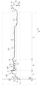
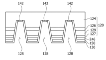
図1は本発明の一実施例に係る発光構造物の概念図であり、図2は本発明の一実施例に係る発光構造物のアルミニウム組成比を示したグラフである。 FIG. 1 is a conceptual diagram of a light emitting structure according to an embodiment of the present invention, and FIG. 2 is a graph showing the aluminum composition ratio of the light emitting structure according to an embodiment of the present invention.
図1を参照すると、実施例に係る半導体素子は第1導電型半導体層124、第2導電型半導体層127、および第1導電型半導体層124と第2導電型半導体層127の間に配置される活性層126を含む発光構造物120を含む。
Referring to FIG. 1, the semiconductor device according to the embodiment includes a first conductive
第1導電型半導体層124はIII-V族、II-VI族などの化合物半導体で具現され得、第1ドーパントがドーピングされ得る。第1導電型半導体層124はInx1Aly1Ga1-x1-y1N(0≦x1≦1、0≦y1≦1、0≦x1+y1≦1)の組成式を有する半導体材料、例えばGaN、AlGaN、InGaN、InAlGaNなどから選択され得る。そして、第1ドーパントはSi、Ge、Sn、Se、Teのようなn型ドーパントであり得る。第1ドーパントがn型ドーパントである場合、第1ドーパントがドーピングされた第1導電型半導体層124はn型半導体層であり得る。
The first conductive
活性層126は第1導電型半導体層124と第2導電型半導体層127の間に配置される。活性層126は第1導電型半導体層124を通じて注入される電子(または正孔)と第2導電型半導体層127を通じて注入される正孔(または電子)が会う層である。活性層126は電子と正孔が再結合することによって低いエネルギー準位に遷移し、紫外線波長を有する光を生成することができる。
The
活性層126は単一井戸構造、多重井戸構造、単一量子井戸構造、多重量子井戸(Multi Quantum Well;MQW)構造、量子ドット構造または量子細線構造のうちいずれか一つの構造を有することができ、活性層126の構造はこれに限定されない。
The
第2導電型半導体層127は活性層126上に形成され、III-V族、II-VI族などの化合物半導体で具現され得、第2導電型半導体層127に第2ドーパントがドーピングされ得る。第2導電型半導体層127はInx5Aly2Ga1-x5-y2N(0≦x5≦1、0≦y2≦1、0≦x5+y2≦1)の組成式を有する半導体物質またはAlInN、AlGaAs、GaP、GaAs、GaAsP、AlGaInPのうち選択された物質で形成され得る。第2ドーパントがMg、Zn、Ca、Sr、Baなどのようなp型ドーパントである場合、第2ドーパントがドーピングされた第2導電型半導体層127はp型半導体層であり得る。
The second conductive
第2導電型半導体層127は第2-1~第2-3導電型半導体層127a、127b、127cを含むことができる。第2-1導電型半導体層127aは第2-2導電型半導体層127bよりアルミニウム組成が小さくてもよい。
The second conductive
活性層126と第2導電型半導体層127の間には電子遮断層129が配置され得る。電子遮断層129は第1導電型半導体層124から供給された電子が第2導電型半導体層127に抜け出る流れを遮断して、活性層126内で電子と正孔が再結合する確率を高めることができる。電子遮断層129のエネルギーバンドギャップは活性層126および/または第2導電型半導体層127のエネルギーバンドギャップより大きくてもよい。
An
電子遮断層129はInx1Aly1Ga1-x1-y1N(0≦x1≦1、0≦y1≦1、0≦x1+y1≦1)の組成式を有する半導体材料、例えばAlGaN、InGaN、InAlGaNなどから選択され得るがこれに限定されない。電子遮断層129はアルミニウム組成が高い第1層129bとアルミニウム組成が低い第2層129aが交互に配置され得る。
The
図2を参照すると、第1導電型半導体層124、障壁層126b、井戸層126a、第2-1~第2-3導電型半導体層127a、127b、127cはいずれもアルミニウムを含むことができる。したがって、第1導電型半導体層124、障壁層126b、井戸層126a、第2-1~第2-3導電型半導体層127a、127b、127cはAlGaNであり得る。しかし、必ずしもこれに限定されない。
Referring to FIG. 2, the first conductive
電子遮断層129はアルミニウム組成が50%~90%であり得る。遮断層129はアルミニウム組成が相対的に高い複数個の第1遮断層129aとアルミニウム組成が低い複数個の第2遮断層129bが交互に配置され得る。遮断層129のアルミニウム組成が50%未満である場合、電子を遮断するためのエネルギー障壁の高さが不十分であり得、活性層126から放出する光を遮断層129で吸収することができ、アルミニウム組成が90%を超過する場合、半導体素子の電気的特性が悪化し得る。
The
電子遮断層129は第1-1区間129-1と第1-2区間129-2を含むことができる。第1-1区間129-1は遮断層129に近づくほどアルミニウム組成が高くなり得る。第1-1区間129-1のアルミニウム組成は80%~100%であり得る。すなわち、第1-1区間129-1はAlGaNでもよく、AlNでもよい。または第1-1区間129-1はAlGaNとAlNが交互に配置される超格子層でもよい。
The
第1-1区間129-1の厚さは約0.1nm~4nmであり得る。第1-1区間129-1の厚さが0.1nmより薄い場合、電子の移動を効率的に遮断できない問題点があり得る。また、第1-1区間129-1の厚さが4nmより厚い場合、活性層に正孔が注入される効率が低下する問題点があり得る。 The thickness of the 1-1 section 129-1 may be approximately 0.1 nm to 4 nm. If the thickness of the 1-1 section 129-1 is thinner than 0.1 nm, there may be a problem that the movement of electrons cannot be efficiently blocked. Furthermore, if the thickness of the 1-1 section 129-1 is thicker than 4 nm, there may be a problem that the efficiency with which holes are injected into the active layer decreases.
第1-2区間129-2はアンドープ(undoped)された区間を含むことができる。第1-2区間129-2はドーパントが第2導電型半導体層127から活性層126に拡散することを防止する役割を遂行することができる。
The 1-2nd section 129-2 may include an undoped section. The 1-2 section 129-2 may serve to prevent dopants from diffusing from the second conductive
第2-2導電型半導体層127bの厚さは10nmより大きく200nmより小さくてもよい。例示的に第2-2導電型半導体層127bの厚さは25nmであり得る。第2-2導電型半導体層127bの厚さが10nmより小さい場合、水平方向に抵抗が増加して電流注入効率が低下し得る。また、第2-2導電型半導体層127bの厚さが200nmより大きい場合、垂直方向に抵抗が増加して電流注入効率が低下し得る。
The thickness of the 2-2nd conductivity
第2-2導電型半導体層127bのアルミニウム組成は井戸層126aのアルミニウム組成より高くてもよい。紫外線光を生成するために井戸層126aのアルミニウム組成は約30%~70%であり得る。もし、第2-2導電型半導体層127bのアルミニウム組成が井戸層126aのアルミニウム組成より低い場合、第2-2導電型半導体層127bが光を吸収するため、光抽出効率が低下し得る。しかし、発光構造物の結晶性の低下を防止するためには、必ずしもこれに限定されない。例示的に第2-2導電型半導体層127bの一部の区間でのアルミニウム組成は井戸層126aのアルミニウム組成より低くてもよい。
The aluminum composition of the 2-2nd conductivity
第2-2導電型半導体層127bのアルミニウム組成は40%より大きく80%より小さくてもよい。第2-2導電型半導体層127bのアルミニウム組成は40%より小さい場合、光を吸収する問題があり、80%より大きい場合には電流注入効率が悪化する問題がある。例示的に、井戸層126aのアルミニウム組成が30%である場合、第2-2導電型半導体層127bのアルミニウム組成は40%であり得る。
The aluminum composition of the 2-2nd conductivity
第2-1導電型半導体層127aのアルミニウム組成は井戸層126aのアルミニウム組成より低くてもよい。第2-1導電型半導体層127aのアルミニウム組成が井戸層126aのアルミニウム組成より高い場合、p-オーミック電極の間の抵抗が高くなって十分なオーミックが行われず、電流注入効率が低下する問題がある。
The aluminum composition of the 2-1 conductivity
第2-1導電型半導体層127aのアルミニウム組成は1%より大きく50%より小さくてもよい。50%より大きい場合、pオーミック電極と十分なオーミックが行われ得ず、組成が1%より小さい場合、ほぼGaN組成と近くなって光を吸収する問題がある。
The aluminum composition of the 2-1 conductivity
第2-1導電型半導体層127aの厚さは1nm~30nm、または1nm~10nmであり得る。前述した通り、第2-1導電型半導体層127aはオーミックのためにアルミニウムの組成が低いので、紫外線光を吸収することができる。したがって、できるだけ第2-1導電型半導体層127aの厚さを薄く制御することが光出力の観点で有利であり得る。
The thickness of the 2-1st conductivity
しかし、第2-1導電型半導体層127aの厚さが1nm以下に制御される場合、一部の区間は第2-1導電型半導体層127aが配置されず、第2-2導電型半導体層127bが発光構造物120の外部に露出する領域が発生し得る。また、厚さが30nmより大きい場合、第2-1導電型半導体層127aが吸収する光量が過度に大きくなって光出力効率が減少し得る。
However, when the thickness of the 2-1st conductivity
第2-1導電型半導体層127aの厚さは第2-2導電型半導体層127bの厚さより小さくてもよい。第2-2導電型半導体層127bと第2-1導電型半導体層127aの厚さ比は1.5:1~20:1であり得る。厚さ比が1.5:1より小さい場合、第2-2導電型半導体層127bの厚さが過度に薄くなるため、電流注入効率が減少し得る。また、厚さ比が20:1より大きい場合、第2-1導電型半導体層127aの厚さが過度に薄くなるため、オーミックの信頼性が低下し得る。
The thickness of the 2-1st conductivity
第2-2導電型半導体層127bのアルミニウム組成は活性層126から遠くなるほど小さくなり得る。また、第2-1導電型半導体層127aのアルミニウム組成は活性層126から遠くなるほど小さくなり得る。
The aluminum composition of the 2-2nd conductivity
この時、第2-1導電型半導体層127aのアルミニウム減少幅は、第2-2導電型半導体層127bのアルミニウム減少幅より大きくてもよい。すなわち、第2-1導電型半導体層127aのAl組成比の厚さ方向に対する変化率は、第2-2導電型半導体層127bのAl組成比の厚さ方向に対する変化率より大きくてもよい。
At this time, the aluminum reduction width of the 2-1st conductivity
第2-2導電型半導体層127bの厚さは第2-1導電型半導体層127aより厚い反面、アルミニウム組成は井戸層126aより高くなければならないため、減少幅が相対的に緩やかであり得る。しかし、第2-1導電型半導体層127aは厚さが薄く、アルミニウム組成の変化幅が大きいため、アルミニウム組成の減少幅が相対的に大きくてもよい。
Although the thickness of the 2-2nd conductivity
第2-3導電型半導体層127cは均一なアルミニウム組成を有することができる。第2-3導電型半導体層127cの厚さは20nm~60nmであり得る。第2-3導電型半導体層127cのアルミニウム組成は40%~70%であり得る。
図3は本発明の第1実施例に係る発光構造物のSIMSグラフであり、図4は図3の一部拡大図である。
The second-third conductivity
FIG. 3 is a SIMS graph of the light emitting structure according to the first embodiment of the present invention, and FIG. 4 is a partially enlarged view of FIG. 3.
図3および図4を参照すると、発光構造物は厚さが減少する方向にアルミニウム組成とP型不純物(Mg)の組成が変化し得る。第2導電型半導体層127から第2導電型半導体層127の表面方向へ向かうほどアルミニウムの組成は低くなり、P型不純物(Mg)の組成は高くなり得る。
Referring to FIGS. 3 and 4, the light emitting structure may have a change in aluminum composition and a P-type impurity (Mg) composition as the thickness decreases. The composition of aluminum may become lower and the composition of P-type impurity (Mg) may become higher as it goes from the second conductivity
第2導電型半導体層127は表面(厚さが0の地点、第1面)から第2地点P21までの第2最短距離W2と表面から第1地点P11までの第1最短距離W1の比W2:W1が1:1.25~1:100、または1:1.25~1:10であり得る。
The second conductive
第2最短距離W2と第1最短距離W1の比W2:W1が1:1.25より小さい場合には、第1最短距離W1と第2最短距離W2が近くなってアルミニウム組成の変化が急激となる問題が発生し得る。また、比W2:W1が1:100より大きい場合、第2導電型半導体層127の厚さが過度に厚くなって第2導電型半導体層127の結晶性が低下したり、基板方向に印加される応力が強くなり得るため、活性層から放出する光の波長が変化する問題がある。
When the ratio W2:W1 of the second shortest distance W2 and the first shortest distance W1 is smaller than 1:1.25, the first shortest distance W1 and the second shortest distance W2 become close, and the aluminum composition changes rapidly. Problems may occur. In addition, when the ratio W2:W1 is larger than 1:100, the thickness of the second conductive
ここで、第1地点P11は活性層のうち第2導電型半導体層127と最も近い井戸層126aのアルミニウム組成と同じ組成を有する地点であり得る。第1地点P11の範囲はSIMSで測定したスペクトルで定義することができる。第1地点P11の範囲は活性層の井戸層でのアルミニウム含量と同じ第2導電型半導体層で定義することができる。
Here, the first point P11 may be a point having the same aluminum composition as the
第1地点P11を測定して定義するためにSIMSスペクトルによる方法を適用することができるが、必ずしもこれに限定されはしない。他の例としてTEM、XRD測定方法を適用することができるが、簡便にはSIMSスペクトルを通じて定義することができる。 A SIMS spectrum method can be applied to measure and define the first point P11, but is not necessarily limited thereto. As other examples, TEM and XRD measurement methods can be applied, but it can be simply defined through SIMS spectra.
第2地点P21はSIMSスペクトルで第2導電型半導体層のドーパント(例えば、Mg)に対するスペクトルとアルミニウムに対するスペクトルが交差する地点であり得る。 The second point P21 may be a point where a spectrum for a dopant (eg, Mg) of the second conductive type semiconductor layer and a spectrum for aluminum intersect in the SIMS spectrum.
測定において、第2導電型半導体層のドーパントに対する値の単位は異なり得るが、第2導電型半導体層のアルミニウム組成に対する変曲点を含む領域と第2導電型半導体層のドーパントに対するスペクトルが交差する地点を含む範囲内で、第2-1導電型半導体層127aと第2-2導電型半導体層127bの境界領域が含まれ得る。したがって、導電型第2-1半導体層127aと第2-2導電型半導体層127bの境界領域を測定することができ、その範囲を定義することができる。
In the measurement, the unit of the value for the dopant of the second conductivity type semiconductor layer may be different, but the region including the inflection point for the aluminum composition of the second conductivity type semiconductor layer and the spectrum for the dopant of the second conductivity type semiconductor layer intersect. A boundary region between the 2-1st conductivity
しかし、必ずしもこれに限定されず、第2地点P21はアルミニウム組成が5%~55%の領域内に位置した地点であり得る。第2地点P21のアルミニウム組成が5%未満である場合、第2-1導電型半導体層127aの厚さが過度に薄くなり得るため、半導体素子の消費電力の効率が低下し得、55%を超過する場合、第2-1導電型半導体層127aの厚さが過度に厚くなるため、光抽出効率が低下する問題が発生し得る。この時、第2地点P21のアルミニウム組成は第1地点P11のアルミニウム組成より小さくてもよい。例示的に第2地点P21はアルミニウム組成が40%~70%であり得る。
However, the present invention is not limited thereto, and the second point P21 may be a point located in a range where the aluminum composition is 5% to 55%. If the aluminum composition at the second point P21 is less than 5%, the thickness of the 2-1 conductivity
例示的に第1最短距離W1は25nm~100nmであり得、第2最短距離W2は1nm~20nmであり得る。 For example, the first shortest distance W1 may be 25 nm to 100 nm, and the second shortest distance W2 may be 1 nm to 20 nm.
電子遮断層129の平均アルミニウム組成と第1地点P11でのアルミニウム組成の第1差H1と電子遮断層の平均アルミニウム組成と第2地点P21でのアルミニウム組成の第2差H2の比H1:H2は1:1.2~1:10であり得る。
The ratio H1:H2 of the first difference H1 between the average aluminum composition of the
第1差と第2差の比H1:H2が1:1.2より小さい場合、第1地点P11と第2点の間の区間のアルミニウム組成の変化が緩やかであるため、コンタクト層でアルミニウム組成を十分に低くし難い問題がある。また、第1差と第2差の比H1:H2が1:10より大きい場合、アルミニウム組成の変化が急激であるため、活性層から出射した光を吸収する確率が高くなり得る。 If the ratio H1:H2 of the first difference to the second difference is smaller than 1:1.2, the change in aluminum composition in the section between the first point P11 and the second point is gradual, so the aluminum composition in the contact layer The problem is that it is difficult to lower the value sufficiently. Furthermore, when the ratio H1:H2 of the first difference to the second difference is greater than 1:10, the aluminum composition changes rapidly, and the probability of absorbing light emitted from the active layer may increase.
図5は本発明の第2実施例に係る発光構造物のSIMSグラフであり、図6は図5の一部拡大図であり、図7は本発明の第3実施例に係る発光構造物のSIMSグラフであり、図8は図7の一部拡大図である。 FIG. 5 is a SIMS graph of a light emitting structure according to a second embodiment of the present invention, FIG. 6 is a partially enlarged view of FIG. 5, and FIG. 7 is a SIMS graph of a light emitting structure according to a third embodiment of the present invention. This is a SIMS graph, and FIG. 8 is a partially enlarged view of FIG. 7.
図5~図8を参照しても前述した第2最短距離W2と第1最短距離W1の比W2:W1が1:1.25~1:100、または1:1.25~1:10を満足することが分かる。例示的に図8を参照すると、第1地点P13と第2地点P23は非常に近接するように配置されることが分かる。 Referring to FIGS. 5 to 8, the ratio W2:W1 between the second shortest distance W2 and the first shortest distance W1 is 1:1.25 to 1:100, or 1:1.25 to 1:10. I know you will be satisfied. For example, referring to FIG. 8, it can be seen that the first point P13 and the second point P23 are arranged very close to each other.
また、電子遮断層129の平均アルミニウム組成と第1地点P12、P13でのアルミニウム組成の第1差と、電子遮断層の平均アルミニウム組成と第2地点P22、P23でのアルミニウム組成の第2差の比H1:H2は1:1.2~1:10を満足することが分かる。
Also, a first difference between the average aluminum composition of the
このような条件を満足する場合、第2導電型半導体層127の表面でアルミニウムの組成を1%~10%に調節することができる。
When these conditions are satisfied, the aluminum composition on the surface of the second conductive
図9は本発明の一実施例に係る半導体構造物の概念図であり、図10は本発明の一実施例に係る半導体構造物のアルミニウム組成比を示したグラフである。 FIG. 9 is a conceptual diagram of a semiconductor structure according to an embodiment of the present invention, and FIG. 10 is a graph showing the aluminum composition ratio of the semiconductor structure according to an embodiment of the present invention.
図9および図10を参照すると、実施例に係る半導体素子は第1導電型半導体層124、第2導電型半導体層127、および第1導電型半導体層124と第2導電型半導体層127の間に配置される活性層126を含む半導体構造物120を含む。
9 and 10, the semiconductor device according to the example includes a first conductive
本発明の実施例に係る半導体構造物120は紫外線波長帯の光を出力することができる。例示的に半導体構造物120は近紫外線波長帯の光UV-Aを出力してもよく、遠紫外線波長帯の光UV-Bを出力してもよく、深紫外線波長帯の光UV-Cを出力してもよい。波長範囲は半導体構造物120のAlの組成比によって決定され得る。
The
例示的に、近紫外線波長帯の光UV-Aは320nm~420nm範囲の波長を有することができ、遠紫外線波長帯の光UV-Bは280nm~320nm範囲の波長を有することができ、深紫外線波長帯の光UV-Cは100nm~280nm範囲の波長を有することができる。 Illustratively, the light UV-A in the near ultraviolet wavelength range may have a wavelength in the range of 320 nm to 420 nm, the light UV-B in the deep ultraviolet wavelength range may have a wavelength in the range of 280 nm to 320 nm, and the deep ultraviolet light The wavelength range of light UV-C can have a wavelength in the range of 100 nm to 280 nm.
半導体構造物120が紫外線波長帯の光を発光する時、半導体構造物120の各半導体層はアルミニウムを含むInx1Aly1Ga1-x1-y1N(0≦x1≦1、0<y1≦1、0≦x1+y1≦1)物質を含むことができる。ここで、Alの組成はIn原子量とGa原子量およびAl原子量を含む全体の原子量とAl原子量の割合で示すことができる。例えば、Al組成が40%である場合、Gaの組成は60%であるAl40Ga60Nであり得る。
When the
また、実施例の説明において組成が低いまたは高いという意味は、各半導体層の組成%の差(および/または%ポイント)と理解され得る。例えば、第1半導体層のアルミニウム組成が30%であって、第2導電型半導体層のアルミニウム組成が60%である場合、第2導電型半導体層のアルミニウム組成は第1半導体層のアルミニウム組成より30%より高いと表現することができる。 Furthermore, in the description of the examples, the meaning of low or high composition can be understood as the difference in composition percentage (and/or percentage point) of each semiconductor layer. For example, if the aluminum composition of the first semiconductor layer is 30% and the aluminum composition of the second conductivity type semiconductor layer is 60%, the aluminum composition of the second conductivity type semiconductor layer is lower than the aluminum composition of the first semiconductor layer. It can be expressed as higher than 30%.
第1導電型半導体層124はIII-V族、II-VI族などの化合物半導体で具現され得、第1ドーパントがドーピングされ得る。第1導電型半導体層124はInx1Aly1Ga1-x1-y1N(0≦x1≦1、0<y1≦1、0≦x1+y1≦1)の組成式を有する半導体材料、例えばAlGaN、AlN、InAlGaNなどから選択され得る。そして、第1ドーパントはSi、Ge、Sn、Se、Teのようなn型ドーパントであり得る。第1ドーパントがn型ドーパントである場合、第1ドーパントがドーピングされた第1導電型半導体層124はn型半導体層であり得る。ただし、これに限定されず、第1導電型半導体層124はp型半導体層であり得る。
The first conductive
第1導電型半導体層124は第1-1導電型半導体層124a、第1-2導電型半導体層124c、および第1-1導電型半導体層124aと第1-2導電型半導体層124cの間に配置された中間層124bを含むことができる。
The first conductive
第1-1導電型半導体層124aのアルミニウム組成は50%~80%であり得る。第1-1導電型半導体層124aのアルミニウム組成が50%以上であるとき、活性層126から放出される深紫外線波長帯の光UV-Cの吸収率を低くして光抽出効率を改善させることができ、80%以下であるとき、活性層126での電流注入特性および第1-1導電型半導体層124a内での電流拡散特性を確保することができる。
The aluminum composition of the 1-1 conductivity
第1-2導電型半導体層124cは第1-1導電型半導体層124aより活性層126に近く配置され得る。第1-2導電型半導体層124cのアルミニウム組成は第1-1導電型半導体層124aより低くてもよい。
The 1-2nd conductivity
半導体構造物120が深紫外線波長帯の光UV-Cを放出する場合、第1-2導電型半導体層124cのアルミニウム組成は40%~70%であり得る。
When the
第1-2導電型半導体層124cのアルミニウム組成が40%以上であるとき、活性層126から放出される深紫外線波長帯の光UV-Cの吸収率を低くして光抽出効率を改善させることができ、70%以下であるとき、活性層126での電流注入特性および第1-2導電型半導体層124c内での電流拡散特性を確保することができる。
When the aluminum composition of the first-second conductivity
第1-1導電型半導体層124aと第1-2導電型半導体層124cのアルミニウム組成は、井戸層126aのアルミニウム組成より高くてもよい。したがって、活性層126が紫外線領域の波長を有する光を放出する場合、紫外線領域の波長を有する光に対する半導体構造物120内で吸収率を低くすることができる。
The aluminum composition of the 1-1st conductivity
また、第1-2導電型半導体層124cのアルミニウム組成より第1-1導電型半導体層124aのアルミニウム組成が高い場合、屈折率の差によって、活性層126から半導体構造物120の外部に光が抽出されるのにさらに有利であり得る。したがって、半導体構造物120の光抽出効率が改善され得る。
Further, when the aluminum composition of the first-first conductivity
第1-2導電型半導体層124cの厚さは、第1-1導電型半導体層124aの厚さより薄くてもよい。第1-1導電型半導体層124aは第1-2導電型半導体層124cの厚さの130%以上であり得る。このような構成によると、アルミニウム組成が高い第1-1導電型半導体層124aの厚さを十分に確保した後に中間層124bが配置されるため、全体の半導体構造物120の結晶性が向上し得る。
The thickness of the 1-2nd conductivity
中間層124bのアルミニウム組成は、第1導電型半導体層124および第2導電型半導体層124のアルミニウム組成より低くてもよい。中間層124bは、成長基板を除去するLLO(Laser Lift-off)工程時に半導体構造物120に照射されるレーザーを吸収して活性層126が損傷することを防止する役割を遂行することができる。したがって、実施例に係る半導体素子は、LLO(Laser Lift-off)工程時に活性層126の損傷を防止することができるため、光出力および電気的特性が向上し得る。
The aluminum composition of the
また、中間層124bが第1電極と接する場合、中間層124bと第1電極の間の抵抗を低くして電流注入効率を確保するために、中間層124bのアルミニウム組成は第1-1導電型半導体層124a、第1-2導電型半導体層124cのアルミニウム組成より低くてもよい。
Further, when the
中間層124bの厚さとアルミニウム組成は、LLO工程時に半導体構造物120に照射されるレーザーを吸収するために適切に調節され得る。したがって、中間層124bのアルミニウム組成は、LLO工程時に使うレーザー光の波長に対応され得る。
The thickness and aluminum composition of the
LLO用レーザーが200nm~300nmである場合、中間層124bのアルミニウム組成は30%~70%であり、厚さは1nm~10nmであり得る。
When the LLO laser is 200 nm to 300 nm, the aluminum composition of the
例示的にLLO用レーザーの波長が270nmより低くなる場合、LLO用レーザー波長に対応するように中間層124bのアルミニウムの組成が高くなり得る。例示的に中間層124bのアルミニウム組成は50%~70%に高くなり得る。
For example, when the wavelength of the LLO laser is lower than 270 nm, the aluminum composition of the
中間層124bのアルミニウム組成が井戸層126aのアルミニウム組成より高くなると、中間層124bは活性層126から出射した光を吸収しないことがある。したがって、光抽出効率が向上し得る。実施例によると、LLO用レーザーは井戸層126aの発光波長より低い波長が選択され得る。したがって、中間層124bは、LLO用レーザーは吸収しつつ、井戸層126aから出射する光は吸収しないように、適切なアルミニウム組成を有することができる。
If the aluminum composition of the
中間層124bは第1導電型半導体層124よりアルミニウム組成が低い第1中間層(図示されず)、および第1導電型半導体層124よりアルミニウム組成が高い第2中間層(図示されず)を含むこともできる。第1中間層と第2中間層は交互に複数個が配置されてもよい。
The
活性層126は第1導電型半導体層124と第2導電型半導体層127の間に配置され得る。活性層126は複数の井戸層126aと複数の障壁層126bを含むことができる。井戸層126aは第1導電型半導体層124を通じて注入される第1キャリア(電子または正孔)と第2導電型半導体層127を通じて注入される第2キャリア(正孔または電子)が会う層である。伝導帯の第1キャリア(または第2キャリア)と価電子帯の第2キャリア(または第1キャリア)が活性層126の井戸層126aで再結合すると、井戸層126aの伝導帯と井戸層126aの価電子帯のエネルギーレベルの差(エネルギーバンドギャップ)に対応する波長を有する光が発生し得る。
The
活性層126は単一井戸構造、多重井戸構造、単一量子井戸構造、多重量子井戸(Multi Quantum Well;MQW)構造、量子ドット構造または量子細線構造のうちいずれか一つの構造を有することができ、活性層126の構造はこれに限定されない。
The
活性層126は複数個の井戸層126aと障壁層126bを含むことができる。井戸層126aと障壁層126bは、Inx2Aly2Ga1-x2-y2N(0≦x2≦1、0<y2≦1、0≦x2+y2≦1)の組成式を有することができる。井戸層126aは発光する波長によりアルミニウム組成が変わり得る。
The
第2導電型半導体層127は活性層126上に形成され、III-V族、II-VI族などの化合物半導体で具現され得、第2導電型半導体層127に第2ドーパントがドーピングされ得る。
The second conductive
第2導電型半導体層127は、Inx5Aly2Ga1-x5-y2N(0≦x5≦1、0<y2≦1、0≦x5+y2≦1)の組成式を有する半導体物質またはAlInN、AlGaAs、GaP、GaAs、GaAsP、AlGaInPのうち選択された物質で形成され得る。
The second conductive
第2ドーパントがMg、Zn、Ca、Sr、Baなどのようなp型ドーパントである場合、第2ドーパントがドーピングされた第2導電型半導体層127はp型半導体層であり得る。ただし、これに限定されず、第2導電型半導体層124はn型半導体層でもよい。
When the second dopant is a p-type dopant such as Mg, Zn, Ca, Sr, Ba, etc., the second conductive
第2導電型半導体層127は第2-1~第2-3導電型半導体層127a、127b、127cを含むことができる。第2-1導電型半導体層127aは第2-2導電型半導体層127bおよび第2-3導電型半導体層127cよりアルミニウム組成が小さくてもよい。
The second conductive
遮断層129は活性層126と第2導電型半導体層127の間に配置され得る。遮断層129は第1導電型半導体層124から供給された第1キャリアが第2導電型半導体層127に抜け出る流れを遮断して、活性層126内で電子と正孔が再結合する確率を高めることができる。遮断層129のエネルギーバンドギャップは、活性層126および/または第2導電型半導体層127のエネルギーバンドギャップより大きくてもよい。遮断層129は第2ドーパントがドーピングされるため、第2導電型半導体層127の一部の領域と定義されてもよい。
The
遮断層129は、Inx1Aly1Ga1-x1-y1N(0≦x1≦1、0<y1≦1、0≦x1+y1≦1)の組成式を有する半導体材料、例えばAlGaN、AlN、InAlGaNなどから選択され得るがこれに限定されない。
The
実施例によると、第1導電型半導体層124、活性層126、第2導電型半導体層127、および遮断層129はいずれもアルミニウムを含むことができる。したがって、第1導電型半導体層124、活性層126、第2導電型半導体層127、および遮断層129はAlGaN、InAlGaNまたはAlN組成を有することができる。
According to example embodiments, the first conductive
遮断層129は、アルミニウム組成が井戸層126aのアルミニウム組成より高くてもよい。例示的に遮断層129はアルミニウム組成は50%~100%であり得る。遮断層129のアルミニウム組成が50%以上である場合、第1キャリアを遮断するための十分なエネルギー障壁を有することができ、活性層126から放出する光を吸収しないことがある。
The aluminum composition of the
遮断層129は第1-1区間129aと第1-2区間129cを含むことができる。
The
第1-1区間129aは第1導電型半導体層124から第2導電型半導体層127に向かう方向へ向かうほどアルミニウム組成が高くなり得る。
In the 1-1
第1-1区間129aのアルミニウム組成は80%~100%であり得る。したがって、遮断層129の第1-1区間129aは半導体構造物120内でAl組成が最も高い部分であり得る。
The aluminum composition of the 1-1
第1-1区間129aはAlGaNまたはAlNを含むことができる。または第1-1区間129aはAlGaNとAlNが交互に配置される超格子層でもよい。
The 1-1
第1-1区間129aの厚さは約0.1nm~4nmであり得る。第1キャリアの第2導電型半導体層127での移動を効率的に遮断するためには、第1-1区間129aの厚さは0.1nm以上で配置することができる。また、第2導電型半導体層127から活性層126に第2キャリアを注入する注入効率を確保するために、第1-1区間129aの厚さは4nm以下で配置することができる。
The thickness of the 1-1
実施例の第1-1区間129aは、正孔の注入効率と電子(Electron)の遮断効率を確保するために、第1-1区間129-aの厚さを0.1nm以上~4nm以下で配置したが必ずしもこれに限定されない。例示的に第1キャリアの遮断機能と第2キャリアの注入機能のうちいずれか一つを選択的により大きく確保しなければならない必要がある場合、前記言及した数値範囲から外れてもよい。 In the 1-1 section 129-a of the embodiment, the thickness of the 1-1 section 129-a is 0.1 nm or more and 4 nm or less in order to ensure hole injection efficiency and electron blocking efficiency. However, the arrangement is not necessarily limited to this. For example, if one of the blocking function of the first carrier and the injection function of the second carrier needs to be selectively increased, the numerical value may be outside the above-mentioned numerical range.
第1-1区間129aと第1-2区間129cの間に配置された第1-3区間129bは、ドーパントを含まないアンドープ(undoped)された区間を含むことができる。したがって、第1-3区間129bは第2ドーパントが第2導電型半導体層127から活性層126に拡散することを防止する役割を遂行することができる。
The 1-3
第2導電型半導体層127は第2-1~第2-3導電型半導体層127a、127b、127cを含むことができる。
The second conductive
第2-2導電型半導体層127bの厚さは10nmより大きく50nmより小さくてもよい。例示的に第2-2導電型半導体層127bの厚さは25nmであり得る。第2-2導電型半導体層127bの厚さが10nm以上の場合、第2-2導電型半導体層127bの電流拡散特性を確保することができる。また、厚さが50nm以下である場合、活性層126に注入する第2キャリアの注入効率を確保することができ、活性層126から放出される光の第2-2導電型半導体層127bでの吸収率を低くすることができる。
The thickness of the 2-2nd conductivity
第2-2導電型半導体層127bのアルミニウム組成は、井戸層126aのアルミニウム組成より高くてもよい。紫外線光を生成するために、井戸層126aのアルミニウム組成は約30%~70%であり得る。したがって、第2-2導電型半導体層127bのアルミニウム組成は40%以上80%以下であり得る。
The aluminum composition of the 2-2nd conductivity
第2-2導電型半導体層127bのアルミニウム組成が40%以上である場合、光を吸収する問題を改善させることができ、80%以下である場合には電流注入効率が悪化する問題を改善させることができる。例示的に、井戸層126aのアルミニウム組成が30%である場合、第2-2導電型半導体層127bのアルミニウム組成は40%であり得る。
When the aluminum composition of the 2-2 conductive
第2-1導電型半導体層127aのアルミニウム組成は、井戸層126aのアルミニウム組成より低くてもよい。第2-1導電型半導体層127aのアルミニウム組成が井戸層126aのアルミニウム組成より高い場合、第2電極の間の抵抗が高くなって十分なオーミックが行われず、電流注入効率が低下する問題がある。
The aluminum composition of the 2-1st conductivity
第2-1導電型半導体層127aのアルミニウム組成は1%以上50%以下であり得る。50%以下である場合、第2電極との抵抗が低くなり得、組成が1%以上である場合、第2-1導電型半導体層127a内で光を吸収する問題を改善させることができる。第2-1導電型半導体層127aのアルミニウム組成は中間層124bのアルミニウム組成より小さくてもよい。
The aluminum composition of the 2-1st conductivity
第2-1導電型半導体層127aの厚さは1nm~30nmであり得る。第2-1導電型半導体層127aは紫外線光を吸収することができるため、できるだけ第2-1導電型半導体層127aの厚さを薄く制御することが光出力の観点で有利であり得る。
The thickness of the 2-1st conductivity
しかし、第2-1導電型半導体層127aの厚さが1nm以上である場合、第2-1導電型半導体層127aの抵抗を減少させることができるため、半導体素子の電気的特性が改善され得る。また、厚さが30nm以下である場合、第2-1導電型半導体層127aが吸収する光量を減らして光出力効率を改善させることができる。
However, when the thickness of the 2-1st conductivity
第2-1導電型半導体層127aの厚さは、第2-2導電型半導体層127bの厚さより小さくてもよい。第2-1導電型半導体層127aと第2-2導電型半導体層127bの厚さ比は1:1.5~1:20であり得る。厚さ比が1:1.5より大きい場合、第2-2導電型半導体層127bの厚さが増加するため、電流注入効率が改善され得る。また、厚さ比が1:20より小さい場合、第2-1導電型半導体層127aの厚さが増加するため、結晶性が低下する問題を改善させることができる。もし、第2-1導電型半導体層127aの厚さが過度に薄くなると、その厚さ範囲内でアルミニウム組成を急激に変化させなければならないため、結晶性が低下し得る。
The thickness of the 2-1st conductivity
第2-2導電型半導体層127bのアルミニウム組成は、活性層126から遠くなるほど小さくなり得る。また、第2-1導電型半導体層127aのアルミニウム組成は、活性層126から遠くなるほど小さくなり得る。
The aluminum composition of the 2-2nd conductivity
この時、第2-1導電型半導体層127aの厚さに対するアルミニウム減少幅は、第2-2導電型半導体層127bの厚さに対するアルミニウム減少幅より大きくてもよい。すなわち、第2-1導電型半導体層127aのAl組成比の厚さ方向に対する変化率は、第2-2導電型半導体層127bのAl組成比の厚さ方向に対する変化率より大きくてもよい。
At this time, the aluminum reduction width with respect to the thickness of the 2-1st conductive
第2-1導電型半導体層127aは、第2電極との低い接触抵抗のために井戸層126aよりアルミニウム組成が低くなり得る。したがって、第2-1導電型半導体層127aは井戸層126aから発光する光を一部吸収することができる。
The 2-1st conductivity
したがって、第2-1導電型半導体層127aは光が吸収されることを抑制するために、第2-1導電型半導体層127aの厚さを1nm以上~30nm以下で配置することができる。
Therefore, in order to suppress absorption of light, the 2-1 conductive
その結果、第2-1導電型半導体層127aは、厚さは薄くなる反面、アルミニウムの変化幅は相対的に大きいため、厚さに対するアルミニウム減少幅が相対的に大きくてもよい。
As a result, although the thickness of the 2-1st conductivity
これに反し、第2-2導電型半導体層127bは、厚さは第2-1導電型半導体層127aより厚い反面、アルミニウム組成は井戸層126aより高いか同じであるため、減少幅が相対的に緩やかであり得る。
On the other hand, although the thickness of the 2-2nd conductivity
第2-1導電型半導体層127aは、厚さが薄く厚さに対するアルミニウム組成の変化幅が大きいため、相対的にゆっくり成長させながらアルミニウムの組成を変化させることができる。
The 2-1st conductivity
第2-3導電型半導体層127cは均一なアルミニウム組成を有することができる。第2-3導電型半導体層127cの厚さは20nm~60nmであり得る。第2-3導電型半導体層127cのアルミニウム組成は40%~70%であり得る。第2-3導電型半導体層127cのアルミニウム組成が40%以上であるとき、第2-1導電型半導体層127a、第2-2導電型半導体層127bの結晶性が低下しないことができ、70%未満であるとき、前記第2-1導電型半導体層127a、第2-2導電型半導体層127bのアルミニウム組成が急激に変化して発生する結晶性が低下する問題を防止することができるため、半導体素子の電気的特性を向上させることができる。
The second-third conductivity
前述した通り、第2-1導電型半導体層127aの厚さは1nm~10nmであり、第2-2導電型半導体層127bの厚さは10nm~50nmであり、第2-3導電型半導体層127cの厚さは20nm~60nmであり得る。
As described above, the thickness of the 2-1 conductivity
したがって、第2-1導電型半導体層127aの厚さと第2導電型半導体層127の全体厚さの比は、1:3~1:120であり得る。1:3より大きい場合、第2-1導電型半導体層127aが半導体素子の電気的特性(例えば動作電圧)を確保することができ、1:120より小さい場合、半導体素子の光学的特性(例えば光出力)を確保することができる。しかし、必ずしもこれに限定されるものではなく、第2-1導電型半導体層127aの厚さと第2導電型半導体層127の全体厚さの比は、1:3~1:50または1:3~1:70であり得る。
Therefore, the ratio of the thickness of the 2-1st conductive
本発明の実施例に係る第2導電型半導体層127は、半導体構造物内でアルミニウム組成が最も高い第1地点P1、およびアルミニウム組成が最も低い第3地点P3を含むことができる。ここで第1地点P1はアルミニウム組成が最も高い遮断層129の第1-1区間129aであり得、第3地点P3はアルミニウムが最も低い第2-1導電型半導体層127aであり得る。
The second
第1導電型半導体層124は、第1導電型半導体層内でアルミニウム組成が最も高い第2地点P2、およびアルミニウム組成が最も低い第4地点P4を含むことができる。第2地点P2は第1-1導電型半導体層124aおよび/または第1-2導電型半導体層124cであり得、第4地点P4は中間層124bであり得る。
The first conductive
第1-1区間129aのアルミニウム組成は80%~100%であり得る。第2-1導電型半導体層127aのアルミニウム組成は1%以上50%であり得る。この時、第2-1導電型半導体層127aのアルミニウム組成は井戸層126aのアルミニウム組成より小さくてもよい。
The aluminum composition of the 1-1
したがって、第3地点P3と第1地点P1の間のアルミニウム組成の比は、1:4~1:100であり得る。アルミニウム組成の比が1:4以上である場合、第1地点P1のアルミニウム組成が増加して第1キャリアが第2導電型半導体層を通り過ぎることを効果的に遮断することができる。また、アルミニウム組成の比が1:100以下である場合、第3地点P3のアルミニウムが増加して第3地点P3が光を吸収する問題を改善させることができる。 Therefore, the aluminum composition ratio between the third point P3 and the first point P1 may be 1:4 to 1:100. When the aluminum composition ratio is 1:4 or more, the aluminum composition at the first point P1 increases and it is possible to effectively block the first carriers from passing through the second conductive type semiconductor layer. Furthermore, when the aluminum composition ratio is 1:100 or less, the amount of aluminum at the third point P3 increases, and the problem of the third point P3 absorbing light can be improved.
第1-1導電型半導体層124aのアルミニウム組成は、50%~80%であり得る。中間層124bのアルミニウム組成は、30%~70%であり得る。この時、中間層124bのアルミニウム組成は第1-1導電型半導体層より小さくてもよい。したがって、第4地点P4と第2地点P2の間のアルミニウム組成の比は、1:0.5~1:0.9であり得る。
The aluminum composition of the 1-1st conductivity
アルミニウム組成比が1:0.5以上である場合、第1-1導電型半導体層124aのアルミニウム組成が大きくなって結晶性が向上し得る。また、アルミニウム組成比が1:0.9以下である場合、中間層124bのアルミニウム組成が大きくなるので、紫外線波長帯の光を吸収する問題を改善させることができる。
When the aluminum composition ratio is 1:0.5 or more, the aluminum composition of the 1-1st conductivity
図11aおよび図11bは本発明の一実施例に係る半導体構造物のSIMS(Secondary Ion Mass Spectrometry、以下SIMS)データであり、図11cおよび図11dは本発明の他の実施例に係る半導体構造物のSIMSデータであり、図12は図11a~図11dのアルミニウム相対イオン強度を示す図面であり、図13aは図12の(a)のSIMSデータを一部拡大した図面であり、図13bは図12の(b)のSIMSデータをリニアスケールに変換した図面である。 11a and 11b are SIMS (Secondary Ion Mass Spectrometry, hereinafter SIMS) data of a semiconductor structure according to one embodiment of the present invention, and FIGS. 11c and 11d are data of a semiconductor structure according to another embodiment of the present invention. FIG. 12 is a drawing showing the aluminum relative ion intensity in FIGS. 11a to 11d, FIG. 13a is a partially enlarged view of the SIMS data in FIG. It is a drawing obtained by converting the SIMS data of No. 12 (b) into a linear scale.
図11aを参照すると、半導体構造物は第1導電型半導体層124から第2導電型半導体層127に行くほどアルミニウム(Al)、ガリウム(Ga)、第1ドーパント、第2ドーパント、酸素(O)、炭素(C)の組成が変化し得る。第1ドーパントはシリコン(Si)であり得、第2ドーパントはマグネシウム(Mg)であり得るが、必ずしもこれに限定されない。
Referring to FIG. 11a, the semiconductor structure includes aluminum (Al), gallium (Ga), a first dopant, a second dopant, and oxygen (O) from the first conductivity
SIMSデータは飛行時間型2次イオン質量分析法(TOF-SIMS、Time-of-Flight Secondary Ion Mass Spectrometry)による分析データであり得る。 The SIMS data may be analysis data by Time-of-Flight Secondary Ion Mass Spectrometry (TOF-SIMS).
SIMSデータは、1次イオンをターゲットの表面に照射して放出される2次イオンの個数をカウンティングして分析することができる。この時、1次イオンはO2 +、Cs+ Bi+などから選択され得、加速電圧は20~30keV内で調節され得、照射電流は0.1pA~5.0pAで調節され得、照射面積は20nm×20nmであり得る。 SIMS data can be analyzed by irradiating the surface of a target with primary ions and counting the number of secondary ions released. At this time, the primary ions may be selected from O 2 + , Cs + Bi +, etc., the accelerating voltage may be adjusted within 20-30 keV, the irradiation current may be adjusted within 0.1 pA-5.0 pA, and the irradiation area may be 20nm x 20nm.
SIMSデータは第2導電型半導体層の表面(深さが0の地点)から第1導電型半導体層方向に次第に食刻しながら2次イオン質量スペクトルを収集することができる。 SIMS data can be obtained by collecting secondary ion mass spectra while gradually etching from the surface of the second conductive type semiconductor layer (point at zero depth) toward the first conductive type semiconductor layer.
ただし、これに限定されず、AlGaN基盤および/またはGaN基盤の半導体物質、第1および第2ドーパント物質を検出するための測定条件が多様に利用され得る。 However, the present invention is not limited thereto, and various measurement conditions may be used to detect the AlGaN-based and/or GaN-based semiconductor material and the first and second dopant materials.
また、SIMS分析による結果は、物質の2次イオンの強度またはドーピング濃度に対するスペクトルで解析することができるが、2次イオンの強度またはドーピング濃度の解析において、0.9倍以上~1.1倍以内に発生するノイズを含むことができる。したがって、「同じである/同一である」という記載は、一つの特定の2次イオンの強度またはドーピング濃度の0.9倍以上~1.1倍以内のノイズを含んで指称し得る。 In addition, the results of SIMS analysis can be analyzed using spectra for the secondary ion intensity or doping concentration of the substance, but in analyzing the secondary ion intensity or doping concentration, the This may include noise that occurs within the range. Therefore, the expression "same/identical" may refer to noise that is 0.9 times or more to 1.1 times the intensity or doping concentration of one specific secondary ion.
図11a~図11dのSIMSデータ上において、アルミニウムとガリウムは2次イオンの強度に対するスペクトルデータであり、第1ドーパント、第2ドーパント、酸素および炭素はドーピング濃度を測定したデータである。すなわち、図11a~図11dはSIMSデータとドーピング濃度データを一つの図面に表現した。 In the SIMS data of FIGS. 11a to 11d, aluminum and gallium are spectrum data for the intensity of secondary ions, and data for the first dopant, second dopant, oxygen, and carbon are measured doping concentrations. That is, FIGS. 11a to 11d represent SIMS data and doping concentration data in one drawing.
図11aを参照すると、アルミニウムのイオン強度のスペクトルと第1および第2ドーパントの濃度スペクトルの一部とが交差するものとして図示されたが、イオンの強度とドーパントの濃度に対するデータは互いに独立的な関係を有することができる。 Referring to FIG. 11a, the ion intensity spectrum of aluminum and a portion of the concentration spectra of the first and second dopants are illustrated as intersecting, but the data for the ion intensity and the dopant concentration are independent of each other. can have a relationship.
例示的に表面(深さが0の地点)の付近でアルミニウムのイオン強度と第2ドーパントのドーピング濃度が交差するものとして表現されたが、ドーピング濃度の基準点(図面の左側Y軸で最も低い地点)をより低く設定する場合、データ上でドーピング濃度グラフは低くなり得る。例えば、第2ドーパントドーピング濃度の基準点を1.00E+14から1.00E+12に下げると、第2ドーパントの濃度グラフは図面上で低くなるため、第2ドーパントデータとアルミニウムデータは交差しなくてもよい。 For example, the ionic strength of aluminum and the doping concentration of the second dopant intersect near the surface (the point where the depth is 0), but the reference point of the doping concentration (lowest on the left Y-axis of the drawing) If the point) is set lower, the doping concentration graph may be lower on the data. For example, if the reference point of the second dopant doping concentration is lowered from 1.00E+14 to 1.00E+12, the second dopant concentration graph becomes lower on the drawing, so the second dopant data and aluminum data do not need to intersect. .
第1ドーパント、第2ドーパント、酸素および炭素の濃度を測定する方法は特に限定されない。また、本実施例で縦軸(Y軸)はログスケールに変換して図示した。 The method of measuring the concentrations of the first dopant, second dopant, oxygen, and carbon is not particularly limited. In addition, in this example, the vertical axis (Y axis) is shown converted to a log scale.
アルミニウムのイオン強度は、表面から深さが増加するほど次第に増加してから最高強度の地点の後は増減を繰り返すことが分かる。GaN基盤の半導体物質でAl原子はGa原子を置き換えてAlGaN物質を構成するため、ガリウムのイオン強度はアルミニウムのイオン強度と対称をなすことができる。 It can be seen that the ionic strength of aluminum gradually increases as the depth increases from the surface, and then increases and decreases repeatedly after reaching the maximum strength point. Since Al atoms replace Ga atoms in the GaN-based semiconductor material to form the AlGaN material, the ionic strength of gallium can be symmetrical with the ionic strength of aluminum.
実施例に係るイオン強度は測定条件により増減し得る。しかし、1次イオンの強度が増加すると、2次イオン(アルミニウムイオン)の強度グラフは全体的に増加し、1次イオンの強度が減少すると、2次イオン(アルミニウムイオン)の強度グラフは全体的に減少し得る。したがって、厚さ方向にイオン強度の変化は測定条件を変更しても類似し得る。 The ion strength according to the examples can be increased or decreased depending on the measurement conditions. However, when the intensity of primary ions increases, the intensity graph of secondary ions (aluminum ions) increases overall, and when the intensity of primary ions decreases, the intensity graph of secondary ions (aluminum ions) increases overall. can be reduced to Therefore, the change in ion intensity in the thickness direction can be similar even if the measurement conditions are changed.
第2ドーパントのドーピング濃度は表面で最も高く、表面から遠くなるほど次第に減少し得る。第2ドーパントは第2導電型半導体層のすべての領域および活性層の一部の領域に存在し得るが、必ずしもこれに限定されない。第2ドーパントは第2導電型半導体層内にのみ配置することができるが、活性層まで拡散され得る。したがって、活性層に注入される第2ドーパントの注入効率が改善され得る。しかし、第2ドーパントが第1導電型半導体層まで拡散する場合、半導体素子の漏洩電流および/または第1および第2キャリアの非発光再結合が発生して半導体素子の信頼性および/または発光効率が低下し得る。 The doping concentration of the second dopant may be highest at the surface and gradually decrease with distance from the surface. The second dopant may be present in all regions of the second conductivity type semiconductor layer and in some regions of the active layer, but is not necessarily limited thereto. The second dopant can be located only in the second conductivity type semiconductor layer, but can be diffused into the active layer. Therefore, the efficiency of implanting the second dopant into the active layer may be improved. However, when the second dopant diffuses into the first conductivity type semiconductor layer, leakage current of the semiconductor device and/or non-radiative recombination of the first and second carriers occur, thereby reducing reliability and/or luminous efficiency of the semiconductor device. may decrease.
第1ドーパントは、第1導電型半導体層と活性層間の区間で濃度が酸素の濃度より低くなる区間R1を有することができる。第1ドーパントは活性層にも一部分布し得る。したがって、活性層に注入する第1キャリアの注入効率が改善され得、活性層で第1キャリアと第2キャリアが発光性再結合する効率が改善され得る。 The first dopant may have a region R1 between the first conductive type semiconductor layer and the active layer where the concentration thereof is lower than that of oxygen. The first dopant may also be partially distributed in the active layer. Therefore, the injection efficiency of the first carriers injected into the active layer may be improved, and the efficiency of radiative recombination of the first carriers and the second carriers in the active layer may be improved.
図11b~図11dも図11aと同じ傾向を示すことを確認することができる。 It can be confirmed that FIGS. 11b to 11d also show the same tendency as FIG. 11a.
図12および図13aを参照すると、アルミニウムのイオン強度は第1地点~第6地点P1、P2、P3、P4、P5、P6を含むことができる。図12の(a)は図11aのアルミニウムのイオン強度であり、図12の(b)は図11bのアルミニウムのイオン強度であり、図12の(c)は図11cのアルミニウムのイオン強度であり、図12の(d)は図11dのアルミニウムのイオン強度である。 Referring to FIGS. 12 and 13a, the ionic strength of aluminum may include first to sixth points P1, P2, P3, P4, P5, and P6. 12(a) is the ionic strength of aluminum in FIG. 11a, FIG. 12(b) is the ionic strength of aluminum in FIG. 11b, and FIG. 12(c) is the ionic strength of aluminum in FIG. 11c. , FIG. 12(d) is the ionic strength of aluminum in FIG. 11d.
図12の(c)および図12の(d)は、第1地点P1と第3地点P3の間にイオン強度が変化する凹凸区間P7を有する点を除いては、図12の(a)のアルミニウムのイオン強度分布と類似する分布を有することができる。例示的に図12の(c)および図12の(d)の実施例は、遮断層に超格子層をさらに配置した構造であり得る。 12(c) and 12(d) are similar to FIG. 12(a) except that there is an uneven section P7 between the first point P1 and the third point P3 where the ion intensity changes. It can have a distribution similar to that of aluminum. For example, the embodiments shown in FIGS. 12(c) and 12(d) may have a structure in which a superlattice layer is further disposed on the blocking layer.
第1地点P1のアルミニウムのイオン強度は、半導体構造物120内で最も高くてもよい。第1地点P1のアルミニウムのイオン強度が最も高いため、第1キャリアが第2導電型半導体層で第2キャリアと非発光性再結合することを防止することができる。したがって、半導体素子の光出力を改善させることができる。第1地点P1は遮断層129の第1-1区間129aに対応する領域であり得るが、必ずしもこれに限定されはしない。
The ion strength of aluminum at the first point P1 may be the highest in the
第2地点P2の第2イオンの強度は、第1地点P1から第1方向(深さが増加する方向、D)に延びるアルミニウムのイオン強度の地点のうち、アルミニウムのイオン強度が最も高い地点であり得る。 The intensity of the second ions at the second point P2 is determined at the point where the aluminum ion intensity is the highest among the points with the aluminum ion intensity extending from the first point P1 in the first direction (direction of increasing depth, D). could be.
第2地点P2は第1導電型半導体層124内でアルミニウムのイオン強度が最も高い地点であり得、第1導電型半導体層124で活性層126と最も隣接した地点であり得る。
The second point P2 may be a point in the first conductive
第2地点P2は、第1導電型半導体層124から活性層方向に注入される第1キャリアエネルギーを低下させて、活性層で再結合する第1および第2キャリアの濃度または密度の均衡を取ることができる。したがって、発光効率を改善して半導体素子の光出力特性を改善させることができる。
The second point P2 lowers the first carrier energy injected from the first conductivity
第3地点P3の第3イオンの強度は、第1地点P1で半導体構造物120の表面に向かう方向(第1方向と反対方向)にアルミニウムのイオン強度が最も低い地点であり得る。 The third ion intensity at the third point P3 may be a point where the aluminum ion intensity is lowest in the direction toward the surface of the semiconductor structure 120 (in the opposite direction to the first direction) at the first point P1.
第3地点P3と第2電極が接する場合、第3地点P3のアルミニウムのイオン強度が最も低いため、第3地点P3と第2電極の間の抵抗が低い可能性があり、したがって第2電極を通じて半導体構造物120に注入される電流注入効率が確保され得る。
When the third point P3 and the second electrode touch, the resistance between the third point P3 and the second electrode may be low because the ionic strength of aluminum at the third point P3 is the lowest, and therefore the resistance between the third point P3 and the second electrode may be low. The efficiency of current injection into the
第4地点P4の第4イオンの強度は、第2地点P2から第1方向でアルミニウムのイオン強度が最も低い地点であり得る。 The fourth ion intensity at the fourth point P4 may be a point where the aluminum ion intensity is the lowest in the first direction from the second point P2.
第4地点P4は半導体素子の工程中において、Laser Lift-Off(以下LLO)工程が適用される場合、活性層にレーザーが浸透できないようにレーザーを吸収することによって、LLO工程による活性層が損傷することを防止することができる。 The fourth point P4 is during the process of semiconductor devices, when the Laser Lift-Off (hereinafter referred to as LLO) process is applied, the active layer is damaged by the LLO process by absorbing the laser so that the laser cannot penetrate into the active layer. This can be prevented.
また、第4地点P4は第1電極が接する場合、第1電極と第4地点P4の間の抵抗を低くして半導体構造物に注入する電流の注入効率を改善させることができる。このような観点で第4地点P4のアルミニウムのイオン強度は、第2地点P2で第1方向に最も低く配置され得る。 In addition, when the fourth point P4 is in contact with the first electrode, the resistance between the first electrode and the fourth point P4 can be reduced, thereby improving the efficiency of current injection into the semiconductor structure. From this point of view, the ion strength of aluminum at the fourth point P4 may be the lowest in the first direction at the second point P2.
第5地点P5は、第2地点P2と第4地点P4の間に配置され得る。第5地点P5のアルミニウムのイオン強度は、第2地点P2と第4地点P4の間のイオン強度を有することができる。第5地点P5は一つの特定の地点であり得、一つの層を構成することができる。第4地点P4を通じて注入される電流が第5地点P5を含む層で均一に分布され得るようにして、活性層に注入される電流の面積に対する密度が均一となるように改善され得る。 The fifth point P5 may be located between the second point P2 and the fourth point P4. The ionic strength of aluminum at the fifth point P5 may have an ionic strength between the second point P2 and the fourth point P4. The fifth point P5 may be one specific point and may constitute one layer. The current injected through the fourth point P4 can be uniformly distributed in the layer including the fifth point P5, so that the density of the current injected into the active layer with respect to the area can be improved to be uniform.
また、第5地点P5と同一または類似するアルミニウムのイオン強度を有する地点(または層)は、第4地点P4で第1方向Dに離隔して配置され得る。すなわち、第4地点P4で第1方向にイオン強度が上昇する区間を有することができる。したがって、第4地点P4は第5地点P5のアルミニウムのイオン強度を有する地点(または層)の間に配置され得る。ただし、これに限定されず、第5地点P5と第1方向Dに離隔して第4地点P4より第1方向Dに遠く離れた領域のアルミニウムのイオン強度は、第5地点P5より高いイオンの強度を有することができる。 Also, points (or layers) having the same or similar aluminum ion strength as the fifth point P5 may be spaced apart in the first direction D at the fourth point P4. That is, there can be a section where the ion intensity increases in the first direction at the fourth point P4. Therefore, the fourth point P4 may be located between the points (or layers) having the ionic strength of aluminum of the fifth point P5. However, the present invention is not limited to this, and the ion intensity of aluminum in a region that is separated from the fifth point P5 in the first direction D and is further away in the first direction D from the fourth point P4 is higher than that of the fifth point P5. It can have strength.
第10地点P10は第1地点P1と第3地点P3の間に配置され得、第1地点P1と第2地点P2の間で最も小さいイオン強度を有する地点S22と同じアルミニウムのイオン強度を有することができる。 The tenth point P10 may be located between the first point P1 and the third point P3, and has the same aluminum ionic strength as the point S22, which has the smallest ionic strength between the first point P1 and the second point P2. Can be done.
第10地点P10と第3地点P3の間の領域の厚さは、半導体素子が放出する光が吸収されることを抑制し、第2電極との接触抵抗を低くするために1nm以上~30nmであり得る。 The thickness of the region between the tenth point P10 and the third point P3 is set to 1 nm or more to 30 nm in order to suppress the absorption of light emitted by the semiconductor element and to lower the contact resistance with the second electrode. could be.
また、第2電極と電気的に連結される第3地点P3は、第1電極と連結される第4地点P4に比べて電気伝導度がさらに低くてもよい。したがって、第3地点P3のイオン強度は第4地点P4のイオン強度に比べて小さくてもよい。 Further, the third point P3 electrically connected to the second electrode may have lower electrical conductivity than the fourth point P4 electrically connected to the first electrode. Therefore, the ion intensity at the third point P3 may be smaller than the ion intensity at the fourth point P4.
したがって、第10地点P10と第3地点P3の間のアルミニウムのイオン強度の平均変化率は、第1地点P1と第10地点P10の間のアルミニウムのイオン強度の平均変化率よりも大きくてもよい。ここで平均変化率は、アルミニウムのイオン強度の最大変化幅を厚さで除算した値であり得る。 Therefore, the average rate of change in the ionic strength of aluminum between the tenth point P10 and the third point P3 may be greater than the average rate of change in the ionic strength of aluminum between the first point P1 and the tenth point P10. . Here, the average rate of change may be a value obtained by dividing the maximum change width of the ionic strength of aluminum by the thickness.
第3地点P3と第10地点P10の間の領域S11は、表面S0に近づくほどアルミニウムのイオン強度が減少する区間、および表面S0に近づくほどアルミニウムのイオン強度が減少しない逆転区間P6を有することができる。逆転区間P6は表面S0に近づくほどアルミニウムのイオン強度が増加するか維持される区間であり得る。 The region S11 between the third point P3 and the tenth point P10 may have a section in which the aluminum ion intensity decreases as it approaches the surface S0, and a reversal section P6 in which the aluminum ion intensity does not decrease as it approaches the surface S0. can. The reversal section P6 may be a section in which the aluminum ion strength increases or remains the same as it approaches the surface S0.
第3地点P3と第10地点P10の間の領域に逆転区間P6が配置された場合、第3地点P3に注入される電流が均一に拡散することができるため、活性層に注入される電流密度が均一に制御され得る。したがって、半導体素子の光出力特性および電気的特性と信頼性が向上し得る。 When the reversal section P6 is arranged in the region between the third point P3 and the tenth point P10, the current injected into the third point P3 can be uniformly diffused, so the current density injected into the active layer can be uniformly controlled. Therefore, the optical output characteristics, electrical characteristics, and reliability of the semiconductor device can be improved.
逆転区間P6は温度を通じて制御され得る。例えば、第3地点P3と第10地点P10の間の領域は、温度を制御することによってアルミニウムの組成を制御することができる。このような場合、温度を過度に急激に低くする場合、第2導電型半導体層の結晶性が大きく低下し得る。 The reversal section P6 can be controlled through temperature. For example, the aluminum composition of the region between the third point P3 and the tenth point P10 can be controlled by controlling the temperature. In such a case, if the temperature is lowered too rapidly, the crystallinity of the second conductive type semiconductor layer may be significantly reduced.
したがって、温度を連続的に下げたり上げる工程において、低くなる温度を再び高くする瞬間、アルミニウムが瞬間的に多く含まれるようになり逆転区間P6を形成することができる。 Therefore, in the process of continuously lowering and increasing the temperature, at the moment when the lowered temperature is raised again, a large amount of aluminum is instantaneously included, thereby forming the reversal section P6.
すなわち、活性層でアルミニウムのイオン強度が最も低い地点と同じアルミニウムのイオン強度を有する第10地点P10を形成した後、第3地点P3を形成するまでの工程で、温度を通じてアルミニウムの組成を制御することができ、この過程で第2導電型半導体層の結晶性を確保し、電流拡散特性を確保するために逆転区間P6を配置することができる。 That is, the composition of aluminum is controlled through temperature in the process from forming the tenth point P10 having the same aluminum ionic strength as the lowest aluminum ionic strength point in the active layer to forming the third point P3. In this process, an inversion section P6 can be arranged to ensure the crystallinity of the second conductivity type semiconductor layer and to ensure current diffusion characteristics.
ただし、これに限定されず、さらに他の実施例では電流注入特性をさらに確保するために、逆転区間P6を有さずに第10地点P10から第3地点P3に向かうほど連続的にアルミニウムのイオン強度が減少するように配置することもできる。 However, the present invention is not limited to this, and in other embodiments, in order to further ensure current injection characteristics, aluminum ions are continuously formed from the tenth point P10 toward the third point P3 without having the reversal section P6. It can also be arranged so that the intensity decreases.
図13aを参照すると、アルミニウムのイオン強度グラフ上で半導体構造物は、深さが増加する方向に第1区間S1、第2区間S2、および第3区間S3を含むことができる。 Referring to FIG. 13a, on the aluminum ion intensity graph, the semiconductor structure may include a first section S1, a second section S2, and a third section S3 in a direction of increasing depth.
第1区間S1は第1地点P1と第3地点P3の間に配置され得、第2導電型半導体層で構成され得る。第2区間S2は第1地点P1と第2地点P2の間に配置され得、活性層126で構成され得る。第3区間S3は第2地点P2から第1方向へ向かう方向に配置される区間であり、第1導電型半導体層124で構成され得る。
The first section S1 may be disposed between the first point P1 and the third point P3, and may include a second conductive type semiconductor layer. The second section S2 may be disposed between the first point P1 and the second point P2, and may include the
第2区間S2は第1地点P1と第2地点P2の間に配置され得る。前述した通り、第1地点P1は半導体構造物内でアルミニウムのイオン強度が最も高い地点であり、第2地点P2は図面上、表面から遠くなる(深さが増加する)第1方向に離隔して配置され、第2区間S2の最大イオン強度(ピークのイオン強度)よりも高いイオン強度を有する地点であり得る。 The second section S2 may be arranged between the first point P1 and the second point P2. As mentioned above, the first point P1 is the point where the aluminum ion intensity is the highest in the semiconductor structure, and the second point P2 is spaced away from the surface (increases in depth) in the first direction in the drawing. It may be a point where the ion intensity is higher than the maximum ion intensity (peak ion intensity) of the second section S2.
しかし、必ずしもこれに限定されるものではなく、第2地点は第5地点と同じ高さを有してもよい。この場合、第2区間は第1地点と第5地点間に配置され得る。 However, the present invention is not necessarily limited to this, and the second point may have the same height as the fifth point. In this case, the second section may be located between the first point and the fifth point.
第2区間S2は活性層126に対応する区間であって、複数個のピークS21および複数個の谷S22を有することができる。谷S22は井戸層のイオン強度であり得、ピークS21は障壁層のイオン強度であり得る。
The second section S2 corresponds to the
この時、谷S22のうちイオン強度が最も低い地点と第1地点P1のイオン強度の比M1は、1:0.4以上1:0.6以下であり得、谷S22とピークS21のイオン強度比M2は1:0.5以上1:0.75以下であり得る。 At this time, the ratio M1 of the ion intensity between the lowest ion intensity point in the valley S22 and the first point P1 may be 1:0.4 or more and 1:0.6 or less, and the ion intensity between the valley S22 and the peak S21 is The ratio M2 may be 1:0.5 or more and 1:0.75 or less.
谷S22のうちイオン強度が最も低い地点と第1地点P1のアルミニウムのイオン強度の比M1が1:0.4以上の場合、活性層より表面に近く配置される第1地点P1と第3地点P3の間の第2導電型半導体層の結晶性を確保することができ、第1キャリアが第2導電型半導体層に注入されることを防止して活性層で発光性再結合する確率を高めることができる。したがって、半導体素子の光出力特性を改善させることができる。 When the ratio M1 of the aluminum ion strength between the lowest ionic strength point in the valley S22 and the first point P1 is 1:0.4 or more, the first point P1 and the third point are arranged closer to the surface than the active layer. The crystallinity of the second conductivity type semiconductor layer during P3 can be ensured, preventing the first carriers from being injected into the second conductivity type semiconductor layer, and increasing the probability of luminescent recombination in the active layer. be able to. Therefore, the optical output characteristics of the semiconductor device can be improved.
また、イオン強度比M1が1:0.6以下であるとき、活性層より表面に近く配置される第1地点P1と第3地点P3の間の第2導電型半導体層の結晶性を確保することができる。 Further, when the ion intensity ratio M1 is 1:0.6 or less, the crystallinity of the second conductivity type semiconductor layer between the first point P1 and the third point P3, which are arranged closer to the surface than the active layer, is ensured. be able to.
谷S22とピークS21のイオン強度比M2が1:0.5以上であるとき、活性層が含む井戸層から第1導電型半導体層および/または第2導電型半導体層に抜け出るキャリアを障壁層が効果的に防止して、井戸層での発光性再結合確率を高めることによって半導体素子の光出力特性を向上させることができる。 When the ion intensity ratio M2 between valley S22 and peak S21 is 1:0.5 or more, the barrier layer prevents carriers from escaping from the well layer included in the active layer to the first conductivity type semiconductor layer and/or the second conductivity type semiconductor layer. It is possible to improve the optical output characteristics of the semiconductor device by effectively preventing the radiative recombination and increasing the probability of radiative recombination in the well layer.
また、イオン強度比M2が1:0.75以下の場合、井戸層と障壁層の間の格子定数の差によるストレスを減らして半導体構造物の結晶性を確保し、ストレインによる波長の変化および/または発光性再結合確率を改善させることができる。 In addition, when the ion intensity ratio M2 is 1:0.75 or less, the stress due to the difference in lattice constant between the well layer and the barrier layer is reduced to ensure the crystallinity of the semiconductor structure, and the wavelength change due to strain and/or Alternatively, the probability of luminescent recombination can be improved.
この両比率の比M1:M2は1:0.3~1:0.8を満足することができる。したがって、両比率の比M1:M2が1:0.3~1:0.8を満足する区間が、実際に活性層が配置された区間であり得る。 The ratio M1:M2 of both ratios can satisfy 1:0.3 to 1:0.8. Therefore, the section where the ratio M1:M2 of both ratios satisfies 1:0.3 to 1:0.8 may be the section where the active layer is actually arranged.
第3地点P3のイオン強度は第2区間S2内で最も低いイオン強度(井戸層のイオン強度)より小さくてもよい。この時、活性層は第2区間S2内に含まれ得、第1地点P1と最も近い谷P8と第1地点P1から最も遠い谷P9の間の領域と定義することができる。 The ion intensity at the third point P3 may be lower than the lowest ion intensity (the ion intensity of the well layer) within the second section S2. At this time, the active layer may be included in the second section S2, and may be defined as a region between a valley P8 closest to the first point P1 and a valley P9 farthest from the first point P1.
また、隣り合う谷S22の間の間隔は、第1地点P1と第2地点P2の間の間隔より狭くてもよい。井戸層と障壁層の厚さは活性層126の全体の厚さより小さいためである。
Moreover, the interval between adjacent valleys S22 may be narrower than the interval between the first point P1 and the second point P2. This is because the thickness of the well layer and the barrier layer is smaller than the total thickness of the
第1区間S1は第4地点P4よりイオンの強度が低い表面領域S11を含むことができる。この時、表面領域S11は第1方向Dと反対方向に行くほどイオン強度が低くなり得る。 The first section S1 may include a surface region S11 having a lower ion intensity than the fourth point P4. At this time, the ion intensity of the surface region S11 may become lower as it goes in a direction opposite to the first direction D.
SIMSデータ上で第2地点P2と第4地点P4の第1強度差D1、および第1地点P1と第3地点P3の第2強度差D2の比D1:D2は、1:1.5~1:2.5であり得る。強度差の比D1:D2が1:1.5以上であると(例:1:1.6)、第2強度差D2が大きくなるため第1地点P1のアルミニウム組成を十分に低くすることができる。したがって、第2電極との接触抵抗を低くすることができる。 The ratio D1:D2 of the first intensity difference D1 between the second point P2 and the fourth point P4 and the second intensity difference D2 between the first point P1 and the third point P3 on the SIMS data is 1:1.5 to 1. :2.5. If the strength difference ratio D1:D2 is 1:1.5 or more (e.g. 1:1.6), the second strength difference D2 becomes large, so it is difficult to make the aluminum composition at the first point P1 sufficiently low. can. Therefore, contact resistance with the second electrode can be reduced.
また、強度差の比D1:D2が1:2.5以下であると(:1:2.4)、アルミニウム組成が過度に低くなって活性層126から発光する光が、第2-1導電型半導体層127aで吸収されて半導体素子の光学的特性が低下する問題を解決することができる。
Furthermore, if the intensity difference ratio D1:D2 is 1:2.5 or less (:1:2.4), the aluminum composition becomes too low and the light emitted from the
第7地点P7と第1地点P1の第3強度差D3と第4地点P4と第3地点P3の第4強度差D4の比D3:D4は、1:0.2~1:2または1:0.2~1:1であり得る。 The ratio D3:D4 of the third intensity difference D3 between the seventh point P7 and the first point P1 and the fourth intensity difference D4 between the fourth point P4 and the third point P3 is 1:0.2 to 1:2 or 1: The ratio may be 0.2 to 1:1.
強度差の比が1:0.2以上であると、第4強度差D4が相対的に大きくなるためアルミニウム組成を十分に低くすることができる。したがって、第2電極との接触抵抗が減少し得る。また、組成差が1:2以下であると、第2-1導電型半導体層127aの厚さ範囲内でアルミニウム組成が急激に変化して結晶性が低下する問題を改善させることができる。また、アルミニウム組成が過度に低くなって活性層126から発光する光が第2-1導電型半導体層127aで吸収される問題を改善させることができる。
When the strength difference ratio is 1:0.2 or more, the fourth strength difference D4 becomes relatively large, so that the aluminum composition can be made sufficiently low. Therefore, contact resistance with the second electrode can be reduced. Further, when the composition difference is 1:2 or less, it is possible to improve the problem that the aluminum composition changes rapidly within the thickness range of the 2-1st conductivity
従来は第2導電型半導体層127と電極のオーミックコンタクトのために薄いGaN層を挿入した。しかし、この場合、電極と接触するGaN層はアルミニウムを含まないため、第3地点P3のアルミニウムのイオン強度が測定されないか急激に低くなるようになる。したがって、第1強度差D1と第2強度差D2の比D1:D2、および第3強度差D3と第4強度差D4の比D3:D4が、前述した範囲から外れ得る。
Conventionally, a thin GaN layer was inserted for ohmic contact between the second conductive
第1地点P1と第3地点P3の強度差と第5地点P5と第3地点P3の強度差の比は、1:0.5~1:0.8であり得る。強度差の比が1:0.5以上であると、第5地点P5の強度が増加して結晶性が向上し、光抽出効率が優秀となり得る。また、強度差の比が1:0.8より小さいと、活性層126と第1導電型半導体層124の間の格子不整合が緩和され得る。
The ratio of the intensity difference between the first point P1 and the third point P3 and the intensity difference between the fifth point P5 and the third point P3 may be 1:0.5 to 1:0.8. When the intensity difference ratio is 1:0.5 or more, the intensity at the fifth point P5 increases, crystallinity improves, and light extraction efficiency may be excellent. Further, when the ratio of the intensity difference is smaller than 1:0.8, the lattice mismatch between the
第3地点P3と第1地点P1のイオン強度比P3:P1は、1:2~1:4であり得る。第3地点P3と第1地点P1のイオン強度比が1:2以上である場合(例:1:2.1)には、第3地点P3の強度が十分に低くなって第2電極との接触抵抗を低くすることができる。また、第3地点P3と第1地点P1のイオン強度比が1:4以下である場合(例:1:3.9)には、第3地点P3のアルミニウム強度が高くなり得る。したがって、第3地点P3で光を吸収する問題を改善させることができる。 The ion intensity ratio P3:P1 between the third point P3 and the first point P1 may be 1:2 to 1:4. When the ion intensity ratio between the third point P3 and the first point P1 is 1:2 or more (e.g. 1:2.1), the intensity at the third point P3 becomes sufficiently low that the second electrode Contact resistance can be lowered. Further, when the ion intensity ratio between the third point P3 and the first point P1 is 1:4 or less (eg, 1:3.9), the aluminum intensity at the third point P3 may be high. Therefore, the problem of light absorption at the third point P3 can be improved.
第10地点P10と第1地点P1のイオン強度比は、1:1.3~1:2.5であり得る。第10地点P10と第1地点P1のイオン強度比が1:1.3以上である場合には、第1地点P1のイオン強度が高くなって第1キャリアが活性層を通過するのを効果的に遮断することができる。また、第10地点P10と第1地点P1のイオン強度比が1:2.5以下である場合には、第10地点P10のイオン強度が高くなるため井戸層が紫外線波長帯の光を生成することができる。 The ion intensity ratio between the tenth point P10 and the first point P1 may be 1:1.3 to 1:2.5. When the ion intensity ratio between the tenth point P10 and the first point P1 is 1:1.3 or more, the ion intensity at the first point P1 becomes high and effectively prevents the first carrier from passing through the active layer. can be shut off. Furthermore, when the ion intensity ratio between the 10th point P10 and the 1st point P1 is 1:2.5 or less, the ion intensity at the 10th point P10 becomes high, so that the well layer generates light in the ultraviolet wavelength band. be able to.
第3地点P3と第4地点P4のイオン強度比は、1:1.1~1:2であり得る。第3地点P3と第4地点P4のイオン強度比が1:1.1以上である場合には、第4地点P4のイオン強度が上昇して紫外線波長帯光の吸収率を減らすことができる。また、第3地点P3と第4地点P4のイオン強度比が1:2以下である場合には、第3地点で十分なイオンの強度を確保して紫外線波長帯の光吸収率を減らすことができる。 The ion intensity ratio between the third point P3 and the fourth point P4 may be 1:1.1 to 1:2. When the ion intensity ratio between the third point P3 and the fourth point P4 is 1:1.1 or more, the ion intensity at the fourth point P4 increases and the absorption rate of ultraviolet wavelength light can be reduced. In addition, if the ion intensity ratio between the third point P3 and the fourth point P4 is 1:2 or less, it is possible to ensure sufficient ion intensity at the third point to reduce the light absorption rate in the ultraviolet wavelength band. can.
第2地点P2と第1地点P1のイオン強度比は、1:1.1~1:2であり得る。第2地点P2と第1地点P1のイオン強度比が1:1.1以上である場合には、第1地点P1のイオン強度が高くなって第1キャリアが活性層を通過するのを効果的に遮断することができる。また、第2地点P2と第1地点P1のイオン強度比が1:2以下である場合には、活性層内に注入されて発光性再結合をする第1キャリアの濃度と第2キャリアの濃度の均衡をとることができるため、半導体素子が発光する光量を向上させることができる。 The ion intensity ratio between the second point P2 and the first point P1 may be 1:1.1 to 1:2. When the ion intensity ratio between the second point P2 and the first point P1 is 1:1.1 or more, the ion intensity at the first point P1 increases to effectively prevent the first carriers from passing through the active layer. can be shut off. In addition, when the ion intensity ratio between the second point P2 and the first point P1 is 1:2 or less, the concentration of the first carrier and the concentration of the second carrier that are injected into the active layer and undergo luminescent recombination. Since the balance can be maintained, the amount of light emitted by the semiconductor element can be improved.
第4地点P4と第2地点P2のイオン強度比は、1:1.2~1:2.5であり得る。第4地点P4と第2地点P2のイオン強度比が1:1.2以上である場合には、第4地点P4と第1電極の間の抵抗を低くすることができる。また、第4地点P4と第2地点P2のイオン強度比が1:2.5以下である場合には、第4地点P4のイオン強度が上昇して紫外線波長帯光の吸収率を減らすことができる。 The ion intensity ratio between the fourth point P4 and the second point P2 may be 1:1.2 to 1:2.5. When the ion intensity ratio between the fourth point P4 and the second point P2 is 1:1.2 or more, the resistance between the fourth point P4 and the first electrode can be lowered. Furthermore, if the ion intensity ratio between the fourth point P4 and the second point P2 is 1:2.5 or less, the ion intensity at the fourth point P4 increases and the absorption rate of ultraviolet wavelength light can be reduced. can.
第5地点P5と第2地点P2のイオン強度比は、1:1.1~1:2.0であり得る。実施例の場合、深紫外線を発光する半導体構造物は、青色光を放出する半導体構造物に比べてアルミニウムを多量含むGaN基盤の物質で構成され得る。したがって、第1キャリアの移動度と第2キャリアの移動度の比率が、青色光を放出する半導体構造物に比べて異なり得る。すなわち、第5地点P5と第2地点P2のイオン強度比が1:1.1以上である場合、前記活性層に注入される第1キャリアの濃度を確保することができる。また、第5地点P5と第2地点P2のイオン強度比が1:2.0以下である場合には、第5地点P5のイオン強度が高くなって結晶性が改善され得る。 The ion intensity ratio between the fifth point P5 and the second point P2 may be 1:1.1 to 1:2.0. In example embodiments, semiconductor structures that emit deep ultraviolet light may be comprised of GaN-based materials that contain more aluminum than semiconductor structures that emit blue light. Therefore, the ratio of the mobility of the first carrier and the mobility of the second carrier may be different compared to a semiconductor structure that emits blue light. That is, when the ion strength ratio between the fifth point P5 and the second point P2 is 1:1.1 or more, the concentration of the first carriers injected into the active layer can be ensured. Further, when the ion intensity ratio between the fifth point P5 and the second point P2 is 1:2.0 or less, the ion intensity at the fifth point P5 becomes high, and the crystallinity can be improved.
第4地点P4と第5地点P5のイオン強度比は、1:1.1~1:2.0であり得る。第4地点P4と第5地点P5のイオン強度比が1:1.1以上である場合には、第5地点P5のイオン強度が高くなって結晶性が改善され得る。また、第4地点P4と第5地点P5のイオン強度比が1:2.0以下である場合には、第4地点P4のイオン強度が上昇して紫外線波長帯光の吸収率を減らすことができる。 The ion intensity ratio between the fourth point P4 and the fifth point P5 may be 1:1.1 to 1:2.0. When the ion intensity ratio between the fourth point P4 and the fifth point P5 is 1:1.1 or more, the ion intensity at the fifth point P5 becomes high and crystallinity can be improved. Furthermore, if the ion intensity ratio between the fourth point P4 and the fifth point P5 is 1:2.0 or less, the ion intensity at the fourth point P4 increases and the absorption rate of ultraviolet wavelength light can be reduced. can.
図12および図13aではアルミニウムのイオン強度をログスケールで表現したが必ずしもこれに限定するものではなく、図13bのようにリニアスケールに変換することができる。 Although the ion intensity of aluminum is expressed on a log scale in FIGS. 12 and 13a, it is not necessarily limited to this, and can be converted to a linear scale as shown in FIG. 13b.
実施例によると、第3地点P3がアルミニウムを含むため、第1地点P1と第3地点P3は実質的に一つの次数(order)内に配置されることを確認することができる。次数はイオン強度のレベル単位であり得る。例示的に第1次数は1.0×101であり、第2次数は1.0×10²であり得る。また、それぞれの次数は10個のサブレベルを有することができる。 According to the embodiment, since the third point P3 includes aluminum, it can be confirmed that the first point P1 and the third point P3 are substantially arranged in one order. The order may be a level unit of ionic strength. For example, the first order may be 1.0×10 1 and the second order may be 1.0×10 2 . Also, each order can have 10 sublevels.
例示的に第1次数の第1サブレベルは1.0×101であり、第1次数の第2サブレベルは2.0×101であり、第1次数の第3サブレベルは3.0×101であり、第1次数の第9サブレベルは9.0×101であり、第1次数の第10サブレベルは1.0×10²であり得る。すなわち、第1次数の第10サブレベルは第2次数の第1サブレベルと同じであり得る。図13bでは2個のサブレベルごとに点線を表示した。 Illustratively, the first sub-level of the first order is 1.0×10 1 , the second sub-level of the first order is 2.0×10 1 , and the third sub-level of the first order is 3. 0×10 1 , the 9th sub-level of the first order may be 9.0×10 1 , and the 10th sub-level of the first order may be 1.0×10 2 . That is, the tenth sublevel of the first order may be the same as the first sublevel of the second order. In FIG. 13b, dotted lines are displayed for every two sublevels.
図14aは本発明の一実施例に係る第2導電型半導体層の概念図であり、図14bは本発明の一実施例に係る第2導電型半導体層の表面を測定したAFMデータであり、図14cはGaN薄膜の表面を測定したAFMデータであり、図14dは高速成長させた第2導電型半導体層の表面を測定したAFMデータである。 FIG. 14a is a conceptual diagram of a second conductive type semiconductor layer according to an embodiment of the present invention, and FIG. 14b is AFM data obtained by measuring the surface of the second conductive type semiconductor layer according to an embodiment of the present invention, FIG. 14c shows AFM data measured on the surface of the GaN thin film, and FIG. 14d shows AFM data measured on the surface of the second conductivity type semiconductor layer grown at high speed.
図14aを参照すると、実施例に係る第2導電型半導体層127は第2-1~第2-3導電型半導体層127a、127b、127cを含むことができる。第2-1導電型半導体層127aは第2電極と接触する接触層であり得る。各層の特徴は前述した内容がそのまま適用され得る。
Referring to FIG. 14a, the second conductive
第2-1導電型半導体層127aの表面は複数個のクラスター(Cluster、C1)を含むことができる。クラスターC1は、表面から突出した突起であり得る。例示的にクラスターC1は平均表面高さを基準として、約10nmまたは20nm以上突出した突起であり得る。クラスターC1はアルミニウム(Al)とガリウム(Ga)の格子不一致によって形成され得る。
The surface of the 2-1st conductivity
実施例に係る第2-1導電型半導体層127aはアルミニウムを含み、厚さに対するアルミニウムの変化率が大きく、厚さが他の層(layer)に比べて薄いため、表面で一つの層(layer)をなすことができず、クラスターC1の形態で表面に形成され得る。クラスターC1はAl、Ga、N、Mgなどを含むことができる。しかし、必ずしもこれに限定されるものではない。
The 2-1st conductivity
図14bを参照すると、第2導電型半導体層127の表面で相対的に明るい点(dot)状のクラスターC1を確認することができる。実施例によると、第2-1導電型半導体層127aのアルミニウム組成が1%~10%であるため、クラスターC1の形態で発生して接合面積が増加し得る。したがって、電気的特性が向上し得る。
Referring to FIG. 14B, relatively bright dot-shaped clusters C1 can be seen on the surface of the second conductive
第2導電型半導体層127の表面は、平均1μm2当たり1個~8個のクラスターC1が観察され得る。ここで平均値は、約10個以上の互いに異なる位置で測定した値の平均であり得る。図14bのE1地点を測定した結果、横縦2μmの単位面積当たり12個のクラスターC1が観測された。クラスターC1は表面から25nm以上突出したクラスターのみを測定した。AFMイメージでコントラストを調節して、表面から25nm以上突出したクラスターのみが出力されるように調整することができる。
On average, 1 to 8 clusters C1 per 1 μm 2 can be observed on the surface of the second conductive
測定結果に基づいて単位を変換したクラスターC1の密度は、1×10⁻⁸/cm2~8×10-6/cm2であり得る。クラスターC1の密度が1×10-8/cm2より小さいと相対的に接触面積が減少して第2電極との接触抵抗が高くなり得る。 The density of the cluster C1 converted into units based on the measurement results may be 1×10 −8 /cm 2 to 8×10 −6 /cm 2 . If the density of the cluster C1 is less than 1×10 −8 /cm 2 , the contact area may be relatively reduced and the contact resistance with the second electrode may be increased.
また、クラスターC1の密度が8×10⁻⁶/cm2より大きいと、一部のクラスターに含まれたGaによって活性層126から放出する光が吸収されて光出力が低下し得る。
Furthermore, if the density of the clusters C1 is greater than 8×10 −6 /cm 2 , light emitted from the
実施例によると、クラスターC1の密度が1×10⁻⁸/cm2~8×10-6/cm2を満足するため、光出力は低下させずに、第2電極との接触抵抗を低くすることができる。 According to the example, since the density of the cluster C1 satisfies 1×10 −8 /cm 2 to 8×10 −6 /cm 2 , the contact resistance with the second electrode is lowered without reducing the optical output. be able to.
図14cを参照すると、GaN薄膜の表面にはクラスターが観察されないことが分かる。これはクラスターの密度が高くなって一つの層(layer)をなすためであり得る。したがって、第2導電型半導体層と第2電極の間にGaN薄膜を形成する場合には、接触面でクラスターが形成されないことが分かる。 Referring to FIG. 14c, it can be seen that no clusters are observed on the surface of the GaN thin film. This may be because the clusters have a high density and form one layer. Therefore, it can be seen that when a GaN thin film is formed between the second conductive type semiconductor layer and the second electrode, clusters are not formed at the contact surface.
図14dを参照すると、第2導電型半導体層を早く成長させる場合にもクラスターがあまり成長しないことが分かる。したがって、第2導電型半導体層の表面でアルミニウムの組成が1%~10%となるように制御しても、成長速度が速いとクラスターC1が形成されないことが分かる。例示的に図14dはP-AlGaNを0.06nm/sの速度で成長させた後に表面を測定した写真である。 Referring to FIG. 14d, it can be seen that clusters do not grow much even when the second conductive type semiconductor layer is grown quickly. Therefore, it can be seen that even if the aluminum composition is controlled to be 1% to 10% on the surface of the second conductivity type semiconductor layer, clusters C1 are not formed if the growth rate is fast. For example, FIG. 14d is a photograph of the surface measured after growing P-AlGaN at a rate of 0.06 nm/s.
すなわち、第2導電型半導体層127にクラスターC1が複数個形成されるためには、表面層でアルミニウム組成が1%~10%であるとともに表面層の成長速度が十分に遅くなければならないことを確認することができる。
That is, in order for a plurality of clusters C1 to be formed in the second conductivity
実施例は、第2-1導電型半導体層の成長速度が第2-2および第2-3導電型半導体層の成長速度より遅くてもよい。例示的に第2-2導電型半導体層の成長速度と第2-1導電型半導体層の成長速度の比は、1:0.2~1:0.8であり得る。成長速度の比が1:0.2より小さい場合、第2-1導電型半導体層の成長速度が過度に遅くなってGaがAlGaNが成長する高い温度で食刻(etch)されて、Al組成が高いAlGaNが成長してオーミック特性が低下する問題があり、成長速度の比が1:0.8より大きい場合、第2-1導電型半導体層の成長速度が過度に早くなって結晶性が低下し得る。 In the embodiment, the growth rate of the 2-1st conductivity type semiconductor layer may be slower than the growth rate of the 2-2nd and 2-3rd conductivity type semiconductor layers. For example, the ratio of the growth rate of the 2-2nd conductivity type semiconductor layer to the growth rate of the 2-1st conductivity type semiconductor layer may be 1:0.2 to 1:0.8. If the growth rate ratio is smaller than 1:0.2, the growth rate of the 2-1 conductivity type semiconductor layer becomes excessively slow, and Ga is etched at the high temperature at which AlGaN grows, resulting in a change in Al composition. There is a problem that AlGaN with a high conductivity grows and the ohmic properties deteriorate.If the growth rate ratio is greater than 1:0.8, the growth rate of the 2-1 conductivity type semiconductor layer becomes excessively high and the crystallinity deteriorates. It can decrease.
図15は本発明の一実施例に係る半導体素子の概念図であり、図16aおよび図16bはリセスの個数の変化により光出力が向上する構成を説明するための図面であり、図17は図15のA部分拡大図である。 FIG. 15 is a conceptual diagram of a semiconductor device according to an embodiment of the present invention, FIGS. 16a and 16b are diagrams for explaining a configuration in which optical output is improved by changing the number of recesses, and FIG. It is an enlarged view of part A of No. 15.
図15を参照すると、実施例に係る半導体素子は第1導電型半導体層124、第2導電型半導体層127、活性層126を含む半導体構造物120と、第1導電型半導体層124と電気的に連結される第1電極142と、第2導電型半導体層127と電気的に連結される第2電極146を含むことができる。
Referring to FIG. 15, the semiconductor device according to the embodiment includes a
第1導電型半導体層124、活性層126、および第2導電型半導体層127は第1方向(Y方向)に配置され得る。以下では各層の厚さ方向である第1方向(Y方向)を垂直方向と定義し、第1方向(Y方向)と垂直な第2方向(X方向)を水平方向と定義する。
The first conductive
実施例に係る半導体構造物120は前述した構造がすべて適用され得る。半導体構造物120は、第2導電型半導体層127および活性層126を貫通して第1導電型半導体層124の一部の領域まで配置される複数個のリセス128を含むことができる。
All of the structures described above may be applied to the
第1電極142はリセス128の上面に配置されて第1導電型半導体層124と電気的に連結され得る。第2電極146は第2導電型半導体層127の下部に配置され得る。
The
第1電極142と第2電極146はオーミック電極であり得る。第1電極142と第2電極146は、ITO(indium tin oxide)、IZO(indium zinc oxide)、IZTO(indium zinc tin oxide)、IAZO(indium aluminum zinc oxide)、IGZO(indium gallium zinc oxide)、IGTO(indium gallium tin oxide)、AZO(aluminum zinc oxide)、ATO(antimony tin oxide)、GZO(gallium zinc oxide)、IZON(IZO Nitride)、AGZO(Al-Ga ZnO)、IGZO(In-Ga ZnO)、ZnO、IrOx、RuOx、NiO、RuOx/ITO、Ni/IrOx/Au、またはNi/IrOx/Au/ITO、Ag、Ni、Cr、Ti、Al、Rh、Pd、Ir、Sn、In、Ru、Mg、Zn、Pt、Au、Hfのうち少なくとも一つを含んで形成され得るが、このような材料に限定されはしない。例示的に、第1電極は複数の金属層(例:Cr/Al/Ni)を有し、第2電極はITOであり得る。
The
図16aを参照すると、GaN基盤の半導体構造物120が紫外線を発光する場合にアルミニウムを含むことができ、半導体構造物120のアルミニウム組成が高くなると半導体構造物120内で電流分散特性が低下し得る。また、活性層126がAlを含んで紫外線を発光する場合、活性層126はGaN基盤の青色発光素子に比べて側面に放出する光量が増加するようになる(TMモード)。このようなTMモードは紫外線半導体素子で主に発生し得る。
Referring to FIG. 16a, when the GaN-based
紫外線半導体素子は青色GaN基盤の半導体素子に比べて電流分散特性が劣っている。したがって、紫外線半導体素子は青色GaN基盤の半導体素子に比べて相対的に多くの第1電極142を配置する必要がある。
Ultraviolet semiconductor devices have inferior current dispersion characteristics compared to blue GaN-based semiconductor devices. Therefore, it is necessary to arrange a relatively larger number of
アルミニウムの組成が高くなると電流分散特性が悪化し得る。図16aを参照すると、それぞれの第1電極142付近の地点にのみ電流が分散し、距離が遠い地点では電流密度が急激に低くなり得る。したがって、有効発光領域P2が狭くなり得る。
As the composition of aluminum increases, current dispersion characteristics may deteriorate. Referring to FIG. 16a, the current is distributed only at points near each of the
有効発光領域P2は電流密度が最も高い第1電極142の中心での電流密度を基準として、電流密度が40%以下である警戒地点までの領域と定義することができる。例えば、有効発光領域P2はリセス128の中心から40μm以内の範囲に注入電流のレベル、Alの組成により調節され得る。
The effective light emitting region P2 can be defined as an area up to a warning point where the current density is 40% or less based on the current density at the center of the
低電流密度領域P3は電流密度が低いため、放出される光量が有効発光領域P2に比べて少ない可能性がある。したがって、電流密度が低い低電流密度領域P3に第1電極142をさらに配置するか反射構造を利用して光出力を向上させることができる。
Since the current density in the low current density region P3 is low, the amount of emitted light may be smaller than that in the effective light emitting region P2. Therefore, the light output can be improved by further disposing the
一般的に青色光を放出するGaN基盤の半導体素子の場合、相対的に電流分散特性が優秀であるため、リセス128および第1電極142の面積を最小化することが好ましい。リセス128と第1電極142の面積が大きくなるほど活性層126の面積が小さくなるためである。しかし、実施例の場合、アルミニウムの組成が高くて電流分散特性が相対的に劣っているため、活性層126の面積を犠牲にしても第1電極142の面積および/または個数を増加させて低電流密度領域P3を減らすか、または低電流密度領域P3に反射構造を配置することが好ましい。
In general, GaN-based semiconductor devices that emit blue light have relatively excellent current dispersion characteristics, so it is preferable to minimize the areas of the
図16bを参照すると、リセス128の個数が48個に増加する場合、リセス128は横縦方向に一直線に配置されず、ジグザグに配置され得る。この場合、低電流密度領域P3の面積を狭めることができるため、ほとんどの活性層126が発光に参加することができる。
Referring to FIG. 16b, when the number of
紫外線発光素子では半導体構造物120内で電流拡散特性が低下し得、半導体構造物120内で均一な電流密度特性を確保して半導体素子の電気的、光学的特性および信頼性を確保するために、円滑な電流注入が必要である。したがって、円滑な電流注入のために、一般的なGaN基盤の半導体構造物120に比べて相対的に多い個数のリセス128を形成して第1電極142を配置することができる。
In ultraviolet light emitting devices, current spreading characteristics may deteriorate within the
図17を参照すると、第1絶縁層131は第1電極142を活性層126および第2導電型半導体層127と電気的に絶縁させることができる。また、第1絶縁層131は第2電極146および第2導電層150を第1導電層165と電気的に絶縁させることができる。また、第1絶縁層131は前記半導体素子の工程中に前記活性層126の側面が酸化することを防止する機能をすることができる。
Referring to FIG. 17, the first insulating
第1絶縁層131は、SiO2、SixOy、Si3N4、SixNy、SiOxNy、Al2O3、TiO2、AlNなどからなる群から少なくとも一つが選択されて形成され得るが、これに限定されない。第1絶縁層131は単層または多層で形成され得る。例示的に第1絶縁層131は銀Si酸化物やTi化合物を含む多層構造のDBR(distributed Bragg reflector)でもよい。しかし、必ずしもこれに限定されず、第1絶縁層131は多様な反射構造を含むことができる。
The first insulating
第1絶縁層131が反射機能を遂行する場合、活性層126から側面に向かって放出される光L1を上向き反射させて光抽出効率を向上させることができる。この場合、リセス128の個数が多くなるほど光抽出効率はさらに効果的であり得る。
When the first insulating
第1電極142の直径W3は24μm以上50μm以下であり得る。このような範囲を満足する場合、電流の分散に有利であり得、多くの個数の第1電極142を配置することができる。第1電極142の直径W3が24μm以上である場合、第1導電型半導体層124に注入される電流を充分に確保することができ、50μm以下であるとき、第1導電型半導体層124の面積に配置される複数個の第1電極142の数を十分に確保することができ、電流分散特性を確保することができる。
The diameter W3 of the
リセス128の直径W1は38μm以上60μm以下であり得る。リセス128の直径W1は、第2導電型半導体層127の下部に配置されてリセスで最も広い面積と定義することができる。前記リセス128の直径W1は前記第2導電型半導体層127の底面に配置されたリセス128の直径であり得る。
The diameter W1 of the
リセス128の直径W1が38μm以上であるとき、リセス128内部に配置される第1電極142を形成するにおいて、前記第1電極142が第1導電型半導体層124と電気的に連結されるための面積を確保するための工程マージンを確保することができ、60μm以下であるとき、第1電極142を配置するために減少する活性層126のボリュームを防止することができ、したがって発光効率が悪化し得る。
When the diameter W1 of the
リセス128の傾斜角度θ5は70度~90度であり得る。このような面積範囲を満足する場合、上面に第1電極142を形成するのに有利であり得、多くの個数のリセス128を形成することができる。
The inclination angle θ5 of the
傾斜角度θ5が70度より小さいと、除去される活性層126の面積が増加し得るものの、前記第1電極142が配置される面積が小さくなり得る。したがって、電流注入特性が低下し得、発光効率が低下し得る。したがって、前記リセス128の傾斜角度θ5を利用して第1電極142と第2電極146の面積比を調節してもよい。
If the inclination angle θ5 is less than 70 degrees, the area of the
第2電極146の厚さは第1絶縁層131の厚さより薄くてもよい。したがって、前記第2電極146を囲む第2導電層150と第2絶縁層132のステップカバレッジ特性を確保することができ、前記半導体素子の信頼性を改善させることができる。第2電極146は第1絶縁層131と1μm~4μmの第1離隔距離S1を有することができる。1μm以上の離隔距離を有する場合、第1絶縁層131の間に第2電極146を配置する工程の工程マージンを確保することができ、したがって、半導体素子の電気的特性、光学的特性および信頼性が改善され得る。離隔距離が4μm以下の場合、第2電極146が配置され得る全体面積を確保することができ、半導体素子の動作電圧特性を改善させることができる。
The thickness of the
第2導電層150は第2電極146を覆うことができる。したがって、第2電極パッド166と、第2導電層150、および第2電極146は一つの電気的チャネルを形成することができる。
A second
第2導電層150は第2電極146を完全に囲んで第1絶縁層131の側面と上面に接することができる。第2導電層150は第1絶縁層131と接着力のよい物質で構成され、Cr、Al、Ti、Ni、Auなどの物質で構成される群から選択される少なくとも一つの物質およびこれらの合金で構成され得、単一層あるいは複数の層で構成され得る。
The second
第2導電層150が第1絶縁層131の側面と下面に接する場合、第2電極146の熱的、電気的信頼性を向上させることができる。第2導電層150は第1絶縁層131の下部に延長され得る。この場合、第1絶縁層131の終端が浮く現象を抑制することができる。したがって、外部の湿気または汚染物質の浸透を防止することができる。また、第1絶縁層131と第2電極146の間に放出される光を上部に反射する反射機能を有することができる。
When the second
第2導電層150は第1絶縁層131と第2電極146の間の第1離隔距離S1に配置され得る。第2導電層150は第1離隔距離S1で第2電極146の側面と上面および第1絶縁層131の側面と上面に接することができる。また、第1離隔距離S1内で第2導電層150と第2導電性半導体層126が接触してショットキー接合が形成される領域が配置され得、ショットキー接合を形成することによって電流の分散が容易となり得る。ただし、これに限定されず、前記第2電極146と前記第2導電型半導体層127の間の抵抗よりも、前記第2導電層150と前記第2導電型半導体層127の間の抵抗がより大きい構成内で自由に配置され得る。
The second
第2絶縁層132は第2電極146、第2導電層150を第1導電層165と電気的に絶縁させることができる。第1導電層165は第2絶縁層132を貫通して第1電極142と電気的に連結され得る。前記第2絶縁層132と前記第1絶縁層131は互いに同じ物質で配置され得、互いに異なる物質で配置され得る。
The second
実施例によると、第1電極142と第2電極146の間の領域で第2絶縁層132が第1絶縁層131上に配置されるため、第1絶縁層131に欠陥が発生した場合にも外部の湿気および/またはその他汚染物質の浸透を防止することができる。
According to the embodiment, since the second insulating
例示的に第1絶縁層131と第2絶縁層132が一つの層で構成された場合、クラックのような欠陥が厚さ方向に容易に伝播し得る。したがって、外部に露出した欠陥を通じて外部の湿気や汚染物質が半導体構造物に浸透し得る。
For example, when the first insulating
しかし、実施例によると、第1絶縁層131上に別途の第2絶縁層132が配置されるため、第1絶縁層131に形成された欠陥が第2絶縁層132に伝播し難い。すなわち、第1絶縁層131と第2絶縁層132の間の界面が欠陥の伝播を遮蔽する役割を遂行することができる。
However, according to the embodiment, since the second insulating
再び図15を参照すると、第2導電層150は第2電極146と第2電極パッド166を電気的に連結することができる。
Referring again to FIG. 15, the second
第2電極146は第2導電型半導体層127に直接配置され得る。第2導電型半導体層127がAlGaNである場合、低い電気伝導度によって正孔の注入が円滑でないこともある。したがって、第2導電型半導体層127のAl組成を適切に調節する必要がある。これについては後述する。
The
第2導電層150はCr、Al、Ti、Ni、Auなどの物質で構成される群から選択される少なくとも一つの物質およびこれらの合金で構成され得、単一層あるいは複数の層で構成され得る。
The second
半導体構造物120の下部面とリセス128の形状に沿って第1導電層165と接合層160が配置され得る。第1導電層165は反射率が優秀な物質で構成され得る。例示的に第1導電層165はアルミニウムを含むことができる。電極層165がアルミニウムを含む場合、活性層126から基板170方向に放出される光を上部反射する役割をして光抽出効率を向上させることができる。ただし、これに限定されず、第1導電層165は前記第1電極142と電気的に連結されるための機能を提供することができる。前記第1導電層165が反射率が高い物質、例えばアルミニウムおよび/または銀(Ag)を含まずに配置され得、このような場合、前記リセス128内に配置される第1電極142と前記第1導電層165の間、第2導電型半導体層127と前記第1導電層165の間には反射率が高い物質で構成される反射金属層(図示されず)が配置され得る。
The first
接合層160は導電性材料を含むことができる。例示的に接合層160は金、錫、インジウム、アルミニウム、シリコン、銀、ニッケル、および銅で構成される群から選択される物質またはこれらの合金を含むことができる。
基板170は導電性物質で構成され得る。例示的に基板170は金属または半導体物質を含むことができる。基板170は電気伝導度および/または熱伝導度が優秀な金属であり得る。この場合、半導体素子の動作時に発生する熱を迅速に外部に放出することができる。また、前記基板170が導電性物質で構成される場合、前記第1電極142は前記基板170を通じて外部で電流の供給を受けることができる。
The
基板170はシリコン、モリブデン、シリコン、タングステン、銅およびアルミニウムで構成される群から選択される物質またはこれらの合金を含むことができる。
半導体構造物120の上面と側面には、パッシベーション層180が配置され得る。パッシベーション層180の厚さは200nm以上~500nm以下であり得る。200nm以上の場合、素子を外部の水分や異物から保護して素子の電気的、光学的信頼性を改善させることができ、500nm以下の場合、半導体素子に印加されるストレスを減らすことができ、前記半導体素子の光学的、電気的信頼性が低下したり半導体素子の工程時間が長くなるにつれて半導体素子の単価が高くなる問題点を改善させることができる。
A
半導体構造物120の上面には凹凸が形成され得る。このような凹凸は半導体構造物120から出射する光の抽出効率を向上させることができる。凹凸は紫外線の波長により平均高さが異なり得、UV-Cの場合、300nm~800nm程度の高さを有し、平均500nm~600nm程度の高さを有する時に光抽出効率が向上し得る。
A top surface of the
図18は本発明の他の実施例に係る半導体素子の概念図であり、図19は図18の平面図である。 FIG. 18 is a conceptual diagram of a semiconductor device according to another embodiment of the present invention, and FIG. 19 is a plan view of FIG. 18.
図18を参照すると、半導体構造物120は前述した構成がそのまま適用され得る。また、複数個のリセス128は第2導電型半導体層127と活性層126を貫通して第1導電型半導体層124の一部の領域まで配置され得る。
Referring to FIG. 18, the structure described above may be applied to the
半導体素子は端に配置された側面反射部Z1を含むことができる。側面反射部Z1は第2導電層150、第1導電層165、および基板170が厚さ方向(Y軸方向)に突出して形成され得る。図20を参照すると、側面反射部Z1は半導体素子の端に沿って配置され、半導体構造物120を囲んで配置され得る。
The semiconductor device may include a side reflective portion Z1 disposed at an end. The side reflection portion Z1 may be formed by the second
側面反射部Z1の第2導電層150は、活性層126より高く突出して活性層126から放出された光を上向き反射することができる。したがって、別途の反射層を形成せずとも最外郭からTMモードによって水平方向(X軸方向)に放出される光を上向き反射することができる。
The second
側面反射部Z1の傾斜角度は90度より大きく145度より小さくてもよい。傾斜角度は第2導電層150が水平面(XZ平面)となす角度であり得る。角度が90度より小さいか145度より大きい場合には、側面に向かって移動する光を上側に反射する効率が低下し得る。
The inclination angle of the side surface reflecting portion Z1 may be greater than 90 degrees and smaller than 145 degrees. The inclination angle may be an angle that the second
図20は本発明の一実施例に係る半導体素子パッケージの概念図であり、図21は本発明の一実施例に係る半導体素子パッケージの平面図であり、図22は図21の変形例であり、図23は本発明の他の実施例に係る半導体素子パッケージの断面図である。 20 is a conceptual diagram of a semiconductor device package according to an embodiment of the present invention, FIG. 21 is a plan view of a semiconductor device package according to an embodiment of the present invention, and FIG. 22 is a modification of FIG. 21. , FIG. 23 is a sectional view of a semiconductor device package according to another embodiment of the present invention.
図20を参照すると、半導体素子パッケージは溝(開口部、3)が形成された胴体2、胴体2に配置される半導体素子1、および胴体2に配置されて半導体素子1と電気的に連結される一対のリードフレーム5a、5bを含むことができる。半導体素子1は前述した構成をすべて含むことができる。
Referring to FIG. 20, the semiconductor device package includes a
胴体2は紫外線光を反射する材質またはコーティング層を含むことができる。胴体2は複数の層2a、2b、2c、2d、2eを積層して形成することができる。複数の層2a、2b、2c、2d、2eは同じ材質でもよく、異なる材質を含んでもよい。例示的に複数の層2a、2b、2c、2d、2eはアルミニウム材質を含むことができる。
The
溝3は半導体素子から遠くなるほど広くなるように形成され、傾斜面には段差3aが形成され得る。
The
透光層4は溝3を覆うことができる。透光層4はガラス材質であり得るが、必ずしもこれに限定されない。透光層4は紫外線光を有効に透過できる材質であれば特に制限しない。溝3の内部は空いた空間であり得る。
The
図21を参照すると、半導体素子10は第1リードフレーム5a上に配置され、第2リードフレーム5bとワイヤーによって連結され得る。この時、第2リードフレーム5bは第1リードフレームの側面を囲むように配置され得る。
Referring to FIG. 21, the
図22を参照すると、半導体素子パッケージは複数個の半導体素子10a、10b、10c、10dが配置されてもよい。この時、リードフレームは第1~第5リードフレーム5a、5b、5c、5d、5eを含むことができる。
Referring to FIG. 22, the semiconductor device package may include a plurality of
第1半導体素子10aは第1リードフレーム5a上に配置されて第2リードフレーム5bとワイヤーで連結され得る。第2半導体素子10bは第2リードフレーム5b上に配置されて第3リードフレーム5cとワイヤーで連結され得る。第3半導体素子10cは第3リードフレーム5c上に配置されて第4リードフレーム5dとワイヤーで連結され得る。第4半導体素子10dは第4リードフレーム5d上に配置されて第5リードフレーム5eとワイヤーで連結され得る。
The
図23を参照すると、半導体素子パッケージは、キャビティ11を含む胴体10、キャビティ11の内部に配置される半導体素子100、およびキャビティ11上に配置される透光部材50を含むことができる。
Referring to FIG. 23, the semiconductor device package may include a
胴体10はアルミニウム基板を加工して製作することができる。したがって、実施例に係る胴体10は内面と外面がすべて導電性を有することができる。このような構造は多様な利点を有することができる。AlN、Al2O3のような非導電性材質を胴体10として使う場合、紫外線波長帯の反射率が20%~40%に過ぎないため、別途の反射部材を配置しなければならない問題がある。また、リードフレームのような別途の導電性部材および回路パターンが必要となり得る。したがって、製作費用が上昇し工程が複雑となり得る。また、金(Au)のような導電性部材は紫外線を吸収して光抽出効率が減少する問題がある。
The
しかし、実施例によると、胴体10自らがアルミニウムで構成されるため、紫外線波長帯で反射率が高くて別途の反射部材を省略することができる。また、胴体10自らが導電性があるため、別途の回路パターンおよびリードフレームを省略することができる。また、アルミニウムで製作されるため、熱伝導性が140W/m.k~160W/m.kと優秀であり得る。したがって、熱放出効率も向上することができる。
However, according to the embodiment, since the
胴体10は第1導電部10aと第2導電部10bを含むことができる。第1導電部10aと第2導電部10bの間には第1絶縁部42が配置され得る。第1導電部10aと第2導電部10bはいずれも導電性を有するため、極を分離するために第1絶縁部42が配置される必要がある。
The
胴体10は下面12と側面13とが会う角に配置される溝14、および溝14に配置される第2絶縁部41を含むことができる。溝14は下面12と側面13とが会う角に沿って全体的に配置され得る。
The
第2絶縁部41は第1絶縁部42と同じ材質であり得るが、必ずしもこれに限定されない。第1絶縁部42と第2絶縁部41は、EMC、ホワイトシリコーン、PSR(Photoimageable Solder Resist)、シリコーン樹脂組成物、シリコーン変性エポキシ樹脂などの変性エポキシ樹脂組成物、エポキシ変性シリコーン樹脂などの変性シリコーン樹脂組成物、ポリイミド樹脂組成物、変性ポリイミド樹脂組成物、ポリフタルアミド(PPA)、ポリカーボネート樹脂、ポリフェニレン スルフィド(PPS)、液晶ポリマー(LCP)、ABS樹脂、フェノール樹脂、アクリル樹脂、PBT樹脂などの樹脂などが選択され得る。
The second insulating
実施例によると、胴体10の下部の角に第2絶縁部41が配置されるため、パッケージの切削時に角にバリ(burr)が発生することを防止することができる。アルミニウム基板の場合、他の金属基板に比べて相対的にバリ(burr)がよく発生し得る。バリ(burr)が発生した場合、下面12が平坦でないため実装が不良となり得る。また、バリ(burr)が発生した場合、厚さが不均一となり得、測定誤差が発生することもある。
According to the embodiment, since the second insulating
第3絶縁部43は胴体10の下面12に配置されて第2絶縁部41および第1絶縁部42と連結され得る。実施例によると、胴体の下面12、第2絶縁部41の下面、および第3絶縁部43の下面は同一平面上に配置され得る。
The third insulating
図24は本発明の一実施例に係る発光構造物の概念図であり、図25は本発明の一実施例に係る発光構造物のアルミニウム組成を示すグラフである。 FIG. 24 is a conceptual diagram of a light emitting structure according to an embodiment of the present invention, and FIG. 25 is a graph showing the aluminum composition of the light emitting structure according to an embodiment of the present invention.
図24を参照すると、実施例に係る半導体素子は第1導電型半導体層124、第2導電型半導体層127、および活性層126を含む発光構造物120Aを含む。各半導体層の構成は図1で説明した構造と同じであり得る。
Referring to FIG. 24, the semiconductor device according to the embodiment includes a light emitting structure 120A including a first conductive
図25を参照すると、第1導電型半導体層、活性層126、遮断層129、および第2導電型半導体層127はいずれもアルミニウムを含むことができる。
Referring to FIG. 25, the first conductive type semiconductor layer, the
したがって、第1導電型半導体層124、活性層126、遮断層129、および第2導電型半導体層127はAlGaNであり得る。しかし、必ずしもこれに限定されない。一部の層はGaNまたはAlNでもよい。
Therefore, the first conductive
活性層126は複数個の井戸層126aと障壁層126bが交互に配置され得る。井戸層126aは紫外線を発光するためにアルミニウム組成が約30%~50%であり得る。障壁層126bはキャリアを閉じ込めるためにアルミニウム組成が50%~70%であり得る。
The
例示的に井戸層126aのうち遮断層129と最も近い井戸層を第1井戸層126aと定義し、第1井戸層126aと遮断層129の間に配置される最後の障壁層を第1障壁層126bと定義する。
For example, the well layer closest to the
遮断層129はアルミニウム組成が50%~90%であり得る。遮断層129はアルミニウム組成が相対的に高い複数個の第1遮断層129dとアルミニウム組成が低い複数個の第2遮断層129eが交互に配置され得る。遮断層129のアルミニウム組成が50%未満である場合、電子を遮断するためのエネルギー障壁の高さが不十分であり得、活性層126から放出する光を遮断層129で吸収することができ、アルミニウム組成が90%を超過する場合、半導体素子の電気的特性が悪化し得る。
The
第1遮断層129dのアルミニウム組成は70%~90%であり、第2遮断層129eのアルミニウム組成は50%~70%であり得る。しかし、必ずしもこれに限定されず、第1遮断層129dと第2遮断層129eのアルミニウム組成は目的に合うように調節され得る。
The
第1中間層S10は活性層126の第1井戸層126aと遮断層129の間に配置され得る。第1中間層S10は遮断層129よりアルミニウム組成が低い第3-1区間S11、および遮断層129よりアルミニウム組成が高い第3-2区間S12を含むことができる。
The first intermediate layer S10 may be disposed between the
第1中間層S10は第1障壁層126bであり得る。したがって、第1中間層S10の厚さは隣り合う障壁層126bの厚さと同じであり得る。例示的に第1中間層S10の厚さは2nm~10nmであり得る。しかし、必ずしもこれに限定されず、第1中間層S10は第1障壁層126bと遮断層129の間に配置される別途の半導体層であり得るか遮断層129の一部であり得る。
The first intermediate layer S10 may be the
第3-1区間S11のアルミニウム組成は50%~70%であり得る。すなわち、第3-1区間S11は隣接した障壁層126bのアルミニウム組成と実質的に同じであり得る。第3-1区間S11の厚さは約1nm~8nmであり得る。第3-1区間S11の厚さが1nm以下の場合、井戸層126aでAl含量が急激に増加して発生する結晶性が低下する問題を防止することが困難であり得る。また、第3-1区間S11の厚さが8nmより厚い場合、活性層126での正孔の注入効率が低下して光学的特性が低下し得る。
The aluminum composition of the 3-1 section S11 may be 50% to 70%. That is, the 3-1 section S11 may have substantially the same aluminum composition as the
第3-2区間S12は遮断層129よりアルミニウム組成が高くてもよい。第3-2区間S12は遮断層129に近づくほどアルミニウム組成が高くなり得る。第3-2区間S12のアルミニウム組成は80%~100%であり得る。すなわち、第3-2区間S12はAlGaNでもよく、AlNでもよい。または第3-2区間S12はAlGaNとAlNが交互に配置される超格子層でもよい。
The 3-2 section S12 may have a higher aluminum composition than the
第3-2区間S12は第3-1区間S11に比べて薄く形成され得る。第3-2区間S12の厚さは約0.1nm~4nmであり得る。第3-2区間S12の厚さが0.1nmより薄い場合、電子の移動を効率的に遮断できない問題点があり得る。また、第3-2区間S12の厚さが4nmより厚い場合、活性層に正孔が注入される効率が低下する問題点があり得る。 The 3-2 section S12 may be formed thinner than the 3-1 section S11. The thickness of the 3-2 section S12 may be approximately 0.1 nm to 4 nm. If the thickness of the 3-2 section S12 is thinner than 0.1 nm, there may be a problem that the movement of electrons cannot be efficiently blocked. Furthermore, if the thickness of the 3-2 section S12 is thicker than 4 nm, there may be a problem that the efficiency with which holes are injected into the active layer decreases.
第3-1区間S11と第3-2区間S12の厚さ比は10:1~1:1であり得る。前記条件を満足する場合、電子の移動は遮断しつつ、ホールの注入効率は低下させないことができる。 The thickness ratio of the 3-1 section S11 and the 3-2 section S12 may be 10:1 to 1:1. When the above conditions are satisfied, the hole injection efficiency can be prevented from decreasing while the movement of electrons is blocked.
第3-2区間S12はアンドープ(undoped)された区間を含むことができる。第3-2区間S12はドーパントを供給せずに成長させるにも関わらず、第1区間の一部は遮断層129のMgが拡散し得る。しかし、ドーパントが活性層126に拡散することを防止するために、第3-2区間S12の少なくとも一部の領域はアンドープ(undoped)された区間を含むことができる。
The 3-2nd section S12 may include an undoped section. Although the 3-2nd section S12 is grown without supplying dopants, Mg of the
図26は本発明の他の実施例に係る発光構造物のアルミニウム組成を示すグラフであり、図27は従来発光構造物を含む半導体素子の光出力を測定したグラフであり、図28は本発明の他の実施例に係る発光構造物の光出力を測定したグラフである。 FIG. 26 is a graph showing the aluminum composition of a light emitting structure according to another embodiment of the present invention, FIG. 27 is a graph showing the measured light output of a semiconductor device including a conventional light emitting structure, and FIG. 28 is a graph showing the aluminum composition of a light emitting structure according to another embodiment of the present invention. 12 is a graph showing the measured light output of a light emitting structure according to another example.
図26を参照すると、第2中間層S20の構成を除いては図25で説明した構造がすべて適用され得る。第2中間層S20は遮断層129の一部であってもよいが、必ずしもこれに限定されない。
Referring to FIG. 26, all the structures described in FIG. 25 can be applied except for the configuration of the second intermediate layer S20. The second intermediate layer S20 may be a part of the
第2中間層S20のアルミニウム組成は遮断層129より低く、第3-1区間S11のアルミニウム組成よりは高くてもよい。例示的に第2中間層S20のアルミニウム組成は50%~80%であり得る。
The aluminum composition of the second intermediate layer S20 may be lower than that of the
第2中間層S20はP型ドーパントを含まない第4-1区間S21、およびP型ドーパントを含む第4-2区間S22を含むことができる。 The second intermediate layer S20 may include a 4-1 section S21 not including a P-type dopant and a 4-2 section S22 including a P-type dopant.
第4-1区間S21はアンドープされた区間であり得る。したがって、遮断層129の成長時にドーパントが活性層126に拡散することを抑制することができる。第4-1区間S21の厚さは4nm~19nmであり得る。第4-1区間S21の厚さが4nmより小さい場合、ドーパントの拡散を抑制し難く、厚さが19nmより大きい場合、ホールの注入効率が低下し得る。
The 4-1st section S21 may be an undoped section. Therefore, diffusion of the dopant into the
第4-2区間S22はP型ドーパントを含むことができる。第4-2区間S22はドーパントを含むことによって第4-1区間S21にホールが注入される効率を改善させることができる。すなわち、第4-2区間S22は抵抗レベルを低くする低抵抗層の役割を遂行することができる。 The 4-2nd section S22 may include a P-type dopant. Since the 4-2 section S22 includes a dopant, the efficiency with which holes are injected into the 4-1 section S21 can be improved. That is, the 4-2 section S22 can serve as a low resistance layer that lowers the resistance level.
第4-2区間S22の厚さは1nm~6nmであり得る。厚さが1nmより小さい場合、効果的に抵抗を低くすることが難しく、厚さが6nmより大きくなる場合、第4-1区間S21の厚さが減少してドーパントの拡散を抑制することが難しくなり得る。第4-1区間S21の厚さと第4-2区間S22の厚さの比は19:1~1:1.5であり得る。 The thickness of the 4-2 section S22 may be 1 nm to 6 nm. When the thickness is smaller than 1 nm, it is difficult to effectively lower the resistance, and when the thickness is larger than 6 nm, it is difficult to reduce the thickness of the 4-1 section S21 and suppress the diffusion of the dopant. It can be. The ratio of the thickness of the 4-1 section S21 to the thickness of the 4-2 section S22 may be 19:1 to 1:1.5.
しかし、必ずしもこれに限定されるものではなく、第2中間層S20は第4-1区間S21と第4-2区間S22が交互に配置された超格子構造でもよい。 However, the present invention is not necessarily limited to this, and the second intermediate layer S20 may have a superlattice structure in which 4-1 sections S21 and 4-2 sections S22 are alternately arranged.
図27を参照すると、従来発光構造物を有する半導体素子の場合、約100時間が増加すると、光出力が20%低下することが分かる。また、約500時間が経過すると約25%光出力が低下することが分かる。 Referring to FIG. 27, it can be seen that in the case of a semiconductor device having a conventional light emitting structure, the light output decreases by 20% with an increase of about 100 hours. Furthermore, it can be seen that the light output decreases by about 25% after about 500 hours have elapsed.
これに反して、図28を参照すると、実施例に係る発光構造物を有する半導体素子の場合、100時間が経過しても約3.5%程度の光度が低下したし、約500時間が経過した場合にもほぼ同一の光出力を示していることを確認することができる。すなわち、中間層がない従来構造の場合と比べて実施例は約20%光出力が向上したことが分かる。 On the other hand, referring to FIG. 28, in the case of the semiconductor device having the light emitting structure according to the example, the luminous intensity decreased by about 3.5% even after 100 hours had elapsed, and after about 500 hours had elapsed. It can be confirmed that almost the same optical output is obtained even when That is, it can be seen that the optical output of the example was improved by about 20% compared to the conventional structure without an intermediate layer.
図29は、本発明のさらに他の実施例に係る発光構造物のアルミニウム組成を示すグラフである。 FIG. 29 is a graph showing the aluminum composition of a light emitting structure according to yet another example of the present invention.
図29を参照すると、第2導電型半導体層129は第2-1導電型半導体層129aと第2-2導電型半導体層129bを含むことができる。
Referring to FIG. 29, the second conductive
第2-1導電型半導体層127aの厚さは10nmより大きく200nmより小さくてもよい。第2-1導電型半導体層127aの厚さが10nmより小さい場合、水平方向に抵抗が増加して電流注入効率が低下し得る。また、第2-1導電型半導体層127aの厚さが200nmより大きい場合、垂直方向に抵抗が増加して電流注入効率が低下し得る。
The thickness of the 2-1st conductivity
第2-1導電型半導体層127aのアルミニウム組成は井戸層126aのアルミニウム組成より高くてもよい。紫外線光を生成するために井戸層126aのアルミニウム組成は約30%~50%であり得る。もし、第2-1導電型半導体層127aのアルミニウム組成が井戸層126aのアルミニウム組成より低い場合、第2-1導電型半導体層127aが光を吸収するため、光抽出効率が低下し得る。
The aluminum composition of the 2-1st conductivity
第2-1導電型半導体層127aのアルミニウム組成は40%より大きく80%より小さくてもよい。第2-1導電型半導体層127aのアルミニウム組成は40%より小さい場合、光を吸収する問題があり、80%より大きい場合には電流注入効率が悪化する問題がある。例示的に、井戸層126aのアルミニウム組成が30%である場合、第2-1導電型半導体層127aのアルミニウム組成は40%であり得る。
The aluminum composition of the 2-1 conductivity
第2-2導電型半導体層127aのアルミニウム組成は井戸層126aのアルミニウム組成より低くてもよい。第2-2導電型半導体層127aのアルミニウム組成が井戸層126aのアルミニウム組成より高い場合、p-オーミック電極の間の抵抗が高くなって十分なオーミックが行われず、電流注入効率が低下する問題がある。
The aluminum composition of the 2-2nd conductivity
第2-2導電型半導体層127aのアルミニウム組成は1%より大きく50%より小さくてもよい。50%より大きい場合、pオーミック電極と十分なオーミックが行われ得ず、組成が1%より小さい場合、ほぼGaN組成に近くなって光を吸収する問題がある。
The aluminum composition of the 2-2nd conductivity
第2-2導電型半導体層127aの厚さは1nmより大きく30nmより小さくてもよい。前述した通り、第2-2導電型半導体層127aはオーミックのためにアルミニウムの組成が低いため、紫外線光を吸収することができる。したがって、できるだけ第2-2導電型半導体層127aの厚さを薄く制御することが光出力の観点で有利であり得る。
The thickness of the 2-2nd conductivity
しかし、第2-2導電型半導体層127aの厚さが1nm以下に制御される場合、一部の区間は第2-2導電型半導体層127aが配置されず、第2-1導電型半導体層127aが発光構造物120の外部に露出する領域が発生し得る。また、厚さが30nmより大きい場合、吸収する光量が過度に大きくなって光出力効率が減少し得る。
However, when the thickness of the 2-2nd conductivity
第2-2導電型半導体層127aは第1サブ層127eと第2サブ層127dをさらに含むことができる。第1サブ層127eは第2電極と接触する表面層であり得、第2サブ層127dはアルミニウムの組成を調節する層であり得る。
The 2-2nd conductive
第1サブ層127eはアルミニウム組成が1%より大きく20%より小さくてもよい。またはアルミニウム組成は1%より大きく10%より小さくてもよい。
The
アルミニウム組成が1%より低い場合、第1サブ層127eで光吸収率が過度に高くなる問題があり得、アルミニウム組成が20%より高い場合、第2電極(p-オーミック電極)の接触抵抗が高くなって電流注入効率が低下する問題点があり得る。
If the aluminum composition is lower than 1%, there may be a problem that the light absorption rate becomes excessively high in the
しかし、必ずしもこれに限定されるものではなく、第1サブ層127eのアルミニウム組成は電流注入特性と光吸収率を考慮して調節されてもよい。または製品で要求される光出力によって調節することもできる。
However, the present invention is not limited thereto, and the aluminum composition of the
例えば、電流注入効率特性が光吸収率よりも重要な場合、アルミニウムの組成比を1%~10%に調節することができる。光出力特性が電気的特性よりも重要な製品の場合、第1サブ層127eのアルミニウム組成比を1%~20%に調節することもできる。
For example, if the current injection efficiency characteristic is more important than the light absorption rate, the aluminum composition ratio can be adjusted to 1% to 10%. In the case of a product in which light output characteristics are more important than electrical characteristics, the aluminum composition ratio of the
第1サブ層127eのアルミニウム組成比が1%より大きく20%より小さい場合、第1サブ層127eと第2電極の間の抵抗が減少するため、動作電圧が低くなり得る。したがって、電気的特性が向上し得る。第1サブ層127eの厚さは1nmより大きく10nmより小さく形成され得る。したがって、光吸収問題を改善させることができる。
When the aluminum composition ratio of the
第2-2導電型半導体層127aの厚さは第2-1導電型半導体層127aの厚さより小さくてもよい。第2-1導電型半導体層127aと第2-2導電型半導体層127aの厚さ比は1.5:1~20:1であり得る。厚さ比が1.5:1より小さい場合、第2-1導電型半導体層127aの厚さが過度に薄くなるため、電流注入効率が減少し得る。また、厚さ比が20:1より大きい場合、第2-2導電型半導体層127aの厚さが過度に薄くなるため、オーミックの信頼性が低下し得る。
The thickness of the 2-2nd conductivity
第2-1導電型半導体層127aのアルミニウム組成は活性層126から遠くなるほど小さくなり得る。また、第2-2導電型半導体層127aのアルミニウム組成は活性層126から遠くなるほど小さくなり得る。したがって、第1サブ層127eのアルミニウム組成は1%~10%を満足することができる。
The aluminum composition of the 2-1st conductivity
しかし、必ずしもこれに限定されず、第2-1導電型半導体層127aと第2-2導電型半導体層127aのアルミニウム組成は、連続的に減少するのではなく、一定の区間で減少がない区間を含むこともできる。
However, the aluminum composition of the 2-1st conductivity
この時、第2-2導電型半導体層127aのアルミニウム減少幅は、第2-1導電型半導体層127aのアルミニウム減少幅より大きくてもよい。すなわち、第2-2導電型半導体層127aのAl組成比の厚さ方向に対する変化率は、第2-1導電型半導体層127aのAl組成比の厚さ方向に対する変化率より大きくてもよい。ここで厚さ方向は、第1導電型半導体層124から第2導電型半導体層127に向かう方向または第2導電型半導体層127から第1導電型半導体層124に向かう方向であり得る。
At this time, the aluminum reduction width of the 2-2nd conductivity
第2-1導電型半導体層127aの厚さは第2-2導電型半導体層127aより厚い反面、アルミニウム組成は井戸層126aより高くなければならないため、減少幅が相対的に緩やかであり得る。
Although the thickness of the 2-1st conductivity
しかし、第2-2導電型半導体層127aは、厚さは薄くアルミニウム組成の変化幅は大きいため、アルミニウム組成の減少幅が相対的に大きくてもよい。
However, since the 2-2nd conductivity
図30は基板上に成長した発光構造物の概念図であり、図31は基板を分離する過程を説明するための図面であり、図32は発光構造物を食刻する過程を説明するための図面であり、図33は製造された半導体素子を示す図面である。 FIG. 30 is a conceptual diagram of a light emitting structure grown on a substrate, FIG. 31 is a diagram for explaining the process of separating the substrate, and FIG. 32 is a diagram for explaining the process of etching the light emitting structure. FIG. 33 is a drawing showing a manufactured semiconductor element.
図30を参照すると、成長基板121上にバッファー層122、光吸収層123、第1導電型半導体層124、活性層126、第2導電型半導体層127、第2電極246、第2導電層150を順に形成することができる。
Referring to FIG. 30, a
この時、活性層126と遮断層129の間には第1中間層および第2中間層を成長させることができる。第1障壁層は、アルミニウムの組成が50%~70%である第1-1区間とアルミニウム組成は80%~100%である第1-2区間を有するように成長させることができる。また、第2中間層はP型ドーパントがドーピングされていない第2-1区間とドーパントがドーピングされた第2-2区間を有するように成長させることができる。
At this time, a first intermediate layer and a second intermediate layer may be grown between the
光吸収層123はアルミニウム組成が低い第1光吸収層123aおよびアルミニウム組成が高い第2光吸収層123bを含む。第1光吸収層123aと第2光吸収層123bは交互に複数個が配置され得る。
The
第1光吸収層123aのアルミニウム組成は第1導電型半導体層124のアルミニウム組成より低くてもよい。第1光吸収層123aはLLO工程時にレーザーを吸収して分離する役割を遂行することができる。したがって、成長基板を除去することができる。
The aluminum composition of the first
第1光吸収層123aの厚さとアルミニウム組成は、所定(例:246nm)の波長を有するレーザーを吸収するために適切に調節され得る。第1光吸収層123aのアルミニウム組成は20%~50%であり、厚さは1nm~10nmであり得る。例示的に第1光吸収層123aはAlGaNであり得るが、これに限定されない。
The thickness and aluminum composition of the first
第2光吸収層123bのアルミニウム組成は第1導電型半導体層124のアルミニウム組成より高くてもよい。第2光吸収層123bは第1光吸収層123aにより低くなったアルミニウム組成を高くして、光吸収層123の上に成長する第1導電型半導体層124の結晶性を向上させることができる。
The aluminum composition of the second
例示的に第2光吸収層123bのアルミニウム組成は60%~100%であり、厚さは0.1nm~2.0nmであり得る。第2光吸収層123bはAlGaNまたはAlNでもよい。
For example, the second
246nmの波長のレーザーを吸収するために、第1光吸収層123aの厚さは第2光吸収層123bの厚さより厚くてもよい。第1光吸収層123aの厚さは1nm~10nmであり得、第2光吸収層123bの厚さは0.5nm~2.0nmであり得る。
In order to absorb laser having a wavelength of 246 nm, the thickness of the first
第1光吸収層123aと第2光吸収層123bの厚さ比は2:1~6:1であり得る。厚さ比が2:1より小さい場合、第1光吸収層123aが薄くなってレーザーを十分に吸収し難く、厚さ比が6:1より大きい場合、第2光吸収層123bが過度に薄くなるため、光吸収層のアルミニウムの全体組成が低くなる問題がある。
The thickness ratio of the first
光吸収層123の全体厚さは100nmより大きく400nmより小さくてもよい。厚さが100nmより小さい場合、第1光吸収層123aの厚さが薄くなって246nmレーザーを十分に吸収し難い問題があり、厚さが400nmより大きくなる場合、アルミニウム組成が全体的に低くなって結晶性が悪化する問題がある。
The total thickness of the
実施例によると、超格子構造の光吸収層123を形成して結晶性を向上させることができる。このような構成によって、光吸収層123は成長基板121と発光構造物120の間の格子不整合を緩和するバッファー層として機能することができる。
According to the embodiment, the
図31を参照すると、成長基板121を除去する段階は、成長基板121側からレーザーL1を照射して成長基板121を分離させることができる。レーザーL1は第1光吸収層123aが吸収できる波長帯を有することができる。一例として、レーザーは248nm波長帯を有するKrFレーザーであり得る。
Referring to FIG. 31, in the step of removing the
成長基板121、第2光吸収層123bはエネルギーバンドギャップが大きいため、レーザーL1を吸収しない。しかし、アルミニウム組成が低い第1光吸収層123aはレーザーL1を吸収して分解され得る。したがって、成長基板121と共に分離され得る。
Since the
その後、第1導電型半導体層124に残存する光吸収層123-2はレベリングによって除去され得る。
Thereafter, the light absorption layer 123-2 remaining in the first conductive
図32を参照すると、第2導電型半導体層127上に第2導電層150を形成した後、発光構造物120の第1導電型半導体層124の一部まで貫通するリセス128を複数個形成することができる。その後、絶縁層130をリセス128の側面および第2導電型半導体層127上に形成することができる。その後、リセス128により露出した第1導電型半導体層124bに第1電極142を形成することができる。
Referring to FIG. 32, after forming the second
図33を参照すると、第1導電層165は絶縁層130の下部に形成され得る。第1導電層165は絶縁層130により第2導電層150と電気的に絶縁され得る。
Referring to FIG. 33, a first
その後、第1導電層165の下部に導電性基板170を形成し、メサ食刻によって露出した第2導電層150上には第2電極パッド166を形成することができる。
Thereafter, a
半導体素子は多様な種類の光源装置に適用され得る。例示的に光源装置は殺菌装置、硬化装置、照明装置、および表示装置および車両用ランプなどを含む概念であり得る。すなわち、半導体素子はケースに配置されて光を提供する多様な電子デバイスに適用され得る。 Semiconductor devices can be applied to various types of light source devices. Illustratively, the light source device may include a sterilizing device, a curing device, a lighting device, a display device, a vehicle lamp, and the like. That is, the semiconductor device can be placed in a case and applied to various electronic devices that provide light.
殺菌装置は実施例に係る半導体素子を具備して所望の領域を殺菌することができる。殺菌装置は浄水器、エアコン、冷蔵庫などの生活家電に適用され得るが、必ずしもこれに限定されない。すなわち、殺菌装置は殺菌が必要な多様な製品(例:医療機器)にすべて適用され得る。 The sterilizer is equipped with the semiconductor device according to the embodiment and can sterilize a desired area. The sterilizer can be applied to household appliances such as water purifiers, air conditioners, and refrigerators, but is not necessarily limited thereto. That is, the sterilizer can be applied to all kinds of products (eg, medical devices) that require sterilization.
例示的に浄水器は循環する水を殺菌するために実施例に係る殺菌装置を具備することができる。殺菌装置は水が循環するノズルまたは吐出口に配置されて紫外線を照射することができる。この時、殺菌装置は防水構造を含むことができる。 Exemplary water purifiers may include a sterilizing device according to embodiments to sterilize circulating water. The sterilizer can be placed at a nozzle or outlet through which water circulates and irradiate it with ultraviolet rays. At this time, the sterilizer may include a waterproof structure.
硬化装置は実施例に係る半導体素子を具備して多様な種類の液体を硬化させることができる。液体は紫外線が照射されると硬化する多様な物質をすべて含む最広義の概念であり得る。例示的に硬化装置は多様な種類のレジンを硬化させることができる。または硬化装置はマニキュアのような美容製品を硬化させるのに適用されてもよい。 The curing device includes the semiconductor device according to the embodiment and can cure various types of liquids. Liquid can be defined in the broadest sense to include all kinds of substances that harden when exposed to ultraviolet light. Illustratively, the curing device can cure various types of resins. Alternatively, the curing device may be applied to curing beauty products such as nail polish.
照明装置は基板と実施例の半導体素子を含む光源モジュール、光源モジュールの熱を発散させる放熱部および外部から提供された電気的信号を処理または変換して光源モジュールに提供する電源提供部を含むことができる。また、照明装置は、ランプ、ヘッドランプ、または街路灯などを含むことができる。 The lighting device includes a light source module including a substrate and a semiconductor device according to an embodiment, a heat dissipation part that dissipates heat of the light source module, and a power supply part that processes or converts an electrical signal provided from the outside and provides it to the light source module. Can be done. Additionally, the lighting device may include a lamp, a headlamp, a street light, or the like.
表示装置はボトムカバー、反射板、発光モジュール、導光板、光学シート、ディスプレイパネル、画像信号出力回路およびカラーフィルターを含むことができる。ボトムカバー、反射板、発光モジュール、導光板および光学シートはバックライトユニット(Backlight Unit)を構成することができる。 The display device may include a bottom cover, a reflector, a light emitting module, a light guide plate, an optical sheet, a display panel, an image signal output circuit, and a color filter. The bottom cover, the reflector, the light emitting module, the light guide plate, and the optical sheet can constitute a backlight unit.
反射板はボトムカバー上に配置され、発光モジュールは光を放出することができる。導光板は反射板の前方に配置されて発光モジュールから発散する光を前方に案内し、光学シートはプリズムシートなどを含んで構成されて導光板の前方に配置され得る。ディスプレイパネルは光学シートの前方に配置され、画像信号出力回路はディスプレイパネルに画像信号を供給し、カラーフィルターはディスプレイパネルの前方に配置され得る。 A reflector plate is placed on the bottom cover, and the light emitting module can emit light. The light guide plate may be disposed in front of the reflection plate to guide light emitted from the light emitting module forward, and the optical sheet may include a prism sheet and the like and may be disposed in front of the light guide plate. A display panel may be placed in front of the optical sheet, an image signal output circuit may provide an image signal to the display panel, and a color filter may be placed in front of the display panel.
半導体素子は表示装置のバックライトユニットとして使われる時に、エッジタイプのバックライトユニットとして使われるか直下タイプのバックライトユニットとして使われ得る。 When a semiconductor device is used as a backlight unit of a display device, it can be used as an edge-type backlight unit or a direct-type backlight unit.
半導体素子は前述した発光ダイオードの他にレーザーダイオードでもよい。 The semiconductor element may be a laser diode in addition to the above-mentioned light emitting diode.
レーザーダイオードは、発光素子と同様に、前述した構造の第1導電型半導体層と活性層および第2導電型半導体層を含むことができる。そして、p-型の第1導電型半導体とn-型の第2導電型半導体を接合させた後、電流を流した時に光が放出されるelectro-luminescence(電界発光)現象を利用するが、放出される光の方向性と位相に差がある。すなわち、レーザーダイオードは励起放出(stimulated emission)という現象と補強干渉現象などを利用して、一つの特定の波長(単色光、monochromatic beam)を有する光が同じ位相を有して同じ方向に放出され得、このような特性によって光通信や医療用装備および半導体工程装備などに使われ得る。 Like a light emitting device, a laser diode can include a first conductivity type semiconductor layer, an active layer, and a second conductivity type semiconductor layer having the above-described structure. Then, after bonding a p-type first conductivity type semiconductor and an n-type second conductivity type semiconductor, the electro-luminescence phenomenon in which light is emitted when a current is passed is used. There are differences in the directionality and phase of the emitted light. In other words, a laser diode uses the phenomenon of stimulated emission and the phenomenon of constructive interference to emit light with one specific wavelength (monochromatic beam) with the same phase and in the same direction. Due to these characteristics, it can be used in optical communications, medical equipment, semiconductor processing equipment, etc.
受光素子としては、光を検出してその強度を電気信号に変換する一種のトランスデューサーである光検出器(photodetector)を例に挙げることができる。このような光検出器として、光電池(シリコン、セレン)、光出力導電素子(硫化カドミウム、セレン化カドミウム)、フォトダイオード(例えば、visible blind spectral regionやtrue blind spectral regionでピーク波長を有するPD)、フォトトランジスタ、光電子増倍管、光電管(真空、ガス封入)、IR(Infra-Red)検出器などがあるが、実施例はこれに限定されない。 An example of the light-receiving element is a photodetector, which is a type of transducer that detects light and converts its intensity into an electrical signal. Such photodetectors include photocells (silicon, selenium), light output conductive elements (cadmium sulfide, cadmium selenide), photodiodes (e.g., PDs with a peak wavelength in the visible blind spectral region or true blind spectral region), Examples include, but are not limited to, phototransistors, photomultiplier tubes, phototubes (vacuum, gas-filled), IR (Infra-Red) detectors, and the like.
また、光検出器のような半導体素子は一般的に光変換効率が優秀な直接遷移半導体(direct bandgap semiconductor)を利用して製作され得る。または光検出器は構造が多様であるため、最も一般的な構造としてはp-n接合を利用するpin型光検出器と、ショットキー接合(Schottky junction)を利用するショートキー型光検出器と、MSM(Metal Semiconductor Metal)型光検出器などがある。 In addition, semiconductor devices such as photodetectors can generally be manufactured using direct bandgap semiconductors, which have excellent light conversion efficiency. Also, since photodetectors have various structures, the most common structures are a pin type photodetector that uses a pn junction, and a shortkey type photodetector that uses a Schottky junction. , MSM (Metal Semiconductor Metal) type photodetectors, and the like.
フォトダイオード(Photodiode)は発光素子と同様に、前述した構造の第1導電型半導体層と活性層および第2導電型半導体層を含むことができ、pn接合またはpin構造で構成される。フォトダイオードは逆バイアスあるいはゼロバイアスを加えて動作することになり、光がフォトダイオードに入射すると。電子と正孔が生成されて電流が流れる。この時、電流の大きさはフォトダイオードに入射する光の強度にほぼ比例し得る。 Like a light emitting device, a photodiode may include a first conductive type semiconductor layer, an active layer, and a second conductive type semiconductor layer having the above-described structure, and has a pn junction or pin structure. The photodiode will operate with reverse bias or zero bias applied, and when light enters the photodiode. Electrons and holes are generated and current flows. At this time, the magnitude of the current can be approximately proportional to the intensity of light incident on the photodiode.
光電池または太陽電池(solar cell)はフォトダイオードの一種であって、光を電流に変換することができる。太陽電池は、発光素子と同様に、前述した構造の第1導電型半導体層と活性層および第2導電型半導体層を含むことができる。 A photovoltaic cell or solar cell is a type of photodiode that can convert light into electrical current. Similar to a light emitting device, a solar cell can include a first conductivity type semiconductor layer, an active layer, and a second conductivity type semiconductor layer having the above-described structure.
また、p-n接合を利用した一般的なダイオードの整流特性を通じて電子回路の整流器として利用することもでき、超高周波回路に適用されて発振回路などに適用され得る。 Furthermore, the rectifying characteristics of a general diode using a pn junction can be used as a rectifier in electronic circuits, and can be applied to ultra-high frequency circuits such as oscillation circuits.
また、前述した半導体素子は必ずしも半導体でのみ具現されず、場合により金属物質をさらに含むこともできる。例えば、受光素子のような半導体素子は、Ag、Al、Au、In、Ga、N、Zn、Se、P、またはAsのうち少なくとも一つを利用して具現され得、p型やn型ドーパントによってドーピングされた半導体物質や真性半導体物質を利用して具現されてもよい。 Further, the semiconductor device described above is not necessarily implemented only with a semiconductor, but may also include a metal material as the case requires. For example, a semiconductor device such as a light receiving device may be implemented using at least one of Ag, Al, Au, In, Ga, N, Zn, Se, P, or As, and may be implemented using p-type or n-type dopants. The semiconductor device may be implemented using a doped semiconductor material or an intrinsic semiconductor material.
以上、実施例を中心に説明したがこれは単に例示に過ぎず、本発明を限定するものではなく、本発明が属する分野の通常の知識を有する者であれば本実施例の本質的な特性を逸脱しない範囲で、以上で例示されていない多様な変形と応用が可能であることが分かるはずである。例えば、実施例に具体的に示された各構成要素は変形して実施できるものである。そして、このような変形と応用に関係した差異点は、添付された特許請求の範囲で規定する本発明の範囲に含まれるものと解釈されるべきである。
Although the embodiments have been mainly described above, they are merely illustrative and do not limit the present invention, and those with ordinary knowledge in the field to which the present invention belongs will be able to understand the essential characteristics of the embodiments. It should be understood that various modifications and applications not exemplified above are possible without departing from the above. For example, each component specifically shown in the embodiments can be modified and implemented. Differences related to such modifications and applications should be construed as falling within the scope of the present invention as defined by the appended claims.
Claims (19)
アルミニウムを有する第2導電型半導体層と、
アルミニウムを有し、且つ、前記第1導電型半導体層と前記第2導電型半導体層の間に配置されている活性層と、
を含む発光構造物を含み、
前記第1導電型半導体層、前記活性層及び前記第2導電型半導体層からアルミニウムの2次イオンをはじき出すために1次イオンが前記発光構造物に照射されるとき、アルミニウムの二次イオンは、前記第1導電型半導体層、前記活性層及び前記第2導電型半導体層のそれぞれの強度で生成され、
前記アルミニウムの二次イオンの強度は、前記発光構造物内の最大強度、前記発光構造物内の最小強度、第2強度、及び、前記最大強度と前記第2強度の間に配置された領域内で最大ピーク強度である、前記最大強度から離れた第1ピーク強度を含み、
前記第2強度は、前記第1ピーク強度から第1方向に離れた領域内で最小強度であり、
前記最大強度は前記最小強度から前記第1方向に離れ、且つ、前記第1ピーク強度は前記最大強度から前記第1方向に離れ、
前記第1導電型半導体層は、前記第1ピーク強度に対応する位置と前記第2強度に対応する位置の間に位置し、前記第1ピーク強度と前記第2強度の間のアルミニウムの二次イオンの強度を有する第1領域を含み、前記第2導電型半導体層は、前記最大強度と前記最小強度の間のアルミニウムの二次イオンの強度を有する第2領域を含み、且つ、前記活性層は、前記最大強度に対応する位置と前記第1ピーク強度に対応する位置の間に位置し、前記第1ピーク強度よりも弱いアルミニウムの二次イオンの強度を有する第3領域を含み、
前記第1方向は、前記第2導電型半導体層から前記第1導電型半導体層に向かう前記発光構造物の厚さ方向であり、
前記第1ピーク強度と前記第2強度の間の第1強度差(D1)は、前記最大強度と前記最小強度の間の第2強度差(D2)よりも小さく、且つ前記第1強度差と前記第2強度差の比は、1:1.5~1:2.5の範囲であり、
前記第1導電型半導体層は、前記第1ピーク強度、前記第2強度、及び前記第1領域の内に位置し、前記第2強度よりも高いアルミニウムの二次イオンの強度を有し、
前記第2強度が占める領域は、30%~70%であるアルミニウム組成を有し、
前記第1導電型半導体層は、第1-1導電型半導体層、第1-2導電型半導体層、及び前記第1-1導電型半導体層と前記第1-2導電型半導体層の間に配置された中間層を含み、前記中間層が前記第2強度における領域に対応し、
前記発光構造物は、100nm~320nm範囲の波長を有する紫外線波長帯の光を出力し、
前記第2強度と前記第1ピーク強度の比は、1 : 1 . 2 ~ 1 : 2 . 5 である半導体素子。 a first conductivity type semiconductor layer containing aluminum;
a second conductivity type semiconductor layer containing aluminum;
an active layer containing aluminum and disposed between the first conductivity type semiconductor layer and the second conductivity type semiconductor layer ;
a light-emitting structure comprising;
When the light emitting structure is irradiated with primary ions to repel secondary aluminum ions from the first conductive type semiconductor layer, the active layer, and the second conductive type semiconductor layer, the secondary aluminum ions are generated at respective strengths of the first conductive type semiconductor layer, the active layer, and the second conductive type semiconductor layer,
The intensity of the secondary ions of aluminum is a maximum intensity within the light emitting structure, a minimum intensity within the light emitting structure, a second intensity, and a region located between the maximum intensity and the second intensity. a first peak intensity away from said maximum intensity, which is a maximum peak intensity at
The second intensity is a minimum intensity within a region away from the first peak intensity in the first direction,
the maximum intensity is away from the minimum intensity in the first direction, and the first peak intensity is away from the maximum intensity in the first direction,
The first conductivity type semiconductor layer is located between a position corresponding to the first peak intensity and a position corresponding to the second intensity , and the aluminum secondary layer is located between the first peak intensity and the second intensity. The second conductive type semiconductor layer includes a first region having an ionic strength, and the second conductive type semiconductor layer includes a second region having an aluminum secondary ion strength between the maximum strength and the minimum strength, and the active layer includes a third region located between the position corresponding to the maximum intensity and the position corresponding to the first peak intensity, and having an intensity of secondary aluminum ions lower than the first peak intensity,
The first direction is a thickness direction of the light emitting structure from the second conductivity type semiconductor layer toward the first conductivity type semiconductor layer,
A first intensity difference (D1) between the first peak intensity and the second intensity is smaller than a second intensity difference (D2) between the maximum intensity and the minimum intensity, and the first intensity difference and the second intensity difference is in the range of 1:1.5 to 1:2.5,
The first conductivity type semiconductor layer has the first peak intensity, the second intensity, and an aluminum secondary ion intensity located within the first region and higher than the second intensity,
The region occupied by the second strength has an aluminum composition of 30% to 70%,
The first conductivity type semiconductor layer includes a 1-1st conductivity type semiconductor layer, a 1-2nd conductivity type semiconductor layer, and between the 1-1st conductivity type semiconductor layer and the 1-2nd conductivity type semiconductor layer. an intermediate layer disposed, the intermediate layer corresponding to the region at the second intensity;
The light emitting structure outputs light in an ultraviolet wavelength range having a wavelength in a range of 100 nm to 320 nm,
The ratio of the second intensity to the first peak intensity is 1:1. 2 to 1: 2. 5. A semiconductor element.
前記第3サブレイヤーは前記第1サブレイヤー及び前記第2サブレイヤーよりも前記活性層の比較的近くに位置し、前記第2サブレイヤーは前記第1サブレイヤーと前記第3サブレイヤーの間に位置し、
前記第1サブレイヤーのアルミニウム組成は、前記第2サブレイヤーのアルミニウム組成よりも低く、
前記第3サブレイヤーのアルミニウム組成は、前記第1及び第2サブレイヤーのアルミニウム組成よりも高い、請求項2に記載の半導体素子。 The P-type semiconductor layer includes a first sublayer, a second sublayer, and a third sublayer,
The third sublayer is located relatively closer to the active layer than the first sublayer and the second sublayer, and the second sublayer is located between the first sublayer and the third sublayer. Position to,
the aluminum composition of the first sublayer is lower than the aluminum composition of the second sublayer;
3. The semiconductor device of claim 2 , wherein the third sublayer has a higher aluminum composition than the first and second sublayers.
前記第2導電型半導体層と電気的に連結される第2電極とをさらに含み、
前記第2導電型半導体層は、その上に前記第2電極が位置し、且つ、前記活性層の反対に位置する第1表面を含む、請求項1に記載の半導体素子。 a first electrode electrically connected to the first conductive type semiconductor layer;
further comprising a second electrode electrically connected to the second conductive type semiconductor layer,
2. The semiconductor device of claim 1, wherein the second conductivity type semiconductor layer includes a first surface on which the second electrode is located and opposite the active layer.
前記第1遮断層及び前記第2遮断層は、前記遮断層において交互に配置され、
前記第1遮断層のアルミニウム組成は、前記第2遮断層のアルミニウム組成よりも大きい、請求項6に記載の半導体素子。 The barrier layer includes a plurality of first barrier layers and a plurality of second barrier layers,
the first barrier layer and the second barrier layer are alternately arranged in the barrier layer;
7. The semiconductor device of claim 6 , wherein an aluminum composition of the first blocking layer is greater than an aluminum composition of the second blocking layer.
前記胴体上に配置されている半導体素子とを含み、
前記半導体素子は、
アルミニウムを有する第1導電型半導体層と、
アルミニウムを有する第2導電型半導体層と、
アルミニウムを有し、且つ、前記第1導電型半導体層と前記第2導電型半導体層の間に配置されている活性層と、
を含む発光構造物を含み、
前記第1導電型半導体層、前記活性層及び前記第2導電型半導体層からアルミニウムの2次イオンをはじき出すために1次イオンが前記発光構造物に照射されるとき、アルミニウムの二次イオンは、前記第1導電型半導体層、前記活性層及び前記第2導電型半導体層のそれぞれの強度で生成され、
前記アルミニウムの二次イオンの強度は、前記発光構造物内の最大強度、前記発光構造物内の最小強度、第2強度、及び、前記最大強度と前記第2強度の間に配置された領域内で最大ピーク強度である、前記最大強度から離れた第1ピーク強度を含み、
前記第2強度は、前記第1ピーク強度から第1方向に離れた領域内で最小強度であり、
前記最大強度は前記最小強度から前記第1方向に離れ、且つ、前記第1ピーク強度は前記最大強度から前記第1方向に離れ、
前記第1導電型半導体層は、前記第1ピーク強度に対応する位置と前記第2強度に対応する位置の間に位置し、前記第1ピーク強度と前記第2強度の間のアルミニウムの二次イオンの強度を有する第1領域を含み、前記第2導電型半導体層は、前記最大強度と前記最小強度の間の二次イオンの強度を有する第2領域を含み、且つ、前記活性層は、前記最大強度に対応する位置と前記第1ピーク強度に対応する位置の間に位置し、前記第1ピーク強度よりも弱いアルミニウムの二次イオンの強度を有する第3領域を含み、
前記第1方向は、前記第2導電型半導体層から前記第1導電型半導体層に向かう前記発光構造物の厚さ方向であり、
前記第1ピーク強度と前記第2強度の間の第1強度差(D1)は、前記最大強度と前記最小強度の間の第2強度差(D2)よりも小さく、且つ前記第1強度差と前記第2強度差の比は、1:1.5~1:2.5の範囲であり、
前記第1導電型半導体層は、前記第1ピーク強度、前記第2強度、及び前記第1領域の内に位置し、前記第2強度よりも高いアルミニウムの二次イオンの強度を有し、
前記第2強度が占める領域は、30%~70%であるアルミニウム組成を有し、
前記第1導電型半導体層は、第1-1導電型半導体層、第1-2導電型半導体層、及び前記第1-1導電型半導体層と前記第1-2導電型半導体層の間に配置された中間層を含み、前記中間層が前記第2強度における領域に対応し、
前記発光構造物は、100nm~320nm範囲の波長を有する紫外線波長帯の光を出力し、
前記第2強度と前記第1ピーク強度の比は、1 : 1 . 2 ~ 1 : 2 . 5 である半導体素子パッケージ。 The torso and
a semiconductor element disposed on the body;
The semiconductor element is
a first conductivity type semiconductor layer containing aluminum;
a second conductivity type semiconductor layer containing aluminum;
an active layer containing aluminum and disposed between the first conductivity type semiconductor layer and the second conductivity type semiconductor layer ;
a light-emitting structure comprising;
When the light emitting structure is irradiated with primary ions to repel secondary aluminum ions from the first conductive type semiconductor layer, the active layer, and the second conductive type semiconductor layer, the secondary aluminum ions are generated at respective strengths of the first conductive type semiconductor layer, the active layer, and the second conductive type semiconductor layer,
The intensity of the secondary ions of aluminum is a maximum intensity within the light emitting structure, a minimum intensity within the light emitting structure, a second intensity, and a region located between the maximum intensity and the second intensity. a first peak intensity away from said maximum intensity, which is a maximum peak intensity at
The second intensity is a minimum intensity within a region away from the first peak intensity in the first direction,
the maximum intensity is away from the minimum intensity in the first direction, and the first peak intensity is away from the maximum intensity in the first direction,
The first conductivity type semiconductor layer is located between a position corresponding to the first peak intensity and a position corresponding to the second intensity , and the aluminum secondary layer is located between the first peak intensity and the second intensity. the active layer includes a first region having an ionic strength; the second conductivity type semiconductor layer includes a second region having a secondary ion strength between the maximum strength and the minimum strength; a third region located between a position corresponding to the maximum intensity and a position corresponding to the first peak intensity, and having an intensity of secondary aluminum ions lower than the first peak intensity;
The first direction is a thickness direction of the light emitting structure from the second conductivity type semiconductor layer toward the first conductivity type semiconductor layer,
A first intensity difference (D1) between the first peak intensity and the second intensity is smaller than a second intensity difference (D2) between the maximum intensity and the minimum intensity, and The ratio of the difference to the second intensity difference is in the range of 1:1.5 to 1:2.5,
The first conductivity type semiconductor layer has the first peak intensity, the second intensity, and an aluminum secondary ion intensity located within the first region and higher than the second intensity,
The region occupied by the second strength has an aluminum composition of 30% to 70%,
The first conductivity type semiconductor layer includes a 1-1st conductivity type semiconductor layer, a 1-2nd conductivity type semiconductor layer, and between the 1-1st conductivity type semiconductor layer and the 1-2nd conductivity type semiconductor layer. an intermediate layer disposed, the intermediate layer corresponding to the region at the second intensity;
The light emitting structure outputs light in an ultraviolet wavelength range having a wavelength in a range of 100 nm to 320 nm,
The ratio of the second intensity to the first peak intensity is 1:1. 2 to 1: 2. 5. A semiconductor element package.
Applications Claiming Priority (7)
| Application Number | Priority Date | Filing Date | Title |
|---|---|---|---|
| KR1020160118243A KR102648472B1 (en) | 2016-09-13 | 2016-09-13 | Semiconductor device and semiconductor device package including the same |
| KR10-2016-0118243 | 2016-09-13 | ||
| KR10-2016-0140466 | 2016-10-26 | ||
| KR1020160140466A KR102632215B1 (en) | 2016-10-26 | 2016-10-26 | Semiconductor device and semiconductor device package including the same |
| KR1020170115836A KR102400338B1 (en) | 2017-08-04 | 2017-09-11 | Semiconductor device and semiconductor device package including the same |
| KR10-2017-0115836 | 2017-09-11 | ||
| PCT/KR2017/010065 WO2018052252A1 (en) | 2016-09-13 | 2017-09-13 | Semiconductor device and semiconductor device package including same |
Publications (2)
| Publication Number | Publication Date |
|---|---|
| JP2019530228A JP2019530228A (en) | 2019-10-17 |
| JP7403797B2 true JP7403797B2 (en) | 2023-12-25 |
Family
ID=66495631
Family Applications (1)
| Application Number | Title | Priority Date | Filing Date |
|---|---|---|---|
| JP2019514006A Active JP7403797B2 (en) | 2016-09-13 | 2017-09-13 | Semiconductor devices and semiconductor device packages containing them |
Country Status (4)
| Country | Link |
|---|---|
| US (1) | US10910519B2 (en) |
| EP (1) | EP3514840A4 (en) |
| JP (1) | JP7403797B2 (en) |
| CN (6) | CN115602765A (en) |
Families Citing this family (5)
| Publication number | Priority date | Publication date | Assignee | Title |
|---|---|---|---|---|
| JP6803411B2 (en) * | 2017-02-17 | 2020-12-23 | Dowaエレクトロニクス株式会社 | Deep ultraviolet light emitting device and its manufacturing method |
| JP7410508B2 (en) | 2019-03-07 | 2024-01-10 | 旭化成株式会社 | nitride semiconductor device |
| TWI792190B (en) * | 2021-02-20 | 2023-02-11 | 兆勁科技股份有限公司 | Light emitting element |
| WO2023013374A1 (en) * | 2021-08-03 | 2023-02-09 | 国立研究開発法人理化学研究所 | Ultraviolet light emitting diode and electric device provided with same |
| WO2023233778A1 (en) * | 2022-05-31 | 2023-12-07 | パナソニックホールディングス株式会社 | Nitride light-emitting element |
Citations (7)
| Publication number | Priority date | Publication date | Assignee | Title |
|---|---|---|---|---|
| JP2001223441A (en) | 2000-02-08 | 2001-08-17 | Samsung Electronics Co Ltd | Nitride semiconductor light emitting device |
| WO2011104969A1 (en) | 2010-02-24 | 2011-09-01 | 独立行政法人理化学研究所 | Light-emitting element having nitride semiconductor multiquantum barrier, and process for production thereof |
| US20130292685A1 (en) | 2012-05-05 | 2013-11-07 | Texas Tech University System | Structures and Devices Based on Boron Nitride and Boron Nitride-III-Nitride Heterostructures |
| JP2014086729A (en) | 2012-10-19 | 2014-05-12 | Lg Innotek Co Ltd | Light-emitting element and light-emitting element package |
| JP2014154597A (en) | 2013-02-05 | 2014-08-25 | Tokuyama Corp | Nitride semiconductor light-emitting element |
| JP2014241397A (en) | 2013-05-17 | 2014-12-25 | 株式会社トクヤマ | Nitride semiconductor light-emitting element and nitride semiconductor wafer |
| JP2016149544A (en) | 2015-02-05 | 2016-08-18 | Dowaエレクトロニクス株式会社 | Group iii nitride semiconductor light emitting element and manufacturing method of the same |
Family Cites Families (103)
| Publication number | Priority date | Publication date | Assignee | Title |
|---|---|---|---|---|
| DE3884659T2 (en) | 1987-04-21 | 1994-05-05 | Nec Corp | Optical semiconductor device. |
| US5153889A (en) | 1989-05-31 | 1992-10-06 | Kabushiki Kaisha Toshiba | Semiconductor light emitting device |
| JP2927158B2 (en) | 1993-09-29 | 1999-07-28 | サンケン電気株式会社 | Semiconductor light emitting device |
| US6340824B1 (en) | 1997-09-01 | 2002-01-22 | Kabushiki Kaisha Toshiba | Semiconductor light emitting device including a fluorescent material |
| JP3033564B2 (en) | 1997-10-02 | 2000-04-17 | セイコーエプソン株式会社 | Method for manufacturing semiconductor device |
| JP3614070B2 (en) | 2000-01-17 | 2005-01-26 | 日亜化学工業株式会社 | Nitride semiconductor light emitting diode |
| JP3786114B2 (en) | 2000-11-21 | 2006-06-14 | 日亜化学工業株式会社 | Nitride semiconductor device |
| US6777253B2 (en) | 2000-12-20 | 2004-08-17 | Matsushita Electric Industrial Co., Ltd. | Method for fabricating semiconductor, method for fabricating semiconductor substrate, and semiconductor light emitting device |
| JP4161603B2 (en) | 2001-03-28 | 2008-10-08 | 日亜化学工業株式会社 | Nitride semiconductor device |
| US6958497B2 (en) | 2001-05-30 | 2005-10-25 | Cree, Inc. | Group III nitride based light emitting diode structures with a quantum well and superlattice, group III nitride based quantum well structures and group III nitride based superlattice structures |
| JP5055678B2 (en) | 2001-09-28 | 2012-10-24 | 日亜化学工業株式会社 | Nitride semiconductor light emitting device |
| US7358522B2 (en) | 2001-11-05 | 2008-04-15 | Nichia Corporation | Semiconductor device |
| JP4236840B2 (en) | 2001-12-25 | 2009-03-11 | 富士フイルム株式会社 | Semiconductor laser element |
| JP4207781B2 (en) | 2002-01-28 | 2009-01-14 | 日亜化学工業株式会社 | Nitride semiconductor device having supporting substrate and method for manufacturing the same |
| KR101030068B1 (en) | 2002-07-08 | 2011-04-19 | 니치아 카가쿠 고교 가부시키가이샤 | Method of Manufacturing Nitride Semiconductor Device and Nitride Semiconductor Device |
| US7521693B2 (en) | 2003-10-16 | 2009-04-21 | Alis Corporation | Ion sources, systems and methods |
| KR100541102B1 (en) | 2004-02-13 | 2006-01-11 | 삼성전기주식회사 | Nitride semiconductor light emitting diode and fabrication method thereof |
| WO2005101532A1 (en) | 2004-04-16 | 2005-10-27 | Nitride Semiconductors Co., Ltd. | Gallium nitride based light-emitting device |
| JP2006032779A (en) | 2004-07-20 | 2006-02-02 | Sanyo Electric Co Ltd | Nitride semiconductor light emitting element |
| US7436066B2 (en) | 2004-10-19 | 2008-10-14 | Nichia Corporation | Semiconductor element |
| TWI413274B (en) | 2005-03-18 | 2013-10-21 | Mitsubishi Chem Corp | Light-emitting device, white light-emitting device, lighting device and image display device |
| US20060260671A1 (en) * | 2005-05-17 | 2006-11-23 | Rohm Co., Ltd. | Semiconductor device and semiconductor light emitting device |
| JP4225510B2 (en) * | 2005-07-06 | 2009-02-18 | 昭和電工株式会社 | Compound semiconductor light emitting diode and method for manufacturing the same |
| JP2007103690A (en) | 2005-10-05 | 2007-04-19 | Matsushita Electric Ind Co Ltd | Semiconductor light emitting device and its fabrication process |
| JP4968617B2 (en) | 2005-11-11 | 2012-07-04 | 日亜化学工業株式会社 | Semiconductor light emitting device and manufacturing method thereof |
| TWI318013B (en) | 2006-09-05 | 2009-12-01 | Epistar Corp | A light emitting device and the manufacture method thereof |
| KR100820546B1 (en) | 2006-09-07 | 2008-04-07 | 엘지이노텍 주식회사 | Semiconductor light-emitting device and Manufacturing method thereof |
| CN102779918B (en) | 2007-02-01 | 2015-09-02 | 日亚化学工业株式会社 | Semiconductor light-emitting elements |
| KR101330898B1 (en) | 2007-04-05 | 2013-11-18 | 엘지전자 주식회사 | Semiconductor laser diode |
| US20100006884A1 (en) | 2007-08-07 | 2010-01-14 | Epistar Corporation | Light Emitting Device and Manufacturing Method Therof |
| JP5474292B2 (en) | 2007-11-06 | 2014-04-16 | シャープ株式会社 | Nitride semiconductor light emitting diode device |
| JP2008285758A (en) | 2008-06-02 | 2008-11-27 | Nippon Steel Corp | Grain-oriented electrical steel sheet |
| KR20100003321A (en) | 2008-06-24 | 2010-01-08 | 삼성전자주식회사 | Light emitting element, light emitting device comprising the same, and fabricating method of the light emitting element and the light emitting device |
| JP5305790B2 (en) | 2008-08-28 | 2013-10-02 | 株式会社東芝 | Semiconductor light emitting device |
| US8008683B2 (en) | 2008-10-22 | 2011-08-30 | Samsung Led Co., Ltd. | Semiconductor light emitting device |
| JP5435503B2 (en) | 2008-12-10 | 2014-03-05 | 古河電気工業株式会社 | Semiconductor laser device and manufacturing method thereof |
| JP5407359B2 (en) | 2009-01-23 | 2014-02-05 | 信越半導体株式会社 | Light emitting diode |
| CN102804415A (en) | 2009-06-18 | 2012-11-28 | 松下电器产业株式会社 | Gallium nitride-based compound semiconductor light-emitting diode |
| KR101007087B1 (en) | 2009-10-26 | 2011-01-10 | 엘지이노텍 주식회사 | Light emitting device and fabrication method thereof |
| JP2011187591A (en) | 2010-03-08 | 2011-09-22 | Uv Craftory Co Ltd | Nitride semiconductor ultraviolet light-emitting element |
| US8154042B2 (en) | 2010-04-29 | 2012-04-10 | Koninklijke Philips Electronics N V | Light emitting device with trenches and a top contact |
| JP5659966B2 (en) | 2010-06-29 | 2015-01-28 | 日亜化学工業株式会社 | Semiconductor device and manufacturing method thereof |
| JP5319628B2 (en) | 2010-08-26 | 2013-10-16 | シャープ株式会社 | Nitride semiconductor element and semiconductor optical device |
| DE102010044986A1 (en) | 2010-09-10 | 2012-03-15 | Osram Opto Semiconductors Gmbh | Light-emitting diode chip and method for producing a light-emitting diode chip |
| US20120112218A1 (en) | 2010-11-04 | 2012-05-10 | Agency For Science, Technology And Research | Light Emitting Diode with Polarized Light Emission |
| JP5175918B2 (en) | 2010-12-01 | 2013-04-03 | 株式会社東芝 | Semiconductor light emitting device |
| WO2012075018A1 (en) | 2010-12-01 | 2012-06-07 | Nitto Denko Corporation | Emissive ceramic materials having a dopant concentration gradient and methods of making and using the same |
| JP2012216603A (en) | 2011-03-31 | 2012-11-08 | Sharp Corp | Nitride semiconductor light-emitting element and method of manufacturing the same |
| JP4989773B1 (en) | 2011-05-16 | 2012-08-01 | 株式会社東芝 | Semiconductor light emitting device |
| US9252329B2 (en) | 2011-10-04 | 2016-02-02 | Palo Alto Research Center Incorporated | Ultraviolet light emitting devices having compressively strained light emitting layer for enhanced light extraction |
| JP5988568B2 (en) | 2011-11-14 | 2016-09-07 | Dowaエレクトロニクス株式会社 | Semiconductor light emitting device and manufacturing method thereof |
| JP2013149889A (en) | 2012-01-23 | 2013-08-01 | Stanley Electric Co Ltd | GaN-BASED SEMICONDUCTOR LIGHT-EMITTING ELEMENT |
| JP5857786B2 (en) | 2012-02-21 | 2016-02-10 | 日亜化学工業株式会社 | Manufacturing method of semiconductor light emitting device |
| JP5978758B2 (en) | 2012-05-21 | 2016-08-24 | 日亜化学工業株式会社 | Semiconductor light emitting device |
| KR101941033B1 (en) | 2012-07-05 | 2019-01-22 | 엘지이노텍 주식회사 | Light emitting device |
| TWI544658B (en) | 2012-08-01 | 2016-08-01 | 晶元光電股份有限公司 | Light emitting diode structure |
| KR101953716B1 (en) | 2012-08-23 | 2019-03-05 | 엘지이노텍 주식회사 | Light emitting device, light emitting device package, and lighting system |
| US9401452B2 (en) | 2012-09-14 | 2016-07-26 | Palo Alto Research Center Incorporated | P-side layers for short wavelength light emitters |
| KR20140038886A (en) | 2012-09-21 | 2014-03-31 | 가부시키가이샤 한도오따이 에네루기 켄큐쇼 | Light-emitting element |
| JP2014127708A (en) | 2012-12-27 | 2014-07-07 | Toshiba Corp | Semiconductor light-emitting element and method of manufacturing semiconductor light-emitting element |
| JP2016084822A (en) | 2013-01-21 | 2016-05-19 | ジヤトコ株式会社 | Multi-disc transmission |
| KR101958419B1 (en) | 2013-01-29 | 2019-03-14 | 삼성전자 주식회사 | Semiconductor light emitting device |
| KR102037865B1 (en) | 2013-02-01 | 2019-10-30 | 삼성전자주식회사 | Semiconductor light emitting device and method thereof |
| US20160005919A1 (en) * | 2013-02-05 | 2016-01-07 | Tokuyama Corporation | Nitride semiconductor light emitting device |
| JP6118575B2 (en) | 2013-02-12 | 2017-04-19 | 日亜化学工業株式会社 | Light emitting device |
| JP6287317B2 (en) | 2013-02-28 | 2018-03-07 | 日亜化学工業株式会社 | Semiconductor light emitting device |
| KR20140130618A (en) | 2013-05-01 | 2014-11-11 | 서울바이오시스 주식회사 | Led module with a light emitting diode attached via solder paste and light emitting diode |
| JP6192378B2 (en) | 2013-06-18 | 2017-09-06 | 学校法人 名城大学 | Nitride semiconductor light emitting device |
| US9847457B2 (en) | 2013-07-29 | 2017-12-19 | Seoul Viosys Co., Ltd. | Light emitting diode, method of fabricating the same and LED module having the same |
| JP5810323B2 (en) | 2013-09-05 | 2015-11-11 | パナソニックIpマネジメント株式会社 | Light emitting device |
| JP5818853B2 (en) | 2013-10-15 | 2015-11-18 | 株式会社トクヤマ | Vertical nitride semiconductor device using n-type aluminum nitride single crystal substrate |
| KR102070089B1 (en) | 2013-10-23 | 2020-01-29 | 삼성전자주식회사 | Semiconductor light emitting diode package and lighting device using the same |
| KR102098245B1 (en) | 2014-02-11 | 2020-04-07 | 삼성전자 주식회사 | Light source package and a display device including the same |
| US9397309B2 (en) | 2014-03-13 | 2016-07-19 | Universal Display Corporation | Organic electroluminescent devices |
| JP6262036B2 (en) | 2014-03-14 | 2018-01-17 | スタンレー電気株式会社 | Light emitting device |
| KR101458389B1 (en) | 2014-04-01 | 2014-11-06 | (주)유비쿼스 | DEVICE FOR APPLYING G.hn TO ACCESS NETWORK |
| WO2015156588A1 (en) | 2014-04-07 | 2015-10-15 | 엘지이노텍 주식회사 | Light-emitting element and lighting system |
| JP2015216352A (en) | 2014-04-24 | 2015-12-03 | 国立研究開発法人理化学研究所 | Ultraviolet light-emitting diode and electrical apparatus including the same |
| US10361343B2 (en) | 2014-07-02 | 2019-07-23 | Trustees Of Boston University | Ultraviolet light emitting diodes |
| EP2988339B1 (en) | 2014-08-20 | 2019-03-27 | LG Innotek Co., Ltd. | Light emitting device |
| JP6337686B2 (en) | 2014-08-21 | 2018-06-06 | 三菱ケミカル株式会社 | GaN substrate and method of manufacturing GaN substrate |
| KR102282141B1 (en) | 2014-09-02 | 2021-07-28 | 삼성전자주식회사 | Semiconductor light emitting device |
| JP6330604B2 (en) | 2014-09-24 | 2018-05-30 | 日亜化学工業株式会社 | Semiconductor light emitting device |
| KR20160037060A (en) | 2014-09-26 | 2016-04-05 | 서울바이오시스 주식회사 | Light emitting device and method for fabricating the same |
| WO2016076637A1 (en) | 2014-11-12 | 2016-05-19 | Seoul Viosys Co., Ltd. | Light emitting device |
| KR102263066B1 (en) | 2014-11-12 | 2021-06-10 | 서울바이오시스 주식회사 | Light emitting device |
| KR20160062659A (en) | 2014-11-25 | 2016-06-02 | 서울바이오시스 주식회사 | Uv light emitting diode |
| WO2016099061A1 (en) | 2014-12-19 | 2016-06-23 | Seoul Viosys Co., Ltd. | Semiconductor light emitting device and method of manufacturing the same |
| US9865772B2 (en) | 2015-01-06 | 2018-01-09 | Apple Inc. | LED structures for reduced non-radiative sidewall recombination |
| KR102329719B1 (en) | 2015-02-23 | 2021-11-23 | 쑤저우 레킨 세미컨덕터 컴퍼니 리미티드 | Light emitting device and light unit having thereof |
| KR102303502B1 (en) | 2015-02-25 | 2021-09-17 | 쑤저우 레킨 세미컨덕터 컴퍼니 리미티드 | Light emitting device and light emitting device package having thereof |
| KR20160105126A (en) | 2015-02-27 | 2016-09-06 | 서울바이오시스 주식회사 | Light emitting diode having strain-enhanced well layer |
| KR102239627B1 (en) | 2015-03-26 | 2021-04-12 | 엘지이노텍 주식회사 | Light emitting device package |
| KR102416010B1 (en) | 2015-03-31 | 2022-07-05 | 서울바이오시스 주식회사 | Uv light emitting device |
| WO2016163083A1 (en) | 2015-04-09 | 2016-10-13 | パナソニックIpマネジメント株式会社 | Nitride semiconductor light emitting element |
| JP6860293B2 (en) | 2015-04-28 | 2021-04-14 | 日機装株式会社 | Light emitting element and manufacturing method of light emitting element |
| KR102388284B1 (en) | 2015-05-26 | 2022-04-19 | 쑤저우 레킨 세미컨덕터 컴퍼니 리미티드 | Light emitting device |
| US9540252B1 (en) | 2015-06-08 | 2017-01-10 | Rayvio Corporation | Ultraviolet disinfection system |
| CN108140695B (en) | 2015-09-17 | 2021-02-09 | 晶体公司 | Ultraviolet light emitting device comprising two-dimensional hole gas |
| KR102391513B1 (en) | 2015-10-05 | 2022-04-27 | 삼성전자주식회사 | Material layer stack, light emitting device, light emitting package, and method of fabricating the light emitting device |
| US10734547B2 (en) | 2016-06-24 | 2020-08-04 | Lg Innotek Co., Ltd. | Semiconductor device and semiconductor device package comprising same |
| US10340415B2 (en) * | 2016-09-01 | 2019-07-02 | Lg Innotek Co., Ltd. | Semiconductor device and semiconductor device package including the same |
| US10903395B2 (en) | 2016-11-24 | 2021-01-26 | Lg Innotek Co., Ltd. | Semiconductor device having varying concentrations of aluminum |
-
2017
- 2017-09-13 US US16/331,039 patent/US10910519B2/en active Active
- 2017-09-13 EP EP17851126.7A patent/EP3514840A4/en active Pending
- 2017-09-13 CN CN202211246713.7A patent/CN115602765A/en active Pending
- 2017-09-13 CN CN202211245094.XA patent/CN115566116A/en active Pending
- 2017-09-13 CN CN202211246664.7A patent/CN115602764A/en active Pending
- 2017-09-13 CN CN202211246735.3A patent/CN115763652A/en active Pending
- 2017-09-13 CN CN201780056302.2A patent/CN109791960B/en active Active
- 2017-09-13 JP JP2019514006A patent/JP7403797B2/en active Active
- 2017-09-13 CN CN202211246672.1A patent/CN115498078A/en active Pending
Patent Citations (7)
| Publication number | Priority date | Publication date | Assignee | Title |
|---|---|---|---|---|
| JP2001223441A (en) | 2000-02-08 | 2001-08-17 | Samsung Electronics Co Ltd | Nitride semiconductor light emitting device |
| WO2011104969A1 (en) | 2010-02-24 | 2011-09-01 | 独立行政法人理化学研究所 | Light-emitting element having nitride semiconductor multiquantum barrier, and process for production thereof |
| US20130292685A1 (en) | 2012-05-05 | 2013-11-07 | Texas Tech University System | Structures and Devices Based on Boron Nitride and Boron Nitride-III-Nitride Heterostructures |
| JP2014086729A (en) | 2012-10-19 | 2014-05-12 | Lg Innotek Co Ltd | Light-emitting element and light-emitting element package |
| JP2014154597A (en) | 2013-02-05 | 2014-08-25 | Tokuyama Corp | Nitride semiconductor light-emitting element |
| JP2014241397A (en) | 2013-05-17 | 2014-12-25 | 株式会社トクヤマ | Nitride semiconductor light-emitting element and nitride semiconductor wafer |
| JP2016149544A (en) | 2015-02-05 | 2016-08-18 | Dowaエレクトロニクス株式会社 | Group iii nitride semiconductor light emitting element and manufacturing method of the same |
Non-Patent Citations (1)
| Title |
|---|
| Liwen Sang, Meiyong Liao, Masatomo Sumiya,A Comprehensive Review of Semiconductor Ultraviolet Photodetectors: From Thin Film to One-Dimensional Nanostructures,Sensors,2013年08月13日,Vol.13,pp.10482-10518 |
Also Published As
| Publication number | Publication date |
|---|---|
| CN109791960B (en) | 2022-10-21 |
| US10910519B2 (en) | 2021-02-02 |
| CN115602765A (en) | 2023-01-13 |
| CN115498078A (en) | 2022-12-20 |
| EP3514840A4 (en) | 2019-08-21 |
| CN115763652A (en) | 2023-03-07 |
| CN115602764A (en) | 2023-01-13 |
| CN109791960A (en) | 2019-05-21 |
| EP3514840A1 (en) | 2019-07-24 |
| JP2019530228A (en) | 2019-10-17 |
| US20190267514A1 (en) | 2019-08-29 |
| CN115566116A (en) | 2023-01-03 |
Similar Documents
| Publication | Publication Date | Title |
|---|---|---|
| US10937923B2 (en) | Semiconductor device and semiconductor device package including the same | |
| JP7403797B2 (en) | Semiconductor devices and semiconductor device packages containing them | |
| JP7290849B2 (en) | Semiconductor device and semiconductor device package including the same | |
| CN109997234B (en) | Semiconductor element and semiconductor element package including the same | |
| KR102407739B1 (en) | Semiconductor device | |
| KR102648472B1 (en) | Semiconductor device and semiconductor device package including the same | |
| KR102582184B1 (en) | Semiconductor device and semiconductor device package including the same | |
| KR102533221B1 (en) | Semiconductor device and semiconductor device package including the same | |
| KR102466006B1 (en) | Semiconductor device | |
| KR102619743B1 (en) | Semiconductor device | |
| KR102600336B1 (en) | Light emitting device | |
| KR102594206B1 (en) | Semiconductor device | |
| KR20180086068A (en) | Semiconductor device and semiconductor device package including the same | |
| KR102430086B1 (en) | Semiconductor device | |
| KR102632215B1 (en) | Semiconductor device and semiconductor device package including the same | |
| KR102552889B1 (en) | Semiconductor device, semiconductor device package and mathod for manufacturing the same | |
| KR20210030718A (en) | Semiconductor device | |
| KR20200077179A (en) | Semiconductor device |
Legal Events
| Date | Code | Title | Description |
|---|---|---|---|
| A521 | Request for written amendment filed |
Free format text: JAPANESE INTERMEDIATE CODE: A523 Effective date: 20190315 |
|
| A621 | Written request for application examination |
Free format text: JAPANESE INTERMEDIATE CODE: A621 Effective date: 20200714 |
|
| A711 | Notification of change in applicant |
Free format text: JAPANESE INTERMEDIATE CODE: A711 Effective date: 20210618 |
|
| A977 | Report on retrieval |
Free format text: JAPANESE INTERMEDIATE CODE: A971007 Effective date: 20210728 |
|
| A131 | Notification of reasons for refusal |
Free format text: JAPANESE INTERMEDIATE CODE: A131 Effective date: 20210824 |
|
| A601 | Written request for extension of time |
Free format text: JAPANESE INTERMEDIATE CODE: A601 Effective date: 20211122 |
|
| A521 | Request for written amendment filed |
Free format text: JAPANESE INTERMEDIATE CODE: A523 Effective date: 20220121 |
|
| A131 | Notification of reasons for refusal |
Free format text: JAPANESE INTERMEDIATE CODE: A131 Effective date: 20220510 |
|
| A521 | Request for written amendment filed |
Free format text: JAPANESE INTERMEDIATE CODE: A523 Effective date: 20220729 |
|
| A131 | Notification of reasons for refusal |
Free format text: JAPANESE INTERMEDIATE CODE: A131 Effective date: 20221122 |
|
| A521 | Request for written amendment filed |
Free format text: JAPANESE INTERMEDIATE CODE: A523 Effective date: 20230215 |
|
| A02 | Decision of refusal |
Free format text: JAPANESE INTERMEDIATE CODE: A02 Effective date: 20230523 |
|
| A521 | Request for written amendment filed |
Free format text: JAPANESE INTERMEDIATE CODE: A523 Effective date: 20230804 |
|
| A911 | Transfer to examiner for re-examination before appeal (zenchi) |
Free format text: JAPANESE INTERMEDIATE CODE: A911 Effective date: 20230821 |
|
| TRDD | Decision of grant or rejection written | ||
| A01 | Written decision to grant a patent or to grant a registration (utility model) |
Free format text: JAPANESE INTERMEDIATE CODE: A01 Effective date: 20231107 |
|
| A61 | First payment of annual fees (during grant procedure) |
Free format text: JAPANESE INTERMEDIATE CODE: A61 Effective date: 20231206 |
|
| R150 | Certificate of patent or registration of utility model |
Ref document number: 7403797 Country of ref document: JP Free format text: JAPANESE INTERMEDIATE CODE: R150 |