JP7338975B2 - 半導体メモリ素子 - Google Patents
半導体メモリ素子 Download PDFInfo
- Publication number
- JP7338975B2 JP7338975B2 JP2019004399A JP2019004399A JP7338975B2 JP 7338975 B2 JP7338975 B2 JP 7338975B2 JP 2019004399 A JP2019004399 A JP 2019004399A JP 2019004399 A JP2019004399 A JP 2019004399A JP 7338975 B2 JP7338975 B2 JP 7338975B2
- Authority
- JP
- Japan
- Prior art keywords
- contact
- wiring
- region
- electrically connected
- semiconductor
- Prior art date
- Legal status (The legal status is an assumption and is not a legal conclusion. Google has not performed a legal analysis and makes no representation as to the accuracy of the status listed.)
- Active
Links
- 239000004065 semiconductor Substances 0.000 title claims description 123
- 230000002093 peripheral effect Effects 0.000 claims description 105
- 239000000758 substrate Substances 0.000 claims description 39
- 239000012535 impurity Substances 0.000 claims description 29
- 239000003990 capacitor Substances 0.000 claims description 11
- 239000010410 layer Substances 0.000 description 74
- 101000579484 Homo sapiens Period circadian protein homolog 1 Proteins 0.000 description 36
- 101001126582 Homo sapiens Post-GPI attachment to proteins factor 3 Proteins 0.000 description 36
- 102100028293 Period circadian protein homolog 1 Human genes 0.000 description 36
- 239000011229 interlayer Substances 0.000 description 35
- 101001073216 Homo sapiens Period circadian protein homolog 2 Proteins 0.000 description 26
- 102100035787 Period circadian protein homolog 2 Human genes 0.000 description 26
- 208000036252 interstitial lung disease 1 Diseases 0.000 description 14
- 229910052751 metal Inorganic materials 0.000 description 13
- 239000002184 metal Substances 0.000 description 13
- 239000008186 active pharmaceutical agent Substances 0.000 description 12
- XUIMIQQOPSSXEZ-UHFFFAOYSA-N Silicon Chemical compound [Si] XUIMIQQOPSSXEZ-UHFFFAOYSA-N 0.000 description 10
- 208000036971 interstitial lung disease 2 Diseases 0.000 description 10
- 229910021332 silicide Inorganic materials 0.000 description 10
- 229910052710 silicon Inorganic materials 0.000 description 10
- 239000010703 silicon Substances 0.000 description 10
- FVBUAEGBCNSCDD-UHFFFAOYSA-N silicide(4-) Chemical compound [Si-4] FVBUAEGBCNSCDD-UHFFFAOYSA-N 0.000 description 9
- 101100031674 Arabidopsis thaliana NPF8.3 gene Proteins 0.000 description 8
- 101100235787 Schizosaccharomyces pombe (strain 972 / ATCC 24843) pim1 gene Proteins 0.000 description 8
- 101150114015 ptr-2 gene Proteins 0.000 description 8
- 101100138677 Arabidopsis thaliana NPF8.1 gene Proteins 0.000 description 7
- 102100024109 Cyclin-T1 Human genes 0.000 description 7
- 101000910488 Homo sapiens Cyclin-T1 Proteins 0.000 description 7
- 101150059273 PTR1 gene Proteins 0.000 description 7
- 101100262635 Saccharomyces cerevisiae (strain ATCC 204508 / S288c) UBR1 gene Proteins 0.000 description 7
- 239000004020 conductor Substances 0.000 description 7
- 230000010354 integration Effects 0.000 description 7
- 229910052581 Si3N4 Inorganic materials 0.000 description 6
- 150000004767 nitrides Chemical class 0.000 description 6
- VYPSYNLAJGMNEJ-UHFFFAOYSA-N Silicium dioxide Chemical compound O=[Si]=O VYPSYNLAJGMNEJ-UHFFFAOYSA-N 0.000 description 5
- 239000002041 carbon nanotube Substances 0.000 description 5
- 229910052732 germanium Inorganic materials 0.000 description 5
- GNPVGFCGXDBREM-UHFFFAOYSA-N germanium atom Chemical compound [Ge] GNPVGFCGXDBREM-UHFFFAOYSA-N 0.000 description 5
- 229910052814 silicon oxide Inorganic materials 0.000 description 5
- 108091006595 SLC15A3 Proteins 0.000 description 4
- 102100021485 Solute carrier family 15 member 3 Human genes 0.000 description 4
- 229910017052 cobalt Inorganic materials 0.000 description 4
- 239000010941 cobalt Substances 0.000 description 4
- GUTLYIVDDKVIGB-UHFFFAOYSA-N cobalt atom Chemical compound [Co] GUTLYIVDDKVIGB-UHFFFAOYSA-N 0.000 description 4
- 150000001875 compounds Chemical class 0.000 description 4
- MRELNEQAGSRDBK-UHFFFAOYSA-N lanthanum(3+);oxygen(2-) Chemical compound [O-2].[O-2].[O-2].[La+3].[La+3] MRELNEQAGSRDBK-UHFFFAOYSA-N 0.000 description 4
- 239000000463 material Substances 0.000 description 4
- 238000000034 method Methods 0.000 description 4
- HQVNEWCFYHHQES-UHFFFAOYSA-N silicon nitride Chemical compound N12[Si]34N5[Si]62N3[Si]51N64 HQVNEWCFYHHQES-UHFFFAOYSA-N 0.000 description 4
- 229910052721 tungsten Inorganic materials 0.000 description 4
- 239000010937 tungsten Substances 0.000 description 4
- OKTJSMMVPCPJKN-UHFFFAOYSA-N Carbon Chemical compound [C] OKTJSMMVPCPJKN-UHFFFAOYSA-N 0.000 description 3
- 229910000577 Silicon-germanium Inorganic materials 0.000 description 3
- GWEVSGVZZGPLCZ-UHFFFAOYSA-N Titan oxide Chemical compound O=[Ti]=O GWEVSGVZZGPLCZ-UHFFFAOYSA-N 0.000 description 3
- LEVVHYCKPQWKOP-UHFFFAOYSA-N [Si].[Ge] Chemical compound [Si].[Ge] LEVVHYCKPQWKOP-UHFFFAOYSA-N 0.000 description 3
- 229910052799 carbon Inorganic materials 0.000 description 3
- 238000002955 isolation Methods 0.000 description 3
- 239000007769 metal material Substances 0.000 description 3
- 230000000149 penetrating effect Effects 0.000 description 3
- OGIDPMRJRNCKJF-UHFFFAOYSA-N titanium oxide Inorganic materials [Ti]=O OGIDPMRJRNCKJF-UHFFFAOYSA-N 0.000 description 3
- WFKWXMTUELFFGS-UHFFFAOYSA-N tungsten Chemical compound [W] WFKWXMTUELFFGS-UHFFFAOYSA-N 0.000 description 3
- 101100322249 Caenorhabditis elegans lev-1 gene Proteins 0.000 description 2
- ZOKXTWBITQBERF-UHFFFAOYSA-N Molybdenum Chemical compound [Mo] ZOKXTWBITQBERF-UHFFFAOYSA-N 0.000 description 2
- PXHVJJICTQNCMI-UHFFFAOYSA-N Nickel Chemical compound [Ni] PXHVJJICTQNCMI-UHFFFAOYSA-N 0.000 description 2
- 229910002370 SrTiO3 Inorganic materials 0.000 description 2
- RTAQQCXQSZGOHL-UHFFFAOYSA-N Titanium Chemical compound [Ti] RTAQQCXQSZGOHL-UHFFFAOYSA-N 0.000 description 2
- NRTOMJZYCJJWKI-UHFFFAOYSA-N Titanium nitride Chemical compound [Ti]#N NRTOMJZYCJJWKI-UHFFFAOYSA-N 0.000 description 2
- XLOMVQKBTHCTTD-UHFFFAOYSA-N Zinc monoxide Chemical compound [Zn]=O XLOMVQKBTHCTTD-UHFFFAOYSA-N 0.000 description 2
- 238000003491 array Methods 0.000 description 2
- 238000010586 diagram Methods 0.000 description 2
- 230000006870 function Effects 0.000 description 2
- 229910000449 hafnium oxide Inorganic materials 0.000 description 2
- WIHZLLGSGQNAGK-UHFFFAOYSA-N hafnium(4+);oxygen(2-) Chemical compound [O-2].[O-2].[Hf+4] WIHZLLGSGQNAGK-UHFFFAOYSA-N 0.000 description 2
- 229910052750 molybdenum Inorganic materials 0.000 description 2
- 239000011733 molybdenum Substances 0.000 description 2
- TWNQGVIAIRXVLR-UHFFFAOYSA-N oxo(oxoalumanyloxy)alumane Chemical compound O=[Al]O[Al]=O TWNQGVIAIRXVLR-UHFFFAOYSA-N 0.000 description 2
- BPUBBGLMJRNUCC-UHFFFAOYSA-N oxygen(2-);tantalum(5+) Chemical compound [O-2].[O-2].[O-2].[O-2].[O-2].[Ta+5].[Ta+5] BPUBBGLMJRNUCC-UHFFFAOYSA-N 0.000 description 2
- RVTZCBVAJQQJTK-UHFFFAOYSA-N oxygen(2-);zirconium(4+) Chemical compound [O-2].[O-2].[Zr+4] RVTZCBVAJQQJTK-UHFFFAOYSA-N 0.000 description 2
- 125000006850 spacer group Chemical group 0.000 description 2
- 229910052712 strontium Inorganic materials 0.000 description 2
- MZLGASXMSKOWSE-UHFFFAOYSA-N tantalum nitride Chemical compound [Ta]#N MZLGASXMSKOWSE-UHFFFAOYSA-N 0.000 description 2
- 229910001936 tantalum oxide Inorganic materials 0.000 description 2
- 239000010936 titanium Substances 0.000 description 2
- 229910052719 titanium Inorganic materials 0.000 description 2
- 229910021341 titanium silicide Inorganic materials 0.000 description 2
- WQJQOUPTWCFRMM-UHFFFAOYSA-N tungsten disilicide Chemical compound [Si]#[W]#[Si] WQJQOUPTWCFRMM-UHFFFAOYSA-N 0.000 description 2
- 229910021342 tungsten silicide Inorganic materials 0.000 description 2
- 229910001928 zirconium oxide Inorganic materials 0.000 description 2
- RYGMFSIKBFXOCR-UHFFFAOYSA-N Copper Chemical compound [Cu] RYGMFSIKBFXOCR-UHFFFAOYSA-N 0.000 description 1
- GYHNNYVSQQEPJS-UHFFFAOYSA-N Gallium Chemical compound [Ga] GYHNNYVSQQEPJS-UHFFFAOYSA-N 0.000 description 1
- 101000821905 Homo sapiens Solute carrier family 15 member 4 Proteins 0.000 description 1
- 102100021484 Solute carrier family 15 member 4 Human genes 0.000 description 1
- 229910010252 TiO3 Inorganic materials 0.000 description 1
- XWCMFHPRATWWFO-UHFFFAOYSA-N [O-2].[Ta+5].[Sc+3].[O-2].[O-2].[O-2] Chemical compound [O-2].[Ta+5].[Sc+3].[O-2].[O-2].[O-2] XWCMFHPRATWWFO-UHFFFAOYSA-N 0.000 description 1
- UGACIEPFGXRWCH-UHFFFAOYSA-N [Si].[Ti] Chemical compound [Si].[Ti] UGACIEPFGXRWCH-UHFFFAOYSA-N 0.000 description 1
- ILCYGSITMBHYNK-UHFFFAOYSA-N [Si]=O.[Hf] Chemical compound [Si]=O.[Hf] ILCYGSITMBHYNK-UHFFFAOYSA-N 0.000 description 1
- RVSGESPTHDDNTH-UHFFFAOYSA-N alumane;tantalum Chemical compound [AlH3].[Ta] RVSGESPTHDDNTH-UHFFFAOYSA-N 0.000 description 1
- UQZIWOQVLUASCR-UHFFFAOYSA-N alumane;titanium Chemical compound [AlH3].[Ti] UQZIWOQVLUASCR-UHFFFAOYSA-N 0.000 description 1
- 229910052782 aluminium Inorganic materials 0.000 description 1
- XAGFODPZIPBFFR-UHFFFAOYSA-N aluminium Chemical compound [Al] XAGFODPZIPBFFR-UHFFFAOYSA-N 0.000 description 1
- 229910052788 barium Inorganic materials 0.000 description 1
- 229910002113 barium titanate Inorganic materials 0.000 description 1
- VKJLWXGJGDEGSO-UHFFFAOYSA-N barium(2+);oxygen(2-);titanium(4+) Chemical compound [O-2].[O-2].[O-2].[Ti+4].[Ba+2] VKJLWXGJGDEGSO-UHFFFAOYSA-N 0.000 description 1
- 230000004888 barrier function Effects 0.000 description 1
- 229910052802 copper Inorganic materials 0.000 description 1
- 239000010949 copper Substances 0.000 description 1
- 230000003247 decreasing effect Effects 0.000 description 1
- 230000000694 effects Effects 0.000 description 1
- 238000005516 engineering process Methods 0.000 description 1
- 229910052733 gallium Inorganic materials 0.000 description 1
- 229910052738 indium Inorganic materials 0.000 description 1
- APFVFJFRJDLVQX-UHFFFAOYSA-N indium atom Chemical compound [In] APFVFJFRJDLVQX-UHFFFAOYSA-N 0.000 description 1
- 238000009413 insulation Methods 0.000 description 1
- JQJCSZOEVBFDKO-UHFFFAOYSA-N lead zinc Chemical compound [Zn].[Pb] JQJCSZOEVBFDKO-UHFFFAOYSA-N 0.000 description 1
- FUJCRWPEOMXPAD-UHFFFAOYSA-N lithium oxide Chemical compound [Li+].[Li+].[O-2] FUJCRWPEOMXPAD-UHFFFAOYSA-N 0.000 description 1
- 229910001947 lithium oxide Inorganic materials 0.000 description 1
- 229910044991 metal oxide Inorganic materials 0.000 description 1
- 150000004706 metal oxides Chemical class 0.000 description 1
- 229910052759 nickel Inorganic materials 0.000 description 1
- 239000003870 refractory metal Substances 0.000 description 1
- HWEYZGSCHQNNEH-UHFFFAOYSA-N silicon tantalum Chemical compound [Si].[Ta] HWEYZGSCHQNNEH-UHFFFAOYSA-N 0.000 description 1
- CIOAGBVUUVVLOB-UHFFFAOYSA-N strontium atom Chemical compound [Sr] CIOAGBVUUVVLOB-UHFFFAOYSA-N 0.000 description 1
- CZXRMHUWVGPWRM-UHFFFAOYSA-N strontium;barium(2+);oxygen(2-);titanium(4+) Chemical compound [O-2].[O-2].[O-2].[O-2].[Ti+4].[Sr+2].[Ba+2] CZXRMHUWVGPWRM-UHFFFAOYSA-N 0.000 description 1
- 229910052715 tantalum Inorganic materials 0.000 description 1
- GUVRBAGPIYLISA-UHFFFAOYSA-N tantalum atom Chemical compound [Ta] GUVRBAGPIYLISA-UHFFFAOYSA-N 0.000 description 1
- -1 tungsten nitride Chemical class 0.000 description 1
- 239000011787 zinc oxide Substances 0.000 description 1
- GFQYVLUOOAAOGM-UHFFFAOYSA-N zirconium(iv) silicate Chemical compound [Zr+4].[O-][Si]([O-])([O-])[O-] GFQYVLUOOAAOGM-UHFFFAOYSA-N 0.000 description 1
Images


Classifications
-
- H—ELECTRICITY
- H10—SEMICONDUCTOR DEVICES; ELECTRIC SOLID-STATE DEVICES NOT OTHERWISE PROVIDED FOR
- H10B—ELECTRONIC MEMORY DEVICES
- H10B12/00—Dynamic random access memory [DRAM] devices
- H10B12/30—DRAM devices comprising one-transistor - one-capacitor [1T-1C] memory cells
-
- H—ELECTRICITY
- H01—ELECTRIC ELEMENTS
- H01L—SEMICONDUCTOR DEVICES NOT COVERED BY CLASS H10
- H01L23/00—Details of semiconductor or other solid state devices
- H01L23/52—Arrangements for conducting electric current within the device in operation from one component to another, i.e. interconnections, e.g. wires, lead frames
- H01L23/522—Arrangements for conducting electric current within the device in operation from one component to another, i.e. interconnections, e.g. wires, lead frames including external interconnections consisting of a multilayer structure of conductive and insulating layers inseparably formed on the semiconductor body
- H01L23/528—Geometry or layout of the interconnection structure
-
- H—ELECTRICITY
- H01—ELECTRIC ELEMENTS
- H01L—SEMICONDUCTOR DEVICES NOT COVERED BY CLASS H10
- H01L29/00—Semiconductor devices adapted for rectifying, amplifying, oscillating or switching, or capacitors or resistors with at least one potential-jump barrier or surface barrier, e.g. PN junction depletion layer or carrier concentration layer; Details of semiconductor bodies or of electrodes thereof ; Multistep manufacturing processes therefor
- H01L29/02—Semiconductor bodies ; Multistep manufacturing processes therefor
- H01L29/06—Semiconductor bodies ; Multistep manufacturing processes therefor characterised by their shape; characterised by the shapes, relative sizes, or dispositions of the semiconductor regions ; characterised by the concentration or distribution of impurities within semiconductor regions
- H01L29/08—Semiconductor bodies ; Multistep manufacturing processes therefor characterised by their shape; characterised by the shapes, relative sizes, or dispositions of the semiconductor regions ; characterised by the concentration or distribution of impurities within semiconductor regions with semiconductor regions connected to an electrode carrying current to be rectified, amplified or switched and such electrode being part of a semiconductor device which comprises three or more electrodes
- H01L29/0843—Source or drain regions of field-effect devices
- H01L29/0847—Source or drain regions of field-effect devices of field-effect transistors with insulated gate
-
- H—ELECTRICITY
- H01—ELECTRIC ELEMENTS
- H01L—SEMICONDUCTOR DEVICES NOT COVERED BY CLASS H10
- H01L29/00—Semiconductor devices adapted for rectifying, amplifying, oscillating or switching, or capacitors or resistors with at least one potential-jump barrier or surface barrier, e.g. PN junction depletion layer or carrier concentration layer; Details of semiconductor bodies or of electrodes thereof ; Multistep manufacturing processes therefor
- H01L29/02—Semiconductor bodies ; Multistep manufacturing processes therefor
- H01L29/06—Semiconductor bodies ; Multistep manufacturing processes therefor characterised by their shape; characterised by the shapes, relative sizes, or dispositions of the semiconductor regions ; characterised by the concentration or distribution of impurities within semiconductor regions
- H01L29/10—Semiconductor bodies ; Multistep manufacturing processes therefor characterised by their shape; characterised by the shapes, relative sizes, or dispositions of the semiconductor regions ; characterised by the concentration or distribution of impurities within semiconductor regions with semiconductor regions connected to an electrode not carrying current to be rectified, amplified or switched and such electrode being part of a semiconductor device which comprises three or more electrodes
- H01L29/1025—Channel region of field-effect devices
- H01L29/1029—Channel region of field-effect devices of field-effect transistors
- H01L29/1033—Channel region of field-effect devices of field-effect transistors with insulated gate, e.g. characterised by the length, the width, the geometric contour or the doping structure
- H01L29/1037—Channel region of field-effect devices of field-effect transistors with insulated gate, e.g. characterised by the length, the width, the geometric contour or the doping structure and non-planar channel
-
- H—ELECTRICITY
- H01—ELECTRIC ELEMENTS
- H01L—SEMICONDUCTOR DEVICES NOT COVERED BY CLASS H10
- H01L29/00—Semiconductor devices adapted for rectifying, amplifying, oscillating or switching, or capacitors or resistors with at least one potential-jump barrier or surface barrier, e.g. PN junction depletion layer or carrier concentration layer; Details of semiconductor bodies or of electrodes thereof ; Multistep manufacturing processes therefor
- H01L29/02—Semiconductor bodies ; Multistep manufacturing processes therefor
- H01L29/12—Semiconductor bodies ; Multistep manufacturing processes therefor characterised by the materials of which they are formed
- H01L29/16—Semiconductor bodies ; Multistep manufacturing processes therefor characterised by the materials of which they are formed including, apart from doping materials or other impurities, only elements of Group IV of the Periodic System
- H01L29/161—Semiconductor bodies ; Multistep manufacturing processes therefor characterised by the materials of which they are formed including, apart from doping materials or other impurities, only elements of Group IV of the Periodic System including two or more of the elements provided for in group H01L29/16, e.g. alloys
- H01L29/165—Semiconductor bodies ; Multistep manufacturing processes therefor characterised by the materials of which they are formed including, apart from doping materials or other impurities, only elements of Group IV of the Periodic System including two or more of the elements provided for in group H01L29/16, e.g. alloys in different semiconductor regions, e.g. heterojunctions
-
- H—ELECTRICITY
- H10—SEMICONDUCTOR DEVICES; ELECTRIC SOLID-STATE DEVICES NOT OTHERWISE PROVIDED FOR
- H10B—ELECTRONIC MEMORY DEVICES
- H10B12/00—Dynamic random access memory [DRAM] devices
- H10B12/50—Peripheral circuit region structures
-
- H—ELECTRICITY
- H10—SEMICONDUCTOR DEVICES; ELECTRIC SOLID-STATE DEVICES NOT OTHERWISE PROVIDED FOR
- H10B—ELECTRONIC MEMORY DEVICES
- H10B41/00—Electrically erasable-and-programmable ROM [EEPROM] devices comprising floating gates
- H10B41/20—Electrically erasable-and-programmable ROM [EEPROM] devices comprising floating gates characterised by three-dimensional arrangements, e.g. with cells on different height levels
-
- H—ELECTRICITY
- H10—SEMICONDUCTOR DEVICES; ELECTRIC SOLID-STATE DEVICES NOT OTHERWISE PROVIDED FOR
- H10B—ELECTRONIC MEMORY DEVICES
- H10B43/00—EEPROM devices comprising charge-trapping gate insulators
- H10B43/20—EEPROM devices comprising charge-trapping gate insulators characterised by three-dimensional arrangements, e.g. with cells on different height levels
-
- H—ELECTRICITY
- H01—ELECTRIC ELEMENTS
- H01L—SEMICONDUCTOR DEVICES NOT COVERED BY CLASS H10
- H01L23/00—Details of semiconductor or other solid state devices
- H01L23/52—Arrangements for conducting electric current within the device in operation from one component to another, i.e. interconnections, e.g. wires, lead frames
- H01L23/522—Arrangements for conducting electric current within the device in operation from one component to another, i.e. interconnections, e.g. wires, lead frames including external interconnections consisting of a multilayer structure of conductive and insulating layers inseparably formed on the semiconductor body
- H01L23/5226—Via connections in a multilevel interconnection structure
-
- H—ELECTRICITY
- H01—ELECTRIC ELEMENTS
- H01L—SEMICONDUCTOR DEVICES NOT COVERED BY CLASS H10
- H01L28/00—Passive two-terminal components without a potential-jump or surface barrier for integrated circuits; Details thereof; Multistep manufacturing processes therefor
- H01L28/40—Capacitors
- H01L28/60—Electrodes
Description
ACT 活性領域
CAR セル領域
CH チャネル領域
CL1、CL2 導電ライン
CNT コンタクト
CTR コンタクト領域
DL 誘電膜
DS 情報格納要素
EL1、EL2 電極
GI ゲート絶縁膜
IL 絶縁膜
ILD1~ILD6 層間絶縁膜
IR ソース/ドレイン領域
LCNT 下部コンタクト
MCT メモリセルトランジスタ
ML1~ML6 配線
PER1、PER2 周辺回路領域
PG 周辺ゲート電極
PGI 周辺ゲート絶縁膜
PGP ゲートキャッピング膜
PP 接地配線
PSP スペーサー
PTR1~PTR4 周辺トランジスタ
SC シリサイド膜
SCA サブセルアレイ
SD1、SD2 不純物領域
SG 終端膜
SL 半導体膜
SP 半導体パターン
SS1-SS4 積層構造体
ST 素子分離膜
VI ビア
VIP 垂直絶縁パターン
WL ワードライン
Claims (14)
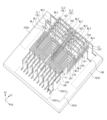
- 基板の上の第1積層構造体及び第2積層構造体であり、互いに平行に第1方向に延在される第1積層構造体及び第2積層構造体と、
前記第1及び第2積層構造体上の第1配線及び第2配線と、を含み、
前記第1及び第2積層構造体の各々は、
垂直方向に積層された複数の半導体パターンであり、各々が、前記第1方向と交差する第2方向に延在される複数の半導体パターンと、
垂直方向に積層されて前記複数の半導体パターンと連結された複数の導電ラインであり、各々が前記第1方向に延在される複数の導電ラインと、
前記複数の半導体パターンと隣接して垂直方向に延在されるゲート電極と、を含み、
前記第1積層構造体の前記複数の導電ラインは、第1導電ラインを含み、
前記第2積層構造体の前記複数の導電ラインは、前記第1導電ラインと同一なレベルに位置する第2導電ラインを含み、
前記第1配線は、前記第1及び第2導電ラインのうちの少なくとも1つと電気的に連結され、前記基板の外周部に向かって前記第1方向に引き出され、
前記第2配線は、前記第1及び第2積層構造体の前記ゲート電極のうちの少なくとも1つと電気的に連結され、前記基板の外周部に向かって前記第2方向に引き出される、半導体メモリ素子。 - 前記第1及び第2積層構造体上の第3配線をさらに含み、
前記第1配線は、前記第1導電ラインと電気的に連結され、
前記第3配線は、前記第2導電ラインと電気的に連結され、
前記第2配線は、前記第1及び第2積層構造体の前記ゲート電極と共通に連結される、請求項1に記載の半導体メモリ素子。 - 前記第2配線は、前記第2方向に延在され、
前記第2配線と共通に連結される前記ゲート電極は、前記第2方向に整列される、請求項2に記載の半導体メモリ素子。 - 前記第1及び第2積層構造体上の第3配線をさらに含み、
前記第1配線は、前記第1及び第2導電ラインと共通に連結され、
前記第2配線は、前記第1積層構造体の前記ゲート電極と電気的に連結され、
前記第3配線は、前記第2積層構造体の前記ゲート電極と電気的に連結される、請求項1に記載の半導体メモリ素子。 - 前記第1及び第2導電ラインと共通に接触する共通コンタクトをさらに含み、
前記第1配線は、前記共通コンタクトと電気的に連結される、請求項4に記載の半導体メモリ素子。 - 前記半導体パターンの各々は、第1不純物領域、第2不純物領域、及び前記第1及び第2不純物領域の間に介在されたチャネル領域を含み、
前記導電ラインの各々は、前記半導体パターンの各々の前記第1不純物領域と電気的に連結され、
前記ゲート電極の各々は、前記半導体パターンの前記チャネル領域に隣接する、請求項1に記載の半導体メモリ素子。 - 前記半導体パターンの各々は、第1不純物領域と前記導電ラインとの間に介在された終端膜をさらに含み、
前記終端膜は、前記チャネル領域の半導体元素より狭いバンドギャップを有する半導体元素を含む、請求項6に記載の半導体メモリ素子。 - 前記基板の前記外周部は、第1周辺回路領域及び第2周辺回路領域を含み、
前記第1配線は、前記第1方向に前記第1周辺回路領域に向かって延在されて、前記第1周辺回路領域上の第1周辺トランジスタと電気的に連結され、
前記第2配線は、前記第2方向に前記第2周辺回路領域に向かって延在されて、前記第2周辺回路領域上の第2周辺トランジスタと電気的に連結される、請求項1に記載の半導体メモリ素子。 - 前記第1及び第2導電ラインのうちの少なくとも1つと接触するコンタクトをさらに含み、
前記基板は、セル領域及びコンタクト領域を含み、
前記第1及び第2積層構造体の前記導電ラインは、前記セル領域から前記コンタクト領域に延長され、
前記コンタクトは、前記コンタクト領域上に配置され、
前記第1配線は、前記コンタクトと電気的に連結される、請求項1に記載の半導体メモリ素子。 - 前記基板は、セル領域及びコンタクト領域を含み、
前記第1及び第2積層構造体の前記導電ラインの各々は、
前記セル領域から前記コンタクト領域に水平方向に延在される配線部と、
前記コンタクト領域上で前記配線部から垂直方向に延在されるコンタクト部と、を含み、
前記第1配線は、前記第1及び第2導電ラインの前記コンタクト部のうちの少なくとも1つと電気的に連結される、請求項1に記載の半導体メモリ素子。 - セル領域及びコンタクト領域を含む基板と、
前記セル領域上で垂直方向に積層され、第1方向に延在される複数の半導体パターンであり、各々が第1不純物領域、第2不純物領域、及び前記第1及び第2不純物領域の間のチャネル領域を含む複数の半導体パターンと、
垂直方向に積層され、前記複数の半導体パターンの前記第1不純物領域と連結される複数の第1導電ラインであり、前記セル領域から前記コンタクト領域に、前記第1方向と交差する第2方向に延長された複数の第1導電ラインと、
前記複数の半導体パターンの各々の前記第2不純物領域と連結されるキャパシターと、
前記コンタクト領域上の前記複数の第1導電ラインと接触する複数のコンタクトであり、前記第2方向に整列された複数のコンタクトと、
前記複数のコンタクトと電気的に連結される複数の配線と、を含み、
前記複数のコンタクトは、第1コンタクト及び前記第1コンタクトより前記セル領域にさらに近い第2コンタクトを含み、
前記第2コンタクトの底面のレベルは、前記第1コンタクトの底面のレベルより高く、
前記複数の配線は、それぞれ前記第1コンタクト及び前記第2コンタクトと電気的に連結される第1配線及び第2配線を含み、
前記第1配線及び第2配線は、前記基板の外周部に向かって前記第2方向に引き出される、半導体メモリ素子。 - 前記第1コンタクトと接触する前記第1導電ラインは、前記コンタクト領域上で第1長さを有し、
前記第2コンタクトと接触する前記第1導電ラインは、前記コンタクト領域上で第2長さを有し、
前記第1長さは、前記第2長さより大きい、請求項11に記載の半導体メモリ素子。 - 前記基板の周辺回路領域上の第1下部配線及び第2下部配線、をさらに含み、
前記第1及び第2下部配線は、それぞれ、前記第1配線及び前記第2配線と電気的に連結され、
前記第1及び第2下部配線は、各々第1端及び第2端を含み、
前記第2端は、前記第1端より前記コンタクト領域に近い、請求項11に記載の半導体メモリ素子。 - 前記複数の半導体パターンの各々の前記チャネル領域と隣接して垂直方向に延在される第2導電ラインと、
前記第2導電ラインと電気的に連結される第3配線と、をさらに含み、
前記基板は、第1及び第2周辺回路領域をさらに含み、
前記第1及び第2配線は、前記第1周辺回路領域の上に延長され、前記第3配線は、前記第2周辺回路領域の上に延長される、請求項11に記載の半導体メモリ素子。
Applications Claiming Priority (4)
| Application Number | Priority Date | Filing Date | Title |
|---|---|---|---|
| US201862629335P | 2018-02-12 | 2018-02-12 | |
| US62/629,335 | 2018-02-12 | ||
| KR10-2018-0058523 | 2018-05-23 | ||
| KR1020180058523A KR102494114B1 (ko) | 2018-02-12 | 2018-05-23 | 반도체 메모리 소자 |
Publications (2)
| Publication Number | Publication Date |
|---|---|
| JP2019140382A JP2019140382A (ja) | 2019-08-22 |
| JP7338975B2 true JP7338975B2 (ja) | 2023-09-05 |
Family
ID=65279422
Family Applications (1)
| Application Number | Title | Priority Date | Filing Date |
|---|---|---|---|
| JP2019004399A Active JP7338975B2 (ja) | 2018-02-12 | 2019-01-15 | 半導体メモリ素子 |
Country Status (4)
| Country | Link |
|---|---|
| US (2) | US10910378B2 (ja) |
| EP (1) | EP3534401A3 (ja) |
| JP (1) | JP7338975B2 (ja) |
| CN (1) | CN110164867B (ja) |
Families Citing this family (16)
| Publication number | Priority date | Publication date | Assignee | Title |
|---|---|---|---|---|
| KR102639721B1 (ko) * | 2018-04-13 | 2024-02-26 | 삼성전자주식회사 | 3차원 반도체 메모리 장치 |
| KR102634614B1 (ko) | 2019-07-12 | 2024-02-08 | 에스케이하이닉스 주식회사 | 수직형 메모리 장치 |
| JP2021048298A (ja) * | 2019-09-19 | 2021-03-25 | キオクシア株式会社 | 半導体記憶装置及び半導体記憶装置の製造方法 |
| US11239238B2 (en) | 2019-10-29 | 2022-02-01 | Intel Corporation | Thin film transistor based memory cells on both sides of a layer of logic devices |
| US11335686B2 (en) | 2019-10-31 | 2022-05-17 | Intel Corporation | Transistors with back-side contacts to create three dimensional memory and logic |
| KR20210056778A (ko) | 2019-11-11 | 2021-05-20 | 삼성전자주식회사 | 집적회로 소자 및 그 제조 방법 |
| US11257822B2 (en) * | 2019-11-21 | 2022-02-22 | Intel Corporation | Three-dimensional nanoribbon-based dynamic random-access memory |
| KR20210063111A (ko) | 2019-11-22 | 2021-06-01 | 삼성전자주식회사 | 반도체 메모리 소자 및 그 제조 방법 |
| US11056492B1 (en) | 2019-12-23 | 2021-07-06 | Intel Corporation | Dense memory arrays utilizing access transistors with back-side contacts |
| KR20210090929A (ko) * | 2020-01-13 | 2021-07-21 | 에스케이하이닉스 주식회사 | 반도체 장치 및 그의 제조 방법 |
| US11087832B1 (en) | 2020-03-02 | 2021-08-10 | Intel Corporation | Three-dimensional nanoribbon-based static random-access memory |
| US11094699B1 (en) * | 2020-05-28 | 2021-08-17 | Micron Technology, Inc. | Apparatuses including stacked horizontal capacitor structures and related methods, memory devices, and electronic systems |
| KR20220026654A (ko) | 2020-08-25 | 2022-03-07 | 삼성전자주식회사 | 3차원 반도체 메모리 장치 |
| KR20230012623A (ko) * | 2020-09-02 | 2023-01-26 | 양쯔 메모리 테크놀로지스 씨오., 엘티디. | 반도체 디바이스에서 온칩 커패시터 구조를 형성하기 위한 방법 |
| JP2023001826A (ja) | 2021-06-21 | 2023-01-06 | キオクシア株式会社 | 半導体記憶装置 |
| CN117545270A (zh) * | 2022-07-27 | 2024-02-09 | 长鑫存储技术有限公司 | 半导体结构及其形成方法 |
Citations (5)
| Publication number | Priority date | Publication date | Assignee | Title |
|---|---|---|---|---|
| JP2003124476A (ja) | 1994-09-13 | 2003-04-25 | Toshiba Corp | 半導体装置及びその製造方法 |
| US20120231619A1 (en) | 2011-03-08 | 2012-09-13 | Samsung Electronics Co., Ltd. | Method of fabricating and semiconductor memory device using the same |
| JP2016526782A (ja) | 2013-07-01 | 2016-09-05 | マイクロン テクノロジー, インク. | 階段構造を含む半導体デバイスおよびこれに関連する方法 |
| US20170053906A1 (en) | 2015-08-23 | 2017-02-23 | Monolithic 3D Inc. | Semiconductor memory device and structure |
| US20170117291A1 (en) | 2015-10-24 | 2017-04-27 | Monolithic 3D Inc. | Semiconductor memory device, structure and methods |
Family Cites Families (20)
| Publication number | Priority date | Publication date | Assignee | Title |
|---|---|---|---|---|
| TW406419B (en) * | 1998-01-15 | 2000-09-21 | Siemens Ag | Memory-cells arrangement and its production method |
| JP2003234419A (ja) * | 2002-02-08 | 2003-08-22 | Mitsubishi Electric Corp | 半導体装置の製造方法およびその方法により製造された半導体装置 |
| KR100476694B1 (ko) * | 2002-11-07 | 2005-03-17 | 삼성전자주식회사 | 반도체 장치의 퓨즈 구조물 및 그 제조 방법 |
| US20050275006A1 (en) | 2004-05-25 | 2005-12-15 | Ming Tang | [multi-gate dram with deep-trench capacitor and fabrication thereof] |
| KR100688554B1 (ko) * | 2005-06-23 | 2007-03-02 | 삼성전자주식회사 | 파워 디커플링 커패시터를 포함하는 반도체 메모리 소자 |
| KR101527193B1 (ko) * | 2008-12-10 | 2015-06-08 | 삼성전자주식회사 | 반도체 소자 및 그의 셀 블록 배치 방법 |
| WO2010104918A1 (en) * | 2009-03-10 | 2010-09-16 | Contour Semiconductor, Inc. | Three-dimensional memory array comprising vertical switches having three terminals |
| KR20120092483A (ko) | 2011-02-11 | 2012-08-21 | 삼성전자주식회사 | 3차원 반도체 장치 및 그 제조 방법 |
| US8357964B1 (en) | 2011-09-07 | 2013-01-22 | Rexchip Electronics Corporation | Three-dimensional dynamic random access memory with an ancillary electrode structure |
| US9023723B2 (en) | 2012-05-31 | 2015-05-05 | Applied Materials, Inc. | Method of fabricating a gate-all-around word line for a vertical channel DRAM |
| KR20140026894A (ko) | 2012-08-23 | 2014-03-06 | 에스케이하이닉스 주식회사 | 3차원 적층형 메모리 장치 |
| US8902663B1 (en) | 2013-03-11 | 2014-12-02 | Monolithic 3D Inc. | Method of maintaining a memory state |
| CH708282A1 (de) * | 2013-07-10 | 2015-01-15 | Capartis Ag | Kunststoff-Behälter mit Drehverschluss. |
| US9570459B2 (en) * | 2013-07-10 | 2017-02-14 | Unity Semiconductor Corporation | Vertical gate NAND memory devices |
| US20150019802A1 (en) | 2013-07-11 | 2015-01-15 | Qualcomm Incorporated | Monolithic three dimensional (3d) random access memory (ram) array architecture with bitcell and logic partitioning |
| US20160268290A1 (en) * | 2015-03-11 | 2016-09-15 | Kabushiki Kaisha Toshiba | Method of manufacturing semiconductor device and semiconductor device |
| US9806088B2 (en) * | 2016-02-15 | 2017-10-31 | Toshiba Memory Corporation | Semiconductor memory device having memory cells arranged three-dimensionally and method of manufacturing the same |
| JP6517720B2 (ja) | 2016-03-16 | 2019-05-22 | 東芝メモリ株式会社 | 半導体記憶装置 |
| US20170278858A1 (en) | 2016-03-22 | 2017-09-28 | Schiltron Corporation | Monolithic 3-d dynamic memory and method |
| JP6645940B2 (ja) * | 2016-09-20 | 2020-02-14 | キオクシア株式会社 | 不揮発性半導体記憶装置 |
-
2019
- 2019-01-15 JP JP2019004399A patent/JP7338975B2/ja active Active
- 2019-02-01 EP EP19155115.9A patent/EP3534401A3/en active Pending
- 2019-02-03 CN CN201910108496.7A patent/CN110164867B/zh active Active
- 2019-02-06 US US16/268,748 patent/US10910378B2/en active Active
-
2020
- 2020-12-18 US US17/126,195 patent/US11569239B2/en active Active
Patent Citations (5)
| Publication number | Priority date | Publication date | Assignee | Title |
|---|---|---|---|---|
| JP2003124476A (ja) | 1994-09-13 | 2003-04-25 | Toshiba Corp | 半導体装置及びその製造方法 |
| US20120231619A1 (en) | 2011-03-08 | 2012-09-13 | Samsung Electronics Co., Ltd. | Method of fabricating and semiconductor memory device using the same |
| JP2016526782A (ja) | 2013-07-01 | 2016-09-05 | マイクロン テクノロジー, インク. | 階段構造を含む半導体デバイスおよびこれに関連する方法 |
| US20170053906A1 (en) | 2015-08-23 | 2017-02-23 | Monolithic 3D Inc. | Semiconductor memory device and structure |
| US20170117291A1 (en) | 2015-10-24 | 2017-04-27 | Monolithic 3D Inc. | Semiconductor memory device, structure and methods |
Also Published As
| Publication number | Publication date |
|---|---|
| US20210143154A1 (en) | 2021-05-13 |
| CN110164867A (zh) | 2019-08-23 |
| US20190252386A1 (en) | 2019-08-15 |
| CN110164867B (zh) | 2023-09-29 |
| JP2019140382A (ja) | 2019-08-22 |
| EP3534401A3 (en) | 2020-01-08 |
| US11569239B2 (en) | 2023-01-31 |
| US10910378B2 (en) | 2021-02-02 |
| EP3534401A2 (en) | 2019-09-04 |
Similar Documents
| Publication | Publication Date | Title |
|---|---|---|
| JP7338975B2 (ja) | 半導体メモリ素子 | |
| CN109616474B (zh) | 半导体存储器件 | |
| KR102638741B1 (ko) | 반도체 메모리 소자 | |
| US11374008B2 (en) | Semiconductor memory devices and methods of fabricating the same | |
| KR102630024B1 (ko) | 반도체 메모리 소자 | |
| KR102618309B1 (ko) | 반도체 장치 및 그 제조방법 | |
| TW202230630A (zh) | 半導體記憶體元件 | |
| JP7311254B2 (ja) | 半導体メモリ素子 | |
| KR102494114B1 (ko) | 반도체 메모리 소자 | |
| US11495542B2 (en) | Semiconductor memory device and method of fabricating the same | |
| US11081499B2 (en) | Nonvolatile memory device and method for fabricating the same | |
| KR20210050630A (ko) | 반도체 메모리 소자 | |
| US11437380B2 (en) | Semiconductor memory device and method of manufacturing the same | |
| TWI817447B (zh) | 三維記憶體陣列之結構 | |
| US11594550B2 (en) | Nonvolatile memory device with h-shaped blocks and method of fabricating the same | |
| KR20230154692A (ko) | 반도체 장치 | |
| KR20230142405A (ko) | 반도체 장치 | |
| KR20240050241A (ko) | 반도체 메모리 장치 | |
| KR20220157142A (ko) | 반도체 메모리 장치 및 그 제조 방법 |
Legal Events
| Date | Code | Title | Description |
|---|---|---|---|
| A621 | Written request for application examination |
Free format text: JAPANESE INTERMEDIATE CODE: A621 Effective date: 20220104 |
|
| A977 | Report on retrieval |
Free format text: JAPANESE INTERMEDIATE CODE: A971007 Effective date: 20230210 |
|
| A131 | Notification of reasons for refusal |
Free format text: JAPANESE INTERMEDIATE CODE: A131 Effective date: 20230221 |
|
| A521 | Request for written amendment filed |
Free format text: JAPANESE INTERMEDIATE CODE: A523 Effective date: 20230510 |
|
| TRDD | Decision of grant or rejection written | ||
| A01 | Written decision to grant a patent or to grant a registration (utility model) |
Free format text: JAPANESE INTERMEDIATE CODE: A01 Effective date: 20230815 |
|
| A61 | First payment of annual fees (during grant procedure) |
Free format text: JAPANESE INTERMEDIATE CODE: A61 Effective date: 20230824 |
|
| R150 | Certificate of patent or registration of utility model |
Ref document number: 7338975 Country of ref document: JP Free format text: JAPANESE INTERMEDIATE CODE: R150 |