JP7186732B2 - 表示装置 - Google Patents
表示装置 Download PDFInfo
- Publication number
- JP7186732B2 JP7186732B2 JP2019571122A JP2019571122A JP7186732B2 JP 7186732 B2 JP7186732 B2 JP 7186732B2 JP 2019571122 A JP2019571122 A JP 2019571122A JP 2019571122 A JP2019571122 A JP 2019571122A JP 7186732 B2 JP7186732 B2 JP 7186732B2
- Authority
- JP
- Japan
- Prior art keywords
- insulator
- oxide
- conductor
- region
- transistor
- Prior art date
- Legal status (The legal status is an assumption and is not a legal conclusion. Google has not performed a legal analysis and makes no representation as to the accuracy of the status listed.)
- Active
Links
- 239000012212 insulator Substances 0.000 claims description 1048
- 239000004020 conductor Substances 0.000 claims description 752
- 230000015572 biosynthetic process Effects 0.000 claims description 105
- 239000004973 liquid crystal related substance Substances 0.000 claims description 48
- 229910052710 silicon Inorganic materials 0.000 claims description 43
- 239000010703 silicon Substances 0.000 claims description 43
- ZOXJGFHDIHLPTG-UHFFFAOYSA-N Boron Chemical compound [B] ZOXJGFHDIHLPTG-UHFFFAOYSA-N 0.000 claims description 17
- 229910052796 boron Inorganic materials 0.000 claims description 17
- OAICVXFJPJFONN-UHFFFAOYSA-N Phosphorus Chemical compound [P] OAICVXFJPJFONN-UHFFFAOYSA-N 0.000 claims description 15
- 239000011574 phosphorus Substances 0.000 claims description 15
- 229910052698 phosphorus Inorganic materials 0.000 claims description 15
- 239000010408 film Substances 0.000 description 566
- 239000010410 layer Substances 0.000 description 474
- 238000000034 method Methods 0.000 description 313
- 229910052760 oxygen Inorganic materials 0.000 description 192
- 239000001301 oxygen Substances 0.000 description 189
- QVGXLLKOCUKJST-UHFFFAOYSA-N atomic oxygen Chemical compound [O] QVGXLLKOCUKJST-UHFFFAOYSA-N 0.000 description 187
- 230000006870 function Effects 0.000 description 160
- 239000000463 material Substances 0.000 description 151
- 239000004065 semiconductor Substances 0.000 description 123
- 238000004519 manufacturing process Methods 0.000 description 121
- 239000000758 substrate Substances 0.000 description 114
- 238000010438 heat treatment Methods 0.000 description 104
- 239000001257 hydrogen Substances 0.000 description 100
- 229910052739 hydrogen Inorganic materials 0.000 description 100
- UFHFLCQGNIYNRP-UHFFFAOYSA-N Hydrogen Chemical compound [H][H] UFHFLCQGNIYNRP-UHFFFAOYSA-N 0.000 description 89
- 229910044991 metal oxide Inorganic materials 0.000 description 87
- 239000012535 impurity Substances 0.000 description 82
- 150000004706 metal oxides Chemical class 0.000 description 78
- 238000004544 sputter deposition Methods 0.000 description 61
- 238000000231 atomic layer deposition Methods 0.000 description 60
- IJGRMHOSHXDMSA-UHFFFAOYSA-N Atomic nitrogen Chemical compound N#N IJGRMHOSHXDMSA-UHFFFAOYSA-N 0.000 description 58
- 229910052751 metal Inorganic materials 0.000 description 57
- 239000003990 capacitor Substances 0.000 description 49
- 239000002184 metal Substances 0.000 description 49
- 229910052782 aluminium Inorganic materials 0.000 description 48
- 238000009792 diffusion process Methods 0.000 description 47
- 238000005401 electroluminescence Methods 0.000 description 47
- XAGFODPZIPBFFR-UHFFFAOYSA-N aluminium Chemical compound [Al] XAGFODPZIPBFFR-UHFFFAOYSA-N 0.000 description 46
- 239000007789 gas Substances 0.000 description 46
- 239000011701 zinc Substances 0.000 description 45
- 125000004430 oxygen atom Chemical group O* 0.000 description 44
- VYPSYNLAJGMNEJ-UHFFFAOYSA-N silicon dioxide Inorganic materials O=[Si]=O VYPSYNLAJGMNEJ-UHFFFAOYSA-N 0.000 description 44
- 238000005229 chemical vapour deposition Methods 0.000 description 43
- 229910052814 silicon oxide Inorganic materials 0.000 description 43
- 239000000126 substance Substances 0.000 description 43
- XLYOFNOQVPJJNP-UHFFFAOYSA-N water Substances O XLYOFNOQVPJJNP-UHFFFAOYSA-N 0.000 description 43
- 229910001868 water Inorganic materials 0.000 description 43
- XUIMIQQOPSSXEZ-UHFFFAOYSA-N Silicon Chemical compound [Si] XUIMIQQOPSSXEZ-UHFFFAOYSA-N 0.000 description 41
- 239000002019 doping agent Substances 0.000 description 39
- 229910052735 hafnium Inorganic materials 0.000 description 36
- 125000004429 atom Chemical group 0.000 description 34
- -1 etc.) Substances 0.000 description 33
- TWNQGVIAIRXVLR-UHFFFAOYSA-N oxo(oxoalumanyloxy)alumane Chemical compound O=[Al]O[Al]=O TWNQGVIAIRXVLR-UHFFFAOYSA-N 0.000 description 32
- HCHKCACWOHOZIP-UHFFFAOYSA-N Zinc Chemical compound [Zn] HCHKCACWOHOZIP-UHFFFAOYSA-N 0.000 description 30
- VBJZVLUMGGDVMO-UHFFFAOYSA-N hafnium atom Chemical group [Hf] VBJZVLUMGGDVMO-UHFFFAOYSA-N 0.000 description 30
- 229910052799 carbon Inorganic materials 0.000 description 29
- 230000008569 process Effects 0.000 description 29
- 239000012298 atmosphere Substances 0.000 description 28
- 229910052757 nitrogen Inorganic materials 0.000 description 28
- PXHVJJICTQNCMI-UHFFFAOYSA-N Nickel Chemical group [Ni] PXHVJJICTQNCMI-UHFFFAOYSA-N 0.000 description 26
- 238000001312 dry etching Methods 0.000 description 26
- OKTJSMMVPCPJKN-UHFFFAOYSA-N Carbon Chemical compound [C] OKTJSMMVPCPJKN-UHFFFAOYSA-N 0.000 description 25
- 229910052581 Si3N4 Inorganic materials 0.000 description 25
- 238000004549 pulsed laser deposition Methods 0.000 description 25
- HQVNEWCFYHHQES-UHFFFAOYSA-N silicon nitride Chemical compound N12[Si]34N5[Si]62N3[Si]51N64 HQVNEWCFYHHQES-UHFFFAOYSA-N 0.000 description 25
- 238000001451 molecular beam epitaxy Methods 0.000 description 24
- YCKRFDGAMUMZLT-UHFFFAOYSA-N Fluorine atom Chemical compound [F] YCKRFDGAMUMZLT-UHFFFAOYSA-N 0.000 description 22
- 229910052731 fluorine Inorganic materials 0.000 description 22
- 239000011737 fluorine Substances 0.000 description 22
- 238000002347 injection Methods 0.000 description 22
- 239000007924 injection Substances 0.000 description 22
- 238000005530 etching Methods 0.000 description 21
- 238000012545 processing Methods 0.000 description 21
- 238000001039 wet etching Methods 0.000 description 21
- 230000007547 defect Effects 0.000 description 20
- RTAQQCXQSZGOHL-UHFFFAOYSA-N Titanium Chemical group [Ti] RTAQQCXQSZGOHL-UHFFFAOYSA-N 0.000 description 19
- 229910052719 titanium Inorganic materials 0.000 description 19
- 239000010936 titanium Chemical group 0.000 description 19
- WFKWXMTUELFFGS-UHFFFAOYSA-N tungsten Chemical group [W] WFKWXMTUELFFGS-UHFFFAOYSA-N 0.000 description 18
- 229910052721 tungsten Inorganic materials 0.000 description 18
- 239000010937 tungsten Chemical group 0.000 description 18
- 229910007541 Zn O Inorganic materials 0.000 description 17
- 229910052738 indium Inorganic materials 0.000 description 17
- APFVFJFRJDLVQX-UHFFFAOYSA-N indium atom Chemical compound [In] APFVFJFRJDLVQX-UHFFFAOYSA-N 0.000 description 16
- 229910052741 iridium Inorganic materials 0.000 description 16
- 150000004767 nitrides Chemical class 0.000 description 16
- 150000002894 organic compounds Chemical class 0.000 description 16
- 230000035699 permeability Effects 0.000 description 16
- 229910052715 tantalum Inorganic materials 0.000 description 16
- GUVRBAGPIYLISA-UHFFFAOYSA-N tantalum atom Chemical group [Ta] GUVRBAGPIYLISA-UHFFFAOYSA-N 0.000 description 16
- RYGMFSIKBFXOCR-UHFFFAOYSA-N Copper Chemical compound [Cu] RYGMFSIKBFXOCR-UHFFFAOYSA-N 0.000 description 15
- NRTOMJZYCJJWKI-UHFFFAOYSA-N Titanium nitride Chemical compound [Ti]#N NRTOMJZYCJJWKI-UHFFFAOYSA-N 0.000 description 15
- GKOZUEZYRPOHIO-UHFFFAOYSA-N iridium atom Chemical compound [Ir] GKOZUEZYRPOHIO-UHFFFAOYSA-N 0.000 description 15
- 229910052707 ruthenium Inorganic materials 0.000 description 15
- 229910052725 zinc Inorganic materials 0.000 description 15
- 238000004140 cleaning Methods 0.000 description 14
- 150000001875 compounds Chemical class 0.000 description 14
- 239000013078 crystal Substances 0.000 description 14
- 230000005525 hole transport Effects 0.000 description 14
- 230000004888 barrier function Effects 0.000 description 13
- 229910052759 nickel Inorganic materials 0.000 description 13
- BASFCYQUMIYNBI-UHFFFAOYSA-N platinum Chemical compound [Pt] BASFCYQUMIYNBI-UHFFFAOYSA-N 0.000 description 13
- 239000002096 quantum dot Substances 0.000 description 13
- 238000004891 communication Methods 0.000 description 12
- 229910052802 copper Inorganic materials 0.000 description 12
- 239000010949 copper Substances 0.000 description 12
- 229910052746 lanthanum Inorganic materials 0.000 description 12
- FZLIPJUXYLNCLC-UHFFFAOYSA-N lanthanum atom Chemical group [La] FZLIPJUXYLNCLC-UHFFFAOYSA-N 0.000 description 12
- 239000011777 magnesium Chemical group 0.000 description 12
- 230000003287 optical effect Effects 0.000 description 12
- FYYHWMGAXLPEAU-UHFFFAOYSA-N Magnesium Chemical group [Mg] FYYHWMGAXLPEAU-UHFFFAOYSA-N 0.000 description 11
- KJTLSVCANCCWHF-UHFFFAOYSA-N Ruthenium Chemical compound [Ru] KJTLSVCANCCWHF-UHFFFAOYSA-N 0.000 description 11
- 239000000370 acceptor Substances 0.000 description 11
- 230000000694 effects Effects 0.000 description 11
- 229910052733 gallium Inorganic materials 0.000 description 11
- 150000002431 hydrogen Chemical class 0.000 description 11
- 229910052749 magnesium Chemical group 0.000 description 11
- GYHNNYVSQQEPJS-UHFFFAOYSA-N Gallium Chemical compound [Ga] GYHNNYVSQQEPJS-UHFFFAOYSA-N 0.000 description 10
- 230000005684 electric field Effects 0.000 description 10
- 229910000449 hafnium oxide Inorganic materials 0.000 description 10
- WIHZLLGSGQNAGK-UHFFFAOYSA-N hafnium(4+);oxygen(2-) Chemical compound [O-2].[O-2].[Hf+4] WIHZLLGSGQNAGK-UHFFFAOYSA-N 0.000 description 10
- 238000001459 lithography Methods 0.000 description 10
- 125000002524 organometallic group Chemical group 0.000 description 10
- 239000002356 single layer Substances 0.000 description 10
- MWUXSHHQAYIFBG-UHFFFAOYSA-N Nitric oxide Chemical compound O=[N] MWUXSHHQAYIFBG-UHFFFAOYSA-N 0.000 description 9
- QCWXUUIWCKQGHC-UHFFFAOYSA-N Zirconium Chemical group [Zr] QCWXUUIWCKQGHC-UHFFFAOYSA-N 0.000 description 9
- 238000004380 ashing Methods 0.000 description 9
- 239000000969 carrier Substances 0.000 description 9
- PMHQVHHXPFUNSP-UHFFFAOYSA-M copper(1+);methylsulfanylmethane;bromide Chemical compound Br[Cu].CSC PMHQVHHXPFUNSP-UHFFFAOYSA-M 0.000 description 9
- 230000007423 decrease Effects 0.000 description 9
- AJNVQOSZGJRYEI-UHFFFAOYSA-N digallium;oxygen(2-) Chemical compound [O-2].[O-2].[O-2].[Ga+3].[Ga+3] AJNVQOSZGJRYEI-UHFFFAOYSA-N 0.000 description 9
- 229910001195 gallium oxide Inorganic materials 0.000 description 9
- 239000011229 interlayer Substances 0.000 description 9
- 230000004048 modification Effects 0.000 description 9
- 238000012986 modification Methods 0.000 description 9
- 238000009832 plasma treatment Methods 0.000 description 9
- 239000011347 resin Substances 0.000 description 9
- 229920005989 resin Polymers 0.000 description 9
- 229910052712 strontium Inorganic materials 0.000 description 9
- MZLGASXMSKOWSE-UHFFFAOYSA-N tantalum nitride Chemical compound [Ta]#N MZLGASXMSKOWSE-UHFFFAOYSA-N 0.000 description 9
- 229910052726 zirconium Inorganic materials 0.000 description 9
- XEEYBQQBJWHFJM-UHFFFAOYSA-N Iron Chemical group [Fe] XEEYBQQBJWHFJM-UHFFFAOYSA-N 0.000 description 8
- ZOKXTWBITQBERF-UHFFFAOYSA-N Molybdenum Chemical group [Mo] ZOKXTWBITQBERF-UHFFFAOYSA-N 0.000 description 8
- 229910052783 alkali metal Inorganic materials 0.000 description 8
- 150000001340 alkali metals Chemical class 0.000 description 8
- 229910045601 alloy Inorganic materials 0.000 description 8
- 239000000956 alloy Substances 0.000 description 8
- 238000010586 diagram Methods 0.000 description 8
- 230000005284 excitation Effects 0.000 description 8
- 125000004435 hydrogen atom Chemical group [H]* 0.000 description 8
- 150000002739 metals Chemical class 0.000 description 8
- 239000000203 mixture Substances 0.000 description 8
- 229910052750 molybdenum Inorganic materials 0.000 description 8
- 239000011733 molybdenum Chemical group 0.000 description 8
- 229920000642 polymer Polymers 0.000 description 8
- 230000035882 stress Effects 0.000 description 8
- CIOAGBVUUVVLOB-UHFFFAOYSA-N strontium atom Chemical compound [Sr] CIOAGBVUUVVLOB-UHFFFAOYSA-N 0.000 description 8
- 229910052727 yttrium Inorganic materials 0.000 description 8
- 239000007983 Tris buffer Substances 0.000 description 7
- 229910052784 alkaline earth metal Inorganic materials 0.000 description 7
- 150000001342 alkaline earth metals Chemical class 0.000 description 7
- 239000000460 chlorine Substances 0.000 description 7
- 239000003086 colorant Substances 0.000 description 7
- 239000002131 composite material Substances 0.000 description 7
- 239000000470 constituent Substances 0.000 description 7
- 150000002500 ions Chemical class 0.000 description 7
- 230000003647 oxidation Effects 0.000 description 7
- 238000007254 oxidation reaction Methods 0.000 description 7
- 229910001925 ruthenium oxide Inorganic materials 0.000 description 7
- WOCIAKWEIIZHES-UHFFFAOYSA-N ruthenium(iv) oxide Chemical compound O=[Ru]=O WOCIAKWEIIZHES-UHFFFAOYSA-N 0.000 description 7
- XKRFYHLGVUSROY-UHFFFAOYSA-N Argon Chemical compound [Ar] XKRFYHLGVUSROY-UHFFFAOYSA-N 0.000 description 6
- ATJFFYVFTNAWJD-UHFFFAOYSA-N Tin Chemical compound [Sn] ATJFFYVFTNAWJD-UHFFFAOYSA-N 0.000 description 6
- XLOMVQKBTHCTTD-UHFFFAOYSA-N Zinc monoxide Chemical compound [Zn]=O XLOMVQKBTHCTTD-UHFFFAOYSA-N 0.000 description 6
- 229910021417 amorphous silicon Inorganic materials 0.000 description 6
- 230000002950 deficient Effects 0.000 description 6
- 230000005281 excited state Effects 0.000 description 6
- 230000005669 field effect Effects 0.000 description 6
- 229910052732 germanium Inorganic materials 0.000 description 6
- GNPVGFCGXDBREM-UHFFFAOYSA-N germanium atom Chemical compound [Ge] GNPVGFCGXDBREM-UHFFFAOYSA-N 0.000 description 6
- 125000001072 heteroaryl group Chemical group 0.000 description 6
- 239000002159 nanocrystal Substances 0.000 description 6
- 239000012466 permeate Substances 0.000 description 6
- 229910052697 platinum Inorganic materials 0.000 description 6
- 229910021420 polycrystalline silicon Inorganic materials 0.000 description 6
- 229910052718 tin Inorganic materials 0.000 description 6
- VWQVUPCCIRVNHF-UHFFFAOYSA-N yttrium atom Chemical group [Y] VWQVUPCCIRVNHF-UHFFFAOYSA-N 0.000 description 6
- CUJRVFIICFDLGR-UHFFFAOYSA-N acetylacetonate Chemical compound CC(=O)[CH-]C(C)=O CUJRVFIICFDLGR-UHFFFAOYSA-N 0.000 description 5
- UQZIWOQVLUASCR-UHFFFAOYSA-N alumane;titanium Chemical compound [AlH3].[Ti] UQZIWOQVLUASCR-UHFFFAOYSA-N 0.000 description 5
- 229910052790 beryllium Inorganic materials 0.000 description 5
- ATBAMAFKBVZNFJ-UHFFFAOYSA-N beryllium atom Chemical group [Be] ATBAMAFKBVZNFJ-UHFFFAOYSA-N 0.000 description 5
- 230000006378 damage Effects 0.000 description 5
- 239000007788 liquid Substances 0.000 description 5
- 238000005498 polishing Methods 0.000 description 5
- 239000002243 precursor Substances 0.000 description 5
- 238000001004 secondary ion mass spectrometry Methods 0.000 description 5
- 229910052709 silver Inorganic materials 0.000 description 5
- 239000004332 silver Substances 0.000 description 5
- 238000002230 thermal chemical vapour deposition Methods 0.000 description 5
- 239000010409 thin film Substances 0.000 description 5
- 229910052720 vanadium Inorganic materials 0.000 description 5
- GPPXJZIENCGNKB-UHFFFAOYSA-N vanadium Chemical group [V]#[V] GPPXJZIENCGNKB-UHFFFAOYSA-N 0.000 description 5
- ZAMOUSCENKQFHK-UHFFFAOYSA-N Chlorine atom Chemical compound [Cl] ZAMOUSCENKQFHK-UHFFFAOYSA-N 0.000 description 4
- VYZAMTAEIAYCRO-UHFFFAOYSA-N Chromium Chemical compound [Cr] VYZAMTAEIAYCRO-UHFFFAOYSA-N 0.000 description 4
- 229910052779 Neodymium Inorganic materials 0.000 description 4
- BQCADISMDOOEFD-UHFFFAOYSA-N Silver Chemical compound [Ag] BQCADISMDOOEFD-UHFFFAOYSA-N 0.000 description 4
- XJHCXCQVJFPJIK-UHFFFAOYSA-M caesium fluoride Chemical compound [F-].[Cs+] XJHCXCQVJFPJIK-UHFFFAOYSA-M 0.000 description 4
- 229910052801 chlorine Inorganic materials 0.000 description 4
- 229910052804 chromium Inorganic materials 0.000 description 4
- 239000011651 chromium Substances 0.000 description 4
- 230000003111 delayed effect Effects 0.000 description 4
- 238000000151 deposition Methods 0.000 description 4
- 230000006866 deterioration Effects 0.000 description 4
- 239000011521 glass Substances 0.000 description 4
- PCHJSUWPFVWCPO-UHFFFAOYSA-N gold Chemical compound [Au] PCHJSUWPFVWCPO-UHFFFAOYSA-N 0.000 description 4
- 229910052737 gold Inorganic materials 0.000 description 4
- 239000010931 gold Substances 0.000 description 4
- MILUBEOXRNEUHS-UHFFFAOYSA-N iridium(3+) Chemical compound [Ir+3] MILUBEOXRNEUHS-UHFFFAOYSA-N 0.000 description 4
- 229910052742 iron Inorganic materials 0.000 description 4
- WPBNNNQJVZRUHP-UHFFFAOYSA-L manganese(2+);methyl n-[[2-(methoxycarbonylcarbamothioylamino)phenyl]carbamothioyl]carbamate;n-[2-(sulfidocarbothioylamino)ethyl]carbamodithioate Chemical compound [Mn+2].[S-]C(=S)NCCNC([S-])=S.COC(=O)NC(=S)NC1=CC=CC=C1NC(=S)NC(=O)OC WPBNNNQJVZRUHP-UHFFFAOYSA-L 0.000 description 4
- QEFYFXOXNSNQGX-UHFFFAOYSA-N neodymium atom Chemical group [Nd] QEFYFXOXNSNQGX-UHFFFAOYSA-N 0.000 description 4
- 229910052758 niobium Inorganic materials 0.000 description 4
- 239000010955 niobium Substances 0.000 description 4
- GUCVJGMIXFAOAE-UHFFFAOYSA-N niobium atom Chemical compound [Nb] GUCVJGMIXFAOAE-UHFFFAOYSA-N 0.000 description 4
- 230000001590 oxidative effect Effects 0.000 description 4
- RVTZCBVAJQQJTK-UHFFFAOYSA-N oxygen(2-);zirconium(4+) Chemical compound [O-2].[O-2].[Zr+4] RVTZCBVAJQQJTK-UHFFFAOYSA-N 0.000 description 4
- 230000003071 parasitic effect Effects 0.000 description 4
- 230000000737 periodic effect Effects 0.000 description 4
- 229920003227 poly(N-vinyl carbazole) Polymers 0.000 description 4
- 229910052761 rare earth metal Inorganic materials 0.000 description 4
- 150000002910 rare earth metals Chemical class 0.000 description 4
- 238000000926 separation method Methods 0.000 description 4
- 238000012360 testing method Methods 0.000 description 4
- OGIDPMRJRNCKJF-UHFFFAOYSA-N titanium oxide Inorganic materials [Ti]=O OGIDPMRJRNCKJF-UHFFFAOYSA-N 0.000 description 4
- 229910001928 zirconium oxide Inorganic materials 0.000 description 4
- 229910052684 Cerium Inorganic materials 0.000 description 3
- MUBZPKHOEPUJKR-UHFFFAOYSA-N Oxalic acid Chemical compound OC(=O)C(O)=O MUBZPKHOEPUJKR-UHFFFAOYSA-N 0.000 description 3
- KDLHZDBZIXYQEI-UHFFFAOYSA-N Palladium Chemical compound [Pd] KDLHZDBZIXYQEI-UHFFFAOYSA-N 0.000 description 3
- 239000004983 Polymer Dispersed Liquid Crystal Substances 0.000 description 3
- GWEVSGVZZGPLCZ-UHFFFAOYSA-N Titan oxide Chemical compound O=[Ti]=O GWEVSGVZZGPLCZ-UHFFFAOYSA-N 0.000 description 3
- 230000001133 acceleration Effects 0.000 description 3
- 125000005595 acetylacetonate group Chemical group 0.000 description 3
- 238000004458 analytical method Methods 0.000 description 3
- 229910052786 argon Inorganic materials 0.000 description 3
- ZMIGMASIKSOYAM-UHFFFAOYSA-N cerium Chemical group [Ce][Ce][Ce][Ce][Ce][Ce][Ce][Ce][Ce][Ce][Ce][Ce][Ce][Ce][Ce][Ce][Ce][Ce][Ce][Ce][Ce][Ce][Ce][Ce][Ce][Ce][Ce][Ce][Ce][Ce][Ce][Ce][Ce][Ce][Ce][Ce][Ce][Ce] ZMIGMASIKSOYAM-UHFFFAOYSA-N 0.000 description 3
- 238000006243 chemical reaction Methods 0.000 description 3
- 238000000576 coating method Methods 0.000 description 3
- 238000004040 coloring Methods 0.000 description 3
- 238000012937 correction Methods 0.000 description 3
- 125000006575 electron-withdrawing group Chemical group 0.000 description 3
- 238000000295 emission spectrum Methods 0.000 description 3
- 238000000605 extraction Methods 0.000 description 3
- 150000002390 heteroarenes Chemical class 0.000 description 3
- 229910003437 indium oxide Inorganic materials 0.000 description 3
- PJXISJQVUVHSOJ-UHFFFAOYSA-N indium(iii) oxide Chemical compound [O-2].[O-2].[O-2].[In+3].[In+3] PJXISJQVUVHSOJ-UHFFFAOYSA-N 0.000 description 3
- AMGQUBHHOARCQH-UHFFFAOYSA-N indium;oxotin Chemical compound [In].[Sn]=O AMGQUBHHOARCQH-UHFFFAOYSA-N 0.000 description 3
- 239000011261 inert gas Substances 0.000 description 3
- 239000011810 insulating material Substances 0.000 description 3
- 238000005468 ion implantation Methods 0.000 description 3
- 238000002955 isolation Methods 0.000 description 3
- 229910000476 molybdenum oxide Inorganic materials 0.000 description 3
- 125000004433 nitrogen atom Chemical group N* 0.000 description 3
- QGLKJKCYBOYXKC-UHFFFAOYSA-N nonaoxidotritungsten Chemical compound O=[W]1(=O)O[W](=O)(=O)O[W](=O)(=O)O1 QGLKJKCYBOYXKC-UHFFFAOYSA-N 0.000 description 3
- PQQKPALAQIIWST-UHFFFAOYSA-N oxomolybdenum Chemical compound [Mo]=O PQQKPALAQIIWST-UHFFFAOYSA-N 0.000 description 3
- 229920005591 polysilicon Polymers 0.000 description 3
- 150000003252 quinoxalines Chemical class 0.000 description 3
- 239000002994 raw material Substances 0.000 description 3
- FZHAPNGMFPVSLP-UHFFFAOYSA-N silanamine Chemical class [SiH3]N FZHAPNGMFPVSLP-UHFFFAOYSA-N 0.000 description 3
- 239000000243 solution Substances 0.000 description 3
- 238000012546 transfer Methods 0.000 description 3
- 229910001930 tungsten oxide Inorganic materials 0.000 description 3
- 238000007738 vacuum evaporation Methods 0.000 description 3
- 239000011787 zinc oxide Substances 0.000 description 3
- IYZMXHQDXZKNCY-UHFFFAOYSA-N 1-n,1-n-diphenyl-4-n,4-n-bis[4-(n-phenylanilino)phenyl]benzene-1,4-diamine Chemical compound C1=CC=CC=C1N(C=1C=CC(=CC=1)N(C=1C=CC(=CC=1)N(C=1C=CC=CC=1)C=1C=CC=CC=1)C=1C=CC(=CC=1)N(C=1C=CC=CC=1)C=1C=CC=CC=1)C1=CC=CC=C1 IYZMXHQDXZKNCY-UHFFFAOYSA-N 0.000 description 2
- QGZKDVFQNNGYKY-UHFFFAOYSA-N Ammonia Chemical compound N QGZKDVFQNNGYKY-UHFFFAOYSA-N 0.000 description 2
- OYPRJOBELJOOCE-UHFFFAOYSA-N Calcium Chemical compound [Ca] OYPRJOBELJOOCE-UHFFFAOYSA-N 0.000 description 2
- KRHYYFGTRYWZRS-UHFFFAOYSA-N Fluorane Chemical compound F KRHYYFGTRYWZRS-UHFFFAOYSA-N 0.000 description 2
- YLQBMQCUIZJEEH-UHFFFAOYSA-N Furan Chemical group C=1C=COC=1 YLQBMQCUIZJEEH-UHFFFAOYSA-N 0.000 description 2
- OAKJQQAXSVQMHS-UHFFFAOYSA-N Hydrazine Chemical compound NN OAKJQQAXSVQMHS-UHFFFAOYSA-N 0.000 description 2
- CBENFWSGALASAD-UHFFFAOYSA-N Ozone Chemical compound [O-][O+]=O CBENFWSGALASAD-UHFFFAOYSA-N 0.000 description 2
- YNPNZTXNASCQKK-UHFFFAOYSA-N Phenanthrene Natural products C1=CC=C2C3=CC=CC=C3C=CC2=C1 YNPNZTXNASCQKK-UHFFFAOYSA-N 0.000 description 2
- NBIIXXVUZAFLBC-UHFFFAOYSA-N Phosphoric acid Chemical compound OP(O)(O)=O NBIIXXVUZAFLBC-UHFFFAOYSA-N 0.000 description 2
- 229920001609 Poly(3,4-ethylenedioxythiophene) Polymers 0.000 description 2
- JUJWROOIHBZHMG-UHFFFAOYSA-N Pyridine Chemical group C1=CC=NC=C1 JUJWROOIHBZHMG-UHFFFAOYSA-N 0.000 description 2
- SMWDFEZZVXVKRB-UHFFFAOYSA-N Quinoline Chemical compound N1=CC=CC2=CC=CC=C21 SMWDFEZZVXVKRB-UHFFFAOYSA-N 0.000 description 2
- NINIDFKCEFEMDL-UHFFFAOYSA-N Sulfur Chemical compound [S] NINIDFKCEFEMDL-UHFFFAOYSA-N 0.000 description 2
- 238000004833 X-ray photoelectron spectroscopy Methods 0.000 description 2
- DGEZNRSVGBDHLK-UHFFFAOYSA-N [1,10]phenanthroline Chemical compound C1=CN=C2C3=NC=CC=C3C=CC2=C1 DGEZNRSVGBDHLK-UHFFFAOYSA-N 0.000 description 2
- XHCLAFWTIXFWPH-UHFFFAOYSA-N [O-2].[O-2].[O-2].[O-2].[O-2].[V+5].[V+5] Chemical compound [O-2].[O-2].[O-2].[O-2].[O-2].[V+5].[V+5] XHCLAFWTIXFWPH-UHFFFAOYSA-N 0.000 description 2
- 230000009471 action Effects 0.000 description 2
- 150000001454 anthracenes Chemical class 0.000 description 2
- 230000003190 augmentative effect Effects 0.000 description 2
- QVQLCTNNEUAWMS-UHFFFAOYSA-N barium oxide Chemical compound [Ba]=O QVQLCTNNEUAWMS-UHFFFAOYSA-N 0.000 description 2
- WZJYKHNJTSNBHV-UHFFFAOYSA-N benzo[h]quinoline Chemical class C1=CN=C2C3=CC=CC=C3C=CC2=C1 WZJYKHNJTSNBHV-UHFFFAOYSA-N 0.000 description 2
- 230000005540 biological transmission Effects 0.000 description 2
- 210000005252 bulbus oculi Anatomy 0.000 description 2
- 229910052791 calcium Inorganic materials 0.000 description 2
- 239000011575 calcium Substances 0.000 description 2
- 230000008859 change Effects 0.000 description 2
- 239000011258 core-shell material Substances 0.000 description 2
- 230000008878 coupling Effects 0.000 description 2
- 238000010168 coupling process Methods 0.000 description 2
- 238000005859 coupling reaction Methods 0.000 description 2
- 239000000412 dendrimer Substances 0.000 description 2
- 229920000736 dendritic polymer Polymers 0.000 description 2
- 230000008021 deposition Effects 0.000 description 2
- 238000003795 desorption Methods 0.000 description 2
- 238000001514 detection method Methods 0.000 description 2
- 229910001873 dinitrogen Inorganic materials 0.000 description 2
- DKHNGUNXLDCATP-UHFFFAOYSA-N dipyrazino[2,3-f:2',3'-h]quinoxaline-2,3,6,7,10,11-hexacarbonitrile Chemical group C12=NC(C#N)=C(C#N)N=C2C2=NC(C#N)=C(C#N)N=C2C2=C1N=C(C#N)C(C#N)=N2 DKHNGUNXLDCATP-UHFFFAOYSA-N 0.000 description 2
- 238000006073 displacement reaction Methods 0.000 description 2
- 238000010894 electron beam technology Methods 0.000 description 2
- YBMRDBCBODYGJE-UHFFFAOYSA-N germanium oxide Inorganic materials O=[Ge]=O YBMRDBCBODYGJE-UHFFFAOYSA-N 0.000 description 2
- 229910052736 halogen Inorganic materials 0.000 description 2
- 150000002367 halogens Chemical class 0.000 description 2
- 230000017525 heat dissipation Effects 0.000 description 2
- 239000001307 helium Substances 0.000 description 2
- 229910052734 helium Inorganic materials 0.000 description 2
- SWQJXJOGLNCZEY-UHFFFAOYSA-N helium atom Chemical compound [He] SWQJXJOGLNCZEY-UHFFFAOYSA-N 0.000 description 2
- 238000004770 highest occupied molecular orbital Methods 0.000 description 2
- 238000007654 immersion Methods 0.000 description 2
- 150000002484 inorganic compounds Chemical class 0.000 description 2
- 229910010272 inorganic material Inorganic materials 0.000 description 2
- 238000009413 insulation Methods 0.000 description 2
- 238000010884 ion-beam technique Methods 0.000 description 2
- 229910052743 krypton Inorganic materials 0.000 description 2
- DNNSSWSSYDEUBZ-UHFFFAOYSA-N krypton atom Chemical compound [Kr] DNNSSWSSYDEUBZ-UHFFFAOYSA-N 0.000 description 2
- MRELNEQAGSRDBK-UHFFFAOYSA-N lanthanum(3+);oxygen(2-) Chemical compound [O-2].[O-2].[O-2].[La+3].[La+3] MRELNEQAGSRDBK-UHFFFAOYSA-N 0.000 description 2
- 229910052451 lead zirconate titanate Inorganic materials 0.000 description 2
- 239000003446 ligand Substances 0.000 description 2
- FUJCRWPEOMXPAD-UHFFFAOYSA-N lithium oxide Chemical compound [Li+].[Li+].[O-2] FUJCRWPEOMXPAD-UHFFFAOYSA-N 0.000 description 2
- 229910001947 lithium oxide Inorganic materials 0.000 description 2
- CPLXHLVBOLITMK-UHFFFAOYSA-N magnesium oxide Inorganic materials [Mg]=O CPLXHLVBOLITMK-UHFFFAOYSA-N 0.000 description 2
- 239000000395 magnesium oxide Substances 0.000 description 2
- AXZKOIWUVFPNLO-UHFFFAOYSA-N magnesium;oxygen(2-) Chemical compound [O-2].[Mg+2] AXZKOIWUVFPNLO-UHFFFAOYSA-N 0.000 description 2
- 230000005389 magnetism Effects 0.000 description 2
- 229910021424 microcrystalline silicon Inorganic materials 0.000 description 2
- 238000002156 mixing Methods 0.000 description 2
- 229910021421 monocrystalline silicon Inorganic materials 0.000 description 2
- PLDDOISOJJCEMH-UHFFFAOYSA-N neodymium(3+);oxygen(2-) Chemical compound [O-2].[O-2].[O-2].[Nd+3].[Nd+3] PLDDOISOJJCEMH-UHFFFAOYSA-N 0.000 description 2
- 229910052754 neon Inorganic materials 0.000 description 2
- GKAOGPIIYCISHV-UHFFFAOYSA-N neon atom Chemical compound [Ne] GKAOGPIIYCISHV-UHFFFAOYSA-N 0.000 description 2
- 239000012299 nitrogen atmosphere Substances 0.000 description 2
- SIWVEOZUMHYXCS-UHFFFAOYSA-N oxo(oxoyttriooxy)yttrium Chemical compound O=[Y]O[Y]=O SIWVEOZUMHYXCS-UHFFFAOYSA-N 0.000 description 2
- PVADDRMAFCOOPC-UHFFFAOYSA-N oxogermanium Chemical compound [Ge]=O PVADDRMAFCOOPC-UHFFFAOYSA-N 0.000 description 2
- BPUBBGLMJRNUCC-UHFFFAOYSA-N oxygen(2-);tantalum(5+) Chemical compound [O-2].[O-2].[O-2].[O-2].[O-2].[Ta+5].[Ta+5] BPUBBGLMJRNUCC-UHFFFAOYSA-N 0.000 description 2
- 150000002987 phenanthrenes Chemical class 0.000 description 2
- IEQIEDJGQAUEQZ-UHFFFAOYSA-N phthalocyanine Chemical class N1C(N=C2C3=CC=CC=C3C(N=C3C4=CC=CC=C4C(=N4)N3)=N2)=C(C=CC=C2)C2=C1N=C1C2=CC=CC=C2C4=N1 IEQIEDJGQAUEQZ-UHFFFAOYSA-N 0.000 description 2
- 238000000623 plasma-assisted chemical vapour deposition Methods 0.000 description 2
- 150000004032 porphyrins Chemical class 0.000 description 2
- 238000003825 pressing Methods 0.000 description 2
- 230000001681 protective effect Effects 0.000 description 2
- 125000003373 pyrazinyl group Chemical group 0.000 description 2
- 150000003220 pyrenes Chemical class 0.000 description 2
- 150000003222 pyridines Chemical class 0.000 description 2
- 229940083082 pyrimidine derivative acting on arteriolar smooth muscle Drugs 0.000 description 2
- 150000003230 pyrimidines Chemical class 0.000 description 2
- 125000000714 pyrimidinyl group Chemical group 0.000 description 2
- 230000005855 radiation Effects 0.000 description 2
- 238000005546 reactive sputtering Methods 0.000 description 2
- 230000009467 reduction Effects 0.000 description 2
- 238000007789 sealing Methods 0.000 description 2
- 239000003566 sealing material Substances 0.000 description 2
- 125000006850 spacer group Chemical group 0.000 description 2
- 238000001228 spectrum Methods 0.000 description 2
- 229910052717 sulfur Inorganic materials 0.000 description 2
- 239000011593 sulfur Substances 0.000 description 2
- 229910001936 tantalum oxide Inorganic materials 0.000 description 2
- UGNWTBMOAKPKBL-UHFFFAOYSA-N tetrachloro-1,4-benzoquinone Chemical class ClC1=C(Cl)C(=O)C(Cl)=C(Cl)C1=O UGNWTBMOAKPKBL-UHFFFAOYSA-N 0.000 description 2
- FHCPAXDKURNIOZ-UHFFFAOYSA-N tetrathiafulvalene Chemical compound S1C=CSC1=C1SC=CS1 FHCPAXDKURNIOZ-UHFFFAOYSA-N 0.000 description 2
- 238000002834 transmittance Methods 0.000 description 2
- 238000004506 ultrasonic cleaning Methods 0.000 description 2
- 238000001771 vacuum deposition Methods 0.000 description 2
- 229910001935 vanadium oxide Inorganic materials 0.000 description 2
- 229910052724 xenon Inorganic materials 0.000 description 2
- FHNFHKCVQCLJFQ-UHFFFAOYSA-N xenon atom Chemical compound [Xe] FHNFHKCVQCLJFQ-UHFFFAOYSA-N 0.000 description 2
- YVTHLONGBIQYBO-UHFFFAOYSA-N zinc indium(3+) oxygen(2-) Chemical compound [O--].[Zn++].[In+3] YVTHLONGBIQYBO-UHFFFAOYSA-N 0.000 description 2
- POILWHVDKZOXJZ-ARJAWSKDSA-M (z)-4-oxopent-2-en-2-olate Chemical compound C\C([O-])=C\C(C)=O POILWHVDKZOXJZ-ARJAWSKDSA-M 0.000 description 1
- PXLYGWXKAVCTPX-UHFFFAOYSA-N 1,2,3,4,5,6-hexamethylidenecyclohexane Chemical class C=C1C(=C)C(=C)C(=C)C(=C)C1=C PXLYGWXKAVCTPX-UHFFFAOYSA-N 0.000 description 1
- WAZCYXLGIFUKPS-UHFFFAOYSA-N 11-phenyl-12-[4-(11-phenylindolo[2,3-a]carbazol-12-yl)-6-(4-phenylphenyl)-1,3,5-triazin-2-yl]indolo[2,3-a]carbazole Chemical compound C1=CC=CC=C1C1=CC=C(C=2N=C(N=C(N=2)N2C3=C4N(C=5C=CC=CC=5)C5=CC=CC=C5C4=CC=C3C3=CC=CC=C32)N2C3=C4N(C=5C=CC=CC=5)C5=CC=CC=C5C4=CC=C3C3=CC=CC=C32)C=C1 WAZCYXLGIFUKPS-UHFFFAOYSA-N 0.000 description 1
- QWENRTYMTSOGBR-UHFFFAOYSA-N 1H-1,2,3-Triazole Chemical group C=1C=NNN=1 QWENRTYMTSOGBR-UHFFFAOYSA-N 0.000 description 1
- IXHWGNYCZPISET-UHFFFAOYSA-N 2-[4-(dicyanomethylidene)-2,3,5,6-tetrafluorocyclohexa-2,5-dien-1-ylidene]propanedinitrile Chemical compound FC1=C(F)C(=C(C#N)C#N)C(F)=C(F)C1=C(C#N)C#N IXHWGNYCZPISET-UHFFFAOYSA-N 0.000 description 1
- VQGHOUODWALEFC-UHFFFAOYSA-N 2-phenylpyridine Chemical compound C1=CC=CC=C1C1=CC=CC=N1 VQGHOUODWALEFC-UHFFFAOYSA-N 0.000 description 1
- AZFHXIBNMPIGOD-UHFFFAOYSA-N 4-hydroxypent-3-en-2-one iridium Chemical compound [Ir].CC(O)=CC(C)=O.CC(O)=CC(C)=O.CC(O)=CC(C)=O AZFHXIBNMPIGOD-UHFFFAOYSA-N 0.000 description 1
- AEJARLYXNFRVLK-UHFFFAOYSA-N 4H-1,2,3-triazole Chemical group C1C=NN=N1 AEJARLYXNFRVLK-UHFFFAOYSA-N 0.000 description 1
- JBRZTFJDHDCESZ-UHFFFAOYSA-N AsGa Chemical compound [As]#[Ga] JBRZTFJDHDCESZ-UHFFFAOYSA-N 0.000 description 1
- ROFVEXUMMXZLPA-UHFFFAOYSA-N Bipyridyl Chemical class N1=CC=CC=C1C1=CC=CC=N1 ROFVEXUMMXZLPA-UHFFFAOYSA-N 0.000 description 1
- XMWRBQBLMFGWIX-UHFFFAOYSA-N C60 fullerene Chemical class C12=C3C(C4=C56)=C7C8=C5C5=C9C%10=C6C6=C4C1=C1C4=C6C6=C%10C%10=C9C9=C%11C5=C8C5=C8C7=C3C3=C7C2=C1C1=C2C4=C6C4=C%10C6=C9C9=C%11C5=C5C8=C3C3=C7C1=C1C2=C4C6=C2C9=C5C3=C12 XMWRBQBLMFGWIX-UHFFFAOYSA-N 0.000 description 1
- MYMOFIZGZYHOMD-UHFFFAOYSA-N Dioxygen Chemical compound O=O MYMOFIZGZYHOMD-UHFFFAOYSA-N 0.000 description 1
- 229910052691 Erbium Inorganic materials 0.000 description 1
- 229910001218 Gallium arsenide Inorganic materials 0.000 description 1
- 239000005264 High molar mass liquid crystal Substances 0.000 description 1
- GPXJNWSHGFTCBW-UHFFFAOYSA-N Indium phosphide Chemical compound [In]#P GPXJNWSHGFTCBW-UHFFFAOYSA-N 0.000 description 1
- 239000002879 Lewis base Substances 0.000 description 1
- WHXSMMKQMYFTQS-UHFFFAOYSA-N Lithium Chemical compound [Li] WHXSMMKQMYFTQS-UHFFFAOYSA-N 0.000 description 1
- 239000004952 Polyamide Substances 0.000 description 1
- 239000004642 Polyimide Substances 0.000 description 1
- WDVSHHCDHLJJJR-UHFFFAOYSA-N Proflavine Chemical compound C1=CC(N)=CC2=NC3=CC(N)=CC=C3C=C21 WDVSHHCDHLJJJR-UHFFFAOYSA-N 0.000 description 1
- 229910003902 SiCl 4 Inorganic materials 0.000 description 1
- 229910000577 Silicon-germanium Inorganic materials 0.000 description 1
- 239000004974 Thermotropic liquid crystal Substances 0.000 description 1
- FZWLAAWBMGSTSO-UHFFFAOYSA-N Thiazole Chemical group C1=CSC=N1 FZWLAAWBMGSTSO-UHFFFAOYSA-N 0.000 description 1
- 235000005811 Viola adunca Nutrition 0.000 description 1
- 240000009038 Viola odorata Species 0.000 description 1
- 235000013487 Viola odorata Nutrition 0.000 description 1
- 235000002254 Viola papilionacea Nutrition 0.000 description 1
- 229910052769 Ytterbium Inorganic materials 0.000 description 1
- LEVVHYCKPQWKOP-UHFFFAOYSA-N [Si].[Ge] Chemical compound [Si].[Ge] LEVVHYCKPQWKOP-UHFFFAOYSA-N 0.000 description 1
- SUFKFXIFMLKZTD-UHFFFAOYSA-N [Tb+3].N1=CC=CC2=CC=C3C=CC=NC3=C12 Chemical compound [Tb+3].N1=CC=CC2=CC=C3C=CC=NC3=C12 SUFKFXIFMLKZTD-UHFFFAOYSA-N 0.000 description 1
- 238000010521 absorption reaction Methods 0.000 description 1
- 239000002253 acid Substances 0.000 description 1
- 150000001251 acridines Chemical class 0.000 description 1
- 229920006397 acrylic thermoplastic Polymers 0.000 description 1
- 239000000654 additive Substances 0.000 description 1
- 230000000996 additive effect Effects 0.000 description 1
- 230000032683 aging Effects 0.000 description 1
- 229910000272 alkali metal oxide Inorganic materials 0.000 description 1
- 229910000287 alkaline earth metal oxide Inorganic materials 0.000 description 1
- 229910000147 aluminium phosphate Inorganic materials 0.000 description 1
- 229910021529 ammonia Inorganic materials 0.000 description 1
- 229940027998 antiseptic and disinfectant acridine derivative Drugs 0.000 description 1
- 229940027991 antiseptic and disinfectant quinoline derivative Drugs 0.000 description 1
- 239000007864 aqueous solution Substances 0.000 description 1
- 150000004982 aromatic amines Chemical group 0.000 description 1
- 229920003235 aromatic polyamide Polymers 0.000 description 1
- 125000003118 aryl group Chemical group 0.000 description 1
- 229910052788 barium Inorganic materials 0.000 description 1
- 238000005452 bending Methods 0.000 description 1
- 230000008901 benefit Effects 0.000 description 1
- 229910000416 bismuth oxide Inorganic materials 0.000 description 1
- 230000000903 blocking effect Effects 0.000 description 1
- 210000000481 breast Anatomy 0.000 description 1
- 229910052793 cadmium Inorganic materials 0.000 description 1
- BDOSMKKIYDKNTQ-UHFFFAOYSA-N cadmium atom Chemical compound [Cd] BDOSMKKIYDKNTQ-UHFFFAOYSA-N 0.000 description 1
- 229910052792 caesium Inorganic materials 0.000 description 1
- TVFDJXOCXUVLDH-UHFFFAOYSA-N caesium atom Chemical compound [Cs] TVFDJXOCXUVLDH-UHFFFAOYSA-N 0.000 description 1
- WUKWITHWXAAZEY-UHFFFAOYSA-L calcium difluoride Chemical compound [F-].[F-].[Ca+2] WUKWITHWXAAZEY-UHFFFAOYSA-L 0.000 description 1
- BRPQOXSCLDDYGP-UHFFFAOYSA-N calcium oxide Chemical compound [O-2].[Ca+2] BRPQOXSCLDDYGP-UHFFFAOYSA-N 0.000 description 1
- ODINCKMPIJJUCX-UHFFFAOYSA-N calcium oxide Inorganic materials [Ca]=O ODINCKMPIJJUCX-UHFFFAOYSA-N 0.000 description 1
- 239000000292 calcium oxide Substances 0.000 description 1
- 125000000609 carbazolyl group Chemical group C1(=CC=CC=2C3=CC=CC=C3NC12)* 0.000 description 1
- 229910052800 carbon group element Inorganic materials 0.000 description 1
- 150000004649 carbonic acid derivatives Chemical class 0.000 description 1
- 230000015556 catabolic process Effects 0.000 description 1
- 150000001846 chrysenes Chemical class 0.000 description 1
- 239000011248 coating agent Substances 0.000 description 1
- 230000000295 complement effect Effects 0.000 description 1
- 238000011109 contamination Methods 0.000 description 1
- 150000004696 coordination complex Chemical class 0.000 description 1
- XCJYREBRNVKWGJ-UHFFFAOYSA-N copper(II) phthalocyanine Chemical compound [Cu+2].C12=CC=CC=C2C(N=C2[N-]C(C3=CC=CC=C32)=N2)=NC1=NC([C]1C=CC=CC1=1)=NC=1N=C1[C]3C=CC=CC3=C2[N-]1 XCJYREBRNVKWGJ-UHFFFAOYSA-N 0.000 description 1
- 125000004093 cyano group Chemical group *C#N 0.000 description 1
- GQDKQZAEQBGVBS-UHFFFAOYSA-N dibenzo[g,p]chrysene Chemical class C1=CC=CC2=C3C4=CC=CC=C4C4=CC=CC=C4C3=C(C=CC=C3)C3=C21 GQDKQZAEQBGVBS-UHFFFAOYSA-N 0.000 description 1
- TYIXMATWDRGMPF-UHFFFAOYSA-N dibismuth;oxygen(2-) Chemical compound [O-2].[O-2].[O-2].[Bi+3].[Bi+3] TYIXMATWDRGMPF-UHFFFAOYSA-N 0.000 description 1
- 238000007865 diluting Methods 0.000 description 1
- 229910001882 dioxygen Inorganic materials 0.000 description 1
- 230000009977 dual effect Effects 0.000 description 1
- 238000001962 electrophoresis Methods 0.000 description 1
- YQGOJNYOYNNSMM-UHFFFAOYSA-N eosin Chemical compound [Na+].OC(=O)C1=CC=CC=C1C1=C2C=C(Br)C(=O)C(Br)=C2OC2=C(Br)C(O)=C(Br)C=C21 YQGOJNYOYNNSMM-UHFFFAOYSA-N 0.000 description 1
- UYAHIZSMUZPPFV-UHFFFAOYSA-N erbium Chemical compound [Er] UYAHIZSMUZPPFV-UHFFFAOYSA-N 0.000 description 1
- LNBHUCHAFZUEGJ-UHFFFAOYSA-N europium(3+) Chemical compound [Eu+3] LNBHUCHAFZUEGJ-UHFFFAOYSA-N 0.000 description 1
- 238000001704 evaporation Methods 0.000 description 1
- 230000001747 exhibiting effect Effects 0.000 description 1
- 210000001508 eye Anatomy 0.000 description 1
- 210000000744 eyelid Anatomy 0.000 description 1
- 230000002349 favourable effect Effects 0.000 description 1
- 239000005262 ferroelectric liquid crystals (FLCs) Substances 0.000 description 1
- 238000007667 floating Methods 0.000 description 1
- 125000001153 fluoro group Chemical group F* 0.000 description 1
- 229910003472 fullerene Inorganic materials 0.000 description 1
- 229910002804 graphite Inorganic materials 0.000 description 1
- 239000010439 graphite Substances 0.000 description 1
- 230000005283 ground state Effects 0.000 description 1
- 125000005843 halogen group Chemical group 0.000 description 1
- 230000012447 hatching Effects 0.000 description 1
- 210000003128 head Anatomy 0.000 description 1
- RBTKNAXYKSUFRK-UHFFFAOYSA-N heliogen blue Chemical compound [Cu].[N-]1C2=C(C=CC=C3)C3=C1N=C([N-]1)C3=CC=CC=C3C1=NC([N-]1)=C(C=CC=C3)C3=C1N=C([N-]1)C3=CC=CC=C3C1=N2 RBTKNAXYKSUFRK-UHFFFAOYSA-N 0.000 description 1
- 125000005842 heteroatom Chemical group 0.000 description 1
- 150000002391 heterocyclic compounds Chemical class 0.000 description 1
- 150000002460 imidazoles Chemical class 0.000 description 1
- 125000002883 imidazolyl group Chemical group 0.000 description 1
- 238000009616 inductively coupled plasma Methods 0.000 description 1
- 229940079865 intestinal antiinfectives imidazole derivative Drugs 0.000 description 1
- CECAIMUJVYQLKA-UHFFFAOYSA-N iridium 1-phenylisoquinoline Chemical compound [Ir].C1=CC=CC=C1C1=NC=CC2=CC=CC=C12.C1=CC=CC=C1C1=NC=CC2=CC=CC=C12.C1=CC=CC=C1C1=NC=CC2=CC=CC=C12 CECAIMUJVYQLKA-UHFFFAOYSA-N 0.000 description 1
- 238000010030 laminating Methods 0.000 description 1
- 150000002605 large molecules Chemical class 0.000 description 1
- 239000002346 layers by function Substances 0.000 description 1
- HFGPZNIAWCZYJU-UHFFFAOYSA-N lead zirconate titanate Chemical compound [O-2].[O-2].[O-2].[O-2].[O-2].[Ti+4].[Zr+4].[Pb+2] HFGPZNIAWCZYJU-UHFFFAOYSA-N 0.000 description 1
- 150000007527 lewis bases Chemical class 0.000 description 1
- 229910052744 lithium Inorganic materials 0.000 description 1
- PQXKHYXIUOZZFA-UHFFFAOYSA-M lithium fluoride Chemical compound [Li+].[F-] PQXKHYXIUOZZFA-UHFFFAOYSA-M 0.000 description 1
- 230000007774 longterm Effects 0.000 description 1
- 238000004020 luminiscence type Methods 0.000 description 1
- 230000007257 malfunction Effects 0.000 description 1
- 239000011159 matrix material Substances 0.000 description 1
- 238000005259 measurement Methods 0.000 description 1
- 150000002736 metal compounds Chemical class 0.000 description 1
- 239000011156 metal matrix composite Substances 0.000 description 1
- 238000002488 metal-organic chemical vapour deposition Methods 0.000 description 1
- 239000003094 microcapsule Substances 0.000 description 1
- 238000012544 monitoring process Methods 0.000 description 1
- 239000002105 nanoparticle Substances 0.000 description 1
- 150000002790 naphthalenes Chemical class 0.000 description 1
- 230000006855 networking Effects 0.000 description 1
- RUFLMLWJRZAWLJ-UHFFFAOYSA-N nickel silicide Chemical compound [Ni]=[Si]=[Ni] RUFLMLWJRZAWLJ-UHFFFAOYSA-N 0.000 description 1
- 229910021334 nickel silicide Inorganic materials 0.000 description 1
- 229910000484 niobium oxide Inorganic materials 0.000 description 1
- URLJKFSTXLNXLG-UHFFFAOYSA-N niobium(5+);oxygen(2-) Chemical compound [O-2].[O-2].[O-2].[O-2].[O-2].[Nb+5].[Nb+5] URLJKFSTXLNXLG-UHFFFAOYSA-N 0.000 description 1
- 238000005121 nitriding Methods 0.000 description 1
- 229920001778 nylon Polymers 0.000 description 1
- 230000001151 other effect Effects 0.000 description 1
- 150000004866 oxadiazoles Chemical class 0.000 description 1
- 235000006408 oxalic acid Nutrition 0.000 description 1
- 150000007978 oxazole derivatives Chemical class 0.000 description 1
- 125000002971 oxazolyl group Chemical class 0.000 description 1
- NRNFFDZCBYOZJY-UHFFFAOYSA-N p-quinodimethane Chemical class C=C1C=CC(=C)C=C1 NRNFFDZCBYOZJY-UHFFFAOYSA-N 0.000 description 1
- 229910052763 palladium Inorganic materials 0.000 description 1
- 239000002245 particle Substances 0.000 description 1
- SLIUAWYAILUBJU-UHFFFAOYSA-N pentacene Chemical compound C1=CC=CC2=CC3=CC4=CC5=CC=CC=C5C=C4C=C3C=C21 SLIUAWYAILUBJU-UHFFFAOYSA-N 0.000 description 1
- 150000005041 phenanthrolines Chemical class 0.000 description 1
- 150000005359 phenylpyridines Chemical class 0.000 description 1
- 229920002120 photoresistant polymer Polymers 0.000 description 1
- 230000000704 physical effect Effects 0.000 description 1
- 238000005268 plasma chemical vapour deposition Methods 0.000 description 1
- 238000001020 plasma etching Methods 0.000 description 1
- 229920003023 plastic Polymers 0.000 description 1
- 239000004033 plastic Substances 0.000 description 1
- HRGDZIGMBDGFTC-UHFFFAOYSA-N platinum(2+) Chemical compound [Pt+2] HRGDZIGMBDGFTC-UHFFFAOYSA-N 0.000 description 1
- 229920000078 poly(4-vinyltriphenylamine) Polymers 0.000 description 1
- 229920003229 poly(methyl methacrylate) Polymers 0.000 description 1
- 229920000172 poly(styrenesulfonic acid) Polymers 0.000 description 1
- 229920002647 polyamide Polymers 0.000 description 1
- 229920000515 polycarbonate Polymers 0.000 description 1
- 239000004417 polycarbonate Substances 0.000 description 1
- 229920000728 polyester Polymers 0.000 description 1
- 229920001721 polyimide Polymers 0.000 description 1
- 229920000098 polyolefin Polymers 0.000 description 1
- 239000011148 porous material Substances 0.000 description 1
- 239000000843 powder Substances 0.000 description 1
- 229960000286 proflavine Drugs 0.000 description 1
- 238000011002 quantification Methods 0.000 description 1
- 238000006862 quantum yield reaction Methods 0.000 description 1
- 239000010453 quartz Substances 0.000 description 1
- 150000003248 quinolines Chemical class 0.000 description 1
- 125000002943 quinolinyl group Chemical class N1=C(C=CC2=CC=CC=C12)* 0.000 description 1
- 150000002909 rare earth metal compounds Chemical class 0.000 description 1
- 230000006798 recombination Effects 0.000 description 1
- 238000005215 recombination Methods 0.000 description 1
- 230000002441 reversible effect Effects 0.000 description 1
- 229910052594 sapphire Inorganic materials 0.000 description 1
- 239000010980 sapphire Substances 0.000 description 1
- 239000000565 sealant Substances 0.000 description 1
- 229910021332 silicide Inorganic materials 0.000 description 1
- FVBUAEGBCNSCDD-UHFFFAOYSA-N silicide(4-) Chemical compound [Si-4] FVBUAEGBCNSCDD-UHFFFAOYSA-N 0.000 description 1
- HBMJWWWQQXIZIP-UHFFFAOYSA-N silicon carbide Chemical compound [Si+]#[C-] HBMJWWWQQXIZIP-UHFFFAOYSA-N 0.000 description 1
- 229910010271 silicon carbide Inorganic materials 0.000 description 1
- 150000003384 small molecules Chemical class 0.000 description 1
- 241000894007 species Species 0.000 description 1
- 238000004611 spectroscopical analysis Methods 0.000 description 1
- 238000004528 spin coating Methods 0.000 description 1
- 229910002076 stabilized zirconia Inorganic materials 0.000 description 1
- 238000003860 storage Methods 0.000 description 1
- VEALVRVVWBQVSL-UHFFFAOYSA-N strontium titanate Chemical compound [Sr+2].[O-][Ti]([O-])=O VEALVRVVWBQVSL-UHFFFAOYSA-N 0.000 description 1
- 238000006467 substitution reaction Methods 0.000 description 1
- 238000010897 surface acoustic wave method Methods 0.000 description 1
- 230000003746 surface roughness Effects 0.000 description 1
- 229940042055 systemic antimycotics triazole derivative Drugs 0.000 description 1
- JBQYATWDVHIOAR-UHFFFAOYSA-N tellanylidenegermanium Chemical compound [Te]=[Ge] JBQYATWDVHIOAR-UHFFFAOYSA-N 0.000 description 1
- ISXSCDLOGDJUNJ-UHFFFAOYSA-N tert-butyl prop-2-enoate Chemical compound CC(C)(C)OC(=O)C=C ISXSCDLOGDJUNJ-UHFFFAOYSA-N 0.000 description 1
- 150000003518 tetracenes Chemical class 0.000 description 1
- JIIYLLUYRFRKMG-UHFFFAOYSA-N tetrathianaphthacene Chemical compound C1=CC=CC2=C3SSC(C4=CC=CC=C44)=C3C3=C4SSC3=C21 JIIYLLUYRFRKMG-UHFFFAOYSA-N 0.000 description 1
- 150000007979 thiazole derivatives Chemical class 0.000 description 1
- 229910000314 transition metal oxide Inorganic materials 0.000 description 1
- QGJSAGBHFTXOTM-UHFFFAOYSA-K trifluoroerbium Chemical compound F[Er](F)F QGJSAGBHFTXOTM-UHFFFAOYSA-K 0.000 description 1
- 238000007740 vapor deposition Methods 0.000 description 1
- 239000011800 void material Substances 0.000 description 1
- NAWDYIZEMPQZHO-UHFFFAOYSA-N ytterbium Chemical compound [Yb] NAWDYIZEMPQZHO-UHFFFAOYSA-N 0.000 description 1
- 229910001233 yttria-stabilized zirconia Inorganic materials 0.000 description 1
Images


Classifications
-
- G—PHYSICS
- G02—OPTICS
- G02F—OPTICAL DEVICES OR ARRANGEMENTS FOR THE CONTROL OF LIGHT BY MODIFICATION OF THE OPTICAL PROPERTIES OF THE MEDIA OF THE ELEMENTS INVOLVED THEREIN; NON-LINEAR OPTICS; FREQUENCY-CHANGING OF LIGHT; OPTICAL LOGIC ELEMENTS; OPTICAL ANALOGUE/DIGITAL CONVERTERS
- G02F1/00—Devices or arrangements for the control of the intensity, colour, phase, polarisation or direction of light arriving from an independent light source, e.g. switching, gating or modulating; Non-linear optics
- G02F1/01—Devices or arrangements for the control of the intensity, colour, phase, polarisation or direction of light arriving from an independent light source, e.g. switching, gating or modulating; Non-linear optics for the control of the intensity, phase, polarisation or colour
- G02F1/13—Devices or arrangements for the control of the intensity, colour, phase, polarisation or direction of light arriving from an independent light source, e.g. switching, gating or modulating; Non-linear optics for the control of the intensity, phase, polarisation or colour based on liquid crystals, e.g. single liquid crystal display cells
- G02F1/133—Constructional arrangements; Operation of liquid crystal cells; Circuit arrangements
- G02F1/136—Liquid crystal cells structurally associated with a semi-conducting layer or substrate, e.g. cells forming part of an integrated circuit
- G02F1/1362—Active matrix addressed cells
- G02F1/1368—Active matrix addressed cells in which the switching element is a three-electrode device
- G02F1/13685—Top gates
-
- G—PHYSICS
- G09—EDUCATION; CRYPTOGRAPHY; DISPLAY; ADVERTISING; SEALS
- G09F—DISPLAYING; ADVERTISING; SIGNS; LABELS OR NAME-PLATES; SEALS
- G09F9/00—Indicating arrangements for variable information in which the information is built-up on a support by selection or combination of individual elements
- G09F9/30—Indicating arrangements for variable information in which the information is built-up on a support by selection or combination of individual elements in which the desired character or characters are formed by combining individual elements
- G09F9/33—Indicating arrangements for variable information in which the information is built-up on a support by selection or combination of individual elements in which the desired character or characters are formed by combining individual elements being semiconductor devices, e.g. diodes
-
- H—ELECTRICITY
- H01—ELECTRIC ELEMENTS
- H01L—SEMICONDUCTOR DEVICES NOT COVERED BY CLASS H10
- H01L27/00—Devices consisting of a plurality of semiconductor or other solid-state components formed in or on a common substrate
- H01L27/02—Devices consisting of a plurality of semiconductor or other solid-state components formed in or on a common substrate including semiconductor components specially adapted for rectifying, oscillating, amplifying or switching and having at least one potential-jump barrier or surface barrier; including integrated passive circuit elements with at least one potential-jump barrier or surface barrier
- H01L27/04—Devices consisting of a plurality of semiconductor or other solid-state components formed in or on a common substrate including semiconductor components specially adapted for rectifying, oscillating, amplifying or switching and having at least one potential-jump barrier or surface barrier; including integrated passive circuit elements with at least one potential-jump barrier or surface barrier the substrate being a semiconductor body
- H01L27/06—Devices consisting of a plurality of semiconductor or other solid-state components formed in or on a common substrate including semiconductor components specially adapted for rectifying, oscillating, amplifying or switching and having at least one potential-jump barrier or surface barrier; including integrated passive circuit elements with at least one potential-jump barrier or surface barrier the substrate being a semiconductor body including a plurality of individual components in a non-repetitive configuration
- H01L27/0688—Integrated circuits having a three-dimensional layout
-
- H—ELECTRICITY
- H01—ELECTRIC ELEMENTS
- H01L—SEMICONDUCTOR DEVICES NOT COVERED BY CLASS H10
- H01L27/00—Devices consisting of a plurality of semiconductor or other solid-state components formed in or on a common substrate
- H01L27/02—Devices consisting of a plurality of semiconductor or other solid-state components formed in or on a common substrate including semiconductor components specially adapted for rectifying, oscillating, amplifying or switching and having at least one potential-jump barrier or surface barrier; including integrated passive circuit elements with at least one potential-jump barrier or surface barrier
- H01L27/12—Devices consisting of a plurality of semiconductor or other solid-state components formed in or on a common substrate including semiconductor components specially adapted for rectifying, oscillating, amplifying or switching and having at least one potential-jump barrier or surface barrier; including integrated passive circuit elements with at least one potential-jump barrier or surface barrier the substrate being other than a semiconductor body, e.g. an insulating body
- H01L27/1203—Devices consisting of a plurality of semiconductor or other solid-state components formed in or on a common substrate including semiconductor components specially adapted for rectifying, oscillating, amplifying or switching and having at least one potential-jump barrier or surface barrier; including integrated passive circuit elements with at least one potential-jump barrier or surface barrier the substrate being other than a semiconductor body, e.g. an insulating body the substrate comprising an insulating body on a semiconductor body, e.g. SOI
- H01L27/1207—Devices consisting of a plurality of semiconductor or other solid-state components formed in or on a common substrate including semiconductor components specially adapted for rectifying, oscillating, amplifying or switching and having at least one potential-jump barrier or surface barrier; including integrated passive circuit elements with at least one potential-jump barrier or surface barrier the substrate being other than a semiconductor body, e.g. an insulating body the substrate comprising an insulating body on a semiconductor body, e.g. SOI combined with devices in contact with the semiconductor body, i.e. bulk/SOI hybrid circuits
-
- H—ELECTRICITY
- H01—ELECTRIC ELEMENTS
- H01L—SEMICONDUCTOR DEVICES NOT COVERED BY CLASS H10
- H01L27/00—Devices consisting of a plurality of semiconductor or other solid-state components formed in or on a common substrate
- H01L27/02—Devices consisting of a plurality of semiconductor or other solid-state components formed in or on a common substrate including semiconductor components specially adapted for rectifying, oscillating, amplifying or switching and having at least one potential-jump barrier or surface barrier; including integrated passive circuit elements with at least one potential-jump barrier or surface barrier
- H01L27/12—Devices consisting of a plurality of semiconductor or other solid-state components formed in or on a common substrate including semiconductor components specially adapted for rectifying, oscillating, amplifying or switching and having at least one potential-jump barrier or surface barrier; including integrated passive circuit elements with at least one potential-jump barrier or surface barrier the substrate being other than a semiconductor body, e.g. an insulating body
- H01L27/1203—Devices consisting of a plurality of semiconductor or other solid-state components formed in or on a common substrate including semiconductor components specially adapted for rectifying, oscillating, amplifying or switching and having at least one potential-jump barrier or surface barrier; including integrated passive circuit elements with at least one potential-jump barrier or surface barrier the substrate being other than a semiconductor body, e.g. an insulating body the substrate comprising an insulating body on a semiconductor body, e.g. SOI
- H01L27/1211—Devices consisting of a plurality of semiconductor or other solid-state components formed in or on a common substrate including semiconductor components specially adapted for rectifying, oscillating, amplifying or switching and having at least one potential-jump barrier or surface barrier; including integrated passive circuit elements with at least one potential-jump barrier or surface barrier the substrate being other than a semiconductor body, e.g. an insulating body the substrate comprising an insulating body on a semiconductor body, e.g. SOI combined with field-effect transistors with a horizontal current flow in a vertical sidewall of a semiconductor body, e.g. FinFET, MuGFET
-
- H—ELECTRICITY
- H01—ELECTRIC ELEMENTS
- H01L—SEMICONDUCTOR DEVICES NOT COVERED BY CLASS H10
- H01L27/00—Devices consisting of a plurality of semiconductor or other solid-state components formed in or on a common substrate
- H01L27/02—Devices consisting of a plurality of semiconductor or other solid-state components formed in or on a common substrate including semiconductor components specially adapted for rectifying, oscillating, amplifying or switching and having at least one potential-jump barrier or surface barrier; including integrated passive circuit elements with at least one potential-jump barrier or surface barrier
- H01L27/12—Devices consisting of a plurality of semiconductor or other solid-state components formed in or on a common substrate including semiconductor components specially adapted for rectifying, oscillating, amplifying or switching and having at least one potential-jump barrier or surface barrier; including integrated passive circuit elements with at least one potential-jump barrier or surface barrier the substrate being other than a semiconductor body, e.g. an insulating body
- H01L27/1214—Devices consisting of a plurality of semiconductor or other solid-state components formed in or on a common substrate including semiconductor components specially adapted for rectifying, oscillating, amplifying or switching and having at least one potential-jump barrier or surface barrier; including integrated passive circuit elements with at least one potential-jump barrier or surface barrier the substrate being other than a semiconductor body, e.g. an insulating body comprising a plurality of TFTs formed on a non-semiconducting substrate, e.g. driving circuits for AMLCDs
- H01L27/1222—Devices consisting of a plurality of semiconductor or other solid-state components formed in or on a common substrate including semiconductor components specially adapted for rectifying, oscillating, amplifying or switching and having at least one potential-jump barrier or surface barrier; including integrated passive circuit elements with at least one potential-jump barrier or surface barrier the substrate being other than a semiconductor body, e.g. an insulating body comprising a plurality of TFTs formed on a non-semiconducting substrate, e.g. driving circuits for AMLCDs with a particular composition, shape or crystalline structure of the active layer
- H01L27/1225—Devices consisting of a plurality of semiconductor or other solid-state components formed in or on a common substrate including semiconductor components specially adapted for rectifying, oscillating, amplifying or switching and having at least one potential-jump barrier or surface barrier; including integrated passive circuit elements with at least one potential-jump barrier or surface barrier the substrate being other than a semiconductor body, e.g. an insulating body comprising a plurality of TFTs formed on a non-semiconducting substrate, e.g. driving circuits for AMLCDs with a particular composition, shape or crystalline structure of the active layer with semiconductor materials not belonging to the group IV of the periodic table, e.g. InGaZnO
-
- H—ELECTRICITY
- H01—ELECTRIC ELEMENTS
- H01L—SEMICONDUCTOR DEVICES NOT COVERED BY CLASS H10
- H01L29/00—Semiconductor devices adapted for rectifying, amplifying, oscillating or switching, or capacitors or resistors with at least one potential-jump barrier or surface barrier, e.g. PN junction depletion layer or carrier concentration layer; Details of semiconductor bodies or of electrodes thereof ; Multistep manufacturing processes therefor
- H01L29/66—Types of semiconductor device ; Multistep manufacturing processes therefor
- H01L29/66007—Multistep manufacturing processes
- H01L29/66969—Multistep manufacturing processes of devices having semiconductor bodies not comprising group 14 or group 13/15 materials
-
- H—ELECTRICITY
- H01—ELECTRIC ELEMENTS
- H01L—SEMICONDUCTOR DEVICES NOT COVERED BY CLASS H10
- H01L29/00—Semiconductor devices adapted for rectifying, amplifying, oscillating or switching, or capacitors or resistors with at least one potential-jump barrier or surface barrier, e.g. PN junction depletion layer or carrier concentration layer; Details of semiconductor bodies or of electrodes thereof ; Multistep manufacturing processes therefor
- H01L29/66—Types of semiconductor device ; Multistep manufacturing processes therefor
- H01L29/68—Types of semiconductor device ; Multistep manufacturing processes therefor controllable by only the electric current supplied, or only the electric potential applied, to an electrode which does not carry the current to be rectified, amplified or switched
- H01L29/76—Unipolar devices, e.g. field effect transistors
- H01L29/772—Field effect transistors
- H01L29/78—Field effect transistors with field effect produced by an insulated gate
- H01L29/786—Thin film transistors, i.e. transistors with a channel being at least partly a thin film
- H01L29/78645—Thin film transistors, i.e. transistors with a channel being at least partly a thin film with multiple gate
- H01L29/78648—Thin film transistors, i.e. transistors with a channel being at least partly a thin film with multiple gate arranged on opposing sides of the channel
-
- H—ELECTRICITY
- H01—ELECTRIC ELEMENTS
- H01L—SEMICONDUCTOR DEVICES NOT COVERED BY CLASS H10
- H01L29/00—Semiconductor devices adapted for rectifying, amplifying, oscillating or switching, or capacitors or resistors with at least one potential-jump barrier or surface barrier, e.g. PN junction depletion layer or carrier concentration layer; Details of semiconductor bodies or of electrodes thereof ; Multistep manufacturing processes therefor
- H01L29/66—Types of semiconductor device ; Multistep manufacturing processes therefor
- H01L29/68—Types of semiconductor device ; Multistep manufacturing processes therefor controllable by only the electric current supplied, or only the electric potential applied, to an electrode which does not carry the current to be rectified, amplified or switched
- H01L29/76—Unipolar devices, e.g. field effect transistors
- H01L29/772—Field effect transistors
- H01L29/78—Field effect transistors with field effect produced by an insulated gate
- H01L29/786—Thin film transistors, i.e. transistors with a channel being at least partly a thin film
- H01L29/7869—Thin film transistors, i.e. transistors with a channel being at least partly a thin film having a semiconductor body comprising an oxide semiconductor material, e.g. zinc oxide, copper aluminium oxide, cadmium stannate
-
- H—ELECTRICITY
- H01—ELECTRIC ELEMENTS
- H01L—SEMICONDUCTOR DEVICES NOT COVERED BY CLASS H10
- H01L29/00—Semiconductor devices adapted for rectifying, amplifying, oscillating or switching, or capacitors or resistors with at least one potential-jump barrier or surface barrier, e.g. PN junction depletion layer or carrier concentration layer; Details of semiconductor bodies or of electrodes thereof ; Multistep manufacturing processes therefor
- H01L29/66—Types of semiconductor device ; Multistep manufacturing processes therefor
- H01L29/68—Types of semiconductor device ; Multistep manufacturing processes therefor controllable by only the electric current supplied, or only the electric potential applied, to an electrode which does not carry the current to be rectified, amplified or switched
- H01L29/76—Unipolar devices, e.g. field effect transistors
- H01L29/772—Field effect transistors
- H01L29/78—Field effect transistors with field effect produced by an insulated gate
- H01L29/786—Thin film transistors, i.e. transistors with a channel being at least partly a thin film
- H01L29/78696—Thin film transistors, i.e. transistors with a channel being at least partly a thin film characterised by the structure of the channel, e.g. multichannel, transverse or longitudinal shape, length or width, doping structure, or the overlap or alignment between the channel and the gate, the source or the drain, or the contacting structure of the channel
-
- H—ELECTRICITY
- H05—ELECTRIC TECHNIQUES NOT OTHERWISE PROVIDED FOR
- H05B—ELECTRIC HEATING; ELECTRIC LIGHT SOURCES NOT OTHERWISE PROVIDED FOR; CIRCUIT ARRANGEMENTS FOR ELECTRIC LIGHT SOURCES, IN GENERAL
- H05B33/00—Electroluminescent light sources
- H05B33/02—Details
-
- H—ELECTRICITY
- H05—ELECTRIC TECHNIQUES NOT OTHERWISE PROVIDED FOR
- H05B—ELECTRIC HEATING; ELECTRIC LIGHT SOURCES NOT OTHERWISE PROVIDED FOR; CIRCUIT ARRANGEMENTS FOR ELECTRIC LIGHT SOURCES, IN GENERAL
- H05B33/00—Electroluminescent light sources
- H05B33/12—Light sources with substantially two-dimensional radiating surfaces
- H05B33/14—Light sources with substantially two-dimensional radiating surfaces characterised by the chemical or physical composition or the arrangement of the electroluminescent material, or by the simultaneous addition of the electroluminescent material in or onto the light source
-
- H—ELECTRICITY
- H10—SEMICONDUCTOR DEVICES; ELECTRIC SOLID-STATE DEVICES NOT OTHERWISE PROVIDED FOR
- H10K—ORGANIC ELECTRIC SOLID-STATE DEVICES
- H10K59/00—Integrated devices, or assemblies of multiple devices, comprising at least one organic light-emitting element covered by group H10K50/00
- H10K59/10—OLED displays
- H10K59/12—Active-matrix OLED [AMOLED] displays
- H10K59/121—Active-matrix OLED [AMOLED] displays characterised by the geometry or disposition of pixel elements
- H10K59/1213—Active-matrix OLED [AMOLED] displays characterised by the geometry or disposition of pixel elements the pixel elements being TFTs
-
- G—PHYSICS
- G02—OPTICS
- G02F—OPTICAL DEVICES OR ARRANGEMENTS FOR THE CONTROL OF LIGHT BY MODIFICATION OF THE OPTICAL PROPERTIES OF THE MEDIA OF THE ELEMENTS INVOLVED THEREIN; NON-LINEAR OPTICS; FREQUENCY-CHANGING OF LIGHT; OPTICAL LOGIC ELEMENTS; OPTICAL ANALOGUE/DIGITAL CONVERTERS
- G02F1/00—Devices or arrangements for the control of the intensity, colour, phase, polarisation or direction of light arriving from an independent light source, e.g. switching, gating or modulating; Non-linear optics
- G02F1/01—Devices or arrangements for the control of the intensity, colour, phase, polarisation or direction of light arriving from an independent light source, e.g. switching, gating or modulating; Non-linear optics for the control of the intensity, phase, polarisation or colour
- G02F1/13—Devices or arrangements for the control of the intensity, colour, phase, polarisation or direction of light arriving from an independent light source, e.g. switching, gating or modulating; Non-linear optics for the control of the intensity, phase, polarisation or colour based on liquid crystals, e.g. single liquid crystal display cells
- G02F1/133—Constructional arrangements; Operation of liquid crystal cells; Circuit arrangements
- G02F1/1333—Constructional arrangements; Manufacturing methods
- G02F1/1335—Structural association of cells with optical devices, e.g. polarisers or reflectors
- G02F1/133509—Filters, e.g. light shielding masks
- G02F1/133512—Light shielding layers, e.g. black matrix
-
- H—ELECTRICITY
- H01—ELECTRIC ELEMENTS
- H01L—SEMICONDUCTOR DEVICES NOT COVERED BY CLASS H10
- H01L27/00—Devices consisting of a plurality of semiconductor or other solid-state components formed in or on a common substrate
- H01L27/02—Devices consisting of a plurality of semiconductor or other solid-state components formed in or on a common substrate including semiconductor components specially adapted for rectifying, oscillating, amplifying or switching and having at least one potential-jump barrier or surface barrier; including integrated passive circuit elements with at least one potential-jump barrier or surface barrier
- H01L27/04—Devices consisting of a plurality of semiconductor or other solid-state components formed in or on a common substrate including semiconductor components specially adapted for rectifying, oscillating, amplifying or switching and having at least one potential-jump barrier or surface barrier; including integrated passive circuit elements with at least one potential-jump barrier or surface barrier the substrate being a semiconductor body
- H01L27/08—Devices consisting of a plurality of semiconductor or other solid-state components formed in or on a common substrate including semiconductor components specially adapted for rectifying, oscillating, amplifying or switching and having at least one potential-jump barrier or surface barrier; including integrated passive circuit elements with at least one potential-jump barrier or surface barrier the substrate being a semiconductor body including only semiconductor components of a single kind
- H01L27/085—Devices consisting of a plurality of semiconductor or other solid-state components formed in or on a common substrate including semiconductor components specially adapted for rectifying, oscillating, amplifying or switching and having at least one potential-jump barrier or surface barrier; including integrated passive circuit elements with at least one potential-jump barrier or surface barrier the substrate being a semiconductor body including only semiconductor components of a single kind including field-effect components only
- H01L27/088—Devices consisting of a plurality of semiconductor or other solid-state components formed in or on a common substrate including semiconductor components specially adapted for rectifying, oscillating, amplifying or switching and having at least one potential-jump barrier or surface barrier; including integrated passive circuit elements with at least one potential-jump barrier or surface barrier the substrate being a semiconductor body including only semiconductor components of a single kind including field-effect components only the components being field-effect transistors with insulated gate
-
- H—ELECTRICITY
- H10—SEMICONDUCTOR DEVICES; ELECTRIC SOLID-STATE DEVICES NOT OTHERWISE PROVIDED FOR
- H10K—ORGANIC ELECTRIC SOLID-STATE DEVICES
- H10K50/00—Organic light-emitting devices
- H10K50/10—OLEDs or polymer light-emitting diodes [PLED]
- H10K50/19—Tandem OLEDs
-
- H—ELECTRICITY
- H10—SEMICONDUCTOR DEVICES; ELECTRIC SOLID-STATE DEVICES NOT OTHERWISE PROVIDED FOR
- H10K—ORGANIC ELECTRIC SOLID-STATE DEVICES
- H10K59/00—Integrated devices, or assemblies of multiple devices, comprising at least one organic light-emitting element covered by group H10K50/00
- H10K59/10—OLED displays
- H10K59/12—Active-matrix OLED [AMOLED] displays
- H10K59/126—Shielding, e.g. light-blocking means over the TFTs
-
- H—ELECTRICITY
- H10—SEMICONDUCTOR DEVICES; ELECTRIC SOLID-STATE DEVICES NOT OTHERWISE PROVIDED FOR
- H10K—ORGANIC ELECTRIC SOLID-STATE DEVICES
- H10K59/00—Integrated devices, or assemblies of multiple devices, comprising at least one organic light-emitting element covered by group H10K50/00
- H10K59/80—Constructional details
- H10K59/88—Dummy elements, i.e. elements having non-functional features
Description
本実施の形態では、本発明の一態様である表示装置及びその作製方法について説明する。
図1に、本発明の一態様である表示装置700の上面図を示す。表示装置700は、シール材712により貼りあわされた第1の基板701と第2の基板705を有する。また第1の基板701、第2の基板705、及びシール材712で封止される領域において、第1の基板701上に画素部702、ソースドライバ回路部704、及びゲートドライバ回路部706が設けられる。また画素部702には、複数の表示素子が設けられる。
図2及び図3に示す表示装置は、引き回し配線部711と、画素部702と、ソースドライバ回路部704と、FPC端子部708と、を有する。引き回し配線部711は、信号線710を有する。画素部702は、トランジスタ750及び容量素子790を有する。ソースドライバ回路部704は、トランジスタ752を有する。図2及び図3では、トランジスタ750、およびトランジスタ752のチャネル長方向の断面を示している。
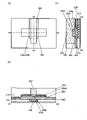
図2に示す表示装置700は、液晶素子775を有する。液晶素子775は、導電層772、導電層774、及びこれらの間に液晶層776を有する。導電層774は、第2の基板705側に設けられ、共通電極としての機能を有する。また、導電層772は、トランジスタ750が有するソース電極またはドレイン電極と電気的に接続される。導電層772は、絶縁体363上に形成され、画素電極として機能する。
図3に示す表示装置700は、発光素子782を有する。発光素子782は、導電層772、EL層786、及び導電膜788を有する。EL層786は、有機化合物、または量子ドットなどの無機化合物を有する。
また、図2及び図3に示す表示装置700に入力装置を設けてもよい。当該入力装置としては、例えば、タッチセンサ等が挙げられる。
図2及び図3に示した表示装置700と異なる構成について、図4及び図5を用いて説明する。なお、図4及び図5は、それぞれ図1に示す一点鎖線Q-Rにおける断面図である。図4は、表示素子として液晶素子を用いた構成であり、図5は、発光素子を用いた構成である。
先の実施の形態で示した表示装置と、異なる構成の例について説明する。以下では、先の実施の形態と重複する部分は説明を省略する場合がある。また、以下で示す図面において、先の実施の形態と同様の機能を有する部分についてはハッチングパターンを同じくし、符号を付さない場合もある。
表示素子として液晶素子を用いる構成について、図6及び図7を用いて説明する。図6に示す表示装置700において、画素部702はトランジスタ750及び容量素子790を有する。ソースドライバ回路部704はトランジスタ441を有する。図6に示す表示装置700は、画素部702が有するトランジスタと、ソースドライバ回路部704が有するトランジスタが、異なる層に形成されている点で、図2に示した表示装置と異なる。図6では、トランジスタ750、およびトランジスタ441のチャネル長方向の断面を示している。トランジスタ750及び容量素子790は、先の記載を参照できるため、詳細な説明は省略する。
表示素子として発光素子を用いる構成について、図8及び図9を用いて説明する。図8に示す表示装置において、画素部702はトランジスタ421、トランジスタ754及び容量素子790を有する。ソースドライバ回路部704はトランジスタ441を有する。図8に示す表示装置は、画素部702が有するトランジスタと、ソースドライバ回路部704が有するトランジスタが、異なる層に形成されている点で、図3に示した表示装置と異なる。図8では、トランジスタ421、トランジスタ754、およびトランジスタ441のチャネル長方向の断面を示している。トランジスタ441、トランジスタ754及び容量素子790は、先の記載を参照できるため、詳細な説明は省略する。
本実施の形態では、本発明の一態様である表示装置に用いることができるトランジスタ及びその作製方法について説明する。
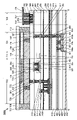
図10(A)、図10(B)、および図10(C)は、本発明の一態様である表示装置に用いることができるトランジスタ200、およびトランジスタ200周辺の上面図および断面図である。画素部702、ソースドライバ回路部704及びゲートドライバ回路部706が有するトランジスタに、トランジスタ200を適用することができる。
図10に示すように、トランジスタ200は、基板(図示しない。)の上に配置された酸化物230aと、酸化物230aの上に配置された酸化物230bと、酸化物230bの上に、互いに離隔して配置された導電体242a、および導電体242bと、導電体242aおよび導電体242b上に配置され、導電体242aと導電体242bの間に重畳して開口が形成された絶縁体280と、開口の中に配置された導電体260と、酸化物230b、導電体242a、導電体242b、および絶縁体280と、導電体260と、の間に配置された絶縁体250と、酸化物230b、導電体242a、導電体242b、および絶縁体280と、絶縁体250と、の間に配置された酸化物230cと、を有する。ここで、図10(B)及び図10(C)に示すように、導電体260の上面は、絶縁体250、絶縁体254、絶縁体244、酸化物230c、および絶縁体280の上面と略一致することが好ましい。なお、以下において、酸化物230a、酸化物230b、および酸化物230cをまとめて酸化物230という場合がある。また、導電体242aおよび導電体242bをまとめて導電体242という場合がある。
トランジスタに用いることができる構成材料について説明する。
絶縁体としては、絶縁性を有する酸化物、窒化物、酸化窒化物、窒化酸化物、金属酸化物、金属酸化窒化物、金属窒化酸化物などがある。
導電体としては、アルミニウム、クロム、銅、銀、金、白金、タンタル、ニッケル、チタン、モリブデン、タングステン、ハフニウム、バナジウム、ニオブ、マンガン、マグネシウム、ジルコニウム、ベリリウム、インジウム、ルテニウム、イリジウム、ストロンチウム、ランタンなどから選ばれた金属元素、または上述した金属元素を成分とする合金か、上述した金属元素を組み合わせた合金等を用いることが好ましい。例えば、窒化タンタル、窒化チタン、タングステン、チタンとアルミニウムを含む窒化物、タンタルとアルミニウムを含む窒化物、酸化ルテニウム、窒化ルテニウム、ストロンチウムとルテニウムを含む酸化物、ランタンとニッケルを含む酸化物などを用いることが好ましい。また、窒化タンタル、窒化チタン、チタンとアルミニウムを含む窒化物、タンタルとアルミニウムを含む窒化物、酸化ルテニウム、窒化ルテニウム、ストロンチウムとルテニウムを含む酸化物、ランタンとニッケルを含む酸化物は、酸化しにくい導電性材料、または、酸素を吸収しても導電性を維持する材料であるため、好ましい。また、リン等の不純物元素を含有させた多結晶シリコンに代表される、電気伝導度が高い半導体、ニッケルシリサイドなどのシリサイドを用いてもよい。
酸化物230として、酸化物半導体として機能する金属酸化物(以下、酸化物半導体ともいう)を用いることが好ましい。以下では、本発明に係る酸化物230に適用可能な金属酸化物について説明する。
以下では、本発明の一態様で開示されるトランジスタに用いることができるCAC(Cloud-Aligned Composite)-OSの構成について説明する。
酸化物半導体は、単結晶酸化物半導体と、それ以外の非単結晶酸化物半導体と、に分けられる。非単結晶酸化物半導体としては、例えば、CAAC-OS(c-axis aligned crystalline oxide semiconductor)、多結晶酸化物半導体、nc-OS(nanocrystalline oxide semiconductor)、擬似非晶質酸化物半導体(a-like OS:amorphous-like oxide semiconductor)および非晶質酸化物半導体などがある。
続いて、上記酸化物半導体をトランジスタに用いる場合について説明する。
ここで、酸化物半導体中における各不純物の影響について説明する。
ここでは、金属酸化物に含まれる、弱いZn-O結合について説明し、該結合を構成する酸素原子および亜鉛原子を低減する方法の一例について示す。
次に、本発明の一態様である表示装置に用いることができるトランジスタ200について、作製方法を図11乃至図16を用いて説明する。また、図11乃至図16において、各図の(A)は上面図を示す。また、各図の(B)は、(A)に示すA1-A2の一点鎖線で示す部位に対応する断面図であり、トランジスタ200のチャネル長方向の断面図でもある。また、各図の(C)は、(A)にA3-A4の一点鎖線で示す部位に対応する断面図であり、トランジスタ200のチャネル幅方向の断面図でもある。なお、各図の(A)の上面図では、図の明瞭化のために一部の要素を省いて図示している。
あるいは、該絶縁膜の成膜温度と同じ温度で行うことが好ましい。ここで、成膜温度とは、成膜中の基板温度に限らず、成膜装置の設定温度の場合を含む。例えば、該絶縁膜を250℃で成膜する場合、当該加熱処理の温度は250℃とすることが好ましい。当該加熱処理は、減圧下で行うことが好ましく、例えば、真空雰囲気で行ってもよい。真空雰囲気は、ターボ分子ポンプ等で排気を行うことで維持される。真空雰囲気では、処理室の圧力は、1×10⁻²Pa以下、好ましくは1×10⁻³Pa以下とすればよい。
図17(A)、図17(B)、および図17(C)は、本発明の一態様である表示装置に用いることができるトランジスタ200A、およびトランジスタ200A周辺の上面図および断面図である。画素部702、ソースドライバ回路部704及びゲートドライバ回路部706が有するトランジスタに、トランジスタ200Aを適用することができる。また、トランジスタ200Aについて、作製方法を図18に示す。また、図17及び図18において、各図の(A)は上面図を示す。また、各図の(B)は、図17(A)に示すA1-A2の一点鎖線で示す部位に対応する断面図であり、トランジスタ200Aのチャネル長方向の断面図でもある。また、各図の(C)は、図17(A)にA3-A4の一点鎖線で示す部位に対応する断面図であり、トランジスタ200Aのチャネル幅方向の断面図でもある。各図の(A)の上面図では、図の明瞭化のために一部の要素を省いて図示している。
図19(A)、図19(B)、および図19(C)は、本発明の一態様である表示装置に用いることができるトランジスタ200B、およびトランジスタ200B周辺の上面図および断面図である。画素部702、ソースドライバ回路部704及びゲートドライバ回路部706が有するトランジスタに、トランジスタ200Bを適用することができる。また、トランジスタ200Bについて、作製方法を図20乃至図24に示す。また、図19乃至図24において、各図の(A)は上面図を示す。また、各図の(B)は、図19(A)に示すA1-A2の一点鎖線で示す部位に対応する断面図であり、トランジスタ200Bのチャネル長方向の断面図でもある。また、各図の(C)は、図19(A)にA3-A4の一点鎖線で示す部位に対応する断面図であり、トランジスタ200Bのチャネル幅方向の断面図でもある。各図の(A)の上面図では、図の明瞭化のために一部の要素を省いて図示している。
図25(A)、図25(B)、および図25(C)は、本発明の一態様である表示装置に用いることができるトランジスタ200C、およびトランジスタ200C周辺の上面図および断面図である。画素部702、ソースドライバ回路部704及びゲートドライバ回路部706が有するトランジスタに、トランジスタ200Cを適用することができる。また、トランジスタ200Cについて、作製方法を図26及び図27に示す。また、図25乃至図27において、各図の(A)は上面図を示す。また、各図の(B)は、図25(A)に示すA1-A2の一点鎖線で示す部位に対応する断面図であり、トランジスタ200Cのチャネル長方向の断面図でもある。また、各図の(C)は、図25(A)にA3-A4の一点鎖線で示す部位に対応する断面図であり、トランジスタ200Cのチャネル幅方向の断面図でもある。各図の(A)の上面図では、図の明瞭化のために一部の要素を省いて図示している。
図28(A)、図28(B)および図28(C)は、本発明の一態様である表示装置に用いることができるトランジスタ200D、およびトランジスタ200D周辺の上面図および断面図である。画素部702、ソースドライバ回路部704及びゲートドライバ回路部706が有するトランジスタに、トランジスタ200Dを適用することができる。
次に、図28に示す、本発明の一態様に係るトランジスタ200Dについて、作製方法を図30乃至図38を用いて説明する。また、図30乃至図38において、各図の(A)は上面図を示す。また、各図の(B)は、(A)にA1-A2の一点鎖線で示す部位に対応する断面図であり、トランジスタ200Dのチャネル長方向の断面図でもある。また、各図の(C)は、(A)にA3-A4の一点鎖線で示す部位に対応する断面図であり、トランジスタ200Dのチャネル幅方向の断面図でもある。なお、各図の(A)の上面図では、図の明瞭化のために一部の要素を省いて図示している。また、<トランジスタの作製方法1>に示すトランジスタ200と同符号を付記した構成要素は、<トランジスタの作製方法1>を参酌することができる。
図39(A)、図39(B)、および図39(C)は、本発明の一態様である表示装置に用いることができるトランジスタ200E、およびトランジスタ200E周辺の上面図および断面図である。画素部702、ソースドライバ回路部704及びゲートドライバ回路部706が有するトランジスタに、トランジスタ200Eを適用することができる。図39(A)は、トランジスタ200Eの上面図である。図39(B)は、図39(A)にA1-A2の一点鎖線で示す部位の断面図であり、トランジスタ200Eのチャネル長方向の断面図でもある。また、図39(C)は、図39(A)にA3-A4の一点鎖線で示す部位の断面図であり、トランジスタ200Eのチャネル幅方向の断面図でもある。なお、図39(A)の上面図では、図の明瞭化のために一部の要素を省いて図示している。また、図40は、図39(B)における酸化物230bおよびその近傍の拡大図である。
図48(A)、図48(B)、および図48(C)は、本発明の一態様である表示装置に用いることができるトランジスタ200F、およびトランジスタ200F周辺の上面図および断面図である。画素部702、ソースドライバ回路部704及びゲートドライバ回路部706が有するトランジスタに、トランジスタ200Fを適用することができる。図48(A)は、トランジスタ200Fの上面図である。また、図48(B)は、図48(A)に示すA1-A2の一点鎖線で示す部位の断面図であり、トランジスタ200Fのチャネル長方向の断面図でもある。また、図48(C)は、図48(A)にA3-A4の一点鎖線で示す部位の断面図であり、トランジスタ200Fのチャネル幅方向の断面図でもある。なお、図48(A)の上面図では、図の明瞭化のために一部の要素を省いて図示している。また、図49は、図48(B)における酸化物230bおよびその近傍の拡大図である。
本実施の形態では、本発明の一態様である表示装置について、説明する。
画素に表示される階調を補正するためのメモリを備える画素回路と、これを有する表示装置について説明する。先の実施の形態で例示したトランジスタは、以下で例示する画素回路に用いられるトランジスタに適用することができる。
図52(A)に、画素回路400の回路図を示す。画素回路400は、トランジスタM1、トランジスタM2、容量C1、及び回路401を有する。また画素回路400には、配線S1、配線S2、配線G1、及び配線G2が接続される。
続いて、図52(B)を用いて、画素回路400の動作方法の一例を説明する。図52(B)は、画素回路400の動作に係るタイミングチャートである。なおここでは説明を容易にするため、配線抵抗などの各種抵抗や、トランジスタや配線などの寄生容量、及びトランジスタのしきい値電圧などの影響は考慮しない。
期間T1では、配線G1と配線G2の両方に、トランジスタをオン状態にする電位を与える。また、配線S1には固定電位である電位Vrefを供給し、配線S2には第1データ電位Vwを供給する。
続いて期間T2では、配線G1にはトランジスタM1をオン状態とする電位を与え、配線G2にはトランジスタM2をオフ状態とする電位を与える。また、配線S1には第2データ電位Vdataを供給する。配線S2には所定の定電位を与える、またはフローティングとしてもよい。
〔液晶素子を用いた例〕
図52(C)に示す画素回路400LCは、回路401LCを有する。回路401LCは、液晶素子LCと、容量C2とを有する。
図52(D)に示す画素回路400ELは、回路401ELを有する。回路401ELは、発光素子EL、トランジスタM3、及び容量C2を有する。
本実施の形態では、本発明の一態様である表示装置に用いることができる発光素子について説明する。
図53(A)には、一対の電極間にEL層を挟んでなる発光素子を示す。具体的には、第1の電極1101と第2の電極1102との間に発光層を含むEL層1103が挟まれた構造を有する。
次に、発光素子の具体的な構造および作製方法について説明する。なお、図53(A)乃至図53(D)において、符号が共通である場合は説明も共通とする。
第1の電極1101および第2の電極1102を形成する材料としては、上述した素子構造における両電極の機能が満たせるのであれば、以下に示す材料を適宜組み合わせて用いることができる。例えば、金属、合金、電気伝導性化合物、およびこれらの混合物などを適宜用いることができる。
正孔注入層(1111、1111a、1111b)は、陽極である第1の電極1101や電荷発生層(1104)からEL層(1103、1103a、1103b)に正孔(ホール)を注入する層であり、正孔注入性の高い材料を含む層である。
発光層(1113、1113a、1113b)は、発光物質を含む層である。なお、発光物質としては、青色、紫色、青紫色、緑色、黄緑色、黄色、橙色、赤色などの発光色を呈する物質を適宜用いる。また、複数の発光層(1113a、1113b)に異なる発光物質を用いることにより異なる発光色を呈する構成(例えば、補色の関係にある発光色を組み合わせて得られる白色発光)とすることができる。さらに、一つの発光層が異なる発光物質を有する積層構造であってもよい。
電子輸送層(1114、1114a、1114b)は、電子注入層(1115、1115a、1115b)によって、第2の電極1102から注入された電子を発光層(1113、1113a、1113b)に輸送する層である。なお、電子輸送層(1114、1114a、1114b)は、電子輸送性材料を含む層である。電子輸送層(1114、1114a、1114b)に用いる電子輸送性材料は、1×10⁻⁶cm2/Vs以上の電子移動度を有する物質が好ましい。なお、正孔よりも電子の輸送性の高い物質であれば、これら以外のものを用いることができる。
電子注入層(1115、1115a、1115b)は、電子注入性の高い物質を含む層である。電子注入層(1115、1115a、1115b)には、フッ化リチウム(LiF)、フッ化セシウム(CsF)、フッ化カルシウム(CaF2)、リチウム酸化物(LiOx)等のようなアルカリ金属、アルカリ土類金属、またはそれらの化合物を用いることができる。また、フッ化エルビウム(ErF3)のような希土類金属化合物を用いることができる。また、電子注入層(1115、1115a、1115b)にエレクトライドを用いてもよい。エレクトライドとしては、例えば、カルシウムとアルミニウムの混合酸化物に電子を高濃度添加した物質等が挙げられる。なお、上述した電子輸送層(1114、1114a、1114b)を構成する物質を用いることもできる。
図53(D)に示す発光素子において、電荷発生層1104は、第1の電極(陽極)1101と第2の電極(陰極)1102との間に電圧を印加したときに、EL層1103aに電子を注入し、EL層1103bに正孔を注入する機能を有する。なお、電荷発生層1104は、正孔輸送性材料に電子受容体(アクセプター)が添加された構成であっても、電子輸送性材料に電子供与体(ドナー)が添加された構成であってもよい。また、これらの両方の構成が積層されていてもよい。なお、上述した材料を用いて電荷発生層1104を形成することにより、EL層が積層された場合における駆動電圧の上昇を抑制することができる。
本実施の形態では、本発明の一態様である表示装置を備える電子機器について説明する。
本実施の形態では、本発明の一態様である表示装置を備える電子機器について説明する。
Claims (14)
- 第1のトランジスタと、前記第1のトランジスタと電気的に接続される表示素子と、を有し、
前記第1のトランジスタは、第1の酸化物と、第2の酸化物と、導電体と、第1の絶縁体と、第2の絶縁体と、第3の絶縁体と、第4の絶縁体と、を有し、
前記第2の酸化物は、前記第1の酸化物上に位置し、
前記第1の絶縁体は、前記第2の酸化物上に位置し、
前記導電体は、前記第1の絶縁体上に位置し、
前記第2の絶縁体は、前記第1の酸化物の上面の一部、前記第1の酸化物の側面の一部、及び前記第2の酸化物の側面の一部と接し、
前記第3の絶縁体は、前記第2の絶縁体上に位置し、
前記第2の酸化物の一部、及び前記第1の絶縁体の一部は、前記導電体の側面と、前記第3の絶縁体の側面との間に位置し、
前記第4の絶縁体は、前記第2の酸化物の上面、前記第1の絶縁体の上面、前記導電体の上面、及び前記第3の絶縁体の上面と接し、
前記第1の酸化物は、第1の領域と、第2の領域と、前記第1の領域と前記第2の領域との間に位置する第3の領域と、前記第1の領域と前記第3の領域との間に位置する第4の領域と、前記第2の領域と前記第3の領域との間に位置する第5の領域と、を有し、
前記導電体は、前記第3の領域と重畳するように、前記第3の領域の上方に位置し、
前記第2の絶縁体は、前記第1の領域、および前記第2の領域と接し、
前記第1の領域、及び前記第2の領域の抵抗は、前記第3の領域の抵抗より低く、
前記第4の領域、及び前記第5の領域の抵抗は、前記第3の領域の抵抗より低く、かつ前記第1の領域、及び前記第2の領域の抵抗より高い表示装置。 - 第1のトランジスタと、前記第1のトランジスタと電気的に接続される表示素子と、構造体と、を有し、
前記第1のトランジスタは、第1の酸化物と、第2の酸化物と、導電体と、第1の絶縁体と、第2の絶縁体と、第3の絶縁体と、第4の絶縁体と、を有し、
前記第2の酸化物は、前記第1の酸化物上に位置し、
前記第1の絶縁体は、前記第2の酸化物上に位置し、
前記導電体は、前記第1の絶縁体上に位置し、
前記第2の絶縁体は、前記第1の酸化物の上面の一部、前記第1の酸化物の側面の一部、及び前記第2の酸化物の側面の一部と接し、
前記第3の絶縁体は、前記第2の絶縁体上に位置し、
前記第2の酸化物の一部、及び前記第1の絶縁体の一部は、前記導電体の側面と、前記第3の絶縁体の側面との間に位置し、
前記第4の絶縁体は、前記第2の酸化物の上面、前記第1の絶縁体の上面、前記導電体の上面、及び前記第3の絶縁体の上面と接し、
前記第1の酸化物は、第1の領域と、第2の領域と、前記第1の領域と前記第2の領域との間に位置する第3の領域と、前記第1の領域と前記第3の領域との間に位置する第4の領域と、前記第2の領域と前記第3の領域との間に位置する第5の領域と、を有し、
前記導電体は、前記第3の領域と重畳するように、前記第3の領域の上方に位置し、
前記第2の絶縁体は、前記第1の領域、および前記第2の領域と接し、
前記第1の領域、及び前記第2の領域の抵抗は、前記第3の領域の抵抗より低く、
前記第4の領域、及び前記第5の領域の抵抗は、前記第3の領域の抵抗より低く、かつ前記第1の領域、及び前記第2の領域の抵抗より高く、
前記構造体は、前記表示素子を有する層と同じ層に配置され、
前記構造体は、前記第1のトランジスタと重なる領域を有する表示装置。 - 第1のトランジスタと、第2のトランジスタと、前記第2のトランジスタと電気的に接続される表示素子と、を有し、
前記第1のトランジスタは、第1の酸化物と、第2の酸化物と、導電体と、第1の絶縁体と、第2の絶縁体と、第3の絶縁体と、第4の絶縁体と、を有し、
前記第2の酸化物は、前記第1の酸化物上に位置し、
前記第1の絶縁体は、前記第2の酸化物上に位置し、
前記導電体は、前記第1の絶縁体上に位置し、
前記第2の絶縁体は、前記第1の酸化物の上面の一部、前記第1の酸化物の側面の一部、及び前記第2の酸化物の側面の一部と接し、
前記第3の絶縁体は、前記第2の絶縁体上に位置し、
前記第2の酸化物の一部、及び前記第1の絶縁体の一部は、前記導電体の側面と、前記第3の絶縁体の側面との間に位置し、
前記第4の絶縁体は、前記第2の酸化物の上面、前記第1の絶縁体の上面、前記導電体の上面、及び前記第3の絶縁体の上面と接し、
前記第1の酸化物は、第1の領域と、第2の領域と、前記第1の領域と前記第2の領域との間に位置する第3の領域と、前記第1の領域と前記第3の領域との間に位置する第4の領域と、前記第2の領域と前記第3の領域との間に位置する第5の領域と、を有し、
前記導電体は、前記第3の領域と重畳するように、前記第3の領域の上方に位置し、
前記第2の絶縁体は、前記第1の領域、および前記第2の領域と接し、
前記第1の領域、及び前記第2の領域の抵抗は、前記第3の領域の抵抗より低く、
前記第4の領域、及び前記第5の領域の抵抗は、前記第3の領域の抵抗より低く、かつ前記第1の領域、及び前記第2の領域の抵抗より高く、
前記第1のトランジスタを有する層は、前記表示素子を有する層と、前記第2のトランジスタが有する層との間に位置する表示装置。 - 第1のトランジスタと、第2のトランジスタと、前記第2のトランジスタと電気的に接続される表示素子と、遮光膜と、を有し、
前記第1のトランジスタは、第1の酸化物と、第2の酸化物と、導電体と、第1の絶縁体と、第2の絶縁体と、第3の絶縁体と、第4の絶縁体と、を有し、
前記第2の酸化物は、前記第1の酸化物上に位置し、
前記第1の絶縁体は、前記第2の酸化物上に位置し、
前記導電体は、前記第1の絶縁体上に位置し、
前記第2の絶縁体は、前記第1の酸化物の上面の一部、前記第1の酸化物の側面の一部、及び前記第2の酸化物の側面の一部と接し、
前記第3の絶縁体は、前記第2の絶縁体上に位置し、
前記第2の酸化物の一部、及び前記第1の絶縁体の一部は、前記導電体の側面と、前記第3の絶縁体の側面との間に位置し、
前記第4の絶縁体は、前記第2の酸化物の上面、前記第1の絶縁体の上面、前記導電体の上面、及び前記第3の絶縁体の上面と接し、
前記第1の酸化物は、第1の領域と、第2の領域と、前記第1の領域と前記第2の領域との間に位置する第3の領域と、前記第1の領域と前記第3の領域との間に位置する第4の領域と、前記第2の領域と前記第3の領域との間に位置する第5の領域と、を有し、
前記導電体は、前記第3の領域と重畳するように、前記第3の領域の上方に位置し、
前記第2の絶縁体は、前記第1の領域、および前記第2の領域と接し、
前記第1の領域、及び前記第2の領域の抵抗は、前記第3の領域の抵抗より低く、
前記第4の領域、及び前記第5の領域の抵抗は、前記第3の領域の抵抗より低く、かつ前記第1の領域、及び前記第2の領域の抵抗より高く、
前記遮光膜は、前記表示素子の上方に位置し、
前記遮光膜、前記第1のトランジスタ及び前記第2のトランジスタは、重なる領域を有する表示装置。 - 請求項3又は請求項4において、
前記第2のトランジスタは、チャネル形成領域にシリコンを有し、かつnチャネル型である表示装置。 - 請求項3又は請求項4において、
前記第2のトランジスタは、チャネル形成領域にシリコンを有し、かつpチャネル型である表示装置。 - 請求項1乃至請求項6のいずれか一において、
前記第1の領域、および前記第2の領域は、リン、およびホウ素のいずれか一以上を有する表示装置。 - 請求項1乃至請求項7のいずれか一において、
前記第2の酸化物は、前記第1の領域の一部、および前記第2の領域の一部と重畳する表示装置。 - 請求項1乃至請求項8のいずれか一において、
さらに、第5の絶縁体を有し、
前記第5の絶縁体は、前記第2の絶縁体の上面、および前記第2の酸化物の側面の一部と接する表示装置。 - 請求項9において、
前記第4の領域、および前記第5の領域は、リン、およびホウ素のいずれか一以上を有する表示装置。 - 請求項9又は請求項10において、
前記第1の領域および前記第2の領域は、前記第4の領域および前記第5の領域よりも、リン、またはホウ素を多く有する表示装置。 - 請求項9乃至請求項11のいずれか一において、
前記第2の酸化物は、前記第4の領域の一部、および前記第5の領域の一部と重畳する表示装置。 - 請求項1乃至請求項12のいずれか一において、
前記表示素子は、液晶素子である表示装置。 - 請求項1乃至請求項12のいずれか一において、
前記表示素子は、発光素子である表示装置。
Priority Applications (1)
| Application Number | Priority Date | Filing Date | Title |
|---|---|---|---|
| JP2022190081A JP2023024481A (ja) | 2018-02-08 | 2022-11-29 | 表示装置 |
Applications Claiming Priority (5)
| Application Number | Priority Date | Filing Date | Title |
|---|---|---|---|
| JP2018021216 | 2018-02-08 | ||
| JP2018021216 | 2018-02-08 | ||
| JP2018025658 | 2018-02-16 | ||
| JP2018025658 | 2018-02-16 | ||
| PCT/IB2019/050660 WO2019155318A1 (ja) | 2018-02-08 | 2019-01-28 | 表示装置 |
Related Child Applications (1)
| Application Number | Title | Priority Date | Filing Date |
|---|---|---|---|
| JP2022190081A Division JP2023024481A (ja) | 2018-02-08 | 2022-11-29 | 表示装置 |
Publications (3)
| Publication Number | Publication Date |
|---|---|
| JPWO2019155318A1 JPWO2019155318A1 (ja) | 2021-02-25 |
| JPWO2019155318A5 JPWO2019155318A5 (ja) | 2022-01-19 |
| JP7186732B2 true JP7186732B2 (ja) | 2022-12-09 |
Family
ID=67548979
Family Applications (2)
| Application Number | Title | Priority Date | Filing Date |
|---|---|---|---|
| JP2019571122A Active JP7186732B2 (ja) | 2018-02-08 | 2019-01-28 | 表示装置 |
| JP2022190081A Pending JP2023024481A (ja) | 2018-02-08 | 2022-11-29 | 表示装置 |
Family Applications After (1)
| Application Number | Title | Priority Date | Filing Date |
|---|---|---|---|
| JP2022190081A Pending JP2023024481A (ja) | 2018-02-08 | 2022-11-29 | 表示装置 |
Country Status (5)
| Country | Link |
|---|---|
| US (1) | US11417687B2 (ja) |
| JP (2) | JP7186732B2 (ja) |
| KR (2) | KR102579601B1 (ja) |
| TW (1) | TWI814776B (ja) |
| WO (1) | WO2019155318A1 (ja) |
Families Citing this family (3)
| Publication number | Priority date | Publication date | Assignee | Title |
|---|---|---|---|---|
| KR20210130724A (ko) | 2019-02-22 | 2021-11-01 | 가부시키가이샤 한도오따이 에네루기 켄큐쇼 | 안경형 전자 기기 |
| JP6967627B2 (ja) * | 2020-05-08 | 2021-11-17 | アオイ電子株式会社 | 半導体装置 |
| IL304070A (en) * | 2020-12-30 | 2023-08-01 | Asml Netherlands Bv | Apparatus and method for cleaning a test system |
Citations (8)
| Publication number | Priority date | Publication date | Assignee | Title |
|---|---|---|---|---|
| JP2013145878A (ja) | 2011-12-14 | 2013-07-25 | Semiconductor Energy Lab Co Ltd | 半導体装置、及び当該半導体装置を用いた表示装置 |
| WO2014112279A1 (ja) | 2013-01-16 | 2014-07-24 | ソニー株式会社 | 固体撮像素子および電子機器 |
| JP2016157937A (ja) | 2015-02-24 | 2016-09-01 | 株式会社半導体エネルギー研究所 | 半導体装置およびその作製方法 |
| JP2016167584A (ja) | 2015-03-03 | 2016-09-15 | 株式会社半導体エネルギー研究所 | 半導体装置およびその作製方法 |
| WO2017009738A1 (ja) | 2015-07-14 | 2017-01-19 | 株式会社半導体エネルギー研究所 | 半導体装置およびその作製方法 |
| WO2017103723A1 (ja) | 2015-12-15 | 2017-06-22 | 株式会社半導体エネルギー研究所 | トランジスタ、半導体装置、電子機器およびトランジスタの作製方法 |
| JP2017147445A (ja) | 2016-02-17 | 2017-08-24 | 株式会社半導体エネルギー研究所 | 半導体装置、電子機器 |
| WO2017144994A1 (ja) | 2016-02-22 | 2017-08-31 | 株式会社半導体エネルギー研究所 | トランジスタおよびその作製方法、半導体ウエハならびに電子機器 |
Family Cites Families (13)
| Publication number | Priority date | Publication date | Assignee | Title |
|---|---|---|---|---|
| EP0278619B1 (en) * | 1987-01-30 | 1993-12-08 | Texas Instruments Incorporated | Integrated bipolar and CMOS transistor fabrication process |
| JP3931138B2 (ja) * | 2002-12-25 | 2007-06-13 | 三菱電機株式会社 | 電力用半導体装置及び電力用半導体装置の製造方法 |
| KR102071545B1 (ko) | 2012-05-31 | 2020-01-30 | 가부시키가이샤 한도오따이 에네루기 켄큐쇼 | 반도체 장치 |
| US9449853B2 (en) * | 2013-09-04 | 2016-09-20 | Semiconductor Energy Laboratory Co., Ltd. | Method for manufacturing semiconductor device comprising electron trap layer |
| JP6823927B2 (ja) | 2015-01-21 | 2021-02-03 | 株式会社半導体エネルギー研究所 | 表示システム |
| US10553690B2 (en) * | 2015-08-04 | 2020-02-04 | Semiconductor Energy Laboratory Co., Ltd. | Semiconductor device and manufacturing method thereof |
| JP6850096B2 (ja) | 2015-09-24 | 2021-03-31 | 株式会社半導体エネルギー研究所 | 半導体装置の作製方法及び電子機器の作製方法 |
| KR102458660B1 (ko) | 2016-08-03 | 2022-10-26 | 가부시키가이샤 한도오따이 에네루기 켄큐쇼 | 표시 장치 및 전자 기기 |
| US10528079B2 (en) | 2016-08-26 | 2020-01-07 | Semiconductor Energy Laboratory Co., Ltd. | Data processing device, display method, input/output method, server system, and computer program |
| JP2018049267A (ja) | 2016-09-16 | 2018-03-29 | 株式会社半導体エネルギー研究所 | 表示システム、電子機器および表示方法 |
| WO2018087625A1 (en) | 2016-11-10 | 2018-05-17 | Semiconductor Energy Laboratory Co., Ltd. | Display device and driving method of display device |
| US10330993B2 (en) | 2016-12-23 | 2019-06-25 | Semiconductor Energy Laboratory Co., Ltd. | Display device |
| WO2018197987A1 (en) | 2017-04-28 | 2018-11-01 | Semiconductor Energy Laboratory Co., Ltd. | Imaging display device and electronic device |
-
2019
- 2019-01-28 JP JP2019571122A patent/JP7186732B2/ja active Active
- 2019-01-28 WO PCT/IB2019/050660 patent/WO2019155318A1/ja active Application Filing
- 2019-01-28 KR KR1020207023783A patent/KR102579601B1/ko active IP Right Grant
- 2019-01-28 KR KR1020237031194A patent/KR20230133949A/ko active IP Right Grant
- 2019-01-28 US US16/965,053 patent/US11417687B2/en active Active
- 2019-01-31 TW TW108103699A patent/TWI814776B/zh active
-
2022
- 2022-11-29 JP JP2022190081A patent/JP2023024481A/ja active Pending
Patent Citations (8)
| Publication number | Priority date | Publication date | Assignee | Title |
|---|---|---|---|---|
| JP2013145878A (ja) | 2011-12-14 | 2013-07-25 | Semiconductor Energy Lab Co Ltd | 半導体装置、及び当該半導体装置を用いた表示装置 |
| WO2014112279A1 (ja) | 2013-01-16 | 2014-07-24 | ソニー株式会社 | 固体撮像素子および電子機器 |
| JP2016157937A (ja) | 2015-02-24 | 2016-09-01 | 株式会社半導体エネルギー研究所 | 半導体装置およびその作製方法 |
| JP2016167584A (ja) | 2015-03-03 | 2016-09-15 | 株式会社半導体エネルギー研究所 | 半導体装置およびその作製方法 |
| WO2017009738A1 (ja) | 2015-07-14 | 2017-01-19 | 株式会社半導体エネルギー研究所 | 半導体装置およびその作製方法 |
| WO2017103723A1 (ja) | 2015-12-15 | 2017-06-22 | 株式会社半導体エネルギー研究所 | トランジスタ、半導体装置、電子機器およびトランジスタの作製方法 |
| JP2017147445A (ja) | 2016-02-17 | 2017-08-24 | 株式会社半導体エネルギー研究所 | 半導体装置、電子機器 |
| WO2017144994A1 (ja) | 2016-02-22 | 2017-08-31 | 株式会社半導体エネルギー研究所 | トランジスタおよびその作製方法、半導体ウエハならびに電子機器 |
Also Published As
| Publication number | Publication date |
|---|---|
| KR20230133949A (ko) | 2023-09-19 |
| JPWO2019155318A1 (ja) | 2021-02-25 |
| JP2023024481A (ja) | 2023-02-16 |
| KR102579601B1 (ko) | 2023-09-15 |
| KR20200115539A (ko) | 2020-10-07 |
| WO2019155318A1 (ja) | 2019-08-15 |
| TW201937254A (zh) | 2019-09-16 |
| US11417687B2 (en) | 2022-08-16 |
| US20210111196A1 (en) | 2021-04-15 |
| TWI814776B (zh) | 2023-09-11 |
Similar Documents
| Publication | Publication Date | Title |
|---|---|---|
| JP2023024481A (ja) | 表示装置 | |
| WO2021130585A1 (ja) | 表示装置、および電子機器 | |
| TW202343590A (zh) | 半導體裝置 | |
| US20220285560A1 (en) | Transistor and display device | |
| WO2022118151A1 (ja) | 表示システム、及び電子機器 | |
| TW202409679A (zh) | 顯示裝置 | |
| WO2023100013A1 (ja) | 半導体装置、半導体装置の作製方法 | |
| WO2022162501A1 (ja) | 表示装置 | |
| US20220320184A1 (en) | Display apparatus, display module, electronic device, and method for manufacturing display apparatus | |
| WO2022224091A1 (ja) | 表示装置 | |
| WO2022214904A1 (ja) | 表示装置 | |
| WO2022153138A1 (ja) | 表示装置、表示装置の作製方法、及び電子機器 | |
| WO2024033742A1 (ja) | シフトレジスタ | |
| WO2022224073A1 (ja) | 表示装置、及び表示装置の作製方法 | |
| WO2022248962A1 (ja) | 表示装置、表示モジュール、及び、電子機器 | |
| US20240054955A1 (en) | Display device | |
| WO2022162496A1 (ja) | 表示装置の作製方法、表示装置、表示モジュール、及び、電子機器 | |
| WO2022200916A1 (ja) | 表示装置、表示装置の作製方法、表示モジュール、及び電子機器 | |
| WO2022208231A1 (ja) | 表示装置 | |
| KR20230156066A (ko) | 표시 장치 | |
| CN114902323A (zh) | 显示装置及电子设备 | |
| KR20230166098A (ko) | 표시 장치, 표시 장치의 제작 방법, 표시 모듈, 전자 기기 | |
| KR20230131471A (ko) | 표시 장치의 제작 방법 | |
| TW202232796A (zh) | 顯示裝置 | |
| CN116745836A (zh) | 显示装置及电子设备 |
Legal Events
| Date | Code | Title | Description |
|---|---|---|---|
| A521 | Request for written amendment filed |
Free format text: JAPANESE INTERMEDIATE CODE: A523 Effective date: 20220111 |
|
| A621 | Written request for application examination |
Free format text: JAPANESE INTERMEDIATE CODE: A621 Effective date: 20220111 |
|
| TRDD | Decision of grant or rejection written | ||
| A01 | Written decision to grant a patent or to grant a registration (utility model) |
Free format text: JAPANESE INTERMEDIATE CODE: A01 Effective date: 20221108 |
|
| A61 | First payment of annual fees (during grant procedure) |
Free format text: JAPANESE INTERMEDIATE CODE: A61 Effective date: 20221129 |
|
| R150 | Certificate of patent or registration of utility model |
Ref document number: 7186732 Country of ref document: JP Free format text: JAPANESE INTERMEDIATE CODE: R150 |