WO2022162501A1 - 表示装置 - Google Patents
表示装置 Download PDFInfo
- Publication number
- WO2022162501A1 WO2022162501A1 PCT/IB2022/050412 IB2022050412W WO2022162501A1 WO 2022162501 A1 WO2022162501 A1 WO 2022162501A1 IB 2022050412 W IB2022050412 W IB 2022050412W WO 2022162501 A1 WO2022162501 A1 WO 2022162501A1
- Authority
- WO
- WIPO (PCT)
- Prior art keywords
- layer
- light
- film
- display
- display device
- Prior art date
Links
- 230000015572 biosynthetic process Effects 0.000 claims description 41
- 239000010410 layer Substances 0.000 description 811
- 239000010408 film Substances 0.000 description 360
- 238000005401 electroluminescence Methods 0.000 description 240
- 239000004065 semiconductor Substances 0.000 description 123
- 239000000463 material Substances 0.000 description 119
- 239000000758 substrate Substances 0.000 description 110
- 238000000034 method Methods 0.000 description 96
- 230000006870 function Effects 0.000 description 93
- 239000011241 protective layer Substances 0.000 description 60
- 238000005530 etching Methods 0.000 description 53
- 230000001681 protective effect Effects 0.000 description 44
- 239000000126 substance Substances 0.000 description 43
- 239000011701 zinc Substances 0.000 description 43
- 239000013078 crystal Substances 0.000 description 37
- 238000005755 formation reaction Methods 0.000 description 37
- 238000004519 manufacturing process Methods 0.000 description 37
- 229910052751 metal Inorganic materials 0.000 description 34
- 230000003287 optical effect Effects 0.000 description 33
- 239000002184 metal Substances 0.000 description 29
- 238000010586 diagram Methods 0.000 description 27
- 238000002347 injection Methods 0.000 description 27
- 239000007924 injection Substances 0.000 description 27
- 229920005989 resin Polymers 0.000 description 26
- 239000011347 resin Substances 0.000 description 26
- 239000012535 impurity Substances 0.000 description 24
- 229910052760 oxygen Inorganic materials 0.000 description 22
- XUIMIQQOPSSXEZ-UHFFFAOYSA-N Silicon Chemical compound [Si] XUIMIQQOPSSXEZ-UHFFFAOYSA-N 0.000 description 21
- QVGXLLKOCUKJST-UHFFFAOYSA-N atomic oxygen Chemical compound [O] QVGXLLKOCUKJST-UHFFFAOYSA-N 0.000 description 21
- 239000001301 oxygen Substances 0.000 description 21
- 229910052710 silicon Inorganic materials 0.000 description 21
- 239000010703 silicon Substances 0.000 description 21
- XLYOFNOQVPJJNP-UHFFFAOYSA-N water Substances O XLYOFNOQVPJJNP-UHFFFAOYSA-N 0.000 description 20
- 229910044991 metal oxide Inorganic materials 0.000 description 18
- 150000004706 metal oxides Chemical class 0.000 description 18
- XLOMVQKBTHCTTD-UHFFFAOYSA-N Zinc monoxide Chemical compound [Zn]=O XLOMVQKBTHCTTD-UHFFFAOYSA-N 0.000 description 17
- 239000007789 gas Substances 0.000 description 17
- 239000000203 mixture Substances 0.000 description 17
- 125000004429 atom Chemical group 0.000 description 16
- 150000002894 organic compounds Chemical class 0.000 description 16
- IJGRMHOSHXDMSA-UHFFFAOYSA-N Atomic nitrogen Chemical compound N#N IJGRMHOSHXDMSA-UHFFFAOYSA-N 0.000 description 15
- VYPSYNLAJGMNEJ-UHFFFAOYSA-N Silicium dioxide Chemical compound O=[Si]=O VYPSYNLAJGMNEJ-UHFFFAOYSA-N 0.000 description 15
- 238000000231 atomic layer deposition Methods 0.000 description 15
- 239000003990 capacitor Substances 0.000 description 15
- 229910052733 gallium Inorganic materials 0.000 description 15
- 229910052738 indium Inorganic materials 0.000 description 15
- PXHVJJICTQNCMI-UHFFFAOYSA-N Nickel Chemical compound [Ni] PXHVJJICTQNCMI-UHFFFAOYSA-N 0.000 description 14
- 238000001312 dry etching Methods 0.000 description 14
- 239000001257 hydrogen Substances 0.000 description 14
- 229910052739 hydrogen Inorganic materials 0.000 description 14
- GYHNNYVSQQEPJS-UHFFFAOYSA-N Gallium Chemical compound [Ga] GYHNNYVSQQEPJS-UHFFFAOYSA-N 0.000 description 13
- UFHFLCQGNIYNRP-UHFFFAOYSA-N Hydrogen Chemical compound [H][H] UFHFLCQGNIYNRP-UHFFFAOYSA-N 0.000 description 13
- 229910052782 aluminium Inorganic materials 0.000 description 13
- XAGFODPZIPBFFR-UHFFFAOYSA-N aluminium Chemical compound [Al] XAGFODPZIPBFFR-UHFFFAOYSA-N 0.000 description 13
- 230000005525 hole transport Effects 0.000 description 13
- APFVFJFRJDLVQX-UHFFFAOYSA-N indium atom Chemical compound [In] APFVFJFRJDLVQX-UHFFFAOYSA-N 0.000 description 13
- 238000004544 sputter deposition Methods 0.000 description 13
- XEEYBQQBJWHFJM-UHFFFAOYSA-N Iron Chemical compound [Fe] XEEYBQQBJWHFJM-UHFFFAOYSA-N 0.000 description 12
- 239000003086 colorant Substances 0.000 description 12
- 238000012545 processing Methods 0.000 description 12
- -1 aromatic amine compounds Chemical class 0.000 description 11
- 230000004888 barrier function Effects 0.000 description 11
- 210000001508 eye Anatomy 0.000 description 11
- 239000010409 thin film Substances 0.000 description 11
- 230000032258 transport Effects 0.000 description 11
- 229910052581 Si3N4 Inorganic materials 0.000 description 10
- 238000002441 X-ray diffraction Methods 0.000 description 10
- 239000012790 adhesive layer Substances 0.000 description 10
- 238000005229 chemical vapour deposition Methods 0.000 description 10
- 230000007547 defect Effects 0.000 description 10
- 238000010894 electron beam technology Methods 0.000 description 10
- HQVNEWCFYHHQES-UHFFFAOYSA-N silicon nitride Chemical compound N12[Si]34N5[Si]62N3[Si]51N64 HQVNEWCFYHHQES-UHFFFAOYSA-N 0.000 description 10
- 229910052814 silicon oxide Inorganic materials 0.000 description 10
- ZOKXTWBITQBERF-UHFFFAOYSA-N Molybdenum Chemical compound [Mo] ZOKXTWBITQBERF-UHFFFAOYSA-N 0.000 description 9
- 229910052750 molybdenum Inorganic materials 0.000 description 9
- 239000011733 molybdenum Substances 0.000 description 9
- TWNQGVIAIRXVLR-UHFFFAOYSA-N oxo(oxoalumanyloxy)alumane Chemical compound O=[Al]O[Al]=O TWNQGVIAIRXVLR-UHFFFAOYSA-N 0.000 description 9
- 239000010936 titanium Substances 0.000 description 9
- 229910052721 tungsten Inorganic materials 0.000 description 9
- 239000010937 tungsten Substances 0.000 description 9
- 238000007740 vapor deposition Methods 0.000 description 9
- 238000001039 wet etching Methods 0.000 description 9
- 229910052727 yttrium Inorganic materials 0.000 description 9
- 239000011787 zinc oxide Substances 0.000 description 9
- RTAQQCXQSZGOHL-UHFFFAOYSA-N Titanium Chemical compound [Ti] RTAQQCXQSZGOHL-UHFFFAOYSA-N 0.000 description 8
- 239000000853 adhesive Substances 0.000 description 8
- 230000001070 adhesive effect Effects 0.000 description 8
- 238000004891 communication Methods 0.000 description 8
- 229910052719 titanium Inorganic materials 0.000 description 8
- WFKWXMTUELFFGS-UHFFFAOYSA-N tungsten Chemical compound [W] WFKWXMTUELFFGS-UHFFFAOYSA-N 0.000 description 8
- VWQVUPCCIRVNHF-UHFFFAOYSA-N yttrium atom Chemical compound [Y] VWQVUPCCIRVNHF-UHFFFAOYSA-N 0.000 description 8
- 239000000956 alloy Substances 0.000 description 7
- 150000001875 compounds Chemical class 0.000 description 7
- 229910000449 hafnium oxide Inorganic materials 0.000 description 7
- WIHZLLGSGQNAGK-UHFFFAOYSA-N hafnium(4+);oxygen(2-) Chemical compound [O-2].[O-2].[Hf+4] WIHZLLGSGQNAGK-UHFFFAOYSA-N 0.000 description 7
- 238000012986 modification Methods 0.000 description 7
- 230000004048 modification Effects 0.000 description 7
- 229910052759 nickel Inorganic materials 0.000 description 7
- LFQSCWFLJHTTHZ-UHFFFAOYSA-N Ethanol Chemical compound CCO LFQSCWFLJHTTHZ-UHFFFAOYSA-N 0.000 description 6
- KFZMGEQAYNKOFK-UHFFFAOYSA-N Isopropanol Chemical compound CC(C)O KFZMGEQAYNKOFK-UHFFFAOYSA-N 0.000 description 6
- 229910052783 alkali metal Inorganic materials 0.000 description 6
- 150000001340 alkali metals Chemical class 0.000 description 6
- 229910052784 alkaline earth metal Inorganic materials 0.000 description 6
- 150000001342 alkaline earth metals Chemical class 0.000 description 6
- 238000000576 coating method Methods 0.000 description 6
- 235000019441 ethanol Nutrition 0.000 description 6
- AMGQUBHHOARCQH-UHFFFAOYSA-N indium;oxotin Chemical compound [In].[Sn]=O AMGQUBHHOARCQH-UHFFFAOYSA-N 0.000 description 6
- 229910052742 iron Inorganic materials 0.000 description 6
- 239000007769 metal material Substances 0.000 description 6
- 150000004767 nitrides Chemical class 0.000 description 6
- 229910052757 nitrogen Inorganic materials 0.000 description 6
- 230000008569 process Effects 0.000 description 6
- 239000002904 solvent Substances 0.000 description 6
- 229910052715 tantalum Inorganic materials 0.000 description 6
- GUVRBAGPIYLISA-UHFFFAOYSA-N tantalum atom Chemical compound [Ta] GUVRBAGPIYLISA-UHFFFAOYSA-N 0.000 description 6
- RYGMFSIKBFXOCR-UHFFFAOYSA-N Copper Chemical compound [Cu] RYGMFSIKBFXOCR-UHFFFAOYSA-N 0.000 description 5
- FYYHWMGAXLPEAU-UHFFFAOYSA-N Magnesium Chemical compound [Mg] FYYHWMGAXLPEAU-UHFFFAOYSA-N 0.000 description 5
- QCWXUUIWCKQGHC-UHFFFAOYSA-N Zirconium Chemical compound [Zr] QCWXUUIWCKQGHC-UHFFFAOYSA-N 0.000 description 5
- 229910045601 alloy Inorganic materials 0.000 description 5
- 239000012298 atmosphere Substances 0.000 description 5
- 239000000969 carrier Substances 0.000 description 5
- 239000011248 coating agent Substances 0.000 description 5
- 229910052802 copper Inorganic materials 0.000 description 5
- 239000010949 copper Substances 0.000 description 5
- 238000009792 diffusion process Methods 0.000 description 5
- 239000011521 glass Substances 0.000 description 5
- 229910052735 hafnium Inorganic materials 0.000 description 5
- 238000010438 heat treatment Methods 0.000 description 5
- PQXKHYXIUOZZFA-UHFFFAOYSA-M lithium fluoride Chemical compound [Li+].[F-] PQXKHYXIUOZZFA-UHFFFAOYSA-M 0.000 description 5
- 239000011777 magnesium Substances 0.000 description 5
- 229910052749 magnesium Inorganic materials 0.000 description 5
- 238000005259 measurement Methods 0.000 description 5
- 238000000206 photolithography Methods 0.000 description 5
- 238000007789 sealing Methods 0.000 description 5
- 229910052709 silver Inorganic materials 0.000 description 5
- 239000004332 silver Substances 0.000 description 5
- 238000001228 spectrum Methods 0.000 description 5
- 229910052725 zinc Inorganic materials 0.000 description 5
- YVTHLONGBIQYBO-UHFFFAOYSA-N zinc indium(3+) oxygen(2-) Chemical compound [O--].[Zn++].[In+3] YVTHLONGBIQYBO-UHFFFAOYSA-N 0.000 description 5
- 229910052726 zirconium Inorganic materials 0.000 description 5
- 229920000178 Acrylic resin Polymers 0.000 description 4
- 239000004925 Acrylic resin Substances 0.000 description 4
- XKRFYHLGVUSROY-UHFFFAOYSA-N Argon Chemical compound [Ar] XKRFYHLGVUSROY-UHFFFAOYSA-N 0.000 description 4
- OKTJSMMVPCPJKN-UHFFFAOYSA-N Carbon Chemical compound [C] OKTJSMMVPCPJKN-UHFFFAOYSA-N 0.000 description 4
- MYMOFIZGZYHOMD-UHFFFAOYSA-N Dioxygen Chemical compound O=O MYMOFIZGZYHOMD-UHFFFAOYSA-N 0.000 description 4
- KDLHZDBZIXYQEI-UHFFFAOYSA-N Palladium Chemical compound [Pd] KDLHZDBZIXYQEI-UHFFFAOYSA-N 0.000 description 4
- ATJFFYVFTNAWJD-UHFFFAOYSA-N Tin Chemical group [Sn] ATJFFYVFTNAWJD-UHFFFAOYSA-N 0.000 description 4
- 238000010521 absorption reaction Methods 0.000 description 4
- 229910052796 boron Inorganic materials 0.000 description 4
- XJHCXCQVJFPJIK-UHFFFAOYSA-M caesium fluoride Chemical compound [F-].[Cs+] XJHCXCQVJFPJIK-UHFFFAOYSA-M 0.000 description 4
- 239000002131 composite material Substances 0.000 description 4
- 230000006378 damage Effects 0.000 description 4
- AJNVQOSZGJRYEI-UHFFFAOYSA-N digallium;oxygen(2-) Chemical compound [O-2].[O-2].[O-2].[Ga+3].[Ga+3] AJNVQOSZGJRYEI-UHFFFAOYSA-N 0.000 description 4
- 229910001882 dioxygen Inorganic materials 0.000 description 4
- 239000003822 epoxy resin Substances 0.000 description 4
- 230000005669 field effect Effects 0.000 description 4
- 229910001195 gallium oxide Inorganic materials 0.000 description 4
- VBJZVLUMGGDVMO-UHFFFAOYSA-N hafnium atom Chemical group [Hf] VBJZVLUMGGDVMO-UHFFFAOYSA-N 0.000 description 4
- 229910003437 indium oxide Inorganic materials 0.000 description 4
- PJXISJQVUVHSOJ-UHFFFAOYSA-N indium(iii) oxide Chemical compound [O-2].[O-2].[O-2].[In+3].[In+3] PJXISJQVUVHSOJ-UHFFFAOYSA-N 0.000 description 4
- 239000011810 insulating material Substances 0.000 description 4
- MRELNEQAGSRDBK-UHFFFAOYSA-N lanthanum(3+);oxygen(2-) Chemical compound [O-2].[O-2].[O-2].[La+3].[La+3] MRELNEQAGSRDBK-UHFFFAOYSA-N 0.000 description 4
- 239000007788 liquid Substances 0.000 description 4
- 239000011159 matrix material Substances 0.000 description 4
- 239000002159 nanocrystal Substances 0.000 description 4
- PLDDOISOJJCEMH-UHFFFAOYSA-N neodymium(3+);oxygen(2-) Chemical compound [O-2].[O-2].[O-2].[Nd+3].[Nd+3] PLDDOISOJJCEMH-UHFFFAOYSA-N 0.000 description 4
- BASFCYQUMIYNBI-UHFFFAOYSA-N platinum Chemical compound [Pt] BASFCYQUMIYNBI-UHFFFAOYSA-N 0.000 description 4
- 229920000647 polyepoxide Polymers 0.000 description 4
- 238000001004 secondary ion mass spectrometry Methods 0.000 description 4
- 239000002356 single layer Substances 0.000 description 4
- WGTYBPLFGIVFAS-UHFFFAOYSA-M tetramethylammonium hydroxide Chemical compound [OH-].C[N+](C)(C)C WGTYBPLFGIVFAS-UHFFFAOYSA-M 0.000 description 4
- 229910052718 tin Inorganic materials 0.000 description 4
- 238000012546 transfer Methods 0.000 description 4
- XESMNQMWRSEIET-UHFFFAOYSA-N 2,9-dinaphthalen-2-yl-4,7-diphenyl-1,10-phenanthroline Chemical compound C1=CC=CC=C1C1=CC(C=2C=C3C=CC=CC3=CC=2)=NC2=C1C=CC1=C(C=3C=CC=CC=3)C=C(C=3C=C4C=CC=CC4=CC=3)N=C21 XESMNQMWRSEIET-UHFFFAOYSA-N 0.000 description 3
- DHDHJYNTEFLIHY-UHFFFAOYSA-N 4,7-diphenyl-1,10-phenanthroline Chemical compound C1=CC=CC=C1C1=CC=NC2=C1C=CC1=C(C=3C=CC=CC=3)C=CN=C21 DHDHJYNTEFLIHY-UHFFFAOYSA-N 0.000 description 3
- QTBSBXVTEAMEQO-UHFFFAOYSA-N Acetic acid Chemical compound CC(O)=O QTBSBXVTEAMEQO-UHFFFAOYSA-N 0.000 description 3
- ZOXJGFHDIHLPTG-UHFFFAOYSA-N Boron Chemical group [B] ZOXJGFHDIHLPTG-UHFFFAOYSA-N 0.000 description 3
- 229910052684 Cerium Inorganic materials 0.000 description 3
- VYZAMTAEIAYCRO-UHFFFAOYSA-N Chromium Chemical compound [Cr] VYZAMTAEIAYCRO-UHFFFAOYSA-N 0.000 description 3
- YCKRFDGAMUMZLT-UHFFFAOYSA-N Fluorine atom Chemical compound [F] YCKRFDGAMUMZLT-UHFFFAOYSA-N 0.000 description 3
- OKKJLVBELUTLKV-UHFFFAOYSA-N Methanol Chemical compound OC OKKJLVBELUTLKV-UHFFFAOYSA-N 0.000 description 3
- 229910052779 Neodymium Inorganic materials 0.000 description 3
- MUBZPKHOEPUJKR-UHFFFAOYSA-N Oxalic acid Chemical compound OC(=O)C(O)=O MUBZPKHOEPUJKR-UHFFFAOYSA-N 0.000 description 3
- BQCADISMDOOEFD-UHFFFAOYSA-N Silver Chemical compound [Ag] BQCADISMDOOEFD-UHFFFAOYSA-N 0.000 description 3
- HCHKCACWOHOZIP-UHFFFAOYSA-N Zinc Chemical compound [Zn] HCHKCACWOHOZIP-UHFFFAOYSA-N 0.000 description 3
- 230000001133 acceleration Effects 0.000 description 3
- 230000005540 biological transmission Effects 0.000 description 3
- 229910052799 carbon Inorganic materials 0.000 description 3
- ZMIGMASIKSOYAM-UHFFFAOYSA-N cerium Chemical group [Ce][Ce][Ce][Ce][Ce][Ce][Ce][Ce][Ce][Ce][Ce][Ce][Ce][Ce][Ce][Ce][Ce][Ce][Ce][Ce][Ce][Ce][Ce][Ce][Ce][Ce][Ce][Ce][Ce][Ce][Ce][Ce][Ce][Ce][Ce][Ce][Ce][Ce] ZMIGMASIKSOYAM-UHFFFAOYSA-N 0.000 description 3
- 229910052804 chromium Inorganic materials 0.000 description 3
- 239000011651 chromium Substances 0.000 description 3
- 239000010941 cobalt Substances 0.000 description 3
- 229910017052 cobalt Inorganic materials 0.000 description 3
- GUTLYIVDDKVIGB-UHFFFAOYSA-N cobalt atom Chemical compound [Co] GUTLYIVDDKVIGB-UHFFFAOYSA-N 0.000 description 3
- 230000000295 complement effect Effects 0.000 description 3
- 239000004020 conductor Substances 0.000 description 3
- 238000000151 deposition Methods 0.000 description 3
- 238000001514 detection method Methods 0.000 description 3
- 230000006866 deterioration Effects 0.000 description 3
- 230000000694 effects Effects 0.000 description 3
- 238000002003 electron diffraction Methods 0.000 description 3
- 238000002149 energy-dispersive X-ray emission spectroscopy Methods 0.000 description 3
- 239000011737 fluorine Substances 0.000 description 3
- 229910052731 fluorine Inorganic materials 0.000 description 3
- 229910052732 germanium Inorganic materials 0.000 description 3
- GNPVGFCGXDBREM-UHFFFAOYSA-N germanium atom Chemical group [Ge] GNPVGFCGXDBREM-UHFFFAOYSA-N 0.000 description 3
- 238000005247 gettering Methods 0.000 description 3
- 238000001341 grazing-angle X-ray diffraction Methods 0.000 description 3
- 125000005843 halogen group Chemical group 0.000 description 3
- LNEPOXFFQSENCJ-UHFFFAOYSA-N haloperidol Chemical compound C1CC(O)(C=2C=CC(Cl)=CC=2)CCN1CCCC(=O)C1=CC=C(F)C=C1 LNEPOXFFQSENCJ-UHFFFAOYSA-N 0.000 description 3
- 238000007654 immersion Methods 0.000 description 3
- 239000011261 inert gas Substances 0.000 description 3
- 229910052746 lanthanum Inorganic materials 0.000 description 3
- FZLIPJUXYLNCLC-UHFFFAOYSA-N lanthanum atom Chemical group [La] FZLIPJUXYLNCLC-UHFFFAOYSA-N 0.000 description 3
- 238000004768 lowest unoccupied molecular orbital Methods 0.000 description 3
- 150000002739 metals Chemical class 0.000 description 3
- QEFYFXOXNSNQGX-UHFFFAOYSA-N neodymium atom Chemical group [Nd] QEFYFXOXNSNQGX-UHFFFAOYSA-N 0.000 description 3
- 238000000623 plasma-assisted chemical vapour deposition Methods 0.000 description 3
- 229920002037 poly(vinyl butyral) polymer Polymers 0.000 description 3
- 229920006122 polyamide resin Polymers 0.000 description 3
- 229920001721 polyimide Polymers 0.000 description 3
- 239000009719 polyimide resin Substances 0.000 description 3
- 239000004800 polyvinyl chloride Substances 0.000 description 3
- 229920000915 polyvinyl chloride Polymers 0.000 description 3
- 239000002096 quantum dot Substances 0.000 description 3
- 239000000523 sample Substances 0.000 description 3
- 229920002284 Cellulose triacetate Polymers 0.000 description 2
- 229920000089 Cyclic olefin copolymer Polymers 0.000 description 2
- KRHYYFGTRYWZRS-UHFFFAOYSA-N Fluorane Chemical compound F KRHYYFGTRYWZRS-UHFFFAOYSA-N 0.000 description 2
- PEDCQBHIVMGVHV-UHFFFAOYSA-N Glycerine Chemical compound OCC(O)CO PEDCQBHIVMGVHV-UHFFFAOYSA-N 0.000 description 2
- WHXSMMKQMYFTQS-UHFFFAOYSA-N Lithium Chemical compound [Li] WHXSMMKQMYFTQS-UHFFFAOYSA-N 0.000 description 2
- NBIIXXVUZAFLBC-UHFFFAOYSA-N Phosphoric acid Chemical compound OP(O)(O)=O NBIIXXVUZAFLBC-UHFFFAOYSA-N 0.000 description 2
- 239000004372 Polyvinyl alcohol Substances 0.000 description 2
- JUJWROOIHBZHMG-UHFFFAOYSA-N Pyridine Chemical group C1=CC=NC=C1 JUJWROOIHBZHMG-UHFFFAOYSA-N 0.000 description 2
- SMWDFEZZVXVKRB-UHFFFAOYSA-N Quinoline Chemical compound N1=CC=CC2=CC=CC=C21 SMWDFEZZVXVKRB-UHFFFAOYSA-N 0.000 description 2
- NRTOMJZYCJJWKI-UHFFFAOYSA-N Titanium nitride Chemical compound [Ti]#N NRTOMJZYCJJWKI-UHFFFAOYSA-N 0.000 description 2
- 229910052769 Ytterbium Inorganic materials 0.000 description 2
- NNLVGZFZQQXQNW-ADJNRHBOSA-N [(2r,3r,4s,5r,6s)-4,5-diacetyloxy-3-[(2s,3r,4s,5r,6r)-3,4,5-triacetyloxy-6-(acetyloxymethyl)oxan-2-yl]oxy-6-[(2r,3r,4s,5r,6s)-4,5,6-triacetyloxy-2-(acetyloxymethyl)oxan-3-yl]oxyoxan-2-yl]methyl acetate Chemical compound O([C@@H]1O[C@@H]([C@H]([C@H](OC(C)=O)[C@H]1OC(C)=O)O[C@H]1[C@@H]([C@@H](OC(C)=O)[C@H](OC(C)=O)[C@@H](COC(C)=O)O1)OC(C)=O)COC(=O)C)[C@@H]1[C@@H](COC(C)=O)O[C@@H](OC(C)=O)[C@H](OC(C)=O)[C@H]1OC(C)=O NNLVGZFZQQXQNW-ADJNRHBOSA-N 0.000 description 2
- 229910052786 argon Inorganic materials 0.000 description 2
- 150000004982 aromatic amines Chemical class 0.000 description 2
- 238000004380 ashing Methods 0.000 description 2
- WZJYKHNJTSNBHV-UHFFFAOYSA-N benzo[h]quinoline Chemical class C1=CN=C2C3=CC=CC=C3C=CC2=C1 WZJYKHNJTSNBHV-UHFFFAOYSA-N 0.000 description 2
- 229910052790 beryllium Inorganic materials 0.000 description 2
- ATBAMAFKBVZNFJ-UHFFFAOYSA-N beryllium atom Chemical group [Be] ATBAMAFKBVZNFJ-UHFFFAOYSA-N 0.000 description 2
- 210000005252 bulbus oculi Anatomy 0.000 description 2
- DQXBYHZEEUGOBF-UHFFFAOYSA-N but-3-enoic acid;ethene Chemical compound C=C.OC(=O)CC=C DQXBYHZEEUGOBF-UHFFFAOYSA-N 0.000 description 2
- 150000001716 carbazoles Chemical class 0.000 description 2
- 229920002678 cellulose Polymers 0.000 description 2
- 239000001913 cellulose Substances 0.000 description 2
- 239000000919 ceramic Substances 0.000 description 2
- 229910000420 cerium oxide Inorganic materials 0.000 description 2
- PMHQVHHXPFUNSP-UHFFFAOYSA-M copper(1+);methylsulfanylmethane;bromide Chemical compound Br[Cu].CSC PMHQVHHXPFUNSP-UHFFFAOYSA-M 0.000 description 2
- 238000012937 correction Methods 0.000 description 2
- 238000007766 curtain coating Methods 0.000 description 2
- 238000002484 cyclic voltammetry Methods 0.000 description 2
- 230000002950 deficient Effects 0.000 description 2
- 230000003111 delayed effect Effects 0.000 description 2
- 230000008021 deposition Effects 0.000 description 2
- 238000013461 design Methods 0.000 description 2
- 238000011161 development Methods 0.000 description 2
- 230000018109 developmental process Effects 0.000 description 2
- 229910001873 dinitrogen Inorganic materials 0.000 description 2
- 238000007598 dipping method Methods 0.000 description 2
- 238000006073 displacement reaction Methods 0.000 description 2
- 238000001035 drying Methods 0.000 description 2
- 230000005684 electric field Effects 0.000 description 2
- 239000005038 ethylene vinyl acetate Substances 0.000 description 2
- PCHJSUWPFVWCPO-UHFFFAOYSA-N gold Chemical compound [Au] PCHJSUWPFVWCPO-UHFFFAOYSA-N 0.000 description 2
- 229910052737 gold Inorganic materials 0.000 description 2
- 239000010931 gold Substances 0.000 description 2
- 230000012447 hatching Effects 0.000 description 2
- 150000002390 heteroarenes Chemical class 0.000 description 2
- 238000004770 highest occupied molecular orbital Methods 0.000 description 2
- 238000003384 imaging method Methods 0.000 description 2
- 150000002484 inorganic compounds Chemical class 0.000 description 2
- 229910010272 inorganic material Inorganic materials 0.000 description 2
- 238000009413 insulation Methods 0.000 description 2
- 229910052741 iridium Inorganic materials 0.000 description 2
- GKOZUEZYRPOHIO-UHFFFAOYSA-N iridium atom Chemical class [Ir] GKOZUEZYRPOHIO-UHFFFAOYSA-N 0.000 description 2
- 239000010985 leather Substances 0.000 description 2
- 239000003446 ligand Substances 0.000 description 2
- 239000004973 liquid crystal related substance Substances 0.000 description 2
- 229910052744 lithium Inorganic materials 0.000 description 2
- CPLXHLVBOLITMK-UHFFFAOYSA-N magnesium oxide Inorganic materials [Mg]=O CPLXHLVBOLITMK-UHFFFAOYSA-N 0.000 description 2
- 239000000395 magnesium oxide Substances 0.000 description 2
- AXZKOIWUVFPNLO-UHFFFAOYSA-N magnesium;oxygen(2-) Chemical compound [O-2].[Mg+2] AXZKOIWUVFPNLO-UHFFFAOYSA-N 0.000 description 2
- 230000005389 magnetism Effects 0.000 description 2
- 230000007246 mechanism Effects 0.000 description 2
- 229910021421 monocrystalline silicon Inorganic materials 0.000 description 2
- 229910052756 noble gas Inorganic materials 0.000 description 2
- 238000007645 offset printing Methods 0.000 description 2
- 125000002524 organometallic group Chemical group 0.000 description 2
- BMMGVYCKOGBVEV-UHFFFAOYSA-N oxo(oxoceriooxy)cerium Chemical compound [Ce]=O.O=[Ce]=O BMMGVYCKOGBVEV-UHFFFAOYSA-N 0.000 description 2
- SIWVEOZUMHYXCS-UHFFFAOYSA-N oxo(oxoyttriooxy)yttrium Chemical compound O=[Y]O[Y]=O SIWVEOZUMHYXCS-UHFFFAOYSA-N 0.000 description 2
- BPUBBGLMJRNUCC-UHFFFAOYSA-N oxygen(2-);tantalum(5+) Chemical compound [O-2].[O-2].[O-2].[O-2].[O-2].[Ta+5].[Ta+5] BPUBBGLMJRNUCC-UHFFFAOYSA-N 0.000 description 2
- RVTZCBVAJQQJTK-UHFFFAOYSA-N oxygen(2-);zirconium(4+) Chemical compound [O-2].[O-2].[Zr+4] RVTZCBVAJQQJTK-UHFFFAOYSA-N 0.000 description 2
- 229910052763 palladium Inorganic materials 0.000 description 2
- 230000035699 permeability Effects 0.000 description 2
- 239000005011 phenolic resin Substances 0.000 description 2
- 229910052697 platinum Inorganic materials 0.000 description 2
- 229920001200 poly(ethylene-vinyl acetate) Polymers 0.000 description 2
- 229920000139 polyethylene terephthalate Polymers 0.000 description 2
- 239000005020 polyethylene terephthalate Substances 0.000 description 2
- 229920001343 polytetrafluoroethylene Polymers 0.000 description 2
- 239000004810 polytetrafluoroethylene Substances 0.000 description 2
- 229920002451 polyvinyl alcohol Polymers 0.000 description 2
- 238000004549 pulsed laser deposition Methods 0.000 description 2
- 125000003373 pyrazinyl group Chemical group 0.000 description 2
- 150000003222 pyridines Chemical class 0.000 description 2
- 229940083082 pyrimidine derivative acting on arteriolar smooth muscle Drugs 0.000 description 2
- 150000003230 pyrimidines Chemical class 0.000 description 2
- 125000000714 pyrimidinyl group Chemical group 0.000 description 2
- 239000010453 quartz Substances 0.000 description 2
- 150000003252 quinoxalines Chemical class 0.000 description 2
- 230000005855 radiation Effects 0.000 description 2
- 239000010980 sapphire Substances 0.000 description 2
- 229910052594 sapphire Inorganic materials 0.000 description 2
- 238000007650 screen-printing Methods 0.000 description 2
- 239000007787 solid Substances 0.000 description 2
- 238000004528 spin coating Methods 0.000 description 2
- 238000005507 spraying Methods 0.000 description 2
- 238000012916 structural analysis Methods 0.000 description 2
- MZLGASXMSKOWSE-UHFFFAOYSA-N tantalum nitride Chemical compound [Ta]#N MZLGASXMSKOWSE-UHFFFAOYSA-N 0.000 description 2
- 229910001936 tantalum oxide Inorganic materials 0.000 description 2
- 238000010345 tape casting Methods 0.000 description 2
- JBQYATWDVHIOAR-UHFFFAOYSA-N tellanylidenegermanium Chemical compound [Te]=[Ge] JBQYATWDVHIOAR-UHFFFAOYSA-N 0.000 description 2
- 238000002230 thermal chemical vapour deposition Methods 0.000 description 2
- 238000002834 transmittance Methods 0.000 description 2
- 229910052720 vanadium Inorganic materials 0.000 description 2
- GPPXJZIENCGNKB-UHFFFAOYSA-N vanadium Chemical group [V]#[V] GPPXJZIENCGNKB-UHFFFAOYSA-N 0.000 description 2
- 239000011800 void material Substances 0.000 description 2
- NAWDYIZEMPQZHO-UHFFFAOYSA-N ytterbium Chemical compound [Yb] NAWDYIZEMPQZHO-UHFFFAOYSA-N 0.000 description 2
- 229910001928 zirconium oxide Inorganic materials 0.000 description 2
- JYEUMXHLPRZUAT-UHFFFAOYSA-N 1,2,3-triazine Chemical group C1=CN=NN=C1 JYEUMXHLPRZUAT-UHFFFAOYSA-N 0.000 description 1
- QWENRTYMTSOGBR-UHFFFAOYSA-N 1H-1,2,3-Triazole Chemical group C=1C=NNN=1 QWENRTYMTSOGBR-UHFFFAOYSA-N 0.000 description 1
- AEJARLYXNFRVLK-UHFFFAOYSA-N 4H-1,2,3-triazole Chemical group C1C=NN=N1 AEJARLYXNFRVLK-UHFFFAOYSA-N 0.000 description 1
- JWBHNEZMQMERHA-UHFFFAOYSA-N 5,6,11,12,17,18-hexaazatrinaphthylene Chemical compound C1=CC=C2N=C3C4=NC5=CC=CC=C5N=C4C4=NC5=CC=CC=C5N=C4C3=NC2=C1 JWBHNEZMQMERHA-UHFFFAOYSA-N 0.000 description 1
- ROFVEXUMMXZLPA-UHFFFAOYSA-N Bipyridyl Chemical class N1=CC=CC=C1C1=CC=CC=N1 ROFVEXUMMXZLPA-UHFFFAOYSA-N 0.000 description 1
- JOYRKODLDBILNP-UHFFFAOYSA-N Ethyl urethane Chemical compound CCOC(N)=O JOYRKODLDBILNP-UHFFFAOYSA-N 0.000 description 1
- 229910001111 Fine metal Inorganic materials 0.000 description 1
- 229910002601 GaN Inorganic materials 0.000 description 1
- JMASRVWKEDWRBT-UHFFFAOYSA-N Gallium nitride Chemical compound [Ga]#N JMASRVWKEDWRBT-UHFFFAOYSA-N 0.000 description 1
- 229910012294 LiPP Inorganic materials 0.000 description 1
- 241001465754 Metazoa Species 0.000 description 1
- 229910000861 Mg alloy Inorganic materials 0.000 description 1
- GRYLNZFGIOXLOG-UHFFFAOYSA-N Nitric acid Chemical compound O[N+]([O-])=O GRYLNZFGIOXLOG-UHFFFAOYSA-N 0.000 description 1
- 239000004677 Nylon Substances 0.000 description 1
- 239000004962 Polyamide-imide Substances 0.000 description 1
- 239000002202 Polyethylene glycol Substances 0.000 description 1
- 239000004721 Polyphenylene oxide Substances 0.000 description 1
- 239000004743 Polypropylene Substances 0.000 description 1
- 229920001328 Polyvinylidene chloride Polymers 0.000 description 1
- 239000004373 Pullulan Substances 0.000 description 1
- 229920001218 Pullulan Polymers 0.000 description 1
- 229910000577 Silicon-germanium Inorganic materials 0.000 description 1
- 229910020994 Sn-Zn Inorganic materials 0.000 description 1
- 229910009069 Sn—Zn Inorganic materials 0.000 description 1
- FZWLAAWBMGSTSO-UHFFFAOYSA-N Thiazole Chemical group C1=CSC=N1 FZWLAAWBMGSTSO-UHFFFAOYSA-N 0.000 description 1
- LEVVHYCKPQWKOP-UHFFFAOYSA-N [Si].[Ge] Chemical compound [Si].[Ge] LEVVHYCKPQWKOP-UHFFFAOYSA-N 0.000 description 1
- 238000004847 absorption spectroscopy Methods 0.000 description 1
- NIXOWILDQLNWCW-UHFFFAOYSA-N acrylic acid group Chemical group C(C=C)(=O)O NIXOWILDQLNWCW-UHFFFAOYSA-N 0.000 description 1
- 229920000122 acrylonitrile butadiene styrene Polymers 0.000 description 1
- 230000002411 adverse Effects 0.000 description 1
- 150000001298 alcohols Chemical class 0.000 description 1
- 229910000147 aluminium phosphate Inorganic materials 0.000 description 1
- 229910021417 amorphous silicon Inorganic materials 0.000 description 1
- 238000004458 analytical method Methods 0.000 description 1
- 150000001454 anthracenes Chemical class 0.000 description 1
- 229940027991 antiseptic and disinfectant quinoline derivative Drugs 0.000 description 1
- 239000007864 aqueous solution Substances 0.000 description 1
- 239000004760 aramid Substances 0.000 description 1
- 229920003235 aromatic polyamide Polymers 0.000 description 1
- 230000003190 augmentative effect Effects 0.000 description 1
- 238000005452 bending Methods 0.000 description 1
- UMIVXZPTRXBADB-UHFFFAOYSA-N benzocyclobutene Chemical compound C1=CC=C2CCC2=C1 UMIVXZPTRXBADB-UHFFFAOYSA-N 0.000 description 1
- 210000000988 bone and bone Anatomy 0.000 description 1
- QHIWVLPBUQWDMQ-UHFFFAOYSA-N butyl prop-2-enoate;methyl 2-methylprop-2-enoate;prop-2-enoic acid Chemical compound OC(=O)C=C.COC(=O)C(C)=C.CCCCOC(=O)C=C QHIWVLPBUQWDMQ-UHFFFAOYSA-N 0.000 description 1
- YVVVSJAMVJMZRF-UHFFFAOYSA-N c1cncc(c1)-c1cccc(c1)-c1cccc(c1)-c1nc(nc(n1)-c1cccc(c1)-c1cccc(c1)-c1cccnc1)-c1cccc(c1)-c1cccc(c1)-c1cccnc1 Chemical compound c1cncc(c1)-c1cccc(c1)-c1cccc(c1)-c1nc(nc(n1)-c1cccc(c1)-c1cccc(c1)-c1cccnc1)-c1cccc(c1)-c1cccc(c1)-c1cccnc1 YVVVSJAMVJMZRF-UHFFFAOYSA-N 0.000 description 1
- 229910052792 caesium Inorganic materials 0.000 description 1
- TVFDJXOCXUVLDH-UHFFFAOYSA-N caesium atom Chemical compound [Cs] TVFDJXOCXUVLDH-UHFFFAOYSA-N 0.000 description 1
- FJDQFPXHSGXQBY-UHFFFAOYSA-L caesium carbonate Chemical compound [Cs+].[Cs+].[O-]C([O-])=O FJDQFPXHSGXQBY-UHFFFAOYSA-L 0.000 description 1
- 229910000024 caesium carbonate Inorganic materials 0.000 description 1
- WUKWITHWXAAZEY-UHFFFAOYSA-L calcium difluoride Chemical compound [F-].[F-].[Ca+2] WUKWITHWXAAZEY-UHFFFAOYSA-L 0.000 description 1
- 229910001634 calcium fluoride Inorganic materials 0.000 description 1
- 229910052800 carbon group element Inorganic materials 0.000 description 1
- 230000008859 change Effects 0.000 description 1
- 238000006243 chemical reaction Methods 0.000 description 1
- 238000004140 cleaning Methods 0.000 description 1
- 239000000470 constituent Substances 0.000 description 1
- 238000011109 contamination Methods 0.000 description 1
- 229920001577 copolymer Polymers 0.000 description 1
- 229910021419 crystalline silicon Inorganic materials 0.000 description 1
- 150000001925 cycloalkenes Chemical class 0.000 description 1
- 125000005331 diazinyl group Chemical group N1=NC(=CC=C1)* 0.000 description 1
- 150000004826 dibenzofurans Chemical class 0.000 description 1
- IYYZUPMFVPLQIF-ALWQSETLSA-N dibenzothiophene Chemical class C1=CC=CC=2[34S]C3=C(C=21)C=CC=C3 IYYZUPMFVPLQIF-ALWQSETLSA-N 0.000 description 1
- 239000003085 diluting agent Substances 0.000 description 1
- KPUWHANPEXNPJT-UHFFFAOYSA-N disiloxane Chemical class [SiH3]O[SiH3] KPUWHANPEXNPJT-UHFFFAOYSA-N 0.000 description 1
- 239000000428 dust Substances 0.000 description 1
- 229920001971 elastomer Polymers 0.000 description 1
- 238000002524 electron diffraction data Methods 0.000 description 1
- 125000006575 electron-withdrawing group Chemical group 0.000 description 1
- 238000001704 evaporation Methods 0.000 description 1
- 230000001747 exhibiting effect Effects 0.000 description 1
- 238000007687 exposure technique Methods 0.000 description 1
- 239000000284 extract Substances 0.000 description 1
- 238000000605 extraction Methods 0.000 description 1
- 210000000744 eyelid Anatomy 0.000 description 1
- 239000004744 fabric Substances 0.000 description 1
- 230000002349 favourable effect Effects 0.000 description 1
- 238000007667 floating Methods 0.000 description 1
- 150000002220 fluorenes Chemical class 0.000 description 1
- 210000001061 forehead Anatomy 0.000 description 1
- 150000002240 furans Chemical class 0.000 description 1
- YZZNJYQZJKSEER-UHFFFAOYSA-N gallium tin Chemical compound [Ga].[Sn] YZZNJYQZJKSEER-UHFFFAOYSA-N 0.000 description 1
- BIXHRBFZLLFBFL-UHFFFAOYSA-N germanium nitride Chemical compound N#[Ge]N([Ge]#N)[Ge]#N BIXHRBFZLLFBFL-UHFFFAOYSA-N 0.000 description 1
- 230000009477 glass transition Effects 0.000 description 1
- 235000011187 glycerol Nutrition 0.000 description 1
- 229910021389 graphene Inorganic materials 0.000 description 1
- 210000003128 head Anatomy 0.000 description 1
- 125000001072 heteroaryl group Chemical group 0.000 description 1
- 238000002173 high-resolution transmission electron microscopy Methods 0.000 description 1
- 150000002431 hydrogen Chemical class 0.000 description 1
- 150000002460 imidazoles Chemical class 0.000 description 1
- 125000002883 imidazolyl group Chemical group 0.000 description 1
- 150000003949 imides Chemical class 0.000 description 1
- BDVZHDCXCXJPSO-UHFFFAOYSA-N indium(3+) oxygen(2-) titanium(4+) Chemical compound [O-2].[Ti+4].[In+3] BDVZHDCXCXJPSO-UHFFFAOYSA-N 0.000 description 1
- 239000011229 interlayer Substances 0.000 description 1
- 229940079865 intestinal antiinfectives imidazole derivative Drugs 0.000 description 1
- 238000002361 inverse photoelectron spectroscopy Methods 0.000 description 1
- 238000002955 isolation Methods 0.000 description 1
- 150000002605 large molecules Chemical class 0.000 description 1
- 239000002649 leather substitute Substances 0.000 description 1
- FUJCRWPEOMXPAD-UHFFFAOYSA-N lithium oxide Chemical compound [Li+].[Li+].[O-2] FUJCRWPEOMXPAD-UHFFFAOYSA-N 0.000 description 1
- 229910001947 lithium oxide Inorganic materials 0.000 description 1
- SJCKRGFTWFGHGZ-UHFFFAOYSA-N magnesium silver Chemical compound [Mg].[Ag] SJCKRGFTWFGHGZ-UHFFFAOYSA-N 0.000 description 1
- 238000013507 mapping Methods 0.000 description 1
- 238000002844 melting Methods 0.000 description 1
- 230000008018 melting Effects 0.000 description 1
- 239000013081 microcrystal Substances 0.000 description 1
- 238000012544 monitoring process Methods 0.000 description 1
- 239000002121 nanofiber Substances 0.000 description 1
- 150000002790 naphthalenes Chemical class 0.000 description 1
- 229910052758 niobium Inorganic materials 0.000 description 1
- 239000010955 niobium Substances 0.000 description 1
- GUCVJGMIXFAOAE-UHFFFAOYSA-N niobium atom Chemical compound [Nb] GUCVJGMIXFAOAE-UHFFFAOYSA-N 0.000 description 1
- 229910017604 nitric acid Inorganic materials 0.000 description 1
- 150000002835 noble gases Chemical class 0.000 description 1
- 229920001778 nylon Polymers 0.000 description 1
- 239000011368 organic material Substances 0.000 description 1
- 230000001151 other effect Effects 0.000 description 1
- 150000004866 oxadiazoles Chemical class 0.000 description 1
- 235000006408 oxalic acid Nutrition 0.000 description 1
- 150000007978 oxazole derivatives Chemical class 0.000 description 1
- 125000002971 oxazolyl group Chemical class 0.000 description 1
- 125000004430 oxygen atom Chemical group O* 0.000 description 1
- 230000000737 periodic effect Effects 0.000 description 1
- 150000002987 phenanthrenes Chemical class 0.000 description 1
- 150000005041 phenanthrolines Chemical class 0.000 description 1
- 229920001568 phenolic resin Polymers 0.000 description 1
- 150000005359 phenylpyridines Chemical class 0.000 description 1
- 238000001420 photoelectron spectroscopy Methods 0.000 description 1
- 229920002120 photoresistant polymer Polymers 0.000 description 1
- 230000000704 physical effect Effects 0.000 description 1
- 150000003057 platinum Chemical class 0.000 description 1
- 229920003229 poly(methyl methacrylate) Polymers 0.000 description 1
- 229920006350 polyacrylonitrile resin Polymers 0.000 description 1
- 229920002312 polyamide-imide Polymers 0.000 description 1
- 239000004417 polycarbonate Substances 0.000 description 1
- 229920000515 polycarbonate Polymers 0.000 description 1
- 229910021420 polycrystalline silicon Inorganic materials 0.000 description 1
- 229920001225 polyester resin Polymers 0.000 description 1
- 239000004645 polyester resin Substances 0.000 description 1
- 229920000570 polyether Polymers 0.000 description 1
- 229920001223 polyethylene glycol Polymers 0.000 description 1
- 239000011112 polyethylene naphthalate Substances 0.000 description 1
- 239000004926 polymethyl methacrylate Substances 0.000 description 1
- 229920001155 polypropylene Polymers 0.000 description 1
- 229920005591 polysilicon Polymers 0.000 description 1
- 229920001296 polysiloxane Polymers 0.000 description 1
- 229920005990 polystyrene resin Polymers 0.000 description 1
- 229920005749 polyurethane resin Polymers 0.000 description 1
- 239000005033 polyvinylidene chloride Substances 0.000 description 1
- 229920000036 polyvinylpyrrolidone Polymers 0.000 description 1
- 239000001267 polyvinylpyrrolidone Substances 0.000 description 1
- 235000013855 polyvinylpyrrolidone Nutrition 0.000 description 1
- 239000002243 precursor Substances 0.000 description 1
- 238000002360 preparation method Methods 0.000 description 1
- 238000003825 pressing Methods 0.000 description 1
- 238000007639 printing Methods 0.000 description 1
- 235000019423 pullulan Nutrition 0.000 description 1
- 150000003220 pyrenes Chemical class 0.000 description 1
- PBMFSQRYOILNGV-UHFFFAOYSA-N pyridazine Chemical group C1=CC=NN=C1 PBMFSQRYOILNGV-UHFFFAOYSA-N 0.000 description 1
- 150000003248 quinolines Chemical class 0.000 description 1
- 125000002943 quinolinyl group Chemical class N1=C(C=CC2=CC=CC=C12)* 0.000 description 1
- 229910052761 rare earth metal Inorganic materials 0.000 description 1
- 150000002910 rare earth metals Chemical class 0.000 description 1
- 230000006798 recombination Effects 0.000 description 1
- 230000009467 reduction Effects 0.000 description 1
- 239000005871 repellent Substances 0.000 description 1
- 238000005488 sandblasting Methods 0.000 description 1
- 230000035807 sensation Effects 0.000 description 1
- 230000035939 shock Effects 0.000 description 1
- HBMJWWWQQXIZIP-UHFFFAOYSA-N silicon carbide Chemical compound [Si+]#[C-] HBMJWWWQQXIZIP-UHFFFAOYSA-N 0.000 description 1
- 229910010271 silicon carbide Inorganic materials 0.000 description 1
- 229920002050 silicone resin Polymers 0.000 description 1
- 229920002379 silicone rubber Polymers 0.000 description 1
- 239000004945 silicone rubber Substances 0.000 description 1
- 150000003384 small molecules Chemical class 0.000 description 1
- 239000007779 soft material Substances 0.000 description 1
- 230000003595 spectral effect Effects 0.000 description 1
- 238000003860 storage Methods 0.000 description 1
- 238000006467 substitution reaction Methods 0.000 description 1
- 150000003457 sulfones Chemical class 0.000 description 1
- 229940042055 systemic antimycotics triazole derivative Drugs 0.000 description 1
- 230000003685 thermal hair damage Effects 0.000 description 1
- 229920001187 thermosetting polymer Polymers 0.000 description 1
- 150000007979 thiazole derivatives Chemical class 0.000 description 1
- 150000003577 thiophenes Chemical class 0.000 description 1
- 125000005580 triphenylene group Chemical group 0.000 description 1
- 238000001771 vacuum deposition Methods 0.000 description 1
- 230000004304 visual acuity Effects 0.000 description 1
- 230000037303 wrinkles Effects 0.000 description 1
- TYHJXGDMRRJCRY-UHFFFAOYSA-N zinc indium(3+) oxygen(2-) tin(4+) Chemical compound [O-2].[Zn+2].[Sn+4].[In+3] TYHJXGDMRRJCRY-UHFFFAOYSA-N 0.000 description 1
- OPCPDIFRZGJVCE-UHFFFAOYSA-N zinc indium(3+) oxygen(2-) titanium(4+) Chemical compound [O-2].[Zn+2].[In+3].[Ti+4] OPCPDIFRZGJVCE-UHFFFAOYSA-N 0.000 description 1
Images


Classifications
-
- H—ELECTRICITY
- H10—SEMICONDUCTOR DEVICES; ELECTRIC SOLID-STATE DEVICES NOT OTHERWISE PROVIDED FOR
- H10K—ORGANIC ELECTRIC SOLID-STATE DEVICES
- H10K59/00—Integrated devices, or assemblies of multiple devices, comprising at least one organic light-emitting element covered by group H10K50/00
- H10K59/10—OLED displays
- H10K59/12—Active-matrix OLED [AMOLED] displays
- H10K59/121—Active-matrix OLED [AMOLED] displays characterised by the geometry or disposition of pixel elements
-
- H—ELECTRICITY
- H10—SEMICONDUCTOR DEVICES; ELECTRIC SOLID-STATE DEVICES NOT OTHERWISE PROVIDED FOR
- H10K—ORGANIC ELECTRIC SOLID-STATE DEVICES
- H10K50/00—Organic light-emitting devices
- H10K50/10—OLEDs or polymer light-emitting diodes [PLED]
- H10K50/19—Tandem OLEDs
-
- G—PHYSICS
- G09—EDUCATION; CRYPTOGRAPHY; DISPLAY; ADVERTISING; SEALS
- G09F—DISPLAYING; ADVERTISING; SIGNS; LABELS OR NAME-PLATES; SEALS
- G09F9/00—Indicating arrangements for variable information in which the information is built-up on a support by selection or combination of individual elements
- G09F9/30—Indicating arrangements for variable information in which the information is built-up on a support by selection or combination of individual elements in which the desired character or characters are formed by combining individual elements
-
- H—ELECTRICITY
- H05—ELECTRIC TECHNIQUES NOT OTHERWISE PROVIDED FOR
- H05B—ELECTRIC HEATING; ELECTRIC LIGHT SOURCES NOT OTHERWISE PROVIDED FOR; CIRCUIT ARRANGEMENTS FOR ELECTRIC LIGHT SOURCES, IN GENERAL
- H05B33/00—Electroluminescent light sources
- H05B33/02—Details
- H05B33/06—Electrode terminals
-
- H—ELECTRICITY
- H05—ELECTRIC TECHNIQUES NOT OTHERWISE PROVIDED FOR
- H05B—ELECTRIC HEATING; ELECTRIC LIGHT SOURCES NOT OTHERWISE PROVIDED FOR; CIRCUIT ARRANGEMENTS FOR ELECTRIC LIGHT SOURCES, IN GENERAL
- H05B33/00—Electroluminescent light sources
- H05B33/12—Light sources with substantially two-dimensional radiating surfaces
- H05B33/14—Light sources with substantially two-dimensional radiating surfaces characterised by the chemical or physical composition or the arrangement of the electroluminescent material, or by the simultaneous addition of the electroluminescent material in or onto the light source
-
- H—ELECTRICITY
- H05—ELECTRIC TECHNIQUES NOT OTHERWISE PROVIDED FOR
- H05B—ELECTRIC HEATING; ELECTRIC LIGHT SOURCES NOT OTHERWISE PROVIDED FOR; CIRCUIT ARRANGEMENTS FOR ELECTRIC LIGHT SOURCES, IN GENERAL
- H05B33/00—Electroluminescent light sources
- H05B33/12—Light sources with substantially two-dimensional radiating surfaces
- H05B33/22—Light sources with substantially two-dimensional radiating surfaces characterised by the chemical or physical composition or the arrangement of auxiliary dielectric or reflective layers
-
- H—ELECTRICITY
- H10—SEMICONDUCTOR DEVICES; ELECTRIC SOLID-STATE DEVICES NOT OTHERWISE PROVIDED FOR
- H10K—ORGANIC ELECTRIC SOLID-STATE DEVICES
- H10K59/00—Integrated devices, or assemblies of multiple devices, comprising at least one organic light-emitting element covered by group H10K50/00
- H10K59/10—OLED displays
- H10K59/12—Active-matrix OLED [AMOLED] displays
- H10K59/131—Interconnections, e.g. wiring lines or terminals
-
- H—ELECTRICITY
- H10—SEMICONDUCTOR DEVICES; ELECTRIC SOLID-STATE DEVICES NOT OTHERWISE PROVIDED FOR
- H10K—ORGANIC ELECTRIC SOLID-STATE DEVICES
- H10K59/00—Integrated devices, or assemblies of multiple devices, comprising at least one organic light-emitting element covered by group H10K50/00
- H10K59/30—Devices specially adapted for multicolour light emission
- H10K59/32—Stacked devices having two or more layers, each emitting at different wavelengths
-
- H—ELECTRICITY
- H10—SEMICONDUCTOR DEVICES; ELECTRIC SOLID-STATE DEVICES NOT OTHERWISE PROVIDED FOR
- H10K—ORGANIC ELECTRIC SOLID-STATE DEVICES
- H10K59/00—Integrated devices, or assemblies of multiple devices, comprising at least one organic light-emitting element covered by group H10K50/00
- H10K59/30—Devices specially adapted for multicolour light emission
- H10K59/35—Devices specially adapted for multicolour light emission comprising red-green-blue [RGB] subpixels
-
- H—ELECTRICITY
- H10—SEMICONDUCTOR DEVICES; ELECTRIC SOLID-STATE DEVICES NOT OTHERWISE PROVIDED FOR
- H10K—ORGANIC ELECTRIC SOLID-STATE DEVICES
- H10K59/00—Integrated devices, or assemblies of multiple devices, comprising at least one organic light-emitting element covered by group H10K50/00
- H10K59/80—Constructional details
- H10K59/805—Electrodes
- H10K59/8051—Anodes
-
- H—ELECTRICITY
- H10—SEMICONDUCTOR DEVICES; ELECTRIC SOLID-STATE DEVICES NOT OTHERWISE PROVIDED FOR
- H10K—ORGANIC ELECTRIC SOLID-STATE DEVICES
- H10K59/00—Integrated devices, or assemblies of multiple devices, comprising at least one organic light-emitting element covered by group H10K50/00
- H10K59/80—Constructional details
- H10K59/805—Electrodes
- H10K59/8052—Cathodes
-
- H—ELECTRICITY
- H10—SEMICONDUCTOR DEVICES; ELECTRIC SOLID-STATE DEVICES NOT OTHERWISE PROVIDED FOR
- H10K—ORGANIC ELECTRIC SOLID-STATE DEVICES
- H10K59/00—Integrated devices, or assemblies of multiple devices, comprising at least one organic light-emitting element covered by group H10K50/00
- H10K59/80—Constructional details
- H10K59/87—Passivation; Containers; Encapsulations
- H10K59/871—Self-supporting sealing arrangements
- H10K59/8722—Peripheral sealing arrangements, e.g. adhesives, sealants
-
- H—ELECTRICITY
- H10—SEMICONDUCTOR DEVICES; ELECTRIC SOLID-STATE DEVICES NOT OTHERWISE PROVIDED FOR
- H10K—ORGANIC ELECTRIC SOLID-STATE DEVICES
- H10K59/00—Integrated devices, or assemblies of multiple devices, comprising at least one organic light-emitting element covered by group H10K50/00
- H10K59/80—Constructional details
- H10K59/87—Passivation; Containers; Encapsulations
- H10K59/873—Encapsulations
- H10K59/8731—Encapsulations multilayered coatings having a repetitive structure, e.g. having multiple organic-inorganic bilayers
Definitions
- One embodiment of the present invention relates to a display device.
- One embodiment of the present invention relates to a method for manufacturing a display device.
- one aspect of the present invention is not limited to the above technical field.
- Technical fields of one embodiment of the present invention disclosed in this specification and the like include semiconductor devices, display devices, light-emitting devices, power storage devices, memory devices, electronic devices, lighting devices, input devices, input/output devices, and driving methods thereof. , or methods for producing them, can be mentioned as an example.
- a semiconductor device refers to all devices that can function by utilizing semiconductor characteristics.
- Devices that require high-definition display panels include, for example, smartphones, tablet terminals, and notebook computers.
- stationary display devices such as television devices and monitor devices are also required to have higher definition along with higher resolution.
- devices that require the highest definition include, for example, devices for virtual reality (VR) or augmented reality (AR).
- VR virtual reality
- AR augmented reality
- Display devices that can be applied to display panels typically include liquid crystal display devices, organic EL (Electro Luminescence) elements, light-emitting devices equipped with light-emitting elements such as light-emitting diodes (LEDs), and electrophoretic display devices.
- Examples include electronic paper that performs display by, for example.
- the basic structure of an organic EL device is to sandwich a layer containing a light-emitting organic compound between a pair of electrodes. By applying a voltage to this device, light can be obtained from the light-emitting organic compound.
- a display device to which such an organic EL element is applied does not require a backlight, which is required in a liquid crystal display device or the like.
- Patent Document 1 describes an example of a display device using an organic EL element.
- An object of one embodiment of the present invention is to provide a display device that can easily achieve high definition and a manufacturing method thereof.
- An object of one embodiment of the present invention is to provide a display device having both high display quality and high definition.
- An object of one embodiment of the present invention is to provide a high-contrast display device.
- An object of one embodiment of the present invention is to provide a highly reliable display device.
- An object of one embodiment of the present invention is to provide a display device having a novel structure or a method for manufacturing the display device.
- An object of one embodiment of the present invention is to provide a method for manufacturing the above display device with high yield.
- One aspect of the present invention aims to alleviate at least one of the problems of the prior art.
- One embodiment of the present invention is a display device including a plurality of first light-emitting elements and a plurality of second light-emitting elements.
- the first light emitting element has a first pixel electrode, a first EL layer, a common layer, and a common electrode.
- the second light emitting element has a second pixel electrode, a second EL layer, a common layer, and a common electrode.
- the first light emitting element and the second light emitting element are arranged in a first direction, and the plurality of first light emitting elements and the plurality of second light emitting elements are arranged in a direction intersecting the first direction. Arrange in two directions.
- the first EL layer and the second EL layer are provided apart from each other.
- the first EL layer is a stack of a first light-emitting unit, a first intermediate layer, and a second light-emitting unit.
- the second EL layer is a stack of a third light-emitting unit, a second intermediate layer, and a fourth light-emitting unit.
- the first light-emitting unit and the second light-emitting unit have a first light-emitting layer that emits light of the first color
- the third light-emitting unit and the fourth light-emitting unit have the first light-emitting layer. It has a second light-emitting layer that emits light of a second color different from the color.
- the side surface of the first EL layer is perpendicular or substantially perpendicular to the surface on which the first EL layer is formed, and the side surface of the second EL layer is the surface on which the second EL layer is formed. It is preferably perpendicular or nearly perpendicular to the plane.
- the angle between the side surface of the first EL layer and the formation surface of the first EL layer is 60 degrees or more and 90 degrees or less, and the side surface of the second EL layer and the second EL layer The angle between the layer and the surface on which it is formed is preferably 60 degrees or more and 90 degrees or less.
- the common layer and the common electrode have a region that overlaps neither the first EL layer nor the second EL layer and overlaps with the insulating layer.
- the insulating layer preferably includes an organic insulating film or an inorganic insulating film.
- connection electrode on the same plane as the first pixel electrode.
- the connection electrode is preferably electrically connected to the common electrode without interposing the first EL layer and the second EL layer.
- connection electrode is electrically connected to the common electrode through the common layer.
- the plurality of first light emitting elements be arranged with a definition of 1000 ppi or more and an aperture ratio of 50% or more.
- a display device with high definition and a manufacturing method thereof it is possible to provide a display device with high definition and a manufacturing method thereof.
- a display device having both high display quality and high definition can be provided.
- a display device with high contrast can be provided.
- a highly reliable display device can be provided.
- a display device having a novel structure or a method for manufacturing the display device can be provided.
- at least one of the problems of the prior art can be alleviated.
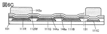
- 1A and 1B are diagrams showing configuration examples of a light emitting device.
- 2A and 2B are diagrams showing configuration examples of a light emitting device.
- 3A and 3B are diagrams showing configuration examples of light emitting devices.
- 4A to 4C are diagrams showing configuration examples of a light emitting device.
- 5A to 5D are diagrams showing configuration examples of the display device.
- 6A to 6F are diagrams illustrating an example of a method for manufacturing a display device.
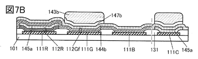
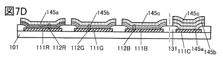
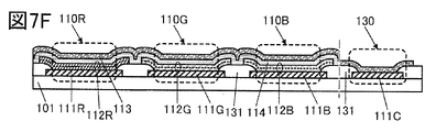
- 7A to 7F are diagrams illustrating an example of a method for manufacturing a display device.
- 8A to 8C are diagrams illustrating an example of a method for manufacturing a display device.
- 9A to 9D are diagrams showing configuration examples of the display device.
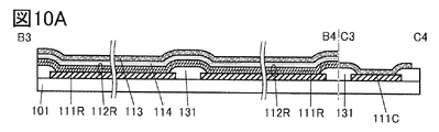
- FIGS. 10A to 10E are diagrams illustrating an example of a method for manufacturing a display device.
- 11A to 11C are diagrams illustrating configuration examples of display devices.
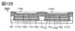
- 12A to 12C are diagrams illustrating configuration examples of display devices.
- 13A to 13C are diagrams showing configuration examples of display devices.
- FIG. 14 is a perspective view showing an example of a display device.
- 15A and 15B are cross-sectional views showing examples of display devices.
- FIG. 16A is a cross-sectional view showing an example of a display device;
- FIG. 16B is a cross-sectional view showing an example of a transistor;
- 17A and 17B are perspective views showing an example of a display module.
- FIG. 18 is a cross-sectional view showing an example of a display device.
- FIG. 16A is a cross-sectional view showing an example of a display device.
- FIG. 16B is a cross-sectional view showing an example of a transistor
- 17A and 17B
- FIG. 19 is a cross-sectional view showing an example of a display device.
- FIG. 20 is a cross-sectional view showing an example of a display device.
- 21A and 21B are diagrams showing configuration examples of a display device.
- 22A and 22B are diagrams illustrating configuration examples of a display device.
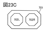
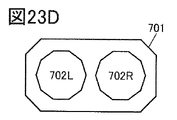
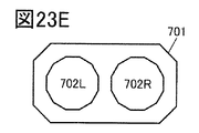
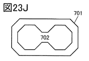
- 23A to 23J are diagrams showing configuration examples of display devices.
- FIG. 24 is a diagram showing a configuration example of a vehicle.
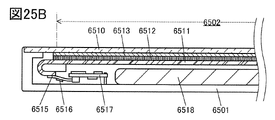
- 25A and 25B are diagrams illustrating examples of electronic devices.
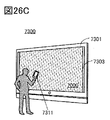
- 26A to 26D are diagrams illustrating examples of electronic devices.
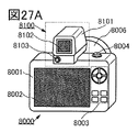
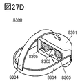
- 27A to 27F are diagrams illustrating examples of electronic devices.
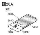
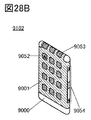
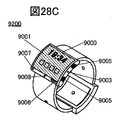
- 28A to 28F are diagrams illustrating examples of electronic devices.
- film and the term “layer” can be interchanged with each other.
- conductive layer or “insulating layer” may be interchangeable with the terms “conductive film” or “insulating film.”
- an EL layer refers to a layer provided between a pair of electrodes of a light-emitting element and containing at least a light-emitting substance (also referred to as a light-emitting layer) or a laminate including a light-emitting layer.
- a display panel which is one aspect of a display device, has a function of displaying (outputting) an image or the like on a display surface. Therefore, the display panel is one aspect of the output device.
- the substrate of the display panel is attached with a connector such as FPC (Flexible Printed Circuit) or TCP (Tape Carrier Package), or an IC is sometimes called a display panel module, a display module, or simply a display panel.
- a connector such as FPC (Flexible Printed Circuit) or TCP (Tape Carrier Package)
- an IC is sometimes called a display panel module, a display module, or simply a display panel.
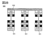
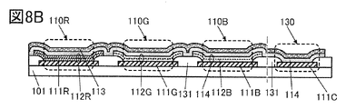
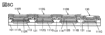
- FIG. 1A shows a schematic cross-sectional view of a light emitting device 500 .
- the light emitting device 500 has a light emitting element 550R that emits red light, a light emitting element 550G that emits green light, and a light emitting element 550B that emits blue light.
- the light-emitting element 550R has a structure in which two light-emitting units (light-emitting unit 512R_1 and light-emitting unit 512R_2) are stacked via an intermediate layer 531 between a pair of electrodes (electrodes 501 and 502).
- the light emitting element 550G has a light emitting unit 512G_1 and a light emitting unit 512G_2
- the light emitting element 550B has a light emitting unit 512B_1 and a light emitting unit 512B_2.
- the electrode 501 functions as a pixel electrode and is provided for each light emitting element.
- the electrode 502 functions as a common electrode and is provided in common to a plurality of light emitting elements.
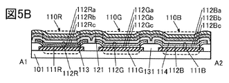
- the light emitting unit 512R_1 has layers 521, 522, 523R, 524, and the like.
- the light-emitting unit 512R_2 includes a layer 522, a light-emitting layer 523R, a layer 524, and the like.
- the light emitting element 550R has a layer 525 and the like between the light emitting unit 512R_2 and the electrode 502. FIG. Note that the layer 525 can also be considered part of the light emitting unit 512R_2.
- the layer 521 has, for example, a layer (hole injection layer) containing a highly hole-injecting substance.
- the layer 522 includes, for example, a layer containing a substance with a high hole-transport property (hole-transport layer).
- the layer 524 includes, for example, a layer containing a highly electron-transporting substance (electron-transporting layer).
- the layer 525 includes, for example, a layer containing a highly electron-injecting substance (electron-injection layer).
- the layer 521 may have an electron-injection layer
- the layer 522 may have an electron-transport layer
- the layer 524 may have a hole-transport layer
- the layer 525 may have a hole-injection layer.
- the layer 522, the light-emitting layer 523R, and the layer 524 may have the same configuration (material, film thickness, etc.) in the light-emitting unit 512R_1 and the light-emitting unit 512R_2, or may have different configurations.
- the present invention is not limited to this.
- the layer 521 has a function of both a hole-injection layer and a hole-transport layer, or when the layer 521 has a function of both an electron-injection layer and an electron-transport layer , the layer 522 may be omitted.
- the intermediate layer 531 has a function of injecting electrons into one of the light-emitting unit 512R_1 and the light-emitting unit 512R_2 and injecting holes into the other when a voltage is applied between the electrodes 501 and 502. .
- the intermediate layer 531 can also be called a charge generation layer.
- the light-emitting layer 523R included in the light-emitting element 550R includes a light-emitting substance that emits red light
- the light-emitting layer 523G included in the light-emitting element 550G includes a light-emitting substance that emits green light
- 523B has a luminescent material that exhibits blue emission.
- the light emitting element 550G and the light emitting element 550B each have a configuration in which the light emitting layer 523R of the light emitting element 550R is replaced with a light emitting layer 523G and a light emitting layer 523B, and other configurations are the same as those of the light emitting element 550R. .
- the layers 521, 522, 524, and 525 may have the same configuration (material, film thickness, etc.) in the light emitting device of each color, or may have different configurations.
- a configuration in which a plurality of light-emitting units are connected in series via an intermediate layer 531, such as the light-emitting element 550R, the light-emitting element 550G, and the light-emitting element 550B, is referred to herein as a tandem structure.
- a structure having one light-emitting unit between a pair of electrodes is called a single structure.
- the tandem structure it is called a tandem structure, but it is not limited to this, and for example, the tandem structure may be called a stack structure.
- a light-emitting element capable of emitting light with high luminance can be obtained by adopting a tandem structure.
- the tandem structure can reduce the current required to obtain the same luminance as compared with the single structure, so reliability can be improved.
- a structure in which a light-emitting layer is separately formed for each light-emitting element, such as the light-emitting element 550R, the light-emitting element 550G, and the light-emitting element 550B, is sometimes called an SBS (side-by-side) structure.
- SBS side-by-side
- the material and structure can be optimized for each light-emitting element, so the degree of freedom in selecting the material and structure increases, and it becomes easy to improve luminance and reliability.
- the light-emitting device 500 of one embodiment of the present invention has a tandem structure and an SBS structure. Therefore, it is possible to have both the merit of the tandem structure and the merit of the SBS structure.
- the light-emitting device 500 of one embodiment of the present invention may be referred to as a two-stage tandem structure because it has a structure in which two light-emitting units are arranged in series as illustrated in FIG. 1A. Further, in the two-stage tandem structure shown in FIG. 1A, the structure is such that the second light-emitting unit having the red light-emitting layer is stacked on the first light-emitting unit having the red light-emitting layer. Similarly, the two-stage tandem structure shown in FIG.
- 1A has a structure in which a second light-emitting unit having a green light-emitting layer is stacked on a first light-emitting unit having a green light-emitting layer, and a blue light-emitting layer is formed.
- a structure is obtained in which the second light-emitting unit having a blue light-emitting layer is stacked on the first light-emitting unit.
- FIG. 1B is a modification of the light emitting device 500 shown in FIG. 1A.
- a light-emitting device 500 shown in FIG. 1B is an example in which a layer 525 is commonly provided between light-emitting elements, like the electrode 502 . At this time, layer 525 can be referred to as a common layer.
- layer 525 can be referred to as a common layer.
- a light-emitting device 500 shown in FIG. 2A is an example in which three light-emitting units are stacked.
- the light-emitting element 550R has a light-emitting unit 512R_3 laminated on the light-emitting unit 512R_2 with an intermediate layer 531 interposed therebetween.
- the light emitting unit 512R_3 has the same configuration as the light emitting unit 512R_2.
- the light emitting unit 512G_3 included in the light emitting element 550G and the light emitting unit 512B_3 included in the light emitting element 550B are similar to the light emitting unit 512R_3.
- FIG. 2B shows an example of stacking n light-emitting units (n is an integer of 2 or more).
- the luminance obtained from the light-emitting element with the same amount of current can be increased according to the number of stacked layers. Further, by increasing the number of stacked light-emitting units, the current required to obtain the same luminance can be reduced, so that the power consumption of the light-emitting element can be reduced according to the number of stacked layers.
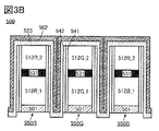
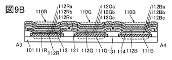
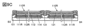
- a light-emitting device 500 shown in FIG. 3A shows an example in which two adjacent light-emitting elements are separated and electrodes 502 are provided along the side surfaces of each light-emitting unit and intermediate layer 531 .
- the intermediate layer 531 and the electrode 502 come into contact with each other, an electrical short may occur. Therefore, it is preferable to insulate the intermediate layer 531 and the electrode 502 .
- FIG. 3A shows an example in which an insulating layer 541 is provided to cover the side surfaces of the electrode 501, each light emitting unit, and the intermediate layer 531.
- the insulating layer 541 can be called a sidewall protective layer, a sidewall insulating film, or the like.
- the intermediate layer 531 and the electrode 502 can be electrically insulated.
- each light-emitting unit and the intermediate layer 531 are preferably perpendicular or substantially perpendicular to the formation surface.
- the angle formed by the surface to be formed and these side surfaces be 60 degrees or more and 90 degrees or less.
- FIG. 3B shows an example where the layer 525 and the electrode 502 are provided along the sides of each light emitting unit and the intermediate layer 531.
- the side wall protective layer has a two-layer structure of an insulating layer 541 and an insulating layer 542 .
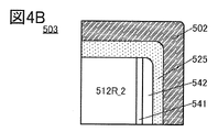
- FIG. 4A is a modification of FIG. 3B.
- 4B is an enlarged view of region 503 shown in FIG. 4A.
- 4A and 3B differ in the shape of the end portion of the insulating layer 542.
- the shape of the end portion of the insulating layer 542 is different, and the layer 525 and the electrode 502 are formed along the shape of the insulating layer 542, so the shapes of the layer 525 and the electrode 502 are also different.
- the thicknesses of the insulating layers 541 and 542 are different between FIG. 4A and FIG. 3B.
- the insulating layer 542 is thicker than the insulating layer 541 .
- the ends of the insulating layer 542 are rounded as shown in FIG.
- the end portion of the insulating layer 542 is rounded as shown in FIG. 4B.
- the coverage of the layer 525 and the electrode 502 is improved, which is preferable.
- the shape of the end portion may be easily rounded.
- the insulating layer 541 (and the insulating layer 542) functioning as a side wall protective layer can prevent electrical short-circuiting between the electrode 502 and the intermediate layer 531.
- electrical short-circuiting between the electrodes 501 and 502 can be prevented. This can prevent electrical short-circuiting at the four corners of the light-emitting element.
- An inorganic insulating film is preferably used for each of the insulating layers 541 and 542 .
- oxides or nitrides can be used, such as silicon oxide, silicon oxynitride, silicon oxynitride, silicon nitride, aluminum oxide, aluminum oxynitride, or hafnium oxide.
- yttrium oxide, zirconium oxide, gallium oxide, tantalum oxide, magnesium oxide, lanthanum oxide, cerium oxide, neodymium oxide, or the like may be used.
- the insulating layer 541 and the insulating layer 542 can be formed by various film forming methods such as sputtering, vapor deposition, CVD (Chemical Vapor Deposition), and ALD (Atomic Layer Deposition).
- the ALD method causes little film formation damage to a layer to be formed
- the insulating layer 541 that is directly formed over the light-emitting unit and the intermediate layer 531 is preferably formed by the ALD method.
- an aluminum oxide film formed by an ALD method can be used for the insulating layer 541, and a silicon nitride film formed by a sputtering method can be used for the insulating layer 542.
- one or both of the insulating layer 541 and the insulating layer 542 have a function as a barrier insulating film against at least one of water and oxygen.
- one or both of the insulating layer 541 and the insulating layer 542 preferably have a function of suppressing diffusion of at least one of water and oxygen.
- one or both of the insulating layer 541 and the insulating layer 542 preferably have a function of trapping or fixing at least one of water and oxygen (also referred to as gettering).
- a barrier insulating film indicates an insulating film having barrier properties.
- barrier property refers to a function of suppressing diffusion of a corresponding substance (also referred to as low permeability).
- the corresponding substance has a function of capturing or fixing (also called gettering).
- Either one or both of the insulating layer 541 and the insulating layer 542 have the function of the barrier insulating film or the gettering function, so that impurities (typically water , or oxygen) can be suppressed. With such a structure, a highly reliable light-emitting device can be provided.
- layer 525 is provided on the sides of each light emitting unit and intermediate layer 531 .
- each light-emitting element can be red, green, blue, cyan, magenta, yellow, white, or the like depending on the material forming the light-emitting layer 523R. Further, the color purity can be further enhanced by providing the light-emitting element with a microcavity structure.
- the light-emitting layer contains two or more kinds of light-emitting substances.
- two or more light-emitting substances may be selected so that the light emission of each light-emitting substance has a complementary color relationship.
- a light-emitting element that emits white light as a whole can be obtained.
- the light-emitting layer preferably contains two or more light-emitting substances that emit light such as R (red), G (green), B (blue), Y (yellow), and O (orange).
- R red
- G green
- B blue
- Y yellow
- O orange
- a light-emitting element has at least a light-emitting layer. Further, in the light-emitting element, layers other than the light-emitting layer include a substance with a high hole-injection property, a substance with a high hole-transport property, a hole-blocking material, a substance with a high electron-transport property, an electron-blocking material, and a substance with a high electron-injection property.
- a layer containing a substance, a bipolar substance (a substance with high electron-transport properties and high hole-transport properties), or the like may be further included.
- Either a low-molecular-weight compound or a high-molecular-weight compound can be used for the light-emitting element, and an inorganic compound may be included.
- Each of the layers constituting the light-emitting element can be formed by a vapor deposition method (including a vacuum vapor deposition method), a transfer method, a printing method, an inkjet method, a coating method, or the like.
- the light-emitting element can be configured to have one or more layers selected from a hole injection layer, a hole transport layer, a hole block layer, an electron block layer, an electron transport layer, and an electron injection layer.
- the hole-injecting layer is a layer that injects holes from the anode into the hole-transporting layer, and contains a material with high hole-injecting properties.
- highly hole-injecting materials include aromatic amine compounds and composite materials containing a hole-transporting material and an acceptor material (electron-accepting material).
- the hole-transporting layer is a layer that transports the holes injected from the anode by the hole-injecting layer to the light-emitting layer.
- a hole-transporting layer is a layer containing a hole-transporting material.
- the hole-transporting material a substance having a hole mobility of 1 ⁇ 10 ⁇ 6 cm 2 /Vs or more is preferable. Note that substances other than these can be used as long as they have a higher hole-transport property than electron-transport property.
- hole-transporting materials include ⁇ -electron-rich heteroaromatic compounds (e.g., carbazole derivatives, thiophene derivatives, furan derivatives, etc.), aromatic amines (compounds having an aromatic amine skeleton), and other highly hole-transporting materials. is preferred.
- ⁇ -electron-rich heteroaromatic compounds e.g., carbazole derivatives, thiophene derivatives, furan derivatives, etc.
- aromatic amines compounds having an aromatic amine skeleton
- other highly hole-transporting materials is preferred.
- the electron transport layer is a layer that transports electrons injected from the cathode by the electron injection layer to the light emitting layer.
- the electron-transporting layer is a layer containing an electron-transporting material.
- an electron-transporting material a substance having an electron mobility of 1 ⁇ 10 ⁇ 6 cm 2 /Vs or more is preferable. Note that substances other than these substances can be used as long as they have a higher electron-transport property than hole-transport property.
- electron-transporting materials include metal complexes having a quinoline skeleton, metal complexes having a benzoquinoline skeleton, metal complexes having an oxazole skeleton, metal complexes having a thiazole skeleton, oxadiazole derivatives, triazole derivatives, imidazole derivatives, ⁇ -electron deficient including oxazole derivatives, thiazole derivatives, phenanthroline derivatives, quinoline derivatives with quinoline ligands, benzoquinoline derivatives, quinoxaline derivatives, dibenzoquinoxaline derivatives, pyridine derivatives, bipyridine derivatives, pyrimidine derivatives, and other nitrogen-containing heteroaromatic compounds
- a material having a high electron transport property such as a type heteroaromatic compound can be used.
- the electron injection layer is a layer that injects electrons from the cathode to the electron transport layer, and is a layer that contains a material with high electron injection properties.
- Alkali metals, alkaline earth metals, or compounds thereof can be used as materials with high electron injection properties.
- a composite material containing an electron-transporting material and a donor material (electron-donating material) can also be used as a material with high electron-injecting properties.
- the electron injection layer examples include lithium, cesium, ytterbium, lithium fluoride (LiF), cesium fluoride (CsF), calcium fluoride (CaF x , X is an arbitrary number), and 8-(quinolinolato)lithium (abbreviation: Liq), 2-(2-pyridyl)phenoratritium (abbreviation: LiPP), 2-(2-pyridyl)-3-pyridinolatritium (abbreviation: LiPPy), 4-phenyl-2-(2-pyridyl)pheno Alkali metals such as latolithium (abbreviation: LiPPP), lithium oxide (LiO x ), cesium carbonate, alkaline earth metals, or compounds thereof can be used.
- the electron injection layer may have a laminated structure of two or more layers. As the laminated structure, for example, lithium fluoride can be used for the first layer and ytterbium can be used for the second layer.
- a material having an electron transport property may be used as the electron injection layer described above.
- a compound having a lone pair of electrons and an electron-deficient heteroaromatic ring can be used as the electron-transporting material.
- a compound having at least one of a pyridine ring, diazine ring (pyrimidine ring, pyrazine ring, pyridazine ring), and triazine ring can be used.
- the lowest unoccupied molecular orbital (LUMO) of the organic compound having an unshared electron pair is preferably -3.6 eV or more and -2.3 eV or less.
- CV cyclic voltammetry
- photoelectron spectroscopy optical absorption spectroscopy
- inverse photoelectron spectroscopy etc. are used to determine the highest occupied molecular orbital (HOMO) level and LUMO level of an organic compound. can be estimated.
- BPhen 4,7-diphenyl-1,10-phenanthroline
- NBPhen 2,9-bis(naphthalen-2-yl)-4,7-diphenyl-1,10-phenanthroline
- HATNA diquinoxalino [2,3-a:2′,3′-c]phenazine
- TmPPPyTz 2,4,6-tris[3′-(pyridin-3-yl)biphenyl-3-yl]-1,3 , 5-triazine
- TmPPPyTz 2,4,6-tris[3′-(pyridin-3-yl)biphenyl-3-yl]-1,3 , 5-triazine
- a light-emitting layer is a layer containing a light-emitting substance.
- the emissive layer can have one or more emissive materials.
- a substance exhibiting emission colors such as blue, purple, violet, green, yellow-green, yellow, orange, and red is used as appropriate.
- a substance that emits near-infrared light can be used as the light-emitting substance.
- Examples of light-emitting substances include fluorescent materials, phosphorescent materials, TADF materials, and quantum dot materials.
- fluorescent materials include pyrene derivatives, anthracene derivatives, triphenylene derivatives, fluorene derivatives, carbazole derivatives, dibenzothiophene derivatives, dibenzofuran derivatives, dibenzoquinoxaline derivatives, quinoxaline derivatives, pyridine derivatives, pyrimidine derivatives, phenanthrene derivatives, and naphthalene derivatives. be done.
- Examples of phosphorescent materials include organometallic complexes (especially iridium complexes) having a 4H-triazole skeleton, 1H-triazole skeleton, imidazole skeleton, pyrimidine skeleton, pyrazine skeleton, or pyridine skeleton, and phenylpyridine derivatives having an electron-withdrawing group.
- organometallic complexes especially iridium complexes
- platinum complexes, rare earth metal complexes, etc. which are used as ligands, can be mentioned.
- the light-emitting layer may contain one or more organic compounds (host material, assist material, etc.) in addition to the light-emitting substance (guest material).
- One or both of a hole-transporting material and an electron-transporting material can be used as the one or more organic compounds.
- Bipolar materials or TADF materials may also be used as one or more organic compounds.
- the light-emitting layer preferably includes, for example, a phosphorescent material and a combination of a hole-transporting material and an electron-transporting material that easily form an exciplex.
- ExTET Exciplex-Triplet Energy Transfer
- a combination that forms an exciplex that emits light that overlaps with the wavelength of the absorption band on the lowest energy side of the light-emitting substance energy transfer becomes smooth and light emission can be efficiently obtained. With this configuration, high efficiency, low-voltage driving, and long life of the light-emitting element can be realized at the same time.
- a material applicable to the electron injection layer such as lithium fluoride
- a material applicable to the hole injection layer can be preferably used.
- a layer containing a hole-transporting material and an acceptor material can be used for the intermediate layer.
- a layer containing an electron-transporting material and a donor material can be used for the intermediate layer.
- the light-emitting material of the light-emitting layer is not particularly limited.
- the light-emitting layer 523R included in the light-emitting unit 512R_1 includes a phosphorescent material
- the light-emitting layer 523R included in the light-emitting unit 512R_2 includes a phosphorescent material
- the light-emitting layer 523G included in the light-emitting unit 512G_1 includes A structure containing a fluorescent material, a light-emitting layer 523G of the light-emitting unit 512G_2 containing a fluorescent material, a light-emitting layer 523B of the light-emitting unit 512B_1 containing a fluorescent material, and a light-emitting layer 523B of the light-emitting unit 512B_2 containing a fluorescent material
- a light-emitting layer 523B of the light-emitting unit 512B_2 containing a fluorescent material
- the light-emitting layer 523R included in the light-emitting unit 512R_1 includes a phosphorescent material
- the light-emitting layer 523R included in the light-emitting unit 512R_2 includes a phosphorescent material
- the light-emitting layer 523G included in the light-emitting unit 512G_1 includes The light-emitting layer 523G of the light-emitting unit 512G_2 contains a phosphorescent material
- the light-emitting layer 523B of the light-emitting unit 512B_1 contains a fluorescent material
- the light-emitting layer 523B of the light-emitting unit 512B_2 contains a fluorescent material. And it is sufficient.
- the display device of one embodiment of the present invention has a structure in which all the light-emitting layers of the light-emitting device 500 illustrated in FIG. 1A include a fluorescent material, or a structure in which all the light-emitting layers of the light-emitting device 500 illustrated in FIG. 1A include a phosphorescent material. may be
- the display device of one embodiment of the present invention is the light-emitting device 500 illustrated in FIG. 1A, in which the light-emitting layer 523R included in the light-emitting unit 512R_1 includes a phosphorescent material, and the light-emitting layer 523R included in the light-emitting unit 512R_2 includes a fluorescent material.
- the light-emitting layer 523R included in the light-emitting unit 512R_1 includes a fluorescent material
- the light-emitting layer 523R included in the light-emitting unit 512R_2 includes a phosphorescent material, that is, a first-level light-emitting layer and a second-level light-emitting layer
- a configuration in which light-emitting materials different from each other are used. Note that although the description here is made for the light emitting units 512R_1 and 512R_2, the same configuration can be applied to the light emitting units 512G_1 and 512G_2 as well as the light emitting units 512B_1 and 512B_2. can.
- This embodiment can be implemented by appropriately combining at least part of it with other embodiments described herein.
- One embodiment of the present invention is a display device including a light-emitting element (also referred to as a light-emitting device).
- the display device has at least two light emitting elements that emit light of different colors.
- Each light-emitting element has a pair of electrodes and an EL layer therebetween.
- the light-emitting element is preferably an organic EL element (organic electroluminescence element).
- Two or more light-emitting elements that emit different colors have EL layers each containing a different material.
- a full-color display device can be realized by using three types of light-emitting elements that emit red (R), green (G), and blue (B) light.
- the EL layer when part or all of the EL layer is separately formed between light emitting elements of different colors, it is known to form by vapor deposition using a shadow mask such as a metal mask.
- a shadow mask such as a metal mask.
- island-like formations occur due to various influences such as precision of the metal mask, misalignment between the metal mask and the substrate, bending of the metal mask, and broadening of the contour of the deposited film due to vapor scattering. Since the shape and position of the organic film deviate from the design, it is difficult to increase the definition and aperture ratio of the display device. Therefore, measures have been taken to artificially increase the definition (also called pixel density) by applying a special pixel arrangement method such as a pentile arrangement.
- an EL layer is processed into a fine pattern without using a shadow mask such as a metal mask.
- a shadow mask such as a metal mask.
- a device manufactured using a metal mask or FMM may be referred to as a device with an MM (metal mask) structure.
- a device manufactured without using a metal mask or FMM may be referred to as a device with an MML (metal maskless) structure.
- a structure in which a light-emitting layer is separately formed or a light-emitting layer is separately painted in each color light-emitting device is referred to as SBS (Side By Side) structure.
- SBS Side By Side
- a light-emitting device capable of emitting white light is sometimes referred to as a white light-emitting device.
- a white light emitting device can be combined with a colored layer (for example, a color filter) to realize a full-color display device.
- an EL layer has a tandem structure (also referred to as a stack structure) in which light-emitting units are stacked with an intermediate layer interposed therebetween. Accordingly, compared to a configuration having one light-emitting unit, the current required for light emission with the same luminance can be reduced, so that power consumption can be reduced and deterioration can be greatly suppressed. In addition, since the luminance can be significantly increased when the same current is applied, it can be suitably used for electronic devices that require high luminance.
- a first EL film and a first mask film are laminated to cover two pixel electrodes.
- a resist mask is formed on the first mask film at a position overlapping with one pixel electrode (first pixel electrode).
- part of the first mask film and part of the first EL film are etched. At this time, the etching is finished when the other pixel electrode (second pixel electrode) is exposed.
- a part of the first EL film also referred to as a first EL layer
- a part of the mask film (also referred to as a first sacrificial layer) can be formed on the first pixel electrode.
- a second EL film and a second mask film are laminated and formed.
- a resist mask is formed at a position overlapping with the second pixel electrode.
- a portion of the second sacrificial film that does not overlap the resist mask and a portion of the second EL film are etched in the same manner as described above. Accordingly, a first EL layer and a first mask layer are formed on the first pixel electrode, and a second EL layer and a second mask layer (a second sacrificial layer) are formed on the second pixel electrode. ) are respectively provided. In this manner, the first EL layer and the second EL layer can be separately formed. Finally, the first mask layer and the second mask layer are removed to expose the first EL layer and the second EL layer, and then a common electrode is formed to form a two-color light emitting element. can be separated.
- EL layers of light emitting elements of three or more colors can be separately formed, and a display device having light emitting elements of three or four or more colors can be realized.
- an electrode also referred to as a first electrode, a connection electrode, or the like
- the connection electrode is arranged outside the display portion where the pixel is provided.
- the first mask layer also on the connection electrode.
- it is preferable to provide a second mask layer on the connection electrode. The first mask layer and the second mask layer provided on the connection electrode are etched simultaneously with the first mask layer on the first EL layer and the second mask layer on the second EL layer. can be removed.
- the gap can be narrowed to 500 nm or less, 200 nm or less, 100 nm or less, or even 50 nm or less.
- the aperture ratio can be brought close to 100%.
- the aperture ratio can be 50% or more, 60% or more, 70% or more, 80% or more, or even 90% or more, and less than 100%.
- the pattern of the EL layer itself can also be made much smaller than when a metal mask is used.
- the thickness varies between the center and the edge of the pattern, so the effective area that can be used as the light emitting region is smaller than the area of the entire pattern. .
- the pattern is formed by processing a film formed to have a uniform thickness, the thickness can be made uniform within the pattern, and even if the pattern is fine, almost the entire area of the pattern can emit light. It can be used as a region. Therefore, according to the above manufacturing method, both high definition and high aperture ratio can be achieved.
- an insulating layer between two adjacent pixel electrodes.
- the insulating layer is provided to cover the edge of the pixel electrode. A region on the pixel electrode covered with the insulating layer does not function as a light emitting region of the light emitting element. can increase
- the end (side surface) of the EL layer is located on the insulating layer.
- the ends (side surfaces) of the two EL layers are arranged to face each other on the insulating layer. The narrower the gap between the two EL layers, the narrower the width of the insulating layer, so that the aperture ratio of the display device can be increased.
- a display device in which fine light-emitting elements are integrated since a display device in which fine light-emitting elements are integrated can be realized, it is necessary to apply a special pixel arrangement method such as a pentile method to artificially increase the definition. There is no Therefore, a display device with a so-called stripe arrangement in which R, G, and B are arranged in one direction and a resolution of 500 ppi or more, 1000 ppi or more, or 2000 ppi or more, furthermore 3000 ppi or more, furthermore 5000 ppi or more is realized. be able to. Furthermore, it is possible to realize a display device with an effective light emitting area ratio (aperture ratio) of 50% or more, further 60% or more, further 70% or more and less than 100%.
- the effective light emitting area ratio refers to the ratio of the area of a region that can be regarded as a light emitting region in one pixel to the area of one pixel calculated from the pixel repetition pitch of the display device.
- FIG. 5A shows a schematic top view of the display device 100 of one embodiment of the present invention.
- the display device 100 includes a plurality of light emitting elements 110R that emit red, a plurality of light emitting elements 110G that emit green, and a plurality of light emitting elements 110B that emit blue.
- the light-emitting region of each light-emitting element is labeled with R, G, and B. As shown in FIG.
- the light emitting elements 110R, 110G, and 110B are arranged in a matrix.
- FIG. 5A shows a so-called stripe arrangement in which light emitting elements of the same color are arranged in one direction. Note that the arrangement method of the light emitting elements is not limited to this, and an arrangement method such as a delta arrangement or a zigzag arrangement may be applied, or a pentile arrangement may be used.
- the light emitting elements 110R, 110G, and 110B are arranged in the X direction. In addition, light emitting elements of the same color are arranged in the Y direction intersecting with the X direction.
- EL elements such as OLEDs (Organic Light Emitting Diodes) or QLEDs (Quantum-dot Light Emitting Diodes) are preferably used as the light emitting elements 110R, 110G, and 110B.
- the light-emitting substance of the EL element include a substance that emits fluorescence (fluorescent material), a substance that emits phosphorescence (phosphorescence material), and a substance that exhibits thermally activated delayed fluorescence (thermally activated delayed fluorescence (TADF) material). ) and the like.
- TADF thermally activated delayed fluorescence
- a light-emitting substance included in an EL element not only an organic compound but also an inorganic compound (such as a quantum dot material) can be used.
- FIG. 5B is a schematic cross-sectional view corresponding to the dashed-dotted line A1-A2 in FIG. 5A
- FIG. 5C is a schematic cross-sectional view corresponding to the dashed-dotted line B1-B2.
- FIG. 5B shows cross sections of the light emitting element 110R, the light emitting element 110G, and the light emitting element 110B.
- the light emitting element 110R has a pixel electrode 111R, an EL layer 112R, an EL layer 114, and a common electrode 113.
- the light emitting element 110G has a pixel electrode 111G, an EL layer 112G, an EL layer 114, and a common electrode 113.
- the light-emitting element 110B has a pixel electrode 111B, an EL layer 112B, an EL layer 114, and a common electrode 113.
- the EL layer 114 and the common electrode 113 are commonly provided for the light emitting elements 110R, 110G, and 110B.
- the EL layer 114 can also be called a common layer.
- the EL layer 112R of the light-emitting element 110R contains a light-emitting organic compound that emits light having an intensity in at least the red wavelength range.
- the EL layer 112G included in the light-emitting element 110G contains a light-emitting organic compound that emits light having an intensity in at least the green wavelength range.
- the EL layer 112B included in the light-emitting element 110B contains a light-emitting organic compound that emits light having an intensity in at least a blue wavelength range.
- Each of the EL layer 112R, the EL layer 112G, and the EL layer 112B includes a layer containing a light-emitting organic compound (light-emitting layer), an electron injection layer, an electron transport layer, a hole injection layer, and a hole transport layer. You may have one or more of them.
- the EL layer 114 can have a structure without a light-emitting layer.
- the EL layer 114 has one or more of an electron injection layer, an electron transport layer, a hole injection layer, and a hole transport layer.
- the light emitting element having the tandem structure illustrated in Embodiment 1 can be applied to the light emitting element 110R, the light emitting element 110G, and the light emitting element 110B.
- the EL layer 112R included in the light-emitting element 110 includes a light-emitting unit 112Ra, an intermediate layer 112Rb, and a light-emitting unit 112Rc.
- FIGS. 5B and 5C the same hatching pattern is given to the light emitting unit 112Ra and the light emitting unit 112Rc, and the intermediate layer 112Rb is indicated by a dashed line.
- EL layer 112G has light-emitting unit 112Ga, intermediate layer 112Gb, and light-emitting unit 112Gc
- EL layer 112B has light-emitting unit 112Ba, intermediate layer 112Bb, and light-emitting unit 112Bc.
- an insulating layer functioning as a sidewall protective layer may be provided in contact with side surfaces of the EL layer 112R, the EL layer 112G, and the EL layer 112B.
- a pixel electrode 111R, a pixel electrode 111G, and a pixel electrode 111B are provided for each light emitting element. Further, the common electrode 113 and the EL layer 114 are provided as a continuous layer common to each light emitting element.
- a conductive film having a property of transmitting visible light is used for one of the pixel electrodes and the common electrode 113, and a conductive film having a reflective property is used for the other.
- An insulating layer 131 is provided to cover end portions of the pixel electrode 111R, the pixel electrode 111G, and the pixel electrode 111B.
- the ends of the insulating layer 131 are preferably tapered. Note that the insulating layer 131 may be omitted if unnecessary.
- the tapered end of the object means that the angle formed by the surface and the surface to be formed in the region of the end is greater than 0 degrees and less than 90 degrees, preferably 5 degrees or more. It refers to having a cross-sectional shape that is 70 degrees or less and that the thickness increases continuously from the end.
- Each of the EL layer 112R, the EL layer 112G, and the EL layer 112B has a region in contact with the upper surface of the pixel electrode and a region in contact with the surface of the insulating layer 131.
- end portions of the EL layer 112R, the EL layer 112G, and the EL layer 112B are located over the insulating layer 131 .
- a gap is provided between the two EL layers between the light emitting elements of different colors.
- the EL layer 112R, the EL layer 112G, and the EL layer 112B are preferably provided so as not to be in contact with each other. This can suitably prevent current from flowing through two adjacent EL layers and causing unintended light emission. Therefore, the contrast can be increased, and a display device with high display quality can be realized.
- the EL layers 112R are formed in strips so that the EL layers 112R are continuous in the Y direction.
- the EL layer 112R and the like are formed in strips so that the EL layers 112R are continuous in the Y direction.
- a space for dividing them is not required, and the area of the non-light-emitting region between the light-emitting elements can be reduced, so that the aperture ratio can be increased.
- FIG. 5C shows the cross section of the light emitting element 110R as an example, but the light emitting elements 110G and 110B can also have the same shape.
- a protective layer 121 is provided on the common electrode 113 to cover the light emitting elements 110R, 110G, and 110B.
- the protective layer 121 has a function of preventing impurities such as water from diffusing into each light emitting element from above.
- the protective layer 121 can have, for example, a single layer structure or a laminated structure including at least an inorganic insulating film.
- inorganic insulating films include oxide films and nitride films such as silicon oxide films, silicon oxynitride films, silicon nitride oxide films, silicon nitride films, aluminum oxide films, aluminum oxynitride films, and hafnium oxide films.
- a semiconductor material such as indium gallium oxide or indium gallium zinc oxide may be used for the protective layer 121 .
- the protective layer 121 a laminated film of an inorganic insulating film and an organic insulating film can be used.
- a structure in which an organic insulating film is sandwiched between a pair of inorganic insulating films is preferable.
- the organic insulating film functions as a planarizing film. As a result, the upper surface of the organic insulating film can be flattened, so that the coverage of the inorganic insulating film thereon can be improved, and the barrier property can be enhanced.
- the upper surface of the protective layer 121 is flat, when a structure (for example, a color filter, an electrode of a touch sensor, or a lens array) is provided above the protective layer 121, an uneven shape due to the structure below may be formed. This is preferable because it can reduce the impact.
- a structure for example, a color filter, an electrode of a touch sensor, or a lens array
- FIG. 5A also shows a connection electrode 111C electrically connected to the common electrode 113.
- FIG. 111 C of connection electrodes are given the electric potential (for example, anode electric potential or cathode electric potential) for supplying to the common electrode 113.
- FIG. The connection electrode 111C is provided outside the display area where the light emitting elements 110R and the like are arranged. Also, in FIG. 5A, the common electrode 113 is indicated by a dashed line.
- connection electrodes 111C can be provided along the periphery of the display area. For example, it may be provided along one side of the periphery of the display area, or may be provided over two or more sides of the periphery of the display area. That is, when the top surface shape of the display area is rectangular, the top surface shape of the connection electrode 111C can be strip-shaped, L-shaped, U-shaped (square bracket-shaped), square, or the like.
- FIG. 5D is a schematic cross-sectional view corresponding to the dashed-dotted line C1-C2 in FIG. 5A.
- FIG. 5D shows a connection portion 130 where the connection electrode 111C and the common electrode 113 are electrically connected.
- the common electrode 113 is provided on the connection electrode 111 ⁇ /b>C so as to be in contact therewith, and the protective layer 121 is provided to cover the common electrode 113 .
- An insulating layer 131 is provided to cover the end of the connection electrode 111C.
- the thin films (insulating film, semiconductor film, conductive film, etc.) that make up the display device can be formed by sputtering, chemical vapor deposition (CVD), vacuum deposition, pulsed laser deposition (PLD). ) method, Atomic Layer Deposition (ALD) method, or the like.
- the CVD method includes a plasma enhanced CVD (PECVD) method, a thermal CVD method, and the like. Also, one of the thermal CVD methods is the metal organic CVD (MOCVD) method.
- the thin films (insulating films, semiconductor films, conductive films, etc.) that make up the display device can be applied by spin coating, dipping, spray coating, inkjet, dispensing, screen printing, offset printing, doctor knife method, slit coating, roll coating, curtain coating, etc. It can be formed by a method such as coating or knife coating.
- the thin film when processing the thin film that constitutes the display device, a photolithography method or the like can be used.
- the thin film may be processed by a nanoimprint method, a sandblast method, a lift-off method, or the like.
- an island-shaped thin film may be directly formed by a film formation method using a shielding mask such as a metal mask.
- a photolithography method there are typically the following two methods.
- One is a method of forming a resist mask on a thin film to be processed, processing the thin film by etching or the like, and removing the resist mask.
- the other is a method of forming a photosensitive thin film, then performing exposure and development to process the thin film into a desired shape.
- the light used for exposure can be i-line (wavelength 365 nm), g-line (wavelength 436 nm), h-line (wavelength 405 nm), or a mixture thereof.
- ultraviolet rays, KrF laser light, ArF laser light, or the like can also be used.
- the exposure may be performed by an immersion exposure technique.
- extreme ultraviolet (EUV) light, X-rays, or the like may be used.
- An electron beam can also be used instead of the light used for exposure. The use of extreme ultraviolet light, X-rays, or electron beams is preferable because extremely fine processing is possible.
- a photomask is not necessary when exposure is performed by scanning a beam such as an electron beam.
- a dry etching method, a wet etching method, a sandblasting method, or the like can be used to etch the thin film.
- substrate 101 a substrate having heat resistance enough to withstand at least heat treatment performed later can be used.
- a substrate having heat resistance enough to withstand at least heat treatment performed later can be used.
- a substrate having heat resistance enough to withstand at least heat treatment performed later can be used.
- a glass substrate, a quartz substrate, a sapphire substrate, a ceramic substrate, an organic resin substrate, or the like can be used.
- a semiconductor substrate such as a single crystal semiconductor substrate made of silicon, silicon carbide, or the like, a polycrystalline semiconductor substrate, a compound semiconductor substrate such as silicon germanium, or an SOI substrate can be used.
- the substrate 101 it is preferable to use a substrate in which a semiconductor circuit including a semiconductor element such as a transistor is formed on the above semiconductor substrate or insulating substrate.
- the semiconductor circuit preferably constitutes, for example, a pixel circuit, a gate line driver circuit (gate driver), a source line driver circuit (source driver), and the like.
- gate driver gate line driver
- source driver source driver
- an arithmetic circuit, a memory circuit, and the like may be configured.
- a pixel electrode 111R, a pixel electrode 111G, a pixel electrode 111B, and a connection electrode 111C are formed on the substrate 101.
- a conductive film to be a pixel electrode and a connection electrode is formed, a resist mask is formed by photolithography, and unnecessary portions of the conductive film are removed by etching. After that, by removing the resist mask, the pixel electrode 111R, the pixel electrode 111G, the pixel electrode 111B, and the connection electrode 111C can be formed.
- each pixel electrode When a conductive film that reflects visible light is used as each pixel electrode, it is preferable to use a material (for example, silver or aluminum) that has as high a reflectance as possible over the entire wavelength range of visible light. Thereby, not only can the light extraction efficiency of the light emitting element be improved, but also the color reproducibility can be improved.
- a material for example, silver or aluminum
- an insulating layer 131 is formed to cover end portions of the pixel electrode 111R, the pixel electrode 111G, the pixel electrode 111B, and the connection electrode 111C (FIG. 6A).
- an organic insulating film or an inorganic insulating film can be used as the insulating layer 131.
- the insulating layer 131 preferably has a tapered end in order to improve the step coverage of the subsequent EL film.
- the EL film 112Rf has a film containing at least a luminescent compound.
- one or more of films functioning as an electron injection layer, an electron transport layer, a charge generation layer, a hole transport layer, or a hole injection layer may be stacked.
- the EL film 112Rf can be formed, for example, by a vapor deposition method, a sputtering method, an inkjet method, or the like. Note that the method is not limited to this, and the film forming method described above can be used as appropriate.
- the EL film 112Rf is preferably a laminated film in which a hole injection layer, a hole transport layer, a light emitting layer, and an electron transport layer are laminated in this order.
- a film having an electron-injection layer can be used as the EL layer 114 to be formed later.
- the light-emitting layer can be prevented from being damaged in a later photolithography step or the like, and a highly reliable light-emitting element can be manufactured.
- an electron-transporting organic compound can be used for the electron-transporting layer, and a material containing the organic compound and a metal can be used for the electron-injecting layer.
- the EL film 112Rf is preferably formed so as not to be provided on the connection electrode 111C.
- the EL film 112Rf is formed by a vapor deposition method (or a sputtering method)
- a mask film 144a is formed to cover the EL film 112Rf. Also, the mask film 144a is provided in contact with the upper surface of the connection electrode 111C.
- the mask film 144a a film having high resistance to the etching process of each EL film such as the EL film 112Rf, that is, a film having a high etching selectivity can be used. Also, the mask film 144a can use a film having a high etching selectivity with respect to a protective film such as a protective film 146a to be described later. Furthermore, as the mask film 144a, a film that can be removed by a wet etching method that causes little damage to each EL film can be used.
- the mask film 144a for example, an inorganic film such as a metal film, an alloy film, a metal oxide film, a semiconductor film, or an inorganic insulating film can be used.
- the mask film 144a can be formed by various film forming methods such as a sputtering method, a vapor deposition method, a CVD method, and an ALD method.
- the ALD method causes little film formation damage to the layer to be formed
- the mask film 144a that is directly formed on the EL film 112Rf is preferably formed using the ALD method.
- metal materials such as gold, silver, platinum, magnesium, nickel, tungsten, chromium, molybdenum, iron, cobalt, copper, palladium, titanium, aluminum, yttrium, zirconium, and tantalum, or the metal materials can be used.
- a low melting point material such as aluminum or silver.
- a metal oxide such as indium gallium zinc oxide (In--Ga--Zn oxide, also referred to as IGZO) can be used.
- indium oxide, indium zinc oxide (In—Zn oxide), indium tin oxide (In—Sn oxide), indium titanium oxide (In—Ti oxide), indium tin zinc oxide (In—Sn -Zn oxide), indium titanium zinc oxide (In-Ti-Zn oxide), indium gallium tin zinc oxide (In-Ga-Sn-Zn oxide), and the like can be used.
- indium tin oxide containing silicon or the like can be used.
- element M is aluminum, silicon, boron, yttrium, copper, vanadium, beryllium, titanium, iron, nickel, germanium, zirconium, molybdenum, lanthanum, cerium, neodymium, hafnium, tantalum, tungsten , or one or more selected from magnesium).
- M is preferably one or more selected from gallium, aluminum, and yttrium.
- Inorganic insulating materials such as aluminum oxide, hafnium oxide, and silicon oxide can be used as the mask film 144a.
- a material that can be dissolved in a solvent that is chemically stable with respect to at least the film positioned at the top of the EL film 112Rf as the mask film 144a.
- a material that dissolves in water or alcohol can be suitably used for the mask film 144a.
- wet film formation methods that can be used to form the mask film 144a include spin coating, dipping, spray coating, inkjet, dispensing, screen printing, offset printing, doctor knife method, slit coating, roll coating, curtain coating, and knife coating. There are coats.
- an organic material such as polyvinyl alcohol (PVA), polyvinyl butyral, polyvinylpyrrolidone, polyethylene glycol, polyglycerin, pullulan, water-soluble cellulose, or alcohol-soluble polyamide resin can be used.
- the protective film 146a is a film used as a hard mask when etching the mask film 144a later. Moreover, the mask film 144a is exposed when the protective film 146a is processed later. Therefore, the mask film 144a and the protective film 146a are selected from a combination of films having a high etching selectivity. Therefore, a film that can be used for the protective film 146a can be selected according to the etching conditions for the mask film 144a and the etching conditions for the protective film 146a.
- a gas containing fluorine also referred to as a fluorine-based gas
- An alloy containing molybdenum and niobium, an alloy containing molybdenum and tungsten, or the like can be used for the protective film 146a.
- metal oxide films such as IGZO and ITO are used. and can be used for the mask film 144a.
- the protective film 146a is not limited to this, and can be selected from various materials according to the etching conditions of the mask film 144a and the protective film 146a. For example, it can be selected from films that can be used for the mask film 144a.
- a nitride film for example, can be used as the protective film 146a.
- nitrides such as silicon nitride, aluminum nitride, hafnium nitride, titanium nitride, tantalum nitride, tungsten nitride, gallium nitride, and germanium nitride can also be used.
- an oxide film and an oxynitride film can be used as the protective film 146a.
- an oxide film or an oxynitride film such as silicon oxide, silicon oxynitride, aluminum oxide, aluminum oxynitride, hafnium oxide, or hafnium oxynitride can be used.
- an inorganic insulating material such as aluminum oxide, hafnium oxide, or silicon oxide formed by ALD is used, and as the protective film 146a, indium gallium zinc oxide (In—Ga—Zn It is preferable to use a metal oxide containing indium such as an oxide (also referred to as IGZO).
- an organic film that can be used for the EL film 112Rf or the like may be used as the protective film 146a.
- the same organic film as used for the EL film 112Rf, the EL film 112Gf, or the EL film 112Bf can be used for the protective film 146a.
- a deposition apparatus can be used in common with the EL film 112Rf and the like, which is preferable.
- a resist mask 143a is formed on the protective film 146a at a position overlapping with the pixel electrode 111R and at a position overlapping with the connection electrode 111C (FIG. 6C).
- the resist mask 143a can use a resist material containing a photosensitive resin, such as a positive resist material or a negative resist material.
- the EL film 112Rf is dissolved by the solvent of the resist material. There is a risk of Such a problem can be prevented by using the protective film 146a.
- the resist mask 143a may be formed directly on the mask film 144a without using the protective film 146a.
- etching the protective film 146a it is preferable to use etching conditions with a high selectivity so that the mask film 144a is not removed by the etching.
- Etching of the protective film 146a can be performed by wet etching or dry etching. By using dry etching, reduction of the pattern of the protective film 146a can be suppressed.
- the removal of the resist mask 143a can be performed by wet etching or dry etching.
- the resist mask 143a is preferably removed by dry etching (also referred to as plasma ashing) using an oxygen gas as an etching gas.
- the resist mask 143a is removed while the EL film 112Rf is covered with the mask film 144a, the influence on the EL film 112Rf is suppressed.
- the EL film 112Rf is exposed to oxygen, the electrical characteristics may be adversely affected, so it is suitable for etching using oxygen gas such as plasma ashing.
- the etching of the mask film 144a can be performed by wet etching or dry etching, but it is preferable to use a dry etching method because it can suppress pattern shrinkage.
- Etching the EL film 112Rf and the protective layer 147a by the same treatment is preferable because the process can be simplified and the manufacturing cost of the display device can be reduced.
- the EL film 112Rf is preferably etched by dry etching using an etching gas that does not contain oxygen as its main component.
- Etching gases containing no oxygen as a main component include, for example, noble gases such as CF 4 , C 4 F 8 , SF 6 , CHF 3 , Cl 2 , H 2 O, BCl 3 , H 2 and He.
- a mixed gas of the above gas and a diluent gas that does not contain oxygen can be used as an etching gas.
- the etching of the EL film 112Rf and the etching of the protective layer 147a may be performed separately. At this time, the EL film 112Rf may be etched first, or the protective layer 147a may be etched first.
- the EL layer 112R and the connection electrode 111C are covered with the mask layer 145a.
- the above description of the EL film 112Rf can be used.
- a mask film 144b is formed on the EL film 112Gf.
- the mask film 144b can be formed by the same method as the mask film 144a. In particular, it is preferable to use the same material as the mask film 144a for the mask film 144b.
- a mask film 144a is formed on the connection electrode 111C to cover the mask layer 145a.
- a protective film 146b is formed on the mask film 144b.
- the protective film 146b can be formed by the same method as the protective film 146a. In particular, it is preferable to use the same material as the protective film 146a for the protective film 146b.
- a resist mask 143b is formed on the protective film 146b in a region overlapping with the pixel electrode 111G and a region overlapping with the connection electrode 111C (FIG. 7A).
- the resist mask 143b can be formed by a method similar to that of the resist mask 143a.
- the description of the protective film 146a can be used.
- the description of the mask film 144a can be used.
- the description of the EL film 112Rf and the protective layer 147a can be used.
- the EL layer 112R is protected by the mask layer 145a, it can be prevented from being damaged in the etching process of the EL film 112Gf.
- the strip-shaped EL layer 112R and the strip-shaped EL layer 112G can be separately manufactured with high positional accuracy.
- the EL layer 112G After forming the EL layer 112G, the EL film 112Bf, the mask film 144c, the protective film 146c, and the resist mask 143c (all not shown) are formed in order. Subsequently, after etching the protective film 146c to form a protective layer 147c (not shown), the resist mask 143c is removed. Subsequently, the mask film 144c is etched to form a mask layer 145c. After that, the protective layer 147c and the EL film 112Bf are etched to form the strip-shaped EL layer 112B.
- a mask layer 145c is also formed on the connection electrode 111C at the same time.
- a mask layer 145a, a mask layer 145b, and a mask layer 145c are laminated on the connection electrode 111C.
- the mask layers 145a, 145b, and 145c can be removed by wet etching or dry etching. At this time, it is preferable to use a method that damages the EL layer 112R, the EL layer 112G, and the EL layer 112B as little as possible. In particular, it is preferable to use a wet etching method. For example, it is preferable to use wet etching using a tetramethylammonium hydroxide aqueous solution (TMAH), dilute hydrofluoric acid, oxalic acid, phosphoric acid, acetic acid, nitric acid, or a mixed liquid thereof.
- TMAH tetramethylammonium hydroxide aqueous solution
- the mask layers 145a, 145b, and 145c by dissolving them in a solvent such as water or alcohol.
- a solvent such as water or alcohol.
- various alcohols such as ethyl alcohol, methyl alcohol, isopropyl alcohol (IPA), and glycerin can be used as the alcohol capable of dissolving the mask layers 145a, 145b, and 145c.
- drying treatment is performed in order to remove water contained inside the EL layers 112R, 112G, and 112B and water adsorbed to the surfaces thereof.
- heat treatment is preferably performed in an inert gas atmosphere or a reduced pressure atmosphere.
- the heat treatment can be performed at a substrate temperature of 50° C. to 200° C., preferably 60° C. to 150° C., more preferably 70° C. to 120° C.
- a reduced-pressure atmosphere is preferable because drying can be performed at a lower temperature.
- the EL layer 112R, the EL layer 112G, and the EL layer 112B can be produced separately.
- the EL layer 114 is formed to cover the EL layer 112R, the EL layer 112G, and the EL layer 112B.
- the EL layer 114 can be formed by the same method as the EL film 112Rf. When the EL layer 114 is formed by vapor deposition, it is preferable to use a shielding mask so that the EL layer 114 is not formed on the connection electrode 111C.
- the common electrode 113 can be formed by a film forming method such as vapor deposition or sputtering. Alternatively, a film formed by an evaporation method and a film formed by a sputtering method may be stacked. At this time, it is preferable to form the common electrode 113 so as to include the region where the EL layer 114 is formed. That is, a structure in which an end portion of the EL layer 114 overlaps with the common electrode 113 can be employed.
- the common electrode 113 is preferably formed using a shielding mask.
- the common electrode 113 is electrically connected to the connection electrode 111C outside the display area.
- a protective layer 121 is formed over the common electrode 113 .
- a sputtering method, a PECVD method, or an ALD method is preferably used for forming the inorganic insulating film used for the protective layer 121 .
- the ALD method is preferable because it has excellent step coverage and hardly causes defects such as pinholes.
- the display device 100 shown in FIGS. 5B and 5C can be manufactured.
- the common electrode 113 and the EL layer 114 are formed so as to have different upper surface shapes is shown, but they may be formed in the same region.
- FIG. 8A shows a schematic cross-sectional view after removing the mask layer in the above. Subsequently, as shown in FIG. 8B, an EL layer 114 and a common electrode 113 are formed using the same shielding mask or without using a shielding mask. This can reduce manufacturing costs compared to using different shielding masks.
- the EL layer 114 is sandwiched between the connection electrode 111C and the common electrode 113 in the connection portion 130 .
- a protective layer 121 is formed.
- Configuration example 2 A configuration example of a display device that is partially different from configuration example 1 will be described below. In the following, explanations of parts that overlap with the above may be omitted.
- a display device 100A shown in FIGS. 9A to 9D differs from the display device 100 described above mainly in that the shapes of the EL layer 114 and the common electrode 113 are different.
- the EL layer 112R, the EL layer 114, and the common electrode 113 are separated between the two light emitting elements 110R in the Y-direction cross section.
- the EL layer 112 ⁇ /b>R, the EL layer 114 , and the common electrode 113 have end portions overlapping with the insulating layer 131 .
- the protective layer 121 is provided to cover the side surfaces of the EL layer 112R, the EL layer 114, and the common electrode 113 in a region overlapping with the insulating layer 131.
- a concave portion may be formed in a part of the upper surface of the insulating layer 131 .
- the protective layer 121 is provided along the surface of the concave portion of the insulating layer 131 so as to be in contact therewith. This is preferable because the contact area between the insulating layer 131 and the protective layer 121 is increased and the adhesion between them is improved.
- FIG. 9A outlines of the common electrode 113 and the EL layer 114 are indicated by dashed lines.
- the common electrode 113 and the EL layer 114 each have a belt-like top surface shape whose longitudinal direction is parallel to the X direction.
- the EL layer 112R has an island shape.
- the light emitting element 110G and the light emitting element 110B can also have the same configuration.
- FIG. 10A to 10D show schematic cross-sectional views in each step illustrated below.
- the cross section corresponding to the dashed-dotted line B3-B4 in FIG. 9A and the cross section corresponding to the dashed-dotted line C3-C4 are shown side by side.
- a plurality of resist masks 143 d are formed on the common electrode 113 .
- the resist mask 143d is formed to have a belt-like top surface shape extending in the X direction.
- the resist mask 143d overlaps with the pixel electrode 111R.
- An end portion of the resist mask 143 d is provided on the insulating layer 131 .
- the etching is preferably performed by dry etching.
- a part of the insulating layer 131 may be etched during etching of the common electrode 113, the EL layer 114, and the EL layer 112R, and a recess may be formed in the upper portion of the insulating layer 131 as shown in FIG. 10C.
- a portion of the insulating layer 131 not covered with the resist mask 143d may be etched and divided into two.
- the resist mask 143d is removed.
- the removal of the resist mask 143d can be performed by wet etching or dry etching.
- a protective layer 121 is formed (FIG. 10D).
- the protective layer 121 is provided to cover the side surface of the common electrode 113, the side surface of the EL layer 114, and the side surface of the EL layer 112R. Moreover, the protective layer 121 is preferably provided in contact with the upper surface of the insulating layer 131 .
- a gap (also referred to as gap, space, etc.) 122 may be formed above the insulating layer 131 when the protective layer 121 is formed.
- the air gap 122 may be under reduced pressure or at atmospheric pressure.
- the gap 122 may contain a gas such as air, nitrogen, or noble gas, or a film-forming gas used for film-forming the protective layer 121 .
- the resist mask 143 d is directly formed on the common electrode 113 here, a film functioning as a hard mask may be provided on the common electrode 113 .
- a hard mask is formed using the resist mask 143d as a mask, and after removing the resist mask, the common electrode 113, the EL layer 114, the EL layer 112R, and the like can be etched using the hard mask as a mask. At this time, the hard mask may be removed or left.
- FIG. 11A and 11B show schematic cross-sectional views of the display device 100B.
- a top view of the display device 100B is the same as in FIG. 5A.
- 11A corresponds to the cross section in the X direction
- FIG. 11B corresponds to the cross section in the Y direction.
- the display device 100B differs from the display device 100 mainly in that it does not have the EL layer 114, which is a common layer.
- the common electrode 113 is provided in contact with the upper surfaces of the EL layer 112R, the EL layer 112G, and the EL layer 112B.
- the light-emitting element 110R, the light-emitting element 110G, and the light-emitting element 110B can each have a completely different stacked structure, which increases the choice of materials, thus increasing the degree of freedom in design. can.
- a display device 100C shown in FIG. 11C is an example in which a slit extending in the X direction is formed in a region of the common electrode 113 overlapping the insulating layer 131, like the display device 100A.
- the protective layer 121 is provided in contact with the side surface of the common electrode 113 , the side surface of the EL layer 112 ⁇ /b>R, and the upper surface of the insulating layer 131 .
- a display device 100D shown in FIGS. 12A and 12B is different from the display device 100 described above mainly in the configuration of the light-emitting elements.
- the light emitting element 110R has an optical adjustment layer 115R between the pixel electrode 111R and the EL layer 112R.
- the light emitting element 110G has an optical adjustment layer 115G between the pixel electrode 111G and the EL layer 112G.
- the light emitting element 110B has an optical adjustment layer 115B between the pixel electrode 111B and the EL layer 112B.
- the optical adjustment layer 115R, the optical adjustment layer 115G, and the optical adjustment layer 115B each have transparency to visible light.
- the optical adjustment layer 115R, the optical adjustment layer 115G, and the optical adjustment layer 115B have different thicknesses. Thereby, the optical path length can be varied for each light emitting element.
- each light emitting element has a so-called microcavity structure (microresonator structure), and light of a specific wavelength is enhanced. Thereby, a display device with improved color purity can be realized.
- a conductive material that is transparent to visible light can be used for each optical adjustment layer.
- conductive oxides such as indium oxide, indium tin oxide, indium zinc oxide, zinc oxide, gallium-containing zinc oxide, silicon-containing indium tin oxide, and silicon-containing indium zinc oxide can be used. .
- Each optical adjustment layer can be formed after forming the pixel electrode 111R, the pixel electrode 111G, and the pixel electrode 111B and before forming the EL film 112Rf and the like.
- Each optical adjustment layer may be a conductive film having a different thickness, or may have a single-layer structure, a two-layer structure, a three-layer structure, etc. in order from the thinnest.
- a display device 100E shown in FIG. 12C is an example in which an optical adjustment layer is applied to the display device 100A.
- FIG. 12C shows a cross section of two light emitting elements 110G arranged side by side in the Y direction.
- a display device 100F shown in FIGS. 13A and 13B is different from the display device 100D mainly in that it does not have an optical adjustment layer.
- the display device 100F is an example of realizing a microcavity structure by the thickness of the EL layer 112R, the EL layer 112G, and the EL layer 112B. By adopting such a structure, it is not necessary to separately provide an optical adjustment layer, so the process can be simplified.
- the EL layer 112R of the light emitting element 110R emitting light with the longest wavelength is the thickest
- the EL layer 112B of the light emitting element 110B emitting light with the shortest wavelength is the thinnest.
- the thickness of each EL layer can be adjusted in consideration of the wavelength of light emitted from each light-emitting element, the optical characteristics of the layers forming the light-emitting element, the electrical characteristics of the light-emitting element, and the like. .
- a display device 100G shown in FIG. 13C is an example in which a microcavity structure is realized by varying the thickness of the EL layer of the display device 100A.
- FIG. 13C shows a cross section of two light emitting elements 110G arranged side by side in the Y direction.
- This embodiment can be implemented by appropriately combining at least part of it with other embodiments described herein.
- the display device of this embodiment can be a high-resolution display device or a large-sized display device. Therefore, the display device of the present embodiment includes a relatively large screen such as a television device, a desktop or notebook personal computer, a computer monitor, a digital signage, a large game machine such as a pachinko machine, or the like. In addition to electronic devices, it can be used for display parts of digital cameras, digital video cameras, digital photo frames, mobile phones, portable game machines, smartphones, wristwatch terminals, tablet terminals, personal digital assistants, and sound reproducing devices.
- FIG. 14 shows a perspective view of the display device 400A
- FIG. 15A shows a cross-sectional view of the display device 400A.
- the display device 400A has a configuration in which a substrate 452 and a substrate 451 are bonded together.
- the substrate 452 is clearly indicated by dashed lines.
- the display device 400A has a display section 462, a circuit 464, wiring 465, and the like.
- FIG. 14 shows an example in which an IC 473 and an FPC 472 are mounted on the display device 400A. Therefore, the configuration shown in FIG. 14 can also be called a display module including the display device 400A, an IC (integrated circuit), and an FPC.
- a scanning line driving circuit for example, can be used as the circuit 464 .
- the wiring 465 has a function of supplying signals and power to the display section 462 and the circuit 464 .
- the signal and power are input to the wiring 465 from the outside through the FPC 472 or input to the wiring 465 from the IC 473 .
- FIG. 14 shows an example in which an IC 473 is provided on a substrate 451 by a COG (Chip On Glass) method, a COF (Chip on Film) method, or the like.
- IC 473 for example, an IC having a scanning line driver circuit, a signal line driver circuit, or the like can be applied.
- the display device 400A and the display module may be configured without an IC.
- the IC may be mounted on the FPC by the COF method or the like.
- FIG. 15A shows an example of a cross-section of the display device 400A when part of the area including the FPC 472, part of the circuit 464, part of the display section 462, and part of the area including the end are cut. show.
- a display device 400A illustrated in FIG. 15A includes a transistor 201 and a transistor 205, a light-emitting element 430a that emits red light, a light-emitting element 430b that emits green light, and a light-emitting element 430b that emits blue light. It has an element 430c and the like.
- the light emitting elements exemplified in Embodiment 1 can be applied to the light emitting elements 430a, 430b, and 430c.
- the three sub-pixels are R, G, and B sub-pixels, and yellow (Y). , cyan (C), and magenta (M).
- the four sub-pixels include R, G, B, and white (W) sub-pixels, and R, G, B, and Y four-color sub-pixels. be done.
- the protective layer 416 and the substrate 452 are adhered via the adhesive layer 442 .
- a solid sealing structure, a hollow sealing structure, or the like can be applied to the sealing of the light emitting element.
- the space 443 surrounded by the substrate 452, the adhesion layer 442, and the substrate 451 is filled with an inert gas (such as nitrogen or argon) to apply a hollow sealing structure.
- the adhesive layer 442 may be provided so as to overlap with the light emitting element.
- a space 443 surrounded by the substrate 452 , the adhesive layer 442 , and the substrate 451 may be filled with a resin different from that of the adhesive layer 442 .
- the light-emitting elements 430a, 430b, and 430c have an optical adjustment layer between the pixel electrode and the EL layer.
- the light emitting element 430a has an optical adjustment layer 426a
- the light emitting element 430b has an optical adjustment layer 426b
- the light emitting element 430c has an optical adjustment layer 426c.
- Embodiment Mode 1 can be referred to for details of the light-emitting element.
- the pixel electrodes 411a, 411b, and 411c are connected to the conductive layer 222b of the transistor 205 through openings provided in the insulating layer 214, respectively.
- the edges of the pixel electrodes and the optical adjustment layer are covered with an insulating layer 421 .
- the pixel electrode contains a material that reflects visible light
- the counter electrode contains a material that transmits visible light.
- the light emitted by the light emitting element is emitted to the substrate 452 side.
- a material having high visible light transmittance is preferably used for the substrate 452 .
- Both the transistor 201 and the transistor 205 are formed over the substrate 451 . These transistors can be made with the same material and the same process.
- An insulating layer 211, an insulating layer 213, an insulating layer 215, and an insulating layer 214 are provided on the substrate 451 in this order.
- Part of the insulating layer 211 functions as a gate insulating layer of each transistor.
- Part of the insulating layer 213 functions as a gate insulating layer of each transistor.
- An insulating layer 215 is provided over the transistor.
- An insulating layer 214 is provided over the transistor and functions as a planarization layer. Note that the number of gate insulating layers and the number of insulating layers covering a transistor are not limited, and each may have a single layer or two or more layers.
- a material in which impurities such as water and hydrogen are difficult to diffuse for at least one insulating layer covering the transistor.
- Inorganic insulating films are preferably used for the insulating layer 211, the insulating layer 213, and the insulating layer 215, respectively.
- As the inorganic insulating film for example, a silicon nitride film, a silicon oxynitride film, a silicon oxide film, a silicon oxynitride film, an aluminum oxide film, an aluminum nitride film, or the like can be used.
- a hafnium oxide film, an yttrium oxide film, a zirconium oxide film, a gallium oxide film, a tantalum oxide film, a magnesium oxide film, a lanthanum oxide film, a cerium oxide film, a neodymium oxide film, or the like may be used.
- two or more of the insulating films described above may be laminated and used.
- the organic insulating film preferably has openings near the ends of the display device 400A. As a result, it is possible to prevent impurities from entering through the organic insulating film from the end portion of the display device 400A.
- the organic insulating film may be formed so that the edges of the organic insulating film are located inside the edges of the display device 400A so that the organic insulating film is not exposed at the edges of the display device 400A.
- An organic insulating film is suitable for the insulating layer 214 that functions as a planarization layer.
- materials that can be used for the organic insulating film include acrylic resins, polyimide resins, epoxy resins, polyamide resins, polyimideamide resins, siloxane resins, benzocyclobutene-based resins, phenolic resins, precursors of these resins, and the like.
- An opening is formed in the insulating layer 214 in a region 228 shown in FIG. 15A.
- the transistors 201 and 205 include a conductive layer 221 functioning as a gate, an insulating layer 211 functioning as a gate insulating layer, conductive layers 222a and 222b functioning as sources and drains, a semiconductor layer 231, and an insulating layer functioning as a gate insulating layer. It has a layer 213 and a conductive layer 223 that functions as a gate. Here, the same hatching pattern is applied to a plurality of layers obtained by processing the same conductive film.
- the insulating layer 211 is located between the conductive layer 221 and the semiconductor layer 231 .
- the insulating layer 213 is located between the conductive layer 223 and the semiconductor layer 231 .
- the structure of the transistor included in the display device of this embodiment there is no particular limitation on the structure of the transistor included in the display device of this embodiment.
- a planar transistor, a staggered transistor, an inverted staggered transistor, or the like can be used.
- the transistor structure may be either a top-gate type or a bottom-gate type.
- gates may be provided above and below a semiconductor layer in which a channel is formed.
- a structure in which a semiconductor layer in which a channel is formed is sandwiched between two gates is applied to the transistors 201 and 205 .
- a transistor may be driven by connecting two gates and applying the same signal to them.
- the threshold voltage of the transistor may be controlled by applying a potential for controlling the threshold voltage to one of the two gates and applying a potential for driving to the other.
- crystallinity of a semiconductor material used for a transistor there is no particular limitation on the crystallinity of a semiconductor material used for a transistor, and an amorphous semiconductor, a single crystal semiconductor, or a semiconductor having a crystallinity other than a single crystal (a microcrystalline semiconductor, a polycrystalline semiconductor, or a semiconductor having a crystal region in part) can be used. semiconductor) may be used. A single crystal semiconductor or a crystalline semiconductor is preferably used because deterioration in transistor characteristics can be suppressed.
- a semiconductor layer of a transistor preferably includes a metal oxide (also referred to as an oxide semiconductor).
- the display device of this embodiment preferably uses a transistor including a metal oxide for a channel formation region (hereinafter referred to as an OS transistor).
- the semiconductor layer of the transistor may comprise silicon. Examples of silicon include amorphous silicon and crystalline silicon (low-temperature polysilicon, monocrystalline silicon, etc.).
- the semiconductor layer includes, for example, indium and M (M is gallium, aluminum, silicon, boron, yttrium, tin, copper, vanadium, beryllium, titanium, iron, nickel, germanium, zirconium, molybdenum, lanthanum, cerium, neodymium, one or more selected from hafnium, tantalum, tungsten, and magnesium) and zinc.
- M is preferably one or more selected from aluminum, gallium, yttrium, and tin.
- an oxide also referred to as IGZO
- IGZO oxide containing indium (In), gallium (Ga), and zinc (Zn) as the semiconductor layer.
- the atomic ratio of In in the In-M-Zn oxide is preferably equal to or higher than the atomic ratio of M.
- the content ratio of each element is 1 or more and 3 or less for Ga when In is 4, The case where Zn is 2 or more and 4 or less is included.
- the content ratio of each element is such that when In is 5, Ga is greater than 0.1 and 2 or less, including the case where Zn is 5 or more and 7 or less.
- the content ratio of each element is such that when In is 1, Ga is greater than 0.1 and 2 or less, including the case where Zn is greater than 0.1 and 2 or less.
- the transistor included in the circuit 464 and the transistor included in the display portion 462 may have the same structure or different structures.
- the plurality of transistors included in the circuit 464 may all have the same structure, or may have two or more types.
- the plurality of transistors included in the display portion 462 may all have the same structure, or may have two or more types.
- a connecting portion 204 is provided in a region of the substrate 451 where the substrate 452 does not overlap.
- the wiring 465 is electrically connected to the FPC 472 through the conductive layer 466 and the connection layer 242 .
- the conductive layer 466 shows an example of a laminated structure of a conductive film obtained by processing the same conductive film as the pixel electrode and a conductive film obtained by processing the same conductive film as the optical adjustment layer. .
- the conductive layer 466 is exposed on the upper surface of the connecting portion 204 . Thereby, the connecting portion 204 and the FPC 472 can be electrically connected via the connecting layer 242 .
- a light shielding layer 417 is preferably provided on the surface of the substrate 452 on the substrate 451 side.
- various optical members can be arranged outside the substrate 452 .
- optical members include polarizing plates, retardation plates, light diffusion layers (diffusion films, etc.), antireflection layers, light collecting films, and the like.
- an antistatic film that suppresses adhesion of dust, a water-repellent film that prevents adhesion of dirt, a hard coat film that suppresses the occurrence of scratches due to use, a shock absorption layer, etc. are arranged on the outside of the substrate 452.
- an antistatic film that suppresses adhesion of dust, a water-repellent film that prevents adhesion of dirt, a hard coat film that suppresses the occurrence of scratches due to use, a shock absorption layer, etc. are arranged.
- the protective layer 416 that covers the light-emitting element By providing the protective layer 416 that covers the light-emitting element, it is possible to prevent impurities such as water from entering the light-emitting element and improve the reliability of the light-emitting element.
- the insulating layer 215 and the protective layer 416 are in contact with each other through the opening of the insulating layer 214 in the region 228 near the edge of the display device 400A.
- the inorganic insulating film included in the insulating layer 215 and the inorganic insulating film included in the protective layer 416 are in contact with each other. This can prevent impurities from entering the display section 462 from the outside through the organic insulating film. Therefore, the reliability of the display device 400A can be improved.
- FIG. 15B shows an example in which the protective layer 416 has a three-layer structure.
- the protective layer 416 has an inorganic insulating layer 416a over the light emitting element 430c, an organic insulating layer 416b over the inorganic insulating layer 416a, and an inorganic insulating layer 416c over the organic insulating layer 416b.
- the end of the inorganic insulating layer 416a and the end of the inorganic insulating layer 416c extend outside the end of the organic insulating layer 416b and are in contact with each other.
- the inorganic insulating layer 416a is in contact with the insulating layer 215 (inorganic insulating layer) through the opening of the insulating layer 214 (organic insulating layer). Accordingly, the insulating layer 215 and the protective layer 416 can surround the light emitting element, so that the reliability of the light emitting element can be improved.
- the protective layer 416 may have a laminated structure of an organic insulating film and an inorganic insulating film. At this time, it is preferable that the end portion of the inorganic insulating film extends further outward than the end portion of the organic insulating film.
- the substrates 451 and 452 glass, quartz, ceramics, sapphire, resins, metals, alloys, semiconductors, etc. can be used, respectively.
- a material that transmits the light is used for the substrate on the side from which the light from the light-emitting element is extracted.
- the flexibility of the display device can be increased.
- a polarizing plate may be used as the substrate 451 or the substrate 452 .
- polyester resins such as polyethylene terephthalate (PET) and polyethylene naphthalate (PEN), polyacrylonitrile resins, acrylic resins, polyimide resins, polymethylmethacrylate resins, polycarbonate (PC) resins, and polyether resins are used, respectively.
- PES resin Sulfone (PES) resin, polyamide resin (nylon, aramid, etc.), polysiloxane resin, cycloolefin resin, polystyrene resin, polyamideimide resin, polyurethane resin, polyvinyl chloride resin, polyvinylidene chloride resin, polypropylene resin, polytetrafluoroethylene (PTFE) resin, ABS resin, cellulose nanofiber, or the like can be used.
- PES polytetyrene resin
- polyamideimide resin polyurethane resin
- polyvinyl chloride resin polyvinylidene chloride resin
- polypropylene resin polytetrafluoroethylene (PTFE) resin
- PTFE resin polytetrafluoroethylene
- ABS resin cellulose nanofiber, or the like
- One or both of the substrates 451 and 452 may be made of glass having a thickness sufficient to be flexible.
- a substrate having high optical isotropy has small birefringence (it can be said that the amount of birefringence is small).
- the absolute value of the retardation (retardation) value of the substrate with high optical isotropy is preferably 30 nm or less, more preferably 20 nm or less, and even more preferably 10 nm or less.
- Films with high optical isotropy include triacetylcellulose (TAC, also called cellulose triacetate) films, cycloolefin polymer (COP) films, cycloolefin copolymer (COC) films, and acrylic films.
- TAC triacetylcellulose
- COP cycloolefin polymer
- COC cycloolefin copolymer
- a film having a low water absorption rate as the substrate.
- various curable adhesives such as photocurable adhesives such as ultraviolet curable adhesives, reaction curable adhesives, thermosetting adhesives, and anaerobic adhesives can be used.
- These adhesives include epoxy resins, acrylic resins, silicone resins, phenol resins, polyimide resins, imide resins, PVC (polyvinyl chloride) resins, PVB (polyvinyl butyral) resins, EVA (ethylene vinyl acetate) resins, and the like.
- a material with low moisture permeability such as epoxy resin is preferable.
- a two-liquid mixed type resin may be used.
- an adhesive sheet or the like may be used.
- connection layer 242 an anisotropic conductive film (ACF), an anisotropic conductive paste (ACP), or the like can be used.
- ACF anisotropic conductive film
- ACP anisotropic conductive paste
- materials that can be used for conductive layers such as various wirings and electrodes constituting display devices include aluminum, titanium, chromium, nickel, copper, yttrium, zirconium, molybdenum, silver, Examples include metals such as tantalum and tungsten, and alloys containing these metals as main components. A film containing these materials can be used as a single layer or as a laminated structure.
- conductive oxides such as indium oxide, indium tin oxide, indium zinc oxide, zinc oxide, zinc oxide containing gallium, or graphene can be used.
- metal materials such as gold, silver, platinum, magnesium, nickel, tungsten, chromium, molybdenum, iron, cobalt, copper, palladium, and titanium, or alloy materials containing such metal materials can be used.
- a nitride of the metal material eg, titanium nitride
- it is preferably thin enough to have translucency.
- a stacked film of any of the above materials can be used as the conductive layer.
- a laminated film of a silver-magnesium alloy and indium tin oxide because the conductivity can be increased.
- conductive layers such as various wirings and electrodes that constitute a display device, and conductive layers (conductive layers functioning as pixel electrodes or common electrodes) of light-emitting elements.
- Examples of insulating materials that can be used for each insulating layer include resins such as acrylic resins and epoxy resins, and inorganic insulating materials such as silicon oxide, silicon oxynitride, silicon nitride oxide, silicon nitride, and aluminum oxide.
- FIG. 16A shows a cross-sectional view of the display device 400B.
- a perspective view of the display device 400B is the same as that of the display device 400A (FIG. 14).
- FIG. 16A shows an example of a cross section of the display device 400B when part of the region including the FPC 472, part of the circuit 464, and part of the display portion 462 are cut.
- FIG. 16A shows an example of a cross section of the display portion 462, in particular, a region including the light emitting element 430b that emits green light and the light emitting element 430c that emits blue light. Note that the description of the same parts as those of the display device 400A may be omitted.
- a display device 400B illustrated in FIG. 16A includes a transistor 202, a transistor 210, a light-emitting element 430b, a light-emitting element 430c, and the like between a substrate 453 and a substrate 454.
- the substrate 454 and the protective layer 416 are adhered via the adhesive layer 442 .
- the adhesive layer 442 is provided so as to overlap each of the light emitting elements 430b and 430c, and a solid sealing structure is applied to the display device 400B.
- the substrate 453 and the insulating layer 212 are bonded together by an adhesive layer 455 .
- a manufacturing substrate provided with the insulating layer 212, each transistor, each light emitting element, etc., and the substrate 454 provided with the light shielding layer 417 are bonded together by the adhesive layer 442. Then, the formation substrate is peeled off and a substrate 453 is attached to the exposed surface, so that each component formed over the formation substrate is transferred to the substrate 453 .
- Each of the substrates 453 and 454 preferably has flexibility. This can enhance the flexibility of the display device 400B.
- Inorganic insulating films that can be used for the insulating layers 211, 213, and 215 can be used for the insulating layer 212, respectively.
- the pixel electrode is connected to the conductive layer 222b of the transistor 210 through an opening provided in the insulating layer 214.
- the conductive layer 222 b is connected to the low-resistance region 231 n through openings provided in the insulating layers 215 and 225 .
- the transistor 210 has a function of controlling driving of the light emitting element.
- the edge of the pixel electrode is covered with an insulating layer 421 .
- the light emitted by the light emitting elements 430b and 430c is emitted to the substrate 454 side.
- a material having high visible light transmittance is preferably used for the substrate 454 .
- a connecting portion 204 is provided in a region of the substrate 453 where the substrate 454 does not overlap.
- the wiring 465 is electrically connected to the FPC 472 through the conductive layer 466 and the connection layer 242 .
- the conductive layer 466 can be obtained by processing the same conductive film as the pixel electrode. Thereby, the connecting portion 204 and the FPC 472 can be electrically connected via the connecting layer 242 .
- the transistors 202 and 210 each include a conductive layer 221 functioning as a gate, an insulating layer 211 functioning as a gate insulating layer, a semiconductor layer having a channel formation region 231i and a pair of low-resistance regions 231n, and one of the pair of low-resistance regions 231n.
- a connecting conductive layer 222a, a conductive layer 222b connecting to the other of the pair of low-resistance regions 231n, an insulating layer 225 functioning as a gate insulating layer, a conductive layer 223 functioning as a gate, and an insulating layer 215 covering the conductive layer 223 are provided.
- the insulating layer 211 is located between the conductive layer 221 and the channel formation region 231i.
- the insulating layer 225 is located between the conductive layer 223 and the channel formation region 231i.
- the conductive layers 222a and 222b are each connected to the low resistance region 231n through openings provided in the insulating layer 215.
- One of the conductive layers 222a and 222b functions as a source and the other functions as a drain.
- FIG. 16A shows an example in which the insulating layer 225 covers the upper and side surfaces of the semiconductor layer.
- the conductive layers 222a and 222b are connected to the low-resistance region 231n through openings provided in the insulating layers 225 and 215, respectively.
- the insulating layer 225 overlaps the channel formation region 231i of the semiconductor layer 231 and does not overlap the low resistance region 231n.
- the structure shown in FIG. 16B can be manufactured by processing the insulating layer 225 using the conductive layer 223 as a mask.
- the insulating layer 215 is provided to cover the insulating layer 225 and the conductive layer 223, and the conductive layers 222a and 222b are connected to the low resistance region 231n through openings in the insulating layer 215, respectively.
- an insulating layer 218 may be provided to cover the transistor.
- This embodiment can be implemented by appropriately combining at least part of it with other embodiments described herein.
- the display device of this embodiment can be a high-definition display device. Therefore, the display device of the present embodiment includes, for example, information terminals (wearable devices) such as a wristwatch type and a bracelet type, devices for VR such as a head-mounted display, devices for AR such as glasses, and the like. It can be used for the display part of wearable equipment.
- information terminals wearable devices
- VR such as a head-mounted display
- AR such as glasses
- Display module A perspective view of the display module 280 is shown in FIG. 17A.
- the display module 280 has a display device 400C and an FPC 290 .
- the display device included in the display module 280 is not limited to the display device 400C, and may be a display device 400D or a display device 400E, which will be described later.
- the display module 280 has substrates 291 and 292 .
- the display module 280 has a display section 281 .
- the display unit 281 is an area for displaying an image in the display module 280, and is an area where light from each pixel provided in the pixel unit 284, which will be described later, can be visually recognized.
- FIG. 17B shows a perspective view schematically showing the configuration on the substrate 291 side.
- a circuit section 282 , a pixel circuit section 283 on the circuit section 282 , and a pixel section 284 on the pixel circuit section 283 are stacked on the substrate 291 .
- a terminal portion 285 for connecting to the FPC 290 is provided on a portion of the substrate 291 that does not overlap with the pixel portion 284 .
- the terminal portion 285 and the circuit portion 282 are electrically connected by a wiring portion 286 composed of a plurality of wirings.
- the pixel section 284 has a plurality of periodically arranged pixels 284a. An enlarged view of one pixel 284a is shown on the right side of FIG. 17B.
- the pixel 284a has light-emitting elements 430a, 430b, and 430c that emit light of different colors.
- a plurality of light emitting elements may be arranged in a stripe arrangement as shown in FIG. 17B. Since the stripe arrangement can arrange pixel circuits at high density, it is possible to provide a high-definition display device. Also, various arrangement methods such as delta arrangement and pentile arrangement can be applied.
- the pixel circuit section 283 has a plurality of periodically arranged pixel circuits 283a.
- One pixel circuit 283a is a circuit that controls light emission of three light emitting elements included in one pixel 284a.
- One pixel circuit 283a may have a structure in which three circuits for controlling light emission of one light-emitting element are provided.
- the pixel circuit 283a can have at least one selection transistor, one current control transistor (driving transistor), and a capacitive element for each light emitting element. At this time, a gate signal is input to the gate of the selection transistor, and a source signal is input to either the source or the drain of the selection transistor. This realizes an active matrix display device.
- the circuit section 282 has a circuit that drives each pixel circuit 283 a of the pixel circuit section 283 .
- a circuit that drives each pixel circuit 283 a of the pixel circuit section 283 For example, it is preferable to have one or both of a gate line driver circuit and a source line driver circuit.
- at least one of an arithmetic circuit, a memory circuit, a power supply circuit, and the like may be provided.
- the FPC 290 functions as wiring for supplying a video signal, power supply potential, or the like to the circuit section 282 from the outside. Also, an IC may be mounted on the FPC 290 .
- the aperture ratio (effective display area ratio) of the display portion 281 is extremely high. can be higher.
- the aperture ratio of the display section 281 can be 40% or more and less than 100%, preferably 50% or more and 95% or less, more preferably 60% or more and 95% or less.
- the pixels 284a can be arranged at an extremely high density, and the definition of the display portion 281 can be extremely high.
- pixels 284a may be arranged with a resolution of 2000 ppi or more, preferably 3000 ppi or more, more preferably 5000 ppi or more, and still more preferably 6000 ppi or more, and 20000 ppi or less, or 30000 ppi or less. preferable.
- a display module 280 Since such a display module 280 has extremely high definition, it can be suitably used for devices for VR such as head-mounted displays, or glasses-type devices for AR. For example, even in the case of a configuration in which the display portion of the display module 280 is viewed through a lens, the display module 280 has an extremely high-definition display portion 281, so pixels cannot be viewed even if the display portion is enlarged with the lens. , a highly immersive display can be performed. Moreover, the display module 280 is not limited to this, and can be suitably used for electronic equipment having a relatively small display unit. For example, it can be suitably used for a display part of a wearable electronic device such as a wristwatch.
- Display device 400C A display device 400C illustrated in FIG.
- the substrate 301 corresponds to the substrate 291 in FIGS. 17A and 17B.
- a laminated structure from the substrate 301 to the insulating layer 255 corresponds to the substrate in the first embodiment.
- a transistor 310 is a transistor having a channel formation region in the substrate 301 .
- the substrate 301 for example, a semiconductor substrate such as a single crystal silicon substrate can be used.
- Transistor 310 includes a portion of substrate 301 , conductive layer 311 , low resistance region 312 , insulating layer 313 and insulating layer 314 .
- the conductive layer 311 functions as a gate electrode.
- An insulating layer 313 is located between the substrate 301 and the conductive layer 311 and functions as a gate insulating layer.
- the low-resistance region 312 is a region in which the substrate 301 is doped with impurities and functions as either a source or a drain.
- the insulating layer 314 is provided to cover the side surface of the conductive layer 311 and functions as an insulating layer.
- a device isolation layer 315 is provided between two adjacent transistors 310 so as to be embedded in the substrate 301 .
- An insulating layer 261 is provided to cover the transistor 310 , and a capacitor 240 is provided over the insulating layer 261 .
- the capacitor 240 has a conductive layer 241, a conductive layer 245, and an insulating layer 243 positioned therebetween.
- the conductive layer 241 functions as one electrode of the capacitor 240
- the conductive layer 245 functions as the other electrode of the capacitor 240
- the insulating layer 243 functions as the dielectric of the capacitor 240 .
- the conductive layer 241 is provided on the insulating layer 261 and embedded in the insulating layer 254 .
- Conductive layer 241 is electrically connected to one of the source or drain of transistor 310 by plug 271 embedded in insulating layer 261 .
- An insulating layer 243 is provided over the conductive layer 241 .
- the conductive layer 245 is provided in a region overlapping with the conductive layer 241 with the insulating layer 243 provided therebetween.
- An insulating layer 255 is provided to cover the capacitor 240, and light emitting elements 430a, 430b, 430c, etc. are provided on the insulating layer 255.
- a protective layer 416 is provided on the light emitting elements 430 a , 430 b , and 430 c , and a substrate 420 is attached to the upper surface of the protective layer 416 with a resin layer 419 .
- Substrate 420 corresponds to substrate 292 in FIG. 17A.
- the pixel electrode of the light-emitting element is electrically connected to one of the source and drain of the transistor 310 by a plug 256 embedded in the insulating layer 255, a conductive layer 241 embedded in the insulating layer 254, and a plug 271 embedded in the insulating layer 261. properly connected.
- Display device 400D A display device 400D shown in FIG. 19 is different from the display device 400C mainly in the configuration of transistors. Note that the description of the same parts as the display device 400C may be omitted.
- the transistor 320 is a transistor in which a metal oxide (also referred to as an oxide semiconductor) is applied to a semiconductor layer in which a channel is formed.
- a metal oxide also referred to as an oxide semiconductor
- the transistor 320 has a semiconductor layer 321 , an insulating layer 323 , a conductive layer 324 , a pair of conductive layers 325 , an insulating layer 326 , and a conductive layer 327 .
- the substrate 331 corresponds to the substrate 291 in FIGS. 17A and 17B.
- a stacked structure from the substrate 331 to the insulating layer 255 corresponds to the layer 401 including the transistor in Embodiment 1.
- An insulating layer 332 is provided on the substrate 331 .
- the insulating layer 332 functions as a barrier layer that prevents impurities such as water or hydrogen from diffusing from the substrate 331 into the transistor 320 and oxygen from the semiconductor layer 321 toward the insulating layer 332 side.
- a film into which hydrogen or oxygen is less likely to diffuse than a silicon oxide film such as an aluminum oxide film, a hafnium oxide film, or a silicon nitride film, can be used.
- a conductive layer 327 is provided over the insulating layer 332 , and an insulating layer 326 is provided to cover the conductive layer 327 .
- the conductive layer 327 functions as a first gate electrode of the transistor 320, and part of the insulating layer 326 functions as a first gate insulating layer.
- An oxide insulating film such as a silicon oxide film is preferably used for at least a portion of the insulating layer 326 that is in contact with the semiconductor layer 321 .
- the upper surface of the insulating layer 326 is preferably planarized.
- the semiconductor layer 321 is provided on the insulating layer 326 .
- the semiconductor layer 321 preferably includes a metal oxide (also referred to as an oxide semiconductor) film having semiconductor characteristics. Details of materials that can be suitably used for the semiconductor layer 321 will be described later.
- a pair of conductive layers 325 are provided on and in contact with the semiconductor layer 321 and function as a source electrode and a drain electrode.
- An insulating layer 328 is provided to cover the top and side surfaces of the pair of conductive layers 325, the side surface of the semiconductor layer 321, and the like, and the insulating layer 264 is provided over the insulating layer 328.
- the insulating layer 328 functions as a barrier layer that prevents impurities such as water or hydrogen from diffusing into the semiconductor layer 321 from the insulating layer 264 or the like and oxygen from leaving the semiconductor layer 321 .
- an insulating film similar to the insulating layer 332 can be used as the insulating layer 328.
- An opening reaching the semiconductor layer 321 is provided in the insulating layer 328 and the insulating layer 264 .
- the insulating layer 323 and the conductive layer 324 are buried in contact with the side surfaces of the insulating layer 264 , the insulating layer 328 , and the conductive layer 325 and the top surface of the semiconductor layer 321 .
- the conductive layer 324 functions as a second gate electrode, and the insulating layer 323 functions as a second gate insulating layer.
- the top surface of the conductive layer 324, the top surface of the insulating layer 323, and the top surface of the insulating layer 264 are planarized so that their heights are approximately the same, and the insulating layers 329 and 265 are provided to cover them. .
- the insulating layers 264 and 265 function as interlayer insulating layers.
- the insulating layer 329 functions as a barrier layer that prevents impurities such as water or hydrogen from diffusing into the transistor 320 from the insulating layer 265 or the like.
- an insulating film similar to the insulating layers 328 and 332 can be used.
- a plug 274 electrically connected to one of the pair of conductive layers 325 is provided so as to be embedded in the insulating layers 265 , 329 and 264 .
- the plug 274 includes a conductive layer 274a that covers the side surfaces of the openings of the insulating layers 265, the insulating layers 329, the insulating layers 264, and the insulating layer 328 and part of the top surface of the conductive layer 325, and the conductive layer 274a. It is preferable to have a conductive layer 274b in contact with the top surface. At this time, a conductive material into which hydrogen and oxygen are difficult to diffuse is preferably used for the conductive layer 274a.
- the configuration from the insulating layer 254 to the substrate 420 in the display device 400D is similar to that of the display device 400C.
- a display device 400E illustrated in FIG. 20 has a structure in which a transistor 310 in which a channel is formed over a substrate 301 and a transistor 320 including a metal oxide in a semiconductor layer in which the channel is formed are stacked. Note that descriptions of portions similar to those of the display devices 400C and 400D may be omitted.
- An insulating layer 261 is provided to cover the transistor 310 , and a conductive layer 251 is provided over the insulating layer 261 .
- An insulating layer 262 is provided to cover the conductive layer 251 , and the conductive layer 252 is provided over the insulating layer 262 .
- the conductive layers 251 and 252 each function as wirings.
- An insulating layer 263 and an insulating layer 332 are provided to cover the conductive layer 252 , and the transistor 320 is provided over the insulating layer 332 .
- An insulating layer 265 is provided to cover the transistor 320 and a capacitor 240 is provided over the insulating layer 265 . Capacitor 240 and transistor 320 are electrically connected by plug 274 .
- the transistor 320 can be used as a transistor forming a pixel circuit. Further, the transistor 310 can be used as a transistor forming a pixel circuit or a transistor forming a driver circuit (a gate line driver circuit or a source line driver circuit) for driving the pixel circuit. Further, the transistors 310 and 320 can be used as transistors included in various circuits such as an arithmetic circuit and a memory circuit.
- a pixel circuit not only a pixel circuit but also a driver circuit and the like can be formed directly under the light-emitting element, so that the size of the display device can be reduced compared to the case where the driver circuit is provided around the display region. becomes possible.
- This embodiment can be implemented by appropriately combining at least part of it with other embodiments described herein.
- FIG. 21A An example of a circuit diagram of the pixel unit 70 is shown in FIG. 21A.
- the pixel unit 70 is composed of two pixels (pixel 70a and pixel 70b). Wiring 51a, wiring 51b, wiring 52a, wiring 52b, wiring 52c, wiring 52d, wiring 53a, wiring 53b, wiring 53c, and the like are connected to the pixel unit .
- the pixel 70a has a sub-pixel 71a, a sub-pixel 72a, and a sub-pixel 73a.
- Pixel 70b has sub-pixel 71b, sub-pixel 72b, and sub-pixel 73b.
- the sub-pixel 71a, the sub-pixel 72a, and the sub-pixel 73a respectively have a pixel circuit 41a, a pixel circuit 42a, and a pixel circuit 43a.
- the sub-pixel 71b, the sub-pixel 72b, and the sub-pixel 73b respectively have a pixel circuit 41b, a pixel circuit 42b, and a pixel circuit 43b.
- Each subpixel has a pixel circuit and a display element 60 .
- the sub-pixel 71a has a pixel circuit 41a and a display element 60.
- FIG. Here, a case where a light-emitting element such as an organic EL element is used as the display element 60 is shown.
- the wiring 51a and the wiring 51b each have a function as a gate line.
- Each of the wirings 52a, 52b, 52c, and 52d functions as a signal line (also referred to as a data line).
- the wirings 53 a , 53 b , and 53 c have a function of supplying a potential to the display element 60 .
- the pixel circuit 41a is electrically connected to the wiring 51a, the wiring 52a, and the wiring 53a.
- the pixel circuit 42a is electrically connected to the wiring 51b, the wiring 52d, and the wiring 53a.
- the pixel circuit 43a is electrically connected to the wirings 51a, 52b, and 53b.
- the pixel circuit 41b is electrically connected to the wiring 51b, the wiring 52a, and the wiring 53b.
- the pixel circuit 42b is electrically connected to the wiring 51a, the wiring 52c, and the wiring 53c.
- the pixel circuit 43b is electrically connected to the wirings 51b, 52b, and 53c.
- the number of source lines can be halved compared to the stripe arrangement.
- the number of terminals of the IC used as the source driver circuit can be reduced by half, and the number of parts can be reduced.
- pixel circuits corresponding to the same color it is preferable to connect pixel circuits corresponding to the same color to one wiring functioning as a signal line.
- the correction value may differ greatly for each color. Therefore, by making all the pixel circuits connected to one signal line correspond to the same color, correction can be facilitated.
- Each pixel circuit also has a transistor 61 , a transistor 62 and a capacitive element 63 .
- the transistor 61 has a gate electrically connected to the wiring 51a, one of the source and the drain electrically connected to the wiring 52a, and the other of the source and the drain being the gate of the transistor 62 and the capacitor. It is electrically connected to one electrode of 63 .
- One of the source and the drain of the transistor 62 is electrically connected to one electrode of the display element 60, and the other of the source and the drain is electrically connected to the other electrode of the capacitor 63 and the wiring 53a.
- the other electrode of the display element 60 is electrically connected to the wiring to which the potential V1 is applied.
- a wiring to which the gate of the transistor 61 is connected a wiring to which one of the source and the drain of the transistor 61 is connected, and a wiring to which the other electrode of the capacitor 63 is connected. It has the same configuration as the pixel circuit 41a except that it is different.
- the transistor 61 functions as a selection transistor.
- the transistor 62 is connected in series with the display element 60 and has a function of controlling current flowing through the display element 60 .
- the capacitor 63 has a function of holding the potential of the node to which the gate of the transistor 62 is connected. Note that in the case where leakage current in the off state of the transistor 61, leakage current through the gate of the transistor 62, or the like is extremely small, the capacitor 63 does not have to be intentionally provided.
- the transistor 62 preferably has a first gate and a second gate that are electrically connected to each other. With such a structure having two gates, the current that can flow through the transistor 62 can be increased. In particular, it is preferable for a high-definition display device because the current can be increased without increasing the size of the transistor 62, particularly the channel width.
- the transistor 62 may have one gate. With such a structure, the step of forming the second gate is not required, so the steps can be simplified as compared with the above.
- the transistor 61 may have two gates. With such a structure, the size of each transistor can be reduced. Further, a structure in which the first gate and the second gate of each transistor are electrically connected to each other can be employed. Alternatively, one gate may be electrically connected to another wiring instead of the other gate. In that case, the threshold voltage of the transistor can be controlled by applying different potentials to the two gates.
- the electrode electrically connected to the transistor 62 corresponds to the pixel electrode.
- FIG. 21A shows a configuration in which the electrode electrically connected to the transistor 62 of the display element 60 is the cathode, and the electrode on the opposite side is the anode.
- transistor 62 is an n-channel transistor. That is, when the transistor 62 is on, the potential applied from the wiring 53a is the source potential;
- a p-channel transistor may be used as a transistor included in the pixel circuit.
- FIG. 21B is a schematic top view showing an example of how to arrange each pixel electrode and each wiring in the display area.
- the wirings 51a and the wirings 51b are arranged alternately.
- a wiring 52a, a wiring 52b, and a wiring 52c intersecting with the wiring 51a and the wiring 51b are arranged in this order.
- Each pixel electrode is arranged in a matrix along the extension direction of the wiring 51a and the wiring 51b.
- the pixel unit 70 includes a pixel 70a and a pixel 70b.
- the pixel 70a has a pixel electrode 91R1, a pixel electrode 91G1, and a pixel electrode 91B1.
- the pixel 70b has a pixel electrode 91R2, a pixel electrode 91G2, and a pixel electrode 91B2. Also, the display area of one sub-pixel is positioned inside the pixel electrode of the sub-pixel.
- the period P can be 1 ⁇ m or more and 150 ⁇ m or less, preferably 2 ⁇ m or more and 120 ⁇ m or less, more preferably 3 ⁇ m or more and 100 ⁇ m or less, further preferably 4 ⁇ m or more and 60 ⁇ m or less. This makes it possible to realize an extremely high-definition display device.
- the pixel electrode 91R1 and the like are provided so as not to overlap with the wiring 52a and the like functioning as the signal line. As a result, it is possible to prevent the luminance of the display element from changing due to electric noise transmitted through the capacitance between the wiring 52a and the like and the pixel electrode 91R1 and the like, and the potential of the pixel electrode 91R1 and the like varying. .
- the pixel electrode 91R1 and the like may be provided so as to overlap with the wiring 51a and the like functioning as scanning lines. As a result, the area of the pixel electrode 91R1 can be increased, so that the aperture ratio can be increased.
- FIG. 21B shows an example in which a part of the pixel electrode 91R1 is arranged so as to overlap with the wiring 51a.
- the wiring is preferably connected to the pixel circuit of the sub-pixel.
- the period in which a signal that changes the potential of the wiring 51a or the like is input corresponds to the period in which the data of the sub-pixel is rewritten. , the luminance of the sub-pixel does not change.
- Example 1 of pixel layout An example layout of the pixel unit 70 will be described below.
- FIG. 22A shows an example layout of one sub-pixel. Here, for ease of viewing, an example of the state before forming the pixel electrodes is shown.
- the subpixel shown in FIG. 22A has a transistor 61 , a transistor 62 and a capacitive element 63 .
- the transistor 62 is a transistor having two gates sandwiching a semiconductor layer.
- the wiring 51 and the gate of one of the transistors 62 are formed by the conductive film located at the bottom.
- a conductive film formed later forms the gate of the transistor 61 and the other gate of the transistor 62 .
- a conductive film formed later forms the wiring 52, the source and drain electrodes of each transistor, one electrode of the capacitor 63, and the like.
- the wiring 53 and the like are formed by the conductive film formed later. Part of the wiring 53 functions as the other electrode of the capacitor 63 .
- FIG. 22B shows an example layout of the pixel unit 70 using the sub-pixels illustrated in FIG. 22A.
- each pixel electrode pixel electrode 31a, pixel electrode 32a, pixel electrode 33a, pixel electrode 31b, pixel electrode 32b, pixel electrode 33b
- the display area 22 are also clearly shown.
- an extremely high-definition display device can be manufactured even on a mass production line where the minimum processing dimension is 0.5 ⁇ m or more and 6 ⁇ m or less, typically 1.5 ⁇ m or more and 4 ⁇ m or less. becomes possible.
- Display panel configuration example Wearable electronic devices for VR, AR, etc. can provide 3D images by using parallax. In that case, it is necessary to display the image for the right eye in the field of view of the right eye and the image for the left eye in the field of view of the left eye, respectively.
- the shape of the display portion of the display device may be a horizontally long rectangular shape, but the pixels provided outside the field of view of the right eye and the left eye do not contribute to the display, so the pixels always display black. It will happen.
- the display portion of the display panel is divided into two regions for the right eye and the left eye, and pixels are not arranged in the outer region that does not contribute to display.
- power consumption required for pixel writing can be reduced.
- the load on the source line, the gate line, and the like is reduced, display with a high frame rate is possible. As a result, a smooth moving image can be displayed, and a sense of reality can be enhanced.
- FIG. 23A shows a configuration example of the display panel.
- a left eye display section 702L and a right eye display section 702R are arranged inside the substrate 701.
- a driver circuit, wiring, an IC, an FPC, and the like may be arranged on the substrate 701.
- FIG. 23A shows a configuration example of the display panel.
- a driver circuit, wiring, an IC, an FPC, and the like may be arranged on the substrate 701.
- a display portion 702L and a display portion 702R shown in FIG. 23A have a square top surface shape.
- the top surface shape of the display portion 702L and the display portion 702R may be other regular polygons.
- 23B shows an example of a regular hexagon
- FIG. 23C shows an example of a regular octagon
- FIG. 23D shows an example of a regular decagon
- FIG. An example of a rectangular shape is shown.
- Polygons other than regular polygons may also be used.
- a regular polygon with rounded corners or a polygon may also be used.
- the straight line portion of the outline of each display section may not be a straight line, and there may be a stepped portion.
- a linear portion that is not parallel to the pixel arrangement direction has a stepped top surface shape.
- the user views the image without visually recognizing the shape of the pixels, even if the oblique outline of the display section is strictly stepped, it can be regarded as a straight line.
- the curved portion of the outline of the display section is strictly stepped, it can be regarded as a curved line.
- FIG. 23F shows an example in which the upper surface shape of the display section 702L and the display section 702R is circular.
- the upper surface shapes of the display section 702L and the display section 702R may be bilaterally asymmetric. Also, they do not have to be regular polygons.
- FIG. 23G shows an example in which the upper surface shape of the display section 702L and the display section 702R is an asymmetrical octagon.
- FIG. 23H shows an example of a regular heptagon. In this way, even when the upper surface shapes of the display portions 702L and 702R are asymmetrical, it is preferable that the display portions 702L and 702R are arranged symmetrically. As a result, it is possible to provide an image that does not give a sense of discomfort.
- FIG. 23I is an example in which the two circular display parts in FIG. 23F are connected.
- FIG. 23J is an example in which the two regular octagonal display portions in FIG. 23C are connected.
- This embodiment can be implemented by appropriately combining at least part of it with other embodiments described herein.
- the display device of one embodiment of the present invention can be incorporated along the inner wall or outer wall of a house or building, or along the curved surface of the interior or exterior of a vehicle.
- FIG. 24 illustrates an example of mounting a display device of one embodiment of the present invention on a vehicle.
- FIG. 24 shows a configuration example of a vehicle equipped with a display unit 5001.
- the display device of one embodiment of the present invention is applied to the display portion 5001 .
- FIG. 24 shows an example in which the display unit 5001 is mounted on a right-hand drive vehicle, it is not particularly limited, and can be mounted on a left-hand drive vehicle. In this case, the left and right arrangement of the configuration shown in FIG. 24 is changed.
- Fig. 24 shows a dashboard 5002, a steering wheel 5003, a windshield 5004, etc., which are arranged around the driver's seat and passenger's seat.
- the display unit 5001 is arranged at a predetermined position on the dashboard 5002, specifically around the driver, and has a general T shape.
- FIG. 24 shows an example in which one display unit 5001 formed using a plurality of display panels 5007 (display panels 5007a, 5007b, 5007c, and 5007d) is provided along the dashboard 5002.
- the part 5001 may be divided and arranged in a plurality of places.
- a display section 5009a and a display section 5009b are provided along the surface of the front passenger side door 5008a and the driver side door 5008b, respectively.
- the display portion 5009a and the display portion 5009b can be formed using one or more display panels.
- the display unit 5009a and the display unit 5009b are arranged to face each other, and the display unit 5001 is provided on the dashboard 5002 so as to connect the end of the display unit 5009a and the end of the display unit 5009b.
- the driver and the passenger in the front passenger seat are surrounded by the display units 5001, 5009a, and 5009b in front and on both sides.
- the driver and fellow passengers can be given a high sense of immersion.
- the plurality of display panels 5007 may have flexibility.
- the display portion 5001 can be processed into a complicated shape. A structure in which the display area of the display portion 5001 is not provided can be easily realized.
- a plurality of cameras 5005 that capture the situation behind the vehicle may be provided outside the vehicle.
- FIG. 24 shows an example in which the camera 5005 is installed instead of the side mirror, both the side mirror and the camera may be installed.
- a CCD camera, a CMOS camera, or the like can be used as the camera 5005 .
- an infrared camera may be used in combination. Since the output level of the infrared camera increases as the temperature of the subject increases, it is possible to detect or extract not only people but also living organisms such as animals.
- An image captured by the camera 5005 can be output to one or more of the display panels 5007 .
- the display unit 5001 is mainly used to assist driving of the vehicle.
- the camera 5005 captures the rear side situation with a wide angle of view, and displays the image on the display panel 5007, so that the driver can visually recognize the blind spot area, and the occurrence of an accident can be prevented.
- it may be configured to compensate for discontinuity of images at the joints of the display panels 5007a, 5007b, 5007c, and 5007d. As a result, it is possible to display an image in which the seams are inconspicuous, and the visibility of the display unit 5001 during driving can be improved.
- a distance image sensor may be provided on the roof of the car or the like, and an image obtained by the distance image sensor may be displayed on the display unit 5001.
- An image sensor, a lidar (LIDAR: Light Detection and Ranging), or the like can be used as the distance image sensor.
- the display unit 5001 may have a function of displaying map information, traffic information, television images, DVD images, and the like.
- the display panels 5007a, 5007b, 5007c, and 5007d can be used as one display screen to display map information in a large size. Note that the number of display panels 5007 can be increased according to the images to be displayed.
- the images displayed on the display panels 5007a, 5007b, 5007c, and 5007d can be freely set according to the driver's preference.
- TV images and DVD images may be displayed on the left display panel 5007d
- map information may be displayed on the central display panel 5007b
- instruments may be displayed on the right display panel 5007c
- audio may be displayed near the transmission gear (driving gear). It can be displayed on the display panel 5007a between the seat and the front passenger seat.
- the display portion 5001 can have a fail-safe function. For example, even if one display panel 5007 fails for some reason, the display area can be changed and another display panel 5007 can be used for display.
- the images displayed on the display units 5009a and 5009b can also be freely set according to the preference of the driver or fellow passenger. For example, when a child is sitting in the front passenger seat, content for children such as animation can be displayed on the display unit 5009a.
- the display unit 5009a and the display unit 5009b can display an image that is synthesized from images acquired by the camera 5005 or the like and linked with the scene seen from the car window. That is, for the driver and fellow passengers, an image that can be seen through the doors 5008a and 5008b can be displayed on the display units 5009a and 5009b. This allows the driver and passengers to experience the sensation of floating.
- a display panel having an imaging function is preferably applied to at least one of the display panels 5007a, 5007b, 5007c, and 5007d. Further, a display panel having an imaging function can be applied to one or more of the display panels provided in the display portion 5009a and the display portion 5009b.
- the vehicle when the driver touches the display panel, the vehicle can perform biometric authentication such as fingerprint authentication or palm print authentication.
- biometric authentication such as fingerprint authentication or palm print authentication.
- the vehicle may have the ability to personalize the environment if the driver is authenticated by biometrics. For example, seat position adjustment, steering wheel position adjustment, camera 5005 orientation adjustment, brightness setting, air conditioner setting, wiper speed (frequency) setting, audio volume setting, audio playlist reading, etc. preferably performed after authentication.
- the car when the driver is authenticated by biometric authentication, the car can be put into a drivable state, for example, the engine is running, which is preferable because it eliminates the need for a key that was conventionally required.
- the display unit 5001 shown in FIG. 24 is provided along the dashboard 5002 or the like, it is not limited to this.
- a display unit 5011 shown in FIG. 24 it may be provided separately from the surface of the dashboard.
- FIG. 24 shows an example in which the display unit 5011 is a head-up display that can be stored in the dashboard.
- the display portion 5011 can be used as a tablet terminal by being detachable. Note that the display portion 5001 and the display portion 5011 can be planar or curved.
- This embodiment can be implemented by appropriately combining at least part of it with other embodiments described herein.
- the metal oxide preferably contains at least indium or zinc. In particular, it preferably contains indium and zinc. In addition to these, aluminum, gallium, yttrium, tin and the like are preferably contained. In addition, one or more selected from boron, silicon, titanium, iron, nickel, germanium, zirconium, molybdenum, lanthanum, cerium, neodymium, hafnium, tantalum, tungsten, magnesium, cobalt, etc. may be contained. .
- the metal oxide is formed by sputtering, chemical vapor deposition (CVD) such as metal organic chemical vapor deposition (MOCVD), or atomic layer deposition (ALD). It can be formed by a layer deposition method or the like.
- CVD chemical vapor deposition
- MOCVD metal organic chemical vapor deposition
- ALD atomic layer deposition
- Crystal structures of oxide semiconductors include amorphous (including completely amorphous), CAAC (c-axis-aligned crystalline), nc (nanocrystalline), CAC (cloud-aligned composite), single crystal, and polycrystal. (poly crystal) and the like.
- the crystal structure of the film or substrate can be evaluated using an X-ray diffraction (XRD) spectrum.
- XRD X-ray diffraction
- it can be evaluated using an XRD spectrum obtained by GIXD (Grazing-Incidence XRD) measurement.
- GIXD Gram-Incidence XRD
- the GIXD method is also called a thin film method or a Seemann-Bohlin method.
- the shape of the peak of the XRD spectrum is almost bilaterally symmetrical.
- the peak shape of the XRD spectrum is left-right asymmetric.
- the asymmetric shape of the peaks in the XRD spectra demonstrates the presence of crystals in the film or substrate. In other words, the film or substrate cannot be said to be in an amorphous state unless the shape of the peaks in the XRD spectrum is symmetrical.
- the crystal structure of the film or substrate can be evaluated by a diffraction pattern (also referred to as a nano beam electron diffraction pattern) observed by nano beam electron diffraction (NBED).
- a diffraction pattern also referred to as a nano beam electron diffraction pattern
- NBED nano beam electron diffraction
- a halo is observed in the diffraction pattern of a quartz glass substrate, and it can be confirmed that the quartz glass is in an amorphous state.
- a spot-like pattern is observed instead of a halo. Therefore, it is presumed that the IGZO film deposited at room temperature is neither crystalline nor amorphous, but in an intermediate state and cannot be concluded to be in an amorphous state.
- oxide semiconductors may be classified differently from the above when their structures are focused. For example, oxide semiconductors are classified into single-crystal oxide semiconductors and non-single-crystal oxide semiconductors. Examples of non-single-crystal oxide semiconductors include the above CAAC-OS and nc-OS. Non-single-crystal oxide semiconductors include polycrystalline oxide semiconductors, amorphous-like oxide semiconductors (a-like OS), amorphous oxide semiconductors, and the like.
- CAAC-OS is an oxide semiconductor that includes a plurality of crystal regions, and the c-axes of the plurality of crystal regions are oriented in a specific direction. Note that the specific direction is the thickness direction of the CAAC-OS film, the normal direction to the formation surface of the CAAC-OS film, or the normal direction to the surface of the CAAC-OS film.
- a crystalline region is a region having periodicity in atomic arrangement. If the atomic arrangement is regarded as a lattice arrangement, the crystalline region is also a region with a uniform lattice arrangement.
- CAAC-OS has a region where a plurality of crystal regions are connected in the a-b plane direction, and the region may have strain.
- the strain refers to a portion where the orientation of the lattice arrangement changes between a region with a uniform lattice arrangement and another region with a uniform lattice arrangement in a region where a plurality of crystal regions are connected. That is, CAAC-OS is an oxide semiconductor that is c-axis oriented and has no obvious orientation in the ab plane direction.
- each of the plurality of crystal regions is composed of one or more microcrystals (crystals having a maximum diameter of less than 10 nm).
- the maximum diameter of the crystalline region is less than 10 nm.
- the size of the crystal region may be about several tens of nanometers.
- CAAC-OS contains indium (In) and oxygen.
- a tendency to have a layered crystal structure also referred to as a layered structure in which a layer (hereinafter referred to as an In layer) and a layer containing the element M, zinc (Zn), and oxygen (hereinafter referred to as a (M, Zn) layer) are stacked.
- the (M, Zn) layer may contain indium.
- the In layer contains the element M.
- the In layer may contain Zn.
- the layered structure is observed as a lattice image in, for example, a high-resolution TEM (Transmission Electron Microscope) image.
- a plurality of bright points are observed in the electron beam diffraction pattern of the CAAC-OS film.
- a certain spot and another spot are observed at point-symmetrical positions with respect to the spot of the incident electron beam that has passed through the sample (also referred to as a direct spot) as the center of symmetry.
- the lattice arrangement in the crystal region is basically a hexagonal lattice, but the unit cell is not always a regular hexagon and may be a non-regular hexagon. Moreover, the distortion may have a lattice arrangement such as a pentagon or a heptagon.
- the distortion of the lattice arrangement suppresses the formation of grain boundaries. This is because the CAAC-OS can tolerate strain due to the fact that the arrangement of oxygen atoms is not dense in the ab plane direction, the bond distance between atoms changes due to the substitution of metal atoms, and the like. It is considered to be for
- a crystal structure in which clear grain boundaries are confirmed is called a polycrystal.
- a grain boundary becomes a recombination center, traps carriers, and is highly likely to cause a decrease in on-current of a transistor, a decrease in field-effect mobility, and the like. Therefore, a CAAC-OS in which no clear grain boundaries are observed is one of crystalline oxides having a crystal structure suitable for a semiconductor layer of a transistor.
- a structure containing Zn is preferable for forming a CAAC-OS.
- In--Zn oxide and In--Ga--Zn oxide are preferable because they can suppress the generation of grain boundaries more than In oxide.
- CAAC-OS is an oxide semiconductor with high crystallinity and no clear crystal grain boundaries. Therefore, it can be said that the decrease in electron mobility due to grain boundaries is less likely to occur in CAAC-OS.
- a CAAC-OS can be said to be an oxide semiconductor with few impurities and defects (such as oxygen vacancies). Therefore, an oxide semiconductor including CAAC-OS has stable physical properties. Therefore, an oxide semiconductor including CAAC-OS is resistant to heat and has high reliability.
- CAAC-OS is also stable against high temperatures (so-called thermal budget) in the manufacturing process. Therefore, the use of the CAAC-OS for the OS transistor makes it possible to increase the degree of freedom in the manufacturing process.
- nc-OS has periodic atomic arrangement in a minute region (eg, a region of 1 nm to 10 nm, particularly a region of 1 nm to 3 nm).
- the nc-OS has minute crystals.
- the size of the minute crystal is, for example, 1 nm or more and 10 nm or less, particularly 1 nm or more and 3 nm or less, the minute crystal is also called a nanocrystal.
- nc-OS does not show regularity in crystal orientation between different nanocrystals. Therefore, no orientation is observed in the entire film.
- an nc-OS may be indistinguishable from an a-like OS or an amorphous oxide semiconductor depending on the analysis method.
- an nc-OS film is subjected to structural analysis using an XRD apparatus, out-of-plane XRD measurement using ⁇ /2 ⁇ scanning does not detect a peak indicating crystallinity.
- an nc-OS film is subjected to electron beam diffraction (also referred to as selected area electron beam diffraction) using an electron beam with a probe diameter larger than that of nanocrystals (for example, 50 nm or more), a diffraction pattern such as a halo pattern is obtained. is observed.
- an nc-OS film is subjected to electron diffraction (also referred to as nanobeam electron diffraction) using an electron beam with a probe diameter close to or smaller than the size of a nanocrystal (for example, 1 nm or more and 30 nm or less)
- an electron beam diffraction pattern is obtained in which a plurality of spots are observed within a ring-shaped area centered on the direct spot.
- An a-like OS is an oxide semiconductor having a structure between an nc-OS and an amorphous oxide semiconductor.
- An a-like OS has void or low density regions. That is, the a-like OS has lower crystallinity than the nc-OS and CAAC-OS. In addition, the a-like OS has a higher hydrogen concentration in the film than the nc-OS and the CAAC-OS.
- CAC-OS relates to material composition.
- CAC-OS is, for example, one structure of a material in which elements constituting a metal oxide are unevenly distributed with a size of 0.5 nm or more and 10 nm or less, preferably 1 nm or more and 3 nm or less, or in the vicinity thereof.
- the metal oxide one or more metal elements are unevenly distributed, and the region having the metal element has a size of 0.5 nm or more and 10 nm or less, preferably 1 nm or more and 3 nm or less, or a size in the vicinity thereof.
- the mixed state is also called mosaic or patch.
- CAC-OS is a structure in which the material is separated into a first region and a second region to form a mosaic shape, and the first region is distributed in the film (hereinafter, also referred to as a cloud shape). ). That is, CAC-OS is a composite metal oxide in which the first region and the second region are mixed.
- the atomic ratios of In, Ga, and Zn to the metal elements constituting the CAC-OS in the In--Ga--Zn oxide are denoted by [In], [Ga], and [Zn], respectively.
- the first region is a region where [In] is larger than [In] in the composition of the CAC-OS film.
- the second region is a region where [Ga] is greater than [Ga] in the composition of the CAC-OS film.
- the first region is a region in which [In] is larger than [In] in the second region and [Ga] is smaller than [Ga] in the second region.
- the second region is a region in which [Ga] is larger than [Ga] in the first region and [In] is smaller than [In] in the first region.
- the first region is a region whose main component is indium oxide, indium zinc oxide, or the like.
- the second region is a region containing gallium oxide, gallium zinc oxide, or the like as a main component. That is, the first region can be rephrased as a region containing In as a main component. Also, the second region can be rephrased as a region containing Ga as a main component.
- a clear boundary between the first region and the second region may not be observed.
- the CAC-OS in the In—Ga—Zn oxide means a region containing Ga as a main component and a region containing In as a main component in a material structure containing In, Ga, Zn, and O. Each region is a mosaic, and refers to a configuration in which these regions exist randomly. Therefore, CAC-OS is presumed to have a structure in which metal elements are unevenly distributed.
- a CAC-OS can be formed, for example, by a sputtering method under the condition that the substrate is not intentionally heated.
- a sputtering method one or more selected from an inert gas (typically argon), an oxygen gas, and a nitrogen gas may be used as the deposition gas. good.
- an inert gas typically argon
- oxygen gas typically argon
- a nitrogen gas may be used as the deposition gas. good.
- the lower the flow rate ratio of the oxygen gas to the total flow rate of the film formation gas during film formation, the better. is preferably 0% or more and 10% or less.
- a region containing In as a main component is obtained by EDX mapping obtained using energy dispersive X-ray spectroscopy (EDX). It can be confirmed that the (first region) and the region (second region) containing Ga as the main component are unevenly distributed and have a mixed structure.
- EDX energy dispersive X-ray spectroscopy
- the first region is a region with higher conductivity than the second region. That is, when carriers flow through the first region, conductivity as a metal oxide is developed. Therefore, by distributing the first region in the form of a cloud in the metal oxide, a high field effect mobility ( ⁇ ) can be realized.
- the second region is a region with higher insulation than the first region.
- the leakage current can be suppressed by distributing the second region in the metal oxide.
- CAC-OS when used for a transistor, the conductivity caused by the first region and the insulation caused by the second region act in a complementary manner to provide a switching function (turning ON/OFF). functions) can be given to the CAC-OS.
- a part of the material has a conductive function
- a part of the material has an insulating function
- the whole material has a semiconductor function.
- CAC-OS is most suitable for various semiconductor devices including display devices.
- Oxide semiconductors have a variety of structures, each with different characteristics.
- An oxide semiconductor of one embodiment of the present invention includes two or more of an amorphous oxide semiconductor, a polycrystalline oxide semiconductor, an a-like OS, a CAC-OS, an nc-OS, and a CAAC-OS. may
- an oxide semiconductor with low carrier concentration is preferably used for a transistor.
- the carrier concentration of the oxide semiconductor is 1 ⁇ 10 17 cm ⁇ 3 or less, preferably 1 ⁇ 10 15 cm ⁇ 3 or less, more preferably 1 ⁇ 10 13 cm ⁇ 3 or less, more preferably 1 ⁇ 10 11 cm ⁇ 3 or less. 3 or less, more preferably less than 1 ⁇ 10 10 cm ⁇ 3 and 1 ⁇ 10 ⁇ 9 cm ⁇ 3 or more.
- the impurity concentration in the oxide semiconductor film may be lowered to lower the defect level density.
- a low impurity concentration and a low defect level density are referred to as high-purity intrinsic or substantially high-purity intrinsic.
- an oxide semiconductor with a low carrier concentration is sometimes referred to as a highly purified intrinsic or substantially highly purified intrinsic oxide semiconductor.
- the trap level density may also be low.
- the charge trapped in the trap level of the oxide semiconductor takes a long time to disappear, and may behave as if it were a fixed charge. Therefore, a transistor whose channel formation region is formed in an oxide semiconductor with a high trap level density might have unstable electrical characteristics.
- Impurities include hydrogen, nitrogen, alkali metals, alkaline earth metals, iron, nickel, silicon, and the like.
- the concentration of silicon or carbon in the oxide semiconductor and the concentration of silicon or carbon in the vicinity of the interface with the oxide semiconductor are 2. ⁇ 10 18 atoms/cm 3 or less, preferably 2 ⁇ 10 17 atoms/cm 3 or less.
- the concentration of alkali metal or alkaline earth metal in the oxide semiconductor obtained by SIMS is set to 1 ⁇ 10 18 atoms/cm 3 or less, preferably 2 ⁇ 10 16 atoms/cm 3 or less.
- the nitrogen concentration in the oxide semiconductor obtained by SIMS is less than 5 ⁇ 10 19 atoms/cm 3 , preferably 5 ⁇ 10 18 atoms/cm 3 or less, more preferably 1 ⁇ 10 18 atoms/cm 3 or less. , more preferably 5 ⁇ 10 17 atoms/cm 3 or less.
- the oxide semiconductor reacts with oxygen that bonds to a metal atom to form water, which may cause oxygen vacancies.
- oxygen vacancies When hydrogen enters the oxygen vacancies, electrons, which are carriers, may be generated.
- part of hydrogen may bond with oxygen that bonds with a metal atom to generate an electron, which is a carrier. Therefore, a transistor including an oxide semiconductor containing hydrogen is likely to have normally-on characteristics. Therefore, hydrogen in the oxide semiconductor is preferably reduced as much as possible.
- the hydrogen concentration obtained by SIMS is less than 1 ⁇ 10 20 atoms/cm 3 , preferably less than 1 ⁇ 10 19 atoms/cm 3 , more preferably less than 5 ⁇ 10 18 atoms/cm. Less than 3 , more preferably less than 1 ⁇ 10 18 atoms/cm 3 .
- This embodiment can be implemented by appropriately combining at least part of it with other embodiments described herein.
- An electronic device of this embodiment includes a display device of one embodiment of the present invention.
- the display device of one embodiment of the present invention can easily have high definition, high resolution, or large size. Therefore, the display device of one embodiment of the present invention can be used for display portions of various electronic devices.
- the display device of one embodiment of the present invention can be manufactured at low cost, the manufacturing cost of the electronic device can be reduced.
- Examples of electronic devices include televisions, desktop or notebook personal computers, computer monitors, digital signage, large game machines such as pachinko machines, and other electronic devices with relatively large screens. Examples include cameras, digital video cameras, digital photo frames, mobile phones, mobile game machines, mobile information terminals, and sound reproducing devices.
- the display device of one embodiment of the present invention can have high definition, it can be suitably used for an electronic device having a relatively small display portion.
- electronic devices include wristwatch-type and bracelet-type information terminals (wearable devices), VR devices such as head-mounted displays, and glasses-type AR devices that can be worn on the head. equipment and the like.
- Wearable devices also include devices for SR (Substitutional Reality) and devices for MR (Mixed Reality).
- a display device of one embodiment of the present invention includes HD (1280 ⁇ 720 pixels), FHD (1920 ⁇ 1080 pixels), WQHD (2560 ⁇ 1440 pixels), WQXGA (2560 ⁇ 1600 pixels), 4K2K (2560 ⁇ 1600 pixels), 3840 ⁇ 2160) and 8K4K (7680 ⁇ 4320 pixels).
- the resolution it is preferable to set the resolution to 4K2K, 8K4K, or higher.
- the pixel density (definition) of the display device of one embodiment of the present invention is preferably 300 ppi or more, more preferably 500 ppi or more, 1000 ppi or more, more preferably 2000 ppi or more, more preferably 3000 ppi or more, and 5000 ppi or more.
- the electronic device of this embodiment can be incorporated along the inner or outer wall of a house or building, or along the curved surface of the interior or exterior of an automobile.
- the electronic device of this embodiment may have an antenna.
- An image, information, or the like can be displayed on the display portion by receiving a signal with the antenna.
- the antenna may be used for contactless power transmission.
- the electronic device of this embodiment includes sensors (force, displacement, position, velocity, acceleration, angular velocity, number of revolutions, distance, light, liquid, magnetism, temperature, chemical substance, sound, time, hardness, electric field, current, voltage , power, radiation, flow, humidity, gradient, vibration, odor or infrared sensing, detection or measurement).
- the electronic device of this embodiment can have various functions. For example, functions to display various information (still images, moving images, text images, etc.) on the display unit, touch panel functions, calendars, functions to display the date or time, functions to execute various software (programs), wireless communication function, a function of reading a program or data recorded on a recording medium, and the like.
- An electronic device 6500 shown in FIG. 25A is a mobile information terminal that can be used as a smartphone.
- the electronic device 6500 has a housing 6501, a display unit 6502, a power button 6503, a button 6504, a speaker 6505, a microphone 6506, a camera 6507, a light source 6508, and the like.
- a display portion 6502 has a touch panel function.
- the display device of one embodiment of the present invention can be applied to the display portion 6502 .
- FIG. 25B is a schematic cross-sectional view including the end of the housing 6501 on the microphone 6506 side.
- a light-transmitting protective member 6510 is provided on the display surface side of the housing 6501, and a display panel 6511, an optical member 6512, a touch sensor panel 6513, and a printer are placed in a space surrounded by the housing 6501 and the protective member 6510.
- a substrate 6517, a battery 6518, and the like are arranged.
- a display panel 6511, an optical member 6512, and a touch sensor panel 6513 are fixed to the protective member 6510 with an adhesive layer (not shown).
- a portion of the display panel 6511 is folded back in a region outside the display portion 6502, and the FPC 6515 is connected to the folded portion.
- An IC6516 is mounted on the FPC6515.
- the FPC 6515 is connected to terminals provided on the printed circuit board 6517 .
- a flexible display (flexible display device) of one embodiment of the present invention can be applied to the display panel 6511 . Therefore, an extremely lightweight electronic device can be realized. In addition, since the display panel 6511 is extremely thin, the thickness of the electronic device can be reduced and the large-capacity battery 6518 can be mounted. In addition, by folding back part of the display panel 6511 and arranging a connection portion with the FPC 6515 on the back side of the pixel portion, an electronic device with a narrow frame can be realized.
- FIG. 26A An example of a television device is shown in FIG. 26A.
- a television set 7100 has a display portion 7000 incorporated in a housing 7101 .
- a configuration in which a housing 7101 is supported by a stand 7103 is shown.
- the display device of one embodiment of the present invention can be applied to the display portion 7000 .
- the operation of the television apparatus 7100 shown in FIG. 26A can be performed using operation switches provided in the housing 7101 and a separate remote controller 7111 .
- the display portion 7000 may be provided with a touch sensor, and the television device 7100 may be operated by touching the display portion 7000 with a finger or the like.
- the remote controller 7111 may have a display section for displaying information output from the remote controller 7111 .
- a channel and a volume can be operated with operation keys or a touch panel provided in the remote controller 7111 , and an image displayed on the display portion 7000 can be operated.
- the television device 7100 is configured to include a receiver, a modem, and the like.
- the receiver can receive general television broadcasts. Also, by connecting to a wired or wireless communication network via a modem, one-way (from the sender to the receiver) or two-way (between the sender and the receiver, or between the receivers, etc.) information communication. is also possible.
- FIG. 26B shows an example of a notebook personal computer.
- a notebook personal computer 7200 has a housing 7211, a keyboard 7212, a pointing device 7213, an external connection port 7214, and the like.
- the display portion 7000 is incorporated in the housing 7211 .
- the display device of one embodiment of the present invention can be applied to the display portion 7000 .
- FIGS. 26C and 26D An example of digital signage is shown in FIGS. 26C and 26D.
- a digital signage 7300 shown in FIG. 26C includes a housing 7301, a display unit 7000, speakers 7303, and the like. Furthermore, it can have an LED lamp, an operation key (including a power switch or an operation switch), connection terminals, various sensors, a microphone, and the like.
- FIG. 26D shows a digital signage 7400 attached to a cylindrical post 7401.
- a digital signage 7400 has a display section 7000 provided along the curved surface of a pillar 7401 .
- the display device of one embodiment of the present invention can be applied to the display portion 7000 in FIGS. 26C and 26D.
- the wider the display unit 7000 the more information can be provided at once.
- the wider the display unit 7000 the more conspicuous it is, and the more effective the advertisement can be, for example.
- a touch panel By applying a touch panel to the display unit 7000, not only can images or moving images be displayed on the display unit 7000, but also the user can intuitively operate the display unit 7000, which is preferable. Further, when used for providing information such as route information or traffic information, usability can be enhanced by intuitive operation.
- the digital signage 7300 or digital signage 7400 is preferably capable of cooperating with an information terminal 7311 or information terminal 7411 such as a smartphone possessed by the user through wireless communication.
- advertisement information displayed on the display unit 7000 can be displayed on the screen of the information terminal 7311 or the information terminal 7411 .
- display on the display portion 7000 can be switched.
- the digital signage 7300 or the digital signage 7400 can execute a game using the screen of the information terminal 7311 or 7411 as an operation means (controller). This allows an unspecified number of users to simultaneously participate in and enjoy the game.
- FIG. 27A is a diagram showing the appearance of the camera 8000 with the finder 8100 attached.
- a camera 8000 has a housing 8001, a display unit 8002, an operation button 8003, a shutter button 8004, and the like.
- a detachable lens 8006 is attached to the camera 8000 . Note that the camera 8000 may be integrated with the lens 8006 and the housing.
- the camera 8000 can capture an image by pressing the shutter button 8004 or by touching the display unit 8002 that functions as a touch panel.
- the housing 8001 has a mount with electrodes, and can be connected to the viewfinder 8100 as well as a strobe device or the like.
- the viewfinder 8100 has a housing 8101, a display section 8102, buttons 8103, and the like.
- the housing 8101 is attached to the camera 8000 by mounts that engage the mounts of the camera 8000 .
- a viewfinder 8100 can display an image or the like received from the camera 8000 on a display portion 8102 .
- the button 8103 has a function as a power button or the like.
- the display device of one embodiment of the present invention can be applied to the display portion 8002 of the camera 8000 and the display portion 8102 of the viewfinder 8100 .
- the camera 8000 having a built-in finder may also be used.
- FIG. 27B is a diagram showing the appearance of the head mounted display 8200.
- FIG. 27B is a diagram showing the appearance of the head mounted display 8200.
- a head-mounted display 8200 has a mounting section 8201, a lens 8202, a main body 8203, a display section 8204, a cable 8205, and the like.
- a battery 8206 is built in the mounting portion 8201 .
- a cable 8205 supplies power from a battery 8206 to the main body 8203 .
- a main body 8203 includes a wireless receiver or the like, and can display received video information on a display portion 8204 .
- the main body 8203 is equipped with a camera, and information on the movement of the user's eyeballs or eyelids can be used as input means.
- the mounting section 8201 may be provided with a plurality of electrodes capable of detecting a current flowing along with the movement of the user's eyeballs at a position where it touches the user, and may have a function of recognizing the line of sight. Moreover, it may have a function of monitoring the user's pulse based on the current flowing through the electrode.
- the mounting unit 8201 may have various sensors such as a temperature sensor, a pressure sensor, an acceleration sensor, etc., and has a function of displaying biological information of the user on the display unit 8204, In addition, a function of changing an image displayed on the display portion 8204 may be provided.
- the display device of one embodiment of the present invention can be applied to the display portion 8204 .
- FIG. 27C to 27E are diagrams showing the appearance of the head mounted display 8300.
- FIG. A head mounted display 8300 includes a housing 8301 , a display portion 8302 , a band-shaped fixture 8304 , and a pair of lenses 8305 .
- the user can visually recognize the display on the display unit 8302 through the lens 8305 .
- the display portion 8302 it is preferable to arrange the display portion 8302 in a curved manner because the user can feel a high presence.
- three-dimensional display or the like using parallax can be performed.
- the configuration is not limited to the configuration in which one display portion 8302 is provided, and two display portions 8302 may be provided and one display portion may be arranged for one eye of the user.
- the display device of one embodiment of the present invention can be applied to the display portion 8302 .
- the display device of one embodiment of the present invention can also achieve extremely high definition. For example, even when the display is magnified using the lens 8305 as shown in FIG. 27E and visually recognized, the pixels are difficult for the user to visually recognize. In other words, the display portion 8302 can be used to allow the user to view highly realistic images.
- FIG. 27F is a diagram showing the appearance of a goggle-type head mounted display 8400.
- the head mounted display 8400 has a pair of housings 8401, a mounting section 8402, and a cushioning member 8403.
- a display portion 8404 and a lens 8405 are provided in the pair of housings 8401, respectively.
- the user can visually recognize the display unit 8404 through the lens 8405.
- the lens 8405 has a focus adjustment mechanism, and its position can be adjusted according to the user's visual acuity.
- the display portion 8404 is preferably square or horizontally long rectangular. This makes it possible to enhance the sense of presence.
- the mounting part 8402 preferably has plasticity and elasticity so that it can be adjusted according to the size of the user's face and does not slip off.
- a part of the mounting portion 8402 preferably has a vibration mechanism that functions as a bone conduction earphone. As a result, you can enjoy video and audio without the need for separate audio equipment such as earphones and speakers.
- the housing 8401 may have a function of outputting audio data by wireless communication.
- the mounting part 8402 and the cushioning member 8403 are parts that come into contact with the user's face (forehead, cheeks, etc.). Since the cushioning member 8403 is in close contact with the user's face, it is possible to prevent light leakage and enhance the sense of immersion. It is preferable to use a soft material for the cushioning member 8403 so that the cushioning member 8403 comes into close contact with the user's face when the head mounted display 8400 is worn by the user. For example, materials such as rubber, silicone rubber, urethane, and sponge can be used.
- a member that touches the user's skin is preferably detachable for easy cleaning or replacement.
- the electronic device shown in FIGS. 28A to 28F includes a housing 9000, a display unit 9001, a speaker 9003, operation keys 9005 (including a power switch or an operation switch), connection terminals 9006, sensors 9007 (force, displacement, position, speed). , acceleration, angular velocity, number of rotations, distance, light, liquid, magnetism, temperature, chemical substances, sound, time, hardness, electric field, current, voltage, power, radiation, flow rate, humidity, gradient, vibration, smell, or infrared rays , detection or measurement), a microphone 9008, and the like.
- the electronic devices shown in FIGS. 28A to 28F have various functions. For example, a function to display various information (still images, moving images, text images, etc.) on the display unit, a touch panel function, a calendar, a function to display the date or time, a function to control processing by various software (programs), It can have a wireless communication function, a function of reading and processing programs or data recorded on a recording medium, and the like. Note that the functions of the electronic device are not limited to these, and can have various functions.
- the electronic device may have a plurality of display units.
- the electronic device is equipped with a camera, etc., and has the function of capturing still images or moving images and storing them in a recording medium (external or built into the camera), or the function of displaying the captured image on the display unit, etc. good.
- the display device of one embodiment of the present invention can be applied to the display portion 9001 .
- FIGS. 28A to 28F Details of the electronic devices shown in FIGS. 28A to 28F will be described below.
- FIG. 28A is a perspective view showing a mobile information terminal 9101.
- the mobile information terminal 9101 can be used as a smart phone, for example.
- the portable information terminal 9101 may be provided with a speaker 9003, a connection terminal 9006, a sensor 9007, and the like.
- the mobile information terminal 9101 can display text and image information on its multiple surfaces.
- FIG. 28A shows an example in which three icons 9050 are displayed.
- Information 9051 indicated by a dashed rectangle can also be displayed on another surface of the display portion 9001 . Examples of the information 9051 include notification of incoming e-mail, SNS, telephone, etc., title of e-mail, SNS, etc., sender name, date and time, remaining battery power, strength of antenna reception, and the like.
- an icon 9050 or the like may be displayed at the position where the information 9051 is displayed.
- FIG. 28B is a perspective view showing the mobile information terminal 9102.
- the portable information terminal 9102 has a function of displaying information on three or more sides of the display portion 9001 .
- information 9052, information 9053, and information 9054 are displayed on different surfaces.
- the user can confirm the information 9053 displayed at a position where the mobile information terminal 9102 can be viewed from above the mobile information terminal 9102 while the mobile information terminal 9102 is stored in the chest pocket of the clothes.
- the user can check the display without taking out the portable information terminal 9102 from the pocket, and can determine, for example, whether to receive a call.
- FIG. 28C is a perspective view showing a wristwatch-type mobile information terminal 9200.
- the mobile information terminal 9200 can be used as a smart watch (registered trademark), for example.
- the display portion 9001 has a curved display surface, and display can be performed along the curved display surface.
- Hands-free communication is also possible by allowing the mobile information terminal 9200 to communicate with, for example, a headset capable of wireless communication.
- the portable information terminal 9200 can transmit data to and from another information terminal through the connection terminal 9006, and can be charged. Note that the charging operation may be performed by wireless power supply.
- FIG. 28D to 28F are perspective views showing a foldable personal digital assistant 9201.
- FIG. 28D is a perspective view of the portable information terminal 9201 in an unfolded state
- FIG. 28F is a folded state
- FIG. 28E is a perspective view of a state in the middle of changing from one of FIGS. 28D and 28F to the other.
- the portable information terminal 9201 has excellent portability in the folded state, and has excellent display visibility due to a seamless wide display area in the unfolded state.
- a display portion 9001 included in the portable information terminal 9201 is supported by three housings 9000 connected by hinges 9055 .
- the display portion 9001 can be bent with a curvature radius of 0.1 mm or more and 150 mm or less.
- This embodiment can be implemented by appropriately combining at least part of it with other embodiments described herein.
Landscapes
- Engineering & Computer Science (AREA)
- Microelectronics & Electronic Packaging (AREA)
- Physics & Mathematics (AREA)
- Geometry (AREA)
- General Physics & Mathematics (AREA)
- Theoretical Computer Science (AREA)
- Optics & Photonics (AREA)
- Electroluminescent Light Sources (AREA)
Abstract
Description
図2A及び図2Bは、発光装置の構成例を示す図である。
図3A及び図3Bは、発光装置の構成例を示す図である。
図4A乃至図4Cは、発光装置の構成例を示す図である。
図5A乃至図5Dは、表示装置の構成例を示す図である。
図6A乃至図6Fは、表示装置の作製方法例を示す図である。
図7A乃至図7Fは、表示装置の作製方法例を示す図である。
図8A乃至図8Cは、表示装置の作製方法例を示す図である。
図9A乃至図9Dは、表示装置の構成例を示す図である。
図10A乃至図10Eは、表示装置の作製方法例を示す図である。
図11A乃至図11Cは、表示装置の構成例を示す図である。
図12A乃至図12Cは、表示装置の構成例を示す図である。
図13A乃至図13Cは、表示装置の構成例を示す図である。
図14は、表示装置の一例を示す斜視図である。
図15A及び図15Bは、表示装置の一例を示す断面図である。
図16Aは、表示装置の一例を示す断面図である。図16Bは、トランジスタの一例を示す断面図である。
図17A及び図17Bは、表示モジュールの一例を示す斜視図である。
図18は、表示装置の一例を示す断面図である。
図19は、表示装置の一例を示す断面図である。
図20は、表示装置の一例を示す断面図である。
図21A及び図21Bは、表示装置の構成例を示す図である。
図22A及び図22Bは、表示装置の構成例を示す図である。
図23A乃至図23Jは、表示装置の構成例を示す図である。
図24は、車両の構成例を示す図である。
図25A及び図25Bは、電子機器の一例を示す図である。
図26A乃至図26Dは、電子機器の一例を示す図である。
図27A乃至図27Fは、電子機器の一例を示す図である。
図28A乃至図28Fは、電子機器の一例を示す図である。
本実施の形態では、本発明の一態様である表示装置に用いることができる発光装置、及び発光装置が有する発光素子(発光デバイスともいう)について説明する。
図1Aに、発光装置500の断面概略図を示す。発光装置500は、赤色の光を発する発光素子550R、緑色の光を発する発光素子550G、及び青色の光を発する発光素子550Bを有する。
各発光素子の発光色は、発光層523R等を構成する材料によって、赤、緑、青、シアン、マゼンタ、黄または白などとすることができる。また、発光素子にマイクロキャビティ構造を付与することにより色純度をさらに高めることができる。
本実施の形態では、本発明の一態様の表示装置の構成例、及び表示装置の作製方法例について説明する。
図5Aに、本発明の一態様の表示装置100の上面概略図を示す。表示装置100は、赤色を呈する発光素子110R、緑色を呈する発光素子110G、及び青色を呈する発光素子110Bをそれぞれ複数有する。図5Aでは、各発光素子の区別を簡単にするため、各発光素子の発光領域内にR、G、Bの符号を付している。
以下では、本発明の一態様の表示装置の作製方法の一例について、図面を参照して説明する。ここでは、上記構成例で示した表示装置100を例に挙げて説明する。図6A乃至図7Fは、以下で例示する表示装置の作製方法の、各工程における断面概略図である。また図6A等では、右側に接続部130及びその近傍における断面概略図を合わせて示している。
基板101としては、少なくとも後の熱処理に耐えうる程度の耐熱性を有する基板を用いることができる。基板101として、絶縁性基板を用いる場合には、ガラス基板、石英基板、サファイア基板、セラミック基板、有機樹脂基板などを用いることができる。また、シリコン、炭化シリコンなどを材料とした単結晶半導体基板、多結晶半導体基板、シリコンゲルマニウム等の化合物半導体基板、SOI基板などの半導体基板を用いることができる。
続いて、基板101上に画素電極111R、画素電極111G、画素電極111B、及び接続電極111Cを形成する。まず画素電極及び接続電極となる導電膜を成膜し、フォトリソグラフィ法によりレジストマスクを形成し、導電膜の不要な部分をエッチングにより除去する。その後、レジストマスクを除去することで、画素電極111R、画素電極111G、画素電極111B、及び接続電極111Cを形成することができる。
続いて、画素電極111R、画素電極111G、画素電極111B、接続電極111Cの端部を覆って、絶縁層131を形成する(図6A)。絶縁層131としては、有機絶縁膜または無機絶縁膜を用いることができる。絶縁層131は、後のEL膜の段差被覆性を向上させるために、端部をテーパー形状とすることが好ましい。特に、有機絶縁膜を用いる場合には、感光性の材料を用いると、露光及び現像の条件により端部の形状を制御しやすいため好ましい。
続いて、画素電極111R、画素電極111G、画素電極111B、及び絶縁層131上に、後にEL層112RとなるEL膜112Rfを成膜する。
続いて、EL膜112Rfを覆ってマスク膜144aを形成する。また、マスク膜144aは、接続電極111Cの上面に接して設けられる。
続いて、マスク膜144a上に、保護膜146aを形成する(図6B)。
続いて、保護膜146a上であって、画素電極111Rと重なる位置、及び接続電極111Cと重なる位置に、それぞれレジストマスク143aを形成する(図6C)。
続いて、保護膜146aの、レジストマスク143aに覆われない一部をエッチングにより除去し、帯状の保護層147aを形成する。このとき同時に、接続電極111C上にも保護層147aが形成される。
続いて、レジストマスク143aを除去する(図6D)。
続いて、保護層147aをマスクとして用いて、マスク膜144aの保護層147aに覆われない一部をエッチングにより除去し、帯状のマスク層145aを形成する(図6E)。このとき同時に、接続電極111C上にもマスク層145aが形成される。
続いて、保護層147aをエッチングすると同時に、マスク層145aに覆われないEL膜112Rfの一部をエッチングにより除去し、帯状のEL層112Rを形成する(図6F)。このとき同時に、接続電極111C上の保護層147aも除去される。
続いて、マスク層145a、絶縁層131、画素電極111G、画素電極111B上に、後にEL層112GとなるEL膜112Gfを成膜する。このとき、上記EL膜112Rfと同様に、接続電極111C上にはEL膜112Gfを設けないことが好ましい。
続いて、EL膜112Gf上に、マスク膜144bを形成する。マスク膜144bは、上記マスク膜144aと同様の方法で形成することができる。特に、マスク膜144bは、マスク膜144aと同一材料を用いることが好ましい。
続いて、マスク膜144b上に、保護膜146bを形成する。保護膜146bは、上記保護膜146aと同様の方法で形成することができる。特に、保護膜146bは、上記保護膜146aと同一材料を用いることが好ましい。
続いて、保護膜146b上であって、画素電極111Gと重なる領域、及び接続電極111Cと重なる領域に、レジストマスク143bを形成する(図7A)。
続いて、保護膜146bの、レジストマスク143bに覆われない一部をエッチングにより除去し、帯状の保護層147bを形成する(図7B)。このとき同時に、接続電極111C上にも保護層147bが形成される。
続いて、レジストマスク143aを除去する。レジストマスク143bの除去は、上記レジストマスク143aの記載を援用することができる。
続いて、保護層147bをマスクとして用いて、マスク膜144bの保護層147bに覆われない一部をエッチングにより除去し、帯状のマスク層145bを形成する。このとき同時に、接続電極111C上にもマスク層145bが形成される。接続電極111C上には、マスク層145aとマスク層145bとが積層される。
続いて、保護層147bをエッチングすると同時に、マスク層145bに覆われないEL膜112Gfの一部をエッチングにより除去し、帯状のEL層112Gを形成する(図7C)。このとき同時に、接続電極111C上の保護層147bも除去される。
以上の工程を、EL膜112Bf(図示しない)に対して行うことで、島状のEL層112Bと、島状のマスク層145cとを形成することができる(図7D)。
続いて、マスク層145a、マスク層145b、及びマスク層145cを除去し、EL層112R、EL層112G、及びEL層112Bの上面を露出させる(図7E)。このとき同時に、接続電極111Cの上面も露出される。
続いて、EL層112R、EL層112G、及びEL層112Bを覆ってEL層114を成膜する。
続いて、EL層114及び接続電極111Cを覆って共通電極113を形成する(図7F)。
続いて、共通電極113上に、保護層121を形成する。保護層121に用いる無機絶縁膜の成膜には、スパッタリング法、PECVD法、またはALD法を用いることが好ましい。特にALD法は、段差被覆性に優れ、ピンホールなどの欠陥が生じにくいため、好ましい。また、有機絶縁膜の成膜には、インクジェット法を用いると、所望のエリアに均一な膜を形成できるため好ましい。
以下では、上記構成例1とは一部の構成が異なる表示装置の構成例について説明する。以下では上記と重複する部分については説明を省略する場合がある。
以下では、上記表示装置100Aの作製方法例について説明する。なお、以下では上記作製方法例1と重複する部分についてはこれを援用し、説明を省略する。ここで例示する作製方法例は、共通電極113の形成工程以降の工程が上記作製方法例1と異なる。
以下では、上記とは一部の構成が異なる例について説明する。なお以下では、上記と重複する部分についてはこれを援用し、説明を省略する。
図11A及び図11Bに、表示装置100Bの断面概略図を示す。表示装置100Bの上面図は、図5Aと同様である。図11Aは、X方向の断面に相当し、図11Bは、Y方向の断面に相当する。
図12A、図12Bに示す表示装置100Dは、主に発光素子の構成が異なる点で、上記表示装置100と相違している。
図13A及び図13Bに示す表示装置100Fは、主に光学調整層を有さない点で、上記表示装置100Dと相違している。
本実施の形態では、本発明の一態様の表示装置の構成例について説明する。
図14に、表示装置400Aの斜視図を示し、図15Aに、表示装置400Aの断面図を示す。
図16Aに、表示装置400Bの断面図を示す。表示装置400Bの斜視図は表示装置400A(図14)と同様である。図16Aには、表示装置400Bの、FPC472を含む領域の一部、回路464の一部、及び、表示部462の一部をそれぞれ切断したときの断面の一例を示す。図16Aでは、表示部462のうち、特に、緑色の光を発する発光素子430bと青色の光を発する発光素子430cを含む領域を切断したときの断面の一例を示す。なお、表示装置400Aと同様の部分については説明を省略することがある。
本実施の形態では、上記とは異なる表示装置の構成例について説明する。
図17Aに、表示モジュール280の斜視図を示す。表示モジュール280は、表示装置400Cと、FPC290と、を有する。なお、表示モジュール280が有する表示装置は表示装置400Cに限られず、後述する表示装置400Dまたは表示装置400Eであってもよい。
図18に示す表示装置400Cは、基板301、発光素子430a、430b、430c、容量240、及び、トランジスタ310を有する。
図19に示す表示装置400Dは、主にトランジスタの構成が異なる点で、表示装置400Cと相違する。なお、表示装置400Cと同様の部分については説明を省略することがある。
図20に示す表示装置400Eは、基板301にチャネルが形成されるトランジスタ310と、チャネルが形成される半導体層に金属酸化物を含むトランジスタ320とが積層された構成を有する。なお、表示装置400C、400Dと同様の部分については説明を省略することがある。
本実施の形態では、高精細な表示装置について説明する。
以下では、高精細な表示装置に適した画素、及びその配列方法の例について説明する。
図21Bは、表示領域における各画素電極と、各配線の配置方法の例を示す上面概略図である。配線51aと配線51bとは交互に配列している。また配線51a及び配線51bと交差する配線52a、配線52b、及び配線52cが、この順で配列している。また、各画素電極は、配線51a及び配線51bの延伸方向に沿ってマトリクス状に配列している。
以下では、画素ユニット70のレイアウトの一例について説明する。
VR向け、AR向けなどの装着型の電子機器では、視差を用いることで3D画像を提供することができる。その場合、右目用の画像を右目の視界内に、左目用の画像を左目の視界内に、それぞれ表示する必要がある。ここで、表示装置の表示部の形状として、横長の矩形形状としてもよいが、右目及び左目の視界の外側に設けられる画素は、表示に寄与しないため、当該画素には常に黒色が表示されることとなる。
本発明の一態様の表示装置は、家屋もしくはビルの内壁もしくは外壁、または、車両の内装もしくは外装の曲面に沿って組み込むことができる。図24に、本発明の一態様の表示装置の車両への搭載例を示す。
本実施の形態では、上記の実施の形態で説明したOSトランジスタに用いることができる金属酸化物(酸化物半導体ともいう)について説明する。
酸化物半導体の結晶構造としては、アモルファス(completely amorphousを含む)、CAAC(c−axis−aligned crystalline)、nc(nanocrystalline)、CAC(cloud−aligned composite)、単結晶(single crystal)、及び多結晶(poly crystal)等が挙げられる。
なお、酸化物半導体は、構造に着目した場合、上記とは異なる分類となる場合がある。例えば、酸化物半導体は、単結晶酸化物半導体と、それ以外の非単結晶酸化物半導体と、に分けられる。非単結晶酸化物半導体としては、例えば、上述のCAAC−OS、及びnc−OSがある。また、非単結晶酸化物半導体には、多結晶酸化物半導体、擬似非晶質酸化物半導体(a−like OS:amorphous−like oxide semiconductor)、非晶質酸化物半導体、などが含まれる。
CAAC−OSは、複数の結晶領域を有し、当該複数の結晶領域はc軸が特定の方向に配向している酸化物半導体である。なお、特定の方向とは、CAAC−OS膜の厚さ方向、CAAC−OS膜の被形成面の法線方向、またはCAAC−OS膜の表面の法線方向である。また、結晶領域とは、原子配列に周期性を有する領域である。なお、原子配列を格子配列とみなすと、結晶領域とは、格子配列の揃った領域でもある。さらに、CAAC−OSは、a−b面方向において複数の結晶領域が連結する領域を有し、当該領域は歪みを有する場合がある。なお、歪みとは、複数の結晶領域が連結する領域において、格子配列の揃った領域と、別の格子配列の揃った領域と、の間で格子配列の向きが変化している箇所を指す。つまり、CAAC−OSは、c軸配向し、a−b面方向には明らかな配向をしていない酸化物半導体である。
nc−OSは、微小な領域(例えば、1nm以上10nm以下の領域、特に1nm以上3nm以下の領域)において原子配列に周期性を有する。別言すると、nc−OSは、微小な結晶を有する。なお、当該微小な結晶の大きさは、例えば、1nm以上10nm以下、特に1nm以上3nm以下であることから、当該微小な結晶をナノ結晶ともいう。また、nc−OSは、異なるナノ結晶間で結晶方位に規則性が見られない。そのため、膜全体で配向性が見られない。従って、nc−OSは、分析方法によっては、a−like OS、または非晶質酸化物半導体と区別が付かない場合がある。例えば、nc−OS膜に対し、XRD装置を用いて構造解析を行うと、θ/2θスキャンを用いたOut−of−plane XRD測定では、結晶性を示すピークが検出されない。また、nc−OS膜に対し、ナノ結晶よりも大きいプローブ径(例えば50nm以上)の電子線を用いる電子線回折(制限視野電子線回折ともいう。)を行うと、ハローパターンのような回折パターンが観測される。一方、nc−OS膜に対し、ナノ結晶の大きさと近いかナノ結晶より小さいプローブ径(例えば1nm以上30nm以下)の電子線を用いる電子線回折(ナノビーム電子線回折ともいう。)を行うと、ダイレクトスポットを中心とするリング状の領域内に複数のスポットが観測される電子線回折パターンが取得される場合がある。
a−like OSは、nc−OSと非晶質酸化物半導体との間の構造を有する酸化物半導体である。a−like OSは、鬆または低密度領域を有する。即ち、a−like OSは、nc−OS及びCAAC−OSと比べて、結晶性が低い。また、a−like OSは、nc−OS及びCAAC−OSと比べて、膜中の水素濃度が高い。
次に、上述のCAC−OSの詳細について、説明を行う。なお、CAC−OSは材料構成に関する。
CAC−OSとは、例えば、金属酸化物を構成する元素が、0.5nm以上10nm以下、好ましくは、1nm以上3nm以下、またはその近傍のサイズで偏在した材料の一構成である。なお、以下では、金属酸化物において、一つまたは複数の金属元素が偏在し、該金属元素を有する領域が、0.5nm以上10nm以下、好ましくは、1nm以上3nm以下、またはその近傍のサイズで混合した状態をモザイク状、またはパッチ状ともいう。
続いて、上記酸化物半導体をトランジスタに用いる場合について説明する。
ここで、酸化物半導体中における各不純物の影響について説明する。
本実施の形態では、本発明の一態様の電子機器について図25乃至図28を用いて説明する。
Claims (8)
- 複数の第1の発光素子と、複数の第2の発光素子と、を有する表示装置であって、
前記第1の発光素子は、第1の画素電極と、第1のEL層と、共通層と、共通電極と、を有し、
前記第2の発光素子は、第2の画素電極と、第2のEL層と、前記共通層と、前記共通電極と、を有し、
前記第1の発光素子と、前記第2の発光素子とは、第1の方向に配列し、
複数の前記第1の発光素子、及び複数の前記第2の発光素子は、それぞれ前記第1の方向と交差する第2の方向に配列し、
前記第1のEL層と、前記第2のEL層とは、互いに離隔して設けられ、
前記第1のEL層の側面と、前記第2のEL層の側面とは、対向して設けられ、
前記第1のEL層は、第1の発光ユニットと、第1の中間層と、第2の発光ユニットと、が積層され、
前記第2のEL層は、第3の発光ユニットと、第2の中間層と、第4の発光ユニットと、が積層され、
前記第1の発光ユニットと、前記第2の発光ユニットとは、第1の色の光を発する第1の発光層を有し、
前記第3の発光ユニットと、前記第4の発光ユニットとは、前記第1の色とは異なる第2の色の光を発する第2の発光層を有する、
表示装置。 - 請求項1において、
前記第1のEL層の前記側面は、前記第1のEL層の被形成面に対して垂直または概略垂直であり、
前記第2のEL層の前記側面は、前記第2のEL層の被形成面に対して垂直または概略垂直である、
表示装置。 - 請求項1において、
前記第1のEL層の前記側面と、前記第1のEL層の被形成面との角度が、60度以上90度以下であり、
前記第2のEL層の前記側面と、前記第2のEL層の被形成面との角度が、60度以上90度以下である、
表示装置。 - 請求項1乃至請求項3のいずれか一において、
前記第1の画素電極と前記第2の画素電極との間に、絶縁層を有し、
前記共通層及び前記共通電極は、前記第1のEL層及び前記第2のEL層のいずれとも重ならず、且つ、前記絶縁層と重なる領域を有する、
表示装置。 - 請求項4において、
前記絶縁層は、有機絶縁膜または無機絶縁膜を含む、
表示装置。 - 請求項1乃至請求項5のいずれか一において、
前記第1の画素電極と同一面上に、接続電極を有し、
前記接続電極は、前記第1のEL層及び前記第2のEL層を介することなく、前記共通電極と電気的に接続される、
表示装置。 - 請求項6において、
前記接続電極は、前記共通層を介して、前記共通電極と電気的に接続される、
表示装置。 - 請求項1乃至請求項7のいずれか一において、
複数の前記第1の発光素子は、1000ppi以上の精細度で配置され、
開口率が、50%以上である、
表示装置。
Priority Applications (5)
| Application Number | Priority Date | Filing Date | Title |
|---|---|---|---|
| US18/273,081 US20240057422A1 (en) | 2021-01-28 | 2022-01-19 | Display device |
| CN202280010445.0A CN116848950A (zh) | 2021-01-28 | 2022-01-19 | 显示装置 |
| DE112022000787.7T DE112022000787T5 (de) | 2021-01-28 | 2022-01-19 | Anzeigevorrichtung |
| KR1020237024219A KR20230136118A (ko) | 2021-01-28 | 2022-01-19 | 표시 장치 |
| JP2022577811A JPWO2022162501A1 (ja) | 2021-01-28 | 2022-01-19 |
Applications Claiming Priority (2)
| Application Number | Priority Date | Filing Date | Title |
|---|---|---|---|
| JP2021012374 | 2021-01-28 | ||
| JP2021-012374 | 2021-01-28 |
Publications (1)
| Publication Number | Publication Date |
|---|---|
| WO2022162501A1 true WO2022162501A1 (ja) | 2022-08-04 |
Family
ID=82654200
Family Applications (1)
| Application Number | Title | Priority Date | Filing Date |
|---|---|---|---|
| PCT/IB2022/050412 WO2022162501A1 (ja) | 2021-01-28 | 2022-01-19 | 表示装置 |
Country Status (6)
| Country | Link |
|---|---|
| US (1) | US20240057422A1 (ja) |
| JP (1) | JPWO2022162501A1 (ja) |
| KR (1) | KR20230136118A (ja) |
| CN (1) | CN116848950A (ja) |
| DE (1) | DE112022000787T5 (ja) |
| WO (1) | WO2022162501A1 (ja) |
Cited By (2)
| Publication number | Priority date | Publication date | Assignee | Title |
|---|---|---|---|---|
| WO2024127814A1 (ja) * | 2022-12-13 | 2024-06-20 | キヤノン株式会社 | 有機発光素子 |
| WO2024127797A1 (ja) * | 2022-12-13 | 2024-06-20 | キヤノン株式会社 | 有機発光素子 |
Citations (9)
| Publication number | Priority date | Publication date | Assignee | Title |
|---|---|---|---|---|
| WO2012001727A1 (ja) * | 2010-06-28 | 2012-01-05 | パナソニック株式会社 | 有機発光素子とその製造方法、有機表示パネル、有機表示装置 |
| US20150188087A1 (en) * | 2013-12-31 | 2015-07-02 | Lg Display Co., Ltd. | Organic light emitting display device with micro-cavity structure |
| US20170179418A1 (en) * | 2015-12-17 | 2017-06-22 | Lg Display Co., Ltd. | Organic Light Emitting Display Device |
| KR20180025057A (ko) * | 2016-08-31 | 2018-03-08 | 엘지디스플레이 주식회사 | 유기 발광 소자 및 이를 이용한 유기 발광 표시 장치 |
| US20180151819A1 (en) * | 2016-11-30 | 2018-05-31 | Lg Display Co., Ltd. | Organic light-emitting device and organic light-emitting display device using the same |
| JP2018189937A (ja) * | 2016-11-10 | 2018-11-29 | 株式会社半導体エネルギー研究所 | 表示装置、及び表示装置の駆動方法 |
| JP2020004970A (ja) * | 2018-06-29 | 2020-01-09 | エルジー ディスプレイ カンパニー リミテッド | 有機発光素子、これを用いた有機発光表示装置及び車両用表示装置 |
| KR20200082920A (ko) * | 2018-12-31 | 2020-07-08 | 엘지디스플레이 주식회사 | 표시패널 및 이를 포함하는 표시장치 |
| KR20210004919A (ko) * | 2014-05-16 | 2021-01-13 | 엘지디스플레이 주식회사 | 유기 발광 소자 |
Family Cites Families (1)
| Publication number | Priority date | Publication date | Assignee | Title |
|---|---|---|---|---|
| SG118118A1 (en) | 2001-02-22 | 2006-01-27 | Semiconductor Energy Lab | Organic light emitting device and display using the same |
-
2022
- 2022-01-19 WO PCT/IB2022/050412 patent/WO2022162501A1/ja active Application Filing
- 2022-01-19 DE DE112022000787.7T patent/DE112022000787T5/de active Pending
- 2022-01-19 CN CN202280010445.0A patent/CN116848950A/zh active Pending
- 2022-01-19 KR KR1020237024219A patent/KR20230136118A/ko unknown
- 2022-01-19 JP JP2022577811A patent/JPWO2022162501A1/ja active Pending
- 2022-01-19 US US18/273,081 patent/US20240057422A1/en active Pending
Patent Citations (9)
| Publication number | Priority date | Publication date | Assignee | Title |
|---|---|---|---|---|
| WO2012001727A1 (ja) * | 2010-06-28 | 2012-01-05 | パナソニック株式会社 | 有機発光素子とその製造方法、有機表示パネル、有機表示装置 |
| US20150188087A1 (en) * | 2013-12-31 | 2015-07-02 | Lg Display Co., Ltd. | Organic light emitting display device with micro-cavity structure |
| KR20210004919A (ko) * | 2014-05-16 | 2021-01-13 | 엘지디스플레이 주식회사 | 유기 발광 소자 |
| US20170179418A1 (en) * | 2015-12-17 | 2017-06-22 | Lg Display Co., Ltd. | Organic Light Emitting Display Device |
| KR20180025057A (ko) * | 2016-08-31 | 2018-03-08 | 엘지디스플레이 주식회사 | 유기 발광 소자 및 이를 이용한 유기 발광 표시 장치 |
| JP2018189937A (ja) * | 2016-11-10 | 2018-11-29 | 株式会社半導体エネルギー研究所 | 表示装置、及び表示装置の駆動方法 |
| US20180151819A1 (en) * | 2016-11-30 | 2018-05-31 | Lg Display Co., Ltd. | Organic light-emitting device and organic light-emitting display device using the same |
| JP2020004970A (ja) * | 2018-06-29 | 2020-01-09 | エルジー ディスプレイ カンパニー リミテッド | 有機発光素子、これを用いた有機発光表示装置及び車両用表示装置 |
| KR20200082920A (ko) * | 2018-12-31 | 2020-07-08 | 엘지디스플레이 주식회사 | 표시패널 및 이를 포함하는 표시장치 |
Cited By (2)
| Publication number | Priority date | Publication date | Assignee | Title |
|---|---|---|---|---|
| WO2024127814A1 (ja) * | 2022-12-13 | 2024-06-20 | キヤノン株式会社 | 有機発光素子 |
| WO2024127797A1 (ja) * | 2022-12-13 | 2024-06-20 | キヤノン株式会社 | 有機発光素子 |
Also Published As
| Publication number | Publication date |
|---|---|
| JPWO2022162501A1 (ja) | 2022-08-04 |
| CN116848950A (zh) | 2023-10-03 |
| US20240057422A1 (en) | 2024-02-15 |
| DE112022000787T5 (de) | 2023-11-09 |
| KR20230136118A (ko) | 2023-09-26 |
Similar Documents
| Publication | Publication Date | Title |
|---|---|---|
| WO2022162501A1 (ja) | 表示装置 | |
| WO2022162485A1 (ja) | 表示装置 | |
| WO2022162491A1 (ja) | 表示装置 | |
| WO2022162486A1 (ja) | 表示装置 | |
| WO2022189908A1 (ja) | 表示装置 | |
| WO2022214904A1 (ja) | 表示装置 | |
| WO2022200916A1 (ja) | 表示装置、表示装置の作製方法、表示モジュール、及び電子機器 | |
| WO2022162492A1 (ja) | 表示装置 | |
| WO2022175774A1 (ja) | 表示装置および表示装置の作製方法 | |
| WO2022153145A1 (ja) | 表示装置、及び表示装置の作製方法 | |
| WO2022172115A1 (ja) | 表示装置 | |
| WO2022153118A1 (ja) | 表示装置の作製方法 | |
| WO2022224091A1 (ja) | 表示装置 | |
| WO2022224073A1 (ja) | 表示装置、及び表示装置の作製方法 | |
| WO2022214916A1 (ja) | 表示装置、表示装置の作製方法、表示モジュール、電子機器 | |
| WO2022167894A1 (ja) | 表示装置 | |
| WO2022175789A1 (ja) | 表示装置 | |
| WO2022224085A1 (ja) | 表示装置 | |
| WO2022189916A1 (ja) | 表示装置、及び表示装置の作製方法 | |
| WO2022185149A1 (ja) | 表示装置、表示モジュール、電子機器、及び、表示装置の作製方法 | |
| WO2022238805A1 (ja) | 半導体装置、表示装置、及び半導体装置の作製方法 | |
| WO2022185150A1 (ja) | 表示装置、表示モジュール、電子機器、及び、表示装置の作製方法 | |
| CN116710989A (zh) | 显示装置 | |
| CN116848948A (zh) | 显示装置的制造方法 | |
| TW202303548A (zh) | 顯示裝置、顯示模組及電子裝置 |
Legal Events
| Date | Code | Title | Description |
|---|---|---|---|
| 121 | Ep: the epo has been informed by wipo that ep was designated in this application |
Ref document number: 22745456 Country of ref document: EP Kind code of ref document: A1 |
|
| ENP | Entry into the national phase |
Ref document number: 2022577811 Country of ref document: JP Kind code of ref document: A |
|
| WWE | Wipo information: entry into national phase |
Ref document number: 202280010445.0 Country of ref document: CN |
|
| WWE | Wipo information: entry into national phase |
Ref document number: 18273081 Country of ref document: US |
|
| WWE | Wipo information: entry into national phase |
Ref document number: 112022000787 Country of ref document: DE |
|
| 122 | Ep: pct application non-entry in european phase |
Ref document number: 22745456 Country of ref document: EP Kind code of ref document: A1 |