JP6956552B2 - 車載用電子回路実装基板 - Google Patents
車載用電子回路実装基板 Download PDFInfo
- Publication number
- JP6956552B2 JP6956552B2 JP2017139852A JP2017139852A JP6956552B2 JP 6956552 B2 JP6956552 B2 JP 6956552B2 JP 2017139852 A JP2017139852 A JP 2017139852A JP 2017139852 A JP2017139852 A JP 2017139852A JP 6956552 B2 JP6956552 B2 JP 6956552B2
- Authority
- JP
- Japan
- Prior art keywords
- land
- pad
- component
- solder
- inclined surface
- Prior art date
- Legal status (The legal status is an assumption and is not a legal conclusion. Google has not performed a legal analysis and makes no representation as to the accuracy of the status listed.)
- Active
Links
Images


Classifications
-
- H—ELECTRICITY
- H05—ELECTRIC TECHNIQUES NOT OTHERWISE PROVIDED FOR
- H05K—PRINTED CIRCUITS; CASINGS OR CONSTRUCTIONAL DETAILS OF ELECTRIC APPARATUS; MANUFACTURE OF ASSEMBLAGES OF ELECTRICAL COMPONENTS
- H05K3/00—Apparatus or processes for manufacturing printed circuits
- H05K3/30—Assembling printed circuits with electric components, e.g. with resistors
- H05K3/32—Assembling printed circuits with electric components, e.g. with resistors electrically connecting electric components or wires to printed circuits
- H05K3/34—Assembling printed circuits with electric components, e.g. with resistors electrically connecting electric components or wires to printed circuits by soldering
- H05K3/341—Surface mounted components
- H05K3/3431—Leadless components
- H05K3/3436—Leadless components having an array of bottom contacts, e.g. pad grid array or ball grid array components
-
- H—ELECTRICITY
- H05—ELECTRIC TECHNIQUES NOT OTHERWISE PROVIDED FOR
- H05K—PRINTED CIRCUITS; CASINGS OR CONSTRUCTIONAL DETAILS OF ELECTRIC APPARATUS; MANUFACTURE OF ASSEMBLAGES OF ELECTRICAL COMPONENTS
- H05K1/00—Printed circuits
- H05K1/18—Printed circuits structurally associated with non-printed electric components
- H05K1/181—Printed circuits structurally associated with non-printed electric components associated with surface mounted components
-
- B—PERFORMING OPERATIONS; TRANSPORTING
- B60—VEHICLES IN GENERAL
- B60R—VEHICLES, VEHICLE FITTINGS, OR VEHICLE PARTS, NOT OTHERWISE PROVIDED FOR
- B60R16/00—Electric or fluid circuits specially adapted for vehicles and not otherwise provided for; Arrangement of elements of electric or fluid circuits specially adapted for vehicles and not otherwise provided for
- B60R16/02—Electric or fluid circuits specially adapted for vehicles and not otherwise provided for; Arrangement of elements of electric or fluid circuits specially adapted for vehicles and not otherwise provided for electric constitutive elements
-
- H—ELECTRICITY
- H05—ELECTRIC TECHNIQUES NOT OTHERWISE PROVIDED FOR
- H05K—PRINTED CIRCUITS; CASINGS OR CONSTRUCTIONAL DETAILS OF ELECTRIC APPARATUS; MANUFACTURE OF ASSEMBLAGES OF ELECTRICAL COMPONENTS
- H05K1/00—Printed circuits
- H05K1/02—Details
- H05K1/0271—Arrangements for reducing stress or warp in rigid printed circuit boards, e.g. caused by loads, vibrations or differences in thermal expansion
-
- H—ELECTRICITY
- H05—ELECTRIC TECHNIQUES NOT OTHERWISE PROVIDED FOR
- H05K—PRINTED CIRCUITS; CASINGS OR CONSTRUCTIONAL DETAILS OF ELECTRIC APPARATUS; MANUFACTURE OF ASSEMBLAGES OF ELECTRICAL COMPONENTS
- H05K1/00—Printed circuits
- H05K1/02—Details
- H05K1/11—Printed elements for providing electric connections to or between printed circuits
- H05K1/111—Pads for surface mounting, e.g. lay-out
-
- B—PERFORMING OPERATIONS; TRANSPORTING
- B60—VEHICLES IN GENERAL
- B60R—VEHICLES, VEHICLE FITTINGS, OR VEHICLE PARTS, NOT OTHERWISE PROVIDED FOR
- B60R16/00—Electric or fluid circuits specially adapted for vehicles and not otherwise provided for; Arrangement of elements of electric or fluid circuits specially adapted for vehicles and not otherwise provided for
- B60R16/02—Electric or fluid circuits specially adapted for vehicles and not otherwise provided for; Arrangement of elements of electric or fluid circuits specially adapted for vehicles and not otherwise provided for electric constitutive elements
- B60R16/023—Electric or fluid circuits specially adapted for vehicles and not otherwise provided for; Arrangement of elements of electric or fluid circuits specially adapted for vehicles and not otherwise provided for electric constitutive elements for transmission of signals between vehicle parts or subsystems
- B60R16/0239—Electronic boxes
-
- H—ELECTRICITY
- H05—ELECTRIC TECHNIQUES NOT OTHERWISE PROVIDED FOR
- H05K—PRINTED CIRCUITS; CASINGS OR CONSTRUCTIONAL DETAILS OF ELECTRIC APPARATUS; MANUFACTURE OF ASSEMBLAGES OF ELECTRICAL COMPONENTS
- H05K2201/00—Indexing scheme relating to printed circuits covered by H05K1/00
- H05K2201/09—Shape and layout
- H05K2201/09209—Shape and layout details of conductors
- H05K2201/09372—Pads and lands
- H05K2201/09381—Shape of non-curved single flat metallic pad, land or exposed part thereof; Shape of electrode of leadless component
-
- H—ELECTRICITY
- H05—ELECTRIC TECHNIQUES NOT OTHERWISE PROVIDED FOR
- H05K—PRINTED CIRCUITS; CASINGS OR CONSTRUCTIONAL DETAILS OF ELECTRIC APPARATUS; MANUFACTURE OF ASSEMBLAGES OF ELECTRICAL COMPONENTS
- H05K2201/00—Indexing scheme relating to printed circuits covered by H05K1/00
- H05K2201/09—Shape and layout
- H05K2201/09209—Shape and layout details of conductors
- H05K2201/09372—Pads and lands
- H05K2201/09418—Special orientation of pads, lands or terminals of component, e.g. radial or polygonal orientation
-
- H—ELECTRICITY
- H05—ELECTRIC TECHNIQUES NOT OTHERWISE PROVIDED FOR
- H05K—PRINTED CIRCUITS; CASINGS OR CONSTRUCTIONAL DETAILS OF ELECTRIC APPARATUS; MANUFACTURE OF ASSEMBLAGES OF ELECTRICAL COMPONENTS
- H05K2201/00—Indexing scheme relating to printed circuits covered by H05K1/00
- H05K2201/09—Shape and layout
- H05K2201/09209—Shape and layout details of conductors
- H05K2201/09372—Pads and lands
- H05K2201/09427—Special relation between the location or dimension of a pad or land and the location or dimension of a terminal
-
- H—ELECTRICITY
- H05—ELECTRIC TECHNIQUES NOT OTHERWISE PROVIDED FOR
- H05K—PRINTED CIRCUITS; CASINGS OR CONSTRUCTIONAL DETAILS OF ELECTRIC APPARATUS; MANUFACTURE OF ASSEMBLAGES OF ELECTRICAL COMPONENTS
- H05K2203/00—Indexing scheme relating to apparatus or processes for manufacturing printed circuits covered by H05K3/00
- H05K2203/04—Soldering or other types of metallurgic bonding
- H05K2203/0465—Shape of solder, e.g. differing from spherical shape, different shapes due to different solder pads
-
- Y—GENERAL TAGGING OF NEW TECHNOLOGICAL DEVELOPMENTS; GENERAL TAGGING OF CROSS-SECTIONAL TECHNOLOGIES SPANNING OVER SEVERAL SECTIONS OF THE IPC; TECHNICAL SUBJECTS COVERED BY FORMER USPC CROSS-REFERENCE ART COLLECTIONS [XRACs] AND DIGESTS
- Y02—TECHNOLOGIES OR APPLICATIONS FOR MITIGATION OR ADAPTATION AGAINST CLIMATE CHANGE
- Y02P—CLIMATE CHANGE MITIGATION TECHNOLOGIES IN THE PRODUCTION OR PROCESSING OF GOODS
- Y02P70/00—Climate change mitigation technologies in the production process for final industrial or consumer products
- Y02P70/50—Manufacturing or production processes characterised by the final manufactured product
Landscapes
- Engineering & Computer Science (AREA)
- Microelectronics & Electronic Packaging (AREA)
- Manufacturing & Machinery (AREA)
- Mechanical Engineering (AREA)
- Electric Connection Of Electric Components To Printed Circuits (AREA)
- Structures For Mounting Electric Components On Printed Circuit Boards (AREA)
Description
Claims (3)
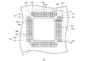
- 矩形状の外形を有する部品底面の対向する二辺のそれぞれに沿って、または前記矩形状の外形の四辺のそれぞれに沿って並ぶ複数の電極パッドを備える表面実装型パッケージ部品と、
前記複数の電極パッドに沿って並ぶ複数のランドを前記部品底面と対向する配線板上面に備え、各ランドが対応する電極パッドと対向して配置され、互いにはんだ接続により電気的に接続されるプリント配線板と、を備え、
前記複数のランドの各ランドと当該ランドに対応する電極パッドとの間に、外側はんだ傾斜面および内側はんだ傾斜面が形成され、
前記複数の電極パッドのうち前記部品底面の辺の端に位置する末端パッドと前記複数のランドのうち前記末端パッドに対応する末端ランドについては、前記外側はんだ傾斜面および前記内側はんだ傾斜面の一方が配線板側を向くとともに他方が部品側を向くように、前記末端ランドが前記末端パッドに対してずれて配置され、
前記末端パッド以外の中央パッドと前記中央パッドに対応する中央ランドについては、前記外側はんだ傾斜面および前記内側はんだ傾斜面がともに部品側を向くように、前記中央ランドが前記対応する中央パッドに対してずれて配置されていることを特徴とする車載用電子回路実装基板。 - 前記末端ランドは、前記末端パッドに対して部品外側にずれて配置され、
前記末端ランドの寸法が、前記末端パッドが設けられた前記部品底面の辺に垂直な方向について、前記末端パッドの寸法より長いことを特徴とする請求項1に記載の車載用電子回路実装基板。 - 前記二辺または前記四辺のそれぞれについて、前記末端ランドと前記末端パッドとの間に、外側はんだ傾斜面および内側はんだ傾斜面が形成され、前記外側はんだ傾斜面および前記内側はんだ傾斜面の一方が配線板側を向くとともに他方が部品側を向くように、前記末端ランドが前記末端パッドに対してずれて配置されていることを特徴とする請求項1または2に記載の車載用電子回路実装基板。
Priority Applications (5)
| Application Number | Priority Date | Filing Date | Title |
|---|---|---|---|
| JP2017139852A JP6956552B2 (ja) | 2017-07-19 | 2017-07-19 | 車載用電子回路実装基板 |
| US16/029,862 US10517177B2 (en) | 2017-07-19 | 2018-07-09 | On-vehicle electronic circuit mounting board |
| CN201810752246.2A CN109287061A (zh) | 2017-07-19 | 2018-07-10 | 车载用电路安装基板 |
| CN201821087826.6U CN209046917U (zh) | 2017-07-19 | 2018-07-10 | 车载用电路安装基板 |
| KR1020180082369A KR102134328B1 (ko) | 2017-07-19 | 2018-07-16 | 차재용 전자 회로 실장 기판 |
Applications Claiming Priority (1)
| Application Number | Priority Date | Filing Date | Title |
|---|---|---|---|
| JP2017139852A JP6956552B2 (ja) | 2017-07-19 | 2017-07-19 | 車載用電子回路実装基板 |
Publications (2)
| Publication Number | Publication Date |
|---|---|
| JP2019021799A JP2019021799A (ja) | 2019-02-07 |
| JP6956552B2 true JP6956552B2 (ja) | 2021-11-02 |
Family
ID=65023582
Family Applications (1)
| Application Number | Title | Priority Date | Filing Date |
|---|---|---|---|
| JP2017139852A Active JP6956552B2 (ja) | 2017-07-19 | 2017-07-19 | 車載用電子回路実装基板 |
Country Status (4)
| Country | Link |
|---|---|
| US (1) | US10517177B2 (ja) |
| JP (1) | JP6956552B2 (ja) |
| KR (1) | KR102134328B1 (ja) |
| CN (2) | CN209046917U (ja) |
Families Citing this family (4)
| Publication number | Priority date | Publication date | Assignee | Title |
|---|---|---|---|---|
| JP6956552B2 (ja) * | 2017-07-19 | 2021-11-02 | 株式会社小糸製作所 | 車載用電子回路実装基板 |
| JP7167721B2 (ja) * | 2019-01-10 | 2022-11-09 | 株式会社デンソー | 半導体装置およびその製造方法 |
| JP7352377B2 (ja) | 2019-05-15 | 2023-09-28 | 株式会社小糸製作所 | 電子部品実装基板およびその製造方法 |
| JP2025031250A (ja) * | 2023-08-25 | 2025-03-07 | 株式会社日立製作所 | 制御基板及びその製造方法 |
Family Cites Families (20)
| Publication number | Priority date | Publication date | Assignee | Title |
|---|---|---|---|---|
| DE4135007C2 (de) * | 1990-10-25 | 1994-12-22 | Cts Corp | SMD-Bauelemente mit Maßnahmen gegen Lötbrückenbildung und Temperaturwechselbeanspruchung |
| JPH09237962A (ja) * | 1995-12-28 | 1997-09-09 | Sanyo Electric Co Ltd | 電子回路装置 |
| JPH1117319A (ja) * | 1997-06-26 | 1999-01-22 | Matsushita Electric Ind Co Ltd | チップの実装方法 |
| JP3645136B2 (ja) * | 1999-06-22 | 2005-05-11 | 三菱電機株式会社 | 電子回路パッケージ及び実装ボード |
| JP3613167B2 (ja) * | 2000-10-12 | 2005-01-26 | 株式会社村田製作所 | パッド電極の接続状態の検査方法 |
| US7506438B1 (en) * | 2000-11-14 | 2009-03-24 | Freescale Semiconductor, Inc. | Low profile integrated module interconnects and method of fabrication |
| JP2004363394A (ja) * | 2003-06-05 | 2004-12-24 | Sony Corp | プリント回路板及びその製造方法、クリームはんだマスク |
| JP4618298B2 (ja) * | 2005-03-29 | 2011-01-26 | 株式会社村田製作所 | 電子部品の実装構造 |
| JP2008227183A (ja) * | 2007-03-13 | 2008-09-25 | Fujitsu Ltd | プリント基板ユニットおよびプリント配線板 |
| JP2008235551A (ja) * | 2007-03-20 | 2008-10-02 | Kyocera Corp | 回路基板およびこれを用いた電子装置 |
| JP2009049258A (ja) * | 2007-08-22 | 2009-03-05 | Nippon Dempa Kogyo Co Ltd | 電子部品の実装方法 |
| US8309864B2 (en) | 2008-01-31 | 2012-11-13 | Sanyo Electric Co., Ltd. | Device mounting board and manufacturing method therefor, and semiconductor module |
| JP2010278133A (ja) * | 2009-05-27 | 2010-12-09 | Murata Mfg Co Ltd | 回路基板 |
| JP2012049219A (ja) * | 2010-08-25 | 2012-03-08 | Fujitsu Ltd | 電子装置 |
| JP5704177B2 (ja) | 2011-01-25 | 2015-04-22 | 株式会社村田製作所 | 電子部品 |
| JP5734434B2 (ja) * | 2011-07-25 | 2015-06-17 | 京セラ株式会社 | 配線基板、電子装置および電子モジュール |
| JP6379542B2 (ja) * | 2014-03-14 | 2018-08-29 | 日亜化学工業株式会社 | 照明装置 |
| JP2017069333A (ja) * | 2015-09-29 | 2017-04-06 | ファナック株式会社 | プリント基板 |
| JP6261625B2 (ja) * | 2016-01-14 | 2018-01-17 | 三菱電機株式会社 | 電子回路装置 |
| JP6956552B2 (ja) * | 2017-07-19 | 2021-11-02 | 株式会社小糸製作所 | 車載用電子回路実装基板 |
-
2017
- 2017-07-19 JP JP2017139852A patent/JP6956552B2/ja active Active
-
2018
- 2018-07-09 US US16/029,862 patent/US10517177B2/en not_active Expired - Fee Related
- 2018-07-10 CN CN201821087826.6U patent/CN209046917U/zh active Active
- 2018-07-10 CN CN201810752246.2A patent/CN109287061A/zh active Pending
- 2018-07-16 KR KR1020180082369A patent/KR102134328B1/ko not_active Expired - Fee Related
Also Published As
| Publication number | Publication date |
|---|---|
| KR20190009710A (ko) | 2019-01-29 |
| CN109287061A (zh) | 2019-01-29 |
| US20190029115A1 (en) | 2019-01-24 |
| JP2019021799A (ja) | 2019-02-07 |
| CN209046917U (zh) | 2019-06-28 |
| US10517177B2 (en) | 2019-12-24 |
| KR102134328B1 (ko) | 2020-07-16 |
Similar Documents
| Publication | Publication Date | Title |
|---|---|---|
| JP6956552B2 (ja) | 車載用電子回路実装基板 | |
| CN102231944A (zh) | 焊点应力削减结构以及包括所述结构的印刷电路板 | |
| JP2016213308A (ja) | プリント回路板及びプリント配線板 | |
| US9059162B2 (en) | Chip on film (COF) substrate, COF package and display device including the same | |
| JP2017175018A (ja) | 半導体装置 | |
| JP2012015469A (ja) | 半導体装置用テープキャリア | |
| US11096285B2 (en) | Electronic circuit substrate | |
| JP4639245B2 (ja) | 半導体素子とそれを用いた半導体装置 | |
| JP2014107541A (ja) | 回路基板及び電子部品を回路基板に実装する方法 | |
| WO2016031440A1 (ja) | チップ抵抗器およびその実装構造 | |
| US12087675B2 (en) | Semiconductor device and mounting structure thereof | |
| US20170150596A1 (en) | Stress reduction interposer for ceramic no-lead surface mount electronic device | |
| CN106206519B (zh) | 包括用于抑制焊桥的电气图案的电气装置 | |
| CN104637906A (zh) | 用于电路基板和半导体封装的焊料桥接阻止结构 | |
| JP6565167B2 (ja) | 実装構造体 | |
| CN111343783A (zh) | 印刷基板 | |
| JP5879090B2 (ja) | プリント配線板 | |
| JP7798556B2 (ja) | 実装基板 | |
| US20100032191A1 (en) | Flexible printed circuitboard structure | |
| JP6487286B2 (ja) | 配線基板 | |
| JP7459610B2 (ja) | 電子装置 | |
| JP7425587B2 (ja) | 電子制御装置 | |
| CN210200722U (zh) | 电子模块用基板 | |
| JP2006294932A (ja) | 回路実装基板のランドおよび表面実装部品が搭載された回路実装基板 | |
| JP2014192298A (ja) | 半導体装置 |
Legal Events
| Date | Code | Title | Description |
|---|---|---|---|
| A621 | Written request for application examination |
Free format text: JAPANESE INTERMEDIATE CODE: A621 Effective date: 20200611 |
|
| A977 | Report on retrieval |
Free format text: JAPANESE INTERMEDIATE CODE: A971007 Effective date: 20210322 |
|
| A131 | Notification of reasons for refusal |
Free format text: JAPANESE INTERMEDIATE CODE: A131 Effective date: 20210330 |
|
| A521 | Written amendment |
Free format text: JAPANESE INTERMEDIATE CODE: A523 Effective date: 20210525 |
|
| TRDD | Decision of grant or rejection written | ||
| A01 | Written decision to grant a patent or to grant a registration (utility model) |
Free format text: JAPANESE INTERMEDIATE CODE: A01 Effective date: 20210921 |
|
| A61 | First payment of annual fees (during grant procedure) |
Free format text: JAPANESE INTERMEDIATE CODE: A61 Effective date: 20211005 |
|
| R150 | Certificate of patent or registration of utility model |
Ref document number: 6956552 Country of ref document: JP Free format text: JAPANESE INTERMEDIATE CODE: R150 |