JP6817895B2 - 半導体装置 - Google Patents
半導体装置 Download PDFInfo
- Publication number
- JP6817895B2 JP6817895B2 JP2017102560A JP2017102560A JP6817895B2 JP 6817895 B2 JP6817895 B2 JP 6817895B2 JP 2017102560 A JP2017102560 A JP 2017102560A JP 2017102560 A JP2017102560 A JP 2017102560A JP 6817895 B2 JP6817895 B2 JP 6817895B2
- Authority
- JP
- Japan
- Prior art keywords
- insulating film
- semiconductor region
- semiconductor
- film
- region
- Prior art date
- Legal status (The legal status is an assumption and is not a legal conclusion. Google has not performed a legal analysis and makes no representation as to the accuracy of the status listed.)
- Active
Links
Images


Classifications
-
- H—ELECTRICITY
- H10—SEMICONDUCTOR DEVICES; ELECTRIC SOLID-STATE DEVICES NOT OTHERWISE PROVIDED FOR
- H10D—INORGANIC ELECTRIC SEMICONDUCTOR DEVICES
- H10D62/00—Semiconductor bodies, or regions thereof, of devices having potential barriers
- H10D62/10—Shapes, relative sizes or dispositions of the regions of the semiconductor bodies; Shapes of the semiconductor bodies
- H10D62/102—Constructional design considerations for preventing surface leakage or controlling electric field concentration
- H10D62/103—Constructional design considerations for preventing surface leakage or controlling electric field concentration for increasing or controlling the breakdown voltage of reverse-biased devices
- H10D62/105—Constructional design considerations for preventing surface leakage or controlling electric field concentration for increasing or controlling the breakdown voltage of reverse-biased devices by having particular doping profiles, shapes or arrangements of PN junctions; by having supplementary regions, e.g. junction termination extension [JTE]
- H10D62/109—Reduced surface field [RESURF] PN junction structures
- H10D62/111—Multiple RESURF structures, e.g. double RESURF or 3D-RESURF structures
-
- H—ELECTRICITY
- H10—SEMICONDUCTOR DEVICES; ELECTRIC SOLID-STATE DEVICES NOT OTHERWISE PROVIDED FOR
- H10W—GENERIC PACKAGES, INTERCONNECTIONS, CONNECTORS OR OTHER CONSTRUCTIONAL DETAILS OF DEVICES COVERED BY CLASS H10
- H10W10/00—Isolation regions in semiconductor bodies between components of integrated devices
- H10W10/01—Manufacture or treatment
- H10W10/011—Manufacture or treatment of isolation regions comprising dielectric materials
- H10W10/014—Manufacture or treatment of isolation regions comprising dielectric materials using trench refilling with dielectric materials, e.g. shallow trench isolations
-
- H—ELECTRICITY
- H10—SEMICONDUCTOR DEVICES; ELECTRIC SOLID-STATE DEVICES NOT OTHERWISE PROVIDED FOR
- H10D—INORGANIC ELECTRIC SEMICONDUCTOR DEVICES
- H10D30/00—Field-effect transistors [FET]
- H10D30/01—Manufacture or treatment
- H10D30/021—Manufacture or treatment of FETs having insulated gates [IGFET]
- H10D30/023—Manufacture or treatment of FETs having insulated gates [IGFET] having multiple independently-addressable gate electrodes influencing the same channel
-
- H—ELECTRICITY
- H10—SEMICONDUCTOR DEVICES; ELECTRIC SOLID-STATE DEVICES NOT OTHERWISE PROVIDED FOR
- H10D—INORGANIC ELECTRIC SEMICONDUCTOR DEVICES
- H10D30/00—Field-effect transistors [FET]
- H10D30/01—Manufacture or treatment
- H10D30/021—Manufacture or treatment of FETs having insulated gates [IGFET]
- H10D30/025—Manufacture or treatment of FETs having insulated gates [IGFET] of vertical IGFETs
-
- H—ELECTRICITY
- H10—SEMICONDUCTOR DEVICES; ELECTRIC SOLID-STATE DEVICES NOT OTHERWISE PROVIDED FOR
- H10D—INORGANIC ELECTRIC SEMICONDUCTOR DEVICES
- H10D30/00—Field-effect transistors [FET]
- H10D30/01—Manufacture or treatment
- H10D30/021—Manufacture or treatment of FETs having insulated gates [IGFET]
- H10D30/028—Manufacture or treatment of FETs having insulated gates [IGFET] of double-diffused metal oxide semiconductor [DMOS] FETs
- H10D30/0291—Manufacture or treatment of FETs having insulated gates [IGFET] of double-diffused metal oxide semiconductor [DMOS] FETs of vertical DMOS [VDMOS] FETs
- H10D30/0297—Manufacture or treatment of FETs having insulated gates [IGFET] of double-diffused metal oxide semiconductor [DMOS] FETs of vertical DMOS [VDMOS] FETs using recessing of the gate electrodes, e.g. to form trench gate electrodes
-
- H—ELECTRICITY
- H10—SEMICONDUCTOR DEVICES; ELECTRIC SOLID-STATE DEVICES NOT OTHERWISE PROVIDED FOR
- H10D—INORGANIC ELECTRIC SEMICONDUCTOR DEVICES
- H10D30/00—Field-effect transistors [FET]
- H10D30/60—Insulated-gate field-effect transistors [IGFET]
- H10D30/611—Insulated-gate field-effect transistors [IGFET] having multiple independently-addressable gate electrodes influencing the same channel
-
- H—ELECTRICITY
- H10—SEMICONDUCTOR DEVICES; ELECTRIC SOLID-STATE DEVICES NOT OTHERWISE PROVIDED FOR
- H10D—INORGANIC ELECTRIC SEMICONDUCTOR DEVICES
- H10D30/00—Field-effect transistors [FET]
- H10D30/60—Insulated-gate field-effect transistors [IGFET]
- H10D30/63—Vertical IGFETs
-
- H—ELECTRICITY
- H10—SEMICONDUCTOR DEVICES; ELECTRIC SOLID-STATE DEVICES NOT OTHERWISE PROVIDED FOR
- H10D—INORGANIC ELECTRIC SEMICONDUCTOR DEVICES
- H10D30/00—Field-effect transistors [FET]
- H10D30/60—Insulated-gate field-effect transistors [IGFET]
- H10D30/64—Double-diffused metal-oxide semiconductor [DMOS] FETs
- H10D30/66—Vertical DMOS [VDMOS] FETs
- H10D30/668—Vertical DMOS [VDMOS] FETs having trench gate electrodes, e.g. UMOS transistors
-
- H—ELECTRICITY
- H10—SEMICONDUCTOR DEVICES; ELECTRIC SOLID-STATE DEVICES NOT OTHERWISE PROVIDED FOR
- H10D—INORGANIC ELECTRIC SEMICONDUCTOR DEVICES
- H10D62/00—Semiconductor bodies, or regions thereof, of devices having potential barriers
- H10D62/10—Shapes, relative sizes or dispositions of the regions of the semiconductor bodies; Shapes of the semiconductor bodies
- H10D62/113—Isolations within a component, i.e. internal isolations
- H10D62/115—Dielectric isolations, e.g. air gaps
- H10D62/116—Dielectric isolations, e.g. air gaps adjoining the input or output regions of field-effect devices, e.g. adjoining source or drain regions
-
- H—ELECTRICITY
- H10—SEMICONDUCTOR DEVICES; ELECTRIC SOLID-STATE DEVICES NOT OTHERWISE PROVIDED FOR
- H10D—INORGANIC ELECTRIC SEMICONDUCTOR DEVICES
- H10D62/00—Semiconductor bodies, or regions thereof, of devices having potential barriers
- H10D62/10—Shapes, relative sizes or dispositions of the regions of the semiconductor bodies; Shapes of the semiconductor bodies
- H10D62/124—Shapes, relative sizes or dispositions of the regions of semiconductor bodies or of junctions between the regions
- H10D62/126—Top-view geometrical layouts of the regions or the junctions
- H10D62/127—Top-view geometrical layouts of the regions or the junctions of cellular field-effect devices, e.g. multicellular DMOS transistors or IGBTs
-
- H—ELECTRICITY
- H10—SEMICONDUCTOR DEVICES; ELECTRIC SOLID-STATE DEVICES NOT OTHERWISE PROVIDED FOR
- H10D—INORGANIC ELECTRIC SEMICONDUCTOR DEVICES
- H10D62/00—Semiconductor bodies, or regions thereof, of devices having potential barriers
- H10D62/10—Shapes, relative sizes or dispositions of the regions of the semiconductor bodies; Shapes of the semiconductor bodies
- H10D62/13—Semiconductor regions connected to electrodes carrying current to be rectified, amplified or switched, e.g. source or drain regions
- H10D62/149—Source or drain regions of field-effect devices
- H10D62/151—Source or drain regions of field-effect devices of IGFETs
- H10D62/156—Drain regions of DMOS transistors
- H10D62/157—Impurity concentrations or distributions
-
- H—ELECTRICITY
- H10—SEMICONDUCTOR DEVICES; ELECTRIC SOLID-STATE DEVICES NOT OTHERWISE PROVIDED FOR
- H10D—INORGANIC ELECTRIC SEMICONDUCTOR DEVICES
- H10D64/00—Electrodes of devices having potential barriers
- H10D64/20—Electrodes characterised by their shapes, relative sizes or dispositions
- H10D64/27—Electrodes not carrying the current to be rectified, amplified, oscillated or switched, e.g. gates
- H10D64/311—Gate electrodes for field-effect devices
- H10D64/411—Gate electrodes for field-effect devices for FETs
- H10D64/511—Gate electrodes for field-effect devices for FETs for IGFETs
- H10D64/512—Disposition of the gate electrodes, e.g. buried gates
- H10D64/513—Disposition of the gate electrodes, e.g. buried gates within recesses in the substrate, e.g. trench gates, groove gates or buried gates
-
- H—ELECTRICITY
- H10—SEMICONDUCTOR DEVICES; ELECTRIC SOLID-STATE DEVICES NOT OTHERWISE PROVIDED FOR
- H10W—GENERIC PACKAGES, INTERCONNECTIONS, CONNECTORS OR OTHER CONSTRUCTIONAL DETAILS OF DEVICES COVERED BY CLASS H10
- H10W10/00—Isolation regions in semiconductor bodies between components of integrated devices
- H10W10/10—Isolation regions comprising dielectric materials
- H10W10/17—Isolation regions comprising dielectric materials formed using trench refilling with dielectric materials, e.g. shallow trench isolations
-
- H—ELECTRICITY
- H10—SEMICONDUCTOR DEVICES; ELECTRIC SOLID-STATE DEVICES NOT OTHERWISE PROVIDED FOR
- H10D—INORGANIC ELECTRIC SEMICONDUCTOR DEVICES
- H10D64/00—Electrodes of devices having potential barriers
- H10D64/60—Electrodes characterised by their materials
- H10D64/66—Electrodes having a conductor capacitively coupled to a semiconductor by an insulator, e.g. MIS electrodes
- H10D64/675—Gate sidewall spacers
- H10D64/679—Gate sidewall spacers comprising air gaps
-
- H—ELECTRICITY
- H10—SEMICONDUCTOR DEVICES; ELECTRIC SOLID-STATE DEVICES NOT OTHERWISE PROVIDED FOR
- H10D—INORGANIC ELECTRIC SEMICONDUCTOR DEVICES
- H10D64/00—Electrodes of devices having potential barriers
- H10D64/60—Electrodes characterised by their materials
- H10D64/66—Electrodes having a conductor capacitively coupled to a semiconductor by an insulator, e.g. MIS electrodes
- H10D64/68—Electrodes having a conductor capacitively coupled to a semiconductor by an insulator, e.g. MIS electrodes characterised by the insulator, e.g. by the gate insulator
- H10D64/687—Electrodes having a conductor capacitively coupled to a semiconductor by an insulator, e.g. MIS electrodes characterised by the insulator, e.g. by the gate insulator having cavities, e.g. porous gate dielectrics having gasses therein
Landscapes
- Insulated Gate Type Field-Effect Transistor (AREA)
- Electrodes Of Semiconductors (AREA)
- Chemical & Material Sciences (AREA)
- Composite Materials (AREA)
Description
なお、図面は模式的または概念的なものであり、各部分の厚みと幅との関係、部分間の大きさの比率などは、必ずしも現実のものと同一とは限らない。また、同じ部分を表す場合であっても、図面により互いの寸法や比率が異なって表される場合もある。
なお、本願明細書と各図において、既出の図に関して前述したものと同様の要素には同一の符号を付して詳細な説明は適宜省略する。
なお、以下で説明する各実施形態について、各半導体領域のp形とn形を反転させて各実施形態を実施しても良い。
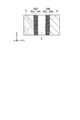
図1は、本実施形態に係る半導体装置を示す斜視図である。
図2は、本実施形態に係る半導体装置を示す断面図である。
図3(a)及び図3(b)は、図2の領域A及び領域Bの拡大図である。
図1及び図2は、半導体装置100の斜視図及び断面図をそれぞれ示している。図2は、図1の半導体装置100の一部を拡大して示している。なお、図1において、ソース電極11及び柱状部60の図示が省略されている。
半導体装置100は、例えば、MOSFETである。
ドレイン領域1の導電形は、例えばn+形である。
半導体領域3は、半導体領域2上に複数設けられ、その導電形は、例えばn形である。半導体領域3は、例えば、nピラー領域である。複数の半導体領域3は、半導体領域2上に選択的に位置する。複数の半導体領域3は、X方向に延びており、Y方向に互いに離間して配置されている。
複数のゲート電極8は、X方向に延びており、Y方向で隣り合う半導体領域5の間に位置するようにY方向に互いに離間して配置されている。また、複数のゲート電極8は、Y方向で隣り合う半導体領域6の間に位置するようにY方向に互いに離間して配置されている。つまり、コンタクト領域7及びゲート電極8は、半導体領域6を介してY方向に交互に配置されている。
ゲート電極8は、例えば、n形不純物を含有した多結晶シリコンを含む。
ドレイン電極10は、ドレイン領域1の下面1b上に設けられている。ドレイン電極10は、ドレイン領域1に電気的に接続される。ドレイン電極10は、例えば、金属材料によって形成される。
ゲート電極8上、及び、ゲート絶縁膜20上には、層間絶縁膜21が設けられている。例えば、層間絶縁膜21は、膜21a及び膜21bの2層構造を有する。膜21aは、例えばシリコン酸化物を含む。膜21bは、膜21a上に設けられ、例えばBPSG(Boro-phospho silicate glass)を含む。
トレンチT内であって、空隙部V上にはカバー膜35が設けられている。カバー膜35は、例えばBPSGを含む。カバー膜35は、例えば、トレンチTにおけるキャップ膜として機能する。絶縁部30は、カバー膜35と、半導体領域4の一部及び半導体領域5との間に位置する。
絶縁部30及びカバー膜35は、内部に空隙部Vが形成された柱状部60を構成する。
絶縁膜30aは、例えば、シリコン酸化物(SiO)を含む。絶縁膜30bは、引張応力を有する材料、例えば、シリコン窒化物(SiN)を含む。絶縁膜30cは、例えば、シリコン酸化物(SiO)を含む。
絶縁膜30a、絶縁膜30b及び絶縁膜30cの形状は、例えば、底を有する筒状である。また、半導体領域4の形状は、例えば、底を有する筒状である。
絶縁膜30aと絶縁膜30cの合計膜厚は、絶縁膜30bの膜厚の0.5倍以上であって4倍以下である。絶縁膜30aと絶縁膜30cの合計膜厚は、絶縁膜30bの膜厚の1倍以上(または同等以上)であって4倍以下であれば、さらに望ましい。絶縁膜30aと絶縁膜30cが、例えばシリコン酸化物(SiO)を含み、絶縁膜30bが、例えばシリコン窒化物(SiN)を含む場合、絶縁膜30aと絶縁膜30cの合計膜厚は、絶縁膜30bの膜厚の1.8倍程度であることが望ましい。
ソース電極11上には、層間絶縁膜22が設けられている。層間絶縁膜22は、例えば、シリコン酸化物を含む。
図4〜図9は、半導体装置100の製造方法を示す断面図である。
なお、図4〜図9に示された領域は、図2に示された領域の一部に相当する。なお、図4〜図9においては、柱状部60より上の部分、及び、半導体領域2より下の部分は示されていない。
まず、図4に示すように、第1導電形の半導体基板40上に、第1導電形の半導体層41をエピタキシャル成長させる。
n形半導体領域とp形半導体領域とがトレンチを介して交互に設けられたスーパージャンクション構造を有するMOSFETでは、セルのピッチの微細化に伴って高アスペクト比のトレンチが形成され易い。トレンチの内面上及び上部上には、p形半導体領域及びカバー膜がそれぞれ形成され、トレンチの一部(p形半導体領域及びカバー膜で囲まれた部分)には空隙部が形成される場合がある。
本実施形態によれば、信頼性が向上した半導体装置及びその製造方法を提供することができる。
図10は、本実施形態に係る半導体装置を示す斜視図である。
図10は、半導体装置200を示す斜視図である。図10に示された領域は、図1に示された領域に相当する。なお、図10において、ソース電極11及び柱状部60の図示が省略されている。
本実施形態において、半導体領域3及び半導体領域4より上の構成が第1実施形態と異なる。よって、これ以外の構成の詳細な説明は省略する。
半導体領域6は、半導体領域5上に複数設けられている。複数の半導体領域6は、X−Y平面を島状に配置されている。
半導体領域5、半導体領域6及びコンタクト領域7をそれぞれ有する複数の領域50は、X−Y平面を島状に配置されている。
ゲートコンタクト9は、ゲート電極8上に設けられている。
本実施形態の効果は、前述の第1実施形態と同じである。
図11は、本実施形態に係る半導体装置を示す断面図である。
図12は、図11の領域Cの拡大図である。
図11に示すように、半導体装置300には、ドレイン領域1と、半導体領域2と、半導体領域3と、半導体領域4と、半導体領域5と、半導体領域6と、ゲート電極8と、ドレイン電極10と、ソース電極11と、ゲート絶縁膜20と、層間絶縁膜21と、絶縁部30と、カバー膜35と、が設けられている。層間絶縁膜21は、膜21a及び膜21bを有する。
半導体領域3は、半導体領域2上に複数設けられている。複数の半導体領域3は、X方向に延びており、Y方向に互いに離間して配置されている。
半導体領域4は、半導体領域2上に複数設けられている。複数の半導体領域4は、X方向に延びており、Y方向で隣り合う半導体領域3の間に位置するようにY方向に互いに離間して配置されている。
半導体領域6は、半導体領域5上に複数設けられている。複数の半導体領域6は、Y方向に互いに離間して配置されている。
ドレイン電極10は、ドレイン領域1の下面1b上に設けられている。
ソース電極11は、半導体領域5の一部上と、半導体領域6の一部上と、層間絶縁膜21上と、絶縁部30上と、カバー膜35上とに設けられている。
絶縁膜30aは、半導体領域51の側面上、及び、半導体領域52の側面上に位置する。また、絶縁膜30aは、トレンチT1の底面上であって半導体領域2上に位置する。
絶縁膜30bは、絶縁膜30aの側面上及び底面上に位置する。
絶縁膜30cは、絶縁膜30bの側面上及び底面上に位置する。
つまり、絶縁部30は、カバー膜35の側面と、空隙部Vの側面及び底面とを覆っており、絶縁膜30c、30b、30aがこれらの側面及び底面から離れる方向にこの順で位置する。絶縁膜30a、絶縁膜30b及び絶縁膜30cの形状は、例えば、底を有する筒状である。
本実施形態の効果は、前述の第1実施形態と同じである。
Claims (4)
- 第1方向に延びる第1導電形の第1半導体領域と、
前記第1方向に延び、前記第1方向に交差する第2方向に前記第1半導体領域と配置され、空隙を囲む第2導電形の第2半導体領域と、
前記空隙と、前記第2半導体領域との間に設けられ、シリコン酸化物を含む第1絶縁膜と、シリコン窒化物を含む第2絶縁膜と、シリコン酸化物を含む第3絶縁膜とを有する絶縁部と、
を備え、
前記第1絶縁膜、前記第2絶縁膜及び前記第3絶縁膜は、前記第2半導体領域から前記空隙に向かって順に位置し、
前記第1絶縁膜と前記第3絶縁膜の厚さの合計は、前記第2絶縁膜の厚さの0.5倍以上であって4倍以下である半導体装置。 - 前記第1絶縁膜は、前記第2半導体領域の側面上及び底面上に位置し、
前記第2絶縁膜は、前記第1絶縁膜の側面上及び底面上に位置し、
前記第3絶縁膜は、前記第2絶縁膜の側面上及び底面上に位置する請求項1記載の半導体装置。 - 前記第1半導体領域及び前記第2半導体領域上に設けられた第2導電形の第3半導体領域と、
前記空隙上に設けられ、前記第3半導体領域との間で前記絶縁部が位置するカバー膜と、
をさらに備えた請求項1または2に記載の半導体装置。 - 第1方向に延びる第1導電形の第1半導体領域と、
前記第1方向に延び、前記第1方向に交差する第2方向に空隙を介して前記第1半導体領域と配置される第2導電形の第2半導体領域と、
前記空隙と、前記第1半導体領域及び前記第2半導体領域との間に設けられ、シリコン酸化物を含む第1絶縁膜と、シリコン窒化物を含む第2絶縁膜と、シリコン酸化物を含む第3絶縁膜とを有する絶縁部と、
を備えた半導体装置。
Priority Applications (3)
| Application Number | Priority Date | Filing Date | Title |
|---|---|---|---|
| JP2017102560A JP6817895B2 (ja) | 2017-05-24 | 2017-05-24 | 半導体装置 |
| CN201710790536.1A CN108962993B (zh) | 2017-05-24 | 2017-09-05 | 半导体装置及其制造方法 |
| US15/876,412 US10431491B2 (en) | 2017-05-24 | 2018-01-22 | Semiconductor device having a triple insulating film surrounded void |
Applications Claiming Priority (1)
| Application Number | Priority Date | Filing Date | Title |
|---|---|---|---|
| JP2017102560A JP6817895B2 (ja) | 2017-05-24 | 2017-05-24 | 半導体装置 |
Publications (3)
| Publication Number | Publication Date |
|---|---|
| JP2018198267A JP2018198267A (ja) | 2018-12-13 |
| JP2018198267A5 JP2018198267A5 (ja) | 2019-10-03 |
| JP6817895B2 true JP6817895B2 (ja) | 2021-01-20 |
Family
ID=64401126
Family Applications (1)
| Application Number | Title | Priority Date | Filing Date |
|---|---|---|---|
| JP2017102560A Active JP6817895B2 (ja) | 2017-05-24 | 2017-05-24 | 半導体装置 |
Country Status (3)
| Country | Link |
|---|---|
| US (1) | US10431491B2 (ja) |
| JP (1) | JP6817895B2 (ja) |
| CN (1) | CN108962993B (ja) |
Families Citing this family (7)
| Publication number | Priority date | Publication date | Assignee | Title |
|---|---|---|---|---|
| US10903331B2 (en) * | 2019-03-25 | 2021-01-26 | International Business Machines Corporation | Positioning air-gap spacers in a transistor for improved control of parasitic capacitance |
| JP7317752B2 (ja) | 2020-03-17 | 2023-07-31 | 株式会社東芝 | 半導体装置 |
| JP7490597B2 (ja) * | 2021-03-05 | 2024-05-27 | 株式会社東芝 | 半導体装置およびその製造方法 |
| US20230051830A1 (en) * | 2021-08-13 | 2023-02-16 | Infineon Technologies Ag | Semiconductor device and method of producing thereof |
| DE102021121138B3 (de) * | 2021-08-13 | 2023-02-02 | Infineon Technologies Ag | Halbleitervorrichtungen und verfahren zum herstellen einer halbleitervorrichtung |
| CN115775823B (zh) * | 2022-11-29 | 2023-07-21 | 上海功成半导体科技有限公司 | 屏蔽栅功率器件及其制备方法 |
| EP4411822A1 (en) * | 2023-02-02 | 2024-08-07 | Infineon Technologies Austria AG | Semiconductor device and method of fabricating an electrically insulating structure in a trench |
Family Cites Families (34)
| Publication number | Priority date | Publication date | Assignee | Title |
|---|---|---|---|---|
| US5937296A (en) * | 1996-12-20 | 1999-08-10 | Siemens Aktiengesellschaft | Memory cell that includes a vertical transistor and a trench capacitor |
| DE19748523C2 (de) | 1997-11-03 | 1999-10-07 | Siemens Ag | Halbleiterbauelement, Verfahren zum Herstellen eines derartigen Halbleiterbauelementes und Verwendung des Verfahrens |
| US6337499B1 (en) * | 1997-11-03 | 2002-01-08 | Infineon Technologies Ag | Semiconductor component |
| JP2000196074A (ja) * | 1998-12-25 | 2000-07-14 | Toshiba Corp | 半導体装置およびその製造方法 |
| FR2795554B1 (fr) * | 1999-06-28 | 2003-08-22 | France Telecom | Procede de gravure laterale par trous pour fabriquer des dis positifs semi-conducteurs |
| JP4285899B2 (ja) | 2000-10-10 | 2009-06-24 | 三菱電機株式会社 | 溝を有する半導体装置 |
| US6521954B1 (en) * | 2001-12-21 | 2003-02-18 | Kabushiki Kaisha Toshiba | Semiconductor device and manufacturing method thereof |
| JP3993458B2 (ja) * | 2002-04-17 | 2007-10-17 | 株式会社東芝 | 半導体装置 |
| JP3634848B2 (ja) * | 2003-01-07 | 2005-03-30 | 株式会社東芝 | 電力用半導体素子 |
| JP2006066611A (ja) * | 2004-08-26 | 2006-03-09 | Toshiba Corp | 半導体装置 |
| JP4830285B2 (ja) * | 2004-11-08 | 2011-12-07 | 株式会社デンソー | 炭化珪素半導体装置の製造方法 |
| JP5011881B2 (ja) * | 2006-08-11 | 2012-08-29 | 株式会社デンソー | 半導体装置の製造方法 |
| JP2008210940A (ja) * | 2007-02-26 | 2008-09-11 | Elpida Memory Inc | 半導体装置及びその製造方法 |
| JP5583315B2 (ja) * | 2007-07-19 | 2014-09-03 | ピーエスフォー ルクスコ エスエイアールエル | 半導体装置及びその製造方法 |
| JP4973418B2 (ja) * | 2007-09-26 | 2012-07-11 | サンケン電気株式会社 | 半導体装置 |
| US7956411B2 (en) * | 2008-01-15 | 2011-06-07 | Fairchild Semiconductor Corporation | High aspect ratio trench structures with void-free fill material |
| US7960781B2 (en) * | 2008-09-08 | 2011-06-14 | Semiconductor Components Industries, Llc | Semiconductor device having vertical charge-compensated structure and sub-surface connecting layer and method |
| JP5400405B2 (ja) * | 2009-02-05 | 2014-01-29 | 株式会社東芝 | 半導体装置の製造方法 |
| US8319278B1 (en) * | 2009-03-31 | 2012-11-27 | Maxpower Semiconductor, Inc. | Power device structures and methods using empty space zones |
| KR101802220B1 (ko) * | 2010-12-20 | 2017-11-29 | 삼성전자주식회사 | 수직형 채널 트랜지스터를 포함하는 반도체 소자 및 그 제조 방법 |
| WO2013001677A1 (ja) * | 2011-06-28 | 2013-01-03 | パナソニック株式会社 | 半導体装置とその製造方法 |
| US8907408B2 (en) * | 2012-03-26 | 2014-12-09 | Infineon Technologies Austria Ag | Stress-reduced field-effect semiconductor device and method for forming therefor |
| US9024383B2 (en) * | 2013-05-01 | 2015-05-05 | Infineon Technologies Austria Ag | Semiconductor device with a super junction structure with one, two or more pairs of compensation layers |
| US9070580B2 (en) * | 2013-05-01 | 2015-06-30 | Infineon Technologies Austria Ag | Semiconductor device with a super junction structure based on a compensation structure with compensation layers and having a compensation rate gradient |
| KR102078852B1 (ko) * | 2013-08-29 | 2020-02-18 | 삼성전자 주식회사 | 반도체 장치 및 그 제조 방법 |
| US9560765B2 (en) * | 2013-12-06 | 2017-01-31 | Infineon Technologies Dresden Gmbh | Electronic device, a method for manufacturing an electronic device, and a method for operating an electronic device |
| US9953861B2 (en) * | 2014-11-26 | 2018-04-24 | Taiwan Semiconductor Manufacturing Company, Ltd. | Semiconductor device having a shallow trench isolation structure and methods of forming the same |
| US9666507B2 (en) * | 2014-11-30 | 2017-05-30 | United Microelectronics Corp. | Through-substrate structure and method for fabricating the same |
| JP2016139676A (ja) * | 2015-01-27 | 2016-08-04 | トヨタ自動車株式会社 | 半導体装置と、その製造方法 |
| US9379043B1 (en) * | 2015-02-10 | 2016-06-28 | Powertech Technology Inc. | TSV structure having insulating layers with embedded voids |
| JP6509635B2 (ja) * | 2015-05-29 | 2019-05-08 | 東芝メモリ株式会社 | 半導体装置、及び、半導体装置の製造方法 |
| JP6301882B2 (ja) * | 2015-08-21 | 2018-03-28 | トヨタ自動車株式会社 | 半導体装置の製造方法と半導体装置 |
| US9929271B2 (en) * | 2016-08-03 | 2018-03-27 | Taiwan Semiconductor Manufacturing Company, Ltd. | Semiconductor device and method |
| JP2018046251A (ja) * | 2016-09-16 | 2018-03-22 | 株式会社東芝 | 半導体装置およびその製造方法 |
-
2017
- 2017-05-24 JP JP2017102560A patent/JP6817895B2/ja active Active
- 2017-09-05 CN CN201710790536.1A patent/CN108962993B/zh active Active
-
2018
- 2018-01-22 US US15/876,412 patent/US10431491B2/en active Active
Also Published As
| Publication number | Publication date |
|---|---|
| US20180342415A1 (en) | 2018-11-29 |
| CN108962993B (zh) | 2021-09-24 |
| JP2018198267A (ja) | 2018-12-13 |
| US10431491B2 (en) | 2019-10-01 |
| CN108962993A (zh) | 2018-12-07 |
Similar Documents
| Publication | Publication Date | Title |
|---|---|---|
| JP6817895B2 (ja) | 半導体装置 | |
| US10319850B2 (en) | Semiconductor device and manufacturing method of semiconductor device | |
| US20240379839A1 (en) | Semiconductor device | |
| JP6378220B2 (ja) | 半導体装置 | |
| US8269272B2 (en) | Semiconductor device and method for manufacturing the same | |
| JP5298565B2 (ja) | 半導体装置およびその製造方法 | |
| JP6958575B2 (ja) | 半導体装置およびその製造方法 | |
| JP6312933B2 (ja) | 電力用半導体装置 | |
| US20180358445A1 (en) | Semiconductor device and method of manufacturing semiconductor device | |
| JP2018129378A (ja) | 半導体装置および半導体装置の製造方法、ならびに、半導体ウエハ構造物 | |
| JP2017162909A (ja) | 半導体装置 | |
| CN102403356A (zh) | 半导体装置 | |
| JP6193163B2 (ja) | 絶縁ゲート型半導体装置 | |
| JP2013258327A (ja) | 半導体装置及びその製造方法 | |
| TWI590449B (zh) | Silicon carbide semiconductor device, method of manufacturing the silicon carbide semiconductor device, and method of designing the silicon carbide semiconductor device | |
| JP2015050390A (ja) | 半導体装置 | |
| JP2017045776A (ja) | 半導体装置およびその製造方法 | |
| JP2005322700A (ja) | 半導体装置及びその製造方法 | |
| JP2018152522A (ja) | 半導体装置および半導体装置の製造方法 | |
| JP2017188590A (ja) | 半導体装置およびその製造方法 | |
| CN113053752B (zh) | 半导体器件及其制造方法 | |
| JP2015146399A (ja) | 半導体装置及び半導体装置の製造方法 | |
| JP4735235B2 (ja) | 絶縁ゲート型半導体装置およびその製造方法 | |
| TWI574405B (zh) | Silicon carbide semiconductor device, method for manufacturing silicon carbide semiconductor device, and design method of silicon carbide semiconductor device | |
| JP2012160601A (ja) | 半導体装置の製造方法 |
Legal Events
| Date | Code | Title | Description |
|---|---|---|---|
| A711 | Notification of change in applicant |
Free format text: JAPANESE INTERMEDIATE CODE: A712 Effective date: 20171116 |
|
| A711 | Notification of change in applicant |
Free format text: JAPANESE INTERMEDIATE CODE: A711 Effective date: 20171117 |
|
| A521 | Request for written amendment filed |
Free format text: JAPANESE INTERMEDIATE CODE: A523 Effective date: 20190809 |
|
| A621 | Written request for application examination |
Free format text: JAPANESE INTERMEDIATE CODE: A621 Effective date: 20190809 |
|
| A977 | Report on retrieval |
Free format text: JAPANESE INTERMEDIATE CODE: A971007 Effective date: 20200630 |
|
| A131 | Notification of reasons for refusal |
Free format text: JAPANESE INTERMEDIATE CODE: A131 Effective date: 20200730 |
|
| A521 | Request for written amendment filed |
Free format text: JAPANESE INTERMEDIATE CODE: A523 Effective date: 20200916 |
|
| TRDD | Decision of grant or rejection written | ||
| A01 | Written decision to grant a patent or to grant a registration (utility model) |
Free format text: JAPANESE INTERMEDIATE CODE: A01 Effective date: 20201127 |
|
| A61 | First payment of annual fees (during grant procedure) |
Free format text: JAPANESE INTERMEDIATE CODE: A61 Effective date: 20201225 |
|
| R150 | Certificate of patent or registration of utility model |
Ref document number: 6817895 Country of ref document: JP Free format text: JAPANESE INTERMEDIATE CODE: R150 |