JP6817895B2 - Semiconductor device - Google Patents
Semiconductor device Download PDFInfo
- Publication number
- JP6817895B2 JP6817895B2 JP2017102560A JP2017102560A JP6817895B2 JP 6817895 B2 JP6817895 B2 JP 6817895B2 JP 2017102560 A JP2017102560 A JP 2017102560A JP 2017102560 A JP2017102560 A JP 2017102560A JP 6817895 B2 JP6817895 B2 JP 6817895B2
- Authority
- JP
- Japan
- Prior art keywords
- insulating film
- semiconductor region
- semiconductor
- film
- region
- Prior art date
- Legal status (The legal status is an assumption and is not a legal conclusion. Google has not performed a legal analysis and makes no representation as to the accuracy of the status listed.)
- Active
Links
- 239000004065 semiconductor Substances 0.000 title claims description 231
- 239000010408 film Substances 0.000 claims description 189
- 239000013039 cover film Substances 0.000 claims description 37
- VYPSYNLAJGMNEJ-UHFFFAOYSA-N Silicium dioxide Chemical compound O=[Si]=O VYPSYNLAJGMNEJ-UHFFFAOYSA-N 0.000 claims description 14
- 229910052814 silicon oxide Inorganic materials 0.000 claims description 14
- 229910052581 Si3N4 Inorganic materials 0.000 claims description 9
- HQVNEWCFYHHQES-UHFFFAOYSA-N silicon nitride Chemical compound N12[Si]34N5[Si]62N3[Si]51N64 HQVNEWCFYHHQES-UHFFFAOYSA-N 0.000 claims description 9
- 239000011800 void material Substances 0.000 claims description 5
- 238000009413 insulation Methods 0.000 claims 2
- 239000012535 impurity Substances 0.000 description 15
- 238000000034 method Methods 0.000 description 13
- 238000004519 manufacturing process Methods 0.000 description 12
- 239000011229 interlayer Substances 0.000 description 11
- 239000000463 material Substances 0.000 description 9
- 239000010410 layer Substances 0.000 description 8
- 238000005229 chemical vapour deposition Methods 0.000 description 5
- 239000005380 borophosphosilicate glass Substances 0.000 description 4
- LIVNPJMFVYWSIS-UHFFFAOYSA-N silicon monoxide Chemical compound [Si-]#[O+] LIVNPJMFVYWSIS-UHFFFAOYSA-N 0.000 description 4
- 239000000758 substrate Substances 0.000 description 4
- 230000000694 effects Effects 0.000 description 3
- 239000007769 metal material Substances 0.000 description 3
- 238000001020 plasma etching Methods 0.000 description 3
- ZOXJGFHDIHLPTG-UHFFFAOYSA-N Boron Chemical compound [B] ZOXJGFHDIHLPTG-UHFFFAOYSA-N 0.000 description 2
- OAICVXFJPJFONN-UHFFFAOYSA-N Phosphorus Chemical compound [P] OAICVXFJPJFONN-UHFFFAOYSA-N 0.000 description 2
- 229910052796 boron Inorganic materials 0.000 description 2
- 238000005530 etching Methods 0.000 description 2
- 238000001459 lithography Methods 0.000 description 2
- 238000004518 low pressure chemical vapour deposition Methods 0.000 description 2
- 230000003647 oxidation Effects 0.000 description 2
- 238000007254 oxidation reaction Methods 0.000 description 2
- 229910052698 phosphorus Inorganic materials 0.000 description 2
- 239000011574 phosphorus Substances 0.000 description 2
- 239000000126 substance Substances 0.000 description 2
- 238000000137 annealing Methods 0.000 description 1
- 239000011248 coating agent Substances 0.000 description 1
- 238000000576 coating method Methods 0.000 description 1
- 238000000151 deposition Methods 0.000 description 1
- 238000001312 dry etching Methods 0.000 description 1
- 230000005669 field effect Effects 0.000 description 1
- 238000005468 ion implantation Methods 0.000 description 1
- 230000007257 malfunction Effects 0.000 description 1
- 229910044991 metal oxide Inorganic materials 0.000 description 1
- 150000004706 metal oxides Chemical class 0.000 description 1
- 238000012986 modification Methods 0.000 description 1
- 230000004048 modification Effects 0.000 description 1
- 229910021421 monocrystalline silicon Inorganic materials 0.000 description 1
- 230000002093 peripheral effect Effects 0.000 description 1
- 238000005498 polishing Methods 0.000 description 1
- 229910021420 polycrystalline silicon Inorganic materials 0.000 description 1
Images


Classifications
-
- H—ELECTRICITY
- H01—ELECTRIC ELEMENTS
- H01L—SEMICONDUCTOR DEVICES NOT COVERED BY CLASS H10
- H01L21/00—Processes or apparatus adapted for the manufacture or treatment of semiconductor or solid state devices or of parts thereof
- H01L21/70—Manufacture or treatment of devices consisting of a plurality of solid state components formed in or on a common substrate or of parts thereof; Manufacture of integrated circuit devices or of parts thereof
- H01L21/71—Manufacture of specific parts of devices defined in group H01L21/70
- H01L21/76—Making of isolation regions between components
- H01L21/762—Dielectric regions, e.g. EPIC dielectric isolation, LOCOS; Trench refilling techniques, SOI technology, use of channel stoppers
- H01L21/76224—Dielectric regions, e.g. EPIC dielectric isolation, LOCOS; Trench refilling techniques, SOI technology, use of channel stoppers using trench refilling with dielectric materials
-
- H—ELECTRICITY
- H01—ELECTRIC ELEMENTS
- H01L—SEMICONDUCTOR DEVICES NOT COVERED BY CLASS H10
- H01L29/00—Semiconductor devices adapted for rectifying, amplifying, oscillating or switching, or capacitors or resistors with at least one potential-jump barrier or surface barrier, e.g. PN junction depletion layer or carrier concentration layer; Details of semiconductor bodies or of electrodes thereof ; Multistep manufacturing processes therefor
- H01L29/02—Semiconductor bodies ; Multistep manufacturing processes therefor
- H01L29/06—Semiconductor bodies ; Multistep manufacturing processes therefor characterised by their shape; characterised by the shapes, relative sizes, or dispositions of the semiconductor regions ; characterised by the concentration or distribution of impurities within semiconductor regions
- H01L29/0603—Semiconductor bodies ; Multistep manufacturing processes therefor characterised by their shape; characterised by the shapes, relative sizes, or dispositions of the semiconductor regions ; characterised by the concentration or distribution of impurities within semiconductor regions characterised by particular constructional design considerations, e.g. for preventing surface leakage, for controlling electric field concentration or for internal isolations regions
- H01L29/0607—Semiconductor bodies ; Multistep manufacturing processes therefor characterised by their shape; characterised by the shapes, relative sizes, or dispositions of the semiconductor regions ; characterised by the concentration or distribution of impurities within semiconductor regions characterised by particular constructional design considerations, e.g. for preventing surface leakage, for controlling electric field concentration or for internal isolations regions for preventing surface leakage or controlling electric field concentration
- H01L29/0611—Semiconductor bodies ; Multistep manufacturing processes therefor characterised by their shape; characterised by the shapes, relative sizes, or dispositions of the semiconductor regions ; characterised by the concentration or distribution of impurities within semiconductor regions characterised by particular constructional design considerations, e.g. for preventing surface leakage, for controlling electric field concentration or for internal isolations regions for preventing surface leakage or controlling electric field concentration for increasing or controlling the breakdown voltage of reverse biased devices
- H01L29/0615—Semiconductor bodies ; Multistep manufacturing processes therefor characterised by their shape; characterised by the shapes, relative sizes, or dispositions of the semiconductor regions ; characterised by the concentration or distribution of impurities within semiconductor regions characterised by particular constructional design considerations, e.g. for preventing surface leakage, for controlling electric field concentration or for internal isolations regions for preventing surface leakage or controlling electric field concentration for increasing or controlling the breakdown voltage of reverse biased devices by the doping profile or the shape or the arrangement of the PN junction, or with supplementary regions, e.g. junction termination extension [JTE]
- H01L29/063—Reduced surface field [RESURF] pn-junction structures
- H01L29/0634—Multiple reduced surface field (multi-RESURF) structures, e.g. double RESURF, charge compensation, cool, superjunction (SJ), 3D-RESURF, composite buffer (CB) structures
-
- H—ELECTRICITY
- H01—ELECTRIC ELEMENTS
- H01L—SEMICONDUCTOR DEVICES NOT COVERED BY CLASS H10
- H01L29/00—Semiconductor devices adapted for rectifying, amplifying, oscillating or switching, or capacitors or resistors with at least one potential-jump barrier or surface barrier, e.g. PN junction depletion layer or carrier concentration layer; Details of semiconductor bodies or of electrodes thereof ; Multistep manufacturing processes therefor
- H01L29/02—Semiconductor bodies ; Multistep manufacturing processes therefor
- H01L29/06—Semiconductor bodies ; Multistep manufacturing processes therefor characterised by their shape; characterised by the shapes, relative sizes, or dispositions of the semiconductor regions ; characterised by the concentration or distribution of impurities within semiconductor regions
- H01L29/0603—Semiconductor bodies ; Multistep manufacturing processes therefor characterised by their shape; characterised by the shapes, relative sizes, or dispositions of the semiconductor regions ; characterised by the concentration or distribution of impurities within semiconductor regions characterised by particular constructional design considerations, e.g. for preventing surface leakage, for controlling electric field concentration or for internal isolations regions
- H01L29/0642—Isolation within the component, i.e. internal isolation
- H01L29/0649—Dielectric regions, e.g. SiO2 regions, air gaps
- H01L29/0653—Dielectric regions, e.g. SiO2 regions, air gaps adjoining the input or output region of a field-effect device, e.g. the source or drain region
-
- H—ELECTRICITY
- H01—ELECTRIC ELEMENTS
- H01L—SEMICONDUCTOR DEVICES NOT COVERED BY CLASS H10
- H01L29/00—Semiconductor devices adapted for rectifying, amplifying, oscillating or switching, or capacitors or resistors with at least one potential-jump barrier or surface barrier, e.g. PN junction depletion layer or carrier concentration layer; Details of semiconductor bodies or of electrodes thereof ; Multistep manufacturing processes therefor
- H01L29/02—Semiconductor bodies ; Multistep manufacturing processes therefor
- H01L29/06—Semiconductor bodies ; Multistep manufacturing processes therefor characterised by their shape; characterised by the shapes, relative sizes, or dispositions of the semiconductor regions ; characterised by the concentration or distribution of impurities within semiconductor regions
- H01L29/0684—Semiconductor bodies ; Multistep manufacturing processes therefor characterised by their shape; characterised by the shapes, relative sizes, or dispositions of the semiconductor regions ; characterised by the concentration or distribution of impurities within semiconductor regions characterised by the shape, relative sizes or dispositions of the semiconductor regions or junctions between the regions
- H01L29/0692—Surface layout
- H01L29/0696—Surface layout of cellular field-effect devices, e.g. multicellular DMOS transistors or IGBTs
-
- H—ELECTRICITY
- H01—ELECTRIC ELEMENTS
- H01L—SEMICONDUCTOR DEVICES NOT COVERED BY CLASS H10
- H01L29/00—Semiconductor devices adapted for rectifying, amplifying, oscillating or switching, or capacitors or resistors with at least one potential-jump barrier or surface barrier, e.g. PN junction depletion layer or carrier concentration layer; Details of semiconductor bodies or of electrodes thereof ; Multistep manufacturing processes therefor
- H01L29/02—Semiconductor bodies ; Multistep manufacturing processes therefor
- H01L29/06—Semiconductor bodies ; Multistep manufacturing processes therefor characterised by their shape; characterised by the shapes, relative sizes, or dispositions of the semiconductor regions ; characterised by the concentration or distribution of impurities within semiconductor regions
- H01L29/08—Semiconductor bodies ; Multistep manufacturing processes therefor characterised by their shape; characterised by the shapes, relative sizes, or dispositions of the semiconductor regions ; characterised by the concentration or distribution of impurities within semiconductor regions with semiconductor regions connected to an electrode carrying current to be rectified, amplified or switched and such electrode being part of a semiconductor device which comprises three or more electrodes
- H01L29/0843—Source or drain regions of field-effect devices
- H01L29/0847—Source or drain regions of field-effect devices of field-effect transistors with insulated gate
- H01L29/0852—Source or drain regions of field-effect devices of field-effect transistors with insulated gate of DMOS transistors
- H01L29/0873—Drain regions
- H01L29/0878—Impurity concentration or distribution
-
- H—ELECTRICITY
- H01—ELECTRIC ELEMENTS
- H01L—SEMICONDUCTOR DEVICES NOT COVERED BY CLASS H10
- H01L29/00—Semiconductor devices adapted for rectifying, amplifying, oscillating or switching, or capacitors or resistors with at least one potential-jump barrier or surface barrier, e.g. PN junction depletion layer or carrier concentration layer; Details of semiconductor bodies or of electrodes thereof ; Multistep manufacturing processes therefor
- H01L29/40—Electrodes ; Multistep manufacturing processes therefor
- H01L29/41—Electrodes ; Multistep manufacturing processes therefor characterised by their shape, relative sizes or dispositions
- H01L29/423—Electrodes ; Multistep manufacturing processes therefor characterised by their shape, relative sizes or dispositions not carrying the current to be rectified, amplified or switched
- H01L29/42312—Gate electrodes for field effect devices
- H01L29/42316—Gate electrodes for field effect devices for field-effect transistors
- H01L29/4232—Gate electrodes for field effect devices for field-effect transistors with insulated gate
- H01L29/42356—Disposition, e.g. buried gate electrode
- H01L29/4236—Disposition, e.g. buried gate electrode within a trench, e.g. trench gate electrode, groove gate electrode
-
- H—ELECTRICITY
- H01—ELECTRIC ELEMENTS
- H01L—SEMICONDUCTOR DEVICES NOT COVERED BY CLASS H10
- H01L29/00—Semiconductor devices adapted for rectifying, amplifying, oscillating or switching, or capacitors or resistors with at least one potential-jump barrier or surface barrier, e.g. PN junction depletion layer or carrier concentration layer; Details of semiconductor bodies or of electrodes thereof ; Multistep manufacturing processes therefor
- H01L29/66—Types of semiconductor device ; Multistep manufacturing processes therefor
- H01L29/66007—Multistep manufacturing processes
- H01L29/66075—Multistep manufacturing processes of devices having semiconductor bodies comprising group 14 or group 13/15 materials
- H01L29/66227—Multistep manufacturing processes of devices having semiconductor bodies comprising group 14 or group 13/15 materials the devices being controllable only by the electric current supplied or the electric potential applied, to an electrode which does not carry the current to be rectified, amplified or switched, e.g. three-terminal devices
- H01L29/66409—Unipolar field-effect transistors
- H01L29/66477—Unipolar field-effect transistors with an insulated gate, i.e. MISFET
- H01L29/66484—Unipolar field-effect transistors with an insulated gate, i.e. MISFET with multiple gate, at least one gate being an insulated gate
-
- H—ELECTRICITY
- H01—ELECTRIC ELEMENTS
- H01L—SEMICONDUCTOR DEVICES NOT COVERED BY CLASS H10
- H01L29/00—Semiconductor devices adapted for rectifying, amplifying, oscillating or switching, or capacitors or resistors with at least one potential-jump barrier or surface barrier, e.g. PN junction depletion layer or carrier concentration layer; Details of semiconductor bodies or of electrodes thereof ; Multistep manufacturing processes therefor
- H01L29/66—Types of semiconductor device ; Multistep manufacturing processes therefor
- H01L29/66007—Multistep manufacturing processes
- H01L29/66075—Multistep manufacturing processes of devices having semiconductor bodies comprising group 14 or group 13/15 materials
- H01L29/66227—Multistep manufacturing processes of devices having semiconductor bodies comprising group 14 or group 13/15 materials the devices being controllable only by the electric current supplied or the electric potential applied, to an electrode which does not carry the current to be rectified, amplified or switched, e.g. three-terminal devices
- H01L29/66409—Unipolar field-effect transistors
- H01L29/66477—Unipolar field-effect transistors with an insulated gate, i.e. MISFET
- H01L29/66666—Vertical transistors
-
- H—ELECTRICITY
- H01—ELECTRIC ELEMENTS
- H01L—SEMICONDUCTOR DEVICES NOT COVERED BY CLASS H10
- H01L29/00—Semiconductor devices adapted for rectifying, amplifying, oscillating or switching, or capacitors or resistors with at least one potential-jump barrier or surface barrier, e.g. PN junction depletion layer or carrier concentration layer; Details of semiconductor bodies or of electrodes thereof ; Multistep manufacturing processes therefor
- H01L29/66—Types of semiconductor device ; Multistep manufacturing processes therefor
- H01L29/66007—Multistep manufacturing processes
- H01L29/66075—Multistep manufacturing processes of devices having semiconductor bodies comprising group 14 or group 13/15 materials
- H01L29/66227—Multistep manufacturing processes of devices having semiconductor bodies comprising group 14 or group 13/15 materials the devices being controllable only by the electric current supplied or the electric potential applied, to an electrode which does not carry the current to be rectified, amplified or switched, e.g. three-terminal devices
- H01L29/66409—Unipolar field-effect transistors
- H01L29/66477—Unipolar field-effect transistors with an insulated gate, i.e. MISFET
- H01L29/66674—DMOS transistors, i.e. MISFETs with a channel accommodating body or base region adjoining a drain drift region
- H01L29/66712—Vertical DMOS transistors, i.e. VDMOS transistors
- H01L29/66734—Vertical DMOS transistors, i.e. VDMOS transistors with a step of recessing the gate electrode, e.g. to form a trench gate electrode
-
- H—ELECTRICITY
- H01—ELECTRIC ELEMENTS
- H01L—SEMICONDUCTOR DEVICES NOT COVERED BY CLASS H10
- H01L29/00—Semiconductor devices adapted for rectifying, amplifying, oscillating or switching, or capacitors or resistors with at least one potential-jump barrier or surface barrier, e.g. PN junction depletion layer or carrier concentration layer; Details of semiconductor bodies or of electrodes thereof ; Multistep manufacturing processes therefor
- H01L29/66—Types of semiconductor device ; Multistep manufacturing processes therefor
- H01L29/68—Types of semiconductor device ; Multistep manufacturing processes therefor controllable by only the electric current supplied, or only the electric potential applied, to an electrode which does not carry the current to be rectified, amplified or switched
- H01L29/76—Unipolar devices, e.g. field effect transistors
- H01L29/772—Field effect transistors
- H01L29/78—Field effect transistors with field effect produced by an insulated gate
- H01L29/7801—DMOS transistors, i.e. MISFETs with a channel accommodating body or base region adjoining a drain drift region
- H01L29/7802—Vertical DMOS transistors, i.e. VDMOS transistors
- H01L29/7813—Vertical DMOS transistors, i.e. VDMOS transistors with trench gate electrode, e.g. UMOS transistors
-
- H—ELECTRICITY
- H01—ELECTRIC ELEMENTS
- H01L—SEMICONDUCTOR DEVICES NOT COVERED BY CLASS H10
- H01L29/00—Semiconductor devices adapted for rectifying, amplifying, oscillating or switching, or capacitors or resistors with at least one potential-jump barrier or surface barrier, e.g. PN junction depletion layer or carrier concentration layer; Details of semiconductor bodies or of electrodes thereof ; Multistep manufacturing processes therefor
- H01L29/66—Types of semiconductor device ; Multistep manufacturing processes therefor
- H01L29/68—Types of semiconductor device ; Multistep manufacturing processes therefor controllable by only the electric current supplied, or only the electric potential applied, to an electrode which does not carry the current to be rectified, amplified or switched
- H01L29/76—Unipolar devices, e.g. field effect transistors
- H01L29/772—Field effect transistors
- H01L29/78—Field effect transistors with field effect produced by an insulated gate
- H01L29/7827—Vertical transistors
-
- H—ELECTRICITY
- H01—ELECTRIC ELEMENTS
- H01L—SEMICONDUCTOR DEVICES NOT COVERED BY CLASS H10
- H01L29/00—Semiconductor devices adapted for rectifying, amplifying, oscillating or switching, or capacitors or resistors with at least one potential-jump barrier or surface barrier, e.g. PN junction depletion layer or carrier concentration layer; Details of semiconductor bodies or of electrodes thereof ; Multistep manufacturing processes therefor
- H01L29/66—Types of semiconductor device ; Multistep manufacturing processes therefor
- H01L29/68—Types of semiconductor device ; Multistep manufacturing processes therefor controllable by only the electric current supplied, or only the electric potential applied, to an electrode which does not carry the current to be rectified, amplified or switched
- H01L29/76—Unipolar devices, e.g. field effect transistors
- H01L29/772—Field effect transistors
- H01L29/78—Field effect transistors with field effect produced by an insulated gate
- H01L29/7831—Field effect transistors with field effect produced by an insulated gate with multiple gate structure
-
- H—ELECTRICITY
- H01—ELECTRIC ELEMENTS
- H01L—SEMICONDUCTOR DEVICES NOT COVERED BY CLASS H10
- H01L29/00—Semiconductor devices adapted for rectifying, amplifying, oscillating or switching, or capacitors or resistors with at least one potential-jump barrier or surface barrier, e.g. PN junction depletion layer or carrier concentration layer; Details of semiconductor bodies or of electrodes thereof ; Multistep manufacturing processes therefor
- H01L29/40—Electrodes ; Multistep manufacturing processes therefor
- H01L29/43—Electrodes ; Multistep manufacturing processes therefor characterised by the materials of which they are formed
- H01L29/49—Metal-insulator-semiconductor electrodes, e.g. gates of MOSFET
- H01L29/4983—Metal-insulator-semiconductor electrodes, e.g. gates of MOSFET with a lateral structure, e.g. a Polysilicon gate with a lateral doping variation or with a lateral composition variation or characterised by the sidewalls being composed of conductive, resistive or dielectric material
- H01L29/4991—Metal-insulator-semiconductor electrodes, e.g. gates of MOSFET with a lateral structure, e.g. a Polysilicon gate with a lateral doping variation or with a lateral composition variation or characterised by the sidewalls being composed of conductive, resistive or dielectric material comprising an air gap
-
- H—ELECTRICITY
- H01—ELECTRIC ELEMENTS
- H01L—SEMICONDUCTOR DEVICES NOT COVERED BY CLASS H10
- H01L29/00—Semiconductor devices adapted for rectifying, amplifying, oscillating or switching, or capacitors or resistors with at least one potential-jump barrier or surface barrier, e.g. PN junction depletion layer or carrier concentration layer; Details of semiconductor bodies or of electrodes thereof ; Multistep manufacturing processes therefor
- H01L29/40—Electrodes ; Multistep manufacturing processes therefor
- H01L29/43—Electrodes ; Multistep manufacturing processes therefor characterised by the materials of which they are formed
- H01L29/49—Metal-insulator-semiconductor electrodes, e.g. gates of MOSFET
- H01L29/51—Insulating materials associated therewith
- H01L29/515—Insulating materials associated therewith with cavities, e.g. containing a gas
Description
実施形態は、半導体装置に関する。 Embodiment relates to a semiconductor equipment.
電力制御などの用途に用いられる半導体装置として、MOSFET(Metal Oxide Semiconductor Field Effect Transistor)がある。このようなMOSFETには、n形半導体領域とp形半導体領域とがトレンチを介して交互に設けられた、スーパージャンクション構造を有するものがある。このような構造を有するMOSFETには、セルのピッチの微細化に伴って高アスペクト比のトレンチが形成され、各半導体領域の保護と共にトレンチの埋め込み性を向上することが課題となる。 MOSFET (Metal Oxide Semiconductor Field Effect Transistor) is a semiconductor device used for applications such as power control. Some such MOSFETs have a super junction structure in which n-type semiconductor regions and p-type semiconductor regions are alternately provided via trenches. In a MOSFET having such a structure, a trench having a high aspect ratio is formed as the cell pitch becomes finer, and it is an issue to protect each semiconductor region and improve the embedding property of the trench.
実施形態の目的は、信頼性が向上した半導体装置を提供することである。 Object of embodiments is to provide a semiconductor equipment of which reliability has been improved.
実施形態に係る半導体装置は、第1方向に延びる第1導電形の第1半導体領域と、前記第1方向に延び、前記第1方向に交差する第2方向に前記第1半導体領域と配置され、空隙を囲む第2導電形の第2半導体領域と、前記空隙と、前記第2半導体領域との間に設けられ、シリコン酸化物を含む第1絶縁膜と、シリコン窒化物を含む第2絶縁膜と、シリコン酸化物を含む第3絶縁膜とを有する絶縁部と、を備える。前記第1絶縁膜、前記第2絶縁膜及び前記第3絶縁膜は、前記第2半導体領域から前記空隙に向かって順に位置し、前記第1絶縁膜と前記第3絶縁膜の厚さの合計は、前記第2絶縁膜の厚さの0.5倍以上であって4倍以下である。
Semiconductor equipment according to the embodiment, the arrangement and the first semiconductor region of a first conductivity type extending in a first direction, extending in the first direction, and said first semiconductor region in a second direction crossing the first direction A second semiconductor region of the second conductive type that surrounds the gap, a first insulating film that is provided between the gap and the second semiconductor region and contains silicon oxide, and a second that contains silicon nitride. It includes an insulating film and an insulating portion having a third insulating film containing silicon oxide. The first insulating film, the second insulating film, and the third insulating film are located in order from the second semiconductor region toward the void, and are the sum of the thicknesses of the first insulating film and the third insulating film. Is 0.5 times or more and 4 times or less the thickness of the second insulating film .
以下に、本発明の各実施形態について図面を参照しつつ説明する。
なお、図面は模式的または概念的なものであり、各部分の厚みと幅との関係、部分間の大きさの比率などは、必ずしも現実のものと同一とは限らない。また、同じ部分を表す場合であっても、図面により互いの寸法や比率が異なって表される場合もある。
なお、本願明細書と各図において、既出の図に関して前述したものと同様の要素には同一の符号を付して詳細な説明は適宜省略する。
Hereinafter, each embodiment of the present invention will be described with reference to the drawings.
The drawings are schematic or conceptual, and the relationship between the thickness and width of each part, the ratio of the sizes between the parts, and the like are not necessarily the same as the actual ones. Further, even when the same parts are represented, the dimensions and ratios may be different from each other depending on the drawings.
In addition, in the present specification and each figure, the same elements as those described above with respect to the above-mentioned figures are designated by the same reference numerals, and detailed description thereof will be omitted as appropriate.
以下、本明細書においては、XYZ直交座標系を採用する。ドレイン領域1から半導体領域2に向かう方向をZ方向とし、Z方向に対して垂直な方向であって相互に直交する2方向をX方向及びY方向とする。
なお、以下で説明する各実施形態について、各半導体領域のp形とn形を反転させて各実施形態を実施しても良い。
Hereinafter, in the present specification, the XYZ Cartesian coordinate system is adopted. The direction from the
For each of the embodiments described below, the p-type and the n-type of each semiconductor region may be inverted to carry out each embodiment.
(第1実施形態)
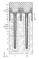
図1は、本実施形態に係る半導体装置を示す斜視図である。
図2は、本実施形態に係る半導体装置を示す断面図である。
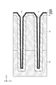
図3(a)及び図3(b)は、図2の領域A及び領域Bの拡大図である。
図1及び図2は、半導体装置100の斜視図及び断面図をそれぞれ示している。図2は、図1の半導体装置100の一部を拡大して示している。なお、図1において、ソース電極11及び柱状部60の図示が省略されている。
半導体装置100は、例えば、MOSFETである。
(First Embodiment)
FIG. 1 is a perspective view showing a semiconductor device according to the present embodiment.
FIG. 2 is a cross-sectional view showing a semiconductor device according to the present embodiment.
3A and 3B are enlarged views of the area A and the area B of FIG.
1 and 2 show a perspective view and a cross-sectional view of the
The
図1に示すように、半導体装置100には、ドレイン領域1と、第1導電形の半導体領域2と、第1導電形の半導体領域3と、第2導電形の半導体領域4と、第2導電形の半導体領域5と、第1導電形の半導体領域6と、コンタクト領域7と、ゲート電極8と、ゲートコンタクト9と、ドレイン電極10と、が設けられている。
ドレイン領域1の導電形は、例えばn+形である。
As shown in FIG. 1, the
The conductive type of the
n+、n、n−及びp+、p、p−の表記は、各導電形における実効的な不純物濃度の相対的な高低を表す。すなわち、「+」が付されている表記は、「+」及び「−」のいずれも付されていない表記よりも不純物濃度が相対的に高く、「−」が付されている表記は、いずれも付されていない表記よりも不純物濃度が相対的に低いことを示す。 The notations n + , n, n − and p + , p, p − represent the relative levels of effective impurity concentrations in each conductive form. That is, the notation with "+" has a relatively higher impurity concentration than the notation without either "+" or "-", and the notation with "-" is any of them. Indicates that the impurity concentration is relatively lower than the notation not marked with.
また、「実効的な不純物濃度」とは、半導体材料の導電性に寄与する不純物の濃度をいい、ドナーとなる不純物とアクセプタとなる不純物の双方が含まれている場合は、その相殺分を除いた濃度をいう。なお、n形不純物は、例えば、リン(P)であり、p形不純物は、例えば、ホウ素(B)である。 The "effective impurity concentration" means the concentration of impurities that contribute to the conductivity of the semiconductor material, and if both the donor impurity and the acceptor impurity are included, the offset is excluded. Impurity. The n-type impurity is, for example, phosphorus (P), and the p-type impurity is, for example, boron (B).
半導体領域2は、ドレイン領域1の上面1a上に設けられ、その導電形は、例えばn−形である。
半導体領域3は、半導体領域2上に複数設けられ、その導電形は、例えばn形である。半導体領域3は、例えば、nピラー領域である。複数の半導体領域3は、半導体領域2上に選択的に位置する。複数の半導体領域3は、X方向に延びており、Y方向に互いに離間して配置されている。
The
A plurality of
半導体領域4は、半導体領域2上に複数設けられ、その導電形は、例えばp形である。半導体領域4は、例えば、pピラー領域である。複数の半導体領域4は、半導体領域2上に選択的に位置する。複数の半導体領域4は、X方向に延びており、Y方向で隣り合う半導体領域3の間に位置するようにY方向に互いに離間して配置されている。
A plurality of
n形の半導体領域3と、p形の半導体領域4とは、Y方向において交互に設けられている。つまり、本実施形態の半導体装置100は、MOSFETであって、スーパージャンクション構造を有するものである。
The n-
半導体領域5は、半導体領域3上、及び、半導体領域4上に複数設けられ、その導電形は、例えばp形である。半導体領域5は、例えば、pベース領域である。複数の半導体領域5は、半導体領域3上に選択的に位置する。複数の半導体領域5は、X方向に延びており、Y方向に互いに離間して配置されている。
A plurality of
半導体領域6は、半導体領域5上に複数設けられ、その導電形は、例えばn+形である。半導体領域6は、例えば、ソース領域である。複数の半導体領域6は、半導体領域5上に選択的に位置する。複数の半導体領域6は、X方向に延びており、Y方向に互いに離間して配置されている。
A plurality of
コンタクト領域7は、半導体領域5上に複数設けられ、その導電形は、例えばp+形である。複数のコンタクト領域7は、半導体領域5上に選択的に位置する。複数のコンタクト領域7は、X方向に延びており、Y方向で隣り合う半導体領域6の間に位置するようにY方向に互いに離間して配置されている。コンタクト領域7は、後述するソース電極11に接続される。
A plurality of
ゲート電極8は、ゲート絶縁膜20(図2参照)を介して、半導体領域3上に複数設けられている。複数のゲート電極8は、半導体領域3上に選択的に位置する。
複数のゲート電極8は、X方向に延びており、Y方向で隣り合う半導体領域5の間に位置するようにY方向に互いに離間して配置されている。また、複数のゲート電極8は、Y方向で隣り合う半導体領域6の間に位置するようにY方向に互いに離間して配置されている。つまり、コンタクト領域7及びゲート電極8は、半導体領域6を介してY方向に交互に配置されている。
ゲート電極8は、例えば、n形不純物を含有した多結晶シリコンを含む。
A plurality of
The plurality of
The
ゲートコンタクト9は、ゲート電極8上に複数設けられている。複数のゲートコンタクト9は、Y方向に延びており、X方向に所定の間隔で配置されている。ゲートコンタクト9は、例えば、金属材料によって形成される。
A plurality of
ゲートコンタクト9を介して、ゲート電極8は、外部の周辺回路(図示せず)に電気的に接続される。ゲートコンタクト9を介して、ゲート電極8に閾値以上の電圧が印加されることで、MOSFETがオン状態となり、半導体領域5の表面にチャネル(反転層)が形成される。
ドレイン電極10は、ドレイン領域1の下面1b上に設けられている。ドレイン電極10は、ドレイン領域1に電気的に接続される。ドレイン電極10は、例えば、金属材料によって形成される。
The
The
図2に示すように、半導体領域6の一部上と、ゲート電極8の側面上及び底面上とには、ゲート絶縁膜20が設けられている。ゲート絶縁膜20は、例えば、シリコン酸化物(SiO)を含む。
ゲート電極8上、及び、ゲート絶縁膜20上には、層間絶縁膜21が設けられている。例えば、層間絶縁膜21は、膜21a及び膜21bの2層構造を有する。膜21aは、例えばシリコン酸化物を含む。膜21bは、膜21a上に設けられ、例えばBPSG(Boro-phospho silicate glass)を含む。
As shown in FIG. 2, a
An interlayer insulating
半導体領域4、5内には絶縁部30が設けられている。絶縁部30は、X方向に延びている。絶縁部30は、半導体領域2、3に形成されたトレンチT内に設けられている。トレンチTの内面上に、半導体領域4を介して絶縁部30が位置する。
An insulating
トレンチTは空隙部Vを含む。絶縁部30は、半導体領域4及び空隙部Vの間に位置する。
トレンチT内であって、空隙部V上にはカバー膜35が設けられている。カバー膜35は、例えばBPSGを含む。カバー膜35は、例えば、トレンチTにおけるキャップ膜として機能する。絶縁部30は、カバー膜35と、半導体領域4の一部及び半導体領域5との間に位置する。
絶縁部30及びカバー膜35は、内部に空隙部Vが形成された柱状部60を構成する。
The trench T includes a gap V. The insulating
A
The insulating
なお、図2に示す例では、カバー膜35は空隙部V上に設けられているが、空隙部Vの側面の少なくとも一部上に設けられても良い。つまり、カバー膜35は、Y方向において絶縁部30及び空隙部Vの間に位置しても良い。
In the example shown in FIG. 2, the
絶縁部30は、絶縁膜30aと、絶縁膜30bと、絶縁膜30cと、を有する。
絶縁膜30aは、例えば、シリコン酸化物(SiO)を含む。絶縁膜30bは、引張応力を有する材料、例えば、シリコン窒化物(SiN)を含む。絶縁膜30cは、例えば、シリコン酸化物(SiO)を含む。
絶縁膜30a、絶縁膜30b及び絶縁膜30cの形状は、例えば、底を有する筒状である。また、半導体領域4の形状は、例えば、底を有する筒状である。
The insulating
The insulating
The shapes of the insulating
図3(a)に示すように、絶縁膜30aは、半導体領域4の側面上に位置する。絶縁膜30bは、絶縁膜30aの側面上に位置する。絶縁膜30cは、絶縁膜30bの側面上に位置する。絶縁部30は、カバー膜35の側面、及び、空隙部Vの側面を覆っており、絶縁膜30c、30b、30aがこれらの側面から離れる方向にこの順で位置する。
As shown in FIG. 3A, the insulating
図3(b)に示すように、絶縁膜30aは、半導体領域4の底面上に位置する。絶縁膜30bは、絶縁膜30aの底面上に位置する。絶縁膜30cは、絶縁膜30bの底面上に位置する。絶縁部30は、空隙部Vの底面を覆っており、絶縁膜30c、30b、30aがこの底面から離れる方向にこの順で位置する。
As shown in FIG. 3B, the insulating
絶縁部30内の膜厚においては、絶縁膜30aを絶縁膜30b及び絶縁膜30cより大きくして、絶縁膜30bを絶縁膜30cより大きくすることが可能である。また、絶縁膜30aの膜厚を薄くして、絶縁膜30cをCVD(Chemical Vapor Deposition)膜により形成しても良い。この場合、絶縁膜30cを絶縁膜30a及び絶縁膜30bより大きくして、絶縁膜30bを絶縁膜30aより大きくすることが可能である。なお、絶縁膜30cをCVD膜によって形成する代わりに、他の被覆性の良い材料を用いて形成しても良い。
絶縁膜30aと絶縁膜30cの合計膜厚は、絶縁膜30bの膜厚の0.5倍以上であって4倍以下である。絶縁膜30aと絶縁膜30cの合計膜厚は、絶縁膜30bの膜厚の1倍以上(または同等以上)であって4倍以下であれば、さらに望ましい。絶縁膜30aと絶縁膜30cが、例えばシリコン酸化物(SiO)を含み、絶縁膜30bが、例えばシリコン窒化物(SiN)を含む場合、絶縁膜30aと絶縁膜30cの合計膜厚は、絶縁膜30bの膜厚の1.8倍程度であることが望ましい。
Regarding the film thickness in the insulating
The total film thickness of the insulating
絶縁膜30a、30b、30cの膜厚とは、半導体領域4の側面上に絶縁膜30a、30b、30cが順に位置する場合(図3(a)の場合)、絶縁膜30a、30b、30cのY方向の厚さに相当し、半導体領域4の底面上に絶縁膜30a、30b、30cが順に位置する場合(図3(b)の場合)、絶縁膜30a、30b、30cのZ方向の厚さに相当する。
The film thickness of the insulating
絶縁膜30aは、例えば、半導体領域3及び半導体領域4を保護する。絶縁膜30bは、例えば、絶縁膜30aの応力(例えば、圧縮応力)を緩和させる。絶縁膜30cは、例えば、トレンチT内にカバー膜35を埋め込み易くする。
The insulating
図2に示すように、半導体領域6の一部上と、コンタクト領域7上と、層間絶縁膜21の側面上及び上面上とには、ソース電極11が設けられている。また、ソース電極11は、絶縁部30上及びカバー膜35上に設けられている。ソース電極11は、例えば、金属材料によって形成される。
ソース電極11上には、層間絶縁膜22が設けられている。層間絶縁膜22は、例えば、シリコン酸化物を含む。
As shown in FIG. 2,
An interlayer insulating
次に、本実施形態に係る半導体装置の製造方法について説明する。
図4〜図9は、半導体装置100の製造方法を示す断面図である。
なお、図4〜図9に示された領域は、図2に示された領域の一部に相当する。なお、図4〜図9においては、柱状部60より上の部分、及び、半導体領域2より下の部分は示されていない。
まず、図4に示すように、第1導電形の半導体基板40上に、第1導電形の半導体層41をエピタキシャル成長させる。
Next, a method of manufacturing the semiconductor device according to the present embodiment will be described.
4 to 9 are cross-sectional views showing a method of manufacturing the
The region shown in FIGS. 4 to 9 corresponds to a part of the region shown in FIG. In addition, in FIGS. 4 to 9, the portion above the
First, as shown in FIG. 4, the first conductive type semiconductor layer 41 is epitaxially grown on the first conductive type semiconductor substrate 40.
続いて、半導体層41上に、シリコン酸化膜等を含むマスク材を形成する。例えば、マスク材は、CVD法により半導体層41上に膜を堆積した後、リソグラフィ法及びRIE(Reactive Ion Etching)法により形成される。 Subsequently, a mask material containing a silicon oxide film or the like is formed on the semiconductor layer 41. For example, the mask material is formed by a lithography method and a RIE (Reactive Ion Etching) method after depositing a film on the semiconductor layer 41 by a CVD method.
続いて、パターニングされたマスク材をマスクに、半導体基板40及び半導体層41にトレンチTを形成する。トレンチTは、例えば、RIE法により形成される。その後、マスク材を剥離する。なお、トレンチTを形成した後の半導体基板40は、半導体領域2に相当する。また、トレンチTを形成した後の半導体層41は、半導体領域3に相当する。
Subsequently, a trench T is formed in the semiconductor substrate 40 and the semiconductor layer 41 using the patterned mask material as a mask. The trench T is formed by, for example, the RIE method. After that, the mask material is peeled off. The semiconductor substrate 40 after forming the trench T corresponds to the
次に、図5に示すように、トレンチTの内壁面上及び底面上に、エピタキシャル成長法により、p形不純物を含む半導体膜42を形成する。半導体膜42は、トレンチT間の半導体領域3上にも形成される。半導体膜42は、例えば、ノンドープの単結晶シリコンを含む。半導体膜42は、半導体領域4に相当する。
Next, as shown in FIG. 5, a
続いて、トレンチT内であって半導体領域4の側面及び底面に、例えば熱酸化により、絶縁膜30aを形成する。絶縁膜30aは、トレンチT間の半導体領域4にも形成される。例えば、絶縁膜30aは、シリコン酸化物によって形成される。
Subsequently, an insulating
次に、図6に示すように、トレンチT内であって絶縁膜30aの側面上及び底面上に、例えばLPCVD(Low Pressure Chemical Vapor Deposition)法により、絶縁膜30bを形成する。絶縁膜30bは、トレンチT間の絶縁膜30a上にも形成される。例えば、絶縁膜30bは、シリコン窒化物によって形成される。
Next, as shown in FIG. 6, the insulating
続いて、トレンチT内であって絶縁膜30bの側面及び底面に、例えば熱酸化により、絶縁膜30cを形成する。絶縁膜30cは、トレンチT間の絶縁膜30bにも形成される。例えば、絶縁膜30cは、シリコン酸化物によって形成される。
Subsequently, the insulating
次に、図7に示すように、トレンチTを埋め込むように、絶縁膜30c上に、例えばCVD法により、カバー膜35を形成する。例えば、カバー膜35は、BPSGによって形成される。これにより、トレンチT内に、カバー膜35が上に位置する空隙部Vが形成される。続いて、カバー膜35にリフロー及びアニール処理を施す。
Next, as shown in FIG. 7, a
絶縁膜30bの側面上及び底面上に絶縁膜30c(シリコン酸化膜)が形成されているので、トレンチTの上部にカバー膜35が形成され易い。つまり、絶縁膜30cによって、トレンチTの深さ方向(−Z方向)におけるカバー膜35の埋め込み性が向上する。
Since the insulating
次に、図8に示すように、エッチング処理を施してカバー膜35の一部を除去する。トレンチT上、及び、トレンチT間に位置するカバー膜35を除去するようにエッチバックする。続いて、例えばCDE(Chemical Dry Etching)法により、トレンチT間の絶縁膜30a上に位置する絶縁膜30b、30cを除去する。
Next, as shown in FIG. 8, a part of the
次に、図9に示すように、エッチング処理を施して、トレンチT間の半導体領域4上に位置する絶縁膜30aを除去する。続いて、例えばCMP(Chemical Mechanical Polishing)法により、半導体領域3の一部、及び、半導体領域4の一部を除去する。これにより、絶縁膜30a、30b、30cの上面、及び、カバー膜35の上面が平坦化され、絶縁膜30a、絶縁膜30b及び絶縁膜30cを有する絶縁部30が形成される。
Next, as shown in FIG. 9, an etching process is performed to remove the insulating
その後、公知の製造方法により、半導体領域5、6と、コンタクト領域7と、ゲート絶縁膜20と、ゲート電極8と、を形成する。続いて、層間絶縁膜21と、ソース電極11と、層間絶縁膜22と、ゲートコンタクト9と、ドレイン電極10と、を形成することで、半導体装置100が形成される。
After that, the
次に、本実施形態の効果について説明する。
n形半導体領域とp形半導体領域とがトレンチを介して交互に設けられたスーパージャンクション構造を有するMOSFETでは、セルのピッチの微細化に伴って高アスペクト比のトレンチが形成され易い。トレンチの内面上及び上部上には、p形半導体領域及びカバー膜がそれぞれ形成され、トレンチの一部(p形半導体領域及びカバー膜で囲まれた部分)には空隙部が形成される場合がある。
Next, the effect of this embodiment will be described.
In a MOSFET having a super junction structure in which n-type semiconductor regions and p-type semiconductor regions are alternately provided via trenches, trenches having a high aspect ratio are likely to be formed as the cell pitch becomes finer. A p-type semiconductor region and a cover film may be formed on the inner surface and the upper portion of the trench, respectively, and a gap may be formed in a part of the trench (the portion surrounded by the p-type semiconductor region and the cover film). is there.
このようなMOSFETでは、p形半導体領域から空隙部に電流が漏れ易くなる。空隙部へのリーク電流によってMOSFETの動作に不具合が生じる虞がある。また、トレンチの上部上にカバー膜を形成する場合、カバー膜が側面に位置する膜の材料によってはトレンチに対するカバー膜の埋め込み性が低下し易くなる。 In such a MOSFET, a current easily leaks from the p-type semiconductor region to the gap portion. Leakage current to the gap may cause a malfunction in the operation of the MOSFET. Further, when the cover film is formed on the upper part of the trench, the embedding property of the cover film in the trench tends to decrease depending on the material of the film in which the cover film is located on the side surface.
また、カバー膜に含まれるホウ素やリン等の不純物がn形半導体領域及びp形半導体領域に染み出す場合があり、これらの半導体領域を保護するためにp形半導体領域の側壁に厚い膜を形成することが考えられる。しかし、p形半導体領域の側壁に圧縮応力を有する膜(例えば、シリコン酸化膜)を形成すると、圧縮応力を有する膜が厚く形成されることでウェーハの反りが大きくなってしまう。ウェーハの大きな反りは、製造工程中における加工精度を低下させ、製造装置の安定した稼働を妨げる原因となる。 In addition, impurities such as boron and phosphorus contained in the cover film may seep into the n-type semiconductor region and the p-type semiconductor region, and a thick film is formed on the side wall of the p-type semiconductor region to protect these semiconductor regions. It is conceivable to do. However, when a film having compressive stress (for example, a silicon oxide film) is formed on the side wall of the p-type semiconductor region, the film having compressive stress is formed thickly, so that the warp of the wafer becomes large. The large warp of the wafer lowers the processing accuracy during the manufacturing process and causes the stable operation of the manufacturing equipment to be hindered.
本実施形態の半導体装置100において、トレンチT内の半導体領域4上に絶縁膜30a、30b、30cが順に設けられている。このような絶縁膜30a、30b、30c(例えば、ONO膜)を設けると、半導体領域4から空隙部Vに電流が漏れることを抑制する。
In the
また、本実施形態では、絶縁膜30aによってカバー膜35の不純物等から半導体領域3及び半導体領域4を保護する。そして、絶縁膜30bは引張応力を有する材料(例えば、シリコン窒化物)を含むので、絶縁膜30bによって絶縁膜30aの応力を相殺してウェーハの反りを抑制する。例えば、絶縁膜30aの膜厚と、絶縁膜30bの膜厚とを所定の比率になるように設定すると(例えば、絶縁膜30aと絶縁膜30cの合計膜厚を絶縁膜30bの膜厚の1.8倍程度にすると)、カバー膜35の不純物の染み出しと、ウェーハの反りとがより抑制される。
Further, in the present embodiment, the
また、本実施形態では、絶縁膜30cは、例えばシリコン酸化物を含むので、絶縁膜30cの側面上にカバー膜35が形成され易くなる。つまり、トレンチTに対するカバー膜35の埋め込み性が向上する。
本実施形態によれば、信頼性が向上した半導体装置及びその製造方法を提供することができる。
Further, in the present embodiment, since the insulating
According to this embodiment, it is possible to provide a semiconductor device having improved reliability and a method for manufacturing the same.
(第2実施形態)
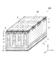
図10は、本実施形態に係る半導体装置を示す斜視図である。
図10は、半導体装置200を示す斜視図である。図10に示された領域は、図1に示された領域に相当する。なお、図10において、ソース電極11及び柱状部60の図示が省略されている。
本実施形態において、半導体領域3及び半導体領域4より上の構成が第1実施形態と異なる。よって、これ以外の構成の詳細な説明は省略する。
(Second Embodiment)
FIG. 10 is a perspective view showing a semiconductor device according to the present embodiment.
FIG. 10 is a perspective view showing the
In the present embodiment, the configurations above the
図10に示すように、半導体装置200には、ドレイン領域1と、半導体領域2と、半導体領域3と、半導体領域4と、半導体領域5と、半導体領域6と、コンタクト領域7と、ゲート電極8と、ゲートコンタクト9と、ドレイン電極10と、が設けられている。
As shown in FIG. 10, the
半導体領域5は、半導体領域3上、及び、半導体領域4上に複数設けられている。複数の半導体領域5は、X−Y平面を島状に配置されている。
半導体領域6は、半導体領域5上に複数設けられている。複数の半導体領域6は、X−Y平面を島状に配置されている。
A plurality of
A plurality of
コンタクト領域7は、半導体領域5上に複数設けられている。複数のコンタクト領域7は、X−Y平面を島状に配置されている。また、複数のコンタクト領域7は、Y方向で隣り合う半導体領域6の間に位置するようにY方向に互いに離間して配置されている。
半導体領域5、半導体領域6及びコンタクト領域7をそれぞれ有する複数の領域50は、X−Y平面を島状に配置されている。
A plurality of
The plurality of
ゲート電極8は、半導体領域3上に格子状に設けられている。ゲート電極8は、X方向及びY方向で隣り合う半導体領域5の間に位置する。
ゲートコンタクト9は、ゲート電極8上に設けられている。
The
The
本実施形態において、絶縁部30の構成及び配置は第1実施形態と同じである。つまり、図2、図3(a)及び図3(b)に示すように、絶縁部30は、絶縁膜30a、30b、30cを有し、半導体領域4、5内に設けられている。
本実施形態の効果は、前述の第1実施形態と同じである。
In the present embodiment, the configuration and arrangement of the insulating
The effect of this embodiment is the same as that of the first embodiment described above.
(第3実施形態)
図11は、本実施形態に係る半導体装置を示す断面図である。
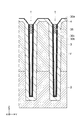
図12は、図11の領域Cの拡大図である。
図11に示すように、半導体装置300には、ドレイン領域1と、半導体領域2と、半導体領域3と、半導体領域4と、半導体領域5と、半導体領域6と、ゲート電極8と、ドレイン電極10と、ソース電極11と、ゲート絶縁膜20と、層間絶縁膜21と、絶縁部30と、カバー膜35と、が設けられている。層間絶縁膜21は、膜21a及び膜21bを有する。
(Third Embodiment)
FIG. 11 is a cross-sectional view showing a semiconductor device according to the present embodiment.
FIG. 12 is an enlarged view of the region C of FIG.
As shown in FIG. 11, the
半導体領域2は、ドレイン領域1の上面1a上に設けられている。
半導体領域3は、半導体領域2上に複数設けられている。複数の半導体領域3は、X方向に延びており、Y方向に互いに離間して配置されている。
半導体領域4は、半導体領域2上に複数設けられている。複数の半導体領域4は、X方向に延びており、Y方向で隣り合う半導体領域3の間に位置するようにY方向に互いに離間して配置されている。
The
A plurality of
A plurality of
複数の半導体領域3及び複数の半導体領域4は、多段エピタキシャル法を用いて形成される。例えば、リソグラフィ法を用いたイオン注入と、エピタキシャル成長法とをZ方向に交互に繰り返す。これにより、n形の半導体領域3と、p形の半導体領域4とがY方向において交互に位置するように半導体領域2上に設けられる。つまり、本実施形態の半導体装置300は、MOSFETであって、スーパージャンクション構造を有するものである。
The plurality of
半導体領域5は、半導体領域3上、及び、半導体領域4上に複数設けられている。複数の半導体領域5は、Y方向に互いに離間して配置されている。
半導体領域6は、半導体領域5上に複数設けられている。複数の半導体領域6は、Y方向に互いに離間して配置されている。
A plurality of
A plurality of
ゲート電極8は、半導体領域3上にゲート絶縁膜20を介して複数設けられている。複数のゲート電極8は、Y方向に互いに離間して配置されている。
ドレイン電極10は、ドレイン領域1の下面1b上に設けられている。
ソース電極11は、半導体領域5の一部上と、半導体領域6の一部上と、層間絶縁膜21上と、絶縁部30上と、カバー膜35上とに設けられている。
A plurality of
The
The
絶縁部30は、トレンチT1内に設けられている。トレンチT1は、破線で示すように、半導体領域2、半導体領域3、半導体領域5及び半導体領域6からなる半導体領域51と、半導体領域2、半導体領域4及び半導体領域5からなる半導体領域52との間に形成される。トレンチT1の内面上に絶縁部30が位置する。
The insulating
カバー膜35は、トレンチT1の空隙部V上に設けられている。絶縁部30は、半導体領域51と、空隙部V及びカバー膜35との間に位置する。また、絶縁部30は、半導体領域52と、空隙部V及びカバー膜35との間に位置する。
The
図12に示すように、絶縁部30は、絶縁膜30a、絶縁膜30b及び絶縁膜30cを有する。
絶縁膜30aは、半導体領域51の側面上、及び、半導体領域52の側面上に位置する。また、絶縁膜30aは、トレンチT1の底面上であって半導体領域2上に位置する。
絶縁膜30bは、絶縁膜30aの側面上及び底面上に位置する。
絶縁膜30cは、絶縁膜30bの側面上及び底面上に位置する。
つまり、絶縁部30は、カバー膜35の側面と、空隙部Vの側面及び底面とを覆っており、絶縁膜30c、30b、30aがこれらの側面及び底面から離れる方向にこの順で位置する。絶縁膜30a、絶縁膜30b及び絶縁膜30cの形状は、例えば、底を有する筒状である。
本実施形態の効果は、前述の第1実施形態と同じである。
As shown in FIG. 12, the insulating
The insulating
The insulating
The insulating
That is, the insulating
The effect of this embodiment is the same as that of the first embodiment described above.
前述したように、一例として、スーパージャンクション構造を有するMOSFETを例に説明したが、各実施形態に係る半導体装置は、スーパージャンクション構造を有するIGBT(Insulated Gate Bipolar Transistor)等、その他の半導体装置に適用しても良い。 As described above, a MOSFET having a super junction structure has been described as an example, but the semiconductor device according to each embodiment is applied to other semiconductor devices such as an IGBT (Insulated Gate Bipolar Transistor) having a super junction structure. You may.
以上、本発明のいくつかの実施形態を説明したが、これらの実施形態は、例として提示したものであり、発明の範囲を限定することは意図していない。これらの新規な実施形態は、その他の様々な形態で実施されることが可能であり、発明の要旨を逸脱しない範囲で、種々の省略、置き換え、変更を行うことができる。これら実施形態やその変形は、発明の範囲や要旨に含まれるとともに、特許請求の範囲に記載された発明及びその等価物の範囲に含まれる。 Although some embodiments of the present invention have been described above, these embodiments are presented as examples and are not intended to limit the scope of the invention. These novel embodiments can be implemented in various other embodiments, and various omissions, replacements, and changes can be made without departing from the gist of the invention. These embodiments and modifications thereof are included in the scope and gist of the invention, and are also included in the scope of the invention and its equivalents described in the claims.
1:ドレイン領域、1a:上面、1b:下面、2〜6、51、52:半導体領域、7:コンタクト領域、8:ゲート電極、9:ゲートコンタクト、10:ドレイン電極、11:ソース電極、20:ゲート絶縁膜、21、22:層間絶縁膜、21a、21b:膜、30:絶縁部、30a、30b、30c:絶縁膜、35:カバー膜、40:半導体基板、41:半導体層、42:半導体膜、50:領域、60:柱状部、100、200、300:半導体装置、T、T1:トレンチ、V:空隙部 1: Drain region, 1a: Top surface, 1b: Bottom surface, 2-6, 51, 52: Semiconductor region, 7: Contact region, 8: Gate electrode, 9: Gate contact, 10: Drain electrode, 11: Source electrode, 20 : Gate insulating film, 21, 22: interlayer insulating film, 21a, 21b: film, 30: insulating part, 30a, 30b, 30c: insulating film, 35: cover film, 40: semiconductor substrate, 41: semiconductor layer, 42: Semiconductor film, 50: region, 60: columnar portion, 100, 200, 300: semiconductor device, T, T1: trench, V: void portion
Claims (4)
前記第1方向に延び、前記第1方向に交差する第2方向に前記第1半導体領域と配置され、空隙を囲む第2導電形の第2半導体領域と、
前記空隙と、前記第2半導体領域との間に設けられ、シリコン酸化物を含む第1絶縁膜と、シリコン窒化物を含む第2絶縁膜と、シリコン酸化物を含む第3絶縁膜とを有する絶縁部と、
を備え、
前記第1絶縁膜、前記第2絶縁膜及び前記第3絶縁膜は、前記第2半導体領域から前記空隙に向かって順に位置し、
前記第1絶縁膜と前記第3絶縁膜の厚さの合計は、前記第2絶縁膜の厚さの0.5倍以上であって4倍以下である半導体装置。 The first conductive type first semiconductor region extending in the first direction,
A second conductive type second semiconductor region extending in the first direction, arranged with the first semiconductor region in the second direction intersecting the first direction, and surrounding the gap,
It has a first insulating film containing a silicon oxide, a second insulating film containing a silicon nitride, and a third insulating film containing a silicon oxide, which are provided between the gap and the second semiconductor region. Insulation part and
With
The first insulating film, the second insulating film, and the third insulating film are located in order from the second semiconductor region toward the void .
A semiconductor device in which the total thickness of the first insulating film and the third insulating film is 0.5 times or more and 4 times or less the thickness of the second insulating film .
前記第2絶縁膜は、前記第1絶縁膜の側面上及び底面上に位置し、
前記第3絶縁膜は、前記第2絶縁膜の側面上及び底面上に位置する請求項1記載の半導体装置。 The first insulating film is located on the side surface and the bottom surface of the second semiconductor region.
The second insulating film is located on the side surface and the bottom surface of the first insulating film.
The third insulating film, a semiconductor device according to claim 1, wherein located on the side and on the bottom surface of the second insulating film.
前記空隙上に設けられ、前記第3半導体領域との間で前記絶縁部が位置するカバー膜と、
をさらに備えた請求項1または2に記載の半導体装置。 The first semiconductor region, the second conductive type third semiconductor region provided on the second semiconductor region, and the third semiconductor region.
A cover film provided on the gap and having the insulating portion located between the third semiconductor region and the third semiconductor region.
The semiconductor device according to claim 1 or 2 , further comprising.
前記第1方向に延び、前記第1方向に交差する第2方向に空隙を介して前記第1半導体領域と配置される第2導電形の第2半導体領域と、
前記空隙と、前記第1半導体領域及び前記第2半導体領域との間に設けられ、シリコン酸化物を含む第1絶縁膜と、シリコン窒化物を含む第2絶縁膜と、シリコン酸化物を含む第3絶縁膜とを有する絶縁部と、
を備えた半導体装置。 The first conductive type first semiconductor region extending in the first direction,
A second conductive type second semiconductor region extending in the first direction and arranged with the first semiconductor region through a gap in the second direction intersecting the first direction.
A first insulating film provided between the void and the first semiconductor region and the second semiconductor region and containing a silicon oxide, a second insulating film containing a silicon nitride, and a second insulating film containing a silicon oxide. Insulation part having 3 insulating films and
Semiconductor device equipped with.
Priority Applications (3)
| Application Number | Priority Date | Filing Date | Title |
|---|---|---|---|
| JP2017102560A JP6817895B2 (en) | 2017-05-24 | 2017-05-24 | Semiconductor device |
| CN201710790536.1A CN108962993B (en) | 2017-05-24 | 2017-09-05 | Semiconductor device and method for manufacturing the same |
| US15/876,412 US10431491B2 (en) | 2017-05-24 | 2018-01-22 | Semiconductor device having a triple insulating film surrounded void |
Applications Claiming Priority (1)
| Application Number | Priority Date | Filing Date | Title |
|---|---|---|---|
| JP2017102560A JP6817895B2 (en) | 2017-05-24 | 2017-05-24 | Semiconductor device |
Publications (3)
| Publication Number | Publication Date |
|---|---|
| JP2018198267A JP2018198267A (en) | 2018-12-13 |
| JP2018198267A5 JP2018198267A5 (en) | 2019-10-03 |
| JP6817895B2 true JP6817895B2 (en) | 2021-01-20 |
Family
ID=64401126
Family Applications (1)
| Application Number | Title | Priority Date | Filing Date |
|---|---|---|---|
| JP2017102560A Active JP6817895B2 (en) | 2017-05-24 | 2017-05-24 | Semiconductor device |
Country Status (3)
| Country | Link |
|---|---|
| US (1) | US10431491B2 (en) |
| JP (1) | JP6817895B2 (en) |
| CN (1) | CN108962993B (en) |
Families Citing this family (6)
| Publication number | Priority date | Publication date | Assignee | Title |
|---|---|---|---|---|
| US10903331B2 (en) * | 2019-03-25 | 2021-01-26 | International Business Machines Corporation | Positioning air-gap spacers in a transistor for improved control of parasitic capacitance |
| JP7317752B2 (en) | 2020-03-17 | 2023-07-31 | 株式会社東芝 | semiconductor equipment |
| JP2022135310A (en) * | 2021-03-05 | 2022-09-15 | 株式会社東芝 | Semiconductor device and manufacturing method for the same |
| US20230051830A1 (en) * | 2021-08-13 | 2023-02-16 | Infineon Technologies Ag | Semiconductor device and method of producing thereof |
| DE102021121138B3 (en) * | 2021-08-13 | 2023-02-02 | Infineon Technologies Ag | SEMICONDUCTOR DEVICES AND METHOD OF MANUFACTURING A SEMICONDUCTOR DEVICE |
| CN115775823B (en) * | 2022-11-29 | 2023-07-21 | 上海功成半导体科技有限公司 | Shielding grid power device and preparation method thereof |
Family Cites Families (34)
| Publication number | Priority date | Publication date | Assignee | Title |
|---|---|---|---|---|
| US5937296A (en) * | 1996-12-20 | 1999-08-10 | Siemens Aktiengesellschaft | Memory cell that includes a vertical transistor and a trench capacitor |
| DE19748523C2 (en) | 1997-11-03 | 1999-10-07 | Siemens Ag | Semiconductor component, method for producing such a semiconductor component and use of the method |
| US6337499B1 (en) * | 1997-11-03 | 2002-01-08 | Infineon Technologies Ag | Semiconductor component |
| JP2000196074A (en) * | 1998-12-25 | 2000-07-14 | Toshiba Corp | Semiconductor device and its manufacture |
| FR2795554B1 (en) * | 1999-06-28 | 2003-08-22 | France Telecom | HOLES LATERAL ENGRAVING METHOD FOR MANUFACTURING SEMICONDUCTOR DEVICES |
| JP4285899B2 (en) | 2000-10-10 | 2009-06-24 | 三菱電機株式会社 | Semiconductor device having groove |
| US6521954B1 (en) * | 2001-12-21 | 2003-02-18 | Kabushiki Kaisha Toshiba | Semiconductor device and manufacturing method thereof |
| JP3993458B2 (en) * | 2002-04-17 | 2007-10-17 | 株式会社東芝 | Semiconductor device |
| JP3634848B2 (en) * | 2003-01-07 | 2005-03-30 | 株式会社東芝 | Power semiconductor device |
| JP2006066611A (en) * | 2004-08-26 | 2006-03-09 | Toshiba Corp | Semiconductor device |
| JP4830285B2 (en) * | 2004-11-08 | 2011-12-07 | 株式会社デンソー | Method for manufacturing silicon carbide semiconductor device |
| JP5011881B2 (en) * | 2006-08-11 | 2012-08-29 | 株式会社デンソー | Manufacturing method of semiconductor device |
| JP2008210940A (en) * | 2007-02-26 | 2008-09-11 | Elpida Memory Inc | Semiconductor device and manufacturing method thereof |
| JP5583315B2 (en) * | 2007-07-19 | 2014-09-03 | ピーエスフォー ルクスコ エスエイアールエル | Semiconductor device and manufacturing method thereof |
| JP4973418B2 (en) * | 2007-09-26 | 2012-07-11 | サンケン電気株式会社 | Semiconductor device |
| US7956411B2 (en) * | 2008-01-15 | 2011-06-07 | Fairchild Semiconductor Corporation | High aspect ratio trench structures with void-free fill material |
| US7960781B2 (en) * | 2008-09-08 | 2011-06-14 | Semiconductor Components Industries, Llc | Semiconductor device having vertical charge-compensated structure and sub-surface connecting layer and method |
| JP5400405B2 (en) * | 2009-02-05 | 2014-01-29 | 株式会社東芝 | Manufacturing method of semiconductor device |
| US8319278B1 (en) * | 2009-03-31 | 2012-11-27 | Maxpower Semiconductor, Inc. | Power device structures and methods using empty space zones |
| KR101802220B1 (en) * | 2010-12-20 | 2017-11-29 | 삼성전자주식회사 | Semiconductor devices including a vertical channel transistor and methods of fabricating the same |
| WO2013001677A1 (en) * | 2011-06-28 | 2013-01-03 | パナソニック株式会社 | Semiconductor device and method for manufacturing same |
| US8907408B2 (en) * | 2012-03-26 | 2014-12-09 | Infineon Technologies Austria Ag | Stress-reduced field-effect semiconductor device and method for forming therefor |
| US9070580B2 (en) * | 2013-05-01 | 2015-06-30 | Infineon Technologies Austria Ag | Semiconductor device with a super junction structure based on a compensation structure with compensation layers and having a compensation rate gradient |
| US9024383B2 (en) * | 2013-05-01 | 2015-05-05 | Infineon Technologies Austria Ag | Semiconductor device with a super junction structure with one, two or more pairs of compensation layers |
| KR102078852B1 (en) * | 2013-08-29 | 2020-02-18 | 삼성전자 주식회사 | Semiconductor devices and method of manufacturing the same |
| US9560765B2 (en) * | 2013-12-06 | 2017-01-31 | Infineon Technologies Dresden Gmbh | Electronic device, a method for manufacturing an electronic device, and a method for operating an electronic device |
| US9953861B2 (en) * | 2014-11-26 | 2018-04-24 | Taiwan Semiconductor Manufacturing Company, Ltd. | Semiconductor device having a shallow trench isolation structure and methods of forming the same |
| US9666507B2 (en) * | 2014-11-30 | 2017-05-30 | United Microelectronics Corp. | Through-substrate structure and method for fabricating the same |
| JP2016139676A (en) * | 2015-01-27 | 2016-08-04 | トヨタ自動車株式会社 | Semiconductor device and manufacturing method of the same |
| US9379043B1 (en) * | 2015-02-10 | 2016-06-28 | Powertech Technology Inc. | TSV structure having insulating layers with embedded voids |
| JP6509635B2 (en) * | 2015-05-29 | 2019-05-08 | 東芝メモリ株式会社 | Semiconductor device and method of manufacturing semiconductor device |
| JP6301882B2 (en) * | 2015-08-21 | 2018-03-28 | トヨタ自動車株式会社 | Semiconductor device manufacturing method and semiconductor device |
| US9929271B2 (en) * | 2016-08-03 | 2018-03-27 | Taiwan Semiconductor Manufacturing Company, Ltd. | Semiconductor device and method |
| JP2018046251A (en) * | 2016-09-16 | 2018-03-22 | 株式会社東芝 | Semiconductor device and method of manufacturing the same |
-
2017
- 2017-05-24 JP JP2017102560A patent/JP6817895B2/en active Active
- 2017-09-05 CN CN201710790536.1A patent/CN108962993B/en active Active
-
2018
- 2018-01-22 US US15/876,412 patent/US10431491B2/en active Active
Also Published As
| Publication number | Publication date |
|---|---|
| JP2018198267A (en) | 2018-12-13 |
| CN108962993A (en) | 2018-12-07 |
| US10431491B2 (en) | 2019-10-01 |
| CN108962993B (en) | 2021-09-24 |
| US20180342415A1 (en) | 2018-11-29 |
Similar Documents
| Publication | Publication Date | Title |
|---|---|---|
| JP6817895B2 (en) | Semiconductor device | |
| US8269272B2 (en) | Semiconductor device and method for manufacturing the same | |
| US10319850B2 (en) | Semiconductor device and manufacturing method of semiconductor device | |
| JP2017162909A (en) | Semiconductor device | |
| JP5298565B2 (en) | Semiconductor device and manufacturing method thereof | |
| JP6378220B2 (en) | Semiconductor device | |
| JP2018129378A (en) | Semiconductor device and method of manufacturing the same, and semiconductor wafer structure | |
| JP2013258327A (en) | Semiconductor device and method of manufacturing the same | |
| JP2007242852A (en) | Insulated gate semiconductor device and method of manufacturing same | |
| JP6193163B2 (en) | Insulated gate semiconductor device | |
| JP4735235B2 (en) | Insulated gate semiconductor device and manufacturing method thereof | |
| JP2017045776A (en) | Semiconductor device and manufacturing method of the same | |
| JP6312933B2 (en) | Power semiconductor device | |
| JP2015050390A (en) | Semiconductor device | |
| TWI590449B (en) | Silicon carbide semiconductor device, method of manufacturing the silicon carbide semiconductor device, and method of designing the silicon carbide semiconductor device | |
| JP2019003967A (en) | Semiconductor device and method of manufacturing the same | |
| JP2005322700A (en) | Manufacturing method of semiconductor device | |
| JP2017188590A (en) | Semiconductor device and manufacturing method of the same | |
| JP2015146399A (en) | Semiconductor device and semiconductor device manufacturing method | |
| JP6958575B2 (en) | Semiconductor devices and their manufacturing methods | |
| JP2006202940A (en) | Semiconductor device and its manufacturing method | |
| JP2008306022A (en) | Semiconductor device | |
| JP2016219495A (en) | Semiconductor device and manufacturing method thereof | |
| TWI574405B (en) | Silicon carbide semiconductor device, method for manufacturing silicon carbide semiconductor device, and design method of silicon carbide semiconductor device | |
| JP2018152522A (en) | Semiconductor device and method of manufacturing the same |
Legal Events
| Date | Code | Title | Description |
|---|---|---|---|
| A711 | Notification of change in applicant |
Free format text: JAPANESE INTERMEDIATE CODE: A712 Effective date: 20171116 |
|
| A711 | Notification of change in applicant |
Free format text: JAPANESE INTERMEDIATE CODE: A711 Effective date: 20171117 |
|
| A521 | Request for written amendment filed |
Free format text: JAPANESE INTERMEDIATE CODE: A523 Effective date: 20190809 |
|
| A621 | Written request for application examination |
Free format text: JAPANESE INTERMEDIATE CODE: A621 Effective date: 20190809 |
|
| A977 | Report on retrieval |
Free format text: JAPANESE INTERMEDIATE CODE: A971007 Effective date: 20200630 |
|
| A131 | Notification of reasons for refusal |
Free format text: JAPANESE INTERMEDIATE CODE: A131 Effective date: 20200730 |
|
| A521 | Request for written amendment filed |
Free format text: JAPANESE INTERMEDIATE CODE: A523 Effective date: 20200916 |
|
| TRDD | Decision of grant or rejection written | ||
| A01 | Written decision to grant a patent or to grant a registration (utility model) |
Free format text: JAPANESE INTERMEDIATE CODE: A01 Effective date: 20201127 |
|
| A61 | First payment of annual fees (during grant procedure) |
Free format text: JAPANESE INTERMEDIATE CODE: A61 Effective date: 20201225 |
|
| R150 | Certificate of patent or registration of utility model |
Ref document number: 6817895 Country of ref document: JP Free format text: JAPANESE INTERMEDIATE CODE: R150 |