JP6657537B2 - 半導体レーザ素子及び半導体レーザ素子の製造方法 - Google Patents
半導体レーザ素子及び半導体レーザ素子の製造方法 Download PDFInfo
- Publication number
- JP6657537B2 JP6657537B2 JP2015088507A JP2015088507A JP6657537B2 JP 6657537 B2 JP6657537 B2 JP 6657537B2 JP 2015088507 A JP2015088507 A JP 2015088507A JP 2015088507 A JP2015088507 A JP 2015088507A JP 6657537 B2 JP6657537 B2 JP 6657537B2
- Authority
- JP
- Japan
- Prior art keywords
- diffraction grating
- layer
- semiconductor laser
- laser device
- width
- Prior art date
- Legal status (The legal status is an assumption and is not a legal conclusion. Google has not performed a legal analysis and makes no representation as to the accuracy of the status listed.)
- Active
Links
- 239000004065 semiconductor Substances 0.000 title claims description 94
- 238000004519 manufacturing process Methods 0.000 title claims description 34
- 230000003287 optical effect Effects 0.000 claims description 44
- 238000000034 method Methods 0.000 claims description 31
- 238000010894 electron beam technology Methods 0.000 claims description 22
- 239000000758 substrate Substances 0.000 claims description 14
- 238000005530 etching Methods 0.000 claims description 10
- 238000003776 cleavage reaction Methods 0.000 claims description 6
- 230000007017 scission Effects 0.000 claims description 6
- 238000005253 cladding Methods 0.000 description 29
- 230000007547 defect Effects 0.000 description 23
- 238000010586 diagram Methods 0.000 description 17
- 230000010355 oscillation Effects 0.000 description 16
- 239000013078 crystal Substances 0.000 description 15
- 230000001681 protective effect Effects 0.000 description 11
- 230000000694 effects Effects 0.000 description 9
- 230000000052 comparative effect Effects 0.000 description 8
- 230000008569 process Effects 0.000 description 8
- 230000002159 abnormal effect Effects 0.000 description 7
- 230000015572 biosynthetic process Effects 0.000 description 4
- 230000008859 change Effects 0.000 description 4
- 229910004298 SiO 2 Inorganic materials 0.000 description 3
- 229910052710 silicon Inorganic materials 0.000 description 3
- 239000010703 silicon Substances 0.000 description 3
- KRHYYFGTRYWZRS-UHFFFAOYSA-N Fluorane Chemical compound F KRHYYFGTRYWZRS-UHFFFAOYSA-N 0.000 description 2
- 229910000530 Gallium indium arsenide Inorganic materials 0.000 description 2
- 230000007423 decrease Effects 0.000 description 2
- 238000001020 plasma etching Methods 0.000 description 2
- 239000000523 sample Substances 0.000 description 2
- 229910003902 SiCl 4 Inorganic materials 0.000 description 1
- 230000008878 coupling Effects 0.000 description 1
- 238000010168 coupling process Methods 0.000 description 1
- 238000005859 coupling reaction Methods 0.000 description 1
- 238000001312 dry etching Methods 0.000 description 1
- 238000010030 laminating Methods 0.000 description 1
- 230000004048 modification Effects 0.000 description 1
- 238000012986 modification Methods 0.000 description 1
- 230000003313 weakening effect Effects 0.000 description 1
Images


Classifications
-
- H—ELECTRICITY
- H01—ELECTRIC ELEMENTS
- H01S—DEVICES USING THE PROCESS OF LIGHT AMPLIFICATION BY STIMULATED EMISSION OF RADIATION [LASER] TO AMPLIFY OR GENERATE LIGHT; DEVICES USING STIMULATED EMISSION OF ELECTROMAGNETIC RADIATION IN WAVE RANGES OTHER THAN OPTICAL
- H01S5/00—Semiconductor lasers
- H01S5/20—Structure or shape of the semiconductor body to guide the optical wave ; Confining structures perpendicular to the optical axis, e.g. index or gain guiding, stripe geometry, broad area lasers, gain tailoring, transverse or lateral reflectors, special cladding structures, MQW barrier reflection layers
- H01S5/22—Structure or shape of the semiconductor body to guide the optical wave ; Confining structures perpendicular to the optical axis, e.g. index or gain guiding, stripe geometry, broad area lasers, gain tailoring, transverse or lateral reflectors, special cladding structures, MQW barrier reflection layers having a ridge or stripe structure
- H01S5/227—Buried mesa structure ; Striped active layer
- H01S5/2275—Buried mesa structure ; Striped active layer mesa created by etching
-
- H—ELECTRICITY
- H01—ELECTRIC ELEMENTS
- H01S—DEVICES USING THE PROCESS OF LIGHT AMPLIFICATION BY STIMULATED EMISSION OF RADIATION [LASER] TO AMPLIFY OR GENERATE LIGHT; DEVICES USING STIMULATED EMISSION OF ELECTROMAGNETIC RADIATION IN WAVE RANGES OTHER THAN OPTICAL
- H01S5/00—Semiconductor lasers
- H01S5/10—Construction or shape of the optical resonator, e.g. extended or external cavity, coupled cavities, bent-guide, varying width, thickness or composition of the active region
- H01S5/12—Construction or shape of the optical resonator, e.g. extended or external cavity, coupled cavities, bent-guide, varying width, thickness or composition of the active region the resonator having a periodic structure, e.g. in distributed feedback [DFB] lasers
- H01S5/1206—Construction or shape of the optical resonator, e.g. extended or external cavity, coupled cavities, bent-guide, varying width, thickness or composition of the active region the resonator having a periodic structure, e.g. in distributed feedback [DFB] lasers having a non constant or multiplicity of periods
-
- H—ELECTRICITY
- H01—ELECTRIC ELEMENTS
- H01S—DEVICES USING THE PROCESS OF LIGHT AMPLIFICATION BY STIMULATED EMISSION OF RADIATION [LASER] TO AMPLIFY OR GENERATE LIGHT; DEVICES USING STIMULATED EMISSION OF ELECTROMAGNETIC RADIATION IN WAVE RANGES OTHER THAN OPTICAL
- H01S5/00—Semiconductor lasers
- H01S5/02—Structural details or components not essential to laser action
- H01S5/0201—Separation of the wafer into individual elements, e.g. by dicing, cleaving, etching or directly during growth
- H01S5/0202—Cleaving
-
- H—ELECTRICITY
- H01—ELECTRIC ELEMENTS
- H01S—DEVICES USING THE PROCESS OF LIGHT AMPLIFICATION BY STIMULATED EMISSION OF RADIATION [LASER] TO AMPLIFY OR GENERATE LIGHT; DEVICES USING STIMULATED EMISSION OF ELECTROMAGNETIC RADIATION IN WAVE RANGES OTHER THAN OPTICAL
- H01S5/00—Semiconductor lasers
- H01S5/02—Structural details or components not essential to laser action
- H01S5/026—Monolithically integrated components, e.g. waveguides, monitoring photo-detectors, drivers
- H01S5/0265—Intensity modulators
-
- H—ELECTRICITY
- H01—ELECTRIC ELEMENTS
- H01S—DEVICES USING THE PROCESS OF LIGHT AMPLIFICATION BY STIMULATED EMISSION OF RADIATION [LASER] TO AMPLIFY OR GENERATE LIGHT; DEVICES USING STIMULATED EMISSION OF ELECTROMAGNETIC RADIATION IN WAVE RANGES OTHER THAN OPTICAL
- H01S5/00—Semiconductor lasers
- H01S5/10—Construction or shape of the optical resonator, e.g. extended or external cavity, coupled cavities, bent-guide, varying width, thickness or composition of the active region
- H01S5/1003—Waveguide having a modified shape along the axis, e.g. branched, curved, tapered, voids
- H01S5/1014—Tapered waveguide, e.g. spotsize converter
-
- H—ELECTRICITY
- H01—ELECTRIC ELEMENTS
- H01S—DEVICES USING THE PROCESS OF LIGHT AMPLIFICATION BY STIMULATED EMISSION OF RADIATION [LASER] TO AMPLIFY OR GENERATE LIGHT; DEVICES USING STIMULATED EMISSION OF ELECTROMAGNETIC RADIATION IN WAVE RANGES OTHER THAN OPTICAL
- H01S5/00—Semiconductor lasers
- H01S5/10—Construction or shape of the optical resonator, e.g. extended or external cavity, coupled cavities, bent-guide, varying width, thickness or composition of the active region
- H01S5/12—Construction or shape of the optical resonator, e.g. extended or external cavity, coupled cavities, bent-guide, varying width, thickness or composition of the active region the resonator having a periodic structure, e.g. in distributed feedback [DFB] lasers
- H01S5/1203—Construction or shape of the optical resonator, e.g. extended or external cavity, coupled cavities, bent-guide, varying width, thickness or composition of the active region the resonator having a periodic structure, e.g. in distributed feedback [DFB] lasers over only a part of the length of the active region
-
- H—ELECTRICITY
- H01—ELECTRIC ELEMENTS
- H01S—DEVICES USING THE PROCESS OF LIGHT AMPLIFICATION BY STIMULATED EMISSION OF RADIATION [LASER] TO AMPLIFY OR GENERATE LIGHT; DEVICES USING STIMULATED EMISSION OF ELECTROMAGNETIC RADIATION IN WAVE RANGES OTHER THAN OPTICAL
- H01S5/00—Semiconductor lasers
- H01S5/10—Construction or shape of the optical resonator, e.g. extended or external cavity, coupled cavities, bent-guide, varying width, thickness or composition of the active region
- H01S5/12—Construction or shape of the optical resonator, e.g. extended or external cavity, coupled cavities, bent-guide, varying width, thickness or composition of the active region the resonator having a periodic structure, e.g. in distributed feedback [DFB] lasers
- H01S5/1231—Grating growth or overgrowth details
-
- H—ELECTRICITY
- H01—ELECTRIC ELEMENTS
- H01S—DEVICES USING THE PROCESS OF LIGHT AMPLIFICATION BY STIMULATED EMISSION OF RADIATION [LASER] TO AMPLIFY OR GENERATE LIGHT; DEVICES USING STIMULATED EMISSION OF ELECTROMAGNETIC RADIATION IN WAVE RANGES OTHER THAN OPTICAL
- H01S5/00—Semiconductor lasers
- H01S5/20—Structure or shape of the semiconductor body to guide the optical wave ; Confining structures perpendicular to the optical axis, e.g. index or gain guiding, stripe geometry, broad area lasers, gain tailoring, transverse or lateral reflectors, special cladding structures, MQW barrier reflection layers
- H01S5/22—Structure or shape of the semiconductor body to guide the optical wave ; Confining structures perpendicular to the optical axis, e.g. index or gain guiding, stripe geometry, broad area lasers, gain tailoring, transverse or lateral reflectors, special cladding structures, MQW barrier reflection layers having a ridge or stripe structure
- H01S5/2205—Structure or shape of the semiconductor body to guide the optical wave ; Confining structures perpendicular to the optical axis, e.g. index or gain guiding, stripe geometry, broad area lasers, gain tailoring, transverse or lateral reflectors, special cladding structures, MQW barrier reflection layers having a ridge or stripe structure comprising special burying or current confinement layers
- H01S5/2222—Structure or shape of the semiconductor body to guide the optical wave ; Confining structures perpendicular to the optical axis, e.g. index or gain guiding, stripe geometry, broad area lasers, gain tailoring, transverse or lateral reflectors, special cladding structures, MQW barrier reflection layers having a ridge or stripe structure comprising special burying or current confinement layers having special electric properties
-
- H—ELECTRICITY
- H01—ELECTRIC ELEMENTS
- H01S—DEVICES USING THE PROCESS OF LIGHT AMPLIFICATION BY STIMULATED EMISSION OF RADIATION [LASER] TO AMPLIFY OR GENERATE LIGHT; DEVICES USING STIMULATED EMISSION OF ELECTROMAGNETIC RADIATION IN WAVE RANGES OTHER THAN OPTICAL
- H01S5/00—Semiconductor lasers
- H01S5/30—Structure or shape of the active region; Materials used for the active region
- H01S5/305—Structure or shape of the active region; Materials used for the active region characterised by the doping materials used in the laser structure
-
- H—ELECTRICITY
- H01—ELECTRIC ELEMENTS
- H01S—DEVICES USING THE PROCESS OF LIGHT AMPLIFICATION BY STIMULATED EMISSION OF RADIATION [LASER] TO AMPLIFY OR GENERATE LIGHT; DEVICES USING STIMULATED EMISSION OF ELECTROMAGNETIC RADIATION IN WAVE RANGES OTHER THAN OPTICAL
- H01S5/00—Semiconductor lasers
- H01S5/30—Structure or shape of the active region; Materials used for the active region
- H01S5/34—Structure or shape of the active region; Materials used for the active region comprising quantum well or superlattice structures, e.g. single quantum well [SQW] lasers, multiple quantum well [MQW] lasers or graded index separate confinement heterostructure [GRINSCH] lasers
- H01S5/343—Structure or shape of the active region; Materials used for the active region comprising quantum well or superlattice structures, e.g. single quantum well [SQW] lasers, multiple quantum well [MQW] lasers or graded index separate confinement heterostructure [GRINSCH] lasers in AIIIBV compounds, e.g. AlGaAs-laser, InP-based laser
- H01S5/34306—Structure or shape of the active region; Materials used for the active region comprising quantum well or superlattice structures, e.g. single quantum well [SQW] lasers, multiple quantum well [MQW] lasers or graded index separate confinement heterostructure [GRINSCH] lasers in AIIIBV compounds, e.g. AlGaAs-laser, InP-based laser emitting light at a wavelength longer than 1000nm, e.g. InP based 1300 and 1500nm lasers
Landscapes
- Physics & Mathematics (AREA)
- Condensed Matter Physics & Semiconductors (AREA)
- General Physics & Mathematics (AREA)
- Electromagnetism (AREA)
- Optics & Photonics (AREA)
- Geometry (AREA)
- Semiconductor Lasers (AREA)
- Diffracting Gratings Or Hologram Optical Elements (AREA)
- Drying Of Semiconductors (AREA)
Description
最初に本願発明の実施形態の内容を列記して説明する。本発明の一形態にかかる半導体レーザ素子は、基板上に形成される第1回折格子と、第1回折格子の光導波方向における少なくとも片端に接続され、第1回折格子の周期の1.05倍以上又は0.95倍以下の周期を有する第2回折格子と、第1回折格子の上に形成される活性層と、を備える。
以下、添付図面を参照しながら本発明による半導体レーザ素子及び半導体レーザ素子の製造方法の実施の形態を詳細に説明する。なお、図面の説明において同一の要素には同一の符号を付し、重複する説明を省略する。したがって、以下の実施形態の説明において他の実施形態と重複する記載は省略する。
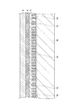
図1は、本実施形態に係る半導体レーザ素子1の光導波方向に垂直な断面を示す図である。図2は、図1のII−II線に沿った断面図である。半導体レーザ素子1は、n型InP基板2、n型InPクラッド層3、活性層4、p型InPクラッド層5、p型InPブロック層6、n型InPブロック層7、p型InP層8、コンタクト層9、保護膜10、p型電極11、及び、n型電極12を備えている。
図16は、第2実施形態にかかる半導体レーザ素子20の断面図である。半導体レーザ素子20は、第1実施形態の半導体レーザ素子1の構成に加えて、変調領域21を更に備える。変調領域21は、第2回折格子15上に形成されており、光導波路22と、p型InPクラッド層5上に設けられたコンタクト層23と、コンタクト層23上に設けられたp型電極24とを有する。光導波路22は、量子井戸構造を有する半導体積層体である。なお、変調領域21内のn型InP基板2、p型InPクラッド層5及びn型電極12のそれぞれは、活性層4の上方又は下方に設けられたn型InP基板2、p型InPクラッド層5及びn型電極12の一部である。この半導体レーザ素子20では、p型電極24とn型電極12との間に変調電圧が印加されることにより、活性層4において発生したレーザ光が光導波路22を通過する際に変調される。なお、光導波路22は例えば以下の手法によって形成される。具体的には、最初に図8等に示される活性層4において、第2回折格子15上の該活性層4を選択的にエッチングする。そして、活性層4がエッチングされた領域に選択的に光導波路22となる積層体を形成する。光導波路22を形成した後の工程は、第1実施形態と同じである。本実施形態では変調領域21を形成するための導波路の製造方法を説明したが、変調領域21以外の用途の導波路の形成方法も、本実施形態と同様の方法で形成することができる。
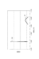
図17は、第3実施形態にかかる半導体レーザ素子の製造工程のうち、ウェハ16の上に回折格子を形成する工程において、ウェハ16の主面に垂直な方向からウェハ16を見た図である。図18は、図17に示すウェハ16のうち、半導体素子になるべき部分の1つを拡大した図である。
図20は、第4実施形態にかかる半導体レーザ素子の製造工程のうち、ウェハ16の上に回折格子を形成する工程において、ウェハ16の主面に垂直な方向からウェハ16を見た図である。図21は、図20に示すウェハ16のうち、後に半導体素子になる部分の1つを拡大した図である。
図23は、第5実施形態にかかる半導体レーザ素子の製造工程のうち、ウェハ16の上に回折格子を形成する工程において、ウェハ16の主面に垂直な方向からウェハ16を見た図である。図24は、図23に示すウェハ16のうち、後に半導体素子になる部分の1つを拡大した図である。
Claims (7)
- ウェハ上に回折格子層を形成する第1工程と、
前記回折格子層上に互いに周期の異なる第1レジストパターン及び第2レジストパターンを、電子ビーム露光法を用いて連続して形成する第2工程と、
前記第1レジストパターン及び前記第2レジストパターンをマスクとし、前記回折格子層をエッチングすることによって、互いに周期の異なる第1回折格子及び第2回折格子を形成する第3工程と、
前記第1回折格子上に利得を有する活性層、及び、前記第2回折格子上に利得を有さない導波路層を形成する第4工程と、
を含み、
前記第2工程では、前記第1レジストパターンの両側に前記第2レジストパターンを形成し、
前記第2回折格子の周期は、前記第1回折格子の周期の1.05倍以上もしくは0.95倍以下であり、
前記第2回折格子側に端面を形成する第5工程をさらに含む、半導体レーザ素子の製造方法。 - 前記ウェハを、前記第2回折格子が存する部分において劈開することにより、劈開面を形成する第5工程をさらに含む、請求項1に記載の半導体レーザ素子の製造方法。
- 前記第2工程では、
連続して設けられる前記第1回折格子及び前記第2回折格子を少なくとも一ずつ含む複数の被露光領域を、光導波方向に沿ってそれぞれ離間するように設定し、
前記複数の被露光領域のそれぞれに対して、前記電子ビームによって露光する、請求項1又は2に記載の半導体レーザ素子の製造方法。 - 前記第1回折格子、前記第2回折格子及び前記活性層を同一幅のストライプマスクを用いてエッチングすることにより、前記第1回折格子のストライプ幅以下のストライプ幅を有し、前記第1回折格子、前記第2回折格子、及び前記活性層を含むストライプ状のメサ部を形成する第6工程をさらに含み、
前記第6工程後、前記第1回折格子のストライプ幅は、前記第2回折格子のストライプ幅と同一である、請求項1〜3のいずれか一項に記載の半導体レーザ素子の製造方法。 - 第1の幅を有するストライプ状の前記第1回折格子と、前記第2回折格子と、前記活性層とをエッチングすることにより、前記第1の幅以下のストライプ幅を有するメサストライプ構造を形成する第6工程をさらに含み、
前記第1工程では、
連続して設けられる前記第1回折格子及び前記第2回折格子を少なくとも一ずつ含む複数の被露光領域を、光導波方向に沿ってそれぞれ連結するように設定し、
前記複数の被露光領域の連結部を前記第2回折格子に重ねるように設定し、
前記第2回折格子において前記連結部と重なる部分の幅は、前記第1の幅よりも大きい、請求項1〜3のいずれか一項に記載の半導体レーザ素子の製造方法。 - 基板上に形成される第1回折格子と、
前記第1回折格子の光導波方向における少なくとも片端に接続され、前記第1回折格子の周期の1.05倍以上又は0.95倍以下の周期を有する第2回折格子と、
前記第1回折格子の上に形成され、利得を有する活性層と、
前記第2回折格子の上に形成され、利得を有さない導波路層と、
を備え、
前記第2回折格子は、前記第1回折格子よりも端面側に配置される、半導体レーザ素子。 - 前記第2回折格子は、前記光導波方向において前記第1回折格子の両側に配置される、請求項6に記載の半導体レーザ素子。
Applications Claiming Priority (4)
| Application Number | Priority Date | Filing Date | Title |
|---|---|---|---|
| JP2014091042 | 2014-04-25 | ||
| JP2014091042 | 2014-04-25 | ||
| JP2015028474 | 2015-02-17 | ||
| JP2015028474 | 2015-02-17 |
Publications (3)
| Publication Number | Publication Date |
|---|---|
| JP2016154203A JP2016154203A (ja) | 2016-08-25 |
| JP2016154203A5 JP2016154203A5 (ja) | 2017-12-07 |
| JP6657537B2 true JP6657537B2 (ja) | 2020-03-04 |
Family
ID=54335655
Family Applications (1)
| Application Number | Title | Priority Date | Filing Date |
|---|---|---|---|
| JP2015088507A Active JP6657537B2 (ja) | 2014-04-25 | 2015-04-23 | 半導体レーザ素子及び半導体レーザ素子の製造方法 |
Country Status (2)
| Country | Link |
|---|---|
| US (1) | US9800021B2 (ja) |
| JP (1) | JP6657537B2 (ja) |
Families Citing this family (2)
| Publication number | Priority date | Publication date | Assignee | Title |
|---|---|---|---|---|
| JP6962515B2 (ja) * | 2017-09-07 | 2021-11-05 | 住友電工デバイス・イノベーション株式会社 | 半導体レーザ素子の製造方法 |
| JP7458885B2 (ja) | 2020-01-28 | 2024-04-01 | 日本ルメンタム株式会社 | 半導体光増幅器集積レーザ |
Family Cites Families (19)
| Publication number | Priority date | Publication date | Assignee | Title |
|---|---|---|---|---|
| JPS61190368A (ja) * | 1985-02-20 | 1986-08-25 | Matsushita Electric Ind Co Ltd | 微細パタ−ンの形成方法 |
| JPS62285418A (ja) * | 1986-06-03 | 1987-12-11 | Fujitsu Ltd | 微細幅パタ−ンの露光方法 |
| JP2527833B2 (ja) * | 1990-07-17 | 1996-08-28 | 三菱電機株式会社 | 回折格子の製造方法 |
| JPH0817262B2 (ja) * | 1989-08-18 | 1996-02-21 | 三菱電機株式会社 | 単一波長発振半導体レーザ装置 |
| JPH04100287A (ja) * | 1990-08-20 | 1992-04-02 | Hitachi Ltd | 半導体レーザ装置 |
| JPH0529703A (ja) | 1991-07-19 | 1993-02-05 | Toshiba Corp | 半導体レ−ザ素子 |
| JP3151755B2 (ja) * | 1993-04-26 | 2001-04-03 | 日本電信電話株式会社 | 分布帰還型半導体レーザ |
| JPH07128510A (ja) * | 1993-10-27 | 1995-05-19 | Canon Inc | 回折格子の作成方法 |
| JPH085849A (ja) * | 1994-06-20 | 1996-01-12 | Nippon Telegr & Teleph Corp <Ntt> | 導波路型光素子 |
| JP3180725B2 (ja) * | 1997-08-05 | 2001-06-25 | 日本電気株式会社 | 分布帰還型半導体レーザ |
| JP2950302B2 (ja) * | 1997-11-25 | 1999-09-20 | 日本電気株式会社 | 半導体レーザ |
| WO2001065648A2 (en) * | 2000-03-03 | 2001-09-07 | Optium, Inc. | Self-pulsing multi-section complex-coupled distributed feedback (dfb) laser |
| JP2002050569A (ja) * | 2000-08-02 | 2002-02-15 | Hitachi Ltd | パターン形成方法 |
| JP2007088285A (ja) * | 2005-09-22 | 2007-04-05 | Nec Electronics Corp | 半導体レーザ素子の製造方法および半導体レーザ素子 |
| JP4552894B2 (ja) * | 2006-05-12 | 2010-09-29 | 住友電気工業株式会社 | 分布帰還型半導体レーザを作製する方法 |
| JP5326810B2 (ja) * | 2009-05-22 | 2013-10-30 | 住友電気工業株式会社 | 半導体光素子を作製する方法 |
| JP5646852B2 (ja) * | 2010-01-08 | 2014-12-24 | 日本オクラロ株式会社 | 半導体光素子及びその製造方法 |
| JP5589908B2 (ja) * | 2011-03-11 | 2014-09-17 | 三菱電機株式会社 | 分布帰還型半導体レーザの製造方法 |
| JP2011176374A (ja) * | 2011-06-13 | 2011-09-08 | Fujitsu Ltd | 半導体レーザ及び半導体光集積素子 |
-
2015
- 2015-04-23 JP JP2015088507A patent/JP6657537B2/ja active Active
- 2015-04-24 US US14/696,102 patent/US9800021B2/en active Active
Also Published As
| Publication number | Publication date |
|---|---|
| JP2016154203A (ja) | 2016-08-25 |
| US20150311674A1 (en) | 2015-10-29 |
| US9800021B2 (en) | 2017-10-24 |
Similar Documents
| Publication | Publication Date | Title |
|---|---|---|
| JP5177285B2 (ja) | 光素子及びその製造方法 | |
| JP5589908B2 (ja) | 分布帰還型半導体レーザの製造方法 | |
| JP2013149723A (ja) | 光集積素子の製造方法 | |
| US8637338B2 (en) | Method for producing integrated optical device | |
| TWI528671B (zh) | 半導體裝置之製造方法、半導體裝置以及半導體裝置之製造系統 | |
| JP6657537B2 (ja) | 半導体レーザ素子及び半導体レーザ素子の製造方法 | |
| JP6084428B2 (ja) | 半導体光集積素子及びその製造方法 | |
| US10903620B2 (en) | Semiconductor device, and method for manufacturing semiconductor device | |
| US10326257B2 (en) | Semiconductor laser device and manufacturing method of the same | |
| JP6962515B2 (ja) | 半導体レーザ素子の製造方法 | |
| JP6468180B2 (ja) | 光半導体装置の製造方法 | |
| JP6270387B2 (ja) | 半導体光共振器、半導体光素子及び光通信モジュール | |
| JP2003234540A (ja) | 分布帰還型レーザ装置、半導体光装置および分布帰還型レーザ装置の製造方法 | |
| JP2010278278A (ja) | 光半導体装置 | |
| CN111903020B (zh) | 半导体装置的制造方法 | |
| JPH08162706A (ja) | 集積化半導体光素子の製造方法 | |
| JP2009260192A (ja) | 半導体光集積素子及びその製造方法 | |
| JP5277877B2 (ja) | 光導波路素子の製造方法 | |
| JP5786425B2 (ja) | 光集積素子の製造方法 | |
| JP6499268B2 (ja) | 半導体光素子及び光通信モジュール | |
| JP2009064838A (ja) | 光半導体素子及びその製造方法 | |
| JPH0642583B2 (ja) | 半導体レーザ装置 | |
| JP5445272B2 (ja) | 光半導体素子の製造方法 | |
| JP5418359B2 (ja) | 分布帰還型半導体レーザ | |
| JPH1056231A (ja) | 半導体レーザ素子の製造方法および半導体レーザ素子 |
Legal Events
| Date | Code | Title | Description |
|---|---|---|---|
| A521 | Request for written amendment filed |
Free format text: JAPANESE INTERMEDIATE CODE: A523 Effective date: 20171024 |
|
| A621 | Written request for application examination |
Free format text: JAPANESE INTERMEDIATE CODE: A621 Effective date: 20171024 |
|
| A977 | Report on retrieval |
Free format text: JAPANESE INTERMEDIATE CODE: A971007 Effective date: 20180913 |
|
| A131 | Notification of reasons for refusal |
Free format text: JAPANESE INTERMEDIATE CODE: A131 Effective date: 20181002 |
|
| A521 | Request for written amendment filed |
Free format text: JAPANESE INTERMEDIATE CODE: A523 Effective date: 20181119 |
|
| A131 | Notification of reasons for refusal |
Free format text: JAPANESE INTERMEDIATE CODE: A131 Effective date: 20190507 |
|
| A521 | Request for written amendment filed |
Free format text: JAPANESE INTERMEDIATE CODE: A523 Effective date: 20190705 |
|
| TRDD | Decision of grant or rejection written | ||
| A01 | Written decision to grant a patent or to grant a registration (utility model) |
Free format text: JAPANESE INTERMEDIATE CODE: A01 Effective date: 20200107 |
|
| A61 | First payment of annual fees (during grant procedure) |
Free format text: JAPANESE INTERMEDIATE CODE: A61 Effective date: 20200117 |
|
| R150 | Certificate of patent or registration of utility model |
Ref document number: 6657537 Country of ref document: JP Free format text: JAPANESE INTERMEDIATE CODE: R150 |
|
| R250 | Receipt of annual fees |
Free format text: JAPANESE INTERMEDIATE CODE: R250 |
|
| R250 | Receipt of annual fees |
Free format text: JAPANESE INTERMEDIATE CODE: R250 |