JP6652451B2 - 半導体装置およびその製造方法 - Google Patents
半導体装置およびその製造方法 Download PDFInfo
- Publication number
- JP6652451B2 JP6652451B2 JP2016117617A JP2016117617A JP6652451B2 JP 6652451 B2 JP6652451 B2 JP 6652451B2 JP 2016117617 A JP2016117617 A JP 2016117617A JP 2016117617 A JP2016117617 A JP 2016117617A JP 6652451 B2 JP6652451 B2 JP 6652451B2
- Authority
- JP
- Japan
- Prior art keywords
- film
- gate electrode
- region
- semiconductor device
- insulating film
- Prior art date
- Legal status (The legal status is an assumption and is not a legal conclusion. Google has not performed a legal analysis and makes no representation as to the accuracy of the status listed.)
- Active
Links
- 239000004065 semiconductor Substances 0.000 title claims description 300
- 238000004519 manufacturing process Methods 0.000 title claims description 70
- 230000015654 memory Effects 0.000 claims description 203
- 229910021332 silicide Inorganic materials 0.000 claims description 135
- FVBUAEGBCNSCDD-UHFFFAOYSA-N silicide(4-) Chemical compound [Si-4] FVBUAEGBCNSCDD-UHFFFAOYSA-N 0.000 claims description 135
- 229910052751 metal Inorganic materials 0.000 claims description 121
- 239000002184 metal Substances 0.000 claims description 121
- 239000000758 substrate Substances 0.000 claims description 81
- 238000000034 method Methods 0.000 claims description 60
- 238000002955 isolation Methods 0.000 claims description 37
- 238000010438 heat treatment Methods 0.000 claims description 26
- 238000004544 sputter deposition Methods 0.000 claims description 25
- 239000010936 titanium Substances 0.000 claims description 19
- 238000003860 storage Methods 0.000 claims description 18
- 230000015572 biosynthetic process Effects 0.000 claims description 11
- RTAQQCXQSZGOHL-UHFFFAOYSA-N Titanium Chemical compound [Ti] RTAQQCXQSZGOHL-UHFFFAOYSA-N 0.000 claims description 10
- 229910052719 titanium Inorganic materials 0.000 claims description 10
- 230000000149 penetrating effect Effects 0.000 claims description 6
- 229910021334 nickel silicide Inorganic materials 0.000 claims description 4
- RUFLMLWJRZAWLJ-UHFFFAOYSA-N nickel silicide Chemical compound [Ni]=[Si]=[Ni] RUFLMLWJRZAWLJ-UHFFFAOYSA-N 0.000 claims description 4
- 229910021341 titanium silicide Inorganic materials 0.000 claims description 4
- 230000001681 protective effect Effects 0.000 claims description 3
- 238000006243 chemical reaction Methods 0.000 claims description 2
- 239000010410 layer Substances 0.000 description 210
- 239000011229 interlayer Substances 0.000 description 42
- VYPSYNLAJGMNEJ-UHFFFAOYSA-N Silicium dioxide Chemical compound O=[Si]=O VYPSYNLAJGMNEJ-UHFFFAOYSA-N 0.000 description 32
- 229910052814 silicon oxide Inorganic materials 0.000 description 32
- 238000009792 diffusion process Methods 0.000 description 30
- 229910052581 Si3N4 Inorganic materials 0.000 description 29
- HQVNEWCFYHHQES-UHFFFAOYSA-N silicon nitride Chemical compound N12[Si]34N5[Si]62N3[Si]51N64 HQVNEWCFYHHQES-UHFFFAOYSA-N 0.000 description 29
- 238000005229 chemical vapour deposition Methods 0.000 description 26
- 229920002120 photoresistant polymer Polymers 0.000 description 26
- 239000012535 impurity Substances 0.000 description 15
- 238000005530 etching Methods 0.000 description 14
- XUIMIQQOPSSXEZ-UHFFFAOYSA-N Silicon Chemical compound [Si] XUIMIQQOPSSXEZ-UHFFFAOYSA-N 0.000 description 9
- 238000001312 dry etching Methods 0.000 description 9
- 238000002347 injection Methods 0.000 description 9
- 239000007924 injection Substances 0.000 description 9
- 229910052710 silicon Inorganic materials 0.000 description 9
- 239000010703 silicon Substances 0.000 description 9
- NRTOMJZYCJJWKI-UHFFFAOYSA-N Titanium nitride Chemical compound [Ti]#N NRTOMJZYCJJWKI-UHFFFAOYSA-N 0.000 description 8
- 239000004020 conductor Substances 0.000 description 8
- 238000005468 ion implantation Methods 0.000 description 8
- PXHVJJICTQNCMI-UHFFFAOYSA-N nickel Substances [Ni] PXHVJJICTQNCMI-UHFFFAOYSA-N 0.000 description 6
- BASFCYQUMIYNBI-UHFFFAOYSA-N platinum Substances [Pt] BASFCYQUMIYNBI-UHFFFAOYSA-N 0.000 description 6
- 230000004888 barrier function Effects 0.000 description 5
- 239000002784 hot electron Substances 0.000 description 5
- MZLGASXMSKOWSE-UHFFFAOYSA-N tantalum nitride Chemical compound [Ta]#N MZLGASXMSKOWSE-UHFFFAOYSA-N 0.000 description 5
- WFKWXMTUELFFGS-UHFFFAOYSA-N tungsten Chemical compound [W] WFKWXMTUELFFGS-UHFFFAOYSA-N 0.000 description 5
- 229910052721 tungsten Inorganic materials 0.000 description 5
- 239000010937 tungsten Substances 0.000 description 5
- ZOXJGFHDIHLPTG-UHFFFAOYSA-N Boron Chemical compound [B] ZOXJGFHDIHLPTG-UHFFFAOYSA-N 0.000 description 4
- 229910005883 NiSi Inorganic materials 0.000 description 4
- OAICVXFJPJFONN-UHFFFAOYSA-N Phosphorus Chemical compound [P] OAICVXFJPJFONN-UHFFFAOYSA-N 0.000 description 4
- 229910000577 Silicon-germanium Inorganic materials 0.000 description 4
- UQZIWOQVLUASCR-UHFFFAOYSA-N alumane;titanium Chemical compound [AlH3].[Ti] UQZIWOQVLUASCR-UHFFFAOYSA-N 0.000 description 4
- 229910052782 aluminium Inorganic materials 0.000 description 4
- XAGFODPZIPBFFR-UHFFFAOYSA-N aluminium Chemical compound [Al] XAGFODPZIPBFFR-UHFFFAOYSA-N 0.000 description 4
- 229910052785 arsenic Inorganic materials 0.000 description 4
- RQNWIZPPADIBDY-UHFFFAOYSA-N arsenic atom Chemical compound [As] RQNWIZPPADIBDY-UHFFFAOYSA-N 0.000 description 4
- 229910052796 boron Inorganic materials 0.000 description 4
- 230000000052 comparative effect Effects 0.000 description 4
- 238000010586 diagram Methods 0.000 description 4
- 230000000694 effects Effects 0.000 description 4
- 239000000463 material Substances 0.000 description 4
- NFFIWVVINABMKP-UHFFFAOYSA-N methylidynetantalum Chemical compound [Ta]#C NFFIWVVINABMKP-UHFFFAOYSA-N 0.000 description 4
- 229910052698 phosphorus Inorganic materials 0.000 description 4
- 239000011574 phosphorus Substances 0.000 description 4
- 238000000206 photolithography Methods 0.000 description 4
- 238000004151 rapid thermal annealing Methods 0.000 description 4
- 229910010271 silicon carbide Inorganic materials 0.000 description 4
- HBMJWWWQQXIZIP-UHFFFAOYSA-N silicon carbide Chemical compound [Si+]#[C-] HBMJWWWQQXIZIP-UHFFFAOYSA-N 0.000 description 4
- 229910003468 tantalcarbide Inorganic materials 0.000 description 4
- MTPVUVINMAGMJL-UHFFFAOYSA-N trimethyl(1,1,2,2,2-pentafluoroethyl)silane Chemical compound C[Si](C)(C)C(F)(F)C(F)(F)F MTPVUVINMAGMJL-UHFFFAOYSA-N 0.000 description 4
- UONOETXJSWQNOL-UHFFFAOYSA-N tungsten carbide Chemical compound [W+]#[C-] UONOETXJSWQNOL-UHFFFAOYSA-N 0.000 description 4
- 238000001039 wet etching Methods 0.000 description 4
- QNRATNLHPGXHMA-XZHTYLCXSA-N (r)-(6-ethoxyquinolin-4-yl)-[(2s,4s,5r)-5-ethyl-1-azabicyclo[2.2.2]octan-2-yl]methanol;hydrochloride Chemical compound Cl.C([C@H]([C@H](C1)CC)C2)CN1[C@@H]2[C@H](O)C1=CC=NC2=CC=C(OCC)C=C21 QNRATNLHPGXHMA-XZHTYLCXSA-N 0.000 description 3
- 229910008484 TiSi Inorganic materials 0.000 description 3
- 230000007423 decrease Effects 0.000 description 3
- 230000005669 field effect Effects 0.000 description 3
- 230000003647 oxidation Effects 0.000 description 3
- 238000007254 oxidation reaction Methods 0.000 description 3
- TWNQGVIAIRXVLR-UHFFFAOYSA-N oxo(oxoalumanyloxy)alumane Chemical compound O=[Al]O[Al]=O TWNQGVIAIRXVLR-UHFFFAOYSA-N 0.000 description 3
- 229910021420 polycrystalline silicon Inorganic materials 0.000 description 3
- 229920005591 polysilicon Polymers 0.000 description 3
- 229910052715 tantalum Inorganic materials 0.000 description 3
- GUVRBAGPIYLISA-UHFFFAOYSA-N tantalum atom Chemical compound [Ta] GUVRBAGPIYLISA-UHFFFAOYSA-N 0.000 description 3
- ITWBWJFEJCHKSN-UHFFFAOYSA-N 1,4,7-triazonane Chemical compound C1CNCCNCCN1 ITWBWJFEJCHKSN-UHFFFAOYSA-N 0.000 description 2
- LEVVHYCKPQWKOP-UHFFFAOYSA-N [Si].[Ge] Chemical compound [Si].[Ge] LEVVHYCKPQWKOP-UHFFFAOYSA-N 0.000 description 2
- 230000002159 abnormal effect Effects 0.000 description 2
- IVHJCRXBQPGLOV-UHFFFAOYSA-N azanylidynetungsten Chemical compound [W]#N IVHJCRXBQPGLOV-UHFFFAOYSA-N 0.000 description 2
- 239000000872 buffer Substances 0.000 description 2
- 230000002542 deteriorative effect Effects 0.000 description 2
- 230000006870 function Effects 0.000 description 2
- 229910000449 hafnium oxide Inorganic materials 0.000 description 2
- WIHZLLGSGQNAGK-UHFFFAOYSA-N hafnium(4+);oxygen(2-) Chemical compound [O-2].[O-2].[Hf+4] WIHZLLGSGQNAGK-UHFFFAOYSA-N 0.000 description 2
- 239000011810 insulating material Substances 0.000 description 2
- MRELNEQAGSRDBK-UHFFFAOYSA-N lanthanum(3+);oxygen(2-) Chemical compound [O-2].[O-2].[O-2].[La+3].[La+3] MRELNEQAGSRDBK-UHFFFAOYSA-N 0.000 description 2
- 150000004767 nitrides Chemical class 0.000 description 2
- 230000001590 oxidative effect Effects 0.000 description 2
- 229910052697 platinum Inorganic materials 0.000 description 2
- 238000005498 polishing Methods 0.000 description 2
- 230000003068 static effect Effects 0.000 description 2
- 239000000126 substance Substances 0.000 description 2
- RYGMFSIKBFXOCR-UHFFFAOYSA-N Copper Chemical compound [Cu] RYGMFSIKBFXOCR-UHFFFAOYSA-N 0.000 description 1
- 229910004129 HfSiO Inorganic materials 0.000 description 1
- -1 Metal Oxide Nitride Chemical class 0.000 description 1
- 238000013459 approach Methods 0.000 description 1
- 238000004140 cleaning Methods 0.000 description 1
- 229910052802 copper Inorganic materials 0.000 description 1
- 239000010949 copper Substances 0.000 description 1
- 230000005684 electric field Effects 0.000 description 1
- 238000009413 insulation Methods 0.000 description 1
- 239000012212 insulator Substances 0.000 description 1
- 239000011159 matrix material Substances 0.000 description 1
- 229910044991 metal oxide Inorganic materials 0.000 description 1
- 239000000203 mixture Substances 0.000 description 1
- 229910021421 monocrystalline silicon Inorganic materials 0.000 description 1
- 229910052759 nickel Inorganic materials 0.000 description 1
- 230000010355 oscillation Effects 0.000 description 1
- BPUBBGLMJRNUCC-UHFFFAOYSA-N oxygen(2-);tantalum(5+) Chemical compound [O-2].[O-2].[O-2].[O-2].[O-2].[Ta+5].[Ta+5] BPUBBGLMJRNUCC-UHFFFAOYSA-N 0.000 description 1
- RVTZCBVAJQQJTK-UHFFFAOYSA-N oxygen(2-);zirconium(4+) Chemical compound [O-2].[O-2].[Zr+4] RVTZCBVAJQQJTK-UHFFFAOYSA-N 0.000 description 1
- 238000007517 polishing process Methods 0.000 description 1
- 238000007781 pre-processing Methods 0.000 description 1
- 239000000243 solution Substances 0.000 description 1
- 125000006850 spacer group Chemical group 0.000 description 1
- 229910001936 tantalum oxide Inorganic materials 0.000 description 1
- 230000005641 tunneling Effects 0.000 description 1
- 229910001928 zirconium oxide Inorganic materials 0.000 description 1
Images


Classifications
-
- H—ELECTRICITY
- H01—ELECTRIC ELEMENTS
- H01L—SEMICONDUCTOR DEVICES NOT COVERED BY CLASS H10
- H01L29/00—Semiconductor devices adapted for rectifying, amplifying, oscillating or switching, or capacitors or resistors with at least one potential-jump barrier or surface barrier, e.g. PN junction depletion layer or carrier concentration layer; Details of semiconductor bodies or of electrodes thereof ; Multistep manufacturing processes therefor
- H01L29/66—Types of semiconductor device ; Multistep manufacturing processes therefor
- H01L29/68—Types of semiconductor device ; Multistep manufacturing processes therefor controllable by only the electric current supplied, or only the electric potential applied, to an electrode which does not carry the current to be rectified, amplified or switched
- H01L29/76—Unipolar devices, e.g. field effect transistors
- H01L29/772—Field effect transistors
- H01L29/78—Field effect transistors with field effect produced by an insulated gate
- H01L29/785—Field effect transistors with field effect produced by an insulated gate having a channel with a horizontal current flow in a vertical sidewall of a semiconductor body, e.g. FinFET, MuGFET
-
- H—ELECTRICITY
- H10—SEMICONDUCTOR DEVICES; ELECTRIC SOLID-STATE DEVICES NOT OTHERWISE PROVIDED FOR
- H10B—ELECTRONIC MEMORY DEVICES
- H10B43/00—EEPROM devices comprising charge-trapping gate insulators
- H10B43/30—EEPROM devices comprising charge-trapping gate insulators characterised by the memory core region
-
- H—ELECTRICITY
- H01—ELECTRIC ELEMENTS
- H01L—SEMICONDUCTOR DEVICES NOT COVERED BY CLASS H10
- H01L21/00—Processes or apparatus adapted for the manufacture or treatment of semiconductor or solid state devices or of parts thereof
- H01L21/02—Manufacture or treatment of semiconductor devices or of parts thereof
- H01L21/04—Manufacture or treatment of semiconductor devices or of parts thereof the devices having at least one potential-jump barrier or surface barrier, e.g. PN junction, depletion layer or carrier concentration layer
- H01L21/18—Manufacture or treatment of semiconductor devices or of parts thereof the devices having at least one potential-jump barrier or surface barrier, e.g. PN junction, depletion layer or carrier concentration layer the devices having semiconductor bodies comprising elements of Group IV of the Periodic System or AIIIBV compounds with or without impurities, e.g. doping materials
- H01L21/28—Manufacture of electrodes on semiconductor bodies using processes or apparatus not provided for in groups H01L21/20 - H01L21/268
- H01L21/283—Deposition of conductive or insulating materials for electrodes conducting electric current
- H01L21/285—Deposition of conductive or insulating materials for electrodes conducting electric current from a gas or vapour, e.g. condensation
- H01L21/28506—Deposition of conductive or insulating materials for electrodes conducting electric current from a gas or vapour, e.g. condensation of conductive layers
- H01L21/28512—Deposition of conductive or insulating materials for electrodes conducting electric current from a gas or vapour, e.g. condensation of conductive layers on semiconductor bodies comprising elements of Group IV of the Periodic System
- H01L21/2855—Deposition of conductive or insulating materials for electrodes conducting electric current from a gas or vapour, e.g. condensation of conductive layers on semiconductor bodies comprising elements of Group IV of the Periodic System by physical means, e.g. sputtering, evaporation
-
- H—ELECTRICITY
- H01—ELECTRIC ELEMENTS
- H01L—SEMICONDUCTOR DEVICES NOT COVERED BY CLASS H10
- H01L21/00—Processes or apparatus adapted for the manufacture or treatment of semiconductor or solid state devices or of parts thereof
- H01L21/02—Manufacture or treatment of semiconductor devices or of parts thereof
- H01L21/04—Manufacture or treatment of semiconductor devices or of parts thereof the devices having at least one potential-jump barrier or surface barrier, e.g. PN junction, depletion layer or carrier concentration layer
- H01L21/18—Manufacture or treatment of semiconductor devices or of parts thereof the devices having at least one potential-jump barrier or surface barrier, e.g. PN junction, depletion layer or carrier concentration layer the devices having semiconductor bodies comprising elements of Group IV of the Periodic System or AIIIBV compounds with or without impurities, e.g. doping materials
- H01L21/30—Treatment of semiconductor bodies using processes or apparatus not provided for in groups H01L21/20 - H01L21/26
- H01L21/324—Thermal treatment for modifying the properties of semiconductor bodies, e.g. annealing, sintering
-
- H—ELECTRICITY
- H01—ELECTRIC ELEMENTS
- H01L—SEMICONDUCTOR DEVICES NOT COVERED BY CLASS H10
- H01L21/00—Processes or apparatus adapted for the manufacture or treatment of semiconductor or solid state devices or of parts thereof
- H01L21/67—Apparatus specially adapted for handling semiconductor or electric solid state devices during manufacture or treatment thereof; Apparatus specially adapted for handling wafers during manufacture or treatment of semiconductor or electric solid state devices or components ; Apparatus not specifically provided for elsewhere
- H01L21/67005—Apparatus not specifically provided for elsewhere
- H01L21/67011—Apparatus for manufacture or treatment
- H01L21/67155—Apparatus for manufacturing or treating in a plurality of work-stations
- H01L21/67161—Apparatus for manufacturing or treating in a plurality of work-stations characterized by the layout of the process chambers
- H01L21/67167—Apparatus for manufacturing or treating in a plurality of work-stations characterized by the layout of the process chambers surrounding a central transfer chamber
-
- H—ELECTRICITY
- H01—ELECTRIC ELEMENTS
- H01L—SEMICONDUCTOR DEVICES NOT COVERED BY CLASS H10
- H01L21/00—Processes or apparatus adapted for the manufacture or treatment of semiconductor or solid state devices or of parts thereof
- H01L21/70—Manufacture or treatment of devices consisting of a plurality of solid state components formed in or on a common substrate or of parts thereof; Manufacture of integrated circuit devices or of parts thereof
- H01L21/71—Manufacture of specific parts of devices defined in group H01L21/70
- H01L21/76—Making of isolation regions between components
- H01L21/762—Dielectric regions, e.g. EPIC dielectric isolation, LOCOS; Trench refilling techniques, SOI technology, use of channel stoppers
- H01L21/76224—Dielectric regions, e.g. EPIC dielectric isolation, LOCOS; Trench refilling techniques, SOI technology, use of channel stoppers using trench refilling with dielectric materials
-
- H—ELECTRICITY
- H01—ELECTRIC ELEMENTS
- H01L—SEMICONDUCTOR DEVICES NOT COVERED BY CLASS H10
- H01L21/00—Processes or apparatus adapted for the manufacture or treatment of semiconductor or solid state devices or of parts thereof
- H01L21/70—Manufacture or treatment of devices consisting of a plurality of solid state components formed in or on a common substrate or of parts thereof; Manufacture of integrated circuit devices or of parts thereof
- H01L21/77—Manufacture or treatment of devices consisting of a plurality of solid state components or integrated circuits formed in, or on, a common substrate
- H01L21/78—Manufacture or treatment of devices consisting of a plurality of solid state components or integrated circuits formed in, or on, a common substrate with subsequent division of the substrate into plural individual devices
- H01L21/82—Manufacture or treatment of devices consisting of a plurality of solid state components or integrated circuits formed in, or on, a common substrate with subsequent division of the substrate into plural individual devices to produce devices, e.g. integrated circuits, each consisting of a plurality of components
- H01L21/822—Manufacture or treatment of devices consisting of a plurality of solid state components or integrated circuits formed in, or on, a common substrate with subsequent division of the substrate into plural individual devices to produce devices, e.g. integrated circuits, each consisting of a plurality of components the substrate being a semiconductor, using silicon technology
- H01L21/8232—Field-effect technology
- H01L21/8234—MIS technology, i.e. integration processes of field effect transistors of the conductor-insulator-semiconductor type
- H01L21/823431—MIS technology, i.e. integration processes of field effect transistors of the conductor-insulator-semiconductor type with a particular manufacturing method of transistors with a horizontal current flow in a vertical sidewall of a semiconductor body, e.g. FinFET, MuGFET
-
- H—ELECTRICITY
- H01—ELECTRIC ELEMENTS
- H01L—SEMICONDUCTOR DEVICES NOT COVERED BY CLASS H10
- H01L27/00—Devices consisting of a plurality of semiconductor or other solid-state components formed in or on a common substrate
- H01L27/02—Devices consisting of a plurality of semiconductor or other solid-state components formed in or on a common substrate including semiconductor components specially adapted for rectifying, oscillating, amplifying or switching and having at least one potential-jump barrier or surface barrier; including integrated passive circuit elements with at least one potential-jump barrier or surface barrier
- H01L27/04—Devices consisting of a plurality of semiconductor or other solid-state components formed in or on a common substrate including semiconductor components specially adapted for rectifying, oscillating, amplifying or switching and having at least one potential-jump barrier or surface barrier; including integrated passive circuit elements with at least one potential-jump barrier or surface barrier the substrate being a semiconductor body
- H01L27/08—Devices consisting of a plurality of semiconductor or other solid-state components formed in or on a common substrate including semiconductor components specially adapted for rectifying, oscillating, amplifying or switching and having at least one potential-jump barrier or surface barrier; including integrated passive circuit elements with at least one potential-jump barrier or surface barrier the substrate being a semiconductor body including only semiconductor components of a single kind
- H01L27/085—Devices consisting of a plurality of semiconductor or other solid-state components formed in or on a common substrate including semiconductor components specially adapted for rectifying, oscillating, amplifying or switching and having at least one potential-jump barrier or surface barrier; including integrated passive circuit elements with at least one potential-jump barrier or surface barrier the substrate being a semiconductor body including only semiconductor components of a single kind including field-effect components only
- H01L27/088—Devices consisting of a plurality of semiconductor or other solid-state components formed in or on a common substrate including semiconductor components specially adapted for rectifying, oscillating, amplifying or switching and having at least one potential-jump barrier or surface barrier; including integrated passive circuit elements with at least one potential-jump barrier or surface barrier the substrate being a semiconductor body including only semiconductor components of a single kind including field-effect components only the components being field-effect transistors with insulated gate
- H01L27/0886—Devices consisting of a plurality of semiconductor or other solid-state components formed in or on a common substrate including semiconductor components specially adapted for rectifying, oscillating, amplifying or switching and having at least one potential-jump barrier or surface barrier; including integrated passive circuit elements with at least one potential-jump barrier or surface barrier the substrate being a semiconductor body including only semiconductor components of a single kind including field-effect components only the components being field-effect transistors with insulated gate including transistors with a horizontal current flow in a vertical sidewall of a semiconductor body, e.g. FinFET, MuGFET
-
- H—ELECTRICITY
- H01—ELECTRIC ELEMENTS
- H01L—SEMICONDUCTOR DEVICES NOT COVERED BY CLASS H10
- H01L29/00—Semiconductor devices adapted for rectifying, amplifying, oscillating or switching, or capacitors or resistors with at least one potential-jump barrier or surface barrier, e.g. PN junction depletion layer or carrier concentration layer; Details of semiconductor bodies or of electrodes thereof ; Multistep manufacturing processes therefor
- H01L29/02—Semiconductor bodies ; Multistep manufacturing processes therefor
- H01L29/06—Semiconductor bodies ; Multistep manufacturing processes therefor characterised by their shape; characterised by the shapes, relative sizes, or dispositions of the semiconductor regions ; characterised by the concentration or distribution of impurities within semiconductor regions
- H01L29/0603—Semiconductor bodies ; Multistep manufacturing processes therefor characterised by their shape; characterised by the shapes, relative sizes, or dispositions of the semiconductor regions ; characterised by the concentration or distribution of impurities within semiconductor regions characterised by particular constructional design considerations, e.g. for preventing surface leakage, for controlling electric field concentration or for internal isolations regions
- H01L29/0642—Isolation within the component, i.e. internal isolation
- H01L29/0649—Dielectric regions, e.g. SiO2 regions, air gaps
-
- H—ELECTRICITY
- H01—ELECTRIC ELEMENTS
- H01L—SEMICONDUCTOR DEVICES NOT COVERED BY CLASS H10
- H01L29/00—Semiconductor devices adapted for rectifying, amplifying, oscillating or switching, or capacitors or resistors with at least one potential-jump barrier or surface barrier, e.g. PN junction depletion layer or carrier concentration layer; Details of semiconductor bodies or of electrodes thereof ; Multistep manufacturing processes therefor
- H01L29/02—Semiconductor bodies ; Multistep manufacturing processes therefor
- H01L29/06—Semiconductor bodies ; Multistep manufacturing processes therefor characterised by their shape; characterised by the shapes, relative sizes, or dispositions of the semiconductor regions ; characterised by the concentration or distribution of impurities within semiconductor regions
- H01L29/08—Semiconductor bodies ; Multistep manufacturing processes therefor characterised by their shape; characterised by the shapes, relative sizes, or dispositions of the semiconductor regions ; characterised by the concentration or distribution of impurities within semiconductor regions with semiconductor regions connected to an electrode carrying current to be rectified, amplified or switched and such electrode being part of a semiconductor device which comprises three or more electrodes
- H01L29/0843—Source or drain regions of field-effect devices
- H01L29/0847—Source or drain regions of field-effect devices of field-effect transistors with insulated gate
-
- H—ELECTRICITY
- H01—ELECTRIC ELEMENTS
- H01L—SEMICONDUCTOR DEVICES NOT COVERED BY CLASS H10
- H01L29/00—Semiconductor devices adapted for rectifying, amplifying, oscillating or switching, or capacitors or resistors with at least one potential-jump barrier or surface barrier, e.g. PN junction depletion layer or carrier concentration layer; Details of semiconductor bodies or of electrodes thereof ; Multistep manufacturing processes therefor
- H01L29/02—Semiconductor bodies ; Multistep manufacturing processes therefor
- H01L29/06—Semiconductor bodies ; Multistep manufacturing processes therefor characterised by their shape; characterised by the shapes, relative sizes, or dispositions of the semiconductor regions ; characterised by the concentration or distribution of impurities within semiconductor regions
- H01L29/10—Semiconductor bodies ; Multistep manufacturing processes therefor characterised by their shape; characterised by the shapes, relative sizes, or dispositions of the semiconductor regions ; characterised by the concentration or distribution of impurities within semiconductor regions with semiconductor regions connected to an electrode not carrying current to be rectified, amplified or switched and such electrode being part of a semiconductor device which comprises three or more electrodes
- H01L29/1025—Channel region of field-effect devices
- H01L29/1029—Channel region of field-effect devices of field-effect transistors
- H01L29/1033—Channel region of field-effect devices of field-effect transistors with insulated gate, e.g. characterised by the length, the width, the geometric contour or the doping structure
- H01L29/1037—Channel region of field-effect devices of field-effect transistors with insulated gate, e.g. characterised by the length, the width, the geometric contour or the doping structure and non-planar channel
-
- H—ELECTRICITY
- H01—ELECTRIC ELEMENTS
- H01L—SEMICONDUCTOR DEVICES NOT COVERED BY CLASS H10
- H01L29/00—Semiconductor devices adapted for rectifying, amplifying, oscillating or switching, or capacitors or resistors with at least one potential-jump barrier or surface barrier, e.g. PN junction depletion layer or carrier concentration layer; Details of semiconductor bodies or of electrodes thereof ; Multistep manufacturing processes therefor
- H01L29/40—Electrodes ; Multistep manufacturing processes therefor
- H01L29/401—Multistep manufacturing processes
- H01L29/4011—Multistep manufacturing processes for data storage electrodes
- H01L29/40117—Multistep manufacturing processes for data storage electrodes the electrodes comprising a charge-trapping insulator
-
- H—ELECTRICITY
- H01—ELECTRIC ELEMENTS
- H01L—SEMICONDUCTOR DEVICES NOT COVERED BY CLASS H10
- H01L29/00—Semiconductor devices adapted for rectifying, amplifying, oscillating or switching, or capacitors or resistors with at least one potential-jump barrier or surface barrier, e.g. PN junction depletion layer or carrier concentration layer; Details of semiconductor bodies or of electrodes thereof ; Multistep manufacturing processes therefor
- H01L29/40—Electrodes ; Multistep manufacturing processes therefor
- H01L29/41—Electrodes ; Multistep manufacturing processes therefor characterised by their shape, relative sizes or dispositions
- H01L29/423—Electrodes ; Multistep manufacturing processes therefor characterised by their shape, relative sizes or dispositions not carrying the current to be rectified, amplified or switched
- H01L29/42312—Gate electrodes for field effect devices
- H01L29/42316—Gate electrodes for field effect devices for field-effect transistors
- H01L29/4232—Gate electrodes for field effect devices for field-effect transistors with insulated gate
- H01L29/4234—Gate electrodes for transistors with charge trapping gate insulator
- H01L29/42344—Gate electrodes for transistors with charge trapping gate insulator with at least one additional gate, e.g. program gate, erase gate or select gate
-
- H—ELECTRICITY
- H01—ELECTRIC ELEMENTS
- H01L—SEMICONDUCTOR DEVICES NOT COVERED BY CLASS H10
- H01L29/00—Semiconductor devices adapted for rectifying, amplifying, oscillating or switching, or capacitors or resistors with at least one potential-jump barrier or surface barrier, e.g. PN junction depletion layer or carrier concentration layer; Details of semiconductor bodies or of electrodes thereof ; Multistep manufacturing processes therefor
- H01L29/40—Electrodes ; Multistep manufacturing processes therefor
- H01L29/43—Electrodes ; Multistep manufacturing processes therefor characterised by the materials of which they are formed
- H01L29/45—Ohmic electrodes
-
- H—ELECTRICITY
- H01—ELECTRIC ELEMENTS
- H01L—SEMICONDUCTOR DEVICES NOT COVERED BY CLASS H10
- H01L29/00—Semiconductor devices adapted for rectifying, amplifying, oscillating or switching, or capacitors or resistors with at least one potential-jump barrier or surface barrier, e.g. PN junction depletion layer or carrier concentration layer; Details of semiconductor bodies or of electrodes thereof ; Multistep manufacturing processes therefor
- H01L29/40—Electrodes ; Multistep manufacturing processes therefor
- H01L29/43—Electrodes ; Multistep manufacturing processes therefor characterised by the materials of which they are formed
- H01L29/49—Metal-insulator-semiconductor electrodes, e.g. gates of MOSFET
- H01L29/495—Metal-insulator-semiconductor electrodes, e.g. gates of MOSFET the conductor material next to the insulator being a simple metal, e.g. W, Mo
-
- H—ELECTRICITY
- H01—ELECTRIC ELEMENTS
- H01L—SEMICONDUCTOR DEVICES NOT COVERED BY CLASS H10
- H01L29/00—Semiconductor devices adapted for rectifying, amplifying, oscillating or switching, or capacitors or resistors with at least one potential-jump barrier or surface barrier, e.g. PN junction depletion layer or carrier concentration layer; Details of semiconductor bodies or of electrodes thereof ; Multistep manufacturing processes therefor
- H01L29/40—Electrodes ; Multistep manufacturing processes therefor
- H01L29/43—Electrodes ; Multistep manufacturing processes therefor characterised by the materials of which they are formed
- H01L29/49—Metal-insulator-semiconductor electrodes, e.g. gates of MOSFET
- H01L29/4966—Metal-insulator-semiconductor electrodes, e.g. gates of MOSFET the conductor material next to the insulator being a composite material, e.g. organic material, TiN, MoSi2
-
- H—ELECTRICITY
- H01—ELECTRIC ELEMENTS
- H01L—SEMICONDUCTOR DEVICES NOT COVERED BY CLASS H10
- H01L29/00—Semiconductor devices adapted for rectifying, amplifying, oscillating or switching, or capacitors or resistors with at least one potential-jump barrier or surface barrier, e.g. PN junction depletion layer or carrier concentration layer; Details of semiconductor bodies or of electrodes thereof ; Multistep manufacturing processes therefor
- H01L29/66—Types of semiconductor device ; Multistep manufacturing processes therefor
- H01L29/66007—Multistep manufacturing processes
- H01L29/66075—Multistep manufacturing processes of devices having semiconductor bodies comprising group 14 or group 13/15 materials
- H01L29/66227—Multistep manufacturing processes of devices having semiconductor bodies comprising group 14 or group 13/15 materials the devices being controllable only by the electric current supplied or the electric potential applied, to an electrode which does not carry the current to be rectified, amplified or switched, e.g. three-terminal devices
- H01L29/66409—Unipolar field-effect transistors
- H01L29/66477—Unipolar field-effect transistors with an insulated gate, i.e. MISFET
- H01L29/665—Unipolar field-effect transistors with an insulated gate, i.e. MISFET using self aligned silicidation, i.e. salicide
-
- H—ELECTRICITY
- H01—ELECTRIC ELEMENTS
- H01L—SEMICONDUCTOR DEVICES NOT COVERED BY CLASS H10
- H01L29/00—Semiconductor devices adapted for rectifying, amplifying, oscillating or switching, or capacitors or resistors with at least one potential-jump barrier or surface barrier, e.g. PN junction depletion layer or carrier concentration layer; Details of semiconductor bodies or of electrodes thereof ; Multistep manufacturing processes therefor
- H01L29/66—Types of semiconductor device ; Multistep manufacturing processes therefor
- H01L29/66007—Multistep manufacturing processes
- H01L29/66075—Multistep manufacturing processes of devices having semiconductor bodies comprising group 14 or group 13/15 materials
- H01L29/66227—Multistep manufacturing processes of devices having semiconductor bodies comprising group 14 or group 13/15 materials the devices being controllable only by the electric current supplied or the electric potential applied, to an electrode which does not carry the current to be rectified, amplified or switched, e.g. three-terminal devices
- H01L29/66409—Unipolar field-effect transistors
- H01L29/66477—Unipolar field-effect transistors with an insulated gate, i.e. MISFET
- H01L29/66545—Unipolar field-effect transistors with an insulated gate, i.e. MISFET using a dummy, i.e. replacement gate in a process wherein at least a part of the final gate is self aligned to the dummy gate
-
- H—ELECTRICITY
- H01—ELECTRIC ELEMENTS
- H01L—SEMICONDUCTOR DEVICES NOT COVERED BY CLASS H10
- H01L29/00—Semiconductor devices adapted for rectifying, amplifying, oscillating or switching, or capacitors or resistors with at least one potential-jump barrier or surface barrier, e.g. PN junction depletion layer or carrier concentration layer; Details of semiconductor bodies or of electrodes thereof ; Multistep manufacturing processes therefor
- H01L29/66—Types of semiconductor device ; Multistep manufacturing processes therefor
- H01L29/66007—Multistep manufacturing processes
- H01L29/66075—Multistep manufacturing processes of devices having semiconductor bodies comprising group 14 or group 13/15 materials
- H01L29/66227—Multistep manufacturing processes of devices having semiconductor bodies comprising group 14 or group 13/15 materials the devices being controllable only by the electric current supplied or the electric potential applied, to an electrode which does not carry the current to be rectified, amplified or switched, e.g. three-terminal devices
- H01L29/66409—Unipolar field-effect transistors
- H01L29/66477—Unipolar field-effect transistors with an insulated gate, i.e. MISFET
- H01L29/66787—Unipolar field-effect transistors with an insulated gate, i.e. MISFET with a gate at the side of the channel
- H01L29/66795—Unipolar field-effect transistors with an insulated gate, i.e. MISFET with a gate at the side of the channel with a horizontal current flow in a vertical sidewall of a semiconductor body, e.g. FinFET, MuGFET
-
- H—ELECTRICITY
- H01—ELECTRIC ELEMENTS
- H01L—SEMICONDUCTOR DEVICES NOT COVERED BY CLASS H10
- H01L29/00—Semiconductor devices adapted for rectifying, amplifying, oscillating or switching, or capacitors or resistors with at least one potential-jump barrier or surface barrier, e.g. PN junction depletion layer or carrier concentration layer; Details of semiconductor bodies or of electrodes thereof ; Multistep manufacturing processes therefor
- H01L29/66—Types of semiconductor device ; Multistep manufacturing processes therefor
- H01L29/66007—Multistep manufacturing processes
- H01L29/66075—Multistep manufacturing processes of devices having semiconductor bodies comprising group 14 or group 13/15 materials
- H01L29/66227—Multistep manufacturing processes of devices having semiconductor bodies comprising group 14 or group 13/15 materials the devices being controllable only by the electric current supplied or the electric potential applied, to an electrode which does not carry the current to be rectified, amplified or switched, e.g. three-terminal devices
- H01L29/66409—Unipolar field-effect transistors
- H01L29/66477—Unipolar field-effect transistors with an insulated gate, i.e. MISFET
- H01L29/66833—Unipolar field-effect transistors with an insulated gate, i.e. MISFET with a charge trapping gate insulator, e.g. MNOS transistors
-
- H—ELECTRICITY
- H01—ELECTRIC ELEMENTS
- H01L—SEMICONDUCTOR DEVICES NOT COVERED BY CLASS H10
- H01L29/00—Semiconductor devices adapted for rectifying, amplifying, oscillating or switching, or capacitors or resistors with at least one potential-jump barrier or surface barrier, e.g. PN junction depletion layer or carrier concentration layer; Details of semiconductor bodies or of electrodes thereof ; Multistep manufacturing processes therefor
- H01L29/66—Types of semiconductor device ; Multistep manufacturing processes therefor
- H01L29/68—Types of semiconductor device ; Multistep manufacturing processes therefor controllable by only the electric current supplied, or only the electric potential applied, to an electrode which does not carry the current to be rectified, amplified or switched
- H01L29/76—Unipolar devices, e.g. field effect transistors
- H01L29/772—Field effect transistors
- H01L29/78—Field effect transistors with field effect produced by an insulated gate
- H01L29/785—Field effect transistors with field effect produced by an insulated gate having a channel with a horizontal current flow in a vertical sidewall of a semiconductor body, e.g. FinFET, MuGFET
- H01L29/7851—Field effect transistors with field effect produced by an insulated gate having a channel with a horizontal current flow in a vertical sidewall of a semiconductor body, e.g. FinFET, MuGFET with the body tied to the substrate
-
- H—ELECTRICITY
- H01—ELECTRIC ELEMENTS
- H01L—SEMICONDUCTOR DEVICES NOT COVERED BY CLASS H10
- H01L29/00—Semiconductor devices adapted for rectifying, amplifying, oscillating or switching, or capacitors or resistors with at least one potential-jump barrier or surface barrier, e.g. PN junction depletion layer or carrier concentration layer; Details of semiconductor bodies or of electrodes thereof ; Multistep manufacturing processes therefor
- H01L29/66—Types of semiconductor device ; Multistep manufacturing processes therefor
- H01L29/68—Types of semiconductor device ; Multistep manufacturing processes therefor controllable by only the electric current supplied, or only the electric potential applied, to an electrode which does not carry the current to be rectified, amplified or switched
- H01L29/76—Unipolar devices, e.g. field effect transistors
- H01L29/772—Field effect transistors
- H01L29/78—Field effect transistors with field effect produced by an insulated gate
- H01L29/792—Field effect transistors with field effect produced by an insulated gate with charge trapping gate insulator, e.g. MNOS-memory transistors
-
- H—ELECTRICITY
- H10—SEMICONDUCTOR DEVICES; ELECTRIC SOLID-STATE DEVICES NOT OTHERWISE PROVIDED FOR
- H10B—ELECTRONIC MEMORY DEVICES
- H10B43/00—EEPROM devices comprising charge-trapping gate insulators
- H10B43/40—EEPROM devices comprising charge-trapping gate insulators characterised by the peripheral circuit region
Description
<半導体チップのレイアウト構成例>
本実施の形態における不揮発性メモリを有する半導体装置について図面を参照しながら説明する。まず、不揮発性メモリを含むシステムが形成された半導体装置(半導体チップ)のレイアウト構成について説明する。図1は、本実施の形態における半導体チップCHPのレイアウト構成例を示す概略図である。図1において、半導体チップCHPは、CPU(Central Processing Unit)CC1、RAM(Random Access Memory)CC2、アナログ回路CC3を有している。また、半導体チップCHPは、EEPROM(Electrically Erasable Programmable Read Only Memory)CC4、フラッシュメモリCC5およびI/O(Input/Output)回路CC6を有し、半導体装置を構成している。
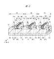
以下に、図2〜図5を用いて、本実施の形態の半導体装置の構造について説明する。図2は、本実施の形態における半導体装置の平面図である。図3は、本実施の形態における半導体装置の斜視図である。図4および図5は、本実施の形態における半導体装置の断面図である。なお、図3、図5では、ウェルの図示を省略する。また、図5では、ソース・ドレイン領域の図示を省略する。
nMIS領域1BおよびpMIS領域1Cに形成されたエピタキシャル層EP1、EP2のそれぞれの上面であって、シリサイド層S3を介してプラグPG2に接続された面の位置は、シリサイド層S1の上面であって、プラグPG1に接続された面の位置よりも高い。これは、フィンFA上に形成されたシリサイド層S1の膜厚よりも、フィンFB上またはフィンFC上に形成されたエピタキシャル層EP1、EP2のそれぞれの膜厚の方が大きいためである。
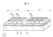
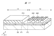
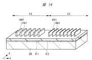
以下に、図6〜図53を用いて、本実施の形態の半導体装置の製造方法について説明する。図6、図8、図10、図12、図15、図17、図19、図20〜図40および図42〜図53は、本実施の形態の半導体装置の形成工程中の断面図である。図7、図9、図11、図13、図14、図16および図18は、本実施の形態の半導体装置の形成工程中の斜視図である。図41は、本実施の形態の半導体装置の形成工程に用いるスパッタリング装置の模式的な平面図である。図8、図10、図12、図15、図17および図19は、図7、図9、図11、図14、図16および図18の同じ位置におけるY方向に沿う断面を示す図である。上記斜視図、図42および図44では、ウェルの図示を省略する。
次に、不揮発性メモリの動作例について、図54および図55を参照して説明する。
次に、本実施の形態の半導体装置の製造方法の主要な特徴および効果について、比較例として図58を用いて説明する。図58は、比較例の半導体装置の製造工程中の断面図であって、図42に示す断面図に対応する。
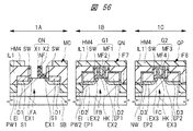
以下に、図56および図57を用いて、本実施の形態2の半導体装置の製造方法について説明する。図56および図57は、本実施の形態2の半導体装置の形成工程中の断面図である。なお、図57では図を分かりやすくするため、図56に示す積層膜である絶縁膜ONを1つの膜として示している。
1B nMIS領域
1C pMIS領域
CG 制御ゲート電極
D1〜D3 拡散領域
EI 素子分離膜
EX1〜EX3 エクステンション領域
FA〜FC フィン
G1、G2 ゲート電極
GF ゲート絶縁膜
MC メモリセル
MG メモリゲート電極
ON 絶縁膜(ONO膜)
QN n型トランジスタ
QP p型トランジスタ
S1〜S3、SS シリサイド層
SB 半導体基板
Claims (15)
- 主面に沿って並ぶ第1領域および第2領域を有する半導体基板と、
前記第1領域の前記半導体基板の一部分であって、前記半導体基板の上面から突出し、前記半導体基板の前記主面に沿う第1方向に延在する第1突出部と、
前記第1突出部の上面上に第1絶縁膜を介して形成され、前記第1方向に直交する第2方向に延在する第1ゲート電極と、
前記第1突出部の前記上面上に電荷蓄積部である第2絶縁膜を介して形成され、前記第1ゲート電極の一方の側壁に前記第2絶縁膜を介して隣接し、前記第2方向に延在する第2ゲート電極と、
前記第1ゲート電極および前記第2ゲート電極からなるパターンを前記第1方向において挟むように前記第1突出部の前記上面に形成された第1ソース・ドレイン領域と、
前記第2領域の前記半導体基板の一部分であって、前記半導体基板の前記上面から突出し、前記第1方向に延在する第2突出部と、
前記第2突出部の上面上に第3絶縁膜を介して形成され、前記第2方向に延在する第3ゲート電極と、
前記第3ゲート電極を前記第1方向において挟むように前記第2突出部の前記上面に形成された第2ソース・ドレイン領域と、
前記第1ソース・ドレイン領域のそれぞれの上面および側壁を覆い、前記第1突出部に接する第1シリサイド層と、
前記第2ソース・ドレイン領域のそれぞれの上面および側壁を覆い、前記第2突出部に接する半導体層と、
を有し、
前記第1ゲート電極、前記第2ゲート電極および前記第1ソース・ドレイン領域は、不揮発性記憶素子を構成し、
前記第3ゲート電極および前記第2ソース・ドレイン領域は、トランジスタを構成する、半導体装置。 - 請求項1記載の半導体装置において、
前記半導体層の上面の位置は、前記第1シリサイド層の上面の位置よりも高い、半導体装置。 - 請求項1記載の半導体装置において、
前記半導体基板上に形成され、前記不揮発性記憶素子および前記トランジスタを覆う第4絶縁膜と、
前記第4絶縁膜を貫通し、前記第1シリサイド層を介して、前記第1ソース・ドレイン領域に電気的に接続された第1接続部と、
前記第4絶縁膜を貫通し、前記第2ソース・ドレイン領域に電気的に接続された第2接続部と、
をさらに有し、
前記第2接続部の底面の位置は、前記第1接続部の底面の位置よりも高い、半導体装置。 - 請求項3記載の半導体装置において、
前記第1接続部と前記第1シリサイド層とは、互いに接しており、
前記第2接続部は、前記第2接続部および前記半導体層の間に形成された第2シリサイド層と前記半導体層とを介して前記第2突出部内の前記第2ソース・ドレイン領域に接続されている、半導体装置。 - 請求項4記載の半導体装置において、
前記第2接続部の横の前記半導体層の前記上面は、前記第2シリサイド層から露出している、半導体装置。 - 請求項4記載の半導体装置において、
前記第1シリサイド層は、ニッケルシリサイドからなり、前記第2シリサイド層は、チタンシリサイドからなる、半導体装置。 - 請求項3記載の半導体装置において、
前記第1接続部と前記第1シリサイド層との間には、チタンを含む第1金属膜が介在しており、
前記第2接続部は、前記第2接続部および前記半導体層の間に形成された第2シリサイド層と前記半導体層とを介して前記第2突出部内の前記第2ソース・ドレイン領域に接続されている、半導体装置。 - 請求項1記載の半導体装置において、
前記半導体層は、前記第2ソース・ドレイン領域の一部を構成している、半導体装置。 - 請求項1記載の半導体装置において、
前記第3ゲート電極は、第2金属膜を含む、半導体装置。 - 請求項1記載の半導体装置において、
前記第1ゲート電極は、第3金属膜を含み、前記第2ゲート電極は、第4金属膜を含む、半導体装置。 - (a)半導体基板を準備する工程、
(b)前記半導体基板の上面の一部を後退させることで、前記半導体基板の一部分であって、前記半導体基板の前記上面から突出し、前記半導体基板の前記上面に沿う第1方向に延在する第1突出部と、前記半導体基板の前記上面から突出し、前記第1方向に延在する第2突出部とを形成する工程、
(c)前記第1突出部および前記第2突出部の間の溝内を埋め込む素子分離膜を形成する工程、
(d)前記(c)工程の後、前記第1突出部の直上に第1絶縁膜を介して第1ゲート電極を形成し、前記第1ゲート電極の一方の側壁に電荷蓄積部である第2絶縁膜を介して隣接する領域の前記第1突出部の直上に前記第2絶縁膜を介して第2ゲート電極を形成し、前記第2突出部の直上に第3絶縁膜を介して第3ゲート電極を形成する工程、
(e)前記第3ゲート電極の横の前記第2突出部の上面および側壁を覆うエピタキシャル層を形成する工程、
(f)前記第3ゲート電極の横の前記第2突出部の上面に第2ソース・ドレイン領域を形成する工程、
(g)前記第1ゲート電極および前記第2ゲート電極からなるパターンの横の前記第1突出部の上面に第1ソース・ドレイン領域を形成する工程、
(h)前記(g)工程の後、前記第2突出部を保護膜により覆った状態で、前記パターンの横の前記第1ソース・ドレイン領域のそれぞれの上面および側壁を覆う第1シリサイド層を形成する工程、
を有し、
前記第1ゲート電極、前記第2ゲート電極および前記第1ソース・ドレイン領域は、不揮発性記憶素子を構成し、
前記第3ゲート電極および前記第2ソース・ドレイン領域は、トランジスタを構成する、半導体装置の製造方法。 - 請求項11記載の半導体装置の製造方法において、
前記エピタキシャル層の上面の位置は、前記第1シリサイド層の上面の位置よりも高い、半導体装置の製造方法。 - 請求項11記載の半導体装置の製造方法において、
前記(h)工程は、
(h1)前記第2突出部を保護膜により覆う工程、
(h2)前記(h1)工程の後、第1熱処理を行って前記第1突出部を加熱した状態で、前記第1突出部を覆う金属膜を形成することで、前記金属膜と前記第1突出部の表面とを反応させ、これにより前記金属膜と前記第1突出部の表面との間に第3シリサイド層を形成する工程、
(h3)前記(h2)工程の後、第2熱処理を行うことで、前記金属膜と前記第1突出部の表面とを反応させ、これにより前記第1シリサイド層を形成する工程、
を有する、半導体装置の製造方法。 - 請求項13記載の半導体装置の製造方法において、
前記(h2)工程では、前記第1突出部の側壁を覆う前記金属膜は、前記側壁に沿う方向において互いに離間して並ぶ複数の膜からなる、半導体装置の製造方法。 - 請求項13記載の半導体装置の製造方法において、
前記(h2)工程は、
(h4)熱処理用チャンバ内で前記第1熱処理を行う工程、
(h5)前記(h4)工程の後、前記半導体基板を、前記熱処理用チャンバ内から成膜用チャンバ内まで真空状態が維持された経路を通って搬送する工程、
(h6)前記(h5)工程の後、前記成膜用チャンバ内でスパッタリング法により前記金属膜の形成を行う工程、
を有する、半導体装置の製造方法。
Priority Applications (5)
| Application Number | Priority Date | Filing Date | Title |
|---|---|---|---|
| JP2016117617A JP6652451B2 (ja) | 2016-06-14 | 2016-06-14 | 半導体装置およびその製造方法 |
| US15/482,239 US9899403B2 (en) | 2016-06-14 | 2017-04-07 | Semiconductor device and method of manufacturing the same |
| CN201710356508.9A CN107507864B (zh) | 2016-06-14 | 2017-05-19 | 半导体器件及其制造方法 |
| TW106118450A TW201810677A (zh) | 2016-06-14 | 2017-06-05 | 半導體裝置及其製造方法 |
| US15/879,257 US10229925B2 (en) | 2016-06-14 | 2018-01-24 | Semiconductor device and method of manufacturing the same |
Applications Claiming Priority (1)
| Application Number | Priority Date | Filing Date | Title |
|---|---|---|---|
| JP2016117617A JP6652451B2 (ja) | 2016-06-14 | 2016-06-14 | 半導体装置およびその製造方法 |
Publications (3)
| Publication Number | Publication Date |
|---|---|
| JP2017224666A JP2017224666A (ja) | 2017-12-21 |
| JP2017224666A5 JP2017224666A5 (ja) | 2018-12-27 |
| JP6652451B2 true JP6652451B2 (ja) | 2020-02-26 |
Family
ID=60574221
Family Applications (1)
| Application Number | Title | Priority Date | Filing Date |
|---|---|---|---|
| JP2016117617A Active JP6652451B2 (ja) | 2016-06-14 | 2016-06-14 | 半導体装置およびその製造方法 |
Country Status (4)
| Country | Link |
|---|---|
| US (2) | US9899403B2 (ja) |
| JP (1) | JP6652451B2 (ja) |
| CN (1) | CN107507864B (ja) |
| TW (1) | TW201810677A (ja) |
Families Citing this family (16)
| Publication number | Priority date | Publication date | Assignee | Title |
|---|---|---|---|---|
| US10163901B1 (en) * | 2017-06-23 | 2018-12-25 | Globalfoundries Singapore Pte. Ltd. | Method and device for embedding flash memory and logic integration in FinFET technology |
| JP2019117913A (ja) * | 2017-12-27 | 2019-07-18 | ルネサスエレクトロニクス株式会社 | 半導体装置およびその製造方法 |
| JP6920192B2 (ja) * | 2017-12-28 | 2021-08-18 | ルネサスエレクトロニクス株式会社 | 半導体装置およびその製造方法 |
| US10515954B2 (en) | 2018-03-18 | 2019-12-24 | Taiwan Semiconductor Manufacturing Co., Ltd. | Semiconductor device having fin structures of varying dimensions |
| US10312247B1 (en) * | 2018-03-22 | 2019-06-04 | Silicon Storage Technology, Inc. | Two transistor FinFET-based split gate non-volatile floating gate flash memory and method of fabrication |
| JP6998267B2 (ja) * | 2018-05-08 | 2022-01-18 | ルネサスエレクトロニクス株式会社 | 半導体装置およびその製造方法 |
| JP7053388B2 (ja) * | 2018-06-28 | 2022-04-12 | ルネサスエレクトロニクス株式会社 | 半導体装置の製造方法 |
| CN110828460B (zh) * | 2018-08-14 | 2022-07-19 | 中芯国际集成电路制造(北京)有限公司 | 半导体器件及其形成方法 |
| CN110828380B (zh) * | 2018-08-14 | 2022-06-17 | 中芯国际集成电路制造(上海)有限公司 | 静态存储单元的形成方法及静态存储单元 |
| US11195923B2 (en) * | 2018-12-21 | 2021-12-07 | Applied Materials, Inc. | Method of fabricating a semiconductor device having reduced contact resistance |
| JP7232081B2 (ja) * | 2019-03-01 | 2023-03-02 | ルネサスエレクトロニクス株式会社 | 半導体装置およびその製造方法 |
| JP7200054B2 (ja) * | 2019-06-24 | 2023-01-06 | ルネサスエレクトロニクス株式会社 | 半導体装置およびその製造方法 |
| JP2021027096A (ja) * | 2019-08-01 | 2021-02-22 | ルネサスエレクトロニクス株式会社 | 半導体装置の製造方法 |
| KR102624201B1 (ko) * | 2019-09-06 | 2024-01-15 | 에스케이하이닉스 주식회사 | 저항 변화 메모리층을 구비하는 비휘발성 메모리 장치 |
| CN112490128A (zh) * | 2019-09-12 | 2021-03-12 | 中芯国际集成电路制造(上海)有限公司 | 半导体器件及其形成方法 |
| US20220051905A1 (en) * | 2020-08-12 | 2022-02-17 | Tokyo Electron Limited | Formation of low-temperature and high-temperature in-situ doped source and drain epitaxy using selective heating for wrap-around contact and vertically stacked device architectures |
Family Cites Families (24)
| Publication number | Priority date | Publication date | Assignee | Title |
|---|---|---|---|---|
| US7335945B2 (en) * | 2003-12-26 | 2008-02-26 | Electronics And Telecommunications Research Institute | Multi-gate MOS transistor and method of manufacturing the same |
| KR100532353B1 (ko) * | 2004-03-11 | 2005-11-30 | 삼성전자주식회사 | 핀 전계 효과 트랜지스터 및 그 제조방법 |
| JP2006041354A (ja) | 2004-07-29 | 2006-02-09 | Renesas Technology Corp | 半導体装置及びその製造方法 |
| JP2006066564A (ja) * | 2004-08-26 | 2006-03-09 | Renesas Technology Corp | 半導体装置およびその製造方法 |
| KR100672826B1 (ko) * | 2004-12-03 | 2007-01-22 | 삼성전자주식회사 | 핀 전계 효과 트랜지스터 및 그 제조방법 |
| KR100645065B1 (ko) * | 2005-06-23 | 2006-11-10 | 삼성전자주식회사 | 핀 전계 효과 트랜지스터와 이를 구비하는 비휘발성 메모리장치 및 그 형성 방법 |
| JP4921755B2 (ja) * | 2005-09-16 | 2012-04-25 | 株式会社東芝 | 半導体装置 |
| JP4791868B2 (ja) * | 2006-03-28 | 2011-10-12 | 株式会社東芝 | Fin−NAND型フラッシュメモリ |
| KR100745766B1 (ko) * | 2006-06-23 | 2007-08-02 | 삼성전자주식회사 | 네 개의 스토리지 노드막을 구비하는 비휘발성 메모리 소자및 그 동작 방법 |
| US8068370B2 (en) * | 2008-04-18 | 2011-11-29 | Macronix International Co., Ltd. | Floating gate memory device with interpoly charge trapping structure |
| JP5305969B2 (ja) * | 2009-02-17 | 2013-10-02 | 株式会社東芝 | 半導体装置 |
| US20110001169A1 (en) | 2009-07-01 | 2011-01-06 | International Business Machines Corporation | Forming uniform silicide on 3d structures |
| JP5538975B2 (ja) | 2010-03-29 | 2014-07-02 | ルネサスエレクトロニクス株式会社 | 半導体装置の製造方法 |
| JP2012234885A (ja) * | 2011-04-28 | 2012-11-29 | Toshiba Corp | 半導体装置及びその製造方法 |
| US9129827B2 (en) * | 2012-04-13 | 2015-09-08 | Intel Corporation | Conversion of strain-inducing buffer to electrical insulator |
| US8716803B2 (en) * | 2012-10-04 | 2014-05-06 | Flashsilicon Incorporation | 3-D single floating gate non-volatile memory device |
| US9299840B2 (en) * | 2013-03-08 | 2016-03-29 | Taiwan Semiconductor Manufacturing Company, Ltd. | FinFETs and methods for forming the same |
| US20150194433A1 (en) * | 2014-01-08 | 2015-07-09 | Broadcom Corporation | Gate substantial contact based one-time programmable device |
| JP2015185613A (ja) * | 2014-03-20 | 2015-10-22 | ルネサスエレクトロニクス株式会社 | 半導体装置およびその製造方法 |
| CN106030812B (zh) * | 2014-03-27 | 2019-09-24 | 英特尔公司 | 锗锡沟道晶体管 |
| CN106575672B (zh) * | 2014-09-19 | 2020-11-10 | 英特尔公司 | 创建具有富铟表面的砷化铟镓有源沟道的装置和方法 |
| KR102245133B1 (ko) * | 2014-10-13 | 2021-04-28 | 삼성전자 주식회사 | 이종 게이트 구조의 finFET를 구비한 반도체 소자 및 그 제조방법 |
| US10002876B2 (en) * | 2014-10-29 | 2018-06-19 | International Business Machines Corporation | FinFET vertical flash memory |
| KR102217246B1 (ko) * | 2014-11-12 | 2021-02-18 | 삼성전자주식회사 | 집적회로 소자 및 그 제조 방법 |
-
2016
- 2016-06-14 JP JP2016117617A patent/JP6652451B2/ja active Active
-
2017
- 2017-04-07 US US15/482,239 patent/US9899403B2/en active Active
- 2017-05-19 CN CN201710356508.9A patent/CN107507864B/zh active Active
- 2017-06-05 TW TW106118450A patent/TW201810677A/zh unknown
-
2018
- 2018-01-24 US US15/879,257 patent/US10229925B2/en active Active
Also Published As
| Publication number | Publication date |
|---|---|
| CN107507864B (zh) | 2022-09-20 |
| US9899403B2 (en) | 2018-02-20 |
| US20170358592A1 (en) | 2017-12-14 |
| CN107507864A (zh) | 2017-12-22 |
| US20180166459A1 (en) | 2018-06-14 |
| JP2017224666A (ja) | 2017-12-21 |
| TW201810677A (zh) | 2018-03-16 |
| US10229925B2 (en) | 2019-03-12 |
Similar Documents
| Publication | Publication Date | Title |
|---|---|---|
| JP6652451B2 (ja) | 半導体装置およびその製造方法 | |
| JP6750994B2 (ja) | 半導体装置およびその製造方法 | |
| US11393838B2 (en) | Semiconductor device and manufacturing method thereof | |
| JP2019121633A (ja) | 半導体装置およびその製造方法 | |
| JP6778607B2 (ja) | 半導体装置の製造方法 | |
| US9947679B2 (en) | Method of manufacturing semiconductor device with separately formed insulating films in main circuit and memory regions | |
| JP5707224B2 (ja) | 半導体装置およびその製造方法 | |
| US11133326B2 (en) | Semiconductor device and method of manufacturing thereof | |
| JP7200054B2 (ja) | 半導体装置およびその製造方法 | |
| JP6998267B2 (ja) | 半導体装置およびその製造方法 | |
| US11672121B2 (en) | Semiconductor memory device including separated epitaxial layers | |
| WO2016088196A1 (ja) | 半導体装置の製造方法および半導体装置 | |
| CN109494225B (zh) | 半导体器件及其制造方法 | |
| US10229998B2 (en) | Semiconductor device and method of manufacturing the same |
Legal Events
| Date | Code | Title | Description |
|---|---|---|---|
| A521 | Request for written amendment filed |
Free format text: JAPANESE INTERMEDIATE CODE: A523 Effective date: 20181116 |
|
| A621 | Written request for application examination |
Free format text: JAPANESE INTERMEDIATE CODE: A621 Effective date: 20181116 |
|
| A977 | Report on retrieval |
Free format text: JAPANESE INTERMEDIATE CODE: A971007 Effective date: 20190819 |
|
| A131 | Notification of reasons for refusal |
Free format text: JAPANESE INTERMEDIATE CODE: A131 Effective date: 20190903 |
|
| A521 | Request for written amendment filed |
Free format text: JAPANESE INTERMEDIATE CODE: A523 Effective date: 20191029 |
|
| TRDD | Decision of grant or rejection written | ||
| A01 | Written decision to grant a patent or to grant a registration (utility model) |
Free format text: JAPANESE INTERMEDIATE CODE: A01 Effective date: 20200107 |
|
| A61 | First payment of annual fees (during grant procedure) |
Free format text: JAPANESE INTERMEDIATE CODE: A61 Effective date: 20200123 |
|
| R150 | Certificate of patent or registration of utility model |
Ref document number: 6652451 Country of ref document: JP Free format text: JAPANESE INTERMEDIATE CODE: R150 |