JP6652451B2 - Semiconductor device and manufacturing method thereof - Google Patents
Semiconductor device and manufacturing method thereof Download PDFInfo
- Publication number
- JP6652451B2 JP6652451B2 JP2016117617A JP2016117617A JP6652451B2 JP 6652451 B2 JP6652451 B2 JP 6652451B2 JP 2016117617 A JP2016117617 A JP 2016117617A JP 2016117617 A JP2016117617 A JP 2016117617A JP 6652451 B2 JP6652451 B2 JP 6652451B2
- Authority
- JP
- Japan
- Prior art keywords
- film
- gate electrode
- region
- semiconductor device
- insulating film
- Prior art date
- Legal status (The legal status is an assumption and is not a legal conclusion. Google has not performed a legal analysis and makes no representation as to the accuracy of the status listed.)
- Active
Links
- 239000004065 semiconductor Substances 0.000 title claims description 300
- 238000004519 manufacturing process Methods 0.000 title claims description 70
- 230000015654 memory Effects 0.000 claims description 203
- 229910021332 silicide Inorganic materials 0.000 claims description 135
- FVBUAEGBCNSCDD-UHFFFAOYSA-N silicide(4-) Chemical compound [Si-4] FVBUAEGBCNSCDD-UHFFFAOYSA-N 0.000 claims description 135
- 229910052751 metal Inorganic materials 0.000 claims description 121
- 239000002184 metal Substances 0.000 claims description 121
- 239000000758 substrate Substances 0.000 claims description 81
- 238000000034 method Methods 0.000 claims description 60
- 238000002955 isolation Methods 0.000 claims description 37
- 238000010438 heat treatment Methods 0.000 claims description 26
- 238000004544 sputter deposition Methods 0.000 claims description 25
- 239000010936 titanium Substances 0.000 claims description 19
- 238000003860 storage Methods 0.000 claims description 18
- 230000015572 biosynthetic process Effects 0.000 claims description 11
- RTAQQCXQSZGOHL-UHFFFAOYSA-N Titanium Chemical compound [Ti] RTAQQCXQSZGOHL-UHFFFAOYSA-N 0.000 claims description 10
- 229910052719 titanium Inorganic materials 0.000 claims description 10
- 230000000149 penetrating effect Effects 0.000 claims description 6
- 229910021334 nickel silicide Inorganic materials 0.000 claims description 4
- RUFLMLWJRZAWLJ-UHFFFAOYSA-N nickel silicide Chemical compound [Ni]=[Si]=[Ni] RUFLMLWJRZAWLJ-UHFFFAOYSA-N 0.000 claims description 4
- 229910021341 titanium silicide Inorganic materials 0.000 claims description 4
- 230000001681 protective effect Effects 0.000 claims description 3
- 238000006243 chemical reaction Methods 0.000 claims description 2
- 239000010410 layer Substances 0.000 description 210
- 239000011229 interlayer Substances 0.000 description 42
- VYPSYNLAJGMNEJ-UHFFFAOYSA-N Silicium dioxide Chemical compound O=[Si]=O VYPSYNLAJGMNEJ-UHFFFAOYSA-N 0.000 description 32
- 229910052814 silicon oxide Inorganic materials 0.000 description 32
- 238000009792 diffusion process Methods 0.000 description 30
- 229910052581 Si3N4 Inorganic materials 0.000 description 29
- HQVNEWCFYHHQES-UHFFFAOYSA-N silicon nitride Chemical compound N12[Si]34N5[Si]62N3[Si]51N64 HQVNEWCFYHHQES-UHFFFAOYSA-N 0.000 description 29
- 238000005229 chemical vapour deposition Methods 0.000 description 26
- 229920002120 photoresistant polymer Polymers 0.000 description 26
- 239000012535 impurity Substances 0.000 description 15
- 238000005530 etching Methods 0.000 description 14
- XUIMIQQOPSSXEZ-UHFFFAOYSA-N Silicon Chemical compound [Si] XUIMIQQOPSSXEZ-UHFFFAOYSA-N 0.000 description 9
- 238000001312 dry etching Methods 0.000 description 9
- 238000002347 injection Methods 0.000 description 9
- 239000007924 injection Substances 0.000 description 9
- 229910052710 silicon Inorganic materials 0.000 description 9
- 239000010703 silicon Substances 0.000 description 9
- NRTOMJZYCJJWKI-UHFFFAOYSA-N Titanium nitride Chemical compound [Ti]#N NRTOMJZYCJJWKI-UHFFFAOYSA-N 0.000 description 8
- 239000004020 conductor Substances 0.000 description 8
- 238000005468 ion implantation Methods 0.000 description 8
- PXHVJJICTQNCMI-UHFFFAOYSA-N nickel Substances [Ni] PXHVJJICTQNCMI-UHFFFAOYSA-N 0.000 description 6
- BASFCYQUMIYNBI-UHFFFAOYSA-N platinum Substances [Pt] BASFCYQUMIYNBI-UHFFFAOYSA-N 0.000 description 6
- 230000004888 barrier function Effects 0.000 description 5
- 239000002784 hot electron Substances 0.000 description 5
- MZLGASXMSKOWSE-UHFFFAOYSA-N tantalum nitride Chemical compound [Ta]#N MZLGASXMSKOWSE-UHFFFAOYSA-N 0.000 description 5
- WFKWXMTUELFFGS-UHFFFAOYSA-N tungsten Chemical compound [W] WFKWXMTUELFFGS-UHFFFAOYSA-N 0.000 description 5
- 229910052721 tungsten Inorganic materials 0.000 description 5
- 239000010937 tungsten Substances 0.000 description 5
- ZOXJGFHDIHLPTG-UHFFFAOYSA-N Boron Chemical compound [B] ZOXJGFHDIHLPTG-UHFFFAOYSA-N 0.000 description 4
- 229910005883 NiSi Inorganic materials 0.000 description 4
- OAICVXFJPJFONN-UHFFFAOYSA-N Phosphorus Chemical compound [P] OAICVXFJPJFONN-UHFFFAOYSA-N 0.000 description 4
- 229910000577 Silicon-germanium Inorganic materials 0.000 description 4
- UQZIWOQVLUASCR-UHFFFAOYSA-N alumane;titanium Chemical compound [AlH3].[Ti] UQZIWOQVLUASCR-UHFFFAOYSA-N 0.000 description 4
- 229910052782 aluminium Inorganic materials 0.000 description 4
- XAGFODPZIPBFFR-UHFFFAOYSA-N aluminium Chemical compound [Al] XAGFODPZIPBFFR-UHFFFAOYSA-N 0.000 description 4
- 229910052785 arsenic Inorganic materials 0.000 description 4
- RQNWIZPPADIBDY-UHFFFAOYSA-N arsenic atom Chemical compound [As] RQNWIZPPADIBDY-UHFFFAOYSA-N 0.000 description 4
- 229910052796 boron Inorganic materials 0.000 description 4
- 230000000052 comparative effect Effects 0.000 description 4
- 238000010586 diagram Methods 0.000 description 4
- 230000000694 effects Effects 0.000 description 4
- 239000000463 material Substances 0.000 description 4
- NFFIWVVINABMKP-UHFFFAOYSA-N methylidynetantalum Chemical compound [Ta]#C NFFIWVVINABMKP-UHFFFAOYSA-N 0.000 description 4
- 229910052698 phosphorus Inorganic materials 0.000 description 4
- 239000011574 phosphorus Substances 0.000 description 4
- 238000000206 photolithography Methods 0.000 description 4
- 238000004151 rapid thermal annealing Methods 0.000 description 4
- 229910010271 silicon carbide Inorganic materials 0.000 description 4
- HBMJWWWQQXIZIP-UHFFFAOYSA-N silicon carbide Chemical compound [Si+]#[C-] HBMJWWWQQXIZIP-UHFFFAOYSA-N 0.000 description 4
- 229910003468 tantalcarbide Inorganic materials 0.000 description 4
- MTPVUVINMAGMJL-UHFFFAOYSA-N trimethyl(1,1,2,2,2-pentafluoroethyl)silane Chemical compound C[Si](C)(C)C(F)(F)C(F)(F)F MTPVUVINMAGMJL-UHFFFAOYSA-N 0.000 description 4
- UONOETXJSWQNOL-UHFFFAOYSA-N tungsten carbide Chemical compound [W+]#[C-] UONOETXJSWQNOL-UHFFFAOYSA-N 0.000 description 4
- 238000001039 wet etching Methods 0.000 description 4
- QNRATNLHPGXHMA-XZHTYLCXSA-N (r)-(6-ethoxyquinolin-4-yl)-[(2s,4s,5r)-5-ethyl-1-azabicyclo[2.2.2]octan-2-yl]methanol;hydrochloride Chemical compound Cl.C([C@H]([C@H](C1)CC)C2)CN1[C@@H]2[C@H](O)C1=CC=NC2=CC=C(OCC)C=C21 QNRATNLHPGXHMA-XZHTYLCXSA-N 0.000 description 3
- 229910008484 TiSi Inorganic materials 0.000 description 3
- 230000007423 decrease Effects 0.000 description 3
- 230000005669 field effect Effects 0.000 description 3
- 230000003647 oxidation Effects 0.000 description 3
- 238000007254 oxidation reaction Methods 0.000 description 3
- TWNQGVIAIRXVLR-UHFFFAOYSA-N oxo(oxoalumanyloxy)alumane Chemical compound O=[Al]O[Al]=O TWNQGVIAIRXVLR-UHFFFAOYSA-N 0.000 description 3
- 229910021420 polycrystalline silicon Inorganic materials 0.000 description 3
- 229920005591 polysilicon Polymers 0.000 description 3
- 229910052715 tantalum Inorganic materials 0.000 description 3
- GUVRBAGPIYLISA-UHFFFAOYSA-N tantalum atom Chemical compound [Ta] GUVRBAGPIYLISA-UHFFFAOYSA-N 0.000 description 3
- ITWBWJFEJCHKSN-UHFFFAOYSA-N 1,4,7-triazonane Chemical compound C1CNCCNCCN1 ITWBWJFEJCHKSN-UHFFFAOYSA-N 0.000 description 2
- LEVVHYCKPQWKOP-UHFFFAOYSA-N [Si].[Ge] Chemical compound [Si].[Ge] LEVVHYCKPQWKOP-UHFFFAOYSA-N 0.000 description 2
- 230000002159 abnormal effect Effects 0.000 description 2
- IVHJCRXBQPGLOV-UHFFFAOYSA-N azanylidynetungsten Chemical compound [W]#N IVHJCRXBQPGLOV-UHFFFAOYSA-N 0.000 description 2
- 239000000872 buffer Substances 0.000 description 2
- 230000002542 deteriorative effect Effects 0.000 description 2
- 230000006870 function Effects 0.000 description 2
- 229910000449 hafnium oxide Inorganic materials 0.000 description 2
- WIHZLLGSGQNAGK-UHFFFAOYSA-N hafnium(4+);oxygen(2-) Chemical compound [O-2].[O-2].[Hf+4] WIHZLLGSGQNAGK-UHFFFAOYSA-N 0.000 description 2
- 239000011810 insulating material Substances 0.000 description 2
- MRELNEQAGSRDBK-UHFFFAOYSA-N lanthanum(3+);oxygen(2-) Chemical compound [O-2].[O-2].[O-2].[La+3].[La+3] MRELNEQAGSRDBK-UHFFFAOYSA-N 0.000 description 2
- 150000004767 nitrides Chemical class 0.000 description 2
- 230000001590 oxidative effect Effects 0.000 description 2
- 229910052697 platinum Inorganic materials 0.000 description 2
- 238000005498 polishing Methods 0.000 description 2
- 230000003068 static effect Effects 0.000 description 2
- 239000000126 substance Substances 0.000 description 2
- RYGMFSIKBFXOCR-UHFFFAOYSA-N Copper Chemical compound [Cu] RYGMFSIKBFXOCR-UHFFFAOYSA-N 0.000 description 1
- 229910004129 HfSiO Inorganic materials 0.000 description 1
- -1 Metal Oxide Nitride Chemical class 0.000 description 1
- 238000013459 approach Methods 0.000 description 1
- 238000004140 cleaning Methods 0.000 description 1
- 229910052802 copper Inorganic materials 0.000 description 1
- 239000010949 copper Substances 0.000 description 1
- 230000005684 electric field Effects 0.000 description 1
- 238000009413 insulation Methods 0.000 description 1
- 239000012212 insulator Substances 0.000 description 1
- 239000011159 matrix material Substances 0.000 description 1
- 229910044991 metal oxide Inorganic materials 0.000 description 1
- 239000000203 mixture Substances 0.000 description 1
- 229910021421 monocrystalline silicon Inorganic materials 0.000 description 1
- 229910052759 nickel Inorganic materials 0.000 description 1
- 230000010355 oscillation Effects 0.000 description 1
- BPUBBGLMJRNUCC-UHFFFAOYSA-N oxygen(2-);tantalum(5+) Chemical compound [O-2].[O-2].[O-2].[O-2].[O-2].[Ta+5].[Ta+5] BPUBBGLMJRNUCC-UHFFFAOYSA-N 0.000 description 1
- RVTZCBVAJQQJTK-UHFFFAOYSA-N oxygen(2-);zirconium(4+) Chemical compound [O-2].[O-2].[Zr+4] RVTZCBVAJQQJTK-UHFFFAOYSA-N 0.000 description 1
- 238000007517 polishing process Methods 0.000 description 1
- 238000007781 pre-processing Methods 0.000 description 1
- 239000000243 solution Substances 0.000 description 1
- 125000006850 spacer group Chemical group 0.000 description 1
- 229910001936 tantalum oxide Inorganic materials 0.000 description 1
- 230000005641 tunneling Effects 0.000 description 1
- 229910001928 zirconium oxide Inorganic materials 0.000 description 1
Images


Classifications
-
- H—ELECTRICITY
- H01—ELECTRIC ELEMENTS
- H01L—SEMICONDUCTOR DEVICES NOT COVERED BY CLASS H10
- H01L29/00—Semiconductor devices adapted for rectifying, amplifying, oscillating or switching, or capacitors or resistors with at least one potential-jump barrier or surface barrier, e.g. PN junction depletion layer or carrier concentration layer; Details of semiconductor bodies or of electrodes thereof ; Multistep manufacturing processes therefor
- H01L29/66—Types of semiconductor device ; Multistep manufacturing processes therefor
- H01L29/68—Types of semiconductor device ; Multistep manufacturing processes therefor controllable by only the electric current supplied, or only the electric potential applied, to an electrode which does not carry the current to be rectified, amplified or switched
- H01L29/76—Unipolar devices, e.g. field effect transistors
- H01L29/772—Field effect transistors
- H01L29/78—Field effect transistors with field effect produced by an insulated gate
- H01L29/785—Field effect transistors with field effect produced by an insulated gate having a channel with a horizontal current flow in a vertical sidewall of a semiconductor body, e.g. FinFET, MuGFET
-
- H—ELECTRICITY
- H10—SEMICONDUCTOR DEVICES; ELECTRIC SOLID-STATE DEVICES NOT OTHERWISE PROVIDED FOR
- H10B—ELECTRONIC MEMORY DEVICES
- H10B43/00—EEPROM devices comprising charge-trapping gate insulators
- H10B43/30—EEPROM devices comprising charge-trapping gate insulators characterised by the memory core region
-
- H—ELECTRICITY
- H01—ELECTRIC ELEMENTS
- H01L—SEMICONDUCTOR DEVICES NOT COVERED BY CLASS H10
- H01L21/00—Processes or apparatus adapted for the manufacture or treatment of semiconductor or solid state devices or of parts thereof
- H01L21/02—Manufacture or treatment of semiconductor devices or of parts thereof
- H01L21/04—Manufacture or treatment of semiconductor devices or of parts thereof the devices having at least one potential-jump barrier or surface barrier, e.g. PN junction, depletion layer or carrier concentration layer
- H01L21/18—Manufacture or treatment of semiconductor devices or of parts thereof the devices having at least one potential-jump barrier or surface barrier, e.g. PN junction, depletion layer or carrier concentration layer the devices having semiconductor bodies comprising elements of Group IV of the Periodic System or AIIIBV compounds with or without impurities, e.g. doping materials
- H01L21/28—Manufacture of electrodes on semiconductor bodies using processes or apparatus not provided for in groups H01L21/20 - H01L21/268
- H01L21/283—Deposition of conductive or insulating materials for electrodes conducting electric current
- H01L21/285—Deposition of conductive or insulating materials for electrodes conducting electric current from a gas or vapour, e.g. condensation
- H01L21/28506—Deposition of conductive or insulating materials for electrodes conducting electric current from a gas or vapour, e.g. condensation of conductive layers
- H01L21/28512—Deposition of conductive or insulating materials for electrodes conducting electric current from a gas or vapour, e.g. condensation of conductive layers on semiconductor bodies comprising elements of Group IV of the Periodic System
- H01L21/2855—Deposition of conductive or insulating materials for electrodes conducting electric current from a gas or vapour, e.g. condensation of conductive layers on semiconductor bodies comprising elements of Group IV of the Periodic System by physical means, e.g. sputtering, evaporation
-
- H—ELECTRICITY
- H01—ELECTRIC ELEMENTS
- H01L—SEMICONDUCTOR DEVICES NOT COVERED BY CLASS H10
- H01L21/00—Processes or apparatus adapted for the manufacture or treatment of semiconductor or solid state devices or of parts thereof
- H01L21/02—Manufacture or treatment of semiconductor devices or of parts thereof
- H01L21/04—Manufacture or treatment of semiconductor devices or of parts thereof the devices having at least one potential-jump barrier or surface barrier, e.g. PN junction, depletion layer or carrier concentration layer
- H01L21/18—Manufacture or treatment of semiconductor devices or of parts thereof the devices having at least one potential-jump barrier or surface barrier, e.g. PN junction, depletion layer or carrier concentration layer the devices having semiconductor bodies comprising elements of Group IV of the Periodic System or AIIIBV compounds with or without impurities, e.g. doping materials
- H01L21/30—Treatment of semiconductor bodies using processes or apparatus not provided for in groups H01L21/20 - H01L21/26
- H01L21/324—Thermal treatment for modifying the properties of semiconductor bodies, e.g. annealing, sintering
-
- H—ELECTRICITY
- H01—ELECTRIC ELEMENTS
- H01L—SEMICONDUCTOR DEVICES NOT COVERED BY CLASS H10
- H01L21/00—Processes or apparatus adapted for the manufacture or treatment of semiconductor or solid state devices or of parts thereof
- H01L21/67—Apparatus specially adapted for handling semiconductor or electric solid state devices during manufacture or treatment thereof; Apparatus specially adapted for handling wafers during manufacture or treatment of semiconductor or electric solid state devices or components ; Apparatus not specifically provided for elsewhere
- H01L21/67005—Apparatus not specifically provided for elsewhere
- H01L21/67011—Apparatus for manufacture or treatment
- H01L21/67155—Apparatus for manufacturing or treating in a plurality of work-stations
- H01L21/67161—Apparatus for manufacturing or treating in a plurality of work-stations characterized by the layout of the process chambers
- H01L21/67167—Apparatus for manufacturing or treating in a plurality of work-stations characterized by the layout of the process chambers surrounding a central transfer chamber
-
- H—ELECTRICITY
- H01—ELECTRIC ELEMENTS
- H01L—SEMICONDUCTOR DEVICES NOT COVERED BY CLASS H10
- H01L21/00—Processes or apparatus adapted for the manufacture or treatment of semiconductor or solid state devices or of parts thereof
- H01L21/70—Manufacture or treatment of devices consisting of a plurality of solid state components formed in or on a common substrate or of parts thereof; Manufacture of integrated circuit devices or of parts thereof
- H01L21/71—Manufacture of specific parts of devices defined in group H01L21/70
- H01L21/76—Making of isolation regions between components
- H01L21/762—Dielectric regions, e.g. EPIC dielectric isolation, LOCOS; Trench refilling techniques, SOI technology, use of channel stoppers
- H01L21/76224—Dielectric regions, e.g. EPIC dielectric isolation, LOCOS; Trench refilling techniques, SOI technology, use of channel stoppers using trench refilling with dielectric materials
-
- H—ELECTRICITY
- H01—ELECTRIC ELEMENTS
- H01L—SEMICONDUCTOR DEVICES NOT COVERED BY CLASS H10
- H01L21/00—Processes or apparatus adapted for the manufacture or treatment of semiconductor or solid state devices or of parts thereof
- H01L21/70—Manufacture or treatment of devices consisting of a plurality of solid state components formed in or on a common substrate or of parts thereof; Manufacture of integrated circuit devices or of parts thereof
- H01L21/77—Manufacture or treatment of devices consisting of a plurality of solid state components or integrated circuits formed in, or on, a common substrate
- H01L21/78—Manufacture or treatment of devices consisting of a plurality of solid state components or integrated circuits formed in, or on, a common substrate with subsequent division of the substrate into plural individual devices
- H01L21/82—Manufacture or treatment of devices consisting of a plurality of solid state components or integrated circuits formed in, or on, a common substrate with subsequent division of the substrate into plural individual devices to produce devices, e.g. integrated circuits, each consisting of a plurality of components
- H01L21/822—Manufacture or treatment of devices consisting of a plurality of solid state components or integrated circuits formed in, or on, a common substrate with subsequent division of the substrate into plural individual devices to produce devices, e.g. integrated circuits, each consisting of a plurality of components the substrate being a semiconductor, using silicon technology
- H01L21/8232—Field-effect technology
- H01L21/8234—MIS technology, i.e. integration processes of field effect transistors of the conductor-insulator-semiconductor type
- H01L21/823431—MIS technology, i.e. integration processes of field effect transistors of the conductor-insulator-semiconductor type with a particular manufacturing method of transistors with a horizontal current flow in a vertical sidewall of a semiconductor body, e.g. FinFET, MuGFET
-
- H—ELECTRICITY
- H01—ELECTRIC ELEMENTS
- H01L—SEMICONDUCTOR DEVICES NOT COVERED BY CLASS H10
- H01L27/00—Devices consisting of a plurality of semiconductor or other solid-state components formed in or on a common substrate
- H01L27/02—Devices consisting of a plurality of semiconductor or other solid-state components formed in or on a common substrate including semiconductor components specially adapted for rectifying, oscillating, amplifying or switching and having at least one potential-jump barrier or surface barrier; including integrated passive circuit elements with at least one potential-jump barrier or surface barrier
- H01L27/04—Devices consisting of a plurality of semiconductor or other solid-state components formed in or on a common substrate including semiconductor components specially adapted for rectifying, oscillating, amplifying or switching and having at least one potential-jump barrier or surface barrier; including integrated passive circuit elements with at least one potential-jump barrier or surface barrier the substrate being a semiconductor body
- H01L27/08—Devices consisting of a plurality of semiconductor or other solid-state components formed in or on a common substrate including semiconductor components specially adapted for rectifying, oscillating, amplifying or switching and having at least one potential-jump barrier or surface barrier; including integrated passive circuit elements with at least one potential-jump barrier or surface barrier the substrate being a semiconductor body including only semiconductor components of a single kind
- H01L27/085—Devices consisting of a plurality of semiconductor or other solid-state components formed in or on a common substrate including semiconductor components specially adapted for rectifying, oscillating, amplifying or switching and having at least one potential-jump barrier or surface barrier; including integrated passive circuit elements with at least one potential-jump barrier or surface barrier the substrate being a semiconductor body including only semiconductor components of a single kind including field-effect components only
- H01L27/088—Devices consisting of a plurality of semiconductor or other solid-state components formed in or on a common substrate including semiconductor components specially adapted for rectifying, oscillating, amplifying or switching and having at least one potential-jump barrier or surface barrier; including integrated passive circuit elements with at least one potential-jump barrier or surface barrier the substrate being a semiconductor body including only semiconductor components of a single kind including field-effect components only the components being field-effect transistors with insulated gate
- H01L27/0886—Devices consisting of a plurality of semiconductor or other solid-state components formed in or on a common substrate including semiconductor components specially adapted for rectifying, oscillating, amplifying or switching and having at least one potential-jump barrier or surface barrier; including integrated passive circuit elements with at least one potential-jump barrier or surface barrier the substrate being a semiconductor body including only semiconductor components of a single kind including field-effect components only the components being field-effect transistors with insulated gate including transistors with a horizontal current flow in a vertical sidewall of a semiconductor body, e.g. FinFET, MuGFET
-
- H—ELECTRICITY
- H01—ELECTRIC ELEMENTS
- H01L—SEMICONDUCTOR DEVICES NOT COVERED BY CLASS H10
- H01L29/00—Semiconductor devices adapted for rectifying, amplifying, oscillating or switching, or capacitors or resistors with at least one potential-jump barrier or surface barrier, e.g. PN junction depletion layer or carrier concentration layer; Details of semiconductor bodies or of electrodes thereof ; Multistep manufacturing processes therefor
- H01L29/02—Semiconductor bodies ; Multistep manufacturing processes therefor
- H01L29/06—Semiconductor bodies ; Multistep manufacturing processes therefor characterised by their shape; characterised by the shapes, relative sizes, or dispositions of the semiconductor regions ; characterised by the concentration or distribution of impurities within semiconductor regions
- H01L29/0603—Semiconductor bodies ; Multistep manufacturing processes therefor characterised by their shape; characterised by the shapes, relative sizes, or dispositions of the semiconductor regions ; characterised by the concentration or distribution of impurities within semiconductor regions characterised by particular constructional design considerations, e.g. for preventing surface leakage, for controlling electric field concentration or for internal isolations regions
- H01L29/0642—Isolation within the component, i.e. internal isolation
- H01L29/0649—Dielectric regions, e.g. SiO2 regions, air gaps
-
- H—ELECTRICITY
- H01—ELECTRIC ELEMENTS
- H01L—SEMICONDUCTOR DEVICES NOT COVERED BY CLASS H10
- H01L29/00—Semiconductor devices adapted for rectifying, amplifying, oscillating or switching, or capacitors or resistors with at least one potential-jump barrier or surface barrier, e.g. PN junction depletion layer or carrier concentration layer; Details of semiconductor bodies or of electrodes thereof ; Multistep manufacturing processes therefor
- H01L29/02—Semiconductor bodies ; Multistep manufacturing processes therefor
- H01L29/06—Semiconductor bodies ; Multistep manufacturing processes therefor characterised by their shape; characterised by the shapes, relative sizes, or dispositions of the semiconductor regions ; characterised by the concentration or distribution of impurities within semiconductor regions
- H01L29/08—Semiconductor bodies ; Multistep manufacturing processes therefor characterised by their shape; characterised by the shapes, relative sizes, or dispositions of the semiconductor regions ; characterised by the concentration or distribution of impurities within semiconductor regions with semiconductor regions connected to an electrode carrying current to be rectified, amplified or switched and such electrode being part of a semiconductor device which comprises three or more electrodes
- H01L29/0843—Source or drain regions of field-effect devices
- H01L29/0847—Source or drain regions of field-effect devices of field-effect transistors with insulated gate
-
- H—ELECTRICITY
- H01—ELECTRIC ELEMENTS
- H01L—SEMICONDUCTOR DEVICES NOT COVERED BY CLASS H10
- H01L29/00—Semiconductor devices adapted for rectifying, amplifying, oscillating or switching, or capacitors or resistors with at least one potential-jump barrier or surface barrier, e.g. PN junction depletion layer or carrier concentration layer; Details of semiconductor bodies or of electrodes thereof ; Multistep manufacturing processes therefor
- H01L29/02—Semiconductor bodies ; Multistep manufacturing processes therefor
- H01L29/06—Semiconductor bodies ; Multistep manufacturing processes therefor characterised by their shape; characterised by the shapes, relative sizes, or dispositions of the semiconductor regions ; characterised by the concentration or distribution of impurities within semiconductor regions
- H01L29/10—Semiconductor bodies ; Multistep manufacturing processes therefor characterised by their shape; characterised by the shapes, relative sizes, or dispositions of the semiconductor regions ; characterised by the concentration or distribution of impurities within semiconductor regions with semiconductor regions connected to an electrode not carrying current to be rectified, amplified or switched and such electrode being part of a semiconductor device which comprises three or more electrodes
- H01L29/1025—Channel region of field-effect devices
- H01L29/1029—Channel region of field-effect devices of field-effect transistors
- H01L29/1033—Channel region of field-effect devices of field-effect transistors with insulated gate, e.g. characterised by the length, the width, the geometric contour or the doping structure
- H01L29/1037—Channel region of field-effect devices of field-effect transistors with insulated gate, e.g. characterised by the length, the width, the geometric contour or the doping structure and non-planar channel
-
- H—ELECTRICITY
- H01—ELECTRIC ELEMENTS
- H01L—SEMICONDUCTOR DEVICES NOT COVERED BY CLASS H10
- H01L29/00—Semiconductor devices adapted for rectifying, amplifying, oscillating or switching, or capacitors or resistors with at least one potential-jump barrier or surface barrier, e.g. PN junction depletion layer or carrier concentration layer; Details of semiconductor bodies or of electrodes thereof ; Multistep manufacturing processes therefor
- H01L29/40—Electrodes ; Multistep manufacturing processes therefor
- H01L29/401—Multistep manufacturing processes
- H01L29/4011—Multistep manufacturing processes for data storage electrodes
- H01L29/40117—Multistep manufacturing processes for data storage electrodes the electrodes comprising a charge-trapping insulator
-
- H—ELECTRICITY
- H01—ELECTRIC ELEMENTS
- H01L—SEMICONDUCTOR DEVICES NOT COVERED BY CLASS H10
- H01L29/00—Semiconductor devices adapted for rectifying, amplifying, oscillating or switching, or capacitors or resistors with at least one potential-jump barrier or surface barrier, e.g. PN junction depletion layer or carrier concentration layer; Details of semiconductor bodies or of electrodes thereof ; Multistep manufacturing processes therefor
- H01L29/40—Electrodes ; Multistep manufacturing processes therefor
- H01L29/41—Electrodes ; Multistep manufacturing processes therefor characterised by their shape, relative sizes or dispositions
- H01L29/423—Electrodes ; Multistep manufacturing processes therefor characterised by their shape, relative sizes or dispositions not carrying the current to be rectified, amplified or switched
- H01L29/42312—Gate electrodes for field effect devices
- H01L29/42316—Gate electrodes for field effect devices for field-effect transistors
- H01L29/4232—Gate electrodes for field effect devices for field-effect transistors with insulated gate
- H01L29/4234—Gate electrodes for transistors with charge trapping gate insulator
- H01L29/42344—Gate electrodes for transistors with charge trapping gate insulator with at least one additional gate, e.g. program gate, erase gate or select gate
-
- H—ELECTRICITY
- H01—ELECTRIC ELEMENTS
- H01L—SEMICONDUCTOR DEVICES NOT COVERED BY CLASS H10
- H01L29/00—Semiconductor devices adapted for rectifying, amplifying, oscillating or switching, or capacitors or resistors with at least one potential-jump barrier or surface barrier, e.g. PN junction depletion layer or carrier concentration layer; Details of semiconductor bodies or of electrodes thereof ; Multistep manufacturing processes therefor
- H01L29/40—Electrodes ; Multistep manufacturing processes therefor
- H01L29/43—Electrodes ; Multistep manufacturing processes therefor characterised by the materials of which they are formed
- H01L29/45—Ohmic electrodes
-
- H—ELECTRICITY
- H01—ELECTRIC ELEMENTS
- H01L—SEMICONDUCTOR DEVICES NOT COVERED BY CLASS H10
- H01L29/00—Semiconductor devices adapted for rectifying, amplifying, oscillating or switching, or capacitors or resistors with at least one potential-jump barrier or surface barrier, e.g. PN junction depletion layer or carrier concentration layer; Details of semiconductor bodies or of electrodes thereof ; Multistep manufacturing processes therefor
- H01L29/40—Electrodes ; Multistep manufacturing processes therefor
- H01L29/43—Electrodes ; Multistep manufacturing processes therefor characterised by the materials of which they are formed
- H01L29/49—Metal-insulator-semiconductor electrodes, e.g. gates of MOSFET
- H01L29/495—Metal-insulator-semiconductor electrodes, e.g. gates of MOSFET the conductor material next to the insulator being a simple metal, e.g. W, Mo
-
- H—ELECTRICITY
- H01—ELECTRIC ELEMENTS
- H01L—SEMICONDUCTOR DEVICES NOT COVERED BY CLASS H10
- H01L29/00—Semiconductor devices adapted for rectifying, amplifying, oscillating or switching, or capacitors or resistors with at least one potential-jump barrier or surface barrier, e.g. PN junction depletion layer or carrier concentration layer; Details of semiconductor bodies or of electrodes thereof ; Multistep manufacturing processes therefor
- H01L29/40—Electrodes ; Multistep manufacturing processes therefor
- H01L29/43—Electrodes ; Multistep manufacturing processes therefor characterised by the materials of which they are formed
- H01L29/49—Metal-insulator-semiconductor electrodes, e.g. gates of MOSFET
- H01L29/4966—Metal-insulator-semiconductor electrodes, e.g. gates of MOSFET the conductor material next to the insulator being a composite material, e.g. organic material, TiN, MoSi2
-
- H—ELECTRICITY
- H01—ELECTRIC ELEMENTS
- H01L—SEMICONDUCTOR DEVICES NOT COVERED BY CLASS H10
- H01L29/00—Semiconductor devices adapted for rectifying, amplifying, oscillating or switching, or capacitors or resistors with at least one potential-jump barrier or surface barrier, e.g. PN junction depletion layer or carrier concentration layer; Details of semiconductor bodies or of electrodes thereof ; Multistep manufacturing processes therefor
- H01L29/66—Types of semiconductor device ; Multistep manufacturing processes therefor
- H01L29/66007—Multistep manufacturing processes
- H01L29/66075—Multistep manufacturing processes of devices having semiconductor bodies comprising group 14 or group 13/15 materials
- H01L29/66227—Multistep manufacturing processes of devices having semiconductor bodies comprising group 14 or group 13/15 materials the devices being controllable only by the electric current supplied or the electric potential applied, to an electrode which does not carry the current to be rectified, amplified or switched, e.g. three-terminal devices
- H01L29/66409—Unipolar field-effect transistors
- H01L29/66477—Unipolar field-effect transistors with an insulated gate, i.e. MISFET
- H01L29/665—Unipolar field-effect transistors with an insulated gate, i.e. MISFET using self aligned silicidation, i.e. salicide
-
- H—ELECTRICITY
- H01—ELECTRIC ELEMENTS
- H01L—SEMICONDUCTOR DEVICES NOT COVERED BY CLASS H10
- H01L29/00—Semiconductor devices adapted for rectifying, amplifying, oscillating or switching, or capacitors or resistors with at least one potential-jump barrier or surface barrier, e.g. PN junction depletion layer or carrier concentration layer; Details of semiconductor bodies or of electrodes thereof ; Multistep manufacturing processes therefor
- H01L29/66—Types of semiconductor device ; Multistep manufacturing processes therefor
- H01L29/66007—Multistep manufacturing processes
- H01L29/66075—Multistep manufacturing processes of devices having semiconductor bodies comprising group 14 or group 13/15 materials
- H01L29/66227—Multistep manufacturing processes of devices having semiconductor bodies comprising group 14 or group 13/15 materials the devices being controllable only by the electric current supplied or the electric potential applied, to an electrode which does not carry the current to be rectified, amplified or switched, e.g. three-terminal devices
- H01L29/66409—Unipolar field-effect transistors
- H01L29/66477—Unipolar field-effect transistors with an insulated gate, i.e. MISFET
- H01L29/66545—Unipolar field-effect transistors with an insulated gate, i.e. MISFET using a dummy, i.e. replacement gate in a process wherein at least a part of the final gate is self aligned to the dummy gate
-
- H—ELECTRICITY
- H01—ELECTRIC ELEMENTS
- H01L—SEMICONDUCTOR DEVICES NOT COVERED BY CLASS H10
- H01L29/00—Semiconductor devices adapted for rectifying, amplifying, oscillating or switching, or capacitors or resistors with at least one potential-jump barrier or surface barrier, e.g. PN junction depletion layer or carrier concentration layer; Details of semiconductor bodies or of electrodes thereof ; Multistep manufacturing processes therefor
- H01L29/66—Types of semiconductor device ; Multistep manufacturing processes therefor
- H01L29/66007—Multistep manufacturing processes
- H01L29/66075—Multistep manufacturing processes of devices having semiconductor bodies comprising group 14 or group 13/15 materials
- H01L29/66227—Multistep manufacturing processes of devices having semiconductor bodies comprising group 14 or group 13/15 materials the devices being controllable only by the electric current supplied or the electric potential applied, to an electrode which does not carry the current to be rectified, amplified or switched, e.g. three-terminal devices
- H01L29/66409—Unipolar field-effect transistors
- H01L29/66477—Unipolar field-effect transistors with an insulated gate, i.e. MISFET
- H01L29/66787—Unipolar field-effect transistors with an insulated gate, i.e. MISFET with a gate at the side of the channel
- H01L29/66795—Unipolar field-effect transistors with an insulated gate, i.e. MISFET with a gate at the side of the channel with a horizontal current flow in a vertical sidewall of a semiconductor body, e.g. FinFET, MuGFET
-
- H—ELECTRICITY
- H01—ELECTRIC ELEMENTS
- H01L—SEMICONDUCTOR DEVICES NOT COVERED BY CLASS H10
- H01L29/00—Semiconductor devices adapted for rectifying, amplifying, oscillating or switching, or capacitors or resistors with at least one potential-jump barrier or surface barrier, e.g. PN junction depletion layer or carrier concentration layer; Details of semiconductor bodies or of electrodes thereof ; Multistep manufacturing processes therefor
- H01L29/66—Types of semiconductor device ; Multistep manufacturing processes therefor
- H01L29/66007—Multistep manufacturing processes
- H01L29/66075—Multistep manufacturing processes of devices having semiconductor bodies comprising group 14 or group 13/15 materials
- H01L29/66227—Multistep manufacturing processes of devices having semiconductor bodies comprising group 14 or group 13/15 materials the devices being controllable only by the electric current supplied or the electric potential applied, to an electrode which does not carry the current to be rectified, amplified or switched, e.g. three-terminal devices
- H01L29/66409—Unipolar field-effect transistors
- H01L29/66477—Unipolar field-effect transistors with an insulated gate, i.e. MISFET
- H01L29/66833—Unipolar field-effect transistors with an insulated gate, i.e. MISFET with a charge trapping gate insulator, e.g. MNOS transistors
-
- H—ELECTRICITY
- H01—ELECTRIC ELEMENTS
- H01L—SEMICONDUCTOR DEVICES NOT COVERED BY CLASS H10
- H01L29/00—Semiconductor devices adapted for rectifying, amplifying, oscillating or switching, or capacitors or resistors with at least one potential-jump barrier or surface barrier, e.g. PN junction depletion layer or carrier concentration layer; Details of semiconductor bodies or of electrodes thereof ; Multistep manufacturing processes therefor
- H01L29/66—Types of semiconductor device ; Multistep manufacturing processes therefor
- H01L29/68—Types of semiconductor device ; Multistep manufacturing processes therefor controllable by only the electric current supplied, or only the electric potential applied, to an electrode which does not carry the current to be rectified, amplified or switched
- H01L29/76—Unipolar devices, e.g. field effect transistors
- H01L29/772—Field effect transistors
- H01L29/78—Field effect transistors with field effect produced by an insulated gate
- H01L29/785—Field effect transistors with field effect produced by an insulated gate having a channel with a horizontal current flow in a vertical sidewall of a semiconductor body, e.g. FinFET, MuGFET
- H01L29/7851—Field effect transistors with field effect produced by an insulated gate having a channel with a horizontal current flow in a vertical sidewall of a semiconductor body, e.g. FinFET, MuGFET with the body tied to the substrate
-
- H—ELECTRICITY
- H01—ELECTRIC ELEMENTS
- H01L—SEMICONDUCTOR DEVICES NOT COVERED BY CLASS H10
- H01L29/00—Semiconductor devices adapted for rectifying, amplifying, oscillating or switching, or capacitors or resistors with at least one potential-jump barrier or surface barrier, e.g. PN junction depletion layer or carrier concentration layer; Details of semiconductor bodies or of electrodes thereof ; Multistep manufacturing processes therefor
- H01L29/66—Types of semiconductor device ; Multistep manufacturing processes therefor
- H01L29/68—Types of semiconductor device ; Multistep manufacturing processes therefor controllable by only the electric current supplied, or only the electric potential applied, to an electrode which does not carry the current to be rectified, amplified or switched
- H01L29/76—Unipolar devices, e.g. field effect transistors
- H01L29/772—Field effect transistors
- H01L29/78—Field effect transistors with field effect produced by an insulated gate
- H01L29/792—Field effect transistors with field effect produced by an insulated gate with charge trapping gate insulator, e.g. MNOS-memory transistors
-
- H—ELECTRICITY
- H10—SEMICONDUCTOR DEVICES; ELECTRIC SOLID-STATE DEVICES NOT OTHERWISE PROVIDED FOR
- H10B—ELECTRONIC MEMORY DEVICES
- H10B43/00—EEPROM devices comprising charge-trapping gate insulators
- H10B43/40—EEPROM devices comprising charge-trapping gate insulators characterised by the peripheral circuit region
Description
本発明は、半導体装置およびその製造方法に関し、特に、フィン型トランジスタを含む半導体装置に適用して有効な技術に関するものである。 The present invention relates to a semiconductor device and a method of manufacturing the same, and more particularly, to a technique effective when applied to a semiconductor device including a fin-type transistor.
動作速度が速く、リーク電流および消費電力の低減および微細化が可能な電界効果トランジスタとして、フィン型のトランジスタが知られている。フィン型のトランジスタ(FINFET:Fin Field Effect Transistor)は、例えば、基板上に突出する板状(壁状)の半導体層のパターンをチャネル層として有し、当該パターン上を跨ぐように形成されたゲート電極を有する半導体素子である。 A fin-type transistor is known as a field-effect transistor having a high operation speed and capable of reducing and miniaturizing leakage current and power consumption. A fin-type transistor (FINFET: Fin Field Effect Transistor) has, for example, a pattern of a plate-like (wall-like) semiconductor layer projecting on a substrate as a channel layer, and a gate formed so as to extend over the pattern. It is a semiconductor element having electrodes.
また、電気的に書込・消去が可能な不揮発性半導体記憶装置として、EEPROM(Electrically Erasable and Programmable Read Only Memory)が広く使用されている。現在広く用いられているフラッシュメモリに代表されるこれらの記憶装置は、MISFETのゲート電極下に、酸化膜で囲まれた導電性の浮遊ゲート電極あるいはトラップ性絶縁膜を有しており、浮遊ゲートあるいはトラップ性絶縁膜での電荷蓄積状態を記憶情報とし、それをトランジスタのしきい値として読み出すものである。このトラップ性絶縁膜とは、電荷の蓄積可能な絶縁膜を言い、一例として、窒化シリコン膜などが挙げられる。このような電荷蓄積領域への電荷の注入・放出によってMISFETのしきい値をシフトさせ記憶素子として動作させる。このフラッシュメモリとしては、MONOS(Metal-Oxide-Nitride-Oxide-Semiconductor)膜を用いたスプリットゲート型セルがある。 In addition, as a nonvolatile semiconductor memory device that can be electrically written and erased, an electrically erasable and programmable read only memory (EEPROM) is widely used. These storage devices typified by flash memories widely used at present have a conductive floating gate electrode or a trapping insulating film surrounded by an oxide film below a gate electrode of a MISFET. Alternatively, the charge storage state in the trapping insulating film is used as stored information, and the stored information is read as the threshold value of a transistor. The trapping insulating film refers to an insulating film capable of storing electric charges, and includes, for example, a silicon nitride film or the like. The threshold value of the MISFET is shifted by the injection / release of the charge into / from the charge storage region to operate as a storage element. As this flash memory, there is a split gate type cell using a MONOS (Metal-Oxide-Nitride-Oxide-Semiconductor) film.
特許文献1(米国特許出願公開第2011/0001169号明細書)には、FINFETにおいて、フィンの表面にシリサイド層を形成することが記載されている。 Patent Document 1 (U.S. Patent Application Publication No. 2011/0001169) describes forming a silicide layer on the surface of a fin in a FINFET.
特許文献2(特開2011−210790号公報)には、半導体基板の主面をチャネル領域とするトランジスタのソース・ドレイン領域の表面を覆うシリサイド層を、2度の加熱工程を行って形成することで、シリサイド層の異常成長を防ぐことが記載されている。 Patent Literature 2 (Japanese Patent Application Laid-Open No. 2011-210790) discloses that a silicide layer covering a surface of a source / drain region of a transistor having a main surface of a semiconductor substrate as a channel region is formed by performing a heating step twice. Describes preventing abnormal growth of the silicide layer.
特許文献3(特開2006−041354号公報)には、FINFETを備えたスプリットゲート型のMONOSメモリにおいて、フィンの表面を覆うシリサイド層を形成することが記載されている。 Patent Literature 3 (Japanese Patent Application Laid-Open No. 2006-041354) describes forming a silicide layer covering the surface of a fin in a split-gate MONOS memory having a FINFET.
FETでは、ソース・ドレイン領域の表面をシリサイド層により覆うことで、素子の低抵抗化が可能である。シリサイド層を形成するために行うサリサイドプロセスでは、シリサイド化の対象であるシリコン層の表面を金属膜により覆う必要があるが、フィンの側壁は当該金属膜の被覆性が悪い。このため、当該側壁を覆い、十分な膜厚を有する金属膜を基板上に形成する場合、金属膜の膜厚が大きくなるため、金属膜の形成により生じる応力によりFINFETの性能および信頼性が低下する問題がある。FINFETにより構成されるメモリセルでは、このような問題が記憶素子としての信頼性の低下に繋がる。 In the FET, the resistance of the element can be reduced by covering the surface of the source / drain region with a silicide layer. In a salicide process performed to form a silicide layer, the surface of the silicon layer to be silicided needs to be covered with a metal film, but the fin sidewalls have poor coverage with the metal film. For this reason, when a metal film having a sufficient thickness is formed on the substrate so as to cover the side wall, the thickness of the metal film increases, and the performance and reliability of the FINFET deteriorate due to the stress generated by the formation of the metal film. There is a problem to do. In a memory cell constituted by FINFET, such a problem leads to a decrease in reliability as a storage element.
その他の目的と新規な特徴は、本明細書の記述および添付図面から明らかになるであろう。 Other objects and novel features will be apparent from the description of this specification and the accompanying drawings.
本願において開示される実施の形態のうち、代表的なものの概要を簡単に説明すれば、次のとおりである。 The following is a brief description of an outline of a typical embodiment disclosed in the present application.
一実施の形態である半導体装置は、第1フィンの上部に形成されたメモリセルのソース・ドレイン領域の表面をシリサイド層により覆い、第2フィンの上部に形成されたトランジスタのソース・ドレイン領域の表面を半導体層により覆うものである。 In a semiconductor device according to an embodiment, a surface of a source / drain region of a memory cell formed on a first fin is covered with a silicide layer, and a source / drain region of a transistor formed on a second fin is formed. The surface is covered with a semiconductor layer.
また、一実施の形態である半導体装置の製造方法は、第1フィンの上部に形成されたメモリセルのソース・ドレイン領域の表面をシリサイド層により覆い、第2フィンの上部に形成されたトランジスタのソース・ドレイン領域の表面をエピタキシャル層により覆うものである。 In one embodiment of the present invention, a method of manufacturing a semiconductor device covers a source / drain region of a memory cell formed over a first fin with a silicide layer, and a transistor formed over a second fin. The surface of the source / drain region is covered with an epitaxial layer.
本願において開示される一実施の形態によれば、半導体装置の性能を向上させることができる。 According to one embodiment disclosed in the present application, the performance of a semiconductor device can be improved.
以下、本発明の実施の形態を図面に基づいて詳細に説明する。なお、実施の形態を説明するための全図において、同一の機能を有する部材には同一の符号を付し、その繰り返しの説明は省略する。また、以下の実施の形態では、特に必要なときを除き、同一または同様な部分の説明を原則として繰り返さない。 Hereinafter, embodiments of the present invention will be described in detail with reference to the drawings. In all the drawings for describing the embodiments, members having the same functions are denoted by the same reference numerals, and the repeated description thereof will be omitted. In the following embodiments, description of the same or similar parts will not be repeated in principle, unless necessary.
(実施の形態1)
<半導体チップのレイアウト構成例>
本実施の形態における不揮発性メモリを有する半導体装置について図面を参照しながら説明する。まず、不揮発性メモリを含むシステムが形成された半導体装置(半導体チップ)のレイアウト構成について説明する。図1は、本実施の形態における半導体チップCHPのレイアウト構成例を示す概略図である。図1において、半導体チップCHPは、CPU(Central Processing Unit)CC1、RAM(Random Access Memory)CC2、アナログ回路CC3を有している。また、半導体チップCHPは、EEPROM(Electrically Erasable Programmable Read Only Memory)CC4、フラッシュメモリCC5およびI/O(Input/Output)回路CC6を有し、半導体装置を構成している。
(Embodiment 1)
<Layout configuration example of semiconductor chip>
A semiconductor device having a nonvolatile memory in this embodiment will be described with reference to the drawings. First, a layout configuration of a semiconductor device (semiconductor chip) in which a system including a nonvolatile memory is formed will be described. FIG. 1 is a schematic diagram illustrating a layout configuration example of the semiconductor chip CHP in the present embodiment. In FIG. 1, the semiconductor chip CHP has a CPU (Central Processing Unit) CC1, a RAM (Random Access Memory) CC2, and an analog circuit CC3. Further, the semiconductor chip CHP has an electrically erasable programmable read only memory (EEPROM) CC4, a flash memory CC5, and an I / O (Input / Output) circuit CC6, and constitutes a semiconductor device.
CPU(回路)CC1は、中央演算処理装置とも呼ばれ、記憶装置から命令を読み出して解読し、それに基づいて多種多様な演算および制御などを行なうものである。 The CPU (circuit) CC1 is also called a central processing unit, reads and decodes instructions from a storage device, and performs various operations and controls based on the instructions.
RAM(回路)CC2は、記憶情報をランダムに、すなわち随時記憶されている記憶情報を読み出すこと、および、記憶情報を新たに書き込むことができるメモリであり、随時書き込み読み出しができるメモリとも呼ばれる。RAMとしては、スタティック回路を用いたSRAM(Static RAM)を用いる。 The RAM (circuit) CC2 is a memory in which stored information can be read out at random, that is, stored information can be read out at any time, and the stored information can be newly written. As the RAM, an SRAM (Static RAM) using a static circuit is used.
アナログ回路CC3は、時間的に連続して変化する電圧および電流の信号、すなわちアナログ信号を扱う回路であり、例えば増幅回路、変換回路、変調回路、発振回路、電源回路などから構成されている。 The analog circuit CC3 is a circuit that handles voltage and current signals that change continuously over time, that is, analog signals, and includes, for example, an amplifier circuit, a conversion circuit, a modulation circuit, an oscillation circuit, a power supply circuit, and the like.
EEPROMCC4およびフラッシュメモリCC5は、書き込み動作および消去動作において、記憶情報を電気的に書き換え可能な不揮発性メモリの一種であり、電気的消去可能なプログラマブル読み出し専用メモリとも呼ばれる。このEEPROMCC4およびフラッシュメモリCC5のメモリセルは、記憶(メモリ)用の例えばMONOS(Metal Oxide Nitride Oxide Semiconductor)型トランジスタまたはMNOS(Metal Nitride Oxide Semiconductor)型トランジスタなどから構成される。EEPROMCC4とフラッシュメモリCC5の相違点は、EEPROMCC4が、例えば、バイト単位で消去のできる不揮発性メモリであるのに対し、フラッシュメモリCC5が、例えば、ワード線単位で消去できる不揮発性メモリである点である。一般に、フラッシュメモリCC5には、CPUCC1で種々の処理を実行するためのプログラムなどが記憶されている。これに対し、EEPROMCC4には、書き換え頻度の高い各種データが記憶されている。EEPROMCC4またはフラッシュメモリCC5は、複数の不揮発性メモリセルが行列状に配置されたメモリセルアレイと、それ以外の、アドレスバッファ、行デコーダ、列デコーダ、ベリファイセンスアンプ回路、センスアンプ回路および書込み回路などとを有している。 The EEPROM CC4 and the flash memory CC5 are a kind of nonvolatile memory in which stored information can be electrically rewritten in a writing operation and an erasing operation, and are also called electrically erasable programmable read only memories. The memory cells of the EEPROM CC4 and the flash memory CC5 are composed of, for example, a MONOS (Metal Oxide Nitride Oxide Semiconductor) transistor or a MNOS (Metal Nitride Oxide Semiconductor) transistor for storage. The difference between the EEPROM CC4 and the flash memory CC5 is that the EEPROM CC4 is, for example, a nonvolatile memory that can be erased in units of bytes, whereas the flash memory CC5 is, for example, a nonvolatile memory that can be erased in units of word lines. is there. Generally, the flash memory CC5 stores programs for executing various processes by the CPU CC1. On the other hand, the EEPROM CC4 stores various data that are frequently rewritten. The EEPROM CC4 or the flash memory CC5 includes a memory cell array in which a plurality of nonvolatile memory cells are arranged in rows and columns, an address buffer, a row decoder, a column decoder, a verify sense amplifier circuit, a sense amplifier circuit, a write circuit, and the like. have.
I/O回路CC6は、入出力回路であり、半導体チップCHP内から半導体チップCHPの外部に接続された機器へのデータの出力、または、半導体チップCHPの外部に接続された機器から半導体チップ内へのデータの入力などを行なうための回路である。 The I / O circuit CC6 is an input / output circuit, which outputs data from the inside of the semiconductor chip CHP to a device connected to the outside of the semiconductor chip CHP, or outputs data from a device connected outside the semiconductor chip CHP to the inside of the semiconductor chip. This is a circuit for inputting data to the memory.
本実施の形態の半導体装置は、メモリセル領域とロジック回路領域とを有している。メモリセル領域には、複数の不揮発性メモリセルが行列状に配置されたメモリセルアレイが形成されている。ロジック回路領域には、CPUCC1、RAMCC2、アナログ回路CC3、I/O回路CC6、および、EEPROMCC4またはフラッシュメモリCC5のアドレスバッファ、行デコーダ、列デコーダ、ベリファイセンスアンプ回路、センスアンプ回路または書込み回路などが形成されている。 The semiconductor device according to the present embodiment has a memory cell region and a logic circuit region. In the memory cell area, a memory cell array in which a plurality of nonvolatile memory cells are arranged in a matrix is formed. The logic circuit area includes CPUCC1, RAMCC2, analog circuit CC3, I / O circuit CC6, and address buffers, row decoders, column decoders, verify sense amplifier circuits, sense amplifier circuits or write circuits of EEPROM CC4 or flash memory CC5. Is formed.
<半導体装置のデバイス構造>
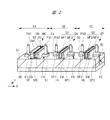
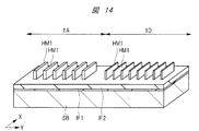
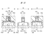
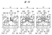
以下に、図2〜図5を用いて、本実施の形態の半導体装置の構造について説明する。図2は、本実施の形態における半導体装置の平面図である。図3は、本実施の形態における半導体装置の斜視図である。図4および図5は、本実施の形態における半導体装置の断面図である。なお、図3、図5では、ウェルの図示を省略する。また、図5では、ソース・ドレイン領域の図示を省略する。
<Device structure of semiconductor device>
The structure of the semiconductor device according to the present embodiment will be described below with reference to FIGS. FIG. 2 is a plan view of the semiconductor device according to the present embodiment. FIG. 3 is a perspective view of the semiconductor device according to the present embodiment. 4 and 5 are cross-sectional views of the semiconductor device according to the present embodiment. 3 and 5, illustration of the well is omitted. In FIG. 5, illustration of the source / drain regions is omitted.
図2において、メモリセル領域1Aにはメモリセルアレイの平面図を示し、nMIS領域1Bには、ロジック回路領域のロジック回路などを構成するn型トランジスタQNの平面図を示し、pMIS領域1Cには、ロジック回路領域のロジック回路などを構成するp型トランジスタQPの平面図を示している。n型トランジスタQNとしては、n型のMISFET(Metal Insulator Semiconductor Field Effect Transistor)を例示する。p型トランジスタQPとしては、p型のMISFETを例示する。本願では、n型のMISFETをnMISと呼び、p型のMISFETをpMISと呼ぶ場合がある。
In FIG. 2, a
メモリセル領域1Aに形成されるメモリセルMCは、例えば図1のフラッシュメモリCC5に形成されている。また、nMIS領域1Bのn型トランジスタQNおよびpMIS領域1Cのp型トランジスタQPは、例えばRAMCC2、CPUCC1などに形成されている。
The memory cells MC formed in the
図2に示すように、メモリセル領域1Aには、X方向に延在する複数のフィンFAが、Y方向に等間隔に配置されている。X方向およびY方向は、半導体基板SBの主面に沿う方向であり。X方向はY方向に対して直交している。フィンFAは、例えば、半導体基板SBの主面から選択的に突出した直方体の突出部(凸部)であり、壁状(板状)の形状を有している。フィンFAの下端部分は、半導体基板SBの主面を覆う素子分離膜EIで囲まれている。フィンFAは、半導体基板SBの一部であり、半導体基板SBの活性領域である。平面視において、隣り合うフィンFA同士の間は、素子分離膜EIで埋まっており、フィンFAの周囲は、素子分離膜EIで囲まれている。フィンFAは、メモリセルMCを形成するための活性領域である。
As shown in FIG. 2, a plurality of fins FA extending in the X direction are arranged at equal intervals in the Y direction in the
複数のフィンFA上には、Y方向に延在する複数の制御ゲート電極CGおよび複数のメモリゲート電極MGが配置されている。フィンFAの上面には、制御ゲート電極CGおよびメモリゲート電極MGを挟むように、制御ゲート電極CGの側のドレイン領域MDと、メモリゲート電極側のソース領域MSとが形成されている。すなわち、X方向において、互いに隣り合う1つの制御ゲート電極CGおよび1つのメモリゲート電極MGは、ソース領域MSとドレイン領域MDとの間に位置している。 A plurality of control gate electrodes CG and a plurality of memory gate electrodes MG extending in the Y direction are arranged on the plurality of fins FA. On the upper surface of the fin FA, a drain region MD on the control gate electrode CG side and a source region MS on the memory gate electrode side are formed so as to sandwich the control gate electrode CG and the memory gate electrode MG. That is, one control gate electrode CG and one memory gate electrode MG adjacent to each other in the X direction are located between the source region MS and the drain region MD.
ドレイン領域MDおよびソース領域MSは、n型の半導体領域である。ドレイン領域MDは、X方向において隣り合う2つの制御ゲート電極CG同士の間に形成されており、ソース領域MSは、X方向において隣り合う2つのメモリゲート電極MG同士の間に形成されている。メモリセルMCは、制御ゲート電極CG、メモリゲート電極MG、ドレイン領域MDおよびソース領域MSを有する不揮発性記憶素子である。以下では、1つのメモリセルMCを構成するソース領域MSおよびドレイン領域MDを、ソース・ドレイン領域と呼ぶ場合がある。 The drain region MD and the source region MS are n-type semiconductor regions. The drain region MD is formed between two control gate electrodes CG adjacent in the X direction, and the source region MS is formed between two memory gate electrodes MG adjacent in the X direction. The memory cell MC is a nonvolatile memory element having a control gate electrode CG, a memory gate electrode MG, a drain region MD, and a source region MS. Hereinafter, the source region MS and the drain region MD constituting one memory cell MC may be referred to as source / drain regions.
X方向に隣接する2つのメモリセルMCは、ドレイン領域MDまたはソース領域MSを共有している。ドレイン領域MDを共有する2つのメモリセルMCは、Y方向に延在するドレイン領域MDを軸として、X方向に線対称となっており、ソース領域MSを共有する2つのメモリセルMCは、Y方向に延在するソース領域MSを軸として、X方向に線対称となっている。 Two memory cells MC adjacent in the X direction share the drain region MD or the source region MS. The two memory cells MC sharing the drain region MD are line-symmetric in the X direction with the drain region MD extending in the Y direction as an axis, and the two memory cells MC sharing the source region MS It is line symmetric in the X direction with the source region MS extending in the direction as an axis.
各フィンFAには、X方向に並ぶ複数のメモリセルMCが形成されている。各メモリセルMCのドレイン領域MDは、メモリセルMC上に形成された層間絶縁膜(図示しない)を貫通するコンタクトホール内に形成されたプラグ(コンタクトプラグ)PG1を介して、X方向に延在する配線MWからなるソース線SLに電気的に接続されている。また、Y方向に配列された複数のメモリセルMCのソース領域MSは、Y方向に延在する配線MWからなるビット線BLに電気的に接続されている。 A plurality of memory cells MC arranged in the X direction are formed on each fin FA. The drain region MD of each memory cell MC extends in the X direction via a plug (contact plug) PG1 formed in a contact hole penetrating an interlayer insulating film (not shown) formed on the memory cell MC. Is electrically connected to a source line SL made of a wiring MW . Further, the source regions MS of the plurality of memory cells MC arranged in the Y direction are electrically connected to a bit line BL including a wiring MW extending in the Y direction.
また、nMIS領域1Bには、例えば、X方向に延在するフィンFBが形成されている。フィンFBは、フィンFAと同様に半導体基板SBの一部であり、半導体基板SBの主面上に突出した壁状(板状)の形状を有している。また、フィンFBは、半導体基板SBの活性領域であり、フィンFBの下端部分は、半導体基板SBの主面を覆う素子分離膜EIで囲まれている。フィンFB上には、Y方向に延在するゲート電極G1が配置され、ゲート電極G1を挟むように、フィンFBの上面にはドレイン領域LD1およびソース領域LS1が形成されている。ドレイン領域LD1およびソース領域LS1は、n型の半導体領域である。
In the
n型トランジスタQNは、ゲート電極G1、ドレイン領域LD1およびソース領域LS1を有する。ゲート電極G1、ドレイン領域LD1およびソース領域LS1は、それぞれ、コンタクトホール内に形成されたプラグPGを介して、配線MWに電気的に接続されている。フィンFBは、n型トランジスタQNを形成するための活性領域である。 The n-type transistor QN has a gate electrode G1, a drain region LD1, and a source region LS1. The gate electrode G1, the drain region LD1, and the source region LS1 are each electrically connected to a wiring MW via a plug PG formed in a contact hole. Fin FB is an active region for forming n-type transistor QN.
また、pMIS領域1Cには、X方向に延在するフィンFCと、その上部のp型トランジスタQPが形成されている。ゲート電極G2、ドレイン領域LD2およびソース領域LS2により構成されるp型トランジスタQPのレイアウトは、例えば、n型トランジスタQNと同様である。
In the
フィンFA、FBおよびFCは、半導体基板SBの主面から、主面に対して垂直な方向に突出する、例えば、直方体の突出部である。フィンFA、FBおよびFCは、必ずしも直方体である必要はなく、短辺方向における断面視にて、長方形の角部が丸みを帯びていてもよい。また、図5に示すように、フィンFA、FBおよびFCのそれぞれの側壁は半導体基板SBの主面に対して垂直であってもよいが、垂直に近い傾斜角度を有していてもよい。つまり、フィンFA、FBおよびFCのそれぞれの断面形状は、直方体であるか、または台形である。ここでは、フィンFA、FBおよびFCのそれぞれの側壁は、半導体基板SBの主面に対して斜めに傾斜している。 The fins FA, FB, and FC are, for example, rectangular projections that project from the main surface of the semiconductor substrate SB in a direction perpendicular to the main surface. The fins FA, FB, and FC do not necessarily have to be rectangular parallelepiped, and may have rounded corners of a rectangle in a cross-sectional view in the short side direction. Further, as shown in FIG. 5, the respective side walls of the fins FA, FB, and FC may be perpendicular to the main surface of the semiconductor substrate SB, or may have an inclination angle close to perpendicular. That is, the cross-sectional shape of each of the fins FA, FB, and FC is a rectangular parallelepiped or a trapezoid. Here, each side wall of the fins FA, FB and FC is obliquely inclined with respect to the main surface of the semiconductor substrate SB.
また、図2に示すように、平面視でフィンFA、FBおよびFCが延在する方向が各フィンの長辺方向であり、当該長辺方向に直交する方向が各フィンの短辺方向である。つまり、フィンの長さは、フィンの幅よりも大きい。フィンFA、FBおよびFCは、長さ、幅、および、高さを有する突出部であれば、その形状は問わない。例えば、平面視で、蛇行するレイアウトを有していてもよい。 As shown in FIG. 2, the direction in which the fins FA, FB, and FC extend in plan view is the long side direction of each fin, and the direction orthogonal to the long side direction is the short side direction of each fin. . That is, the length of the fin is larger than the width of the fin. The shapes of the fins FA, FB, and FC are not limited as long as they have a length, a width, and a height. For example, it may have a meandering layout in plan view.
図3〜図5では、左側から右側に向かって順にメモリセル領域1A、nMIS領域1BおよびpMIS領域1Cが並んで示されている。図3では、素子分離膜EIおよび各素子の上の層間絶縁膜および配線の図示を省略している。メモリセル領域1Aの半導体基板SBを構成するフィンFAの上部にはメモリセルMCが形成され、nMIS領域1Bの半導体基板SBを構成するフィンFBの上部にはn型トランジスタQNが形成され、pMIS領域1Cの半導体基板SBを構成するフィンFCの上部にはp型トランジスタQPが形成されている。
3 to 5, the
図4は、図2のA−A線、B−B線およびC−C線における半導体素子の断面を示すものである。図5は、図2のD−D線、E−E線およびF−F線における半導体素子の断面を示すものである。1つのフィン上には複数の素子が並んで形成されているが、図3、4では、フィン上に素子を1つのみ示している。 FIG. 4 is a cross-sectional view of the semiconductor device taken along line AA, line BB, and line CC in FIG. FIG. 5 is a cross-sectional view of the semiconductor device taken along line DD, line EE, and line FF in FIG. Although a plurality of elements are formed side by side on one fin, FIGS. 3 and 4 show only one element on the fin.
図3に示すように、制御ゲート電極CGおよびメモリゲート電極MGは、フィンFAを跨ぐようにY方向に延在し、ゲート電極G1はフィンFBを跨ぐようにY方向に延在し、ゲート電極G2はフィンFCを跨ぐようにY方向に延在している。制御ゲート電極CGおよびメモリゲート電極MGのそれぞれの上面は、シリサイド層S2により覆われている。シリサイド層S2は、例えばNiSi(ニッケルシリサイド)からなる。なお、シリサイド層S2はPt(白金)を含んでいてもよい。 As shown in FIG. 3, the control gate electrode CG and the memory gate electrode MG extend in the Y direction so as to straddle the fin FA. The gate electrode G1 extends in the Y direction so as to straddle the fin FB. G2 extends in the Y direction so as to straddle the fin FC. The respective upper surfaces of the control gate electrode CG and the memory gate electrode MG are covered with a silicide layer S2. The silicide layer S2 is made of, for example, NiSi (nickel silicide). Note that the silicide layer S2 may include Pt (platinum).
図3〜図5に示すように、メモリセル領域1Aのソース・ドレイン領域を構成する拡散領域D1が形成されたフィンFAの側壁および上面は、シリサイド層S1により覆われている。シリサイド層S1は、例えばNiSi(ニッケルシリサイド)からなる。また、nMIS領域1Bのソース・ドレイン領域を構成する拡散領域D2が形成されたフィンFBの側壁および上面は、エピタキシャル層(半導体層)EP1により覆われている。同様に、pMIS領域1Cのソース・ドレイン領域を構成する拡散領域D3が形成されたフィンFCの側壁および上面は、エピタキシャル層(半導体層)EP2により覆われている。
As shown in FIGS. 3 to 5, the side wall and the upper surface of the fin FA where the diffusion region D1 constituting the source / drain region of the
シリサイド層S1、エピタキシャル層EP1およびEP2は、いずれも素子分離膜EI上に形成されている。シリサイド層S1は、フィンFAの上面および側壁に沿って延在する層からなる。 The silicide layer S1 and the epitaxial layers EP1 and EP2 are all formed on the element isolation film EI. The silicide layer S1 is a layer extending along the upper surface and the side wall of the fin FA.
これに対し、エピタキシャル成長法により形成されたエピタキシャル層EP1、EP2は、Y方向に沿う断面(図5参照)において、菱形の形状を有している。すなわち、nMIS領域1Bのエピタキシャル層EP1の側壁であって、フィンFBに接していない側壁は、下部の側壁および上部の側壁を有している。当該下部の側壁は素子分離膜EI側から上方に向かうにつれて、半導体基板SBの主面に沿う方向においてフィンFBから離れるような傾斜を有しており、当該上部の側壁は素子分離膜EI側から上方に向かうにつれて、半導体基板SBの主面に沿う方向においてフィンFBに近付くような傾斜を有している。当該下部の側壁の上端と、当該上部の側壁の下端は接続されている。
On the other hand, the epitaxial layers EP1 and EP2 formed by the epitaxial growth method have a rhombic shape in a cross section along the Y direction (see FIG. 5). That is, the side wall of the epitaxial layer EP1 in the
言い換えれば、Y方向において、エピタキシャル層EP1の左側の終端部と右側の終端部との間の幅は、エピタキシャル層EP1の上端および下端に比べて、当該上端および当該下端の間の中心部の方が大きい。なお、pMIS領域1Cのエピタキシャル層EP2も、nMIS領域1Bのエピタキシャル層EP1と同様の形状を有している。nMIS領域1Bのエピタキシャル層EP1は、例えばSiP(リン化シリコン)またはSiC(炭化シリコン)からなり、pMIS領域1Cのエピタキシャル層EP2は、SiGe(シリコンゲルマニウム)からなる。
In other words, in the Y direction, the width between the left end and the right end of the epitaxial layer EP1 is closer to the center between the upper end and the lower end than to the upper end and the lower end of the epitaxial layer EP1. Is big. The epitaxial layer EP2 in the
nMIS領域1Bのエピタキシャル層EP1は、n型の不純物(例えばP(リン)またはAs(ヒ素))が導入された半導体層であり、n型トランジスタQNの拡散領域D2を構成している。pMIS領域1Cのエピタキシャル層EP2は、p型の不純物(例えばB(ホウ素))が導入された半導体層であり、p型トランジスタQPの拡散領域D3を構成している。
The epitaxial layer EP1 of the
図3および図4に示すように、フィンFA、FBおよびFCのそれぞれの側壁の下部は、半導体基板SBの主面上に形成された素子分離膜EIで囲まれている。つまり、各フィン同士の間は、素子分離膜EIで分離されている。フィンFA内には、フィンFAの上面から下部に亘ってp型の半導体領域であるp型ウェルPW1が形成されている。同様に、フィンFB内には、フィンFBの上面から下部に亘ってp型の半導体領域であるp型ウェルPW2が形成されている。また、フィンFCには、フィンFCの上面から下部に亘ってn型の半導体領域であるn型ウェルNWが形成されている。 As shown in FIGS. 3 and 4, the lower portions of the side walls of the fins FA, FB, and FC are surrounded by an element isolation film EI formed on the main surface of the semiconductor substrate SB. That is, the fins are separated by the element isolation film EI. In the fin FA, a p-type well PW1, which is a p-type semiconductor region, is formed from the upper surface to the lower portion of the fin FA. Similarly, in the fin FB, a p-type well PW2 which is a p-type semiconductor region is formed from the upper surface to the lower portion of the fin FB. In the fin FC, an n-type well NW, which is an n-type semiconductor region, is formed from the upper surface to the lower portion of the fin FC.
フィンFAの上面上および側面上には、ゲート絶縁膜GFを介して制御ゲート電極CGが形成されており、フィンFAの長辺方向(X方向)において、制御ゲート電極CGに隣り合う領域には、絶縁膜ONを介してメモリゲート電極MGが形成されている。制御ゲート電極CGとメモリゲート電極MGとの間には、絶縁膜ONが介在しており、制御ゲート電極CGとメモリゲート電極MGとの間は、絶縁膜ONで電気的に分離されている。また、メモリゲート電極MGとフィンFAの上面との間には、絶縁膜ONが介在している。絶縁膜ONはメモリゲート電極MGの側壁および底面を覆うように連続的に形成されている。このため、絶縁膜ONはL字型の断面形状を有する。 A control gate electrode CG is formed on the upper surface and the side surface of the fin FA with a gate insulating film GF interposed therebetween. In a long side direction (X direction) of the fin FA, a region adjacent to the control gate electrode CG is formed. The memory gate electrode MG is formed via the insulating film ON. An insulating film ON is interposed between the control gate electrode CG and the memory gate electrode MG, and the control gate electrode CG and the memory gate electrode MG are electrically separated by the insulating film ON. Further, an insulating film ON is interposed between the memory gate electrode MG and the upper surface of the fin FA. The insulating film ON is formed continuously so as to cover the side wall and the bottom surface of the memory gate electrode MG. For this reason, the insulating film ON has an L-shaped cross section.
ゲート絶縁膜GFは、シリコンからなる半導体基板SBの突出部であるフィンFAの主面および側面を熱酸化して形成した熱酸化膜(酸化シリコン膜)であり、その膜厚は例えば2nmである。また、絶縁膜ONは、シリコンからなる半導体基板SBの突出部であるフィンFAの主面および側面を熱酸化して形成した4nmの膜厚を有する熱酸化膜(酸化シリコン膜)からなる酸化シリコン膜X1と、酸化シリコン膜X1上に形成された窒化シリコン膜NFと、窒化シリコン膜NF上に形成された酸化シリコン膜X2とからなる。窒化シリコン膜NFは、メモリセルMCの電荷蓄積部(電荷蓄積層)である。窒化シリコン膜は、例えば7nmの膜厚を有し、酸化シリコン膜X2は、例えば9nmの膜厚を有する。 The gate insulating film GF is a thermal oxide film (silicon oxide film) formed by thermally oxidizing the main surface and side surfaces of the fin FA, which is a protrusion of the semiconductor substrate SB made of silicon, and has a thickness of, for example, 2 nm. . The insulating film ON is formed of a thermal oxide film (silicon oxide film) having a thickness of 4 nm formed by thermally oxidizing the main surface and side surfaces of the fin FA, which is a protruding portion of the semiconductor substrate SB made of silicon. It comprises a film X1, a silicon nitride film NF formed on the silicon oxide film X1, and a silicon oxide film X2 formed on the silicon nitride film NF. The silicon nitride film NF is a charge storage portion (charge storage layer) of the memory cell MC. The silicon nitride film has a thickness of, for example, 7 nm, and the silicon oxide film X2 has a thickness of, for example, 9 nm.
つまり、絶縁膜ONは、フィンFAの上面側および制御ゲート電極CGの側壁側から順に積層された酸化シリコン膜X1、窒化シリコン膜NFおよび酸化シリコン膜X2からなる積層構造を有する。絶縁膜ONの膜厚は、例えば20nmであり、制御ゲート電極CG下のゲート絶縁膜GFの膜厚よりも大きい。酸化シリコン膜X2は、酸窒化シリコン膜により形成してもよい。 That is, the insulating film ON has a stacked structure including the silicon oxide film X1, the silicon nitride film NF, and the silicon oxide film X2 sequentially stacked from the upper surface side of the fin FA and the side wall side of the control gate electrode CG. The thickness of the insulating film ON is, for example, 20 nm, which is larger than the thickness of the gate insulating film GF below the control gate electrode CG. The silicon oxide film X2 may be formed using a silicon oxynitride film.
メモリセル領域1Aに示すように、フィンFAの短辺方向(Y方向)において、制御ゲート電極CGは、ゲート絶縁膜GFを介して、フィンFAの上面、側面および素子分離膜EIの上面に沿って延在している。同様に、フィンFAの短辺方向において、メモリゲート電極MGは、絶縁膜ONを介して、フィンFAの主面、側面および素子分離膜EIの上面に沿って延在している。制御ゲート電極CGおよびメモリゲート電極MGのそれぞれの主面上にはシリサイド層S2が形成されている。
As shown in the
また、制御ゲート電極CG、メモリゲート電極MG、ゲート絶縁膜GF、絶縁膜ONおよびシリサイド層S2を含むパターンの側壁は、サイドウォール(サイドウォールスペーサ)SWにより覆われている。サイドウォールSWは、例えば窒化シリコン膜および酸化シリコン膜の積層構造からなる。シリサイド層S1は、制御ゲート電極CGを含む当該パターンおよび上記サイドウォールSWから露出するフィンFAの表面を覆っている。 The side wall of the pattern including the control gate electrode CG, the memory gate electrode MG, the gate insulating film GF, the insulating film ON, and the silicide layer S2 is covered with a side wall (side wall spacer) SW. The sidewall SW has a stacked structure of, for example, a silicon nitride film and a silicon oxide film. The silicide layer S1 covers the pattern including the control gate electrode CG and the surface of the fin FA exposed from the sidewall SW.
図4に示すように、制御ゲート電極CGを含む当該パターンの直下のフィンFAの上面を挟むように、一対のソース・ドレイン領域がフィンFAの上面に形成されている。ソース領域およびドレイン領域のそれぞれは、n−型半導体領域であるエクステンション領域EX1およびn+型半導体領域である拡散領域D1を有する。拡散領域D1は、エクステンション領域EX1に比べて不純物濃度が高く、形成深さが深い。ソース領域およびドレイン領域のそれぞれにおいてエクステンション領域EX1および拡散領域D1は互いに接しており、エクステンション領域EX1は、拡散領域D1よりも上記パターンの直下のフィンFAの上面、つまりチャネル領域側に位置している。 As shown in FIG. 4, a pair of source / drain regions are formed on the upper surface of the fin FA so as to sandwich the upper surface of the fin FA immediately below the pattern including the control gate electrode CG. Each of the source region and the drain region has an extension region EX1 which is an n − type semiconductor region and a diffusion region D1 which is an n + type semiconductor region. The diffusion region D1 has a higher impurity concentration and a deeper formation depth than the extension region EX1. In each of the source region and the drain region, the extension region EX1 and the diffusion region D1 are in contact with each other, and the extension region EX1 is located on the upper surface of the fin FA immediately below the pattern, that is, on the channel region side from the diffusion region D1. .
このように、不純物濃度が低いエクステンション領域EX1と、不純物濃度が高い拡散領域D1とを備えた構造、つまりLDD(Lightly Doped Drain)構造を有するソース・ドレイン領域を形成することで、当該ソース・ドレイン領域を有するトランジスタの短チャネル特性を改善することができる。当該ソース領域は、図2に示すソース領域MSに相当し、当該ドレイン領域は、図2に示すドレイン領域MDに相当する。 As described above, by forming a source / drain region having a structure including the extension region EX1 having a low impurity concentration and the diffusion region D1 having a high impurity concentration, that is, an LDD (Lightly Doped Drain) structure, the source / drain is formed. The short-channel characteristics of the transistor including the region can be improved. The source region corresponds to the source region MS illustrated in FIG. 2, and the drain region corresponds to the drain region MD illustrated in FIG.
フィンFA上および素子分離膜EI上には、例えば酸化シリコン膜からなる層間絶縁膜IL1が形成されている。また、層間絶縁膜IL1、制御ゲート電極CG、メモリゲート電極MG、サイドウォールSWおよびシリサイド層S2のそれぞれの上面上には、例えば酸化シリコン膜からなる層間絶縁膜IL2が形成されている。層間絶縁膜IL1の上面は、絶縁膜ON、サイドウォールSWおよびシリサイド層S2のそれぞれの上面と略同一の面において平坦化されている。 On the fin FA and the element isolation film EI, an interlayer insulating film IL1 made of, for example, a silicon oxide film is formed. Further, an interlayer insulating film IL2 made of, for example, a silicon oxide film is formed on each of the upper surfaces of the interlayer insulating film IL1, the control gate electrode CG, the memory gate electrode MG, the sidewall SW, and the silicide layer S2. The upper surface of the interlayer insulating film IL1 is flattened on substantially the same surface as the respective upper surfaces of the insulating film ON, the sidewall SW, and the silicide layer S2.
層間絶縁膜IL2上には複数の配線M1が形成され、配線M1は、層間絶縁膜IL2およびIL1を貫通するコンタクトホールCH内に設けられたプラグPG1を介して、メモリセルMCの上記ソース領域および上記ドレイン領域に電気的に接続されている。すなわち、プラグPG1の底面は、シリサイド層S1の上面に直接接しており、プラグPG1はシリサイド層S1を介してソース・ドレイン領域に電気的に接続されている。シリサイド層S1は、例えばタングステン(W)を主に含む金属膜からなる接続部であるプラグPG1と、半導体からなるフィンFA内のソース・ドレイン領域との間の接続抵抗を低減する役割を有する。 A plurality of wirings M1 are formed on the interlayer insulating film IL2, and the wiring M1 is connected to the source region and the memory cell MC via a plug PG1 provided in a contact hole CH passing through the interlayer insulating film IL2 and IL1. It is electrically connected to the drain region. That is, the bottom surface of the plug PG1 is in direct contact with the upper surface of the silicide layer S1, and the plug PG1 is electrically connected to the source / drain region via the silicide layer S1. The silicide layer S1 has a role of reducing the connection resistance between the plug PG1, which is a connection portion made of a metal film mainly containing, for example, tungsten (W), and the source / drain region in the fin FA made of a semiconductor.
ここでは、コンタクトホールCH、プラグPG1およびPG2のそれぞれが平面視において丸い形状を有する場合について説明するが、コンタクトホールCH、プラグPG1およびPG2の平面視における形状は矩形であってもよい。また、コンタクトホールCH、プラグPG1およびPG2が、各フィンの短辺方向(Y方向)において、シリサイド層S1、エピタキシャル層EP1およびEP2よりも大きい幅を有していてもよい。 Here, the case where each of contact hole CH and plugs PG1 and PG2 has a round shape in plan view will be described, but the shape of contact hole CH and plugs PG1 and PG2 in plan view may be rectangular. Further, contact hole CH and plugs PG1 and PG2 may have a width greater than silicide layer S1 and epitaxial layers EP1 and EP2 in the short side direction (Y direction) of each fin.
また、ソース・ドレイン領域が形成されたフィンFAをシリサイド層S1により覆うことで、ソース・ドレイン領域を低抵抗化し、これによりメモリセルMCの性能を向上させることができる。 In addition, by covering the fin FA on which the source / drain region is formed with the silicide layer S1, the resistance of the source / drain region can be reduced, thereby improving the performance of the memory cell MC.
メモリセルMCは、制御ゲート電極CG、メモリゲート電極MG、ドレイン領域およびソース領域を有する。制御ゲート電極CGおよびソース・ドレイン領域は制御トランジスタを構成し、メモリゲート電極MGおよびソース・ドレイン領域はメモリトランジスタを構成し、メモリセルMCは制御トランジスタおよびメモリトランジスタにより構成されている。つまり、制御トランジスタとメモリトランジスタとは、ソース・ドレイン領域を共有している。また、制御ゲート電極CGおよびメモリゲート電極MGのゲート長方向(X方向)のドレイン領域とソース領域との間の距離が、メモリセルMCのチャネル長に相当する。 The memory cell MC has a control gate electrode CG, a memory gate electrode MG, a drain region, and a source region. The control gate electrode CG and the source / drain region constitute a control transistor, the memory gate electrode MG and the source / drain region constitute a memory transistor, and the memory cell MC comprises a control transistor and a memory transistor. That is, the control transistor and the memory transistor share the source / drain region. The distance between the drain region and the source region in the gate length direction (X direction) of the control gate electrode CG and the memory gate electrode MG corresponds to the channel length of the memory cell MC.
nMIS領域1Bにおいて、フィンFBの主面および側面上には、ゲート絶縁膜として機能する絶縁膜HKを介してゲート電極G1が形成されている。なお、絶縁膜HKはゲート電極G1の底面と側壁とを連続的に覆っている。絶縁膜HKは、窒化シリコンよりも誘電率(比誘電率)が高い絶縁材料膜、いわゆるHigh−k膜(高誘電率膜)である。また、ゲート電極G1は、絶縁膜HKの表面を覆う金属膜MF1と、絶縁膜HK上に金属膜MF1上を介して形成された金属膜MF2とからなる。金属膜MF1は例えばTiAl(チタンアルミニウム)からなり、金属膜MF2は例えばAl(アルミニウム)からなる。なお、フィンFBと絶縁膜HKとの間に酸化シリコン膜がゲート絶縁膜の一部として形成されていてもよいが、ここでは図示しない。
In the
フィンFBの短辺方向(Y方向)において、ゲート電極G1は、絶縁膜HKを介して、フィンFBの上面、側面および素子分離膜EIの上面のそれぞれに沿って連続的に延在している。また、ゲート電極G1の側壁は、サイドウォールSWにより覆われている。 In the short side direction (Y direction) of the fin FB, the gate electrode G1 continuously extends along the upper surface and the side surface of the fin FB and the upper surface of the element isolation film EI via the insulating film HK. . Further, the side wall of the gate electrode G1 is covered with the side wall SW.
また、X方向においてゲート電極G1を挟むように、ゲート電極G1の横の領域に設けられたソース領域およびドレイン領域のそれぞれは、n−型半導体領域であるエクステンション領域EX2と、n+型半導体領域である拡散領域D2とを有し、LDD構造を有している。拡散領域D2は、フィンFB内と、ゲート電極G1の横にサイドウォールSWを介して形成されたエピタキシャル層EP1内とに亘って形成されている。エクステンション領域EX2は、フィンFB内に形成されている。当該ソース領域は、図2に示すソース領域LS1に相当し、当該ドレイン領域は、図2に示すドレイン領域LD1に相当する。 Each of a source region and a drain region provided in a region next to the gate electrode G1 so as to sandwich the gate electrode G1 in the X direction includes an extension region EX2 that is an n − type semiconductor region and an n + type semiconductor region. , And an LDD structure. The diffusion region D2 is formed over the inside of the fin FB and the inside of the epitaxial layer EP1 formed on the side of the gate electrode G1 via the sidewall SW. The extension region EX2 is formed in the fin FB. The source region corresponds to the source region LS1 shown in FIG. 2, and the drain region corresponds to the drain region LD1 shown in FIG.
また、nMIS領域1Bにおいて、フィンFB上および素子分離膜EI上には、メモリセル領域1Aと同様に層間絶縁膜IL1、IL2が順に形成されている。ただし、層間絶縁膜IL1と層間絶縁膜IL2との間には、ゲート電極G1の上面を覆うように絶縁膜IF9が形成されている。層間絶縁膜IL1の上面は、ゲート電極G1、絶縁膜HKおよびサイドウォールSWのそれぞれの上面と共に平坦化されている。層間絶縁膜IL1は、エピタキシャル層EP1の上面を覆っており、エピタキシャル層EP1の上面と層間絶縁膜IL1とは直接接している。つまり、エピタキシャル層EP1の上面と層間絶縁膜IL1との間にはシリサイド層は介在していない。
In the
層間絶縁膜IL2上には、配線M1が形成され、配線M1は、層間絶縁膜IL2およびIL1を貫通するコンタクトホールCH内に設けられたプラグPG2を介して、ソース領域およびドレイン領域に電気的に接続されている。プラグPG2とエピタキシャル層EP1との間には、シリサイド層S3が介在している。シリサイド層S3は、例えばTiSi2(チタンシリサイド)からなる。 Over the interlayer insulating film IL2, a wiring M1 is formed. The wiring M1 is electrically connected to the source region and the drain region via a plug PG2 provided in a contact hole CH penetrating the interlayer insulating film IL2 and IL1. It is connected. A silicide layer S3 is interposed between the plug PG2 and the epitaxial layer EP1. The silicide layer S3 is made of, for example, TiSi 2 (titanium silicide).
シリサイド層S3は、プラグPG2の直下、つまり、コンタクトホールCHの底部にのみ形成されており、プラグPG2の横の領域のエピタキシャル層EP1の上面は、シリサイド層S3から露出している。シリサイド層S3は、例えばタングステン(W)を主に含む金属膜からなる接続部であるプラグPG2と、半導体からなるエピタキシャル層EP1内のソース・ドレイン領域との間の接続抵抗を低減する役割を有する。 The silicide layer S3 is formed immediately below the plug PG2, that is, only at the bottom of the contact hole CH, and the upper surface of the epitaxial layer EP1 in a region next to the plug PG2 is exposed from the silicide layer S3. The silicide layer S3 has a role of reducing the connection resistance between the plug PG2, which is a connection part made of a metal film mainly containing, for example, tungsten (W), and the source / drain region in the semiconductor epitaxial layer EP1. .
n型トランジスタQNは、ゲート電極G1、ドレイン領域および、ソース領域を有する。そして、ゲート電極G1のゲート長方向(X方向)のドレイン領域とソース領域との間の距離が、n型トランジスタQNのチャネル長に相当する。 N-type transistor QN has a gate electrode G1, a drain region, and a source region. The distance between the drain region and the source region of the gate electrode G1 in the gate length direction (X direction) corresponds to the channel length of the n-type transistor QN.
pMIS領域1Cにおいて、フィンFCの主面および側面上には、ゲート絶縁膜として機能する絶縁膜HKを介してゲート電極G2が形成されている。なお、絶縁膜HKはゲート電極G2の底面と側壁とを連続的に覆っている。絶縁膜HKは、窒化シリコンよりも誘電率(比誘電率)が高い絶縁材料膜、いわゆるHigh−k膜(高誘電率膜)である。また、ゲート電極G2は、絶縁膜HKの表面を覆う金属膜MF3と、絶縁膜HK上に金属膜MF3上を介して形成された金属膜MF4とからなる。金属膜MF3は例えばTiAl(チタンアルミニウム)からなり、金属膜MF4は例えばAl(アルミニウム)からなる。なお、フィンFCと絶縁膜HKとの間に酸化シリコン膜がゲート絶縁膜の一部として形成されていてもよいが、ここでは図示しない。
In the
フィンFCの短辺方向(Y方向)において、ゲート電極G2は、絶縁膜HKを介して、フィンFCの上面、側面および素子分離膜EIの上面のそれぞれに沿って連続的に延在している。また、ゲート電極G2の側壁は、サイドウォールSWにより覆われている。 In the short side direction (Y direction) of the fin FC, the gate electrode G2 continuously extends along the upper surface and the side surface of the fin FC and the upper surface of the element isolation film EI via the insulating film HK. . Further, the side wall of the gate electrode G2 is covered with the side wall SW.
また、X方向においてゲート電極G2を挟むように、ゲート電極G2の横の領域に設けられたソース領域およびドレイン領域のそれぞれは、p−型半導体領域であるエクステンション領域EX3と、p+型半導体領域である拡散領域D3とを有し、LDD構造を有している。拡散領域D3は、フィンFC内と、ゲート電極G2の横にサイドウォールSWを介して形成されたエピタキシャル層EP2内とに亘って形成されている。エクステンション領域EX3は、フィンFC内に形成されている。当該ソース領域は、図2に示すソース領域LS2に相当し、当該ドレイン領域は、図2に示すドレイン領域LD2に相当する。 Each of a source region and a drain region provided in a region beside the gate electrode G2 so as to sandwich the gate electrode G2 in the X direction includes an extension region EX3, which is a p − type semiconductor region, and a p + type semiconductor region. And an LDD structure. The diffusion region D3 is formed over the inside of the fin FC and the inside of the epitaxial layer EP2 formed via the sidewall SW beside the gate electrode G2. The extension region EX3 is formed in the fin FC. The source region corresponds to the source region LS2 illustrated in FIG. 2, and the drain region corresponds to the drain region LD2 illustrated in FIG.
また、pMIS領域1Cにおいて、フィンFC上および素子分離膜EI上には、nMIS領域1Bと同様に層間絶縁膜IL1、絶縁膜IF9およびIL2が順に形成されている。層間絶縁膜IL1の上面は、ゲート電極G2、絶縁膜HKおよびサイドウォールSWのそれぞれの上面と共に平坦化されている。層間絶縁膜IL1は、エピタキシャル層EP2の上面を覆っており、エピタキシャル層EP2の上面と層間絶縁膜IL1とは直接接している。つまり、エピタキシャル層EP2の上面と層間絶縁膜IL1との間にはシリサイド層は介在していない。
Further, in the
層間絶縁膜IL2上には、配線M1が形成され、配線M1は、層間絶縁膜IL2およびIL1を貫通するコンタクトホールCH内に設けられたプラグPG2を介して、ソース領域およびドレイン領域に電気的に接続されている。プラグPG2とエピタキシャル層EP2との間には、シリサイド層S3が介在している。シリサイド層S3は、例えばTiSi2(チタンシリサイド)からなる。 Over the interlayer insulating film IL2, a wiring M1 is formed. The wiring M1 is electrically connected to the source region and the drain region via a plug PG2 provided in a contact hole CH penetrating the interlayer insulating film IL2 and IL1. It is connected. A silicide layer S3 is interposed between the plug PG2 and the epitaxial layer EP2. The silicide layer S3 is made of, for example, TiSi 2 (titanium silicide).
シリサイド層S3は、プラグPG2の直下、つまり、コンタクトホールCHの底部にのみ形成されており、プラグPG2の横の領域のエピタキシャル層EP2の上面は、シリサイド層S3から露出している。シリサイド層S3は、例えばタングステン(W)を主に含む金属膜からなる接続部であるプラグPG2と、半導体からなるエピタキシャル層EP2内のソース・ドレイン領域との間の接続抵抗を低減する役割を有する。 The silicide layer S3 is formed immediately below the plug PG2, that is, only at the bottom of the contact hole CH, and the upper surface of the epitaxial layer EP2 in a region next to the plug PG2 is exposed from the silicide layer S3. The silicide layer S3 has a role of reducing the connection resistance between the plug PG2, which is a connection part made of a metal film mainly containing, for example, tungsten (W), and the source / drain region in the epitaxial layer EP2 made of a semiconductor. .
p型トランジスタQPは、ゲート電極G2、ドレイン領域および、ソース領域を有する。そして、ゲート電極G2のゲート長方向(X方向)のドレイン領域とソース領域との間の距離が、p型トランジスタQPのチャネル長に相当する。 The p-type transistor QP has a gate electrode G2, a drain region, and a source region. The distance between the drain region and the source region in the gate length direction (X direction) of the gate electrode G2 corresponds to the channel length of the p-type transistor QP.
<半導体装置の効果について>
nMIS領域1BおよびpMIS領域1Cに形成されたエピタキシャル層EP1、EP2のそれぞれの上面であって、シリサイド層S3を介してプラグPG2に接続された面の位置は、シリサイド層S1の上面であって、プラグPG1に接続された面の位置よりも高い。これは、フィンFA上に形成されたシリサイド層S1の膜厚よりも、フィンFB上またはフィンFC上に形成されたエピタキシャル層EP1、EP2のそれぞれの膜厚の方が大きいためである。
<Effects of semiconductor device>
The upper surface of each of the epitaxial layers EP1 and EP2 formed in the
このように、厚いエピタキシャル層EP1、EP2を形成することで、本実施の形態では、ロジック領域のn型トランジスタQNおよびp型トランジスタQPのそれぞれのソース・ドレイン領域のそれぞれの断面積を増大させ、これにより当該ソース・ドレイン領域の抵抗を低減している。また、メモリセル領域1Aでは、半導体よりも低抵抗なシリサイド層S1によりフィンFAを覆うことで、ソース・ドレイン領域の抵抗を低減している。
By forming the thick epitaxial layers EP1 and EP2 as described above, in the present embodiment, the respective cross-sectional areas of the source / drain regions of the n-type transistor QN and the p-type transistor QP in the logic region are increased, Thereby, the resistance of the source / drain region is reduced. In the
このようにメモリセル領域1Aと、ロジック領域であるnMIS領域1BおよびpMIS領域1Cとで、ソース・ドレイン領域を低抵抗化するための構造が異なるのは、後述するように、応力の発生を防ぐ必要があるためである。すなわち、FINFETのソース・ドレイン領域を低抵抗化するためには、ソース・ドレイン領域を覆うエピタキシャル層を形成することが考えられるが、MONOS型のメモリセルにおいてエピタキシャル層を形成すると素子内に応力が発生し、これにより記憶装置としての性能および信頼性が低下する問題がある。
As described above, the structure for lowering the resistance of the source / drain region differs between the
そこで、本実施の形態では、MONOSメモリ型のメモリセルMCが形成されたフィンFAに対してはシリサイド層S1を形成することでソース・ドレイン領域の低抵抗化を実現し、ロジック領域のトランジスタ形成されたフィンFB、FCに対しては、体積の大きいエピタキシャル層EP1、EP2を形成することで、ソース・ドレイン領域の低抵抗化を実現している。 Therefore, in the present embodiment, the resistance of the source / drain region is reduced by forming the silicide layer S1 for the fin FA in which the MONOS memory type memory cell MC is formed, and the transistor in the logic region is formed. With respect to the fins FB and FC, the epitaxial layers EP1 and EP2 having a large volume are formed, thereby realizing low resistance of the source / drain regions.
以上より、メモリセルMC、n型トランジスタQNおよびp型トランジスタQPのそれぞれの低抵抗化を実現し、かつ、メモリセルの性能が低下することを防ぐことができる。したがって、半導体装置の性能を向上させることができる。 As described above, the resistance of each of the memory cell MC, the n-type transistor QN, and the p-type transistor QP can be reduced, and the performance of the memory cell can be prevented from deteriorating. Therefore, the performance of the semiconductor device can be improved.
なお、ロジック領域では、シリサイド層によりフィンFB、FC、エピタキシャル層EP1およびEP2を覆うことによる応力の増大を防ぐため、コンタクトホールCHの底部にのみシリサイド層S3を形成している。この場合、CVD法により形成することが可能な材料であるTi(チタン)膜を用いてサリサイドプロセスを行うことでシリサイド層S3を形成するため、シリサイド層S1とシリサイド層S3とは互いに異なる材料で形成される。また、シリサイド層S1の上面と、プラグPG1との間には、コンタクトホールCH内においてTi(チタン)膜が形成されていてもよい。 In the logic region, the silicide layer S3 is formed only at the bottom of the contact hole CH in order to prevent an increase in stress caused by covering the fins FB and FC and the epitaxial layers EP1 and EP2 with the silicide layer. In this case, since the silicide layer S3 is formed by performing a salicide process using a Ti (titanium) film that can be formed by a CVD method, the silicide layer S1 and the silicide layer S3 are made of different materials. It is formed. Further, a Ti (titanium) film may be formed in the contact hole CH between the upper surface of the silicide layer S1 and the plug PG1.
<半導体装置の製造工程について>
以下に、図6〜図53を用いて、本実施の形態の半導体装置の製造方法について説明する。図6、図8、図10、図12、図15、図17、図19、図20〜図40および図42〜図53は、本実施の形態の半導体装置の形成工程中の断面図である。図7、図9、図11、図13、図14、図16および図18は、本実施の形態の半導体装置の形成工程中の斜視図である。図41は、本実施の形態の半導体装置の形成工程に用いるスパッタリング装置の模式的な平面図である。図8、図10、図12、図15、図17および図19は、図7、図9、図11、図14、図16および図18の同じ位置におけるY方向に沿う断面を示す図である。上記斜視図、図42および図44では、ウェルの図示を省略する。
<About the manufacturing process of the semiconductor device>
The method of manufacturing the semiconductor device according to the present embodiment will be described below with reference to FIGS. 6, 8, 10, 12, 15, 17, 19, 20 to 40, and 42 to 53 are cross-sectional views of the semiconductor device of the present embodiment during the manufacturing process. . 7, 9, 11, 13, 14, 16, and 18 are perspective views of the semiconductor device according to the present embodiment during the formation process. FIG. 41 is a schematic plan view of a sputtering apparatus used in the formation process of the semiconductor device of the present embodiment. FIGS. 8, 10, 12, 15, 17, and 19 are cross-sectional views along the Y direction at the same positions in FIGS. 7, 9, 11, 14, 16, and 18. FIG. . In the perspective views, FIGS. 42 and 44, the illustration of the well is omitted.
図6〜図20では、左側から右側に向かって順に並ぶメモリセル領域1Aおよびロジック領域1Dを示している。また、図21〜図40、図42〜図53では、左側から右側に向かって順に並ぶメモリセル領域1A、nMIS領域1BおよびpMIS領域1Cを示している。nMIS領域1BおよびpMIS領域1Cは、ロジック領域1Dを構成する領域である。
6 to 20 show the
ここではまず、図6に示すように、半導体基板SBを用意し、半導体基板SBの主面上に、絶縁膜IF1、絶縁膜IF2および半導体膜SI1を順に形成する。半導体基板SBは、例えば1〜10Ωcm程度の比抵抗を有するp型の単結晶シリコンなどからなる。絶縁膜IF1は、例えば酸化シリコン膜からなり、例えば酸化法またはCVD(Chemical Vapor Deposition)法を用いて形成することができる。絶縁膜IF1の膜厚は、2〜10nm程度である。絶縁膜IF2は、例えば窒化シリコン膜からなり、その膜厚は、20〜100nm程度である。絶縁膜IF2は、例えばCVD法により形成する。半導体膜SI1は、例えばシリコン膜からなり、例えばCVD法により形成する。半導体膜SI1の膜厚は、例えば20〜200nmである。 Here, first, as shown in FIG. 6, a semiconductor substrate SB is prepared, and an insulating film IF1, an insulating film IF2, and a semiconductor film SI1 are sequentially formed on the main surface of the semiconductor substrate SB. The semiconductor substrate SB is made of, for example, p-type single-crystal silicon having a specific resistance of about 1 to 10 Ωcm. The insulating film IF1 is made of, for example, a silicon oxide film, and can be formed by using, for example, an oxidation method or a CVD (Chemical Vapor Deposition) method. The thickness of the insulating film IF1 is about 2 to 10 nm. The insulating film IF2 is made of, for example, a silicon nitride film and has a thickness of about 20 to 100 nm. The insulating film IF2 is formed by, for example, a CVD method. The semiconductor film SI1 is made of, for example, a silicon film, and is formed by, for example, a CVD method. The thickness of the semiconductor film SI1 is, for example, 20 to 200 nm.
次に、図7および図8に示すように、フォトリソグラフィ技術およびエッチング法を用いて、メモリセル領域1Aおよびロジック領域1Dの半導体膜SI1を加工する。これにより、絶縁膜IF2上には、X方向に延在する複数の半導体膜SI1のパターンが、Y方向に並んで複数形成される。図8は、図7に示す複数の半導体膜SI1のパターンを含む断面図である。
Next, as shown in FIGS. 7 and 8, the semiconductor film SI1 in the
メモリセル領域1Aの当該パターンのY方向の幅は、ロジック領域1Dの当該パターンのY方向の幅よりも大きい。また、Y方向において、メモリセル領域1Aに並ぶ当該パターン同士の間隔は、ロジック領域1Dに並ぶ当該パターン同士の間隔よりも大きい。後の工程では、Y方向において半導体膜SI1に近接する領域にフィンが形成されるため、当該パターンの幅および間隔を変更することにより、隣り合うフィン同士の間隔を調整することができる。
The width of the
次に、図9および図10に示すように、複数の半導体膜SI1のそれぞれの側壁を覆うハードマスクHM1を形成する。ここでは、例えば、半導体基板SB上にCVD法を用いて、10〜40nmの膜厚を有する酸化シリコン膜を形成した後、異方性エッチングであるドライエッチングを行う。これにより絶縁膜IF2および半導体膜SI1のそれぞれの上面を露出させることで、半導体膜SI1の側壁に残った当該酸化シリコン膜からなるハードマスクHM1を形成する。ハードマスクHM1は、隣り合う半導体膜SI1同士の間を完全に埋め込んではいない。図9に示すように、ハードマスクHM1は、各半導体膜SI1を囲むように環状に形成されている。 Next, as shown in FIGS. 9 and 10, a hard mask HM1 that covers each side wall of the plurality of semiconductor films SI1 is formed. Here, for example, after a silicon oxide film having a thickness of 10 to 40 nm is formed over the semiconductor substrate SB by a CVD method, dry etching as anisotropic etching is performed. By exposing the upper surfaces of the insulating film IF2 and the semiconductor film SI1, the hard mask HM1 made of the silicon oxide film remaining on the side wall of the semiconductor film SI1 is formed. The hard mask HM1 does not completely bury the space between the adjacent semiconductor films SI1. As shown in FIG. 9, the hard mask HM1 is formed in an annular shape so as to surround each semiconductor film SI1.
次に、図11および図12に示すように、ウェットエッチング法を用いて半導体膜SI1を除去する。続いて、メモリセル領域1AのハードマスクHM1を覆い、ロジック領域1DのハードマスクHM1を露出するフォトレジスト膜PR1を形成する。続いて、ウェットエッチングを行うことで、ハードマスクHM1の表面を一部除去する。これにより、ロジック領域1DのハードマスクHM1の幅を細くする。なお、本願でいう幅とは、半導体基板SBの主面に沿う方向におけるパターンなどの長さを指す。
Next, as shown in FIGS. 11 and 12, the semiconductor film SI1 is removed using a wet etching method. Subsequently, a photoresist film PR1 that covers the hard mask HM1 in the
ハードマスクHM1は、その直下にフィンを形成するために用いられるマスクである。このため、上記のようにしてメモリセル領域1AのハードマスクHM1の幅とロジック領域1DのハードマスクHM1の幅とに差を設けることで、メモリセル領域1Aおよびロジック領域1Dに形成するフィンの幅に差を設けることができる。
The hard mask HM1 is a mask used for forming a fin immediately below the hard mask HM1. Therefore, by providing a difference between the width of the hard mask HM1 in the
次に、図13に示すように、フォトレジスト膜PR1を除去した後、メモリセル領域1Aおよびロジック領域1Dにおいて各ハードマスクHM1の一部を覆うフォトレジスト膜PR2を形成する。フォトレジスト膜PR2は、ハードマスクHM1のうち、X方向に延在する部分を覆い、X方向に延在する当該部分の端部と、Y方向に延在する部分とを露出するレジストパターンである。つまり、X方向におけるハードマスクHM1の両端は、フォトレジスト膜PR2から露出している。
Next, as shown in FIG. 13, after removing the photoresist film PR1, a photoresist film PR2 covering a part of each hard mask HM1 in the
次に、図14および図15に示すように、フォトレジスト膜PR2をマスクとして用いてエッチングを行うことで、各ハードマスクHM1の一部を除去し、その後、フォトレジスト膜PR2を除去する。これにより、ハードマスクHM1は、X方向に延在する部分のみが残る。すなわち、絶縁膜IF2上には、X方向に延在するパターンであるハードマスクHM1が、Y方向に複数並んで配置されている。 Next, as shown in FIGS. 14 and 15, by performing etching using the photoresist film PR2 as a mask, a part of each hard mask HM1 is removed, and thereafter, the photoresist film PR2 is removed. As a result, only the portion of the hard mask HM1 extending in the X direction remains. That is, a plurality of hard masks HM1, which are patterns extending in the X direction, are arranged in the Y direction on the insulating film IF2.
次に、図16および図17に示すように、ハードマスクHM1をマスクとして、絶縁膜IF2、IF1および半導体基板SBに対して異方性ドライエッチングを行う。これにより、ハードマスクHM1の直下に、板状(壁状)に加工された半導体基板SBの一部であるパターン、つまりフィンFA、FBおよびFCを形成する。ここでは、ハードマスクHM1から露出した領域の半導体基板SBの主面を100〜250nm掘り下げることで、半導体基板SBの主面からの高さ100〜250nmを有するフィンFA、FBおよびFCが形成できる。 Next, as shown in FIGS. 16 and 17, using the hard mask HM1 as a mask, anisotropic dry etching is performed on the insulating films IF2 and IF1 and the semiconductor substrate SB. Thus, a pattern that is a part of the plate-shaped (wall-shaped) semiconductor substrate SB, that is, fins FA, FB, and FC is formed immediately below the hard mask HM1. Here, the fins FA, FB, and FC having a height of 100 to 250 nm from the main surface of the semiconductor substrate SB can be formed by digging the main surface of the semiconductor substrate SB in a region exposed from the hard mask HM1 by 100 to 250 nm.
次に、図18および図19に示すように、半導体基板SBの上に、フィンFA、FB、FC、絶縁膜IF1およびIF2を完全に埋めるように、酸化シリコン膜などからなる絶縁膜を堆積する。続いて、この絶縁膜に対してCMP(Chemical Mechanical Polishing)法による研磨処理を行い、絶縁膜IF2の上面を露出させる。これにより、当該絶縁膜からなる素子分離膜EIを形成する。当該CMP工程により、ハードマスクHM1は除去される。なお、素子分離膜EIを構成する絶縁膜を形成する前にハードマスクHM1を除去してもよい。 Next, as shown in FIGS. 18 and 19, an insulating film made of a silicon oxide film or the like is deposited on the semiconductor substrate SB so as to completely fill the fins FA, FB, FC, and the insulating films IF1 and IF2. . Subsequently, the insulating film is polished by a CMP (Chemical Mechanical Polishing) method to expose the upper surface of the insulating film IF2. Thus, an element isolation film EI made of the insulating film is formed. The hard mask HM1 is removed by the CMP process. Note that the hard mask HM1 may be removed before forming the insulating film forming the element isolation film EI.
次に、図20に示すように、絶縁膜IF1、IF2を除去する。続いて、素子分離膜EIの上面に対しエッチング処理を施すことで、素子分離膜EIの上面を高さ方向に後退(下降)させる。これにより、フィンFA、FBおよびFCのそれぞれの側面の一部および上面を露出させる。 Next, as shown in FIG. 20, the insulating films IF1 and IF2 are removed. Subsequently, by etching the upper surface of the element isolation film EI, the upper surface of the element isolation film EI is retracted (downward) in the height direction. Thereby, a part of the side surface and the upper surface of each of the fins FA, FB, and FC are exposed.
続いて、イオン注入法を用いて半導体基板SBの主面に不純物を導入することにより、メモリセル領域1AのフィンFA内にp型ウェルPW1を形成し、ロジック領域1DのフィンFB内にp型ウェルPW2を形成し、ロジック領域1DのフィンFC内にn型ウェルNWを形成する。p型ウェルPW1、PW2は、p型の不純物(例えばB(ホウ素))を打ち込むことで形成する。n型ウェルNWは、n型の不純物(例えばP(リン)またはAs(ヒ素))を打ち込むことで形成する。各ウェルは、各フィン内の全体および各フィンの下部の半導体基板SBの一部に広がって形成される。
Subsequently, a p-type well PW1 is formed in the fin FA of the
次に、図21に示すように、フィンFA、FBおよびFCのそれぞれの上面および側壁を覆う絶縁膜IF3を形成する。絶縁膜IF3は、例えば熱酸化法により形成することができ、例えば2nm程度の膜厚を有する酸化シリコン膜からなる。続いて、絶縁膜IF3上に、フィンFA、FBおよびFCのそれぞれの高さ以上の膜厚を有する半導体膜SI2をCVD法などにより堆積した後、半導体膜SI2の上面をCMP法などにより平坦化することにより、平坦な上面を有する半導体膜SI2を形成する。その後、半導体膜SI2上に、例えばCVD法を用いて絶縁膜IF4を形成する。半導体膜SI2は、例えばポリシリコン膜(シリコン膜)からなり、絶縁膜IF4は、例えば窒化シリコン膜からなる。上記のように半導体膜SI2に対してCMP法による研磨工程を行った後においても、フィンFA、FBおよびFCのそれぞれの上面上に半導体膜SI2が残っている。 Next, as shown in FIG. 21, an insulating film IF3 that covers the upper surfaces and the side walls of the fins FA, FB, and FC is formed. The insulating film IF3 can be formed by, for example, a thermal oxidation method, and is made of, for example, a silicon oxide film having a thickness of about 2 nm. Subsequently, a semiconductor film SI2 having a thickness equal to or greater than the height of each of the fins FA, FB, and FC is deposited on the insulating film IF3 by a CVD method or the like, and the upper surface of the semiconductor film SI2 is planarized by a CMP method or the like. Thereby, a semiconductor film SI2 having a flat upper surface is formed. After that, an insulating film IF4 is formed on the semiconductor film SI2 using, for example, a CVD method. The semiconductor film SI2 is made of, for example, a polysilicon film (silicon film), and the insulating film IF4 is made of, for example, a silicon nitride film. Even after the polishing process by the CMP method is performed on the semiconductor film SI2 as described above, the semiconductor film SI2 remains on each of the upper surfaces of the fins FA, FB, and FC.
次に、図22に示すように、メモリセル領域1AのフィンFAの一部の直上と、nMIS領域1BおよびpMIS領域1Cとを覆うフォトレジスト膜(図示しない)を形成する。当該フォトレジスト膜は、メモリセル領域1Aにおいて、Y方向(図の奥行き方向)に並ぶ複数のフィンFAのそれぞれの一部を覆うように形成された、Y方向に延在するレジストパターンを含んでいる。当該レジストパターンの横の領域において、フィンFAの上面がフォトレジスト膜から露出している。
Next, as shown in FIG. 22, a photoresist film (not shown) covering just above a part of the fin FA in the
続いて、当該フォトレジスト膜をマスクとして用いてエッチングを行うことにより、メモリセル領域1Aの絶縁膜IF4、半導体膜SI2のそれぞれの一部を除去し、これによりメモリセル領域1Aの素子分離膜EIの上面および絶縁膜IF3の表面を露出させる。すなわち、フィンFAの上面の一部および側壁の一部は、絶縁膜IF4および半導体膜SI2から露出する。これにより、フィンFA上には、半導体膜SI2からなる制御ゲート電極CGが形成される。また、これにより、制御ゲート電極CGとフィンFAとの間の絶縁膜IF3からなるゲート絶縁膜GFが形成される。
Subsequently, by performing etching using the photoresist film as a mask, a part of each of the insulating film IF4 and the semiconductor film SI2 in the
なお、ここでは、制御ゲート電極CGから露出するフィンFAの表面を覆う絶縁膜IF3が、上記エッチングおよびその後に行う洗浄工程により除去され、フィンFAの表面が露出される場合について説明するが、フィンFAの上面および側壁は絶縁膜IF3に覆われたままでもよい。 Here, a case will be described in which the insulating film IF3 covering the surface of the fin FA exposed from the control gate electrode CG is removed by the above-described etching and the subsequent cleaning process to expose the surface of the fin FA. The upper surface and the side wall of the FA may be kept covered with the insulating film IF3.
次に、図23に示すように、半導体基板SB上に酸化シリコン膜(ボトム酸化膜)X1、窒化シリコン膜NFおよび酸化シリコン膜(トップ酸化膜)X2を順に形成することにより、酸化シリコン膜X1、窒化シリコン膜NFおよび酸化シリコン膜X2からなる積層構造を有する絶縁膜ONを形成する。すなわち、絶縁膜ONはONO(Oxide Nitride Oxide)膜である。酸化シリコン膜X1は、酸化法またはCVD法などにより形成することができる。窒化シリコン膜NFおよび酸化シリコン膜X2は、例えばCVD法により形成(堆積)する。 Next, as shown in FIG. 23, a silicon oxide film (bottom oxide film) X1, a silicon nitride film NF, and a silicon oxide film (top oxide film) X2 are sequentially formed on the semiconductor substrate SB to form a silicon oxide film X1. Then, an insulating film ON having a laminated structure including the silicon nitride film NF and the silicon oxide film X2 is formed. That is, the insulating film ON is an ONO (Oxide Nitride Oxide) film. The silicon oxide film X1 can be formed by an oxidation method, a CVD method, or the like. The silicon nitride film NF and the silicon oxide film X2 are formed (deposited) by, for example, a CVD method.
絶縁膜ONは、素子分離膜EIの上面、並びに、フィンFAの上面および側壁を覆っている。また、絶縁膜ONは、制御ゲート電極CGおよび絶縁膜IF4からなる積層パターンの上面および側壁を覆っている。なお、窒化シリコン膜NFは、後に形成するメモリセルの電荷蓄積部(電荷蓄積膜)として機能する膜であるが、窒化シリコン膜NFの代わりに、HfSiOなどからなるhigh−k膜を形成してもよい。また、酸化シリコン膜X2の代わりに、AlO(酸化アルミニウム)膜を形成してもよい。 The insulating film ON covers the upper surface of the element isolation film EI and the upper surfaces and side walls of the fins FA. Further, the insulating film ON covers the upper surface and the side wall of the stacked pattern including the control gate electrode CG and the insulating film IF4. Note that the silicon nitride film NF is a film that functions as a charge storage portion (charge storage film) of a memory cell to be formed later. Instead of the silicon nitride film NF, a high-k film made of HfSiO or the like is formed. Is also good. Further, instead of the silicon oxide film X2, an AlO (aluminum oxide) film may be formed.
次に、図24に示すように、半導体基板SB上に、例えばCVD法を用いて、半導体膜SI3を形成する。半導体膜SI3は、例えばポリシリコン膜からなり、制御ゲート電極CGおよび絶縁膜IF4を含む積層体の高さよりも膜厚が大きい。続いて、半導体膜SI3の上面をCMP法により研磨することで、絶縁膜IF4上の絶縁膜ONの上面を露出させる。 Next, as shown in FIG. 24, a semiconductor film SI3 is formed on the semiconductor substrate SB by using, for example, a CVD method. The semiconductor film SI3 is made of, for example, a polysilicon film and has a thickness larger than the height of the stacked body including the control gate electrode CG and the insulating film IF4. Subsequently, the upper surface of the insulating film ON on the insulating film IF4 is exposed by polishing the upper surface of the semiconductor film SI3 by the CMP method.
次に、図25に示すように、エッチバック工程を行うことで、半導体膜SI3の上面を後退させる。これにより、半導体膜SI3の上面の位置は、例えば、制御ゲート電極CGの上面の位置とほぼ等しい高さとなる。 Next, as shown in FIG. 25, the upper surface of the semiconductor film SI3 is recessed by performing an etch-back process. Thereby, the position on the upper surface of the semiconductor film SI3 is, for example, substantially equal to the position on the upper surface of the control gate electrode CG.
次に、図26に示すように、半導体基板SB上に、例えばCVD法を用いて、絶縁膜IF5を形成する。絶縁膜IF5は、例えば窒化シリコン膜からなり、半導体膜SI3の上面を覆い、かつ、絶縁膜IF4の側壁および上面を、絶縁膜ONを介して覆っている。 Next, as shown in FIG. 26, an insulating film IF5 is formed on the semiconductor substrate SB by using, for example, a CVD method. Insulating film IF5, for example, a silicon nitride film to cover the upper surface of the semiconductor film SI3, and the side walls and the upper surface of the insulating film IF4, and covers over the insulating film ON.
次に、図27に示すように、ドライエッチングを行うことで、絶縁膜IF5の一部を除去し、これにより絶縁膜ONの上面と半導体膜SI3の上面の一部とを露出させる。すなわち、絶縁膜IF5は、絶縁膜IF4の側壁に絶縁膜ONを介してサイドウォール状に残る。続いて、絶縁膜IF5をマスクとしてエッチングを行うことで、半導体膜SI3を加工する。これにより、制御ゲート電極CGの両側の側壁に近接する領域に半導体膜SI3が残り、制御ゲート電極CGの両側の側壁に近接する領域以外の領域において、フィンFAの上面は半導体膜SI3から露出する。 Next, as shown in FIG. 27, a portion of the insulating film IF5 is removed by performing dry etching, thereby exposing the upper surface of the insulating film ON and a portion of the upper surface of the semiconductor film SI3. That is, the insulating film IF5 remains in a sidewall shape on the side wall of the insulating film IF4 via the insulating film ON. Subsequently, the semiconductor film SI3 is processed by performing etching using the insulating film IF5 as a mask. As a result, the semiconductor film SI3 remains in the region adjacent to the side walls on both sides of the control gate electrode CG, and in the region other than the region adjacent to the side walls on both sides of the control gate electrode CG, the upper surface of the fin FA is exposed from the semiconductor film SI3. .
制御ゲート電極CGのゲート長方向(X方向)における一方の側壁に絶縁膜ONを介して近接する半導体膜SI3は、メモリゲート電極MGを構成する。メモリゲート電極MGは、制御ゲート電極CGと並んで、複数のフィンFAに跨がるようにY方向に延在している。 The semiconductor film SI3 adjacent to one side wall of the control gate electrode CG in the gate length direction (X direction) via the insulating film ON forms a memory gate electrode MG. The memory gate electrode MG extends in the Y direction so as to straddle the plurality of fins FA along with the control gate electrode CG.
次に、図28に示すように、メモリゲート電極MGおよびその直上の絶縁膜IF5を覆うレジストパターン(図示しない)を形成した後、当該レジストパターンをマスクとして用いてエッチングを行うことにより、当該レジストパターンから露出する絶縁膜IF5および半導体膜SI3を除去する。これにより、ゲート長方向において、制御ゲート電極CGの一方の側壁には絶縁膜ONを介してメモリゲート電極MGが残り、制御ゲート電極CGの他方の側壁は半導体膜SI3から露出する。 Next, as shown in FIG. 28, after forming a resist pattern (not shown) covering the memory gate electrode MG and the insulating film IF5 immediately thereabove, the resist is etched by using the resist pattern as a mask. The insulating film IF5 and the semiconductor film SI3 exposed from the pattern are removed. Accordingly, in the gate length direction, the memory gate electrode MG remains on one side wall of the control gate electrode CG via the insulating film ON, and the other side wall of the control gate electrode CG is exposed from the semiconductor film SI3.
続いて、エッチングを行うことで、絶縁膜IF5およびメモリゲート電極MGに覆われていない絶縁膜ONを除去する。これにより、絶縁膜IF4の上面、フィンFAの上面、フィンFAの側壁、素子分離膜EIの上面が露出する。また、メモリゲート電極MGに覆われていない絶縁膜IF4の側壁および制御ゲート電極CGの側壁が露出する。 Subsequently, the insulating film ON not covered with the insulating film IF5 and the memory gate electrode MG is removed by etching. Thereby, the upper surface of the insulating film IF4, the upper surface of the fin FA, the side wall of the fin FA, and the upper surface of the element isolation film EI are exposed. Further, the side wall of the insulating film IF4 not covered with the memory gate electrode MG and the side wall of the control gate electrode CG are exposed.
次に、図29に示すように、メモリセル領域1Aと、nMIS領域1BおよびpMIS領域1CのフィンFB、FCのそれぞれの一部の直上とを覆うフォトレジスト膜(図示しない)を形成する。当該フォトレジスト膜は、Y方向(図の奥行き方向)に並ぶ複数のフィンFBのそれぞれの一部を覆うように形成された、Y方向に延在するレジストパターンと、Y方向に並ぶ複数のフィンFCのそれぞれの一部を覆うように形成された、Y方向に延在するレジストパターンとを含んでいる。当該レジストパターンの横の領域において、フィンFB、FCのそれぞれの上面がフォトレジスト膜から露出している。
Next, as shown in FIG. 29, a photoresist film (not shown) is formed to cover the
続いて、当該フォトレジスト膜をマスクとして用いてエッチングを行うことにより、nMIS領域1BおよびpMIS領域1Cの絶縁膜IF4、半導体膜SI2のそれぞれの一部を除去し、これによりnMIS領域1BおよびpMIS領域1Cの素子分離膜EIの上面および絶縁膜IF3の表面を露出させる。すなわち、フィンFB、FCのそれぞれの上面の一部および側壁の一部は、絶縁膜IF4および半導体膜SI2から露出する。これにより、フィンFB、FCのそれぞれの上には、絶縁膜IF3を介して、半導体膜SI2からなるダミーゲート電極DGが形成される。
Subsequently, by performing etching using the photoresist film as a mask, a part of each of the insulating film IF4 and the semiconductor film SI2 in the
ダミーゲート電極DGは、後の工程で除去され、メタルゲート電極に置換される膜であり、完成した半導体装置には残らない。つまり、ダミーゲート電極DGは、擬似的なゲート電極である。なお、ここでは、ダミーゲート電極DGから露出するフィンFB、FCのそれぞれの表面を覆う絶縁膜IF3が除去される場合について説明する。その後、図示は省略するが、ダミーゲート電極DGの側壁を覆う酸化シリコン膜を形成する。 The dummy gate electrode DG is a film that is removed in a later step and is replaced with a metal gate electrode, and does not remain in the completed semiconductor device. That is, the dummy gate electrode DG is a pseudo gate electrode. Here, a case where the insulating film IF3 covering the respective surfaces of the fins FB and FC exposed from the dummy gate electrode DG will be described. Thereafter, although not shown, a silicon oxide film covering the side wall of the dummy gate electrode DG is formed.
次に、図30に示すように、絶縁膜IF4、IF5、制御ゲート電極CG、メモリゲート電極MGおよびダミーゲート電極DGをマスクとして用いて、フィンFA、FBおよびFCのそれぞれの上面に対しイオン注入を行う。これにより、フィンFAの上面には、n型の半導体領域である一対のエクステンション領域EX1を形成する。また、フィンFBの上面には、n型の半導体領域である一対のエクステンション領域EX2を形成する。フィンFCの上面には、p型の半導体領域である一対のエクステンション領域EX3を形成する。 Next, as shown in FIG. 30, using the insulating films IF4 and IF5, the control gate electrode CG, the memory gate electrode MG and the dummy gate electrode DG as masks, ion implantation is performed on the upper surfaces of the fins FA, FB and FC. I do. Thus, a pair of extension regions EX1, which are n-type semiconductor regions, are formed on the upper surface of the fin FA. Further, a pair of extension regions EX2, which are n-type semiconductor regions, are formed on the upper surface of the fin FB. On the upper surface of the fin FC, a pair of extension regions EX3, which are p-type semiconductor regions, are formed.
少なくとも、エクステンション領域EX3は、エクステンション領域EX1、EX2の形成工程とは別の工程で形成される。エクステンション領域EX1、EX2は、n型の不純物(例えばP(リン)またはAs(ヒ素))を打ち込むことで形成することができる。エクステンション領域EX3は、p型の不純物(例えばB(ホウ素))を打ち込むことで形成することができる。 At least, the extension region EX3 is formed in a step different from the step of forming the extension regions EX1 and EX2. The extension regions EX1 and EX2 can be formed by implanting n-type impurities (for example, P (phosphorus) or As (arsenic)). The extension region EX3 can be formed by implanting a p-type impurity (for example, B (boron)).
続いて、半導体基板SB上に、例えばCVD法を用いて絶縁膜IF6を形成する。絶縁膜IF6は、例えば窒化シリコン膜からなる。絶縁膜IF6は、素子分離膜EI、フィンFA、FB、FC、制御ゲート電極CG、メモリゲート電極MG、ダミーゲート電極DG、絶縁膜IF4およびIF5のそれぞれの表面を覆っている。 Subsequently, an insulating film IF6 is formed on the semiconductor substrate SB by using, for example, a CVD method. The insulating film IF6 is made of, for example, a silicon nitride film. The insulating film IF6 covers each surface of the element isolation film EI, the fins FA, FB, FC, the control gate electrode CG, the memory gate electrode MG, the dummy gate electrode DG, and the insulating films IF4 and IF5.
次に、図31に示すように、nMIS領域1Bを露出し、メモリセル領域1AおよびpMIS領域1Cを覆うフォトレジスト膜PR3を形成した後、フォトレジスト膜PR3をマスクとしてドライエッチングを行うことで、nMIS領域1Bの絶縁膜IF6の一部を除去し、これにより、素子分離膜EI、フィンFBおよび絶縁膜IF4のそれぞれの上面を露出させる。ここで、nMIS領域1Bのダミーゲート電極DGおよび当該ダミーゲート電極DG上の絶縁膜IF4からなる積層体の側壁には、絶縁膜IF6からなるサイドウォールSWが形成される。
Next, as shown in FIG. 31, after exposing the
このとき、フィンFBの側壁に絶縁膜IF6からなるサイドウォールが形成されてもよいが、図ではフィンFBの側壁に形成されるサイドウォールの図示を省略している。後の工程でフィンFA、FCの側壁にサイドウォールが形成される場合も、サイドウォールの図示は省略する。 At this time, a sidewall made of the insulating film IF6 may be formed on the side wall of the fin FB, but the illustration of the sidewall formed on the side wall of the fin FB is omitted in the figure. Also in the case where sidewalls are formed on the sidewalls of the fins FA and FC in a later step, the illustration of the sidewalls is omitted.
次に、図32に示すように、フォトレジスト膜PR3、絶縁膜IF4およびサイドウォールSWをマスクとしてドライエッチングを行うことで、nMIS領域1Bのダミーゲート電極DGおよびサイドウォールSWを含むパターンの横に露出するフィンFBの上面を後退させる。これにより、当該パターンから露出するフィンFBの上面は、素子分離膜EIの上面よりも高く、ダミーゲート電極DGの直下のフィンFBの上面よりも低い位置まで後退する。
Next, as shown in FIG. 32, by performing dry etching using the photoresist film PR3, the insulating film IF4, and the sidewall SW as a mask, the pattern including the dummy gate electrode DG and the sidewall SW in the
次に、図33に示すように、エピタキシャル成長法を用いて、nMIS領域1Bのダミーゲート電極DGおよびサイドウォールSWを含むパターンの横に露出するフィンFBの上面および側壁を覆うエピタキシャル層EP1を形成する。エピタキシャル層EP1は、例えばSi(シリコン)からなる。また、ここでは例えばSiP(リン化シリコン)膜またはSiC(炭化シリコン)膜からなるエピタキシャル層EP1を形成してもよい。
Next, as shown in FIG. 33, an epitaxial layer EP1 covering the upper surface and the side wall of the fin FB exposed beside the pattern including the dummy gate electrode DG and the side wall SW in the
エピタキシャル層EP1は、図5を用いて説明したように、菱形の断面形状を有する半導体層であり、Y方向におけるフィンFBの側壁を覆っている。図33では、エピタキシャル層EP1はX方向におけるフィンFBの側壁を覆っていないが、当該側壁をエピタキシャル層EP1が覆っていてもよい。X方向におけるフィンFBの側壁が酸化シリコン膜などにより覆われている場合には、当該側壁はエピタキシャル層EP1に覆われないことが考えられる。 As described with reference to FIG. 5, the epitaxial layer EP1 is a semiconductor layer having a rhombic cross-sectional shape, and covers the sidewall of the fin FB in the Y direction. In FIG. 33, the epitaxial layer EP1 does not cover the side wall of the fin FB in the X direction, but the side wall may be covered by the epitaxial layer EP1. When the side wall of the fin FB in the X direction is covered with a silicon oxide film or the like, the side wall may not be covered with the epitaxial layer EP1.
次に、図34に示すように、フォトレジスト膜PR3を除去した後、半導体基板上に、例えば窒化シリコン膜からなる絶縁膜IF7を形成する。絶縁膜IF7は、例えばCVD法を用いて形成することができる。メモリセル領域1AおよびpMIS領域1Cでは、絶縁膜IF6の表面を覆う様に絶縁膜IF7が形成されるが、図では絶縁膜IF7は絶縁膜IF6と一体となっているものとして、メモリセル領域1AおよびpMIS領域1Cの絶縁膜IF7の図示を省略する。
Next, as shown in FIG. 34, after removing the photoresist film PR3, an insulating film IF7 made of, for example, a silicon nitride film is formed on the semiconductor substrate. The insulating film IF7 can be formed using, for example, a CVD method. In the
次に、図35に示すように、pMIS領域1Cを露出し、メモリセル領域1AおよびnMIS領域1Bを覆うフォトレジスト膜PR4を形成した後、フォトレジスト膜PR4をマスクとしてドライエッチングを行うことで、pMIS領域1Cの絶縁膜IF6の一部を除去し、これにより、素子分離膜EI、フィンFCおよび絶縁膜IF4のそれぞれの上面を露出させる。ここで、pMIS領域1Cのダミーゲート電極DGおよび当該ダミーゲート電極DG上の絶縁膜IF4からなる積層体の側壁には、絶縁膜IF6からなるサイドウォールSWが形成される。
Next, as shown in FIG. 35, after exposing the
次に、図36に示すように、フォトレジスト膜PR4、絶縁膜IF4およびサイドウォールSWをマスクとしてドライエッチングを行うことで、pMIS領域1Cのダミーゲート電極DGおよびサイドウォールSWを含むパターンの横に露出するフィンFCの上面を後退させる。これにより、当該パターンから露出するフィンFCの上面は、素子分離膜EIの上面よりも高く、ダミーゲート電極DGの直下のフィンFCの上面よりも低い位置まで後退する。
Next, as shown in FIG. 36, by performing dry etching using the photoresist film PR4, the insulating film IF4, and the sidewall SW as a mask, the pattern including the dummy gate electrode DG and the sidewall SW in the
次に、図37に示すように、エピタキシャル成長法を用いて、pMIS領域1Cのダミーゲート電極DGおよびサイドウォールSWを含むパターンの横に露出するフィンFCの上面および側壁を覆うエピタキシャル層EP2を形成する。エピタキシャル層EP2は、例えばSiGe(シリコンゲルマニウム)からなる。
Next, as shown in FIG. 37, an epitaxial layer EP2 covering the upper surface and the side wall of the fin FC exposed beside the pattern including the dummy gate electrode DG and the side wall SW in the
エピタキシャル層EP2は、図5を用いて説明したように、菱形の断面形状を有する半導体層であり、Y方向におけるフィンFCの側壁を覆っている。図37では、エピタキシャル層EP2はX方向におけるフィンFCの側壁を覆っていないが、当該側壁をエピタキシャル層EP2が覆っていてもよい。X方向におけるフィンFCの側壁が酸化シリコン膜などにより覆われている場合には、当該側壁はエピタキシャル層EP2に覆われないことが考えられる。 As described with reference to FIG. 5, the epitaxial layer EP2 is a semiconductor layer having a rhombic cross-sectional shape, and covers the side walls of the fin FC in the Y direction. In FIG. 37, the epitaxial layer EP2 does not cover the side wall of the fin FC in the X direction, but the epitaxial layer EP2 may cover the side wall. When the side wall of the fin FC in the X direction is covered with a silicon oxide film or the like, the side wall may not be covered with the epitaxial layer EP2.
次に、図38に示すように、フォトレジスト膜PR4を除去した後、半導体基板上に、例えば窒化シリコン膜からなる絶縁膜IF8を形成する。絶縁膜IF8は、例えばCVD法を用いて形成することができる。絶縁膜IF8は、メモリセル領域1Aにおいて絶縁膜IF6の表面を覆い、nMIS領域1Bにおいて絶縁膜IF7の表面を覆う様に形成される。ただし、図では、絶縁膜IF8はメモリセル領域1Aの絶縁膜IF6およびnMIS領域1Bの絶縁膜IF7と一体となっているものとして、メモリセル領域1AおよびnMIS領域1Bの絶縁膜IF8の図示を省略する。
Next, as shown in FIG. 38, after removing the photoresist film PR4, an insulating film IF8 made of, for example, a silicon nitride film is formed on the semiconductor substrate. The insulating film IF8 can be formed using, for example, a CVD method. The insulating film IF8 is formed to cover the surface of the insulating film IF6 in the
次に、図39に示すように、nMIS領域1BおよびpMIS領域1Cを覆い、メモリセル領域1Aを露出するフォトレジスト膜PR5を形成する。その後、フォトレジスト膜PR5をマスクとしてドライエッチングを行うことで、メモリセル領域1Aの絶縁膜IF6の一部を除去し、これにより、素子分離膜EI、フィンFA、絶縁膜IF4およびIF5のそれぞれの上面を露出させる。ここで、メモリセル領域1Aの制御ゲート電極CG、メモリゲート電極MG、絶縁膜IF4およびIF5を含む積層体の側壁には、絶縁膜IF6からなるサイドウォールSWが形成される。
Next, as shown in FIG. 39, a photoresist film PR5 covering the
次に、図40に示すように、フォトレジスト膜PR5を除去した後、絶縁膜IF4、IF5、ダミーゲート電極DG、制御ゲート電極CG、メモリゲート電極MGおよびサイドウォールSWをマスクとして用いて、フィンFA、FBおよびFCの上面に対しイオン注入を行う。これにより、フィンFAの上面には、n型の半導体領域である一対の拡散領域D1を形成する。また、フィンFBの上面には、n型の半導体領域である一対の拡散領域D2を形成する。フィンFCの上面には、p型の半導体領域である一対の拡散領域D3を形成する。ここでは、nMIS領域1BおよびpMIS領域1Cでは、絶縁膜IF7、IF8を貫通してフィンFB、FCに不純物が打ち込まれる。
Next, as shown in FIG. 40, after removing the photoresist film PR5, the fins are formed using the insulating films IF4, IF5, the dummy gate electrode DG, the control gate electrode CG, the memory gate electrode MG, and the sidewall SW as a mask. Ion implantation is performed on the upper surfaces of FA, FB and FC. As a result, a pair of diffusion regions D1, which are n-type semiconductor regions, are formed on the upper surface of the fin FA. Further, on the upper surface of the fin FB, a pair of diffusion regions D2, which are n-type semiconductor regions, are formed. On the upper surface of the fin FC, a pair of diffusion regions D3, which are p-type semiconductor regions, are formed. Here, in the
少なくとも、拡散領域D3は、拡散領域D1、D2の形成工程とは別の工程で形成される。拡散領域D1、D2は、n型の不純物(例えばP(リン)またはAs(ヒ素))を打ち込むことで形成することができる。拡散領域D3は、p型の不純物(例えばB(ホウ素))を打ち込むことで形成することができる。拡散領域D1、D2の形成工程では、エクステンション領域EX1、EX2を形成する際に行うイオン注入工程よりも高い不純物濃度でイオン注入を行う。また、拡散領域D3の形成工程では、エクステンション領域EX3を形成する際に行うイオン注入工程よりも高い不純物濃度でイオン注入を行う。 At least, the diffusion region D3 is formed in a step different from the step of forming the diffusion regions D1 and D2. The diffusion regions D1 and D2 can be formed by implanting n-type impurities (for example, P (phosphorus) or As (arsenic)). The diffusion region D3 can be formed by implanting a p-type impurity (for example, B (boron)). In the step of forming the diffusion regions D1 and D2, ion implantation is performed at a higher impurity concentration than in the ion implantation step performed when forming the extension regions EX1 and EX2. In the step of forming the diffusion region D3, ion implantation is performed at a higher impurity concentration than in the ion implantation step performed when forming the extension region EX3.
これにより、拡散領域D1およびエクステンション領域EX1を含むソース・ドレイン領域と、拡散領域D2およびエクステンション領域EX2を含むソース・ドレイン領域と、拡散領域D3およびエクステンション領域EX3を含むソース・ドレイン領域とを形成する。このイオン注入工程では、拡散領域D2は、エピタキシャル層EP1と、エピタキシャル層EP1の下のフィンFBのそれぞれに形成される。また、拡散領域D3は、エピタキシャル層EP2と、エピタキシャル層EP2の下のフィンFCのそれぞれに形成される。 Thus, a source / drain region including the diffusion region D1 and the extension region EX1, a source / drain region including the diffusion region D2 and the extension region EX2, and a source / drain region including the diffusion region D3 and the extension region EX3 are formed. . In this ion implantation step, the diffusion region D2 is formed in each of the epitaxial layer EP1 and the fin FB below the epitaxial layer EP1. The diffusion region D3 is formed in each of the epitaxial layer EP2 and the fin FC below the epitaxial layer EP2.
メモリセル領域1Aにおいて、ソース・ドレイン領域および制御ゲート電極CGは、制御トランジスタを構成し、当該ソース・ドレイン領域およびメモリゲート電極MGは、メモリトランジスタを構成する。また、制御トランジスタおよびメモリトランジスタは、メモリセルMCを構成する。
In the
ここでは、エピタキシャル層EP1、EP2を形成した後に拡散領域D1〜D3を形成しているが、拡散領域D2は、例えば図31を用いて説明したサイドウォールSWを形成した後であって、図32を用いて説明したエッチング工程の前に形成してもよい。また、拡散領域D3は、例えば図35を用いて説明したサイドウォールSWを形成した後であって、図36を用いて説明したエッチング工程の前に形成してもよい。 Here, the diffusion regions D1 to D3 are formed after the epitaxial layers EP1 and EP2 are formed. The diffusion region D2 is formed, for example, after forming the sidewall SW described with reference to FIG. May be formed before the etching step described with reference to FIG. The diffusion region D3 may be formed, for example, after forming the sidewall SW described with reference to FIG. 35 and before the etching step described with reference to FIG.
次に、メモリセル領域のフィンFAに形成されたソース・ドレイン領域を覆うシリサイド層を形成する。ここでは、まず、図41に示すスパッタリング装置SDを用いて、図42に示すように、フィンFAを覆う金属膜MS1を形成する。図41に示すスパッタリング装置SDは、ロードポートLP、チャンバCH1〜CH5、ロボットアームRA1、RA2を有し、スパッタリング装置SDが含む各チャンバCH1〜CH5のそれぞれは、密閉することが可能である。また、各チャンバCH1〜CH5と、ロボットアームRA1およびRA2のそれぞれが配置されている搬送室とのそれぞれの内部は、いずれも真空ポンプなどを用いて所望の気圧および温度に保つことが可能である。 Next, a silicide layer covering source / drain regions formed on the fins FA in the memory cell region is formed. Here, first, as shown in FIG. 42, a metal film MS1 covering the fin FA is formed using the sputtering apparatus SD shown in FIG. Sputtering device SD shown in FIG. 41, the load port LP, chamber ch1 through ch5, has a robot arm RA1, RA2, is, respectively that of each chamber ch1 through ch5 including sputtering device SD, can tightly closes is there. In addition, the inside of each of the chambers CH1 to CH5 and the transfer chambers in which the robot arms RA1 and RA2 are disposed can be maintained at desired pressures and temperatures using a vacuum pump or the like. .
上記金属膜MS1を形成する際には、まず、スパッタリング装置SDとその外部とを接続するロードポートLPに、メモリセルMC(図40参照)などが形成された半導体基板(半導体ウェハ)を配置する。続いて、ロードポートLP内の半導体ウェハは、ロボットアームRA1により搬送室内を搬送され、前処理室であるチャンバCH2内に置かれ、チャンバCH2内で洗浄される。ここで、フィンFA(図40参照)の表面に形成されていた自然酸化膜が除去され、フィンFAの上面および側壁が露出する。続いて、半導体ウェハはロボットアームRA1によりチャンバCH3内に移される。 When forming the metal film MS1, first, a semiconductor substrate (semiconductor wafer) on which a memory cell MC (see FIG. 40) and the like are formed is placed in a load port LP connecting the sputtering apparatus SD and the outside. . Subsequently, the semiconductor wafer in the load port LP is transported in the transport chamber by the robot arm RA1, placed in the chamber CH2, which is a pre-processing chamber, and cleaned in the chamber CH2. Here, the natural oxide film formed on the surface of the fin FA (see FIG. 40) is removed, and the upper surface and the side wall of the fin FA are exposed. Subsequently, the semiconductor wafer is moved into the chamber CH3 by the robot arm RA1.
続いて、半導体ウェハは、ロボットアームRA2によりチャンバCH3内からチャンバ(熱処理用チャンバ)CH4内に移され、チャンバCH4内において熱処理を施される。この熱処理は、例えば200℃で90秒間行うRTA(Rapid Thermal Annealing)である。その後、加熱された半導体ウェハは、ロボットアームRA2により、チャンバCH4内からチャンバ(成膜用チャンバ)CH5内に移される。続いて、チャンバCH5内において、半導体ウェハ(半導体基板)の主面に対し、スパッタリング法によりNiPtからなる金属膜MS1(図42参照)を堆積する。 Subsequently, the semiconductor wafer is moved from the chamber CH3 to the chamber (heat treatment chamber) CH4 by the robot arm RA2, and subjected to heat treatment in the chamber CH4. This heat treatment is, for example, RTA (Rapid Thermal Annealing) performed at 200 ° C. for 90 seconds. Thereafter, the heated semiconductor wafer is transferred from the chamber CH4 to the chamber (film formation chamber) CH5 by the robot arm RA2. Subsequently, in the chamber CH5, a metal film MS1 (see FIG. 42) made of NiPt is deposited on the main surface of the semiconductor wafer (semiconductor substrate) by a sputtering method.
当該スパッタリング法による成膜は、チャンバCH4でも熱処理工程の終了後、30秒〜60秒以内に開始する。ここで、チャンバCH4、CH5のそれぞれの内部と、ロボットアームRA2が配置された搬送室の内部とは、真空状態が維持されている。つまり、半導体ウェハは、周囲の真空状態を保ったまま、チャンバCH4内からチャンバCH5内に搬送することが可能である。よって、半導体ウェハをチャンバCH4内からチャンバCH5内に搬送する際、半導体ウェハの温度が低下することを防ぐことができる。すなわち、当該熱処理の後、短時間で搬送を済ませて当該成膜を開始することで、熱処理により加熱された半導体ウェハの温度(例えば200℃)が低下する前にスパッタリングを行うことができる。 The film formation by the sputtering method starts in the chamber CH4 within 30 seconds to 60 seconds after the completion of the heat treatment step. Here, the inside of each of the chambers CH4 and CH5 and the inside of the transfer chamber in which the robot arm RA2 is arranged are maintained in a vacuum state. That is, the semiconductor wafer can be transferred from the chamber CH4 to the chamber CH5 while maintaining the surrounding vacuum state. Therefore, when the semiconductor wafer is transferred from the chamber CH4 to the chamber CH5, it is possible to prevent the temperature of the semiconductor wafer from lowering. That is, after the heat treatment, the transfer is completed in a short time and the film formation is started, whereby sputtering can be performed before the temperature (for example, 200 ° C.) of the semiconductor wafer heated by the heat treatment decreases.
図42に示すように、高温の半導体基板SBに対してスパッタリング法により金属膜MS1を成膜すると、高温のフィンFAの表面の一部と金属膜MS1の一部とが反応して、薄いシリサイド層SSが、フィンFAの側壁および上面を覆うように形成される。シリサイド層SSは、例えばNiSi(ニッケルシリサイド)とPt(白金)とを含む。つまり、シリサイド層SSは、NiPtシリサイド層である。 As shown in FIG. 42, when a metal film MS1 is formed on a high-temperature semiconductor substrate SB by a sputtering method, a part of the surface of the high-temperature fin FA and a part of the metal film MS1 react to form a thin silicide. The layer SS is formed so as to cover the side wall and the upper surface of the fin FA. The silicide layer SS contains, for example, NiSi (nickel silicide) and Pt (platinum). That is, the silicide layer SS is a NiPt silicide layer.
このとき、金属膜MS1は、フィンFAの側壁および上面を連続的に覆ってはおらず、フィンFAを覆う金属膜MS1は、複数に分離している。すなわち、フィンFAの上面の全体および素子分離膜EIの上面の全体は、金属膜MS1により覆われているのに対し、フィンFAの側壁は、当該側壁に対して垂直な方向に延在する柱状の複数の金属膜MS1により部分的に覆われている。つまり、当該側壁を覆う金属膜MS1は、当該側壁に沿う方向において互いに離間して並ぶ複数の膜(パターン)により構成されている。 At this time, the metal film MS1 does not continuously cover the side wall and the upper surface of the fin FA, and the metal film MS1 covering the fin FA is separated into a plurality. That is, the entire upper surface of the fin FA and the entire upper surface of the element isolation film EI are covered with the metal film MS1, whereas the side walls of the fin FA have columnar shapes extending in a direction perpendicular to the side walls. Are partially covered by the plurality of metal films MS1. That is, the metal film MS1 that covers the side wall is formed of a plurality of films (patterns) that are spaced apart from each other in the direction along the side wall.
フィンFAの側壁に形成された金属膜MS1が柱状となっているのは、スパッタリング法により形成する金属膜MS1が、フィンFAの側壁のような、半導体基板SBの主面に対して垂直に近い角度で形成された面に対し成膜されにくいことと、フィンFAの側壁がシリサイド層SSにより覆われていることとに起因する。フィンFAの側壁に形成された柱状の複数の金属膜MS1同士は互いに離間しているため、金属膜MS1が応力を有していたとしても、フィンFAがその応力により影響を受けることを防ぐことができる。 The reason why the metal film MS1 formed on the side wall of the fin FA is columnar is that the metal film MS1 formed by the sputtering method is almost perpendicular to the main surface of the semiconductor substrate SB, such as the side wall of the fin FA. This is because it is difficult to form a film on the surface formed at an angle, and that the side wall of the fin FA is covered with the silicide layer SS. Since the plurality of columnar metal films MS1 formed on the side walls of the fin FA are separated from each other, even if the metal film MS1 has stress, it is possible to prevent the fin FA from being affected by the stress. Can be.
上記スパッタリング工程では、フィンFAの上面上および素子分離膜EIの上面上に、例えば60nmの膜厚を有する金属膜MS1を形成する。上記のように、金属膜MS1はフィンFAの側壁に対する被膜性が低い、つまりカバレッジが悪いため、フィンFAの側壁に接して形成される金属膜MS1の膜厚は、フィンFA上の金属膜MS1の膜厚(例えば60nm)よりも小さい。ここでは、後述するシリサイド層S1を、フィンFAの側壁および上面において所望の膜厚で形成するために必要な膜厚の金属膜MS1を形成する。 In the above-described sputtering process, a metal film MS1 having a thickness of, for example, 60 nm is formed on the upper surface of the fin FA and the upper surface of the element isolation film EI. As described above, since the metal film MS1 has low film coverage on the side wall of the fin FA, that is, poor coverage, the thickness of the metal film MS1 formed in contact with the side wall of the fin FA is smaller than the metal film MS1 on the fin FA. (For example, 60 nm). Here, a metal film MS1 having a thickness necessary to form a silicide layer S1 described later with a desired thickness on the side walls and the upper surface of the fin FA is formed.
次に、図43および図44に示すように、2回の熱処理を行うことで、フィンFAの側壁および上面を覆うシリサイド層S1を形成する。すなわち、第1熱処理として、260℃で11〜35秒間のRTAを行うことで、金属膜MS1とフィンFAの上面および側壁とを反応させ、これによりNi2Si(ダイニッケルシリサイド)を主に含むシリサイド層S1を形成する。ここでは、第1熱処理の時間を調整することで、シリサイド層S1の膜厚を調整することができる。続いて、未反応の金属膜MS1を薬液により除去した後、第2熱処理として、500℃で11秒間のRTAを行う。これにより、シリサイド層S1の主な組成はNiSi(モノニッケルシリサイド)となり、シリサイド層S1は、第2熱処理を行う前よりも低抵抗化する。図44は、図42と同じ位置におけるフィンFAの断面図である。 Next, as shown in FIGS. 43 and 44, a heat treatment is performed twice to form a silicide layer S1 covering the side walls and the upper surface of the fin FA. That is, by performing RTA at 260 ° C. for 11 to 35 seconds as the first heat treatment, the metal film MS1 reacts with the upper surface and the side wall of the fin FA, thereby mainly containing Ni 2 Si (dynickel silicide). A silicide layer S1 is formed. Here, the thickness of the silicide layer S1 can be adjusted by adjusting the time of the first heat treatment. Subsequently, after removing the unreacted metal film MS1 with a chemical solution, RTA at 500 ° C. for 11 seconds is performed as a second heat treatment. Thus, the main composition of the silicide layer S1 is NiSi (mononickel silicide), and the silicide layer S1 has a lower resistance than before performing the second heat treatment. FIG. 44 is a cross-sectional view of the fin FA at the same position as in FIG.
フィンFAの側壁に沿うシリサイド層S1の膜厚は、フィンFAの上面に沿うシリサイド層S1の膜厚とほぼ同等である。なお、nMIS領域1BおよびpMIS領域1Cでは、フィンFB、FC、エピタキシャル層EP1およびEP2などは絶縁膜(保護膜)IF7、IF8に覆われているため、絶縁膜IF7、IF8の上に金属膜MS1が堆積され、熱処理が行われたとしても、フィンFB、FC、エピタキシャル層EP1およびEP2のそれぞれの表面がシリサイド化されることはない。シリサイド層S1の最上面の位置は、エピタキシャル層EP1、EP2の最上面の位置よりも低い。
The thickness of the silicide layer S1 along the side wall of the fin FA is substantially equal to the thickness of the silicide layer S1 along the upper surface of the fin FA. In the
ここでは、フィンFAの側壁に沿って複数並ぶ柱状の金属膜MS1とフィンFAの側壁とを反応させてシリサイド層S1を形成しているが、当該側壁に沿う方向に隣り合う金属膜MS1同士の間隔は小さく、また、シリサイド層S1は第1熱処理の際に上下方向および横方向に大きくなるため、形成されたシリサイド層S1は、当該側壁を連続的に覆っている。 Here, the silicide layer S1 is formed by reacting a plurality of columnar metal films MS1 arranged along the side wall of the fin FA with the side wall of the fin FA, but the metal film MS1 adjacent to each other in the direction along the side wall is formed. Since the gap is small and the silicide layer S1 increases in the vertical and horizontal directions during the first heat treatment, the formed silicide layer S1 continuously covers the side wall.
続いて、半導体基板SBの主面上に、例えば窒化シリコン膜からなるライナー膜(図示しない)と、酸化シリコン膜からなる層間絶縁膜IL1とを順に形成する。当該ライナー膜および層間絶縁膜IL1は、例えばCVD法により形成することができる。層間絶縁膜IL1は、素子分離膜EI上のフィンFAの高さと、制御ゲート電極CGおよび絶縁膜IF4からなる積層体の高さとの合計の高さよりも大きい膜厚を有する。その後、例えばCMP法を用いて層間絶縁膜IL1の上面を平坦化する。 Subsequently, a liner film (not shown) made of, for example, a silicon nitride film and an interlayer insulating film IL1 made of a silicon oxide film are sequentially formed on the main surface of the semiconductor substrate SB. The liner film and the interlayer insulating film IL1 can be formed by, for example, a CVD method. The interlayer insulating film IL1 has a thickness greater than the total height of the fin FA on the element isolation film EI and the height of the stacked body including the control gate electrode CG and the insulating film IF4. After that, the upper surface of the interlayer insulating film IL1 is flattened by using, for example, the CMP method.
次に、図45に示すように、例えばCMP法により層間絶縁膜IL1の上面および絶縁膜IF4、IF5およびサイドウォールSWに対して研磨を行うことで、nMIS領域1BおよびpMIS領域1Cのダミーゲート電極DGの上面を露出させる。これにより、絶縁膜IF4、IF5は除去されるため、制御ゲート電極CGおよびメモリゲート電極MGのそれぞれの上面も露出する。
Next, as shown in FIG. 45, the upper surface of the interlayer insulating film IL1, the insulating films IF4, IF5, and the sidewalls SW are polished by, for example, the CMP method, so that the dummy gate electrodes of the
次に、図46に示すように、pMIS領域1Cにおいて露出したダミーゲート電極DGの除去工程を実施する。すなわち、半導体基板SB上に例えばCVD法によりハードマスクHM2を形成した後、フォトリソグラフィ技術およびエッチング法を用いて、pMIS領域1CのハードマスクHM2を除去し、これによりpMIS領域1Cのダミーゲート電極DGを露出させる。ハードマスクHM2は、例えば酸化シリコン膜またはTiN(窒化チタン)膜からなり、nMIS領域1Bおよびメモリセル領域1Aの各ゲート電極はハードマスクHM2に覆われている。
Next, as shown in FIG. 46, a step of removing the dummy gate electrode DG exposed in the
続いて、ハードマスクHM2から露出するダミーゲート電極DGをウェットエッチングにより除去する。なお、ここではダミーゲート電極DGの下の絶縁膜IF3も除去するが、絶縁膜IF3は残しておいてもよい。また、絶縁膜IF3を除去した後、ダミーゲート電極DGが除去されて形成された溝の底面を覆う絶縁膜を形成してもよい。 Subsequently, the dummy gate electrode DG exposed from the hard mask HM2 is removed by wet etching. Here, the insulating film IF3 below the dummy gate electrode DG is also removed, but the insulating film IF3 may be left. After removing the insulating film IF3, an insulating film may be formed to cover the bottom surface of the groove formed by removing the dummy gate electrode DG.
次に、図47に示すように、当該溝内に、ゲート絶縁膜である絶縁膜HKと、メタルゲート電極であるゲート電極G2とを形成する。すなわち、まず、ハードマスクHM2上を含む半導体基板SB上に、例えばCVD法およびスパッタリング法を用いて、絶縁膜HK、金属膜MF3およびMF4を順に形成する。絶縁膜HKは、窒化シリコン膜よりも誘電率が高いhigh−k膜であり、ここでは酸化ハフニウム膜からなるが、その他、酸化ジルコニウム膜、酸化アルミニウム膜、酸化タンタル膜または酸化ランタン膜などの金属酸化物により形成されていてもよい。 Next, as shown in FIG. 47, an insulating film HK serving as a gate insulating film and a gate electrode G2 serving as a metal gate electrode are formed in the trench. That is, first, the insulating film HK and the metal films MF3 and MF4 are sequentially formed on the semiconductor substrate SB including the hard mask HM2 by using, for example, the CVD method and the sputtering method. The insulating film HK is a high-k film having a higher dielectric constant than the silicon nitride film. Here, the insulating film HK is made of a hafnium oxide film, but may be a metal such as a zirconium oxide film, an aluminum oxide film, a tantalum oxide film, or a lanthanum oxide film. It may be formed of an oxide.
金属膜MF3は、ここでは窒化チタン(TiN)膜からなるが、その他に、窒化タンタル(TaN)膜、窒化タングステン(WN)膜、炭化チタン(TiC)膜、炭化タンタル(TaC)膜、炭化タングステン(WC)膜、窒化炭化タンタル(TaCN)膜、チタン(Ti)膜、タンタル(Ta)膜またはチタンアルミニウム(TiAl)膜などを用いてもよい。金属膜MF4は、例えばアルミニウム(Al)膜からなる。 Here, the metal film MF3 is made of a titanium nitride (TiN) film, but may be a tantalum nitride (TaN) film, a tungsten nitride (WN) film, a titanium carbide (TiC) film, a tantalum carbide (TaC) film, or a tungsten carbide film. A (WC) film, a tantalum nitride carbide (TaCN) film, a titanium (Ti) film, a tantalum (Ta) film, a titanium aluminum (TiAl) film, or the like may be used. The metal film MF4 is made of, for example, an aluminum (Al) film.
pMIS領域1Cのダミーゲート電極DGが除去されることで形成された溝は、絶縁膜HK、金属膜MF3およびMF4からなる積層膜により、完全に埋め込まれる。その後、例えばCMP法により層間絶縁膜IL1上の不要な膜を除去し、pMIS領域1Cの層間絶縁膜IL1の上面を露出させることで、当該溝内に埋め込まれた絶縁膜HKからなるゲート絶縁膜と、当該溝内に埋め込まれた金属膜MF3、MF4からなるゲート電極G2とを形成する。これにより、ゲート電極G2と、pMIS領域1Cのソース・ドレイン領域とを含むp型トランジスタQPが形成される。
The groove formed by removing the dummy gate electrode DG in the
次に、図48に示すように、nMIS領域1Bにおいて露出したダミーゲート電極DGの除去工程を実施する。すなわち、ハードマスクHM2を除去し、続いて、半導体基板SB上に例えばCVD法によりハードマスクHM3を形成した後、フォトリソグラフィ技術およびエッチング法を用いて、nMIS領域1BのハードマスクHM3を除去し、これによりnMIS領域1Bのダミーゲート電極DGを露出させる。ハードマスクHM3は、例えば酸化シリコン膜またはTiN(窒化チタン)膜からなり、pMIS領域1Cおよびメモリセル領域1Aの各ゲート電極はハードマスクHM3に覆われている。
Next, as shown in FIG. 48, a step of removing the dummy gate electrode DG exposed in the
続いて、ハードマスクHM3から露出するダミーゲート電極DGをウェットエッチングにより除去する。なお、ここではダミーゲート電極DGの下の絶縁膜IF3も除去するが、絶縁膜IF3は残しておいてもよい。また、絶縁膜IF3を除去した後、ダミーゲート電極DGが除去されて形成された溝の底面を覆う絶縁膜を形成してもよい。 Subsequently, the dummy gate electrode DG exposed from the hard mask HM3 is removed by wet etching. Here, the insulating film IF3 below the dummy gate electrode DG is also removed, but the insulating film IF3 may be left. After removing the insulating film IF3, an insulating film may be formed to cover the bottom surface of the groove formed by removing the dummy gate electrode DG.
次に、図49に示すように、当該溝内に、ゲート絶縁膜である絶縁膜HKと、メタルゲート電極であるゲート電極G1とを形成する。すなわち、まず、ハードマスクHM3上を含む半導体基板SB上に、例えばCVD法およびスパッタリング法を用いて、絶縁膜HK、金属膜MF1およびMF2を順に形成する。絶縁膜HKは、窒化シリコン膜よりも誘電率が高いhigh−k膜であり、ここでは酸化ハフニウム膜からなるが、その他、酸化ジルコニウム膜、酸化アルミニウム膜、酸化タンタル膜または酸化ランタン膜などの金属酸化物により形成されていてもよい。 Next, as shown in FIG. 49, an insulating film HK serving as a gate insulating film and a gate electrode G1 serving as a metal gate electrode are formed in the trench. That is, first, the insulating film HK and the metal films MF1 and MF2 are sequentially formed on the semiconductor substrate SB including the hard mask HM3 by using, for example, the CVD method and the sputtering method. The insulating film HK is a high-k film having a higher dielectric constant than the silicon nitride film. Here, the insulating film HK is formed of a hafnium oxide film. It may be formed of an oxide.
金属膜MF1は、ここではチタンアルミニウム(TiAl)膜からなるが、その他に、窒化チタン(TiN)膜、窒化タンタル(TaN)膜、窒化タングステン(WN)膜、炭化チタン(TiC)膜、炭化タンタル(TaC)膜、炭化タングステン(WC)膜、窒化炭化タンタル(TaCN)膜、チタン(Ti)膜またはタンタル(Ta)膜などを用いてもよい。金属膜MF2は、例えばアルミニウム(Al)膜からなる。 Here, the metal film MF1 is made of a titanium aluminum (TiAl) film, but in addition, a titanium nitride (TiN) film, a tantalum nitride (TaN) film, a tungsten nitride (WN) film, a titanium carbide (TiC) film, a tantalum carbide film A (TaC) film, a tungsten carbide (WC) film, a tantalum nitride carbide (TaCN) film, a titanium (Ti) film, a tantalum (Ta) film, or the like may be used. The metal film MF2 is made of, for example, an aluminum (Al) film.
nMIS領域1Bのダミーゲート電極DGが除去されることで形成された溝は、絶縁膜HK、金属膜MF1およびMF2からなる積層膜により、完全に埋め込まれる。その後、例えばCMP法により層間絶縁膜IL1上の不要な膜を除去し、nMIS領域1Bの層間絶縁膜IL1の上面を露出させることで、当該溝内に埋め込まれた絶縁膜HKからなるゲート絶縁膜と、当該溝内に埋め込まれた金属膜MF1、MF2からなるゲート電極G1とを形成する。これにより、ゲート電極G1と、nMIS領域1Bのソース・ドレイン領域とを含むn型トランジスタQNが形成される。
The groove formed by removing the dummy gate electrode DG in the
次に、図49に示すように、ハードマスクHM3を除去し、続いて、半導体基板SB上に例えばCVD法により絶縁膜IF9を形成した後、フォトリソグラフィ技術およびエッチング法を用いて、メモリセル領域1Aの絶縁膜IF9を除去する。したがって、nMIS領域1BおよびpMIS領域1Cのゲート電極G1、G2は絶縁膜IF9に覆われているが、制御ゲート電極CGおよびメモリゲート電極MGは絶縁膜IF9から露出する。
Next, as shown in FIG. 49, the hard mask HM3 is removed, and subsequently, an insulating film IF9 is formed on the semiconductor substrate SB by, for example, the CVD method. The insulating film IF9 of 1A is removed. Therefore, the gate electrodes G1 and G2 of the
続いて、周知のサリサイドプロセスを行うことで、制御ゲート電極CGおよびメモリゲート電極MGのそれぞれの上面にシリサイド層S2を形成する。ここでは、例えば図41に示すようなスパッタリング装置SDを用いて、絶縁膜IF9上を含む半導体基板SB上に、スパッタリング法によりNiPt膜を堆積した後、第1熱処理を行ってシリサイド層S2を形成する。続いて、余分なNiPt膜を除去した後、第2熱処理を行うことで、低抵抗なシリサイド層S2を形成することができる。シリサイド層S2は、例えばNiPtシリサイド層である。すなわち、シリサイド層S1、S2は互いに同じ材料からなる。 Subsequently, a well-known salicide process is performed to form a silicide layer S2 on each of the upper surfaces of the control gate electrode CG and the memory gate electrode MG. Here, for example, using a sputtering apparatus SD as shown in FIG. 41, a NiPt film is deposited on the semiconductor substrate SB including the insulating film IF9 by a sputtering method, and then a first heat treatment is performed to form a silicide layer S2. I do. Subsequently, after removing the excess NiPt film, the second heat treatment is performed, whereby the low-resistance silicide layer S2 can be formed. The silicide layer S2 is, for example, a NiPt silicide layer. That is, the silicide layers S1 and S2 are made of the same material.
ここで、上記サリサイドプロセスにおいて、第1熱処理の前に制御ゲート電極CGおよびメモリゲート電極MGのそれぞれの上の堆積するNiPt膜(金属膜)の膜厚は、図42に示すフィンFA上の金属膜MS1の膜厚より小さい。このように、シリサイド層S2を形成する際に堆積する金属膜の膜厚を小さく抑えることで、フィンFAなどを含む半導体基板SBが当該金属膜の応力により影響を受けることを防ぐことができる。 Here, in the salicide process, the thickness of the NiPt film (metal film) deposited on each of the control gate electrode CG and the memory gate electrode MG before the first heat treatment is the same as that of the metal on the fin FA shown in FIG. It is smaller than the thickness of the film MS1. As described above, by suppressing the thickness of the metal film deposited when forming the silicide layer S2, the semiconductor substrate SB including the fins FA and the like can be prevented from being affected by the stress of the metal film.
次に、図50に示すように、例えばCVD法を用いて、絶縁膜IF9上を含む半導体基板SB上に、層間絶縁膜IL2を形成する。層間絶縁膜IL2は、例えば酸化シリコン膜からなる。続いて、層間絶縁膜IL2の上面をCMP法などにより平坦化する。続いて、フォトリソグラフィ技術およびドライエッチング法を用いて、層間絶縁膜IL2、IL1を貫通するコンタクトホールCHを複数形成する。なお、nMIS領域1BおよびpMIS領域1CのコンタクトホールCHは、絶縁膜IF9も貫通している。
Next, as shown in FIG. 50, the interlayer insulating film IL2 is formed on the semiconductor substrate SB including the insulating film IF9 by using, for example, the CVD method. The interlayer insulating film IL2 is made of, for example, a silicon oxide film. Subsequently, the upper surface of the interlayer insulating film IL2 is planarized by a CMP method or the like. Subsequently, a plurality of contact holes CH penetrating the interlayer insulating films IL2 and IL1 are formed by using a photolithography technique and a dry etching method. Note that the contact holes CH of the
メモリセル領域1Aにおいて、コンタクトホールCHの底部には、ソース・ドレイン領域の直上のシリサイド層S1の上面の一部が露出している。nMIS領域1Bにおいて、コンタクトホールCHの底部には、ソース・ドレイン領域の一部であるエピタキシャル層EP1の上面の一部が露出している。pMIS領域1Cにおいて、コンタクトホールCHの底部には、ソース・ドレイン領域の一部であるエピタキシャル層EP2の上面の一部が露出している。
In the
また、図示していない領域において、ゲート電極G1、G2、制御ゲート電極CGおよびメモリゲート電極MGのそれぞれの上面の一部を露出するコンタクトホールCHが形成されている。これらのコンタクトホールCHは、層間絶縁膜IL1を貫通していない。また、半導体基板SBの主面に対して垂直な方向において、エピタキシャル層EP1、EP2のそれぞれの直上のコンタクトホールCHの長さは、シリサイド層S1の直上のコンタクトホールCHの長さよりも小さい。 In a region not shown, a contact hole CH exposing a part of the upper surface of each of the gate electrodes G1, G2, the control gate electrode CG, and the memory gate electrode MG is formed. These contact holes CH do not penetrate the interlayer insulating film IL1. Further, in a direction perpendicular to the main surface of the semiconductor substrate SB, the length of the contact hole CH directly above each of the epitaxial layers EP1 and EP2 is smaller than the length of the contact hole CH directly above the silicide layer S1.
次に、図51に示すように、周知のサリサイドプロセスを用いて、nMIS領域1BおよびpMIS領域1CのコンタクトホールCHの底部において露出するエピタキシャル層EP1、EP2のそれぞれの上面に、シリサイド層S3を形成する。すなわち、コンタクトホールCHの内部を含む半導体基板SBの主面上に、例えばCVD法を用いて金属膜を形成した後、熱処理を行うことで、当該金属膜とエピタキシャル層EP1、EP2のそれぞれの上面とを反応させることで、コンタクトホールCHの底部にシリサイド層S3を形成する。その後、当該金属膜を除去する。
Next, as shown in FIG. 51, a silicide layer S3 is formed on each of the upper surfaces of the epitaxial layers EP1 and EP2 exposed at the bottoms of the contact holes CH in the
ここでは、コンタクトホールCHのような細い開口部内にスパッタリング法に金属膜を形成することが困難であるため、CVD法により上記金属膜を形成している。ただし、Ni(ニッケル)膜はCVD法で形成することが困難であるため、ここではCVD法により形成することが容易なTi(チタン)膜を当該金属膜として形成している。したがって、シリサイド層S3は、TiSi2(チタンシリサイド)膜からなる。すなわち、シリサイド層S3は、シリサイド層S1、S2とは異なる材料からなる。なお、シリサイド層S3の形成工程において、Ti(チタン)膜がメモリセル領域1Aのシリサイド層S1の直上のコンタクトホールCHの底部に残ってもよい。
Here, since it is difficult to form a metal film by a sputtering method in a narrow opening such as the contact hole CH, the metal film is formed by a CVD method. However, since a Ni (nickel) film is difficult to form by a CVD method, a Ti (titanium) film which is easy to form by a CVD method is formed here as the metal film. Therefore, the
次に、図52に示すように、コンタクトホールCH内に、接続用の導電部材として、タングステン(W)などからなる導電性のプラグPG1、PG2を形成する。プラグPG1、PG2のそれぞれは、バリア導体膜(例えばチタン膜、窒化チタン膜、あるいは、それらの積層膜)と、バリア導体膜上に位置する主導体膜(例えばタングステン膜)との積層構造となっている。 Next, as shown in FIG. 52, conductive plugs PG1 and PG2 made of tungsten (W) or the like are formed in the contact holes CH as conductive members for connection. Each of the plugs PG1 and PG2 has a laminated structure of a barrier conductor film (for example, a titanium film, a titanium nitride film, or a laminated film thereof) and a main conductor film (for example, a tungsten film) located on the barrier conductor film. ing.
プラグPG1は、メモリセルMCのソース領域およびドレイン領域に、シリサイド層S1を介して電気的に接続されている。上記のようにシリサイド層S1上にTi膜が残っている場合は、プラグPG1とシリサイド層S1との間にTi膜が介在する。プラグPG2は、nMIS領域1BのコンタクトホールCH内に埋め込まれ、シリサイド層S3を介してエピタキシャル層EP1に電気的に接続されている。つまり、プラグPG2はn型トランジスタQNのソース・ドレイン領域に電気的に接続されている。プラグPG2は、pMIS領域1CのコンタクトホールCH内に埋め込まれ、シリサイド層S3を介してエピタキシャル層EP2に電気的に接続されている。つまり、プラグPG2はp型トランジスタQPのソース・ドレイン領域に電気的に接続されている。
The plug PG1 is electrically connected to the source region and the drain region of the memory cell MC via the silicide layer S1. When the Ti film remains on the silicide layer S1 as described above, the Ti film is interposed between the plug PG1 and the silicide layer S1. The plug PG2 is embedded in the contact hole CH in the
半導体基板SBの主面に対して垂直な方向において、エピタキシャル層EP1、EP2のそれぞれの直上のコンタクトホールCHの長さは、シリサイド層S1の直上のコンタクトホールCHの長さよりも小さい。これは、半導体基板SBの主面に対するシリサイド層S1の上面の高さが、半導体基板SBの主面に対するエピタキシャル層EP1、RP2のそれぞれの上面の高さよりも低いためである。 In a direction perpendicular to the main surface of the semiconductor substrate SB, the length of the contact hole CH directly above each of the epitaxial layers EP1 and EP2 is smaller than the length of the contact hole CH directly above the silicide layer S1. This is because the height of the upper surface of the silicide layer S1 with respect to the main surface of the semiconductor substrate SB is lower than the height of each of the upper surfaces of the epitaxial layers EP1 and RP2 with respect to the main surface of the semiconductor substrate SB.
エピタキシャル層EP1、EP2のそれぞれの上面の高さがシリサイド層S1の上面の高さよりも高いのは、エピタキシャル層EP1、EP2を大きい体積で形成することにより、n型トランジスタQNおよびp型トランジスタQPのそれぞれのソース・ドレイン領域を低抵抗化するためである。すなわち、メモリセル領域1Aのシリサイド層S1は、半導体層に比べて抵抗値が低い材料からなるため、大きな体積および膜厚を有していなくてもメモリセルMCのソース・ドレイン領域を十分に低抵抗化することができる。
The reason that the height of the upper surface of each of the epitaxial layers EP1 and EP2 is higher than the height of the upper surface of the silicide layer S1 is that the epitaxial layers EP1 and EP2 are formed with a large volume, so that the n-type transistor QN and the p-type transistor QP This is for reducing the resistance of each source / drain region. That is, since the silicide layer S1 in the
これに対し、エピタキシャル層EP1、EP2はシリサイド層S1に比べて高抵抗である。よって、n型トランジスタQNおよびp型トランジスタQPのそれぞれのソース・ドレイン領域を低抵抗化するためには、シリサイド層S1に比べて大きな体積および膜厚が必要となる。言い換えれば、エピタキシャル層EP1、EP2のそれぞれの上面の高さを、シリサイド層S1の上面の高さよりも高く形成することで、n型トランジスタQNおよびp型トランジスタQPのそれぞれのソース・ドレイン領域を低抵抗化することができる。 On the other hand, the epitaxial layers EP1 and EP2 have higher resistance than the silicide layer S1. Therefore, in order to reduce the resistance of each of the source / drain regions of the n-type transistor QN and the p-type transistor QP, a larger volume and a larger film thickness are required than the silicide layer S1. In other words, by forming the height of the upper surface of each of the epitaxial layers EP1 and EP2 higher than the height of the upper surface of the silicide layer S1, the source / drain regions of the n-type transistor QN and the p-type transistor QP can be reduced. It can be resistance.
なお、シリサイド層S3を形成するために堆積した金属膜(チタン膜)がシリサイド層S1上のコンタクトホールCH内の底部に残っている場合には、シリサイド層S1の上面とプラグPG1との間にTi(チタン)膜が介在する。 If the metal film (titanium film) deposited for forming the silicide layer S3 remains at the bottom of the contact hole CH on the silicide layer S1, the gap is formed between the upper surface of the silicide layer S1 and the plug PG1. A Ti (titanium) film is interposed.
次に、図53に示すように、層間絶縁膜IL2上に配線M1を形成する。配線M1は、バリア導体膜(例えば窒化チタン膜、タンタル膜または窒化タンタル膜など)と、バリア導体膜上に形成された主導体膜(銅膜)の積層構造からなる。図3では、図面の簡略化のために、配線M1は、バリア導体膜および主導体膜を一体化して示してある。また、プラグPG1、PG2も同様である。 Next, as shown in FIG. 53, the wiring M1 is formed on the interlayer insulating film IL2. The wiring M1 has a laminated structure of a barrier conductor film (for example, a titanium nitride film, a tantalum film, a tantalum nitride film, or the like) and a main conductor film (copper film) formed on the barrier conductor film. In FIG. 3, for simplification of the drawing, the wiring M1 is shown by integrating the barrier conductor film and the main conductor film. The same applies to the plugs PG1 and PG2.
配線M1は、例えばいわゆるシングルダマシン法により形成することができる。すなわち、層間絶縁膜IL2上に、配線溝を有する層間絶縁膜を形成し、当該配線溝内に金属膜を埋め込むことで、配線M1を形成することができる。ただし、ここでは配線M1の横の層間絶縁膜の図示を省略している。 The wiring M1 can be formed by, for example, a so-called single damascene method. That is, the wiring M1 can be formed by forming an interlayer insulating film having a wiring groove on the interlayer insulating film IL2 and embedding a metal film in the wiring groove. However, illustration of the interlayer insulating film beside the wiring M1 is omitted here.
<不揮発性メモリの動作について>
次に、不揮発性メモリの動作例について、図54および図55を参照して説明する。
<Operation of nonvolatile memory>
Next, an operation example of the nonvolatile memory will be described with reference to FIGS.
図54は、不揮発性メモリのメモリセルMCの等価回路図である。図55は、「書込」、「消去」および「読出」時における選択メモリセルの各部位への電圧の印加条件の一例を示す表である。図55の表には、「書込」、「消去」、「読出」時のそれぞれにおいて、図54に示すメモリセル(選択メモリセル)MCのメモリゲート電極MG(図53参照)に印加する電圧Vmg、ソース領域に印加する電圧Vs、制御ゲート電極CG(図53参照)に印加する電圧Vcg、ドレイン領域に印加する電圧Vd、およびp型ウェルPW1(図4参照)に印加する電圧Vbが記載されている。なお、図55の表に示したものは電圧の印加条件の好適な一例であり、これに限定されるものではなく、必要に応じて種々変更可能である。また、本実施の形態では、メモリトランジスタの絶縁膜ON中の電荷蓄積部である窒化シリコン膜NF(図53参照)への電子の注入を「書込」、ホール(hole:正孔)の注入を「消去」と定義する。 FIG. 54 is an equivalent circuit diagram of the memory cell MC of the nonvolatile memory. FIG. 55 is a table showing an example of conditions for applying a voltage to each part of the selected memory cell at the time of “writing”, “erasing”, and “reading”. The table of FIG. 55 shows that the voltage applied to the memory gate electrode MG (see FIG. 53) of the memory cell (selected memory cell) MC shown in FIG. 54 in each of “write”, “erase”, and “read” Vmg, voltage Vs applied to the source region, voltage Vcg applied to the control gate electrode CG (see FIG. 53), voltage Vd applied to the drain region, and voltage Vb applied to the p-type well PW1 (see FIG. 4) are described. Have been. The table shown in FIG. 55 is a preferred example of the voltage application condition, and is not limited to this example, and can be variously changed as needed. In this embodiment mode, the injection of electrons into the silicon nitride film NF (see FIG. 53), which is a charge storage portion in the insulating film ON of the memory transistor, is referred to as “writing”, and the injection of holes is performed. Is defined as "erasure".
書込み方式は、いわゆるSSI(Source Side Injection:ソースサイド注入)方式と呼ばれる、ソースサイド注入によるホットエレクトロン注入で書込みを行う書込み方式(ホットエレクトロン注入書込み方式)を用いることができる。例えば図55の「書込」の欄に示されるような電圧を、書込みを行う選択メモリセルの各部位に印加し、選択メモリセルの絶縁膜ON中の窒化シリコン膜中に電子を注入することで書込みを行う。 As a writing method, a so-called SSI (Source Side Injection) method in which writing is performed by hot electron injection by source side injection (hot electron injection writing method) can be used. For example, a voltage as shown in the column of “write” in FIG. 55 is applied to each part of the selected memory cell to be written, and electrons are injected into the silicon nitride film in the insulating film ON of the selected memory cell. Write with.
この際、ホットエレクトロンは、2つのゲート電極(メモリゲート電極MGおよび制御ゲート電極CG)間の下のチャネル領域(ソース、ドレイン間)で発生し、メモリゲート電極MGの下の絶縁膜ON中の電荷蓄積部である窒化シリコン膜にホットエレクトロンが注入される。注入されたホットエレクトロン(電子)は、絶縁膜ON中の窒化シリコン膜中のトラップ準位に捕獲され、その結果、メモリトランジスタのしきい値電圧が上昇する。すなわち、メモリトランジスタは書込み状態となる。 At this time, hot electrons are generated in a channel region (between the source and the drain) below the two gate electrodes (the memory gate electrode MG and the control gate electrode CG), and are generated in the insulating film ON below the memory gate electrode MG. Hot electrons are injected into the silicon nitride film which is a charge storage portion. The injected hot electrons (electrons) are captured by trap levels in the silicon nitride film in the insulating film ON , and as a result, the threshold voltage of the memory transistor increases. That is, the memory transistor is in a write state.
消去方法は、いわゆるBTBT方式と呼ばれる、BTBT(Band-To-Band Tunneling:バンド間トンネル現象)によるホットホール注入により消去を行う消去方式(ホットホール注入消去方式)を用いることができる。すなわち、BTBT(バンド間トンネル現象)により発生したホール(正孔)を電荷蓄積部(絶縁膜ON中の窒化シリコン膜NF)に注入することにより消去を行う。例えば図55の「消去」の欄に示されるような電圧を、消去を行う選択メモリセルの各部位に印加し、BTBT現象によりホール(正孔)を発生させ電界加速することで選択メモリセルの絶縁膜ON中の窒化シリコン膜中にホールを注入し、それによってメモリトランジスタのしきい値電圧を低下させる。すなわち、メモリトランジスタは消去状態となる。 As an erasing method, an erasing method (hot hole injection erasing method) in which erasing is performed by hot hole injection by BTBT (Band-To-Band Tunneling), which is a so-called BTBT method, can be used. That is, erasing is performed by injecting holes (holes) generated by BTBT (inter-band tunnel phenomenon) into the charge storage portion (the silicon nitride film NF in the insulating film ON). For example, a voltage as shown in the column of “Erase” in FIG. 55 is applied to each part of the selected memory cell to be erased, holes (holes) are generated by the BTBT phenomenon, and the electric field is accelerated to thereby cause the selected memory cell to be erased. Holes are injected into the silicon nitride film in the insulating film ON , thereby lowering the threshold voltage of the memory transistor. That is, the memory transistor is in the erased state.
読出し時には、例えば図55の「読出」の欄に示されるような電圧を、読出しを行う選択メモリセルの各部位に印加する。読出し時のメモリゲート電極MGに印加する電圧Vmgを、書込み状態におけるメモリトランジスタのしきい値電圧と消去状態におけるメモリトランジスタのしきい値電圧との間の値にすることで、書込み状態と消去状態とを判別することができる。 At the time of reading, for example, a voltage as shown in the column of “read” in FIG. 55 is applied to each part of the selected memory cell from which reading is performed. By setting the voltage Vmg applied to the memory gate electrode MG at the time of reading to a value between the threshold voltage of the memory transistor in the write state and the threshold voltage of the memory transistor in the erase state, the write state and the erase state Can be determined.
<半導体装置の製造方法の効果について>
次に、本実施の形態の半導体装置の製造方法の主要な特徴および効果について、比較例として図58を用いて説明する。図58は、比較例の半導体装置の製造工程中の断面図であって、図42に示す断面図に対応する。
<Effects of semiconductor device manufacturing method>
Next, main features and effects of the method for manufacturing a semiconductor device of the present embodiment will be described with reference to FIG. 58 as a comparative example. FIG. 58 is a cross-sectional view of the semiconductor device of the comparative example during a manufacturing step, which corresponds to the cross-sectional view shown in FIG.
フィンを有さず、半導体基板の主面にソース・ドレインおよびチャネル領域を形成するトランジスタでは、ソース・ドレイン領域の低抵抗化、および、ソース・ドレイン領域とプラグとの間の接続抵抗の低減を目的として、ソース・ドレイン領域の上面をシリサイド層により覆うことが考えられる。ここでシリサイド層を形成する場合には、例えば半導体基板上に25nmの膜厚を有する金属膜をスパッタリング法により堆積し、その後熱処理を行うことで金属膜と半導体とを反応させ、これによりシリサイド層を形成する。 For transistors that do not have fins and form source / drain and channel regions on the main surface of the semiconductor substrate, the resistance of the source / drain regions should be reduced and the connection resistance between the source / drain regions and the plug should be reduced. For the purpose, it is considered that the upper surface of the source / drain region is covered with a silicide layer. When a silicide layer is formed here, for example, a metal film having a thickness of 25 nm is deposited on a semiconductor substrate by a sputtering method, and then heat treatment is performed to cause the metal film and the semiconductor to react with each other. To form
そこで、フィン上に形成されたトランジスタ(FINFET)においても、ソース・ドレイン領域の表面を覆うシリサイド層を形成することが考えられる。しかし、半導体基板の主面上に突出するフィンの側壁は、シリサイド層を形成することが容易ではない。これは、シリサイド層を形成するためにフィンの表面に金属膜をスパッタリング法により堆積させようとすると、スパッタリング法による堆積膜のフィンの側壁に対するカバレッジの悪さに起因して、当該側壁に殆ど金属膜が堆積しないためである。例えば、当該金属膜を半導体基板上に堆積した場合、フィンの側壁を覆う金属膜の膜厚は、フィンの上面を覆う金属膜の膜厚の20%程度となる場合がある。 Therefore, it is conceivable to form a silicide layer covering the surface of the source / drain region also in the transistor (FINFET) formed on the fin. However, it is not easy to form a silicide layer on the side wall of the fin projecting above the main surface of the semiconductor substrate. This is because, when a metal film is deposited on the surface of the fin by a sputtering method to form a silicide layer, almost no metal film is formed on the side wall of the fin due to poor coverage of the deposited film by the sputtering method on the side wall of the fin. Is not deposited. For example, when the metal film is deposited on a semiconductor substrate, the thickness of the metal film covering the sidewalls of the fin may be about 20% of the thickness of the metal film covering the upper surface of the fin.
したがって、熱処理を行って金属膜とフィンの表面とを反応させ、これによりシリサイド層を形成しようとしても、フィンの側壁の金属膜の膜厚が小さいため、当該側壁には、ソース・ドレイン領域を十分に低抵抗化するために必要な膜厚のシリサイド層を形成することができない。 Therefore, even if a heat treatment is performed to react the metal film with the surface of the fin, thereby forming a silicide layer, the thickness of the metal film on the side wall of the fin is small. It is impossible to form a silicide layer having a film thickness necessary for sufficiently lowering the resistance.
そこで、スパッタリング法により形成する金属膜の膜厚を大きくすることで、フィンの側壁に十分な膜厚の金属膜を形成する方法が考えられる。すなわち、比較例として図58に示すように、メモリセル領域1AのフィンFAの上面および側壁を覆うように、厚い金属膜MS2を形成することが考えられる。金属膜MS2は、NiPt膜であり、フィンFAの上面上における金属膜MS2の膜厚は、例えば60nmである。金属膜MS2を形成する際には、室温の半導体基板SBに対してNiPt膜をスパッタリング法により堆積する。これにより、素子分離膜EIの上面、フィンFAの側壁およびフィンFAの上面を連続的に覆う厚い金属膜MS2を形成することができる。金属膜MS2はフィンFAに直接接しており、金属膜MS2とフィンFAとの間にシリサイド層は形成されていない。
Therefore, a method of forming a metal film having a sufficient thickness on the side wall of the fin by increasing the thickness of the metal film formed by the sputtering method is considered. That is, as shown in FIG. 58 as a comparative example, it is conceivable to form a thick metal film MS2 so as to cover the upper surface and the side wall of the fin FA in the
その後、熱処理を行うことでシリサイド層を形成する。ここでは、フィンFAの側壁を覆う金属膜MS2が、所望の膜厚のシリサイド層を形成ために十分な膜厚を有するため、メモリセルのソース・ドレイン領域の低抵抗化を実現するために必要な膜厚を有するシリサイド層によりフィンFAの側壁を覆うことができる。 After that, a heat treatment is performed to form a silicide layer. Here, since the metal film MS2 covering the side wall of the fin FA has a sufficient thickness to form a silicide layer having a desired thickness, it is necessary to realize low resistance of the source / drain regions of the memory cell. The side wall of the fin FA can be covered with a silicide layer having an appropriate thickness.
しかし、例えばNiなどを含む金属膜MS2は内部応力が大きいため、フィンFAの表面上に堆積する金属膜MS2の膜厚を大きくすると、金属膜MS2が有する応力が増大する。この場合、フィンFAが当該応力の影響を受けることで、フィンFAに形成されるFINFETの性能および信頼性が低下する問題が生じる。 However, since the metal film MS2 containing, for example, Ni has a large internal stress, if the thickness of the metal film MS2 deposited on the surface of the fin FA is increased, the stress of the metal film MS2 increases. In this case, since the fin FA is affected by the stress, there arises a problem that the performance and reliability of the FINFET formed on the fin FA deteriorate.
これに対し、フィンの表面にシリサイド層を形成せず、代わりにエピタキシャル層(せり上げ層)を形成することで、FINFETのソース・ドレイン領域を構成する半導体領域の体積を増大させることができる。したがって、ソース・ドレイン領域の低抵抗化を実現することができる。エピタキシャル層は、上記の方法でシリサイド層を形成する場合に比べて、フィンに対して与える応力の影響が少ないため、FINFETの性能および信頼性を向上させることができる。 On the other hand, by forming the epitaxial layer (elevated layer) instead of forming the silicide layer on the surface of the fin, the volume of the semiconductor region constituting the source / drain region of the FINFET can be increased. Therefore, the resistance of the source / drain region can be reduced. The epitaxial layer is less affected by the stress exerted on the fins as compared with the case where the silicide layer is formed by the above method, so that the performance and reliability of the FINFET can be improved.
しかし、当該FINFETがスプリットゲート型のMONOSメモリを構成する場合、電荷蓄積部であるONO膜はエピタキシャル層を形成したことによる応力の増大により影響を受ける。このため、メモリセルの性能および信頼性が低下する問題が生じる。そこで、本発明者は、フィン上のMONOSメモリにおいては、ソース・ドレイン領域を低抵抗化するために、エピタキシャル層を形成せずにシリサイド層を形成することについて検討した。 However, when the FINFET forms a split gate type MONOS memory, the ONO film serving as a charge storage portion is affected by an increase in stress due to the formation of the epitaxial layer. For this reason, there arises a problem that the performance and reliability of the memory cell decrease. In view of the above, the present inventors have studied the formation of a silicide layer without forming an epitaxial layer in order to reduce the resistance of the source / drain region in a MONOS memory on a fin.
ここで、FINFETからなるスプリットゲート型のMONOSメモリでは、フィンの側壁を均一に十分な膜厚の金属膜で連続的に覆った場合、当該金属膜の内部応力が増大するため、その後に形成されるシリサイド層が異常成長する虞がある。つまり、フィン内においてシリサイド層が異常成長すると、例えば短絡などが生じてメモリセルが正常に動作しなくなり、メモリセルの性能および信頼性が低下する問題が生じる。また、応力の大きい金属膜MS2を形成すると、メモリセルの電荷蓄積部を含むONO膜が当該応力に影響を受け、メモリセルの性能および信頼性が低下する。 Here, in a split gate type MONOS memory composed of a FINFET, if the fin side walls are continuously and uniformly covered with a metal film having a sufficient thickness, the internal stress of the metal film increases, so that the fin is formed afterwards. May be abnormally grown. That is, if the silicide layer abnormally grows in the fin, for example, a short circuit or the like will occur, and the memory cell will not operate normally, and the performance and reliability of the memory cell will be reduced. Further, when the metal film MS2 having a large stress is formed, the ONO film including the charge storage portion of the memory cell is affected by the stress, and the performance and reliability of the memory cell are reduced.
これに対し、本実施の形態では、図41および図42を用いて説明したように、半導体ウェハを例えば200℃に加熱した状態で、金属膜MS1のスパッタリング法による成膜を行っている。これにより、当該スパッタリング法による成膜工程中に、フィンFAの表面に薄いシリサイド層SSを形成し、その後堆積される金属膜MS1の被膜性を向上させることができる。このとき、フィンFAの側壁には、シリサイド層SSを介して複数の金属膜MS1が柱状に形成される。フィンFAの側壁に形成された複数の柱状の金属膜MS1同士は互いに離間しているため、金属膜MS1がフィンFAの上面上に例えば60nm程度の大きい膜厚で形成されても、金属膜MS1の内部応力の増大を抑えることができ、さらに、金属膜MS1の内部応力がフィンFA全体に対し与える影響を低減することができる。 On the other hand, in the present embodiment, as described with reference to FIGS. 41 and 42, the metal film MS1 is formed by the sputtering method while the semiconductor wafer is heated to, for example, 200 ° C. Thereby, during the film forming process by the sputtering method, the thin silicide layer SS is formed on the surface of the fin FA, and the coatability of the subsequently deposited metal film MS1 can be improved. At this time, on the side wall of the fin FA, a plurality of metal films MS1 are formed in a column shape via the silicide layer SS. Since the plurality of columnar metal films MS1 formed on the side walls of the fin FA are separated from each other, even if the metal film MS1 is formed on the upper surface of the fin FA with a large film thickness of, for example, about 60 nm, the metal film MS1 is formed. Can be suppressed, and the influence of the internal stress of the metal film MS1 on the entire fin FA can be reduced.
よって、その後、当該金属膜MS1を反応させて図53に示すシリサイド層S1を形成しても、メモリセルMCのフィンFAが、金属膜MS1の応力により影響を受けることを防ぐことができる。よって、メモリトランジスタおよび制御トランジスタの性能および信頼性が低下することを防ぎ、かつ、メモリセルMCのソース・ドレイン領域を低抵抗化することができる。また、ONO膜が当該応力の影響を受けることに起因して、メモリセルMCの性能および信頼性が低下することを防ぐことができる。加えて、金属膜MS1の応力により影響を受けることに起因して、シリサイド層S1を形成した際にシリサイド層S1が異常成長することを防ぐことができる。 Therefore, even if the metal film MS1 is subsequently reacted to form the silicide layer S1 shown in FIG. 53, the fin FA of the memory cell MC can be prevented from being affected by the stress of the metal film MS1. Therefore, it is possible to prevent the performance and reliability of the memory transistor and the control transistor from deteriorating, and to reduce the resistance of the source / drain region of the memory cell MC. In addition, it is possible to prevent the performance and reliability of the memory cell MC from being reduced due to the ONO film being affected by the stress. In addition, abnormal growth of the silicide layer S1 when the silicide layer S1 is formed due to being affected by the stress of the metal film MS1 can be prevented.
よって、メモリセルMCの信頼性が低下することを防ぎつつ、メモリセルMCの性能を向上させることができる。また、ロジック領域では、n型トランジスタQNのソース・ドレイン領域の一部としてエピタキシャル層EP1を形成し、p型トランジスタQPのソース・ドレイン領域の一部としてエピタキシャル層EP2を形成することで、n型トランジスタQNおよびp型トランジスタQPのそれぞれのソース・ドレイン領域の低抵抗化を実現している。これにより、メモリセルMCおよびロジック領域のトランジスタのそれぞれを低抵抗化することができるため、半導体装置の性能を向上させることができる。 Therefore, the performance of the memory cell MC can be improved while preventing the reliability of the memory cell MC from being reduced. In the logic region, the epitaxial layer EP1 is formed as part of the source / drain region of the n-type transistor QN, and the epitaxial layer EP2 is formed as part of the source / drain region of the p-type transistor QP. The resistance of each source / drain region of the transistor QN and the p-type transistor QP is reduced. Accordingly, the resistance of each of the memory cell MC and the transistor in the logic region can be reduced, so that the performance of the semiconductor device can be improved.
また、ここでは、ロジック領域のゲート絶縁膜をhigh−k膜により形成し、ダミーゲート電極を低抵抗なメタルゲート電極に置き換えることで、短チャネル効果を抑制しつつ、トランジスタの微細化およびゲート電極の低抵抗化を実現することができる。 Further, here, the gate insulating film in the logic region is formed of a high-k film, and the dummy gate electrode is replaced with a low-resistance metal gate electrode. Resistance can be reduced.
(実施の形態2)
以下に、図56および図57を用いて、本実施の形態2の半導体装置の製造方法について説明する。図56および図57は、本実施の形態2の半導体装置の形成工程中の断面図である。なお、図57では図を分かりやすくするため、図56に示す積層膜である絶縁膜ONを1つの膜として示している。
(Embodiment 2)
Hereinafter, a method for manufacturing the semiconductor device of the second embodiment will be described with reference to FIGS. 56 and 57 are cross-sectional views of the semiconductor device of Second Embodiment during the formation process. In FIG. 57, the insulating film ON which is a stacked film shown in FIG. 56 is shown as one film for easy understanding.
ここではまず、図6〜図48を用いて説明した工程を行う。ただし、ここでは制御ゲート電極CGおよびメモリゲート電極MG(図48)を、ポリシリコン膜からなるダミーゲート電極として形成する。 Here, first, the steps described with reference to FIGS. 6 to 48 are performed. However, here, the control gate electrode CG and the memory gate electrode MG (FIG. 48) are formed as dummy gate electrodes made of a polysilicon film.
次に、図56に示すように、ハードマスクHM3を除去し、続いて、メモリセル領域1Aを露出し、nMIS領域1BおよびpMIS領域1Cを覆うハードマスクHM4を、半導体基板SB上に形成する。その後、当該ハードマスクHM4をマスクとして用いてエッチングを行うことにより、ダミーゲート電極である制御ゲート電極CGおよびメモリゲート電極MGを除去することで、制御ゲート電極CGおよびメモリゲート電極MGが形成されていた領域のそれぞれに溝を形成する。
Next, as shown in FIG. 56, the hard mask HM3 is removed, and subsequently, a hard mask HM4 exposing the
次に、図57に示すように、図48を用いて説明した工程と同様の工程を行う。すなわち、半導体基板SB上に絶縁膜HK、金属膜MF1および金属膜MF2を順に形成することで、上記溝を埋め込んだ後、CMP法による研磨を行うことで、絶縁膜HKからなるゲート絶縁膜と、金属膜MF1および金属膜MF2からなる制御ゲート電極CGMと、金属膜MF1および金属膜MF2からなるメモリゲート電極MGMとを形成する。 Next, as shown in FIG. 57, the same steps as those described with reference to FIG. 48 are performed. That is, the insulating film HK, the metal film MF1, and the metal film MF2 are sequentially formed on the semiconductor substrate SB so that the trenches are buried and then polished by the CMP method to form a gate insulating film made of the insulating film HK. And a control gate electrode CGM composed of the metal films MF1 and MF2 and a memory gate electrode MGM composed of the metal films MF1 and MF2.
次に、ハードマスクHM4を除去した後、図50〜図53を用いて説明した工程と同様の工程を行うことで、図57に示す半導体装置が完成する。ここでは、メモリセルMCを構成する制御ゲート電極CGMおよびメモリゲート電極MGMをメタルゲート電極により形成するため、これらのゲート電極の上面にシリサイド層を形成する必要はない。 Next, after removing the hard mask HM4, by performing the same steps as those described with reference to FIGS. 50 to 53, the semiconductor device shown in FIG. 57 is completed. Here, since the control gate electrode CGM and the memory gate electrode MGM constituting the memory cell MC are formed by metal gate electrodes, it is not necessary to form a silicide layer on the upper surfaces of these gate electrodes.
本実施の形態では、前記実施の形態1と同様の効果を得ることができる。また、制御トランジスタのゲート絶縁膜をhigh−k膜により形成し、メモリセルMCのダミーゲート電極を低抵抗なメタルゲート電極に置き換えることで、短チャネル効果を抑制しつつ、トランジスタの微細化およびゲート電極の低抵抗化を実現することができる。つまり、制御トランジスタおよびメモリトランジスタの性能を高めることができる。 In the present embodiment, the same effects as in the first embodiment can be obtained. Further, the gate insulating film of the control transistor is formed of a high-k film, and the dummy gate electrode of the memory cell MC is replaced with a low-resistance metal gate electrode. The resistance of the electrode can be reduced. That is, the performance of the control transistor and the memory transistor can be improved.
以上、本発明者らによってなされた発明を実施の形態に基づき具体的に説明したが、本発明は前記実施の形態に限定されるものではなく、その要旨を逸脱しない範囲で種々変更可能であることはいうまでもない。 As described above, the invention made by the present inventors has been specifically described based on the embodiment. However, the present invention is not limited to the above embodiment, and can be variously modified without departing from the gist thereof. Needless to say.
1A メモリセル領域
1B nMIS領域
1C pMIS領域
CG 制御ゲート電極
D1〜D3 拡散領域
EI 素子分離膜
EX1〜EX3 エクステンション領域
FA〜FC フィン
G1、G2 ゲート電極
GF ゲート絶縁膜
MC メモリセル
MG メモリゲート電極
ON 絶縁膜(ONO膜)
QN n型トランジスタ
QP p型トランジスタ
S1〜S3、SS シリサイド層
SB 半導体基板
1A
QN n-type transistor QP p-type transistors S1 to S3, SS silicide layer SB Semiconductor substrate
Claims (15)
前記第1領域の前記半導体基板の一部分であって、前記半導体基板の上面から突出し、前記半導体基板の前記主面に沿う第1方向に延在する第1突出部と、
前記第1突出部の上面上に第1絶縁膜を介して形成され、前記第1方向に直交する第2方向に延在する第1ゲート電極と、
前記第1突出部の前記上面上に電荷蓄積部である第2絶縁膜を介して形成され、前記第1ゲート電極の一方の側壁に前記第2絶縁膜を介して隣接し、前記第2方向に延在する第2ゲート電極と、
前記第1ゲート電極および前記第2ゲート電極からなるパターンを前記第1方向において挟むように前記第1突出部の前記上面に形成された第1ソース・ドレイン領域と、
前記第2領域の前記半導体基板の一部分であって、前記半導体基板の前記上面から突出し、前記第1方向に延在する第2突出部と、
前記第2突出部の上面上に第3絶縁膜を介して形成され、前記第2方向に延在する第3ゲート電極と、
前記第3ゲート電極を前記第1方向において挟むように前記第2突出部の前記上面に形成された第2ソース・ドレイン領域と、
前記第1ソース・ドレイン領域のそれぞれの上面および側壁を覆い、前記第1突出部に接する第1シリサイド層と、
前記第2ソース・ドレイン領域のそれぞれの上面および側壁を覆い、前記第2突出部に接する半導体層と、
を有し、
前記第1ゲート電極、前記第2ゲート電極および前記第1ソース・ドレイン領域は、不揮発性記憶素子を構成し、
前記第3ゲート電極および前記第2ソース・ドレイン領域は、トランジスタを構成する、半導体装置。 A semiconductor substrate having a first region and a second region arranged along a main surface;
A first protruding portion that is a part of the semiconductor substrate in the first region, protrudes from an upper surface of the semiconductor substrate, and extends in a first direction along the main surface of the semiconductor substrate;
A first gate electrode formed on a top surface of the first protrusion via a first insulating film and extending in a second direction orthogonal to the first direction;
The first protrusion is formed on the upper surface via a second insulating film serving as a charge storage portion, and is adjacent to one side wall of the first gate electrode via the second insulating film in the second direction. A second gate electrode extending to
A first source / drain region formed on the upper surface of the first protrusion so as to sandwich a pattern including the first gate electrode and the second gate electrode in the first direction;
A second protruding portion that is a part of the semiconductor substrate in the second region, protrudes from the upper surface of the semiconductor substrate, and extends in the first direction;
A third gate electrode formed on a top surface of the second protrusion via a third insulating film and extending in the second direction;
A second source / drain region formed on the upper surface of the second protrusion so as to sandwich the third gate electrode in the first direction;
Covering each of the top and side walls of said first source-drain region, a first silicide layer in contact with the first protrusion,
A semiconductor layer covering an upper surface and a side wall of each of the second source / drain regions and in contact with the second protrusion;
Has,
The first gate electrode, the second gate electrode, and the first source / drain region constitute a nonvolatile memory element;
The semiconductor device, wherein the third gate electrode and the second source / drain region form a transistor.
前記半導体層の上面の位置は、前記第1シリサイド層の上面の位置よりも高い、半導体装置。 The semiconductor device according to claim 1,
The semiconductor device, wherein a position of an upper surface of the semiconductor layer is higher than a position of an upper surface of the first silicide layer.
前記半導体基板上に形成され、前記不揮発性記憶素子および前記トランジスタを覆う第4絶縁膜と、
前記第4絶縁膜を貫通し、前記第1シリサイド層を介して、前記第1ソース・ドレイン領域に電気的に接続された第1接続部と、
前記第4絶縁膜を貫通し、前記第2ソース・ドレイン領域に電気的に接続された第2接続部と、
をさらに有し、
前記第2接続部の底面の位置は、前記第1接続部の底面の位置よりも高い、半導体装置。 The semiconductor device according to claim 1,
A fourth insulating film formed on the semiconductor substrate and covering the nonvolatile memory element and the transistor;
A first connection portion penetrating through the fourth insulating film and electrically connected to the first source / drain region via the first silicide layer;
A second connection portion penetrating the fourth insulating film and electrically connected to the second source / drain region;
Further having
The semiconductor device, wherein a position of a bottom surface of the second connection portion is higher than a position of a bottom surface of the first connection portion.
前記第1接続部と前記第1シリサイド層とは、互いに接しており、
前記第2接続部は、前記第2接続部および前記半導体層の間に形成された第2シリサイド層と前記半導体層とを介して前記第2突出部内の前記第2ソース・ドレイン領域に接続されている、半導体装置。 The semiconductor device according to claim 3,
The first connection portion and the first silicide layer are in contact with each other,
The second connection portion is connected to the second source / drain region in the second protrusion through a second silicide layer formed between the second connection portion and the semiconductor layer and the semiconductor layer. A semiconductor device.
前記第2接続部の横の前記半導体層の前記上面は、前記第2シリサイド層から露出している、半導体装置。 The semiconductor device according to claim 4,
The semiconductor device, wherein the upper surface of the semiconductor layer next to the second connection portion is exposed from the second silicide layer.
前記第1シリサイド層は、ニッケルシリサイドからなり、前記第2シリサイド層は、チタンシリサイドからなる、半導体装置。 The semiconductor device according to claim 4,
The semiconductor device, wherein the first silicide layer is made of nickel silicide, and the second silicide layer is made of titanium silicide.
前記第1接続部と前記第1シリサイド層との間には、チタンを含む第1金属膜が介在しており、
前記第2接続部は、前記第2接続部および前記半導体層の間に形成された第2シリサイド層と前記半導体層とを介して前記第2突出部内の前記第2ソース・ドレイン領域に接続されている、半導体装置。 The semiconductor device according to claim 3,
A first metal film containing titanium is interposed between the first connection portion and the first silicide layer;
The second connection portion is connected to the second source / drain region in the second protrusion through a second silicide layer formed between the second connection portion and the semiconductor layer and the semiconductor layer. A semiconductor device.
前記半導体層は、前記第2ソース・ドレイン領域の一部を構成している、半導体装置。 The semiconductor device according to claim 1,
The semiconductor device, wherein the semiconductor layer forms a part of the second source / drain region.
前記第3ゲート電極は、第2金属膜を含む、半導体装置。 The semiconductor device according to claim 1,
The semiconductor device, wherein the third gate electrode includes a second metal film.
前記第1ゲート電極は、第3金属膜を含み、前記第2ゲート電極は、第4金属膜を含む、半導体装置。 The semiconductor device according to claim 1,
The semiconductor device, wherein the first gate electrode includes a third metal film, and the second gate electrode includes a fourth metal film.
(b)前記半導体基板の上面の一部を後退させることで、前記半導体基板の一部分であって、前記半導体基板の前記上面から突出し、前記半導体基板の前記上面に沿う第1方向に延在する第1突出部と、前記半導体基板の前記上面から突出し、前記第1方向に延在する第2突出部とを形成する工程、
(c)前記第1突出部および前記第2突出部の間の溝内を埋め込む素子分離膜を形成する工程、
(d)前記(c)工程の後、前記第1突出部の直上に第1絶縁膜を介して第1ゲート電極を形成し、前記第1ゲート電極の一方の側壁に電荷蓄積部である第2絶縁膜を介して隣接する領域の前記第1突出部の直上に前記第2絶縁膜を介して第2ゲート電極を形成し、前記第2突出部の直上に第3絶縁膜を介して第3ゲート電極を形成する工程、
(e)前記第3ゲート電極の横の前記第2突出部の上面および側壁を覆うエピタキシャル層を形成する工程、
(f)前記第3ゲート電極の横の前記第2突出部の上面に第2ソース・ドレイン領域を形成する工程、
(g)前記第1ゲート電極および前記第2ゲート電極からなるパターンの横の前記第1突出部の上面に第1ソース・ドレイン領域を形成する工程、
(h)前記(g)工程の後、前記第2突出部を保護膜により覆った状態で、前記パターンの横の前記第1ソース・ドレイン領域のそれぞれの上面および側壁を覆う第1シリサイド層を形成する工程、
を有し、
前記第1ゲート電極、前記第2ゲート電極および前記第1ソース・ドレイン領域は、不揮発性記憶素子を構成し、
前記第3ゲート電極および前記第2ソース・ドレイン領域は、トランジスタを構成する、半導体装置の製造方法。 (A) preparing a semiconductor substrate;
(B) A part of the upper surface of the semiconductor substrate is retracted, so that it is a part of the semiconductor substrate, protrudes from the upper surface of the semiconductor substrate, and extends in a first direction along the upper surface of the semiconductor substrate. Forming a first projecting portion and a second projecting portion projecting from the upper surface of the semiconductor substrate and extending in the first direction;
(C) forming an element isolation film that fills a groove between the first protrusion and the second protrusion;
(D) After the step (c), a first gate electrode is formed directly above the first protruding portion via a first insulating film, and a first charge-accumulating portion is formed on one side wall of the first gate electrode. A second gate electrode is formed via the second insulating film directly above the first protruding portion in a region adjacent to the second protruding portion via the second insulating film, and a second gate electrode is formed immediately above the second protruding portion via a third insulating film via the third insulating film; 3 forming a gate electrode;
(E) forming an epitaxial layer covering an upper surface and a side wall of the second protrusion next to the third gate electrode;
(F) forming a second source / drain region on the upper surface of the second protrusion next to the third gate electrode;
(G) forming a first source / drain region on an upper surface of the first protrusion next to a pattern comprising the first gate electrode and the second gate electrode;
(H) After the step (g), the first silicide layer covering the upper surface and the side wall of each of the first source / drain regions beside the pattern with the second protrusion covered with a protective film. Forming,
Has,
The first gate electrode, the second gate electrode, and the first source / drain region constitute a nonvolatile memory element;
The method of manufacturing a semiconductor device, wherein the third gate electrode and the second source / drain region form a transistor.
前記エピタキシャル層の上面の位置は、前記第1シリサイド層の上面の位置よりも高い、半導体装置の製造方法。 The method for manufacturing a semiconductor device according to claim 11,
The method of manufacturing a semiconductor device, wherein a position of an upper surface of the epitaxial layer is higher than a position of an upper surface of the first silicide layer.
前記(h)工程は、
(h1)前記第2突出部を保護膜により覆う工程、
(h2)前記(h1)工程の後、第1熱処理を行って前記第1突出部を加熱した状態で、前記第1突出部を覆う金属膜を形成することで、前記金属膜と前記第1突出部の表面とを反応させ、これにより前記金属膜と前記第1突出部の表面との間に第3シリサイド層を形成する工程、
(h3)前記(h2)工程の後、第2熱処理を行うことで、前記金属膜と前記第1突出部の表面とを反応させ、これにより前記第1シリサイド層を形成する工程、
を有する、半導体装置の製造方法。 The method for manufacturing a semiconductor device according to claim 11,
The step (h) includes:
(H1) a step of covering the second protrusion with a protective film;
(H2) After the step (h1), a first heat treatment is performed to heat the first protrusion, and a metal film that covers the first protrusion is formed. Reacting the surface of the protrusion, thereby forming a third silicide layer between the metal film and the surface of the first protrusion;
(H3) a step of performing a second heat treatment after the step (h2) to cause a reaction between the metal film and the surface of the first protrusion, thereby forming the first silicide layer;
A method for manufacturing a semiconductor device, comprising:
前記(h2)工程では、前記第1突出部の側壁を覆う前記金属膜は、前記側壁に沿う方向において互いに離間して並ぶ複数の膜からなる、半導体装置の製造方法。 The method for manufacturing a semiconductor device according to claim 13,
In the step (h2), the method for manufacturing a semiconductor device, wherein the metal film covering the side wall of the first protrusion includes a plurality of films spaced apart from each other in a direction along the side wall.
前記(h2)工程は、
(h4)熱処理用チャンバ内で前記第1熱処理を行う工程、
(h5)前記(h4)工程の後、前記半導体基板を、前記熱処理用チャンバ内から成膜用チャンバ内まで真空状態が維持された経路を通って搬送する工程、
(h6)前記(h5)工程の後、前記成膜用チャンバ内でスパッタリング法により前記金属膜の形成を行う工程、
を有する、半導体装置の製造方法。 The method for manufacturing a semiconductor device according to claim 13,
The step (h2) includes:
(H4) performing the first heat treatment in a heat treatment chamber;
(H5) after the step (h4), transporting the semiconductor substrate from the heat treatment chamber to the film formation chamber through a path maintained in a vacuum state;
(H6) after the step (h5), forming the metal film by a sputtering method in the film forming chamber;
A method for manufacturing a semiconductor device, comprising:
Priority Applications (5)
| Application Number | Priority Date | Filing Date | Title |
|---|---|---|---|
| JP2016117617A JP6652451B2 (en) | 2016-06-14 | 2016-06-14 | Semiconductor device and manufacturing method thereof |
| US15/482,239 US9899403B2 (en) | 2016-06-14 | 2017-04-07 | Semiconductor device and method of manufacturing the same |
| CN201710356508.9A CN107507864B (en) | 2016-06-14 | 2017-05-19 | Semiconductor device and method for manufacturing the same |
| TW106118450A TW201810677A (en) | 2016-06-14 | 2017-06-05 | Semiconductor device and method of manufacturing the same |
| US15/879,257 US10229925B2 (en) | 2016-06-14 | 2018-01-24 | Semiconductor device and method of manufacturing the same |
Applications Claiming Priority (1)
| Application Number | Priority Date | Filing Date | Title |
|---|---|---|---|
| JP2016117617A JP6652451B2 (en) | 2016-06-14 | 2016-06-14 | Semiconductor device and manufacturing method thereof |
Publications (3)
| Publication Number | Publication Date |
|---|---|
| JP2017224666A JP2017224666A (en) | 2017-12-21 |
| JP2017224666A5 JP2017224666A5 (en) | 2018-12-27 |
| JP6652451B2 true JP6652451B2 (en) | 2020-02-26 |
Family
ID=60574221
Family Applications (1)
| Application Number | Title | Priority Date | Filing Date |
|---|---|---|---|
| JP2016117617A Active JP6652451B2 (en) | 2016-06-14 | 2016-06-14 | Semiconductor device and manufacturing method thereof |
Country Status (4)
| Country | Link |
|---|---|
| US (2) | US9899403B2 (en) |
| JP (1) | JP6652451B2 (en) |
| CN (1) | CN107507864B (en) |
| TW (1) | TW201810677A (en) |
Families Citing this family (16)
| Publication number | Priority date | Publication date | Assignee | Title |
|---|---|---|---|---|
| US10163901B1 (en) * | 2017-06-23 | 2018-12-25 | Globalfoundries Singapore Pte. Ltd. | Method and device for embedding flash memory and logic integration in FinFET technology |
| JP2019117913A (en) * | 2017-12-27 | 2019-07-18 | ルネサスエレクトロニクス株式会社 | Semiconductor device and manufacturing method thereof |
| JP6920192B2 (en) * | 2017-12-28 | 2021-08-18 | ルネサスエレクトロニクス株式会社 | Semiconductor devices and their manufacturing methods |
| US10515954B2 (en) | 2018-03-18 | 2019-12-24 | Taiwan Semiconductor Manufacturing Co., Ltd. | Semiconductor device having fin structures of varying dimensions |
| US10312247B1 (en) * | 2018-03-22 | 2019-06-04 | Silicon Storage Technology, Inc. | Two transistor FinFET-based split gate non-volatile floating gate flash memory and method of fabrication |
| JP6998267B2 (en) * | 2018-05-08 | 2022-01-18 | ルネサスエレクトロニクス株式会社 | Semiconductor devices and their manufacturing methods |
| JP7053388B2 (en) * | 2018-06-28 | 2022-04-12 | ルネサスエレクトロニクス株式会社 | Manufacturing method of semiconductor device |
| CN110828460B (en) * | 2018-08-14 | 2022-07-19 | 中芯国际集成电路制造(北京)有限公司 | Semiconductor device and method of forming the same |
| CN110828380B (en) * | 2018-08-14 | 2022-06-17 | 中芯国际集成电路制造(上海)有限公司 | Static memory cell and forming method thereof |
| US11195923B2 (en) * | 2018-12-21 | 2021-12-07 | Applied Materials, Inc. | Method of fabricating a semiconductor device having reduced contact resistance |
| JP7232081B2 (en) * | 2019-03-01 | 2023-03-02 | ルネサスエレクトロニクス株式会社 | Semiconductor device and its manufacturing method |
| JP7200054B2 (en) * | 2019-06-24 | 2023-01-06 | ルネサスエレクトロニクス株式会社 | Semiconductor device and its manufacturing method |
| JP2021027096A (en) * | 2019-08-01 | 2021-02-22 | ルネサスエレクトロニクス株式会社 | Manufacturing method of semiconductor device |
| KR102624201B1 (en) * | 2019-09-06 | 2024-01-15 | 에스케이하이닉스 주식회사 | non volatile memory device having resistance change memory layer |
| CN112490128A (en) * | 2019-09-12 | 2021-03-12 | 中芯国际集成电路制造(上海)有限公司 | Semiconductor device and method of forming the same |
| US20220051905A1 (en) * | 2020-08-12 | 2022-02-17 | Tokyo Electron Limited | Formation of low-temperature and high-temperature in-situ doped source and drain epitaxy using selective heating for wrap-around contact and vertically stacked device architectures |
Family Cites Families (24)
| Publication number | Priority date | Publication date | Assignee | Title |
|---|---|---|---|---|
| US7335945B2 (en) * | 2003-12-26 | 2008-02-26 | Electronics And Telecommunications Research Institute | Multi-gate MOS transistor and method of manufacturing the same |
| KR100532353B1 (en) * | 2004-03-11 | 2005-11-30 | 삼성전자주식회사 | FinFET and Method of manufacturing the same |
| JP2006041354A (en) | 2004-07-29 | 2006-02-09 | Renesas Technology Corp | Semiconductor device and its manufacturing method |
| JP2006066564A (en) * | 2004-08-26 | 2006-03-09 | Renesas Technology Corp | Semiconductor device and its manufacturing method |
| KR100672826B1 (en) * | 2004-12-03 | 2007-01-22 | 삼성전자주식회사 | FinFET and Method of manufacturing the same |
| KR100645065B1 (en) * | 2005-06-23 | 2006-11-10 | 삼성전자주식회사 | Fin fet and non-volatile memory device having the same and method of forming the same |
| JP4921755B2 (en) * | 2005-09-16 | 2012-04-25 | 株式会社東芝 | Semiconductor device |
| JP4791868B2 (en) * | 2006-03-28 | 2011-10-12 | 株式会社東芝 | Fin-NAND flash memory |
| KR100745766B1 (en) * | 2006-06-23 | 2007-08-02 | 삼성전자주식회사 | Non-volatile memory device having four storage node films and method of operating the same |
| US8068370B2 (en) * | 2008-04-18 | 2011-11-29 | Macronix International Co., Ltd. | Floating gate memory device with interpoly charge trapping structure |
| JP5305969B2 (en) * | 2009-02-17 | 2013-10-02 | 株式会社東芝 | Semiconductor device |
| US20110001169A1 (en) | 2009-07-01 | 2011-01-06 | International Business Machines Corporation | Forming uniform silicide on 3d structures |
| JP5538975B2 (en) | 2010-03-29 | 2014-07-02 | ルネサスエレクトロニクス株式会社 | Manufacturing method of semiconductor device |
| JP2012234885A (en) * | 2011-04-28 | 2012-11-29 | Toshiba Corp | Semiconductor device and manufacturing method of the same |
| WO2013154574A1 (en) * | 2012-04-13 | 2013-10-17 | Intel Corporation | Conversion of strain-inducing buffer to electrical insulator |
| US8716803B2 (en) * | 2012-10-04 | 2014-05-06 | Flashsilicon Incorporation | 3-D single floating gate non-volatile memory device |
| US9299840B2 (en) * | 2013-03-08 | 2016-03-29 | Taiwan Semiconductor Manufacturing Company, Ltd. | FinFETs and methods for forming the same |
| US20150194433A1 (en) * | 2014-01-08 | 2015-07-09 | Broadcom Corporation | Gate substantial contact based one-time programmable device |
| JP2015185613A (en) * | 2014-03-20 | 2015-10-22 | ルネサスエレクトロニクス株式会社 | Semiconductor device and manufacturing method of the same |
| KR102204072B1 (en) * | 2014-03-27 | 2021-01-18 | 인텔 코포레이션 | Germanium tin channel transistors |
| KR102248475B1 (en) * | 2014-09-19 | 2021-05-06 | 인텔 코포레이션 | Apparatus and methods to create an indium gallium arsenide active channel having indium rich surfaces |
| KR102245133B1 (en) * | 2014-10-13 | 2021-04-28 | 삼성전자 주식회사 | Semiconductor device comprising finFETs(fin Field Effect Transistors) of different gate structures and method for fabricating the same |
| US10002876B2 (en) * | 2014-10-29 | 2018-06-19 | International Business Machines Corporation | FinFET vertical flash memory |
| KR102217246B1 (en) * | 2014-11-12 | 2021-02-18 | 삼성전자주식회사 | Integrated circuit device and method of manufacturing the same |
-
2016
- 2016-06-14 JP JP2016117617A patent/JP6652451B2/en active Active
-
2017
- 2017-04-07 US US15/482,239 patent/US9899403B2/en active Active
- 2017-05-19 CN CN201710356508.9A patent/CN107507864B/en active Active
- 2017-06-05 TW TW106118450A patent/TW201810677A/en unknown
-
2018
- 2018-01-24 US US15/879,257 patent/US10229925B2/en active Active
Also Published As
| Publication number | Publication date |
|---|---|
| TW201810677A (en) | 2018-03-16 |
| US20180166459A1 (en) | 2018-06-14 |
| JP2017224666A (en) | 2017-12-21 |
| CN107507864B (en) | 2022-09-20 |
| CN107507864A (en) | 2017-12-22 |
| US9899403B2 (en) | 2018-02-20 |
| US10229925B2 (en) | 2019-03-12 |
| US20170358592A1 (en) | 2017-12-14 |
Similar Documents
| Publication | Publication Date | Title |
|---|---|---|
| JP6652451B2 (en) | Semiconductor device and manufacturing method thereof | |
| JP6750994B2 (en) | Semiconductor device and manufacturing method thereof | |
| US11393838B2 (en) | Semiconductor device and manufacturing method thereof | |
| JP2019121633A (en) | Semiconductor device and method of manufacturing the same | |
| JP6778607B2 (en) | Manufacturing method of semiconductor devices | |
| US9947679B2 (en) | Method of manufacturing semiconductor device with separately formed insulating films in main circuit and memory regions | |
| JP5707224B2 (en) | Semiconductor device and manufacturing method thereof | |
| US11133326B2 (en) | Semiconductor device and method of manufacturing thereof | |
| JP7200054B2 (en) | Semiconductor device and its manufacturing method | |
| JP6998267B2 (en) | Semiconductor devices and their manufacturing methods | |
| WO2016088196A1 (en) | Method for producing semiconductor device and semiconductor device | |
| US11672121B2 (en) | Semiconductor memory device including separated epitaxial layers | |
| CN109494225B (en) | Semiconductor device and method for manufacturing the same | |
| US10229998B2 (en) | Semiconductor device and method of manufacturing the same |
Legal Events
| Date | Code | Title | Description |
|---|---|---|---|
| A521 | Request for written amendment filed |
Free format text: JAPANESE INTERMEDIATE CODE: A523 Effective date: 20181116 |
|
| A621 | Written request for application examination |
Free format text: JAPANESE INTERMEDIATE CODE: A621 Effective date: 20181116 |
|
| A977 | Report on retrieval |
Free format text: JAPANESE INTERMEDIATE CODE: A971007 Effective date: 20190819 |
|
| A131 | Notification of reasons for refusal |
Free format text: JAPANESE INTERMEDIATE CODE: A131 Effective date: 20190903 |
|
| A521 | Request for written amendment filed |
Free format text: JAPANESE INTERMEDIATE CODE: A523 Effective date: 20191029 |
|
| TRDD | Decision of grant or rejection written | ||
| A01 | Written decision to grant a patent or to grant a registration (utility model) |
Free format text: JAPANESE INTERMEDIATE CODE: A01 Effective date: 20200107 |
|
| A61 | First payment of annual fees (during grant procedure) |
Free format text: JAPANESE INTERMEDIATE CODE: A61 Effective date: 20200123 |
|
| R150 | Certificate of patent or registration of utility model |
Ref document number: 6652451 Country of ref document: JP Free format text: JAPANESE INTERMEDIATE CODE: R150 |