JP2006041354A - Semiconductor device and its manufacturing method - Google Patents
Semiconductor device and its manufacturing method Download PDFInfo
- Publication number
- JP2006041354A JP2006041354A JP2004221764A JP2004221764A JP2006041354A JP 2006041354 A JP2006041354 A JP 2006041354A JP 2004221764 A JP2004221764 A JP 2004221764A JP 2004221764 A JP2004221764 A JP 2004221764A JP 2006041354 A JP2006041354 A JP 2006041354A
- Authority
- JP
- Japan
- Prior art keywords
- gate
- field effect
- cross
- gate electrode
- effect transistor
- Prior art date
- Legal status (The legal status is an assumption and is not a legal conclusion. Google has not performed a legal analysis and makes no representation as to the accuracy of the status listed.)
- Pending
Links
- 239000004065 semiconductor Substances 0.000 title claims abstract description 111
- 238000004519 manufacturing process Methods 0.000 title claims description 145
- 230000015654 memory Effects 0.000 claims abstract description 189
- 239000000758 substrate Substances 0.000 claims abstract description 71
- 238000009792 diffusion process Methods 0.000 claims description 76
- 230000005669 field effect Effects 0.000 claims description 59
- 238000000034 method Methods 0.000 claims description 49
- 238000002955 isolation Methods 0.000 claims description 22
- 230000002093 peripheral effect Effects 0.000 claims description 21
- 230000006870 function Effects 0.000 claims description 7
- 238000003860 storage Methods 0.000 claims description 2
- 238000010586 diagram Methods 0.000 description 185
- 239000010410 layer Substances 0.000 description 76
- 229910021420 polycrystalline silicon Inorganic materials 0.000 description 25
- XUIMIQQOPSSXEZ-UHFFFAOYSA-N Silicon Chemical compound [Si] XUIMIQQOPSSXEZ-UHFFFAOYSA-N 0.000 description 17
- 229910052710 silicon Inorganic materials 0.000 description 17
- 239000010703 silicon Substances 0.000 description 17
- 125000006850 spacer group Chemical group 0.000 description 17
- VYPSYNLAJGMNEJ-UHFFFAOYSA-N Silicium dioxide Chemical compound O=[Si]=O VYPSYNLAJGMNEJ-UHFFFAOYSA-N 0.000 description 16
- 229910052814 silicon oxide Inorganic materials 0.000 description 16
- 238000005530 etching Methods 0.000 description 13
- 229910052581 Si3N4 Inorganic materials 0.000 description 11
- 230000015572 biosynthetic process Effects 0.000 description 11
- HQVNEWCFYHHQES-UHFFFAOYSA-N silicon nitride Chemical compound N12[Si]34N5[Si]62N3[Si]51N64 HQVNEWCFYHHQES-UHFFFAOYSA-N 0.000 description 11
- 238000000151 deposition Methods 0.000 description 9
- 238000005468 ion implantation Methods 0.000 description 7
- 101001047515 Homo sapiens Lethal(2) giant larvae protein homolog 1 Proteins 0.000 description 6
- 102100022956 Lethal(2) giant larvae protein homolog 1 Human genes 0.000 description 6
- 238000005229 chemical vapour deposition Methods 0.000 description 6
- 238000002347 injection Methods 0.000 description 6
- 239000007924 injection Substances 0.000 description 6
- 230000003647 oxidation Effects 0.000 description 6
- 238000007254 oxidation reaction Methods 0.000 description 6
- 229910021332 silicide Inorganic materials 0.000 description 6
- FVBUAEGBCNSCDD-UHFFFAOYSA-N silicide(4-) Chemical compound [Si-4] FVBUAEGBCNSCDD-UHFFFAOYSA-N 0.000 description 6
- 101001084254 Homo sapiens Peptidyl-tRNA hydrolase 2, mitochondrial Proteins 0.000 description 5
- 102100030867 Peptidyl-tRNA hydrolase 2, mitochondrial Human genes 0.000 description 5
- 150000004767 nitrides Chemical class 0.000 description 5
- 101100272590 Saccharomyces cerevisiae (strain ATCC 204508 / S288c) BIT2 gene Proteins 0.000 description 4
- 238000005498 polishing Methods 0.000 description 4
- 239000012535 impurity Substances 0.000 description 3
- 230000001590 oxidative effect Effects 0.000 description 3
- 229910052785 arsenic Inorganic materials 0.000 description 2
- RQNWIZPPADIBDY-UHFFFAOYSA-N arsenic atom Chemical compound [As] RQNWIZPPADIBDY-UHFFFAOYSA-N 0.000 description 2
- 239000000969 carrier Substances 0.000 description 2
- 230000007423 decrease Effects 0.000 description 2
- 230000000694 effects Effects 0.000 description 2
- 230000005684 electric field Effects 0.000 description 2
- 238000005516 engineering process Methods 0.000 description 2
- 239000002784 hot electron Substances 0.000 description 2
- 238000011065 in-situ storage Methods 0.000 description 2
- 238000001459 lithography Methods 0.000 description 2
- 230000014759 maintenance of location Effects 0.000 description 2
- 238000000059 patterning Methods 0.000 description 2
- 239000011241 protective layer Substances 0.000 description 2
- 239000000126 substance Substances 0.000 description 2
- OAICVXFJPJFONN-UHFFFAOYSA-N Phosphorus Chemical compound [P] OAICVXFJPJFONN-UHFFFAOYSA-N 0.000 description 1
- 101100237460 Rattus norvegicus Mgll gene Proteins 0.000 description 1
- 101100401357 Saccharomyces cerevisiae (strain ATCC 204508 / S288c) MGL2 gene Proteins 0.000 description 1
- 101100020724 Zea mays MGL3 gene Proteins 0.000 description 1
- LPQOADBMXVRBNX-UHFFFAOYSA-N ac1ldcw0 Chemical group Cl.C1CN(C)CCN1C1=C(F)C=C2C(=O)C(C(O)=O)=CN3CCSC1=C32 LPQOADBMXVRBNX-UHFFFAOYSA-N 0.000 description 1
- 230000001133 acceleration Effects 0.000 description 1
- HAYXDMNJJFVXCI-UHFFFAOYSA-N arsenic(5+) Chemical compound [As+5] HAYXDMNJJFVXCI-UHFFFAOYSA-N 0.000 description 1
- 239000013078 crystal Substances 0.000 description 1
- 230000007547 defect Effects 0.000 description 1
- 239000007772 electrode material Substances 0.000 description 1
- 239000012212 insulator Substances 0.000 description 1
- 150000002500 ions Chemical class 0.000 description 1
- 230000000873 masking effect Effects 0.000 description 1
- 229910052698 phosphorus Inorganic materials 0.000 description 1
- 239000011574 phosphorus Substances 0.000 description 1
- 229920002120 photoresistant polymer Polymers 0.000 description 1
- 230000000717 retained effect Effects 0.000 description 1
- 230000005641 tunneling Effects 0.000 description 1
- 238000001039 wet etching Methods 0.000 description 1
Images


Classifications
-
- H—ELECTRICITY
- H01—ELECTRIC ELEMENTS
- H01L—SEMICONDUCTOR DEVICES NOT COVERED BY CLASS H10
- H01L21/00—Processes or apparatus adapted for the manufacture or treatment of semiconductor or solid state devices or of parts thereof
- H01L21/70—Manufacture or treatment of devices consisting of a plurality of solid state components formed in or on a common substrate or of parts thereof; Manufacture of integrated circuit devices or of parts thereof
- H01L21/77—Manufacture or treatment of devices consisting of a plurality of solid state components or integrated circuits formed in, or on, a common substrate
- H01L21/78—Manufacture or treatment of devices consisting of a plurality of solid state components or integrated circuits formed in, or on, a common substrate with subsequent division of the substrate into plural individual devices
- H01L21/82—Manufacture or treatment of devices consisting of a plurality of solid state components or integrated circuits formed in, or on, a common substrate with subsequent division of the substrate into plural individual devices to produce devices, e.g. integrated circuits, each consisting of a plurality of components
- H01L21/84—Manufacture or treatment of devices consisting of a plurality of solid state components or integrated circuits formed in, or on, a common substrate with subsequent division of the substrate into plural individual devices to produce devices, e.g. integrated circuits, each consisting of a plurality of components the substrate being other than a semiconductor body, e.g. being an insulating body
-
- H—ELECTRICITY
- H01—ELECTRIC ELEMENTS
- H01L—SEMICONDUCTOR DEVICES NOT COVERED BY CLASS H10
- H01L27/00—Devices consisting of a plurality of semiconductor or other solid-state components formed in or on a common substrate
- H01L27/02—Devices consisting of a plurality of semiconductor or other solid-state components formed in or on a common substrate including semiconductor components specially adapted for rectifying, oscillating, amplifying or switching and having at least one potential-jump barrier or surface barrier; including integrated passive circuit elements with at least one potential-jump barrier or surface barrier
- H01L27/12—Devices consisting of a plurality of semiconductor or other solid-state components formed in or on a common substrate including semiconductor components specially adapted for rectifying, oscillating, amplifying or switching and having at least one potential-jump barrier or surface barrier; including integrated passive circuit elements with at least one potential-jump barrier or surface barrier the substrate being other than a semiconductor body, e.g. an insulating body
- H01L27/1203—Devices consisting of a plurality of semiconductor or other solid-state components formed in or on a common substrate including semiconductor components specially adapted for rectifying, oscillating, amplifying or switching and having at least one potential-jump barrier or surface barrier; including integrated passive circuit elements with at least one potential-jump barrier or surface barrier the substrate being other than a semiconductor body, e.g. an insulating body the substrate comprising an insulating body on a semiconductor body, e.g. SOI
-
- H—ELECTRICITY
- H01—ELECTRIC ELEMENTS
- H01L—SEMICONDUCTOR DEVICES NOT COVERED BY CLASS H10
- H01L29/00—Semiconductor devices adapted for rectifying, amplifying, oscillating or switching, or capacitors or resistors with at least one potential-jump barrier or surface barrier, e.g. PN junction depletion layer or carrier concentration layer; Details of semiconductor bodies or of electrodes thereof ; Multistep manufacturing processes therefor
- H01L29/40—Electrodes ; Multistep manufacturing processes therefor
- H01L29/401—Multistep manufacturing processes
- H01L29/4011—Multistep manufacturing processes for data storage electrodes
- H01L29/40114—Multistep manufacturing processes for data storage electrodes the electrodes comprising a conductor-insulator-conductor-insulator-semiconductor structure
-
- H—ELECTRICITY
- H01—ELECTRIC ELEMENTS
- H01L—SEMICONDUCTOR DEVICES NOT COVERED BY CLASS H10
- H01L29/00—Semiconductor devices adapted for rectifying, amplifying, oscillating or switching, or capacitors or resistors with at least one potential-jump barrier or surface barrier, e.g. PN junction depletion layer or carrier concentration layer; Details of semiconductor bodies or of electrodes thereof ; Multistep manufacturing processes therefor
- H01L29/40—Electrodes ; Multistep manufacturing processes therefor
- H01L29/401—Multistep manufacturing processes
- H01L29/4011—Multistep manufacturing processes for data storage electrodes
- H01L29/40117—Multistep manufacturing processes for data storage electrodes the electrodes comprising a charge-trapping insulator
-
- H—ELECTRICITY
- H01—ELECTRIC ELEMENTS
- H01L—SEMICONDUCTOR DEVICES NOT COVERED BY CLASS H10
- H01L29/00—Semiconductor devices adapted for rectifying, amplifying, oscillating or switching, or capacitors or resistors with at least one potential-jump barrier or surface barrier, e.g. PN junction depletion layer or carrier concentration layer; Details of semiconductor bodies or of electrodes thereof ; Multistep manufacturing processes therefor
- H01L29/66—Types of semiconductor device ; Multistep manufacturing processes therefor
- H01L29/66007—Multistep manufacturing processes
- H01L29/66075—Multistep manufacturing processes of devices having semiconductor bodies comprising group 14 or group 13/15 materials
- H01L29/66227—Multistep manufacturing processes of devices having semiconductor bodies comprising group 14 or group 13/15 materials the devices being controllable only by the electric current supplied or the electric potential applied, to an electrode which does not carry the current to be rectified, amplified or switched, e.g. three-terminal devices
- H01L29/66409—Unipolar field-effect transistors
- H01L29/66477—Unipolar field-effect transistors with an insulated gate, i.e. MISFET
- H01L29/66825—Unipolar field-effect transistors with an insulated gate, i.e. MISFET with a floating gate
-
- H—ELECTRICITY
- H01—ELECTRIC ELEMENTS
- H01L—SEMICONDUCTOR DEVICES NOT COVERED BY CLASS H10
- H01L29/00—Semiconductor devices adapted for rectifying, amplifying, oscillating or switching, or capacitors or resistors with at least one potential-jump barrier or surface barrier, e.g. PN junction depletion layer or carrier concentration layer; Details of semiconductor bodies or of electrodes thereof ; Multistep manufacturing processes therefor
- H01L29/66—Types of semiconductor device ; Multistep manufacturing processes therefor
- H01L29/66007—Multistep manufacturing processes
- H01L29/66075—Multistep manufacturing processes of devices having semiconductor bodies comprising group 14 or group 13/15 materials
- H01L29/66227—Multistep manufacturing processes of devices having semiconductor bodies comprising group 14 or group 13/15 materials the devices being controllable only by the electric current supplied or the electric potential applied, to an electrode which does not carry the current to be rectified, amplified or switched, e.g. three-terminal devices
- H01L29/66409—Unipolar field-effect transistors
- H01L29/66477—Unipolar field-effect transistors with an insulated gate, i.e. MISFET
- H01L29/66833—Unipolar field-effect transistors with an insulated gate, i.e. MISFET with a charge trapping gate insulator, e.g. MNOS transistors
-
- H—ELECTRICITY
- H01—ELECTRIC ELEMENTS
- H01L—SEMICONDUCTOR DEVICES NOT COVERED BY CLASS H10
- H01L29/00—Semiconductor devices adapted for rectifying, amplifying, oscillating or switching, or capacitors or resistors with at least one potential-jump barrier or surface barrier, e.g. PN junction depletion layer or carrier concentration layer; Details of semiconductor bodies or of electrodes thereof ; Multistep manufacturing processes therefor
- H01L29/66—Types of semiconductor device ; Multistep manufacturing processes therefor
- H01L29/68—Types of semiconductor device ; Multistep manufacturing processes therefor controllable by only the electric current supplied, or only the electric potential applied, to an electrode which does not carry the current to be rectified, amplified or switched
- H01L29/76—Unipolar devices, e.g. field effect transistors
- H01L29/772—Field effect transistors
- H01L29/78—Field effect transistors with field effect produced by an insulated gate
- H01L29/792—Field effect transistors with field effect produced by an insulated gate with charge trapping gate insulator, e.g. MNOS-memory transistors
-
- H—ELECTRICITY
- H10—SEMICONDUCTOR DEVICES; ELECTRIC SOLID-STATE DEVICES NOT OTHERWISE PROVIDED FOR
- H10B—ELECTRONIC MEMORY DEVICES
- H10B41/00—Electrically erasable-and-programmable ROM [EEPROM] devices comprising floating gates
- H10B41/30—Electrically erasable-and-programmable ROM [EEPROM] devices comprising floating gates characterised by the memory core region
-
- H—ELECTRICITY
- H10—SEMICONDUCTOR DEVICES; ELECTRIC SOLID-STATE DEVICES NOT OTHERWISE PROVIDED FOR
- H10B—ELECTRONIC MEMORY DEVICES
- H10B43/00—EEPROM devices comprising charge-trapping gate insulators
- H10B43/30—EEPROM devices comprising charge-trapping gate insulators characterised by the memory core region
-
- H—ELECTRICITY
- H10—SEMICONDUCTOR DEVICES; ELECTRIC SOLID-STATE DEVICES NOT OTHERWISE PROVIDED FOR
- H10B—ELECTRONIC MEMORY DEVICES
- H10B69/00—Erasable-and-programmable ROM [EPROM] devices not provided for in groups H10B41/00 - H10B63/00, e.g. ultraviolet erasable-and-programmable ROM [UVEPROM] devices
-
- G—PHYSICS
- G11—INFORMATION STORAGE
- G11C—STATIC STORES
- G11C16/00—Erasable programmable read-only memories
- G11C16/02—Erasable programmable read-only memories electrically programmable
- G11C16/04—Erasable programmable read-only memories electrically programmable using variable threshold transistors, e.g. FAMOS
- G11C16/0408—Erasable programmable read-only memories electrically programmable using variable threshold transistors, e.g. FAMOS comprising cells containing floating gate transistors
- G11C16/0433—Erasable programmable read-only memories electrically programmable using variable threshold transistors, e.g. FAMOS comprising cells containing floating gate transistors comprising cells containing a single floating gate transistor and one or more separate select transistors
-
- H—ELECTRICITY
- H01—ELECTRIC ELEMENTS
- H01L—SEMICONDUCTOR DEVICES NOT COVERED BY CLASS H10
- H01L21/00—Processes or apparatus adapted for the manufacture or treatment of semiconductor or solid state devices or of parts thereof
- H01L21/02—Manufacture or treatment of semiconductor devices or of parts thereof
- H01L21/04—Manufacture or treatment of semiconductor devices or of parts thereof the devices having at least one potential-jump barrier or surface barrier, e.g. PN junction, depletion layer or carrier concentration layer
- H01L21/18—Manufacture or treatment of semiconductor devices or of parts thereof the devices having at least one potential-jump barrier or surface barrier, e.g. PN junction, depletion layer or carrier concentration layer the devices having semiconductor bodies comprising elements of Group IV of the Periodic System or AIIIBV compounds with or without impurities, e.g. doping materials
- H01L21/28—Manufacture of electrodes on semiconductor bodies using processes or apparatus not provided for in groups H01L21/20 - H01L21/268
- H01L21/28008—Making conductor-insulator-semiconductor electrodes
- H01L21/28017—Making conductor-insulator-semiconductor electrodes the insulator being formed after the semiconductor body, the semiconductor being silicon
- H01L21/28026—Making conductor-insulator-semiconductor electrodes the insulator being formed after the semiconductor body, the semiconductor being silicon characterised by the conductor
- H01L21/28123—Lithography-related aspects, e.g. sub-lithography lengths; Isolation-related aspects, e.g. to solve problems arising at the crossing with the side of the device isolation; Planarisation aspects
- H01L21/2815—Lithography-related aspects, e.g. sub-lithography lengths; Isolation-related aspects, e.g. to solve problems arising at the crossing with the side of the device isolation; Planarisation aspects part or whole of the electrode is a sidewall spacer or made by a similar technique, e.g. transformation under mask, plating
Abstract
Description
本発明は、半導体装置及びその製造方法、特に不揮発性メモリ構造を有する半導体装置に関するものである。 The present invention relates to a semiconductor device and a method for manufacturing the same, and more particularly to a semiconductor device having a nonvolatile memory structure.
LSIに組み込まれた集積半導体メモリの一つに不揮発性メモリがある。これは、LSIの電源を切っても記憶情報が残る素子であり、LSIを様々な応用に用いるためには、極めて重要な素子になっている。 One type of integrated semiconductor memory incorporated in an LSI is a nonvolatile memory. This is an element in which stored information remains even when the power of the LSI is turned off, and is an extremely important element in order to use the LSI for various applications.
半導体素子の不揮発性メモリについては、S.Sze著のフィジックス オブ セミコンダクタ デバイス第2版、ウィリー出版(Physics of Semiconductor Devices,2nd edition,A Wiley−Interscience publication)の第496頁から506頁(非特許文献1)に、いわゆる浮遊ゲート型メモリや絶縁膜を用いたメモリの記載がみられる。ここでも記載があるように、絶縁膜を積層し、その界面や絶縁膜中のトラップ等に電荷を蓄えるものは、浮遊ゲート型に比べて新たな導電層を形成する必要がなく、CMOSLSIプロセスと整合性よくメモリを形成できることが知られている。 For non-volatile memories of semiconductor elements, see S.K. Sze's Physics of Semiconductor Device 2nd Edition, Willy Publishing (Physics of Semiconductor Devices, 2nd edition, A Wiley-Interscience publication), pages 496 to 506 (non-patent literature 1) There is a description of a memory using a film. As described here, an insulating film is stacked and charges are stored in the interface or traps in the insulating film, so that it is not necessary to form a new conductive layer as compared with the floating gate type. It is known that a memory can be formed with good consistency.
しかし、これまでの絶縁膜中に電荷を蓄えるものでは、電荷の注入と放出を行わせながら、且つ、十分に電荷保持特性を持たせることが求められるため、実現が困難なものになっている。これに対して、電荷を放出させる代わりに、異なる符号を持った電荷を注入することで記憶情報の書き換えを行うことが提案されている。この動作については、1997年のシンポジウムオンVLSIテクノロジー第63頁に記述がみられる(非特許文献2)。この構造では、メモリ動作させる多結晶シリコンゲートとセルの選択を行うゲートが分かれて形成されている。また、同様の記載が米国特許第5、969、383号(特許文献1)にもみることができる。
However, it is difficult to realize the conventional charge storage in the insulating film because it is required to have sufficient charge retention characteristics while injecting and releasing the charge. . In contrast, it has been proposed to rewrite stored information by injecting charges having different signs instead of releasing charges. This operation is described on
このメモリセル構造では、基本的にはNMOSをベースとした、選択ゲートの脇にメモリゲートを有する2つのトランジスタが、いわゆる「縦積み」の配置で置かれている。これを等価回路として示したのが図1である。メモリゲートのゲート絶縁膜はシリコン酸化膜でシリコン窒化膜を挟む構造で形成しており、いわゆるMONOS構造(Metal-Oxide-Nitride-Oxide-Semiconductor(Silicon))になっている。選択ゲートのゲート絶縁膜はシリコン酸化膜である。後で形成工程をもとに説明するが、周辺や、その他のロジック部にあるCMOSのゲート絶縁膜と共通化することができる。拡散層電極は、それぞれ、選択ゲートとメモリゲートをマスクに形成している。このメモリセルの基本的な動作として、(1)書きこみ、(2)消去、(3)保持、(4)読み出し、の4つの状態が考えられる。但し、この4つの状態の呼び名は、代表的なものとして用いており、書き込みと消去については、逆の呼び方をすることもできる。又、動作オペレーションも代表的なものを用いて説明するが、様々な異なるオペレーション法が考えられている。ここでは、説明のためNMOSタイプで形成したメモリセルについて述べるが、PMOSタイプでも原理的には同様に形成することができる。 In this memory cell structure, two transistors having memory gates beside the selection gate, which are basically based on NMOS, are arranged in a so-called “vertically stacked” arrangement. FIG. 1 shows this as an equivalent circuit. The gate insulating film of the memory gate has a structure in which a silicon nitride film is sandwiched between silicon oxide films, and has a so-called MONOS structure (Metal-Oxide-Nitride-Oxide-Semiconductor (Silicon)). The gate insulating film of the selection gate is a silicon oxide film. Although described later based on the formation process, it can be shared with the CMOS gate insulating film in the periphery and other logic portions. The diffusion layer electrodes are formed using the selection gate and the memory gate as a mask, respectively. As basic operations of this memory cell, four states of (1) writing, (2) erasing, (3) holding, and (4) reading can be considered. However, the names of these four states are used as representative ones, and writing and erasing can be reversed. Also, the operation operation will be described using typical ones, but various different operation methods are considered. Here, for the sake of explanation, a memory cell formed of an NMOS type will be described, but a PMOS type can be formed in the same manner in principle.
(1)書きこみ時、メモリゲート側拡散層に正電位を与え、選択ゲート側拡散層には基板と同じ接地電位を与える。メモリゲートに対して高いゲートオーバードライブ電圧を加えることで、メモリゲート下のチャネルをオン状態にする。ここで選択ゲートの電位を閾値より例えば0.1ないし0.2V高い値をとることで、オン状態にする。このとき、2つのゲートの境付近に最も強い電界を生じるため、多くのホットエレクトロンが発生し、メモリゲート側に注入される。この現象はソースサイドインジェクション(Source side injection:SSI)として知られているものであり、これについては、1986年アイ・イー・イー・イー、インターナショナル エレクトロン デバイス ミィーティング、テクニカルダイジェスト第586頁から589頁(IEEE International Electron Device Meeting,Technical Digest, pp 586-589, 1986)にA.T.Wu等による記述がみられる(非特許文献3)。ここでの記述は、浮遊ゲート型のメモリセルを用いているが、絶縁膜型においても注入機構は同様である。この方式でのホットエレクトロン注入の特長として、電界が選択ゲートとメモリゲート境界付近に集中するため、メモリゲートの選択ゲート側端部に集中的に注入が行なわれることである。また、浮遊ゲート型では、電荷保持層が電極により構成されているが、絶縁膜型では、絶縁膜中に蓄積されることになるため、極めて狭い領域にエレクトロンが保持されることになる。
(2)消去時、メモリゲートに負電位を与え、メモリゲート側拡散層に正電位を与えることにより、拡散層端部のメモリゲートと拡散層がオーバーラップした領域で、強反転が生じるようにすることで、バンド間トンネル現象を起こし、ホールを生成することができる。このバンド間トンネル現象については、例えば1987年アイ・イー・イー・イー、インターナショナル エレクトロン デバイス ミィーティング、テクニカルダイジェスト第718頁から721頁(IEEE International Electron Device Meeting,Technical Digest, pp 718-721, 1987)にT.Y.Chan等による記述が見られる(非特許文献4)。このメモリセルにおいては、発生したホールがチャネル方向へ加速され、メモリゲートのバイアスにより引かれONO膜中に注入されることにより消去動作が行なわれる。すなわち、エレクトロンの電荷により上昇していたメモリゲートの閾値を、注入されたホールの電荷により引き下げることができる。
(3)保持時、電荷は絶縁膜ONO膜中に注入されたキャリアの電荷として保持される。絶縁膜中でのキャリア移動は極めて少なく遅いため電極に電圧がかけられていなくても、良好に保持することができる。
(4)読み出し時、選択ゲート側拡散層に正電位を与え、選択ゲートに正電位を与えることで、選択ゲート下のチャネルをオン状態にする。ここで、書きこみ、消去状態により与えられるメモリゲートの閾値差を判別できる適当なメモリゲート電位、(すなわち、書きこみ状態の閾値と消去状態の閾値の中間電位)を与えることで、保持していた電荷情報を電流として読み出すことができる。
(1) At the time of writing, a positive potential is applied to the memory gate side diffusion layer, and the same ground potential as that of the substrate is applied to the selection gate side diffusion layer. By applying a high gate overdrive voltage to the memory gate, the channel under the memory gate is turned on. Here, the potential of the selection gate is set to an on state by taking a value, for example, 0.1 to 0.2 V higher than the threshold value. At this time, since the strongest electric field is generated near the boundary between the two gates, many hot electrons are generated and injected into the memory gate side. This phenomenon is known as Source Side Injection (SSI), which is described in 1986, IEE, International Electron Device Meeting, Technical Digest, pages 586-589. IEEE International Electron Device Meeting, Technical Digest, pp 586-589, 1986). T. T. et al. There is a description by Wu et al. (Non-patent Document 3). The description here uses floating gate type memory cells, but the injection mechanism is the same for the insulating film type. As a feature of hot electron injection in this method, since the electric field is concentrated near the boundary between the selection gate and the memory gate, the injection is concentrated at the end of the memory gate on the selection gate side. In the floating gate type, the charge holding layer is composed of electrodes. However, in the insulating film type, electrons are accumulated in the insulating film, so that electrons are held in an extremely narrow region.
(2) At the time of erasing, by applying a negative potential to the memory gate and applying a positive potential to the memory gate side diffusion layer, strong inversion occurs in the region where the memory gate and diffusion layer at the end of the diffusion layer overlap. By doing so, a band-to-band tunnel phenomenon is caused and holes can be generated. Regarding the interband tunneling phenomenon, see, for example, IEEE International Electron Device Meeting, Technical Digest, pp 718-721, 1987. T. T. Y. A description by Chan et al. Can be seen (Non-Patent Document 4). In this memory cell, the generated holes are accelerated in the channel direction, and are erased by being drawn by the bias of the memory gate and injected into the ONO film. That is, the threshold value of the memory gate that has been raised by the charge of electrons can be lowered by the charge of the injected holes.
(3) At the time of holding, the charge is held as the charge of the carriers injected into the insulating film ONO film. Since the carrier movement in the insulating film is extremely small and slow, it can be satisfactorily maintained even when no voltage is applied to the electrode.
(4) At the time of reading, a positive potential is applied to the selection gate side diffusion layer, and a positive potential is applied to the selection gate, whereby the channel under the selection gate is turned on. Here, an appropriate memory gate potential (that is, an intermediate potential between the write state threshold value and the erase state threshold value) that can determine the difference between the threshold values of the memory gates given by the write and erase states is retained. The charge information can be read out as current.
上記従来技術の、スプリットゲートを持った正孔注入を用いたメモリセルの特徴は、正孔注入状態では、正孔の電荷のため、初期より低い閾値を実現することができる。このため、消去状態で大きな読み出し電流を得ることができる点にある。メモリセルの基本的な回路構成を図1に示す。このメモリセルは選択トランジスタ1とメモリトランジスタ2が直列に接続されている例である。このように、基本構成がMOSFETを基本としたメモリセルである為、デバイスのスケーリングに従い、その特性が変化することになる。ゲート長を短くすること、或いは、ゲート絶縁膜厚を薄くすることで、電流駆動力を向上させることができる。一方、チャネル幅が小さくなると、電流値は小さくなる。選択ゲートは、通常のMOSFETとして、これらのパラメータをスケーリングすることができる。しかし、メモリゲートでは、書き込み消去特性や電荷保持特性を維持するため、ゲート絶縁膜厚やゲート長等を、スケーリングすることができない。その為、メモリセルをスケーリングすると、トランジスタのチャネル幅が縮小する効果が強く現れる。この為、電流駆動力が低下する問題がある。
A feature of the memory cell using hole injection with a split gate of the above-described prior art is that, in the hole injection state, a threshold value lower than the initial value can be realized because of the charge of holes. Therefore, a large read current can be obtained in the erased state. A basic circuit configuration of the memory cell is shown in FIG. This memory cell is an example in which a
そこで、本発明の目的は、上記問題点を解決し、スケーリングしても高い電流駆動力を持った不揮発性半導体記憶装置を提供することである。 SUMMARY OF THE INVENTION Accordingly, an object of the present invention is to solve the above problems and provide a nonvolatile semiconductor memory device having a high current driving capability even when scaled.
本願発明の骨子は、凸型形状の活性領域を形成し、当該凸部を跨るように選択ゲート或いはメモリゲートを配置するものである。 The gist of the present invention is that a convex active region is formed, and a selection gate or a memory gate is arranged so as to straddle the convex portion.
本願発明の主な形態を列挙すれば、次の通りである。尚、半導体基板の代表例はシリコン基板であるので、以下、シリコン基板をもって説明する。 The main forms of the present invention are listed as follows. Since a typical example of a semiconductor substrate is a silicon substrate, the following description will be given with a silicon substrate.
本願発明は、シリコン基板と、前記シリコン基板上に形成された、第1の絶縁ゲート型電界効果トランジスタと、前記シリコン基板上に形成され且つ前記第1の絶縁ゲート型電界効果トランジスタの有する第1のゲート電極と絶縁膜を介して形成された第2のゲート電極を有する第2の絶縁ゲート型電界効果トランジスタと、を有する。そして、前記第2の絶縁ゲート型電界効果トランジスタのゲート絶縁膜は、電荷保持機能を有し、前記第2のゲート電極による電圧特性の変化の寄与によって、前記第1の拡散層電極と前記第2の拡散層電極との間を流れる電流を制御する不揮発性半導体記憶装置であって、更に、次の特徴を有する。 The present invention relates to a silicon substrate, a first insulated gate field effect transistor formed on the silicon substrate, and a first insulated gate field effect transistor formed on the silicon substrate and having the first insulated gate field effect transistor. And a second insulated gate field effect transistor having a second gate electrode formed through an insulating film. The gate insulating film of the second insulated gate field effect transistor has a charge holding function, and the first diffusion layer electrode and the first The nonvolatile semiconductor memory device controls the current flowing between the two diffusion layer electrodes, and further has the following characteristics.
前記第1及び第2の絶縁ゲート型電界効果トランジスタの各ゲート電極と交差する方向に、第1の拡散層電極と、前記第1の絶縁ゲート型電界効果トランジスタの有する第1のゲート電極と当該第1のゲート電極に対応する第1のチャネル領域と、前記第2の絶縁ゲート型電界効果トランジスタの有する第2のゲート電極と当該第2のゲート電極に対応する第2のチャネル領域と、前記第1の拡散層電極と、前記第1のチャネル領域と第2のチャネル領域を挟んで対向する第2の拡散層電極と、を有する。 A first diffusion layer electrode; a first gate electrode of the first insulated gate field effect transistor; and a first gate electrode in a direction intersecting with the gate electrodes of the first and second insulated gate field effect transistors; A first channel region corresponding to a first gate electrode; a second gate electrode of the second insulated gate field effect transistor; a second channel region corresponding to the second gate electrode; A first diffusion layer electrode; and a second diffusion layer electrode opposing the first channel region and the second channel region.
そして、前記第1の拡散層電極と前記第2の拡散層電極を結ぶチャネル方向に交差する方向に凸型半導体領域を有し、前記絶縁ゲート型電界効果トランジスタのいずれか、或いはその両者のチャネル領域が前記凸型半導体領域の側壁に形成されるものである。 And having a convex semiconductor region in a direction intersecting with a channel direction connecting the first diffusion layer electrode and the second diffusion layer electrode, the channel of either of the insulated gate field effect transistors or both The region is formed on the side wall of the convex semiconductor region.
即ち、第1の形態は、少なくとも前記第1の絶縁ゲート型電界効果トランジスタの有する第1のチャネル領域が、前記凸型半導体領域の側壁に形成される形態である。第2の形態は、少なくとも前記第2の絶縁ゲート型電界効果トランジスタの有する第2のチャネル領域が、前記凸型半導体領域の側壁に形成される形態である。第3の形態は、前記第1及び第2の絶縁ゲート型電界効果トランジスタの両者が、前記凸型半導体領域の側壁に形成される形態である。 That is, the first form is a form in which at least the first channel region of the first insulated gate field effect transistor is formed on the side wall of the convex semiconductor region. In the second mode, at least the second channel region of the second insulated gate field effect transistor is formed on the side wall of the convex semiconductor region. The third form is a form in which both the first and second insulated gate field effect transistors are formed on the side wall of the convex semiconductor region.
又、前記本願発明の形態に対して、前記第1の絶縁ゲート型電界効果トランジスタの有する第1のチャネル領域が、前記半導体基板の前記凸型半導体領域を除く基板面或いはこの半導体基板の上面と平行な面に形成された形態は、実用上有用である。即ち、当該不揮発性半導体記憶装置を半導体集積回路半導体装置に適用する場合、半導体集積回路半導体装置を構成する通例の絶縁ゲート型電界効果トランジスタは、半導体基板の上面或いはこれと平行な面上に形成されている。従って、前記凸型半導体領域の側壁にチャネルを形成する不揮発性半導体記憶装置以外の絶縁ゲート型電界効果トランジスタは、これら通例のものと同様の工程を適用して製造することが可能であるからである。 Further, in the embodiment of the present invention, the first channel region of the first insulated gate field effect transistor may be a substrate surface excluding the convex semiconductor region of the semiconductor substrate or an upper surface of the semiconductor substrate. A form formed on parallel surfaces is practically useful. That is, when the nonvolatile semiconductor memory device is applied to a semiconductor integrated circuit semiconductor device, a typical insulated gate field effect transistor constituting the semiconductor integrated circuit semiconductor device is formed on the upper surface of the semiconductor substrate or on a plane parallel to the upper surface. Has been. Therefore, an insulated gate field effect transistor other than the nonvolatile semiconductor memory device in which a channel is formed on the side wall of the convex semiconductor region can be manufactured by applying the same process as that of these conventional ones. is there.
本願発明は、スケーリングされた平面レイアウトであっても、レイアウトされたチャネル幅に比べ、実効的なチャネル幅を大きくすることができる。従って、本願発明の不揮発性半導体記憶装置は、スケーリングしても高い電流駆動力を得ることができる。 The present invention can increase the effective channel width compared to the laid-out channel width even in a scaled planar layout. Therefore, the nonvolatile semiconductor memory device of the present invention can obtain a high current driving capability even when scaling.
<実施の形態1>
以下、本発明の実施例を参照して詳細に説明する。まず、本発明の主要部となるメモリセルを中心に形成法および本発明の構造を説明する。
<
Hereinafter, the present invention will be described in detail with reference to examples. First, a formation method and a structure of the present invention will be described focusing on a memory cell which is a main part of the present invention.
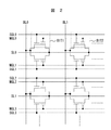
本発明のメモリセルにより、メモリアレイを構成したときの等価回路を図2に示した。ここでは、ワード線(SGL)を共通にするセルなど、8ビットを示している。これを繰り返すことで、アレイが構成される。図の例では、メモリセル(BIT1、BIT2等)が8個配置され、ビット線(BL0、BL1)とこれに交差するワード線(SGL0、SGL1、SGL2、SGL3)、及びメモリゲートがつながる線(以下、メモリゲート線の略称する:MGL0、MGL1、MGL2、MGL3)が配置されている。SL0、SL1はソース線である。 FIG. 2 shows an equivalent circuit when a memory array is constituted by the memory cells of the present invention. Here, 8 bits are shown for cells that share a word line (SGL). By repeating this, an array is formed. In the example shown in the figure, eight memory cells (BIT1, BIT2, etc.) are arranged, and bit lines (BL0, BL1), word lines (SGL0, SGL1, SGL2, SGL3) intersecting with these, and lines (memory lines) are connected. Hereinafter, abbreviated memory gate lines: MGL0, MGL1, MGL2, and MGL3) are arranged. SL0 and SL1 are source lines.
図3、図4は、等価回路図と、このメモリアレイを実現するための、半導体基板上での、平面配置(レイアウト)を示したものである。平面レイアウト図では、セル配置を説明する為、活性領域1150と選択ゲート1500、及びメモリゲート1550とコンタクト配置1650のみを示した。但し、後の形成工程で説明するように、メモリゲートは自己整合プロセスにより形成できるため、形成工程で図示したようなマスクは存在せず、配置を説明するためのものである。一点鎖線で囲む領域が、等価回路図のWORD1に対応した2ビットである。図3の等価回路図を対照すれば、ビット線BL1を中心に左右に一対の選択ゲート1500及びメモリゲート1550が配置されている。
3 and 4 show an equivalent circuit diagram and a planar arrangement (layout) on a semiconductor substrate for realizing this memory array. In the plan layout diagram, only the
図5、図6は同様に、メモリゲートと選択ゲートの配置を入れ替えた場合の構成例の等価回路図、及びその平面レイアウトを示したものである。図7、図8は、全てのメモリセルの拡散層にkンタクトを設けた例である。活性領域をストライプ状に形成することができる。 5 and 6 similarly show an equivalent circuit diagram of a configuration example when the arrangement of the memory gate and the selection gate is switched, and a planar layout thereof. 7 and 8 are examples in which k tacts are provided in the diffusion layers of all the memory cells. The active region can be formed in a stripe shape.
図9、図10は、メモリセルを縦積みに配置した例を示し、各々等価回路図及び平面レイアウト図である。図10には、図9におけるBIT1の部分の選択ゲート1500及びメモリゲート1550の配置を示している。そして、この例の場合、セルは各ビット毎に繰り返すことになる。
9 and 10 show an example in which memory cells are arranged vertically, and are an equivalent circuit diagram and a planar layout diagram, respectively. FIG. 10 shows the arrangement of the
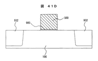
以上、メモリセルの各種の形態を例示したが、いずれのレイアウトにおいても、選択ゲートとメモリゲートの基本単位では、同じ構成となる。そこで図11に示したような基本構造で、形成プロセスについて説明する。
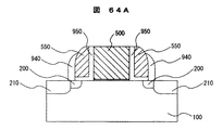
図11のレイアウトにより形成したメモリセルの断面構造を図12に示した。図11に見られるように、平面的には、活性領域1150の上部に選択ゲート1500とメモリゲート1550が並置される構成となっている。こうした構成を具現化した例が図12である。半導体基板100上にゲート絶縁膜が900および950を介して、選択ゲート500、メモリゲート550が形成される。これらの選択ゲート500、メモリゲート550の各々の一方の側壁に側面スペーサ940が形成される。選択ゲート500とメモリゲート550とは、やはりゲート絶縁膜950の延在部によって絶縁されている。符号950の部分は電荷保持部であり、例えばシリコン酸化膜とシリコン窒化膜とシリコン酸化膜を積層したものである。図中、積層膜での詳細な積層構造は省略している。メモリゲート側に拡散層200および210が形成される。ここでは、説明のため、この拡散層をソースと呼ぶことにする。選択ゲート側に拡散層300および310が形成される。ここでは、この拡散層をドレインと呼ぶことにする。本例では、拡散層210及び拡散層310は、側面スペーサ940と自己整合的に形成されている。
As described above, various types of memory cells have been exemplified. However, in any layout, the basic unit of the selection gate and the memory gate has the same configuration. Therefore, the formation process will be described with the basic structure as shown in FIG.
FIG. 12 shows a cross-sectional structure of the memory cell formed by the layout of FIG. As can be seen from FIG. 11, in a plan view, the
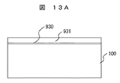
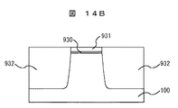
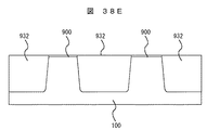
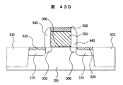
図13Aから図20Cまでは、本発明の第1の実施例である半導体装置をその製造工程順に示した模式的な断面図である。これらの図において、図11のチャネル方向での断面(A−A断面)を各図A(例えば、図13A、図14Aなど)、選択ゲートを含む断面(B−B断面)を各図B(例えば、図13B、図14Bなど)、メモリゲートを含む断面(C−C断面)を各図C(例えば、図13C、図14Cなど)に示す。ここでは、いわゆる0.13ミクロン世代相当のプロセスを用いて説明する。 FIGS. 13A to 20C are schematic cross-sectional views showing the semiconductor device according to the first embodiment of the present invention in the order of its manufacturing steps. In these drawings, a cross section (AA cross section) in the channel direction of FIG. 11 is shown in FIG. A (for example, FIG. 13A, FIG. 14A, etc.), and a cross section including a selection gate (BB cross section) is shown in FIG. For example, FIG. 13B, FIG. 14B, etc.) and a cross section including the memory gate (C-C cross section) is shown in each figure C (for example, FIG. 13C, FIG. 14C, etc.). Here, description will be made using a process equivalent to the so-called 0.13 micron generation.
半導体基板100の活性領域表面に10nmの酸化膜930を形成した後、シリコン窒化膜931を100nmCVD法により堆積する。この後、リソグラフィ技術を用いて、前記シリコン窒化膜931、及び酸化膜930の積層膜、及び半導体基板100を300nmエッチングし、活性領域(図11、1150に相当する)を所望形状にパターニングを行う(図13A、図13B、図13C)。
After a 10
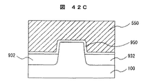
前記の工程で形成した溝の表面を酸化した後、シリコン酸化膜932を堆積させた。尚、半導体基板表面の酸化膜は、複雑になるので、図では表示を省略した。こうして準備した半導体基板表面を、化学機械的研磨(CMP:Chemical mechanical polishing)を行い、いわゆる浅溝アイソレーション(STI: Shallow Trench Isolation)を完成させる(図14A、図14B、図14C)。
After oxidizing the surface of the groove formed in the above step, a
窒化膜931をマスクとして、酸化膜932を50nmエッチングすることで、凸型の形状を得ることができる。このエッチングとして、ウエット系エッチングを用いることで、基板へのダメージを与えないようにすることが出来る(図15A、図15B、図15C)。
A convex shape can be obtained by etching the
これまで、マスクとして用いて来た窒化膜931及び酸化膜930を除去することで、活性領域のシリコン表面を露出させる(図16A、図16B、図16C)。
By removing the
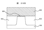
半導体基板表面を熱酸化により、2.5nmのゲート絶縁膜900を形成した後、多結晶シリコン500をCVD(Chemical Vapour Deposition)法により200nm堆積、更にシリコン酸化膜935を50nm堆積する。選択ゲートパターン(図11、1500)によりパターニングしたのち、該酸化膜935および多結晶シリコン500をエッチングし、選択ゲート電極を形成する。このとき(c)に示したように、メモリゲート領域では、凸型側面に500等が残らないように加工を行う(図17A、図17B、図17C)。
After a 2.5 nm
メモリゲート領域のゲート絶縁膜900を除去した後、露出した基板表面を4nm酸化する。この上部に、CVD法によりシリコン窒化膜を8nm、更にシリコン酸化膜7nmを堆積することで、ONO膜950を形成する。このONO膜950の形成においては、ISSG(In-Situ Steam Generation)酸化を用いることが出来る。即ち、基板表面をISSG酸化することで、酸化膜を5nm成長させ、シリコン窒化膜を14nm堆積する。この後、該シリコン窒化膜をISSG酸化することで、上部酸化膜6nmを形成することができる。
After removing the
ONO膜950を形成した後、高濃度にリンをin-situでドーピングした多結晶シリコンを70nm堆積する。そして、この多結晶シリコン膜に対して、異方性エッチングを行うことで、選択ゲート500側面にスペーサ形状のメモリゲート550を形成する。この時、コンタクト形成部には、ホトレジストパターンによりマスクをおくことができる(図18A、図18B、図18C)。又、ここでは図示していないが、不要部分の凸型側面から多結晶シリコン550を除くように、追加エッチングを行うことができる。
After the
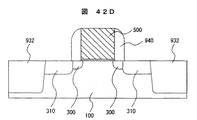
不要部分となる多結晶シリコン550をエッチング除去する。不要部分となる多結晶シリコン層は、具体的には、選択ゲート500のメモリゲートとなる領域と反対側面の多結晶シリコン層である。このときONO膜950を下地保護層として用いることができる。選択ゲート500およびメモリゲート550をマスクに砒素をイオン打ち込みすることで、ソース200およびドレイン300を形成する(図19A、図19B、図19C)。
The
露出したONO膜950をエッチング除去し、次いで、それぞれ選択ゲート500およびメモリゲート550をマスクに砒素をイオン打ち込みすることで、ソース200及びドレイン300を形成することにより、イオン打ち込み時の加速エネルギーを低くし、浅い接合を作ることができる。又、この時、イオン打ち込みに対する表面保護層として、基板上で3nmの熱酸化膜を形成してもよい。また、この熱酸化工程でISSG酸化法を用いることで、ONO積層膜の窒化膜側面にも酸化膜を形成し、窒化膜外周に窒化膜-酸化膜の良好な界面を持つ構造を得ることができる。
The exposed
更に、シリコン酸化膜を100nm堆積し、このシリコン酸化膜を異方性エッチングすることで、選択ゲート500及びメモリゲート550側面にスペーサ940を形成する。更に、これをマスクに、拡散層210及び拡散層310を砒素のイオン打ち込み法により形成する(図20A、図20B、図20C)。これらの不純物ドーピングにあわせて選択ゲート500にも不純物をドーピングすることが出来る。これらのプロセスは通常のLDD(Lightly doped drain)プロセスを適用したものである。以下通常のCMOSプロセスの配線工程をとることで、メモリセルが形成される。
Further, a silicon oxide film is deposited to a thickness of 100 nm, and this silicon oxide film is anisotropically etched to form spacers 940 on the side surfaces of the
<実施の形態2>
前述の形成プロセスを、より安定したプロセスとした例を図21Aから図25Cに示した。これらの図においても、上述の実施例と同様に、図11に示したそれぞれの断面を用いている。即ち、各図A、B、Cは上述の例と同様の断面を示す。
<
An example in which the above-described formation process is a more stable process is shown in FIGS. 21A to 25C. In these drawings as well, the respective cross sections shown in FIG. 11 are used as in the above-described embodiment. That is, each figure A, B, C shows the same cross section as the above-mentioned example.
前述の実施の形態1において、図16A、16B、16Cの段階まで形成した後、ゲート絶縁膜900を形成する。更に、多結晶シリコン500を300nm堆積し、CMP法により、この多結晶シリコンを研磨することで、多結晶シリコン500表面を平坦化する。活性領域の凸部頂上において、200nmの厚さになるようにする。その後、50nmのシリコン酸化膜935を堆積する。選択ゲートパターン(図11、符号1500)を用いて、酸化膜935、多結晶シリコン500をエッチングし、選択ゲートを形成する(図21A、図21B、図21C)。
In
メモリゲート550となる多結晶シリコンを堆積したのち、スペーサ加工を行うことで、メモリゲートを形成する(図22A、図22B、図22C)。
After depositing polycrystalline silicon to be the
不要部分となるメモリゲート層550を除去し、メモリゲート550及び選択ゲート900と自己整合的に拡散層200及び拡散層300をイオン打ち込みにより形成する(図23A、図23B、図23C)。
The
酸化膜スペーサ940形成を行い、更に拡散層210及び拡散層310を形成する(図24A、図24B、図24C)。
An
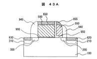
既知のいわゆるサリサイド(SALICIDE)プロセスを用いて、拡散層210、310、及び選択ゲート500とメモリゲート550の上部を選択的にシリサイド化する(図25A、図25B、図25C)。形成されたシリサイド層が600、620、630、650である。
このプロセスでは、選択ゲート上面が平坦化されているため、加工が容易になる。
The upper part of the diffusion layers 210 and 310 and the
In this process, since the upper surface of the selection gate is flattened, processing becomes easy.
<実施の形態3>
拡散層200、210、300、310を形成するイオン打ち込み時に、基板面に対して斜方から打ち込むことで、有効な拡散層を形成することが出来る。即ち、活性領域が凸型をしているため、斜めからイオン注入することで、側面に不純物を導入することができる。図26は斜めからのイオン注入の状態の例を示す断面図である。この例では、半導体基板100に酸化膜932が設けられている。図26に示すように2方向(A、B)から打ち込むことにより、凸部領域の両側面に沿った領域を有する拡散層200が形成されている。
<
When ions are implanted to form the diffusion layers 200, 210, 300, and 310, an effective diffusion layer can be formed by implanting the substrate surface obliquely. That is, since the active region is convex, impurities can be introduced into the side surface by ion implantation from an oblique direction. FIG. 26 is a cross-sectional view showing an example of the state of ion implantation from an oblique direction. In this example, an
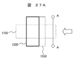
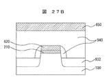
<実施の形態4及び5>
図27A及び図27Bは、サリサイド工程で、良好な接合特性を得る構造を説明したものである。図27Aは、平面レイアウトである。図27Aでは、図11と同様に符号1150は活性領域、1500は選択ゲート、1550はメモリゲートである。図27Bは、図27AのA−A断面を矢印で示した方向から見たセル構造を示したものである。半導体基板100の凸型側面にスペーサ940を形成することで、凸型上部のみにシリサイド層620が形成されるようにしたものである。シリサイド620は、拡散層210内に形成することができる。尚、図において、符号932は酸化膜、650はシリサイド層である。
<Embodiments 4 and 5>
27A and 27B illustrate a structure for obtaining good bonding characteristics in the salicide process. FIG. 27A is a planar layout. In FIG. 27A, as in FIG. 11,
本例では、活性領域1150が、断面構造が凸型形状をとっている為、この段差部にメモリゲート550がスペーサ状に残ることが考えられる。図28から図36は、この段差について説明する為の図である。
In this example, since the
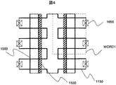
図28はメモリセルアレイの等価回路図、図29はその主要部の平面配置を示した図である。図28のWORD1として示したメモリアレー領域の平面配置が、図29に示される。メモリアレー領域WORD1内のメモリセルBIT1及びBIT2が、図29の平面図のWORD1内に示される。BIT1及びBIT2の各々のメモリセルにおける選択ゲート1500、メモリゲート1550が、図の左右に線対称に配置されている。領域1150が活性領域、符号1650がコンタクトを示すことはこれまでの例と同様である。本例では、対向するメモリゲートが同相で駆動される例である。
FIG. 28 is an equivalent circuit diagram of the memory cell array, and FIG. 29 is a diagram showing a planar arrangement of main parts thereof. FIG. 29 shows a planar arrangement of the memory array area shown as WORD1 in FIG. Memory cells BIT1 and BIT2 in the memory array region WORD1 are shown in WORD1 in the plan view of FIG. The
前述した製造工程から分かるように、メモリゲート1550の加工時には、活性領域1150の断面構造が凸型になっている。その為、符号1555で示した領域に活性領域1150段差に沿って、加工残りが発生する。選択ゲート1500を挟んで、メモリゲート1550の反対側では、メモリゲートの除去が行われているため、こうした加工残りは発生しない。図29からわかるように、この加工残り1555は、メモリゲート1550に付随する形になる為、メモリゲート間での短絡を起こすことはない。
As can be seen from the manufacturing process described above, the cross-sectional structure of the
そのため、図30に示すように、メモリゲート550をスペーサ加工する際、オーバーエッチングすることなく加工することで、図29に示した加工残りの領域1555を形成することが出来る。従って、メモリゲートの抵抗を低減することができる。尚、図30A、図30B、及び図30Cは、これまでと同様に、図11の各断面に対応させている。
Therefore, as shown in FIG. 30, when the
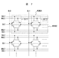
図31、図32はその他のアレイ構成例を示したものである。図31は等価回路図、図32はその主要部の平面配置を示した図である。この例では、メモリゲートMGLは共通化した例である。その他に部分はこれまでの例と同様であるので、詳細説明は省略する。本例は、スプリットゲート構造のセルのため、セルの選択は選択ゲートにより行うことができるため取り得る構成である。図32には、図31におけるWORD1部の2つのメモリセルBIT1、BIT2の部分が示される。各部の符号はこれまでと同様である。図32の例では、メモリゲート1550間をつなぐように加工残り1555が発生する。しかし、メモリゲートが共通化されているため、メモリゲート間での短絡による不良を発生させることなく、抵抗低減することができる。
31 and 32 show other examples of the array configuration. FIG. 31 is an equivalent circuit diagram, and FIG. 32 is a diagram showing a planar arrangement of the main part. In this example, the memory gate MGL is a common example. Since other parts are the same as the previous examples, detailed description thereof is omitted. In this example, since the cell has a split gate structure, the cell can be selected by a selection gate. FIG. 32 shows a portion of two memory cells BIT1 and BIT2 in the WORD1 portion in FIG. The symbols of each part are the same as before. In the example of FIG. 32, a
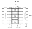
対向セルのメモリゲートのみ共通化したのが図33、図34の例である。図33は等価回路図、図34はその主要部の平面配置を示した図である。この例では、対向するメモリゲートは共通化(MGL0、MGL1)した例である。共通化したメモリゲートMGL0、MGL1に対応する領域が、図34の左右に示される。更に、共通化したメモリゲートMGL0に対応する領域は、図33に見られる、MGL0が接続する二つのメモリゲートが左右対称に符号1550として図示される。共通化したメモリゲートMGL0に対応するワード線SGL0、SGL1が、前記符号1550の部分に平行に設けられている。又、共通化したメモリゲートMGL1に対応する領域は、図33に見られる、MGL1が接続する二つのメモリゲートが左右対称に符号1550として図示される。共通化したメモリゲートMGL1に対応するワード線SGL2、SGL3に関してMGL0の場合と同様に図示される。その他に部分はこれまでの例と同様であるので、詳細説明は省略する。
Only the memory gates of the counter cells are shared in the example of FIGS. FIG. 33 is an equivalent circuit diagram, and FIG. 34 is a diagram showing a planar arrangement of the main part. In this example, the opposing memory gates are common (MGL0, MGL1). Regions corresponding to the shared memory gates MGL0 and MGL1 are shown on the left and right in FIG. Further, in the region corresponding to the shared memory gate MGL0, two memory gates to which MGL0 is connected as shown in FIG. Word lines SGL0 and SGL1 corresponding to the shared memory gate MGL0 are provided in parallel with the
このセルでは、対向するメモリゲートが共通化されているため、図34中に符号1555で示した加工残りは問題を起こすことはない。符号1551は選択ゲートのメモリゲートとは反対側に形成されたスペーサ550を除去するマスク配置例を示したものである。
In this cell, since the opposing memory gates are shared, the processing residue indicated by
本実施例においては、メモリゲート部の素子分離酸化膜をエッチングにより、基板表面から後退させているので、メモリゲート電極が形成される活性領域が凸形状となっている。そのため、メモリゲート電極を形成したときに、メモリゲート電極材が凸形状の側面にも形成される。これによって、メモリゲート電極を有するトランジスタの実効的なチャネル幅が、活性領域を凸形状としないときと比べて増大する。一方、周辺デバイスが形成されるの活性領域を凸形状とすると、側面にもチャネルが形成され、凸形状の側面と凸形状の上面とでチャネルが形成される閾値が異なる。そのため、ゲート電極に従来のオフ状態となる電圧を印加したときに、凸形状の側面にチャネルが形成されてしまう。これにより、オフ状態であっても、側面チャネルに起因するリーク電流が流れてしまい好ましくない。 In this embodiment, since the element isolation oxide film in the memory gate portion is recessed from the substrate surface by etching, the active region where the memory gate electrode is formed has a convex shape. Therefore, when the memory gate electrode is formed, the memory gate electrode material is also formed on the convex side surface. Thereby, the effective channel width of the transistor having the memory gate electrode is increased as compared with the case where the active region is not convex. On the other hand, when the active region in which the peripheral device is formed has a convex shape, a channel is also formed on the side surface, and the threshold value at which the channel is formed differs between the convex side surface and the convex upper surface. Therefore, a channel is formed on the convex side surface when a conventional voltage for turning off is applied to the gate electrode. Thereby, even in the off state, a leakage current caused by the side surface channel flows, which is not preferable.
そのため、本実施例では、メモリゲート部の素子分離酸化膜のみをエッチングすることによって、周辺デバイスの活性領域には凸形状を形成せずにメモリゲート電極が形成される活性領域を凸形状とした。 Therefore, in this embodiment, by etching only the element isolation oxide film in the memory gate portion, the active region where the memory gate electrode is formed is formed in a convex shape without forming the convex shape in the active region of the peripheral device. .
本実施例では、メモリゲート部の素子分離絶縁膜がエッチングするプロセスを有しているので、メモリゲート部の素子分離絶縁膜の表面は、選択ゲート電極を有するトランジスタおよび周辺デバイスが形成される素子分離絶縁膜の表面よりも低くなっている。 In this embodiment, since the element isolation insulating film in the memory gate portion has a process of etching, the surface of the element isolation insulating film in the memory gate portion is an element on which a transistor having a select gate electrode and a peripheral device are formed. It is lower than the surface of the isolation insulating film.
<実施の形態6>
縦積みしたメモリセルをしめしたのが図35、図36の例である。図33は等価回路図、図34はその主要部の平面配置を示した図である。
<
FIG. 35 and FIG. 36 show examples of vertically stacked memory cells. FIG. 33 is an equivalent circuit diagram, and FIG. 34 is a diagram showing a planar arrangement of the main part.
縦積みした場合、必ず片側のスペーサゲート550を除去するため、スペーサ加工時にオーバーエッチングしなくても、加工残りによる短絡等の問題をおこすことはない。
When stacked vertically, the
次にメモリゲートのみ凸型形状をとった例を説明する。図37Aから図43Eは、その他の実施例を製造工程順に示した素子の断面図である。この例の場合、選択ゲートと同時に周辺回路やロジック部には、通常の平坦型デバイスを形成できる。周辺回路で用いるデバイスは、回路設計上、デバイスパラメータが変わらないことが求められる。これにより、他で設計したものをそのまま用いることができるためである。そのため、周辺回路でのデバイスは、これまでと同じものができることが求められる場合がある。そのため、通常構造のデバイスができることが求められ、本発明実施例が有効である。 Next, an example in which only the memory gate has a convex shape will be described. FIG. 37A to FIG. 43E are cross-sectional views of elements showing other examples in the order of manufacturing steps. In the case of this example, an ordinary flat device can be formed in the peripheral circuit and the logic portion simultaneously with the selection gate. The device used in the peripheral circuit is required to have the same device parameter in terms of circuit design. This is because other designs can be used as they are. Therefore, there are cases where it is required that devices in the peripheral circuit can be the same as before. Therefore, it is required that a device having a normal structure can be formed, and the embodiment of the present invention is effective.
尚、図37Aから図43Eにおいては、これまでと同様に、図11のチャネル方向での断面(A−A断面)を各A図、選択ゲートを含む断面(B−B断面)を各B図、メモリゲートを含む断面(C−C断面)を各C図に示す。更に、各D図は、周辺デバイスのチャネル方向断面、各E図は、周辺デバイスのゲートを含む断面を示したものである。ここで、周辺デバイスは等価回路に示されてはいないが、通例の集積回路構成が用いて十分であり、各図の断面図は前記主要部の断面を取り出して示したものである。以下の例においても、周辺デバイスに言及したものは同様の断面を示している。 In FIGS. 37A to 43E, as in the past, the cross section in the channel direction (AA cross section) in FIG. 11 is shown in each A figure, and the cross section including the selection gate (BB cross section) in each B figure. A cross section including a memory gate (C-C cross section) is shown in each C diagram. Further, each D diagram shows a cross section of the peripheral device in the channel direction, and each E diagram shows a cross section including the gate of the peripheral device. Here, although the peripheral device is not shown in an equivalent circuit, a usual integrated circuit configuration is sufficient, and the cross-sectional views of each figure show a cross section of the main part. Also in the following examples, reference to peripheral devices shows similar cross sections.
前述の浅溝アイソレーションプロセスにより、半導体基板に素子分離構造を形成する(図37A、図37B、図37C、図37D、図37E)。即ち、半導体基板100の活性領域表面に酸化膜930を形成した後、シリコン窒化膜931を堆積する。この後、リソグラフィ技術を用いて、前記シリコン窒化膜931、及び酸化膜930の積層膜、及び半導体基板100の所望部分をエッチングし、活性領域を形成する。前記の工程で形成した溝の表面を酸化した後、シリコン酸化膜932を堆積させた。尚、半導体基板表面の酸化膜は、複雑になるので、図では表示を省略した。こうして準備した半導体基板表面を、化学機械的研磨を行い、いわゆる浅溝アイソレーションを完成させる。
An element isolation structure is formed on the semiconductor substrate by the shallow trench isolation process described above (FIGS. 37A, 37B, 37C, 37D, and 37E). That is, after forming the
露出した基板表面を熱酸化することで、2.5nmのゲート絶縁膜900を形成する(図38A、図38B、図38C、図38D、図38E)。
By thermally oxidizing the exposed substrate surface, a 2.5 nm
多結晶シリコン500を堆積し、パターニングすることで、選択ゲートを形成する(図39A、図39B、図39C、図39D、図39E)。このとき、周辺回路部におけるデバイスのゲート電極を同時に形成することができる。 The selection gate is formed by depositing and patterning polycrystalline silicon 500 (FIGS. 39A, 39B, 39C, 39D, and 39E). At this time, the gate electrode of the device in the peripheral circuit portion can be formed simultaneously.
選択ゲートおよび周辺デバイス部をレジスト800でマスクする(図40A、図40B、図40C、図40D、図40E)。 The selection gate and the peripheral device portion are masked with a resist 800 (FIGS. 40A, 40B, 40C, 40D, and 40E).
メモリゲート部の素子分離酸化膜932を50nmエッチングする(図41A、図41B、図41C、図41D、図41E)。
The element
メモリゲートのゲート絶縁膜950を形成したのち、スペーサの形成プロセスによりメモリゲート550を形成する。次いで、イオン打ち込み法により、拡散層200、210、300、310を形成する(図42A、図42B、図42C、図42D、図42E)。これらのプロセスは前述の実施例と同様に行うことができる。
After forming the
通例のサリサイドプロセスを適用し、シリサイド化部分を形成した構造を示している(図43A、図43B、図43C、図43D、図43E)。 A structure in which a silicide portion is formed by applying a usual salicide process is shown (FIGS. 43A, 43B, 43C, 43D, and 43E).
尚、図43Fに、図43Eの符号Zの部分の部分拡大図を示す。図43Eまでの図では、半導体基板面は直線で描かれているが、実際の工程では、図43Fのように、シリコン酸化膜の形成は、シリコンの凸部の端部に若干のくぼみが形成されることになる。特にことわりはないが、本例以外でも、この状況は同様である。 FIG. 43F shows a partially enlarged view of the portion indicated by the symbol Z in FIG. 43E. In the drawings up to FIG. 43E, the surface of the semiconductor substrate is drawn with a straight line. However, in the actual process, as shown in FIG. 43F, the formation of the silicon oxide film forms a slight depression at the end of the silicon protrusion. Will be. This situation is the same except for this example, although there is no particular notice.
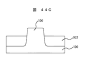
<実施の形態7>
図44A−Eは、前記発明実施例において、凸型形状を形成する際、メモリ部でもマスクすることで、歩留まりを向上させる例を示したものである。即ち、図40A−Eにおけるマスク800をメモリ部の選択ゲート側にも配置(符号801の部分がこのマスクに相当する)することで、選択ゲート拡散層300、310が凸形状にならないようにすることが出来る。これにより、メモリアレイ内であっても、周辺回路領域と拡散層も同じ構造を得ることができる。
<
44A to 44E show examples in which the yield is improved by masking even the memory portion when forming the convex shape in the embodiment of the present invention. That is, by arranging the
<実施の形態8>
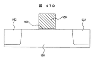
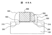
図45A−Eから図48A−Eは、その他の実施例を示す図で、選択ゲートおよび周辺回路デバイスを平坦に形成し、メモリゲートを凸型上に形成する工程を示したものである。図45A−Eから図48A−Eにおいては、これまでと同様に各A−Cは、図11のチャネル方向での各断面、更に、各D図、各E図は、周辺デバイスのチャネル方向断面及び周辺デバイスのゲートを含む断面を示したものである。以下、基本的な工程は、これまでの例と同様であるので、基本工程は簡潔に説明し、本例固有の事項を詳述する。
<Eighth embodiment>
45A to 48A to 48A to 48E show other embodiments, and show the process of forming the selection gate and the peripheral circuit device flat and forming the memory gate on the convex shape. 45A-E to 48A-E, each AC is a cross section in the channel direction of FIG. 11, and each D figure and each E figure are cross sections in the channel direction of the peripheral devices. And a cross section including gates of peripheral devices. Hereinafter, since the basic process is the same as that of the previous examples, the basic process will be briefly described, and details specific to this example will be described in detail.
これまでの例と同様に、半導体基板100に素子分離領域を形成する(図45A、図45B、図45C、図45D、図45E)。 As in the previous examples, element isolation regions are formed in the semiconductor substrate 100 (FIGS. 45A, 45B, 45C, 45D, and 45E).
周辺回路領域及び選択ゲート領域にマスク802を置き、メモリゲート部に凸型形状を形成する(図46A、図46B、図46C、図46D、図46E)。
A
選択ゲート500及び周辺回路デバイスを加工する(図47A、図47B、図47C、図47D、図47E)。
The
メモリゲート絶縁膜950及びメモリゲート550を形成し、以下、前述の実施例と同様の加工プロセスを行うことで、メモリセルおよび周辺回路デバイスを得ることができる(図48A、図48B、図48C、図48D、図48E)。このプロセスにより、周辺回路領域及び選択ゲートには通常のMOSFETが形成でき、メモリゲートは凸型活性領域を持つものにすることが出来る。又、図46A−Eの工程で、レジストで周辺部のみを覆うようにすることで、選択ゲートおよびメモリゲートを、凸型活性領域上に形成することができる。
The memory
<実施の形態9>
本発明の記憶装置においては、図1に見られるように、選択トランジスタとメモリゲートは、2つのトランジスタが縦積みされた構造とみることが出来る。ここでセルの読み出し電流を考えると、等価的には選択ゲートに対応する抵抗Rcgと、メモリゲートに対応する抵抗Rmgが直列に接続されたものとみることができる。これを等価回路として示したのが図49である。その為、上記メモリゲートのみを凸型とした場合、Rmgを小さくすることが出来る。
<
In the memory device of the present invention, as shown in FIG. 1, the selection transistor and the memory gate can be regarded as a structure in which two transistors are stacked vertically. Considering the read current of the cell, it can be considered that the resistor Rcg corresponding to the selection gate and the resistor Rmg corresponding to the memory gate are connected in series. FIG. 49 shows this as an equivalent circuit. Therefore, when only the memory gate is convex, Rmg can be reduced.
そこで、前記従来読み出し法とは逆に、V1<V2とすることで、大きな読み出し電流を得ることができる。選択ゲートでは表面に形成されていた反転層から、凸型形状により、基板内部にキャリアを引き込むことができるためである。 Therefore, contrary to the conventional reading method, a large read current can be obtained by setting V1 <V2. This is because, in the select gate, carriers can be drawn into the substrate from the inversion layer formed on the surface by a convex shape.
前記凸形状による効果はSOI(Silicon On Insulator)上に形成されたメモリセルでも得ることができる。図50は平面レイアウト、図51は、その断面構造を示したものである。 The effect of the convex shape can be obtained even in a memory cell formed on an SOI (Silicon On Insulator). FIG. 50 shows a planar layout, and FIG. 51 shows its cross-sectional structure.
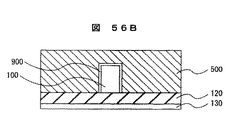
平面レイアウトでの特徴は、レイアウトされるチャネル幅をバルクに比べ小さく出来ることである。断面構造では、支持基板130上に埋め込み酸化膜120がおかれていることである。図52A−Cから図56A−Cは製造工程順にその素子の断面図を示すものである。これらの図において、各A図は、図50に示したように、チャネル方向断面(A−A断面)、各B図は選択ゲートを含む断面(B−B断面)、各C図はメモリゲートを含む断面(C−C断面)を示したものである。
A feature of the planar layout is that the channel width to be laid out can be made smaller than that of the bulk. In the cross-sectional structure, the buried
支持基板130上の、いわゆる「埋め込み酸化膜」120上にある80nmの厚さのシリコン単結晶(SOI)100を、活性領域パターン(図50、符号1150)によりエッチングする(図52A、図52B、図52C)。
An 80 nm thick silicon single crystal (SOI) 100 on a so-called “buried oxide film” 120 on the
SOI100表面を酸化し、2.5nmのゲート絶縁膜900を形成する。多結晶シリコン500を300nm堆積したのち、CMP法で研磨し、多結晶シリコン表面を平坦化する。更に、CVD法によりシリコン酸化膜935を50nm堆積した後、選択ゲートパターン(図50、符号1500)を用いて、酸化膜935と多結晶シリコン500の積層膜をエッチングする(図53A、図53B、図53C)。
The surface of the
メモリゲート領域のシリコン表面を露出させ、熱酸化することで4nmの酸化膜を形成し、10nmの厚さのシリコン窒化膜及び7nmのシリコン酸化膜を積層することで、メモリゲート絶縁膜950を形成する(図54A、図54B、図54C)。
The silicon surface of the memory gate region is exposed and thermally oxidized to form a 4 nm oxide film, and a 10 nm thick silicon nitride film and a 7 nm silicon oxide film are stacked to form a memory
多結晶シリコンを50nm堆積したのち、スペーサ加工プロセスを用いることで選択ゲート側面にスペーサゲート550を形成し(図55A)、不要部分の多結晶シリコンを除去する(図55A、図55B、図55C)。
After depositing polycrystalline silicon by 50 nm, spacer processing is used to form a
前述した実施例と同様にして、拡散層200、210、300、310を形成することで、凸型形状をしたメモリセル構造を得ることができる(図56A、図56B、図56C)。 By forming the diffusion layers 200, 210, 300, and 310 in the same manner as in the above-described embodiment, a convex memory cell structure can be obtained (FIGS. 56A, 56B, and 56C).
<実施の形態10>
図57A−Cから図61A−Cに、前記SOIを用いて凸型形状セルを形成する際、容易に加工できるプロセスを示した。これらの各図でも図50の各断面を用いている。
<Embodiment 10>
57A-C to FIG. 61A-C show a process that can be easily processed when forming a convex shaped cell using the SOI. In each of these drawings, each cross section of FIG. 50 is used.
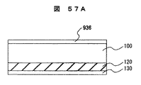
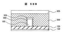
SOI基板表面のシリコン(SOI)を熱酸化し30nmの厚さの酸化膜層936を形成する。その後、活性領域パターン(図50、符号1150)を用いて酸化膜936及びSOI層を加工する(図57A、図57B、図57C)。
(図58) SOI100側面を酸化し2.5nmのゲート絶縁膜900を形成する。多結晶シリコン500を300nm堆積したのち、CMP法で研磨し、多結晶シリコン表面を平坦化する。さらに、CVD法によりシリコン酸化膜935を50nm堆積した後、選択ゲートパターン(図50、1500)を用いて、酸化膜935と多結晶シリコン500の積層膜(図58A)をエッチングする(図58A、図58B、図58C)。この際、層936によりSOI100はエッチングされることがない。
Silicon (SOI) on the surface of the SOI substrate is thermally oxidized to form an
(FIG. 58) The side surface of
メモリゲート領域のシリコン表面を露出させ、熱酸化することで4nmの酸化膜を形成し、10nmの厚さのシリコン窒化膜及び7nmのシリコン酸化膜を積層することで、メモリゲート絶縁膜950(図59A)を形成する(図59A、図59B、図59C)。 The silicon surface of the memory gate region is exposed and thermally oxidized to form a 4 nm oxide film, and a 10 nm thick silicon nitride film and a 7 nm silicon oxide film are stacked to form a memory gate insulating film 950 (FIG. 59A) (FIGS. 59A, 59B, and 59C).
多結晶シリコンを50nm堆積した後、スペーサ加工プロセスを用いることで選択ゲート500の側面にスペーサゲート550を形成し、不要部分の多結晶シリコンを除去する(図60A、図60B、図60C)。
After depositing polycrystalline silicon by 50 nm, a
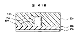
前述した実施例と同様にして、拡散層200、210、300、310を形成することで、凸型形状をしたメモリセル構造を得ることができる(図61A、図61B、図61C)。 By forming the diffusion layers 200, 210, 300, and 310 in the same manner as in the above-described embodiment, a memory cell structure having a convex shape can be obtained (FIGS. 61A, 61B, and 61C).
メモリゲートでは、ゲート絶縁膜950が選択ゲートのゲート絶縁膜900に比べ厚いため、駆動力に劣るものになっている。しかし、この構造では、メモリゲートはSOIの上部及び両側面をチャネルとすることができるため、選択ゲートとの電流駆動力比を小さくすることができる。
In the memory gate, since the
<実施の形態11>
これまで、メモリゲートを選択ゲートの片側にのみ形成するメモリセル構造について説明してきたが、本例は、選択ゲートの両側にメモリゲートをもつ構造でも有効である。
<Embodiment 11>
The memory cell structure in which the memory gate is formed only on one side of the selection gate has been described so far, but this example is also effective in a structure having memory gates on both sides of the selection gate.
図62に、その平面レイアウトを示した。選択ゲート1500の両側にメモリゲート1550が配置されている。但し、メモリゲートを自己整合プロセスで形成する場合には、マスクパターンとしてはメモリゲートは存在しない。図63A−Cは、図62の素子断面構造を示したものである。図63Aは、図62のチャネル方向(A−A断面)での断面図、図63Bは、選択ゲートを含む図62のB−B断面、図63Cはメモリゲートを含む図62のC−C及びD−D断面である。C−C断面とD−D断面では、同じ構造が形成されている。図21A−Cから図25A−Cにおいて示した製法で、図23A−Cで説明した不要部分のメモリゲート550除去工程を変え、選択ゲートの両側にメモリゲートが形成されるようにすればよい。本実施例では、選択ゲートおよび両メモリゲートが凸型形状上に形成されている。
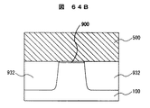
FIG. 62 shows the planar layout.
図64は、図62および図63で説明したメモリセル構造で、選択ゲートは平坦構造で形成し、メモリゲートが凸型形状で形成されているものである。図37A−Cから図43A−Cにおいて説明した製造工程を用いることで形成することができる。 FIG. 64 shows the memory cell structure described with reference to FIGS. 62 and 63, in which the selection gate is formed in a flat structure and the memory gate is formed in a convex shape. It can be formed by using the manufacturing process described in FIGS. 37A to 43A to 43A-C.
<実施の形態12>
図65、図66A−Cは、SOIを用いて選択ゲートの両側にメモリゲートを形成する場合を示したものである。
<
65 and 66A-C show the case where memory gates are formed on both sides of the selection gate using SOI.
図65に、その平面レイアウトを示した。選択ゲート1500の両側にメモリゲート1550が配置されている。ただし、メモリゲートを自己整合プロセスで形成する場合には、マスクパターンとしてはメモリゲートは存在しない。図66A−Cは図65の素子断面構造を示したものである。図66Aは、図62のチャネル方向(A−A断面)での断面図、図66Bは、選択ゲートを含む図65のB−B断面、図66Cはメモリゲートを含む図65のC−C及びD−D断面である。C−C断面とD−D断面では、同じ構造が形成されている。図21A−Cから図25A−Cにおいて示した製法で、図23A−Cで説明した不要部分のメモリゲート550除去工程を変え、選択ゲートの両側にメモリゲートが形成されるようにすればよい。本実施例では、選択ゲート及び両メモリゲートがSOIで作られた凸型形状上に形成することができる。
FIG. 65 shows the planar layout.
本願発明の主な諸形態を列挙する。 The main aspects of the present invention will be listed.
第1の例は、シリコン基板上に形成された、第1の絶縁ゲート型電界効果トランジスタと、該トランジスタゲートと並行に、かつ接して形成された第2の絶縁ゲート型電界効果トランジスタを持ち、これらゲートと直行する方向に第1の拡散層電極と、第1のゲートと該ゲートにより制御された第1のチャネルと、第2のゲートと該ゲートに制御された第2のチャネルと、第2の拡散層電極が置かれ、第2の絶縁ゲート型電界効果トランジスタのゲート絶縁膜が電荷保持機能をもち、第1の拡散層と第2の拡散層間を流れる電流を、第2のゲートによる電圧特性を変化させる不揮発性半導体記憶装置において、第1のトランジスタのチャネルが、第1の拡散層電極と第2の拡散層電極をむすぶチャネル方向に直行する方向に凸型に形成され、該凸部の側面をチャネルとして用いていることを特徴とする半導体記憶装置。 The first example has a first insulated gate field effect transistor formed on a silicon substrate, and a second insulated gate field effect transistor formed in parallel with and in contact with the transistor gate, A first diffusion layer electrode in a direction perpendicular to the gates, a first gate, a first channel controlled by the gate, a second gate, a second channel controlled by the gate, 2 diffusion layer electrodes are placed, the gate insulating film of the second insulated gate field effect transistor has a charge holding function, and the current flowing between the first diffusion layer and the second diffusion layer is caused by the second gate. In the nonvolatile semiconductor memory device that changes the voltage characteristics, the channel of the first transistor is formed in a convex shape in a direction perpendicular to the channel direction extending between the first diffusion layer electrode and the second diffusion layer electrode, A semiconductor memory device using a side surface of a convex portion as a channel.
第2の例は、シリコン基板上に形成された、第1の絶縁ゲート型電界効果トランジスタと、該トランジスタゲートと並行に、かつ接して形成された第2の絶縁ゲート型電界効果トランジスタを持ち、これらゲートと直行する方向に第1の拡散層電極と、第1のゲートと該ゲートにより制御された第1のチャネルと、第2のゲートと該ゲートに制御された第2のチャネルと、第2の拡散層電極が置かれ、第2の絶縁ゲート型電界効果トランジスタのゲート絶縁膜が電荷保持機能をもち、第1の拡散層と第2の拡散層間を流れる電流を、第2のゲートによる電圧特性を変化させる不揮発性半導体記憶装置において、第2のトランジスタのチャネルが、第1の拡散層電極と第2の拡散層電極をむすぶチャネル方向に直行する方向に凸型に形成され、該凸部の側面をチャネルとして用いていることを特徴とする半導体記憶装置。 The second example has a first insulated gate field effect transistor formed on a silicon substrate, and a second insulated gate field effect transistor formed in parallel with and in contact with the transistor gate, A first diffusion layer electrode in a direction perpendicular to the gates, a first gate, a first channel controlled by the gate, a second gate, a second channel controlled by the gate, 2 diffusion layer electrodes are placed, the gate insulating film of the second insulated gate field effect transistor has a charge holding function, and the current flowing between the first diffusion layer and the second diffusion layer is caused by the second gate. In the nonvolatile semiconductor memory device that changes the voltage characteristics, the channel of the second transistor is formed in a convex shape in a direction perpendicular to the channel direction extending between the first diffusion layer electrode and the second diffusion layer electrode, A semiconductor memory device using a side surface of a convex portion as a channel.
第3の例は、シリコン基板上に形成された、第1の絶縁ゲート型電界効果トランジスタと、該トランジスタゲートと並行に、かつ接して形成された第2の絶縁ゲート型電界効果トランジスタを持ち、これらゲートと直行する方向に第1の拡散層電極と、第1のゲートと該ゲートにより制御された第1のチャネルと、第2のゲートと該ゲートに制御された第2のチャネルと、第2の拡散層電極が置かれ、第2の絶縁ゲート型電界効果トランジスタのゲート絶縁膜が電荷保持機能をもち、第1の拡散層と第2の拡散層間を流れる電流を、第2のゲートによる電圧特性を変化させる不揮発性半導体記憶装置において、第1と第2のトランジスタのチャネルが、第1の拡散層電極と第2の拡散層電極をむすぶチャネル方向に直行する方向に凸型に形成され、前記凸部の側面をチャネルとして用いていることを特徴とする半導体記憶装置。 The third example has a first insulated gate field effect transistor formed on a silicon substrate, and a second insulated gate field effect transistor formed in parallel with and in contact with the transistor gate, A first diffusion layer electrode in a direction perpendicular to the gates, a first gate, a first channel controlled by the gate, a second gate, a second channel controlled by the gate, 2 diffusion layer electrodes are placed, the gate insulating film of the second insulated gate field effect transistor has a charge holding function, and the current flowing between the first diffusion layer and the second diffusion layer is caused by the second gate. In a non-volatile semiconductor memory device that changes voltage characteristics, the channels of the first and second transistors are formed in a convex shape in a direction perpendicular to the channel direction extending between the first diffusion layer electrode and the second diffusion layer electrode. Is, the semiconductor memory device is characterized in that using the side surface of the convex portion as a channel.
第4の例は、シリコン基板上に形成された、第1の絶縁ゲート型電界効果トランジスタと、該トランジスタゲートと並行に、かつ接して形成された第2の絶縁ゲート型電界効果トランジスタを持ち、これらゲートと直行する方向に第1の拡散層電極と、第1のゲートと該ゲートにより制御された第1のチャネルと、第2のゲートと該ゲートに制御された第2のチャネルと、第2の拡散層電極が置かれ、第2の絶縁ゲート型電界効果トランジスタのゲート絶縁膜が電荷保持機能をもち、第1の拡散層と第2の拡散層間を流れる電流を、第2のゲートによる電圧特性を変化させる不揮発性半導体記憶装置において、第1のトランジスタのチャネルは平坦な基板面をチャネルとし、第2のトランジスタのチャネルが、第1の拡散層電極と第2の拡散層電極をむすぶチャネル方向に直行する方向に凸型に形成され、前記凸部の側面をチャネルとして用いていることを特徴とする半導体記憶装置。 The fourth example has a first insulated gate field effect transistor formed on a silicon substrate, and a second insulated gate field effect transistor formed in parallel with and in contact with the transistor gate, A first diffusion layer electrode in a direction perpendicular to the gates, a first gate, a first channel controlled by the gate, a second gate, a second channel controlled by the gate, 2 diffusion layer electrodes are placed, the gate insulating film of the second insulated gate field effect transistor has a charge holding function, and the current flowing between the first diffusion layer and the second diffusion layer is caused by the second gate. In the nonvolatile semiconductor memory device in which the voltage characteristics are changed, the channel of the first transistor has a flat substrate surface as the channel, and the channel of the second transistor has the first diffusion layer electrode and the second diffusion layer. A semiconductor memory device, characterized in that it is formed in a convex shape in a direction perpendicular to the channel direction passing through the electrodes, and the side surface of the convex portion is used as a channel.
第5の例は、一つの基板の上に、複数の前記第1の例なる半導体記憶装置と、絶縁膜を介してチャネルを制御する電界効果型トランジスタを持ち、少なくとも1つの電界効果型トランジスタのチャネルが平坦であることを特徴とする、集積半導体装置。 The fifth example has a plurality of the semiconductor memory devices of the first example and a field effect transistor that controls a channel through an insulating film on one substrate, and includes at least one field effect transistor. An integrated semiconductor device, wherein a channel is flat.
第6の例は、一つの基板の上に、複数の前記第2の例なる半導体記憶装置と、絶縁膜を介してチャネルを制御する電界効果型トランジスタを持ち、少なくとも1つの電界効果型トランジスタのチャネルが平坦であることを特徴とする、集積半導体装置。 The sixth example has a plurality of semiconductor memory devices of the second example and a field effect transistor that controls a channel through an insulating film on one substrate, and includes at least one field effect transistor. An integrated semiconductor device, wherein a channel is flat.
第7の例は、一つの基板の上に、複数の前記第3の例なる半導体記憶装置と、絶縁膜を介してチャネルを制御する電界効果型トランジスタを持ち、少なくとも1つの電界効果型トランジスタのチャネルが平坦であることを特徴とする、集積半導体装置。 The seventh example has a plurality of the semiconductor memory devices of the third example and a field effect transistor that controls a channel through an insulating film on one substrate, and includes at least one field effect transistor. An integrated semiconductor device, wherein a channel is flat.
第8の例は、一つの基板の上に、複数の前記第4の例なる半導体記憶装置と、絶縁膜を介してチャネルを制御する電界効果型トランジスタを持ち、少なくとも1つの電界効果型トランジスタのチャネルが平坦であることを特徴とする、集積半導体装置。 The eighth example has a plurality of the semiconductor memory devices of the fourth example and a field effect transistor that controls a channel through an insulating film on one substrate, and includes at least one field effect transistor. An integrated semiconductor device, wherein a channel is flat.
第9の例は、前記第3の例なる半導体記憶装置と、絶縁膜を介してチャネルを制御する電界効果型トランジスタを持つ集積半導体装置の形成工程において、素子分離領域を形成する工程と、少なくとも1つの該電界効果トランジスタを覆う工程と、該マスクにより該半導体記憶装置のチャネル部を凸型形状に加工する工程を持つことを特徴とする半導体記憶装置の形成法。 A ninth example includes a step of forming an element isolation region in the step of forming an integrated semiconductor device having the semiconductor memory device of the third example and a field effect transistor that controls a channel through an insulating film, A method for forming a semiconductor memory device, comprising: covering one field effect transistor; and processing a channel portion of the semiconductor memory device into a convex shape with the mask.
第10の例は、前記第4の例なる半導体記憶装置の形成工程において、第1のゲート電極を形成した後、該第1のゲート電極をマスクにエッチングをする工程を持ち、第2のトランジスタのチャネルを凸型形状とする工程を持つことを特徴とする半導体記憶装置の形成法。 The tenth example includes the step of forming the first gate electrode in the step of forming the semiconductor memory device of the fourth example and then etching using the first gate electrode as a mask. A method for forming a semiconductor memory device, comprising the step of:
以上詳細に説明した通り、本発明方式は、現行の半導体プロセスのみを用いて、より性能の高い半導体装置を得ることができるため、高い利用可能性を持つ。 As described above in detail, the method of the present invention has high applicability because a semiconductor device with higher performance can be obtained using only the current semiconductor process.
100、130:基板、120:酸化膜、200、210、300、310:拡散層電極、500、550:ゲート電極、600,620、630、650,655:シリサイド層、900、950:ゲート絶縁膜、930、931、932、935、936、940:絶縁膜層、800、801、802:レジスト、1500:選択ゲートパターン、1150:活性領域パターン、1550:メモリゲート配置、1551:スペーサエッチングマスクパターン、1555:加工残り、1650:コンタクトパターン。 100, 130: substrate, 120: oxide film, 200, 210, 300, 310: diffusion layer electrode, 500, 550: gate electrode, 600, 620, 630, 650, 655: silicide layer, 900, 950: gate insulating film , 930, 931, 932, 935, 936, 940: insulating film layer, 800, 801, 802: resist, 1500: selection gate pattern, 1150: active region pattern, 1550: memory gate arrangement, 1551: spacer etching mask pattern, 1555: processing residue, 1650: contact pattern.
Claims (9)
前記半導体基板上に形成された、第1の絶縁ゲート型電界効果トランジスタと、
前記半導体基板上に形成され且つ前記第1の絶縁ゲート型電界効果トランジスタの有する第1のゲート電極と絶縁膜を介して形成された第2のゲート電極を有する第2の絶縁ゲート型電界効果トランジスタと、を有し、
前記第1及び第2の絶縁ゲート型電界効果トランジスタの各ゲート電極と交差する方向に、
第1の拡散層電極と、
前記第1の絶縁ゲート型電界効果トランジスタの有する第1のゲート電極と当該第1のゲート電極に対応する第1のチャネル領域と、
前記第2の絶縁ゲート型電界効果トランジスタの有する第2のゲート電極と当該第2のゲート電極に対応する第2のチャネル領域と、
前記第1の拡散層電極と、前記第1のチャネル領域と第2のチャネル領域を挟んで対向する第2の拡散層電極と、を有し、
前記第2の絶縁ゲート型電界効果トランジスタのゲート絶縁膜は、電荷保持機能を有し、
前記第2のゲート電極による電圧特性の変化の寄与によって、前記第1の拡散層電極と前記第2の拡散層電極との間を流れる電流を制御し、且つ
前記第1の拡散層電極と前記第2の拡散層電極を結ぶチャネル方向に交差する方向に凸型半導体領域を有し、
前記第1の絶縁ゲート型電界効果トランジスタの有する第1のチャネル領域が、前記凸型半導体領域の側壁に形成されることを特徴とする半導体装置。 A semiconductor substrate;
A first insulated gate field effect transistor formed on the semiconductor substrate;
A second insulated gate field effect transistor having a first gate electrode formed on the semiconductor substrate and having a first gate electrode of the first insulated gate field effect transistor and a second gate electrode formed through an insulating film And having
In a direction crossing each gate electrode of the first and second insulated gate field effect transistors,
A first diffusion layer electrode;
A first gate electrode of the first insulated gate field effect transistor and a first channel region corresponding to the first gate electrode;
A second gate electrode of the second insulated gate field effect transistor and a second channel region corresponding to the second gate electrode;
A first diffusion layer electrode; and a second diffusion layer electrode facing the first channel region and the second channel region,
The gate insulating film of the second insulated gate field effect transistor has a charge holding function,
The current flowing between the first diffusion layer electrode and the second diffusion layer electrode is controlled by the contribution of the change in voltage characteristics by the second gate electrode, and the first diffusion layer electrode and the A convex semiconductor region in a direction intersecting the channel direction connecting the second diffusion layer electrodes;
A semiconductor device, wherein a first channel region of the first insulated gate field effect transistor is formed on a sidewall of the convex semiconductor region.
前記半導体基板上に形成された、第1の絶縁ゲート型電界効果トランジスタと、
前記半導体基板上に形成され且つ前記第1の絶縁ゲート型電界効果トランジスタの有する第1のゲート電極と絶縁膜を介して形成された第2のゲート電極を有する第2の絶縁ゲート型電界効果トランジスタと、を有し、
前記第1及び第2の絶縁ゲート型電界効果トランジスタの各ゲート電極と交差する方向に、
第1の拡散層電極と、
前記第1の絶縁ゲート型電界効果トランジスタの有する第1のゲート電極と当該第1のゲート電極に対応する第1のチャネル領域と、
前記第2の絶縁ゲート型電界効果トランジスタの有する第2のゲート電極と当該第2のゲート電極に対応する第2のチャネル領域と、
前記第1の拡散層電極と、前記第1のチャネル領域と第2のチャネル領域を挟んで対向する第2の拡散層電極と、を有し、
前記第2の絶縁ゲート型電界効果トランジスタのゲート絶縁膜は、電荷保持機能を有し、
前記第2のゲート電極による電圧特性の変化の寄与によって、前記第1の拡散層電極と前記第2の拡散層電極との間を流れる電流を制御し、且つ
前記第1の拡散層電極と前記第2の拡散層電極を結ぶチャネル方向に交差する方向に凸型半導体領域を有し、
前記第2の絶縁ゲート型電界効果トランジスタの有する第2のチャネル領域が、前記凸型半導体領域の側壁に形成されることを特徴とする半導体装置。 A semiconductor substrate;
A first insulated gate field effect transistor formed on the semiconductor substrate;
A second insulated gate field effect transistor having a first gate electrode formed on the semiconductor substrate and having a first gate electrode of the first insulated gate field effect transistor and a second gate electrode formed through an insulating film And having
In a direction crossing each gate electrode of the first and second insulated gate field effect transistors,
A first diffusion layer electrode;
A first gate electrode of the first insulated gate field effect transistor and a first channel region corresponding to the first gate electrode;
A second gate electrode of the second insulated gate field effect transistor and a second channel region corresponding to the second gate electrode;
A first diffusion layer electrode; and a second diffusion layer electrode facing the first channel region and the second channel region,
The gate insulating film of the second insulated gate field effect transistor has a charge holding function,
The current flowing between the first diffusion layer electrode and the second diffusion layer electrode is controlled by the contribution of the change in voltage characteristics by the second gate electrode, and the first diffusion layer electrode and the A convex semiconductor region in a direction intersecting the channel direction connecting the second diffusion layer electrodes;
A semiconductor device, wherein a second channel region of the second insulated gate field effect transistor is formed on a sidewall of the convex semiconductor region.
前記半導体基板に形成された第1素子分離酸化膜と、
前記半導体基板に形成された第2素子分離酸化膜と、
前記半導体基板上に、第1絶縁膜を介して形成された第1ゲート電極と、
前記半導体基板上に、第2絶縁膜を介して形成された、前記第1ゲート電極に隣接する第2ゲート電極とを有し、
前記第2絶縁膜は、電荷蓄積膜を有し、
前記第1ゲート電極は、前記第1素子分離酸化膜上に形成され、
前記第2ゲート電極は、前記第2素子分離絶縁膜上に形成され、
前記第2素子分離絶縁膜の表面は、前記第1素子分離酸化膜の表面よりも後退していることを特徴とする半導体装置。 A semiconductor substrate;
A first element isolation oxide film formed on the semiconductor substrate;
A second element isolation oxide film formed on the semiconductor substrate;
A first gate electrode formed on the semiconductor substrate via a first insulating film;
A second gate electrode adjacent to the first gate electrode formed on the semiconductor substrate via a second insulating film;
The second insulating film has a charge storage film,
The first gate electrode is formed on the first element isolation oxide film,
The second gate electrode is formed on the second element isolation insulating film,
The surface of the second element isolation insulating film is recessed from the surface of the first element isolation oxide film.
更に、前記半導体基板に形成された第3素子分離酸化膜と、
前記半導体基板上に、第3絶縁膜を介して形成された第3ゲート電極とを有し、
前記第3ゲート電極は、前記第3素子分離酸化膜上に形成され、
前記第2素子分離酸化膜の表面は、前記第3素子分離酸化膜の表面よりも後退していることを特徴とする半導体装置。 The semiconductor device according to claim 6.
A third element isolation oxide film formed on the semiconductor substrate;
A third gate electrode formed on the semiconductor substrate via a third insulating film;
The third gate electrode is formed on the third element isolation oxide film,
The surface of the second element isolation oxide film is recessed from the surface of the third element isolation oxide film.
前記第1ゲート電極および前記第2ゲート電極は、メモリアレー領域内に形成され、前記第3ゲート電極は、周辺回路領域内に形成されていることを特徴とする半導体装置。 The semiconductor device according to claim 7.
The semiconductor device, wherein the first gate electrode and the second gate electrode are formed in a memory array region, and the third gate electrode is formed in a peripheral circuit region.
Priority Applications (6)
| Application Number | Priority Date | Filing Date | Title |
|---|---|---|---|
| JP2004221764A JP2006041354A (en) | 2004-07-29 | 2004-07-29 | Semiconductor device and its manufacturing method |
| TW094120881A TWI360865B (en) | 2004-07-29 | 2005-06-22 | Semiconductor device and manufacturing method of s |
| US11/182,013 US7504689B2 (en) | 2004-07-29 | 2005-07-15 | Semiconductor device and manufacturing method of semiconductor device |
| KR1020050064173A KR20060050209A (en) | 2004-07-29 | 2005-07-15 | Semiconductordevice and manufacturing method of semiconductordevice |
| CN200510086030XA CN1728401B (en) | 2004-07-29 | 2005-07-20 | Semiconductor device and manufacturing method of semiconductor device |
| US12/368,538 US7847343B2 (en) | 2004-07-29 | 2009-02-10 | Semiconductor device and manufacturing method of semiconductor device |
Applications Claiming Priority (1)
| Application Number | Priority Date | Filing Date | Title |
|---|---|---|---|
| JP2004221764A JP2006041354A (en) | 2004-07-29 | 2004-07-29 | Semiconductor device and its manufacturing method |
Publications (2)
| Publication Number | Publication Date |
|---|---|
| JP2006041354A true JP2006041354A (en) | 2006-02-09 |
| JP2006041354A5 JP2006041354A5 (en) | 2007-04-05 |
Family
ID=35731149
Family Applications (1)
| Application Number | Title | Priority Date | Filing Date |
|---|---|---|---|
| JP2004221764A Pending JP2006041354A (en) | 2004-07-29 | 2004-07-29 | Semiconductor device and its manufacturing method |
Country Status (5)
| Country | Link |
|---|---|
| US (2) | US7504689B2 (en) |
| JP (1) | JP2006041354A (en) |
| KR (1) | KR20060050209A (en) |
| CN (1) | CN1728401B (en) |
| TW (1) | TWI360865B (en) |
Cited By (34)
| Publication number | Priority date | Publication date | Assignee | Title |
|---|---|---|---|---|
| JP2007281091A (en) * | 2006-04-04 | 2007-10-25 | Renesas Technology Corp | Semiconductor device, and manufacturing method thereof |
| JP2008263034A (en) * | 2007-04-11 | 2008-10-30 | Oki Electric Ind Co Ltd | Method for manufacturing semiconductor memory |
| JP2009049097A (en) * | 2007-08-16 | 2009-03-05 | Oki Electric Ind Co Ltd | Semiconductor nonvolatile memory cell and manufacturing method thereof, and semiconductor nonvolatile memory having the semiconductor nonvolatile memory cell and manufacturing method thereof |
| JP2011049580A (en) * | 2010-10-18 | 2011-03-10 | Renesas Electronics Corp | Semiconductor device |
| JP2011119331A (en) * | 2009-12-01 | 2011-06-16 | Renesas Electronics Corp | Method of manufacturing semiconductor integrated circuit device |
| US8154075B2 (en) | 2009-02-03 | 2012-04-10 | Renesas Electronics Corporation | Nonvolatile semiconductor memory device and method for manufacturing the same |
| JP2014017343A (en) * | 2012-07-09 | 2014-01-30 | Renesas Electronics Corp | Semiconductor device and manufacturing method of the same |
| JP2016004822A (en) * | 2014-06-13 | 2016-01-12 | ルネサスエレクトロニクス株式会社 | Semiconductor device |
| JP2016507908A (en) * | 2013-03-14 | 2016-03-10 | シリコン ストーリッジ テクノロージー インコーポレイテッドSilicon Storage Technology, Inc. | Nonvolatile memory cell having increased channel region effective width and method of manufacturing the same |
| JP2016051738A (en) * | 2014-08-28 | 2016-04-11 | ルネサスエレクトロニクス株式会社 | Semiconductor device manufacturing method |
| JP5982055B1 (en) * | 2015-12-18 | 2016-08-31 | 株式会社フローディア | MEMORY CELL, NONVOLATILE SEMICONDUCTOR MEMORY DEVICE, AND NONVOLATILE SEMICONDUCTOR MEMORY DEVICE MANUFACTURING METHOD |
| KR20170026172A (en) | 2015-08-26 | 2017-03-08 | 르네사스 일렉트로닉스 가부시키가이샤 | Semiconductor device |
| KR20170034345A (en) | 2015-09-18 | 2017-03-28 | 르네사스 일렉트로닉스 가부시키가이샤 | Semiconductor device |
| EP3188216A1 (en) | 2015-12-28 | 2017-07-05 | Renesas Electronics Corporation | Semiconductor device and manufacturing method thereof |
| US9741869B1 (en) | 2016-02-24 | 2017-08-22 | Renesas Electronics Corporation | Semiconductor device and method for manufacturing same |
| EP3208807A1 (en) | 2016-02-17 | 2017-08-23 | Renesas Electronics Corporation | Semiconductor device |
| US9899403B2 (en) | 2016-06-14 | 2018-02-20 | Renesas Electronics Corporation | Semiconductor device and method of manufacturing the same |
| JP2018056378A (en) * | 2016-09-29 | 2018-04-05 | ルネサスエレクトロニクス株式会社 | Semiconductor device and manufacturing method thereof |
| KR20180035129A (en) | 2016-09-28 | 2018-04-05 | 르네사스 일렉트로닉스 가부시키가이샤 | Semiconductor device and method of manufacturing semiconductor device |
| US10056402B2 (en) | 2016-09-30 | 2018-08-21 | Renesas Electronics Corporation | Semiconductor device |
| EP3407377A1 (en) | 2017-05-26 | 2018-11-28 | Renesas Electronics Corporation | Semiconductor device and manufacturing method for semiconductor device |
| US10163921B2 (en) | 2016-06-03 | 2018-12-25 | Renesas Electronics Corporation | Semiconductor device and manufacturing method of the same |
| CN109119423A (en) * | 2017-06-22 | 2019-01-01 | 瑞萨电子株式会社 | Semiconductor device and its manufacturing method |
| US10217759B2 (en) | 2016-09-30 | 2019-02-26 | Renesas Electronics Corporation | Semiconductor device |
| EP3454360A2 (en) | 2017-09-11 | 2019-03-13 | Renesas Electronics Corporation | Semiconductor device and manufacturing method therefor |
| EP3506333A2 (en) | 2017-12-27 | 2019-07-03 | Renesas Electronics Corporation | Semiconductor device and method of manufacturing the same |
| US10424591B2 (en) | 2017-09-19 | 2019-09-24 | Renesas Electronics Corporation | Semiconductor device and manufacturing method thereof |
| US10546946B2 (en) | 2016-02-24 | 2020-01-28 | Renesas Electronics Corporation | Method for manufacturing semiconductor device having thinned fins |
| US10854730B2 (en) | 2018-06-28 | 2020-12-01 | Renesas Electronics Corporation | Semiconductor device and method of manufacturing thereof |
| EP3823024A1 (en) | 2019-11-15 | 2021-05-19 | Renesas Electronics Corporation | Semiconductor device |
| US11101281B2 (en) | 2018-05-08 | 2021-08-24 | Renesas Electronics Corporation | Semiconductor device and method of manufacturing the same |
| US11183510B2 (en) | 2016-12-22 | 2021-11-23 | Renesas Electronics Corporation | Manufacturing method of semiconductor device and semiconductor device |
| US11205655B2 (en) | 2018-11-08 | 2021-12-21 | Renesas Electronics Corporation | Method for manufacturing semiconductor device including fin-structured transistor |
| US11302791B2 (en) | 2019-06-24 | 2022-04-12 | Renesas Electronics Corporation | Semiconductor device including a fin-type transistor and method of manufacturing the same |
Families Citing this family (26)
| Publication number | Priority date | Publication date | Assignee | Title |
|---|---|---|---|---|
| JP4601316B2 (en) * | 2004-03-31 | 2010-12-22 | ルネサスエレクトロニクス株式会社 | Nonvolatile semiconductor memory device |
| JP4659527B2 (en) * | 2005-06-20 | 2011-03-30 | ルネサスエレクトロニクス株式会社 | Manufacturing method of semiconductor device |
| KR100762262B1 (en) * | 2006-10-23 | 2007-10-01 | 삼성전자주식회사 | Nonvolatile memory device and method of forming the same |
| WO2008075656A1 (en) * | 2006-12-19 | 2008-06-26 | Nec Corporation | Semiconductor device |
| JP5404149B2 (en) * | 2009-04-16 | 2014-01-29 | ルネサスエレクトロニクス株式会社 | Semiconductor memory device |
| US8598646B2 (en) | 2011-01-13 | 2013-12-03 | Spansion Llc | Non-volatile FINFET memory array and manufacturing method thereof |
| US9966477B2 (en) | 2012-12-14 | 2018-05-08 | Cypress Semiconductor Corporation | Charge trapping split gate device and method of fabricating same |
| US9368606B2 (en) | 2012-12-14 | 2016-06-14 | Cypress Semiconductor Corporation | Memory first process flow and device |
| US20140167141A1 (en) | 2012-12-14 | 2014-06-19 | Spansion Llc | Charge Trapping Split Gate Embedded Flash Memory and Associated Methods |
| US9209197B2 (en) | 2012-12-14 | 2015-12-08 | Cypress Semiconductor Corporation | Memory gate landing pad made from dummy features |
| US20140167220A1 (en) * | 2012-12-14 | 2014-06-19 | Spansion Llc | Three dimensional capacitor |
| US10014380B2 (en) | 2012-12-14 | 2018-07-03 | Cypress Semiconductor Corporation | Memory first process flow and device |
| US8822289B2 (en) | 2012-12-14 | 2014-09-02 | Spansion Llc | High voltage gate formation |
| US8836006B2 (en) | 2012-12-14 | 2014-09-16 | Spansion Llc | Integrated circuits with non-volatile memory and methods for manufacture |
| US8816438B2 (en) | 2012-12-14 | 2014-08-26 | Spansion Llc | Process charging protection for split gate charge trapping flash |
| US20140167142A1 (en) | 2012-12-14 | 2014-06-19 | Spansion Llc | Use Disposable Gate Cap to Form Transistors, and Split Gate Charge Trapping Memory Cells |
| US20140210012A1 (en) | 2013-01-31 | 2014-07-31 | Spansion Llc | Manufacturing of FET Devices Having Lightly Doped Drain and Source Regions |
| JP2014232810A (en) * | 2013-05-29 | 2014-12-11 | ルネサスエレクトロニクス株式会社 | Semiconductor device and manufacturing method of the same |
| JP6274826B2 (en) * | 2013-11-14 | 2018-02-07 | ルネサスエレクトロニクス株式会社 | Semiconductor device and manufacturing method thereof |
| US9368644B2 (en) * | 2013-12-20 | 2016-06-14 | Cypress Semiconductor Corporation | Gate formation memory by planarization |
| CN106158637B (en) * | 2015-03-31 | 2019-04-26 | 中芯国际集成电路制造(上海)有限公司 | Fin formula field effect transistor and forming method thereof |
| CN106158638B (en) * | 2015-04-01 | 2019-03-29 | 中芯国际集成电路制造(上海)有限公司 | Fin formula field effect transistor and forming method thereof |
| CN105120143B (en) * | 2015-07-28 | 2019-03-29 | 深圳市理邦精密仪器股份有限公司 | The method and device of electronic colposcope elimination image spot |
| JP2017045947A (en) | 2015-08-28 | 2017-03-02 | ルネサスエレクトロニクス株式会社 | Semiconductor device and manufacturing method for semiconductor device |
| JP2018107317A (en) * | 2016-12-27 | 2018-07-05 | ルネサスエレクトロニクス株式会社 | Semiconductor device and semiconductor device manufacturing method |
| CN106981422B (en) * | 2017-03-01 | 2020-03-24 | 中国科学院微电子研究所 | Vertical TFET and manufacturing method thereof |
Citations (7)
| Publication number | Priority date | Publication date | Assignee | Title |
|---|---|---|---|---|
| JPH05275659A (en) * | 1992-03-30 | 1993-10-22 | Toshiba Corp | Non-volatile semiconductor memory device |
| JPH1022403A (en) * | 1996-06-28 | 1998-01-23 | Toshiba Corp | Nonvolatile semiconductor storage device |
| JP2001036048A (en) * | 1999-07-16 | 2001-02-09 | Denso Corp | Semiconductor memory and manufacture thereof |
| JP2002198532A (en) * | 2000-10-28 | 2002-07-12 | Samsung Electronics Co Ltd | Semiconductor device having effective width of expanded active region and its manufacturing method |
| WO2004023556A1 (en) * | 2002-09-05 | 2004-03-18 | Infineon Technologies Ag | Word and bit line arrangement for a finfet semiconductor memory |
| JP2004186452A (en) * | 2002-12-04 | 2004-07-02 | Renesas Technology Corp | Nonvolatile semiconductor memory device and its manufacturing method |
| WO2004059738A1 (en) * | 2002-12-20 | 2004-07-15 | Infineon Technologies Ag | Fin field effect transistor memory cell, fin field effect transistor memory cell arrangement, and method for the production of a fin field effect transistor memory cell |
Family Cites Families (8)
| Publication number | Priority date | Publication date | Assignee | Title |
|---|---|---|---|---|
| US5055716A (en) * | 1990-05-15 | 1991-10-08 | Siarc | Basic cell for bicmos gate array |
| US5604146A (en) * | 1996-06-10 | 1997-02-18 | Vanguard International Semiconductor Corporation | Method to fabricate a semiconductor memory device having an E-shaped storage node |
| US5969383A (en) * | 1997-06-16 | 1999-10-19 | Motorola, Inc. | Split-gate memory device and method for accessing the same |
| US6383861B1 (en) * | 1999-02-18 | 2002-05-07 | Micron Technology, Inc. | Method of fabricating a dual gate dielectric |
| JP3973819B2 (en) * | 1999-03-08 | 2007-09-12 | 株式会社東芝 | Semiconductor memory device and manufacturing method thereof |
| JP4068781B2 (en) * | 2000-02-28 | 2008-03-26 | 株式会社ルネサステクノロジ | Semiconductor integrated circuit device and method for manufacturing semiconductor integrated circuit device |
| EP1172856A1 (en) * | 2000-07-03 | 2002-01-16 | Matsushita Electric Industrial Co., Ltd. | Nonvolatile semiconductor memory device and method for fabricating the same |
| JP4904631B2 (en) * | 2000-10-27 | 2012-03-28 | ソニー株式会社 | Nonvolatile semiconductor memory device and manufacturing method thereof |
-
2004
- 2004-07-29 JP JP2004221764A patent/JP2006041354A/en active Pending
-
2005
- 2005-06-22 TW TW094120881A patent/TWI360865B/en not_active IP Right Cessation
- 2005-07-15 KR KR1020050064173A patent/KR20060050209A/en not_active Application Discontinuation
- 2005-07-15 US US11/182,013 patent/US7504689B2/en not_active Expired - Fee Related
- 2005-07-20 CN CN200510086030XA patent/CN1728401B/en not_active Expired - Fee Related
-
2009
- 2009-02-10 US US12/368,538 patent/US7847343B2/en active Active
Patent Citations (7)
| Publication number | Priority date | Publication date | Assignee | Title |
|---|---|---|---|---|
| JPH05275659A (en) * | 1992-03-30 | 1993-10-22 | Toshiba Corp | Non-volatile semiconductor memory device |
| JPH1022403A (en) * | 1996-06-28 | 1998-01-23 | Toshiba Corp | Nonvolatile semiconductor storage device |
| JP2001036048A (en) * | 1999-07-16 | 2001-02-09 | Denso Corp | Semiconductor memory and manufacture thereof |
| JP2002198532A (en) * | 2000-10-28 | 2002-07-12 | Samsung Electronics Co Ltd | Semiconductor device having effective width of expanded active region and its manufacturing method |
| WO2004023556A1 (en) * | 2002-09-05 | 2004-03-18 | Infineon Technologies Ag | Word and bit line arrangement for a finfet semiconductor memory |
| JP2004186452A (en) * | 2002-12-04 | 2004-07-02 | Renesas Technology Corp | Nonvolatile semiconductor memory device and its manufacturing method |
| WO2004059738A1 (en) * | 2002-12-20 | 2004-07-15 | Infineon Technologies Ag | Fin field effect transistor memory cell, fin field effect transistor memory cell arrangement, and method for the production of a fin field effect transistor memory cell |
Cited By (62)
| Publication number | Priority date | Publication date | Assignee | Title |
|---|---|---|---|---|
| JP2007281091A (en) * | 2006-04-04 | 2007-10-25 | Renesas Technology Corp | Semiconductor device, and manufacturing method thereof |
| US8530958B2 (en) | 2006-04-04 | 2013-09-10 | Renesas Electronics Corporation | Semiconductor device having split gate type, non-volatile memory cells and a method of manufacturing the same |
| JP2008263034A (en) * | 2007-04-11 | 2008-10-30 | Oki Electric Ind Co Ltd | Method for manufacturing semiconductor memory |
| JP2009049097A (en) * | 2007-08-16 | 2009-03-05 | Oki Electric Ind Co Ltd | Semiconductor nonvolatile memory cell and manufacturing method thereof, and semiconductor nonvolatile memory having the semiconductor nonvolatile memory cell and manufacturing method thereof |
| US8154075B2 (en) | 2009-02-03 | 2012-04-10 | Renesas Electronics Corporation | Nonvolatile semiconductor memory device and method for manufacturing the same |
| JP2011119331A (en) * | 2009-12-01 | 2011-06-16 | Renesas Electronics Corp | Method of manufacturing semiconductor integrated circuit device |
| JP2011049580A (en) * | 2010-10-18 | 2011-03-10 | Renesas Electronics Corp | Semiconductor device |
| JP2014017343A (en) * | 2012-07-09 | 2014-01-30 | Renesas Electronics Corp | Semiconductor device and manufacturing method of the same |
| JP2016507908A (en) * | 2013-03-14 | 2016-03-10 | シリコン ストーリッジ テクノロージー インコーポレイテッドSilicon Storage Technology, Inc. | Nonvolatile memory cell having increased channel region effective width and method of manufacturing the same |
| JP2016004822A (en) * | 2014-06-13 | 2016-01-12 | ルネサスエレクトロニクス株式会社 | Semiconductor device |
| JP2016051738A (en) * | 2014-08-28 | 2016-04-11 | ルネサスエレクトロニクス株式会社 | Semiconductor device manufacturing method |
| KR20170026172A (en) | 2015-08-26 | 2017-03-08 | 르네사스 일렉트로닉스 가부시키가이샤 | Semiconductor device |
| EP3144960A2 (en) | 2015-08-26 | 2017-03-22 | Renesas Electronics Corporation | Semiconductor device |
| US10043814B2 (en) | 2015-08-26 | 2018-08-07 | Renesas Electronics Corporation | Semiconductor substrate with a single protruding portion with multiple different widths and insulation thickness |
| US10062706B2 (en) | 2015-09-18 | 2018-08-28 | Renesas Electronics Corporation | Semiconductor device |
| KR20170034345A (en) | 2015-09-18 | 2017-03-28 | 르네사스 일렉트로닉스 가부시키가이샤 | Semiconductor device |
| US9780109B2 (en) | 2015-09-18 | 2017-10-03 | Renesas Electronics Corporation | Semiconductor device |
| JP2017112331A (en) * | 2015-12-18 | 2017-06-22 | 株式会社フローディア | Memory cell, nonvolatile semiconductor memory device, and method of manufacturing nonvolatile semiconductor memory device |
| JP5982055B1 (en) * | 2015-12-18 | 2016-08-31 | 株式会社フローディア | MEMORY CELL, NONVOLATILE SEMICONDUCTOR MEMORY DEVICE, AND NONVOLATILE SEMICONDUCTOR MEMORY DEVICE MANUFACTURING METHOD |
| US9735169B2 (en) | 2015-12-28 | 2017-08-15 | Renesas Electronics Corporation | Semiconductor device and manufacturing method thereof |
| EP3188216A1 (en) | 2015-12-28 | 2017-07-05 | Renesas Electronics Corporation | Semiconductor device and manufacturing method thereof |
| US9831258B2 (en) | 2015-12-28 | 2017-11-28 | Renesas Electronics Corporation | Semiconductor device and manufacturing method thereof |
| US10395742B2 (en) | 2016-02-17 | 2019-08-27 | Renesas Electronics Corporation | Semiconductor device |
| EP3208807A1 (en) | 2016-02-17 | 2017-08-23 | Renesas Electronics Corporation | Semiconductor device |
| JP2017147313A (en) * | 2016-02-17 | 2017-08-24 | ルネサスエレクトロニクス株式会社 | Semiconductor device |
| US10038102B2 (en) | 2016-02-24 | 2018-07-31 | Renesas Electronics Corporation | Semiconductor device and method for manufacturing same |
| CN107123652B (en) * | 2016-02-24 | 2023-06-06 | 瑞萨电子株式会社 | Semiconductor device and method for manufacturing the same |
| US11217682B2 (en) | 2016-02-24 | 2022-01-04 | Renesas Electronics Corporation | Method for manufacturing semiconductor device having thinned fins |
| US9899540B2 (en) | 2016-02-24 | 2018-02-20 | Renesas Electronics Corporation | Semiconductor device and method for manufacturing same |
| CN107123652A (en) * | 2016-02-24 | 2017-09-01 | 瑞萨电子株式会社 | Semiconductor device and the method for manufacturing semiconductor device |
| JP2017152505A (en) * | 2016-02-24 | 2017-08-31 | ルネサスエレクトロニクス株式会社 | Semiconductor device and manufacturing method of the same |
| US10546946B2 (en) | 2016-02-24 | 2020-01-28 | Renesas Electronics Corporation | Method for manufacturing semiconductor device having thinned fins |
| US9741869B1 (en) | 2016-02-24 | 2017-08-22 | Renesas Electronics Corporation | Semiconductor device and method for manufacturing same |
| US10163921B2 (en) | 2016-06-03 | 2018-12-25 | Renesas Electronics Corporation | Semiconductor device and manufacturing method of the same |
| US10325921B2 (en) | 2016-06-03 | 2019-06-18 | Renesas Electronics Corporation | Semiconductor device and manufacturing method of the same |
| US10229925B2 (en) | 2016-06-14 | 2019-03-12 | Renesas Electronics Corporation | Semiconductor device and method of manufacturing the same |
| US9899403B2 (en) | 2016-06-14 | 2018-02-20 | Renesas Electronics Corporation | Semiconductor device and method of manufacturing the same |
| TWI735623B (en) * | 2016-09-28 | 2021-08-11 | 日商瑞薩電子股份有限公司 | Method of manufacturing semiconductor device |
| US10153293B2 (en) | 2016-09-28 | 2018-12-11 | Renesas Electronics Corporation | Semiconductor device and method of manufacturing semiconductor device |
| KR20180035129A (en) | 2016-09-28 | 2018-04-05 | 르네사스 일렉트로닉스 가부시키가이샤 | Semiconductor device and method of manufacturing semiconductor device |
| US10522558B2 (en) | 2016-09-28 | 2019-12-31 | Renesas Electronics Corporation | Semiconductor device and method of manufacturing semiconductor device |
| JP2018056378A (en) * | 2016-09-29 | 2018-04-05 | ルネサスエレクトロニクス株式会社 | Semiconductor device and manufacturing method thereof |
| US10217759B2 (en) | 2016-09-30 | 2019-02-26 | Renesas Electronics Corporation | Semiconductor device |
| US10056402B2 (en) | 2016-09-30 | 2018-08-21 | Renesas Electronics Corporation | Semiconductor device |
| US11183510B2 (en) | 2016-12-22 | 2021-11-23 | Renesas Electronics Corporation | Manufacturing method of semiconductor device and semiconductor device |
| EP3407377A1 (en) | 2017-05-26 | 2018-11-28 | Renesas Electronics Corporation | Semiconductor device and manufacturing method for semiconductor device |
| US10580785B2 (en) | 2017-05-26 | 2020-03-03 | Renesas Electronics Corporation | Semiconductor device and manufacturing method for semiconductor device |
| CN109119423B (en) * | 2017-06-22 | 2023-08-22 | 瑞萨电子株式会社 | Semiconductor device and method for manufacturing the same |
| US10439032B2 (en) | 2017-06-22 | 2019-10-08 | Renesas Electronics Corporation | Semiconductor device and method of manufacturing same |
| CN109119423A (en) * | 2017-06-22 | 2019-01-01 | 瑞萨电子株式会社 | Semiconductor device and its manufacturing method |
| JP2019009209A (en) * | 2017-06-22 | 2019-01-17 | ルネサスエレクトロニクス株式会社 | Semiconductor device and method for manufacturing semiconductor device |
| US10622371B2 (en) | 2017-09-11 | 2020-04-14 | Renesas Electronics Corporation | Semiconductor device and manufacturing method therefor |
| EP3454360A2 (en) | 2017-09-11 | 2019-03-13 | Renesas Electronics Corporation | Semiconductor device and manufacturing method therefor |
| US10424591B2 (en) | 2017-09-19 | 2019-09-24 | Renesas Electronics Corporation | Semiconductor device and manufacturing method thereof |
| US10777688B2 (en) | 2017-12-27 | 2020-09-15 | Renesas Electronics Corporation | Semiconductor device and method of manufacturing the same |
| EP3506333A2 (en) | 2017-12-27 | 2019-07-03 | Renesas Electronics Corporation | Semiconductor device and method of manufacturing the same |
| US11101281B2 (en) | 2018-05-08 | 2021-08-24 | Renesas Electronics Corporation | Semiconductor device and method of manufacturing the same |
| US10854730B2 (en) | 2018-06-28 | 2020-12-01 | Renesas Electronics Corporation | Semiconductor device and method of manufacturing thereof |
| US11205655B2 (en) | 2018-11-08 | 2021-12-21 | Renesas Electronics Corporation | Method for manufacturing semiconductor device including fin-structured transistor |
| US11302791B2 (en) | 2019-06-24 | 2022-04-12 | Renesas Electronics Corporation | Semiconductor device including a fin-type transistor and method of manufacturing the same |
| EP3823024A1 (en) | 2019-11-15 | 2021-05-19 | Renesas Electronics Corporation | Semiconductor device |
| US11302828B2 (en) | 2019-11-15 | 2022-04-12 | Renesas Electronics Corporation | Semiconductor device |
Also Published As
| Publication number | Publication date |
|---|---|
| US7847343B2 (en) | 2010-12-07 |
| US7504689B2 (en) | 2009-03-17 |
| US20060022260A1 (en) | 2006-02-02 |
| TWI360865B (en) | 2012-03-21 |
| KR20060050209A (en) | 2006-05-19 |
| TW200625553A (en) | 2006-07-16 |
| CN1728401A (en) | 2006-02-01 |
| US20090152619A1 (en) | 2009-06-18 |
| CN1728401B (en) | 2011-05-25 |
Similar Documents
| Publication | Publication Date | Title |
|---|---|---|
| JP2006041354A (en) | Semiconductor device and its manufacturing method | |
| JP5116987B2 (en) | Integrated semiconductor nonvolatile memory device | |
| JP4521597B2 (en) | Semiconductor memory device and manufacturing method thereof | |
| JP4646837B2 (en) | Manufacturing method of semiconductor device | |
| US7602010B2 (en) | Multi-bit multi-level non-volatile memory device and methods of operating and fabricating the same | |
| JP4659527B2 (en) | Manufacturing method of semiconductor device | |
| JP5456036B2 (en) | Nonvolatile semiconductor memory device | |
| JP5734744B2 (en) | Semiconductor device and manufacturing method thereof | |
| JP5007017B2 (en) | Manufacturing method of semiconductor device | |
| TWI413261B (en) | Semiconductor device | |
| CN105448843B (en) | Method for manufacturing semiconductor device | |
| JP5086626B2 (en) | Nonvolatile semiconductor memory device and manufacturing method thereof | |
| JP2008538867A (en) | Array source line in NAND flash memory | |
| JP2009302269A (en) | Method of manufacturing semiconductor device, and semiconductor device | |
| JP6630582B2 (en) | Semiconductor device | |
| KR100608376B1 (en) | Non-volatile memory cell using state of three kinds and method of manufacturing the same | |
| KR100618877B1 (en) | Multi-bit non-volatile memory device, method of working the same, and method of fabricating the same | |
| US20070004142A1 (en) | Asymmetric operation method of non-volatile memory structure | |
| JP5014591B2 (en) | Semiconductor device and manufacturing method thereof | |
| US11302828B2 (en) | Semiconductor device | |
| JP4056964B2 (en) | Semiconductor device group, manufacturing method thereof, and semiconductor device | |
| CN114497073A (en) | Semiconductor device and method for manufacturing the same | |
| JP2008140898A (en) | Semiconductor device, and manufacturing method thereof | |
| JP5214700B2 (en) | Semiconductor device | |
| JP2011096727A (en) | Method of manufacturing semiconductor device |
Legal Events
| Date | Code | Title | Description |
|---|---|---|---|
| A521 | Request for written amendment filed |
Free format text: JAPANESE INTERMEDIATE CODE: A523 Effective date: 20070220 |
|
| A621 | Written request for application examination |
Free format text: JAPANESE INTERMEDIATE CODE: A621 Effective date: 20070220 |
|
| RD02 | Notification of acceptance of power of attorney |
Free format text: JAPANESE INTERMEDIATE CODE: A7422 Effective date: 20070220 |
|
| A977 | Report on retrieval |
Free format text: JAPANESE INTERMEDIATE CODE: A971007 Effective date: 20090917 |
|
| A131 | Notification of reasons for refusal |
Free format text: JAPANESE INTERMEDIATE CODE: A131 Effective date: 20090929 |
|
| A521 | Request for written amendment filed |
Free format text: JAPANESE INTERMEDIATE CODE: A523 Effective date: 20091130 |
|
| A711 | Notification of change in applicant |
Free format text: JAPANESE INTERMEDIATE CODE: A712 Effective date: 20100510 |
|
| A131 | Notification of reasons for refusal |
Free format text: JAPANESE INTERMEDIATE CODE: A131 Effective date: 20100706 |
|
| A02 | Decision of refusal |
Free format text: JAPANESE INTERMEDIATE CODE: A02 Effective date: 20101102 |