JP5014591B2 - Semiconductor device and manufacturing method thereof - Google Patents
Semiconductor device and manufacturing method thereof Download PDFInfo
- Publication number
- JP5014591B2 JP5014591B2 JP2005150304A JP2005150304A JP5014591B2 JP 5014591 B2 JP5014591 B2 JP 5014591B2 JP 2005150304 A JP2005150304 A JP 2005150304A JP 2005150304 A JP2005150304 A JP 2005150304A JP 5014591 B2 JP5014591 B2 JP 5014591B2
- Authority
- JP
- Japan
- Prior art keywords
- film
- region
- semiconductor device
- gate electrode
- insulating film
- Prior art date
- Legal status (The legal status is an assumption and is not a legal conclusion. Google has not performed a legal analysis and makes no representation as to the accuracy of the status listed.)
- Expired - Fee Related
Links
Images


Landscapes
- Semiconductor Memories (AREA)
- Non-Volatile Memory (AREA)
Description
本発明は、半導体装置及びその製造技術に関し、特に、不揮発性記憶素子を有する半導体装置に適用して有効な技術に関するものである。 The present invention relates to a semiconductor device and a manufacturing technique thereof, and more particularly to a technique effective when applied to a semiconductor device having a nonvolatile memory element.
半導体装置として、例えば、フラッシュメモリと呼称される不揮発性半導体記憶装置が知られている。このフラッシュメモリのメモリセルにおいては、1つの不揮発性素子で構成した1トランジスタ方式や、1つの不揮発性記憶素子と1つの選択用MISFET(Metal Insulator Semiconductor Field Effect Transistor)とで構成した2トランジスタ方式が知られている。また、不揮発性記憶素子においては、半導体基板と制御ゲート電極(コントロールゲート電極)との間の浮遊ゲート電極(フローティングゲート電極)に情報を記憶させる浮遊ゲート型や、半導体基板とゲート電極との間のゲート絶縁膜にON(窒化膜/酸化膜:Nitride/Oxide)膜を使用し、このゲート絶縁膜に情報を記憶させるMNOS(Metal Nitride Oxide Semiconductor)型や、半導体基板とゲート電極との間のゲート絶縁膜にONO(酸化膜/窒化膜/酸化膜:Oxide/Nitride/Oxide)膜を使用し、このゲート絶縁膜に情報を記憶させるMONOS(MetalOxide Nitride Oxide Semiconductor)型が知られている。 As a semiconductor device, for example, a nonvolatile semiconductor memory device called a flash memory is known. In the memory cell of this flash memory, a one-transistor method composed of one nonvolatile element or a two-transistor method composed of one nonvolatile memory element and one selection MISFET (Metal Insulator Semiconductor Field Effect Transistor). Are known. In the nonvolatile memory element, a floating gate type for storing information in a floating gate electrode (floating gate electrode) between the semiconductor substrate and the control gate electrode (control gate electrode), or between the semiconductor substrate and the gate electrode. MNOS (Metal Nitride Oxide Semiconductor) type that uses an ON (nitride / oxide) film as the gate insulating film and stores information in this gate insulating film, or between the semiconductor substrate and the gate electrode There is known a MONOS (Metal Oxide Nitride Oxide Semiconductor) type in which an ONO (oxide film / nitride film / oxide film: Oxide / Nitride / Oxide) film is used as a gate insulating film, and information is stored in the gate insulating film.
更に、不揮発性記憶素子においては、ゲート絶縁膜にONO膜を使用したMONOS型FETと、ゲート絶縁膜に通常の酸化シリコン膜を用いた制御用FET(パストランジスタ)とを等価回路的に直列接続し、MONOS型FETのゲート絶縁膜のみにホットエレクトロを注入させるスプリットゲート型不揮発性記憶素子が提案されている。
なお、本発明に関連する公知文献としては、例えば特開2004−221554号公報(特許文献1)、及び特開2001−168219号公報(特許文献2)がある。
Further, in the nonvolatile memory element, a MONOS type FET using an ONO film as a gate insulating film and a control FET (pass transistor) using a normal silicon oxide film as a gate insulating film are connected in series in an equivalent circuit. A split gate type nonvolatile memory element in which hot electro is injected only into the gate insulating film of the MONOS type FET has been proposed.
In addition, as a well-known document relevant to this invention, there exists Unexamined-Japanese-Patent No. 2004-221554 (patent document 1) and Unexamined-Japanese-Patent No. 2001-168219 (patent document 2), for example.
特許文献1には、スプリットゲート型不揮発性記憶素子が開示されている。また、同文献1には、ホットホールによる消去時に、選択ゲート電極(SG)に正の電圧を印加してチャネル電流を流すことにより、ホットエレクトロンとホットホールの注入位置をほぼ同じにする技術も開示されている。
特許文献2には、(1)電荷蓄積層の一部の誘電率を変えることで、基板ホットエレクトロン、2次衝突電離ホットエレクトロンなど基板と垂直方向に電荷を加速させて、MONOS型メモリトランジスタの動作電圧を低電圧化したまま書き込み速度の向上を実現する技術が開示されている。また、同文献2には、(2)チャネル形成領域に段差を形成することで、MONOS型メモリトランジスタの動作電圧を低電圧化したまま書き込み速度の向上を実現する技術も開示されている。
In
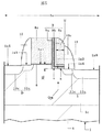
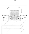
図25は、従来のスプリットゲート型不揮発性記憶素子の概略構成を示す模式的断面図である。図25において、符号101は半導体基板、符号102は例えば酸化膜からなるゲート絶縁膜、符号103はコントロールゲート電極、符号104は、例えばONO(酸化膜104a/窒化膜104b/酸化膜104c)膜からなるゲート絶縁膜、符号105はメモリゲート電極、符号Sはソース領域、符号Dはドレイン領域である。
FIG. 25 is a schematic cross-sectional view showing a schematic configuration of a conventional split gate nonvolatile memory element. In FIG. 25,
図25に示す不揮発性記憶素子は、半導体基板101上にゲート絶縁膜102を介在してコントロールゲート電極103が設けられ制御用FETと、半導体基板101上にゲート絶縁膜104を介在してメモリゲート電極105が設けられたMONOS型FETとを等価回路的に直列接続した構成になっている。
The nonvolatile memory element shown in FIG. 25 has a
この不揮発性記憶素子のデータ書き込みは、例えば、半導体基板101側から、メモリゲート電極105下のゲート絶縁膜104の窒化膜(電荷蓄積膜)104b中にホットエレクトロンを注入することによって行われる。一方、データ消去は、例えば、半導体基板101側から、メモリゲート電極105下のゲート絶縁膜104の窒化膜104b中にホットホールを注入して窒化膜104b中の電子を消去(中和)することによって行われる。ホットエレクトロン及びホットホールの注入は、ゲート絶縁膜104の下層の酸化膜104aをトンネリングさせることによって行われる。
しかしながら、このようなデータの書き込み/消去においては、以下に示す問題が生じる。
For example, data is written into the nonvolatile memory element by injecting hot electrons into the nitride film (charge storage film) 104b of the
However, the following problems arise in such data writing / erasing.
図25に示すように、データ書き込み時のホットエレクトロン注入は、主にコントロールゲート電極103側のa部で行われ、データ消去時のホットホール注入は、主にソース領域S側のb部で行われる。即ち、データ書き込み時のホットエレクトロン注入位置(a部)とデータ消去時のホットホール注入位置(b部)とが離れているため、書き込み時のホットエレクトロンと消去時のホットホールとの分布に差が生じ易い。
As shown in FIG. 25, hot electron injection at the time of data writing is performed mainly at the a part on the
書き込み時のホットエレクトロンと消去時のホットホールとの分布に差が生じると、窒化膜104b中の電子消去に、より多くのホットホール注入が必要となり、下層の酸化膜104aが劣化し、その結果、データ保持特性の劣化を引き起こす。また、窒化膜104b中に電子とホールが蓄積され、その結果、データ書き換え耐性の劣化を引き起こす。
If there is a difference in the distribution of hot electrons at the time of writing and hot holes at the time of erasing, more hot holes need to be injected for erasing electrons in the nitride film 104b, resulting in deterioration of the
そこで、メモリゲート電極105の幅Wを縮小し、ホットエレクトロン注入位置とホットホール注入位置とを近づけることにより、データ保持特性の劣化及びデータ書き換え耐性の劣化を抑制することができる。
Therefore, by reducing the width W of the
しかしながら、メモリゲート電極105の幅Wを縮小した場合、MONOS型FETのメモリゲート電極105下のチャネル長も短くなるため、MONOS型FETがCut-off出来なくなり(パンチスルー耐性が低下)、その結果、不揮発性記憶素子のオフリーク電流が増大してしまう。
However, when the width W of the
なお、上記特許文献1及び2においては、以下に示す問題がある。
〈特許文献1〉
上記特許文献1には、消去時に書き込みと同様にチャネル電流を流すことで、ホットエレクトロンとホットホールの注入位置をほぼ同じにできる旨の記載がある。しかしながら、この場合、消去動作に1〜10uA/bit程度の電流が必要であり、(a)共通ワード線内を分割して消去するか、(b)電源容量を増強するか、が必要である。(a)の場合は消去時間の増加が懸念され、(b)の場合は回路面積の増加が必要である。
Note that the above-described
<
Japanese Patent Application Laid-Open No. H10-228707 describes that hot electrons and hot hole injection positions can be made substantially the same by flowing a channel current in the same way as writing at the time of erasing. However, in this case, a current of about 1 to 10 uA / bit is necessary for the erasing operation, and (a) it is necessary to divide the common word line for erasing, or (b) to increase the power supply capacity. . In the case of (a), there is a concern about an increase in erase time, and in the case of (b), an increase in circuit area is necessary.
〈特許文献2〉
(1)電荷蓄積層の一部の誘電率を変える方法では、形成時に基板側の絶縁膜に欠陥が発生するため、信頼性が著しく低下する恐れがある。
(2)チャネル形成領域に段差を形成する方法では、同文献の第6実施形態及び第7実施形態(段落番号
<
(1) In the method of changing the dielectric constant of a part of the charge storage layer, since a defect occurs in the insulating film on the substrate side during formation, the reliability may be significantly reduced.
(2) In the method of forming a step in the channel formation region, the sixth embodiment and the seventh embodiment (paragraph number) of the same document
〜 ~
)に記載されているように、第1ゲート電極8a(図25のコントロールゲート電極103に対応)及び第2ゲート電極8b(図25のメモリゲート電極105に対応)の形成前に段差1bを形成しているため、第1ゲート電極8aの合わせずれ等により微細化が困難である。
), The step 1b is formed before the formation of the
また、第1ゲート電極8a下のゲート絶縁膜(図25の酸化膜102に対応)と、第2ゲート電極8b下のゲート絶縁膜6のボトム絶縁膜10(本願の図25の酸化膜104aに対応)とを共有しているため、ゲート絶縁膜6のトップ絶縁膜14(図25の酸化膜104cに対応)及び窒化膜12(図25の窒化膜104bに対応)の加工時(同文献の図9(B)参照)に、ゲート絶縁膜(図25の酸化膜102に対応)への欠陥形成などの恐れがあると共に、以下に示す問題も生じる。
In addition, the gate insulating film below the
図25に示す不揮発性記憶素子では、動作電圧の低電圧化及びデータ保持特性の向上が重要である。動作電圧の低電圧化を図るためには、制御用FET(コントロールゲート電極102下)のゲート絶縁膜102を薄膜化し、書き込み時における、コントロールゲート電極102のメモリゲート電極105側の電界(制御用FET/MONOS型FET間の電界)を高める必要がある。一方、データ保持特性の向上を図るためには、ゲート絶縁膜104から基板側へのリーク電流を抑制する必要がある。
In the nonvolatile memory element shown in FIG. 25, it is important to lower the operating voltage and improve the data retention characteristics. In order to reduce the operating voltage, the
しかしながら、上記引用文献2のように、コントロールゲート電極103下のゲート絶縁膜102とコントロールゲート電極105下のゲート絶縁膜104の酸化膜104aとを共有した場合、書き込み時の電界を高めるためにゲート絶縁膜102を薄膜化すると、ゲート絶縁膜104の酸化膜104aも薄膜化されるため、ゲート絶縁膜104の窒化膜104bから基板側へのリーク電流が多くなり、データ保持特性が劣化する。従って、データ保持特性により規定された酸化膜104aの膜厚以下に薄膜化でき、動作電圧の低電圧化が困難になる。
However, when the
本発明の目的は、オフリーク電流の増大を招くことなく、書き換え耐性及びデータ保持特性の向上、並びに動作電圧の低電圧化を図ることが可能な技術を提供することにある。
本発明の前記並びにその他の目的と新規な特徴は、本明細書の記述及び添付図面によって明らかになるであろう。
An object of the present invention is to provide a technique capable of improving the rewrite endurance and data retention characteristics and reducing the operating voltage without causing an increase in off-leakage current.
The above and other objects and novel features of the present invention will become apparent from the description of this specification and the accompanying drawings.
本願において開示される発明のうち、代表的なものの概要を簡単に説明すれば、下記のとおりである。 Of the inventions disclosed in this application, the outline of typical ones will be briefly described as follows.
(1);半導体基板に形成された不揮発性記憶素子を有する半導体装置であって、
前記半導体基板は、第1の面と、前記第1の面から深さ方向に向かって前記第1の面よりも低い第2の面とを有し、
前記不揮発性記憶素子は、前記第1の面上に第1の絶縁膜を介在して設けられたコントロールゲート電極と、
前記第1の絶縁膜とは異なる膜からなる第2の絶縁膜、及び前記第2の絶縁膜上に設けられた電荷蓄積膜を含む積層膜と、
前記コントロールゲート電極と隣り合って前記第2の面上に前記積層膜を介在して設けられたメモリゲート電極と、
前記コントロールゲート電極に整合して前記半導体基板に設けられた第1の半導体領域と、
前記メモリゲート電極に整合して前記半導体基板に設けられた第2の半導体領域と、を有する。
(1); a semiconductor device having a nonvolatile memory element formed on a semiconductor substrate,
The semiconductor substrate has a first surface and a second surface lower than the first surface in the depth direction from the first surface;
The nonvolatile memory element includes a control gate electrode provided on the first surface with a first insulating film interposed therebetween,
A second insulating film made of a film different from the first insulating film, and a stacked film including a charge storage film provided on the second insulating film;
A memory gate electrode provided adjacent to the control gate electrode on the second surface with the stacked film interposed therebetween;
A first semiconductor region provided in the semiconductor substrate in alignment with the control gate electrode;
And a second semiconductor region provided in the semiconductor substrate in alignment with the memory gate electrode.
(2);不揮発性記憶素子を有する半導体装置の製造方法であって、
(a)半導体基板の第1の面上に第1の絶縁膜を介在してコントロールゲート電極を形成する工程と、
(b)前記(a)工程の後、前記半導体基板をエッチングして前記第1の面から深さ方向に前記第1の面よりも低い第2の面を形成する工程と、
(c)前記(b)工程の後、前記第2の面上に、前記第2の面側から順次積層された第2の絶縁膜及び電荷蓄積膜を含む積層膜を形成する工程と、
(d)前記(c)工程の後、前記第2の面上に前記積層膜を介在してメモリゲート電極を形成する工程と、を有する。
(2); a method of manufacturing a semiconductor device having a nonvolatile memory element,
(A) forming a control gate electrode on the first surface of the semiconductor substrate with a first insulating film interposed therebetween;
(B) after the step (a), etching the semiconductor substrate to form a second surface lower than the first surface in the depth direction from the first surface;
(C) after the step (b), forming a stacked film including a second insulating film and a charge storage film sequentially stacked from the second surface side on the second surface;
(D) After the step (c), forming a memory gate electrode on the second surface with the stacked film interposed therebetween.
本願において開示される発明のうち代表的なものによって得られる効果を簡単に説明すれば、下記のとおりである。
本発明によれば、不揮発性記憶素子において、オフリーク電流の増大を招くことなく、書き換え耐性及びデータ保持特性の向上、並びに動作電圧の低電圧化を図ることができる。
The effects obtained by the representative ones of the inventions disclosed in the present application will be briefly described as follows.
According to the present invention, in a nonvolatile memory element, it is possible to improve the rewrite resistance and data retention characteristics and reduce the operating voltage without increasing the off-leakage current.
以下、図面を参照して本発明の実施例を詳細に説明する。なお、発明の実施例を説明するための全図において、同一機能を有するものは同一符号を付け、その繰り返しの説明は省略する。
本発明の実施例を説明する前に、実施例における用語の意味を説明すると次の通りである。
Hereinafter, embodiments of the present invention will be described in detail with reference to the drawings. In all the drawings for explaining the embodiments of the invention, those having the same function are given the same reference numerals, and their repeated explanation is omitted.
Before describing the embodiments of the present invention, the meaning of terms in the embodiments will be described as follows.
マルチメディア、情報通信等の最先端技術分野においては、マイクロコンピュータ、DRAM、ASIC(Application Specific Integrated Circuit)、フラッシュメモリ等をワンチップ内に混載したシステムオンチップ構造を実現することによって、データ転送速度の高速化、省スペース(実装密度向上)、低消費電力化を図る動きが活発になっている。 In the state-of-the-art technology fields such as multimedia and information communication, data transfer speed is realized by realizing a system-on-chip structure in which a microcomputer, DRAM, ASIC (Application Specific Integrated Circuit), flash memory, etc. are embedded in one chip. The trend to increase the speed, space saving (improving packaging density), and lower power consumption has become active.
フラッシュメモリアレイ、及びマイコン等の論理演算回路を内蔵するシステムオンチップの場合、例えば、3.3Vの外部電源を用いて、その外部電源電圧3.3Vで駆動させる複数のMISFETと、低消費、高速化のために、降圧回路により1.8Vの第1内部電源電圧を発生させ、その第1内部電源電圧で駆動させる複数のMISFETとが必要とされる。そして、更に、昇圧回路により10V〜12Vの第2内部電源電圧を発生させ、その第2内部電源電圧(10〜12V)でフラッシュメモリアレイ中の選択されたメモリセルへの書き込み等のために駆動させる複数のMISFETが必要とされる。本実施例では、前者のような3.3V或いは1.8Vで駆動するMISFETを低耐圧MISFETと称し、後者のような10〜12Vで駆動するMISFETを高耐圧MISFETと称する。これら低耐圧MISFET、及び高耐圧MISFETは、夫々1つの半導体基板(半導体チップ)内にCMOS構成(pチャネル導電型MISFETとnチャネル導電型MISFETとのペア)で内蔵されるが、以下の実施例ではpチャネル導電型の説明を省略している。 In the case of a system-on-chip that incorporates a logical operation circuit such as a flash memory array and a microcomputer, for example, a plurality of MISFETs that are driven by an external power supply voltage of 3.3 V using an external power supply of 3.3 V, In order to increase the speed, a first internal power supply voltage of 1.8 V is generated by a step-down circuit, and a plurality of MISFETs driven by the first internal power supply voltage are required. Further, a second internal power supply voltage of 10 V to 12 V is generated by the booster circuit, and the second internal power supply voltage (10 to 12 V) is used to drive for writing to the selected memory cell in the flash memory array. Multiple MISFETs are required. In this embodiment, the former MISFET driven at 3.3V or 1.8V is called a low breakdown voltage MISFET, and the latter MISFET driven at 10-12V is called a high breakdown voltage MISFET. These low-breakdown-voltage MISFET and high-breakdown-voltage MISFET are each incorporated in a single semiconductor substrate (semiconductor chip) in a CMOS configuration (a pair of p-channel conductivity type MISFET and n-channel conductivity type MISFET). However, the description of the p-channel conductivity type is omitted.
また、MISFETとは、絶縁ゲート型トランジスタの一種であるが、ゲート電極が金属以外の導電材で形成されたものも含む。 Further, the MISFET is a kind of insulated gate transistor, but includes one in which the gate electrode is formed of a conductive material other than metal.
また、MISFETにおいて、ソース領域とドレイン領域とを結ぶ電流通路(チャネル)が形成される領域をチャネル形成領域と呼び、ソース領域とドレイン領域との間のチャネル形成領域に電子のチャネル(導電通路)が形成されるものをnチャネル導電型(又は単にn型)、正孔のチャネルが形成されるものをpチャネル導電型(又は単にp型)と呼ぶ。 In the MISFET, a region where a current path (channel) connecting the source region and the drain region is formed is referred to as a channel formation region, and an electron channel (conductive path) is formed in the channel formation region between the source region and the drain region. Are formed n-channel conductivity type (or simply n-type), and those in which a hole channel is formed are called p-channel conductivity type (or simply p-type).
なお、MISFETにおいて、ゲート絶縁膜が酸化シリコン膜で形成されたものは、一般的にMOSFET(Metal Oxide Semiconductor Field Effect Transistor)と呼ばれている。 In the MISFET, a gate insulating film formed of a silicon oxide film is generally called a MOSFET (Metal Oxide Semiconductor Field Effect Transistor).
本実施例では、低耐圧MISFET、高耐圧MISFET、及び不揮発性記憶素子を有する半導体装置に本発明を適用した例について説明する。 In this embodiment, an example in which the present invention is applied to a semiconductor device having a low breakdown voltage MISFET, a high breakdown voltage MISFET, and a nonvolatile memory element will be described.
図1乃至図24は、本発明の一実施例である半導体装置に係る図である。
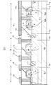
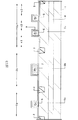
図1は、半導体装置の概略構成を示す模式的断面図である。
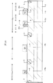
図2は、図1の一部(低耐圧MISFETの部分)を拡大した模式的断面図である。
図3は、図1の一部(高耐圧MISFETの部分)を拡大した模式的断面図である。
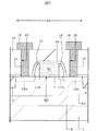
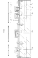
図4は、図1の一部(不揮発性記憶素子の部分)を拡大した模式的断面図である。
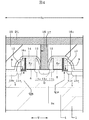
図5は、図4を簡略化して拡大した模式的断面図である。
図6は、図4の不揮発性記憶素子の等価回路図である。
図7乃至図24は、半導体装置の製造工程を示す模式的断面図である。
なお、図12は、図11の一部を拡大した模式的断面図である。
1 to 24 are diagrams relating to a semiconductor device according to an embodiment of the present invention.
FIG. 1 is a schematic cross-sectional view showing a schematic configuration of a semiconductor device.
FIG. 2 is an enlarged schematic cross-sectional view of a part of FIG. 1 (low breakdown voltage MISFET portion).
FIG. 3 is an enlarged schematic cross-sectional view of a part of FIG. 1 (high voltage MISFET part).
FIG. 4 is an enlarged schematic cross-sectional view of a part of FIG. 1 (part of the nonvolatile memory element).
FIG. 5 is a schematic cross-sectional view enlarging and simplifying FIG.
FIG. 6 is an equivalent circuit diagram of the nonvolatile memory element of FIG.
7 to 24 are schematic cross-sectional views showing the manufacturing process of the semiconductor device.
FIG. 12 is an enlarged schematic cross-sectional view of a part of FIG.
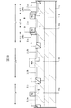
図1に示すように、本実施例の半導体装置は、半導体基板として例えばp型単結晶シリコンからなるシリコン基板1(以下、単に基板1と呼ぶ)を主体に構成されている。
As shown in FIG. 1, the semiconductor device of the present embodiment is mainly composed of a
基板1は、互いに反対側に位置する主面(素子形成面,回路形成面)及び裏面を有し、その主面には、トランジスタ素子の形成領域として使用される活性領域を区画するための素子分離領域3が選択的に形成されている。素子分離領域3は、これに限定されないが、例えば周知のSTI(Shallow Trench Isolation)技術によって形成されている。STI技術による素子分離領域3は、基板1の主面に浅溝(例えば深さが300nm程度の溝)を形成し、その後、前記浅溝の内部を埋め込むようにして基板1の主面上に例えば酸化シリコン膜からなる絶縁膜をCVD(Chemical Vapor Deposition)で形成し、その後、前記浅溝の内部に前記絶縁膜が選択的に残るように前記基板1上の前記絶縁膜をCMP(Chemical Mechanical Polishing:化学的機械研磨)法で除去することによって形成される。素子分離領域3の他の形成方法としては、LOCOS(Locsl Oxidation of Silicon)と呼称される選択酸化法がある。
The
素子分離領域3で区画された活性領域において、活性領域2aには、p型ウエル領域5aが形成されており、このp型ウエル領域5a内にn型低耐圧MISFET−Q1が形成されている。活性領域2bには、p型ウエル領域5bが形成されており、このp型ウエル領域5b内にn型高耐圧MISFET−Q2が形成されている。活性領域2cには、p型ウエル領域5cが形成されており、このp型ウエル領域内に不揮発性記憶素子Qmが形成されている。p型ウエル領域5a〜5cは、基板1の主面に設けられたp型ウエル領域4内に形成されている。
In the active region partitioned by the
基板1の主面上には、活性領域2a〜2cを覆うようにして、例えば酸化シリコン膜からなる層間絶縁膜15が設けられている。基板1の主面と層間絶縁膜15との間には、素子分離領域3、各活性領域(2a〜2c)、並びに各トランジスタを覆うようにして、例えば窒化シリコン膜からなるエッチングストッパ膜14が設けられている。このエッチングストッパ膜14は、層間絶縁膜15をエッチングして接続孔を形成する時のエッチングストッパとして機能する。
On the main surface of the
n型低耐圧MISFET−Q1は、図2に示すように、主に、チャネル形成領域、ゲート絶縁膜6、ゲート電極8a、ソース領域及びドレイン領域を有する構成になっている。ゲート絶縁膜6は、基板1の主面上に設けられている。ゲート電極8aは、基板1の主面上にゲート絶縁膜6を介在して設けられている。チャネル形成領域は、ゲート電極8aの直下における基板1の表層部に設けられている。ソース領域及びドレイン領域は、チャネル形成領域のチャネル長(ゲート長)方向において、チャネル形成領域を挟むようにして基板1の表層部に設けられている。
As shown in FIG. 2, the n-type low breakdown voltage MISFET-Q1 mainly has a channel formation region, a
n型低電圧MISFET−Q1のソース領域及びドレイン領域は、エクステンション領域である一対のn型半導体領域11aと、コンタクト領域である一対のn型半導体領域13aとで構成されている。一対のn型半導体領域11aは、ゲート電極8aに整合して基板1の主面に形成されている。一対のn型半導体領域13aは、ゲート電極8aの側壁に設けられたサイドウォールスペーサ12に整合して基板1の主面に形成されている。
The source region and drain region of the n-type low voltage MISFET-Q1 are composed of a pair of n-
エクステンション領域であるn型半導体領域11aは、コンタクト領域であるn型半導体領域13aよりも高不純物濃度になっている。即ち、本実施例のn型低耐圧MISFET−Q1は、ドレイン領域のチャネル形成領域側の不純物を低濃度化したLDD(Lightly Doped Drain)構造になっている。LDD構造は、ドレイン領域のチャネル形成領域側への拡散量を低減し、チャネル長寸法を確保できるため、短チャネル効果の発生を抑制することができる。また、ドレイン領域とチャネル形成領域との間に形成されるpn接合部の不純物濃度分布の勾配を緩和し、この領域に発生する電界強度を弱められるため、ホットキャリアの発生量を低減することができる。
The n-
各々のn型半導体領域13a上には、層間絶縁膜15の表面からn型半導体領域13aに到達する接続孔16が設けられ、この接続孔16の内部には導電性プラグ17が埋め込まれている。各々のn型半導体領域13aは、導電性プラグ17を介在して、層間絶縁膜15上を延在する配線18と電気的に接続されている。
A
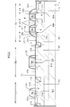
n型高耐圧MISFET−Q2は、図3に示すように、主に、チャネル形成領域、ゲート絶縁膜7、ゲート電極8b、ソース領域及びドレイン領域を有する構成になっている。ゲート絶縁膜7は、基板1の主面上に設けられている。ゲート電極8bは、基板1の主面上にゲート絶縁膜7を介在して設けられている。チャネル形成領域は、ゲート電極8bの直下における基板1の表層部に設けられている。ソース領域及びドレイン領域は、チャネル形成領域のチャネル長(ゲート長)方向において、チャネル形成領域を挟むようにして基板1の表層部に設けられている。
As shown in FIG. 3, the n-type high breakdown voltage MISFET-Q2 mainly has a channel forming region, a
n型高電圧MISFET−Q2のソース領域及びドレイン領域は、エクステンション領域である一対のn型半導体領域11bと、コンタクト領域である一対のn型半導体領域13bとで構成されている。一対のn型半導体領域11bは、ゲート電極8bに整合して基板1の主面に形成されている。一対のn型半導体領域13bは、ゲート電極8bの側壁に設けられたサイドウォールスペーサ12に整合して基板1の主面に形成されている。
The source region and the drain region of the n-type high voltage MISFET-Q2 are composed of a pair of n-
エクステンション領域であるn型半導体領域11bは、コンタクト領域であるn型半導体領域13bよりも高不純物濃度になっている。即ち、本実施例のn型高耐圧MISFET−Q2は、LDD構造になっている。
The n-
n型低耐圧MISFET−Q1及びn型高耐圧MISFET−Q2において、各々のゲート絶縁膜(6,7)は、例えば酸化シリコン膜で形成され、各々のゲート電極(8a,8b)は、例えば抵抗値を低減する不純物が導入された多結晶シリコン膜で形成されている。 In the n-type low breakdown voltage MISFET-Q1 and the n-type high breakdown voltage MISFET-Q2, each gate insulating film (6, 7) is formed of, for example, a silicon oxide film, and each gate electrode (8a, 8b) is formed of, for example, a resistor. It is formed of a polycrystalline silicon film into which an impurity for reducing the value is introduced.
n型高耐圧MISFET−Q2は、高耐圧化を図るため、ゲート絶縁膜7がn型低耐圧MISFET−Q1のゲート絶縁膜6よりも厚い膜厚(7>6)で形成され、更にチャネル長(CL2)がn型低耐圧MISFET−Q1のチャネル長(CL1)よりも長く(CL2>CL1)なっている。
In the n-type high breakdown voltage MISFET-Q2, in order to increase the breakdown voltage, the
各々のn型半導体領域13b上には、層間絶縁膜15の表面からn型半導体領域13bに到達する接続孔16が設けられ、この接続孔16の内部には導電性プラグ17が埋め込まれている。各々のn型半導体領域13bは、導電性プラグ17を介在して、層間絶縁膜15上を延在する配線18と電気的に接続されている。
A
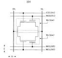
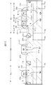
本実施例の半導体装置は、図6に示すメモリセルMcが行列状(同一平面内において直行するX方向及びY方向)に複数配置されたメモリセルアレイを有している。1つのメモリセルMcは、図4に示す1つの不揮発性記憶素子Qmで構成されている。 The semiconductor device of this embodiment has a memory cell array in which a plurality of memory cells Mc shown in FIG. 6 are arranged in a matrix (X direction and Y direction orthogonal to each other in the same plane). One memory cell Mc is composed of one nonvolatile memory element Qm shown in FIG.
不揮発性記憶素子Qmは、図4に示すように、主に、チャネル形成領域、ゲート絶縁膜6、コントロールゲート電極(以下、単にCG電極と呼ぶ)8c、電荷蓄積部として機能するゲート絶縁膜(積層膜)9、メモリゲート電極(以下、単にMG電極と呼ぶ)10c、ソース領域S及びドレイン領域Dを有する構成になっており、等価回路的に制御用FET(パストランジスタ)とMONOS型FETとを直列接続した構成になっている。
As shown in FIG. 4, the nonvolatile memory element Qm mainly includes a channel formation region, a
CG電極8cは、例えば酸化シリコン膜からなるゲート絶縁膜6を介在して基板1の主面上に設けられている。ゲート絶縁膜9は、CG電極8cのチャネル長方向において互いに反対側に位置する2つの側壁面のうちの一方の側壁面側に、この一方の側壁面及び基板1の主面に沿って設けられている。MG電極10cは、基板1及びCG電極8cとの間にゲート絶縁膜9を介在して、CG電極8cの隣り、具体的にはCG電極8cの一方の側壁面側に設けられている。このCG電極8c及びMG電極10cは、これらのゲート長方向に沿って配置されている。
The
CG電極8cの他方の側壁面側(MG電極10cが設けられた側壁面と反対側の側壁面側)には、このCG電極8cと整合して形成されたサイドウォールスペーサ12が設けられている。MG電極10cの外側には、このMG電極10cに整合して形成されたサイドウォールスペーサ12が設けられている。これらのサイドウォールスペーサ12は、例えば酸化シリコン膜からなる絶縁膜で形成されている。
On the other side wall surface side of the
ソース領域S及びドレイン領域Dは、エクステンション領域である一対のn型半導体領域11cと、コンタクト領域である一対のn型半導体領域13cとで構成されている。一対のn型半導体領域11cのうち、一方のn型半導体領域11cは、MG電極10cに整合して基板1の主面に設けられ、他方のn型半導体領域11cは、CG電極8cに整合して基板1の主面に設けられている。一対のn型半導体領域13cのうち、一方のn型半導体領域13cは、MG電極10c側のサイドウォールスペーサ12に整合して基板1の主面に設けられ、他方のn型半導体領域13cは、CG電極8c側のサイドウォールスペーサ12に整合して基板1の主面に設けられている。
The source region S and the drain region D are composed of a pair of n-
エクステンション領域であるn型半導体領域11cは、コンタクト領域であるn型半導体領域13cよりも高不純物濃度になっている。即ち、本実施例の不揮発性記憶素子Qmは、LDD構造になっている。
The n-
チャネル形成領域は、CG電極8c及びMG電極10cの直下、換言すればソース領域Sとドレイン領域Dとの間における基板1の表層部に設けられている。
The channel formation region is provided immediately below the
ゲート絶縁膜9は、例えばONO(酸化膜/窒化膜/酸化膜:Oxide/Nitride/Oxide)の積層膜(多層膜)からなり、本実施例では、図5に示すように、例えば基板1の主面側から酸化シリコン膜(SiO)9a/窒化シリコン膜(SiN)9b/酸化シリコン膜(SiO)9cの順に積層されたONO構造の積層膜で形成されている。
The
図4に示すように、不揮発性記憶素子Qmのドレイン領域であるn型半導体領域13c上には、層間絶縁膜15の表面からn型半導体領域13cに到達する接続孔16が設けられ、この接続孔16の内部には導電性プラグ17が埋め込まれている。n型半導体領域13cは、導電性プラグ17を介在して、層間絶縁膜15上をY方向に沿って延在するデータ線LDと電気的に接続されている。
As shown in FIG. 4, a
不揮発性記憶素子Qmは、メモリセルアレイの平面内において直行するX方向及びY方向に沿って夫々複数配置されている。Y方向において隣り合う不揮発性記憶素子Qmは、ドレイン領域Dであるn型半導体領域13c及びソース領域Sであるn型半導体領域13cが兼用されている。ソース領域であるn型半導体領域13cは、詳細に図示していないがX方向に沿って延在しており、図6に示すソース線SLと電気的に接続されている。ソース配線SLは、図4に図示していないが、データ線DLと同様に、層間絶縁膜15上をY方向に沿って延在している。データ線DL及びソース線SLは、例えばアルミニウム(Al)、又はAl合金、又は銅(Cu)、又はCu合金等の金属膜で形成されている。
A plurality of nonvolatile memory elements Qm are arranged along the X direction and the Y direction perpendicular to each other in the plane of the memory cell array. The nonvolatile memory elements Qm adjacent in the Y direction share the n-
X方向において隣り合う不揮発性記憶素子Qmは、各々のMG電極10cがX方向に沿って延在するゲート線MGL(図6参照)の一部で形成、換言すればゲート線MGLと一体に形成されている。また、X方向において隣り合う不揮発性記憶素子Qmは、各々のCG電極8cがX方向に沿って延在するゲート線CGLの一部で形成、換言すればゲート線CGLと一体に形成されている。ゲート配線MGL及びCGLは、例えば抵抗値を低減する不純物が導入された多結晶シリコン膜で形成されている。
The nonvolatile memory elements Qm adjacent in the X direction are formed by a part of the gate line MGL (see FIG. 6) in which each
不揮発性記憶素子Qmは、等価回路的に制御用FETとMONOS型FETとを直列接続した構成になっており、MG電極10cと基板1との間のゲート絶縁膜9における電荷蓄積膜(本実施例では窒化シリコン膜9b)中のトラップにホットエレクトロン(HE)が注入されると、MONOS型FETの閾値電圧(MG電極10cにおける閾値電圧:Vth)が変化し、制御用FETとMOMOS型FETが直列接続された系全体の閾値電圧(CG電極8cにおける閾値電圧とMG電極10cにおける閾値電圧の系全体の閾値電圧)が変化する。即ち、不揮発性記憶素子Qmは、ゲート絶縁膜9に電荷が蓄積されることで、ソース・ドレイン間に流れるドレイン電流の閾値電圧を制御してメモリ動作する構造になっている。
The nonvolatile memory element Qm has a configuration in which a control FET and a MONOS type FET are connected in series in an equivalent circuit, and a charge storage film in the
なお、ホットエレクトロンが注入される電荷蓄積膜としては、特に窒化シリコン(SiN)膜9bに限るものではなく、例えば酸窒化シリコン(SiON)膜のような膜中に窒素を含有する絶縁膜を用いることもできる。このような酸窒化シリコン膜を用いた場合、窒化シリコン膜に比べてゲート絶縁膜9の耐圧を高めることができる。この結果、後述するようにホットエレクトロン又はホットホールの注入回数に応じたMG電極10c下の基板表面(基板1とゲート絶縁膜9との界面近傍)におけるキャリア移動度の劣化に対する耐性を高めることができる。
The charge storage film into which hot electrons are injected is not limited to the silicon nitride (SiN)
不揮発性記憶素子Qmのデータ書き込みは、例えば、ドレイン領域Dに1V、ソース領域Sに6V、MG電極10cに12V、CG電極8cに1.5V、p型ウエル領域5cに0Vの電圧を夫々印加し、MG電極10c下のチャネル形成領域側(基板1側)からゲート絶縁膜9の窒化シリコン膜9b中にホットエレクトロンを注入することによって行われる。ホットエレクトロンの注入は、ゲート絶縁膜9の下層の酸化シリコン膜9aを通過(トンネリング)させることによって行われる。
For the data writing of the nonvolatile memory element Qm, for example, 1V is applied to the drain region D, 6V to the source region S, 12V to the
不揮発性記憶素子Qmのデータ消去は、例えば、ドレイン領域Dに0V、ソース領域に7V、MG電極10cに−6V、CG電極8c及びp型ウエル領域5cに0Vの電圧を夫々印加し、MG電極10c下のチャネル形成領域側(基板1側)からゲート絶縁膜9の窒化シリコン膜9b中にホットホールを注入することによって行われる。ホットホールの注入は、ゲート絶縁膜9の下層の酸化シリコン膜9aを通過(トンネリング)させることによって行われる。
For example, data erasure of the nonvolatile memory element Qm is performed by applying a voltage of 0 V to the drain region D, 7 V to the source region, −6 V to the
不揮発性記憶素子Qmのデータ読み出しは、例えば、ソース領域Sに0V、ドレイン領域Dに1.5V、MG電極10c及びCG電極8cに1.5V、p型ウエル領域5cに0Vの電圧を夫々印加することによって行われる。
For example, data is read from the nonvolatile memory element Qm by applying a voltage of 0 V to the source region S, 1.5 V to the drain region D, 1.5 V to the
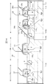
図5に示すように、基板1の主面の活性領域2cには、第1乃至第6の面(1x1〜1x6)が形成されている。この第1乃至第6の面は、基板1の深さ方向における高さ位置(深さ位置)が異なっている。不揮発性記憶素子QmのCG電極8cは、ゲート絶縁膜6を介在して第1の面1x1上に設けられている。
As shown in FIG. 5, first to sixth surfaces (1 × 1 to 1 × 6) are formed in the
第2の面1x2は、第1の面1x1から基板1の深さ方向(基板1の裏面側)に向かって第1の面1x1よりも低い位置(深い位置)に形成されている。この第2の面1x2は、CG電極8cの一方の側壁面側(ソース領域S側)において、CG電極8cに整合して形成されている。不揮発性記憶素子QmのMG電極10cは、CG電極8cと隣り合って第2の面1x2上にゲート絶縁膜9を介在して設けられている。
The second surface 1x2 is formed at a position (deep position) lower than the first surface 1x1 from the first surface 1x1 toward the depth direction of the substrate 1 (the back surface side of the substrate 1). The second surface 1x2 is formed in alignment with the
第3の面1x3は、CG電極8cの他方の側壁面側(ドレインD領域側)において、CG電極8cに整合して形成されている。第4の面1x4は、MG電極10cの外側(ソース領域S側)において、MG電極10cに整合して形成されている。第5の面1x5は、CG電極8cの他方の側壁面側(ドレイン領域D側)に設けられたサイドウォールスペーサ12に整合して形成されている。第6の面1x6は、MG電極10cの外側(ソース領域S側)に設けられたサイドウォールスペーサ12に整合して形成されている。
The third surface 1x3 is formed in alignment with the
第3及び第5の面(1x3,1x5)は、基板1の深さ方向(基板1の裏面側)に向かって第1の面1x1よりも低い位置に形成されており、第5の面1x5は、基板1の深さ方向(基板1の裏面側)に向かって第3の面1x3よりも低い位置に形成されている。第2の面1x2は、基板1の深さ方向(基板1の裏面側)に向かって第3及び第5の面(1x3,1x5)よりも低い位置に形成されている。 The third and fifth surfaces (1x3, 1x5) are formed at positions lower than the first surface 1x1 in the depth direction of the substrate 1 (the back surface side of the substrate 1), and the fifth surface 1x5 Is formed at a position lower than the third surface 1x3 in the depth direction of the substrate 1 (the back surface side of the substrate 1). The second surface 1x2 is formed at a position lower than the third and fifth surfaces (1x3, 1x5) in the depth direction of the substrate 1 (the back surface side of the substrate 1).
第4及び第6の面(1x4,1x6)は、基板1の深さ方向(基板1の裏面側)に向かって第2の面1x1よりも低い位置に形成されており、第6の面1x6は、基板1の深さ方向(基板1の裏面側)に向かって第4の面1x4よりも低い位置に形成されている。 The fourth and sixth surfaces (1x4, 1x6) are formed at positions lower than the second surface 1x1 in the depth direction of the substrate 1 (the back surface side of the substrate 1), and the sixth surface 1x6 Is formed at a position lower than the fourth surface 1x4 in the depth direction of the substrate 1 (the back surface side of the substrate 1).
不揮発性記憶素子Qmのドレイン領域Dにおいて、n型半導体領域11cは、第1の面1x1及び第3の面1x3に亘って設けられており、n型半導体領域13cは、第3の面1x3及び第5の面1x5に亘って設けられている。
In the drain region D of the nonvolatile memory element Qm, the n-
不揮発性記憶素子Qmのソース領域Sにおいて、n型半導体領域11cは、第2の面1x2及び第4の面1x4に亘って設けられており、n型半導体領域13cは、第4の面1x4及び第6の面1x6に亘って設けられている。
In the source region S of the nonvolatile memory element Qm, the n-
第2の面1x2は、後で詳細に説明するが、CG電極8cを形成した後、CG電極8cの一方の側壁面側(ソース領域形成側)の基板表面を選択的にエッチングすることによって形成される。一方、第3乃至第6の面は、n型半導体領域の形成時に使用される犠牲酸化膜(バッファ絶縁膜)を除去することによって形成される。
As will be described in detail later, the second surface 1x2 is formed by selectively etching the substrate surface on one side wall surface side (source region forming side) of the
不揮発性記憶素子Qmのゲート絶縁膜9は、第1の面1x1と第2の面1x2との段差部における壁面を覆うようにして、第2の面1x2からCG電極8cの一方の側壁面に亘って連続的に形成されている。CG電極8cとMG電極10cは、これらの間に介在されたゲート絶縁膜9によって電気的に分離されている。
The
ゲート絶縁膜9の下層の酸化シリコン膜9aとゲート絶縁膜6は、同種の膜であっても成膜工程が異なる膜で形成されており、両者の膜厚が夫々異なっている(9a≠6)。本実施例では、酸化シリコン膜9aは例えば4〜6[nm]程度の膜厚で形成され、ゲート絶縁膜6は例えば2〜3[nm]程度の膜厚の酸化シリコン膜で形成されている(9a>6)。
Even if the
次に、本実施例の半導体装置の製造について、図7乃至図24を用いて説明する。
まず、例えば比抵抗が10[Ωcm]程度のp型単結晶シリコンからなるシリコン基板(基板1)を準備し、その後、基板1の主面に、活性領域(2a,2b,2c)を区画するための素子分離領域3を形成する(図7参照)。素子分離領域3は、例えば周知のSTI技術で形成する。STI技術による素子分離領域3は、まず、基板1の主面に浅溝(例えば深さが300nm程度の溝)を形成し、その後、前記浅溝の内部を埋め込むようにして基板1の主面上に例えば酸化シリコン膜からなる絶縁膜をCVD法で形成し、その後、前記浅溝の内部に前記絶縁膜が選択的に残るように基板1上の前記絶縁膜をCMP法で除去することによって形成される。
Next, the manufacture of the semiconductor device of this example will be described with reference to FIGS.
First, for example, a silicon substrate (substrate 1) made of p-type single crystal silicon having a specific resistance of about 10 [Ωcm] is prepared, and then active regions (2a, 2b, 2c) are partitioned on the main surface of the
次に、図7に示すように、基板1の主面にp型ウエル領域4を形成すると共に、活性領域2aにp型ウエル領域5a、活性領域2bにp型ウエル領域5b、活性領域2cにp型ウエル領域5cを夫々選択的に形成する。これらのウエル領域は、基板1の主面に不純物をイオン注入することによって形成される。
Next, as shown in FIG. 7, a p-
次に、基板1の主面において、図8に示すように、活性領域2a及び2c上に膜厚が薄いゲート絶縁膜6、活性領域2b上にゲート絶縁膜6よりも膜厚が厚いゲート絶縁膜7を選択的に形成する。これらのゲート絶縁膜は、これに限定されないが、例えば、熱酸化処理を施して活性領域2a〜2c上に膜厚が厚い第1の酸化シリコン膜を成膜し、その後、活性領域2a及び2c上の第1の酸化シリコン膜を選択的に除去し、その後、熱酸化処理を施して活性領域2a及び2c上に膜厚が薄い第2の酸化シリコン膜を成膜することによって形成される。
Next, on the main surface of the
ここで、第1及び第2の酸化シリコン膜は、活性領域のシリコン面(半導体面)を酸化することによって形成されるため、この酸化シリコン膜の形成により、活性領域におけるシリコン面の位置は、基板1の深さ方向に若干低くなる。図5に示す第1の面(シリコン面)1x1は、主に、このゲート絶縁膜形成工程において形成される。
Here, since the first and second silicon oxide films are formed by oxidizing the silicon surface (semiconductor surface) of the active region, the position of the silicon surface in the active region is determined by the formation of the silicon oxide film. It becomes slightly lower in the depth direction of the
次に、図9に示すように、ゲート絶縁膜(6,7)を覆うようにして基板1の主面上の全面に、ゲート材として例えば250[nm]程度の膜厚のポリシリコン膜8をCVD法で成膜する。その後、ポリシリコン膜に抵抗値を低減する不純物(例えば砒素(As))をイオン注入する。その後、ポリシリコン膜に注入された不純物を活性化させるための熱処理を施す。
Next, as shown in FIG. 9, a
次に、ポリシリコン膜8をエッチングによりパターンニングして、図10に示すように、活性領域2aのゲート絶縁膜6上にゲート電極8a、活性領域2bのゲート絶縁膜7上にゲート電極8b、活性領域2cのゲート絶縁膜6上にCG電極8cを夫々形成する。
Next, the
ここで、活性領域2cは、CG電極8cを境にして2つの領域に分けられる。この2つの領域のうち、CG電極8cの一方の側壁面側(ソース領域形成側)を第1の領域c1と呼び、CG電極8cの他方の側壁面側(ドレイン領域形成側)を第2の領域c2と呼ぶ。
Here, the
次に、図11に示すように、フォトリソグラフィ技術を用いて基板1の主面上にマスクM1を形成する。マスクM1は、活性領域2a及び2b上、並びに活性領域2cの第2の領域c2上を覆うパターンからなり、かつ活性領域2cの第1の領域c1上に開口部maを有するパターンからなる。
Next, as shown in FIG. 11, a mask M1 is formed on the main surface of the
次に、基板1の主面上にマスクM1が形成された状態で、活性領域2cの第1の領域c1における基板1をエッチングして、図11及び図12に示すように、活性領域2cの第1の領域c1に、基板1の深さ方向に向かって第1の面1x1よりも低い第2の面1x2を形成する。第2の面1x2は、CG電極8cに整合して形成される。基板1のエッチングは、CG電極8c下のゲート絶縁膜6にダメージを与えないために、等方性エッチング(ドライエッチング)で行う。
Next, in a state where the mask M1 is formed on the main surface of the
次に、図13に示すように、第2の面1x2上を含む基板1の主面上の全面に、ONO構造の積層膜(多層膜)からなるゲート絶縁膜9を形成する。ゲート絶縁膜9の形成は、これに限定されないが、例えば、以下のようにして行う。まず、窒素で希釈した酸素雰囲気中で基板1に熱処理を施して、例えば5[nm]程度の膜厚の酸化シリコン膜9aを成膜する。その後、酸化シリコン膜9a上に、電荷蓄積膜として例えば10[nm]程度の膜厚の窒化シリコン膜9bをCVD法で成膜する。その後、窒化シリコン膜9b上に、例えば5[nm]程度の膜厚の酸化シリコン膜9cをCVD法で成膜する。その後、緻密化のための熱処理を施す。これにより、ONO構造の積層膜からなるゲート絶縁膜9が形成される。
Next, as shown in FIG. 13, a
この工程において、電荷蓄積部として機能するゲート絶縁膜9は、第1の面1x1と第2の面1x2との段差部における壁面を覆うようにして、第2の面1x2からCG電極8cの側壁面に亘って連続的に形成される。また、ゲート絶縁膜9の下層の酸化シリコン膜9aは、CG電極8c下のゲート絶縁膜6とは異なる工程で形成される。
In this step, the
なお、電荷蓄積膜としては、窒化シリコン膜9bに代えて、酸化膜の一部に窒素を含有するような絶縁膜、例えば酸窒化シリコン膜を用いることもできる。酸窒化シリコン膜は、例えば、モノシラン(SiH4)等のようなシラン系ガスと、亜酸化窒素(N2O)と、ヘリウム(He)等のような希釈ガスとの混合ガスを用いたCVD法によって形成することができる。
As the charge storage film, an insulating film containing nitrogen in part of the oxide film, for example, a silicon oxynitride film can be used instead of the
次に、図14に示すように、CG電極8cを覆うようにしてゲート絶縁膜9上の全面に、ゲート材として例えば65[nm]程度の膜厚のポリシリコン膜10をCVD法で成膜する。その後、ポリシリコン膜10に抵抗値を低減する不純物をイオン注入し、続いて、ポリシリコン膜10に注入された不純物を活性化させる熱処理を施す。ここで、予め不純物が導入されたポリシリコン膜をCVD法によって成膜することもできる。この場合は、不純物をイオン注入する工程を省略することができる。
Next, as shown in FIG. 14, a
次に、ポリシリコン膜10にRIE(Reactive Ion Eching)等の異方性エッチングを施して、図15に示すように、活性領域2cの第1の領域c1側にサイドウォール形状のMG電極10cを形成する。MG電極10cは、第2の面1x2上及びCG電極8cの隣りに、夫々ゲート絶縁膜9を介在して配置される。また、MG電極10cは、CG電極8cの側壁面を覆うゲート絶縁膜に整合して形成される。
Next, the
この工程において、活性領域2a及び2b、並びに活性領域2cの第2の領域c2側にもMG電極10cと同様のサイドウォール形状の導電体が形成される。
In this step, a sidewall-shaped conductor similar to the
次に、活性領域2cの第1の領域c1側のMG電極10cを残して、活性領域2a及び2b、並びに活性領域2cの第2の領域c2側の前記導電体を選択的に除去し、その後、図16に示すように、CG電極8c及び基板1とMG電極10cとの間に位置するゲート絶縁膜9を除いて他の部分に位置するゲート絶縁膜9を選択的に除去する。
Next, the
次に、エクステンション領域である半導体領域を形成するが、その前に、熱酸化処理を施して、図17に示すように、酸化シリコン膜からなる犠牲酸化膜(バッファ絶縁膜)20を形成する。 Next, a semiconductor region which is an extension region is formed. Before that, a thermal oxidation process is performed to form a sacrificial oxide film (buffer insulating film) 20 made of a silicon oxide film as shown in FIG.
次に、基板1の主面側からその主面の各活性領域(2a,2b,2c)に不純物(例えばAs)を選択的にイオン注入して、図18に示すように、活性領域2aに一対のn型半導体領域11a、活性領域2bに一対のn型半導体領域11b活性領域2cに一対のn型半導体領域11cを形成する。一対のn型半導体領域11aはゲート電極8aに整合して形成され、一対のn型半導体領域11bはゲート電極8bに整合して形成される。また、一対のn型半導体領域11cのうち、一方のn型半導体領域11c(ソース領域)はMG電極10cに整合して形成され、他方のn型半導体領域11c(ドレイン領域)はCG電極8cに整合して形成される。
Next, an impurity (for example, As) is selectively ion-implanted from the main surface side of the
次に、図19に示すように、前述の不純物イオン注入工程で使用した犠牲酸化膜20を除去する。犠牲酸化膜20の除去は、例えばAPM洗浄やHPM洗浄によるウエットエッチングよって行われる。APM洗浄では、主としてアンモニア(NH3またはNH4OH)と過酸化水素(H2O2)と水(H2O)との混合液が洗浄液として用いられる。このAPM洗浄では、主として半導体主面表面の粒子状汚染成分(パーティクル)の除去を目的としている。HPM洗浄では、主として塩酸(HCl)と過酸化水素(H2O2)と水(H2O)との混合液が洗浄液として用いられる。このHPM洗浄では、主として金属汚染成分を除去することを目的としている。
Next, as shown in FIG. 19, the
ここで、犠牲酸化膜20は、活性領域のシリコン面を酸化することによって形成され、洗浄によるウエットエッチングによって除去されるため、この犠牲酸化膜20の形成及び除去により、活性領域におけるシリコン面の位置は、基板1の深さ方向に若干低くなる。図5に示す第3の面1x3及び第4の面1x4は、主に、この犠牲酸化膜20の形成及び除去によって形成される。また、第3の面3x3は、CG電極8cに整合して形成され、第4の面1x4は、MG電極10cに整合して形成される。
Here, since the
次に、図20に示すように、ゲート電極8a及び8bの各々の側壁面にサイドウォールスペーサ12を形成すると共に、CG電極8cの他方の側壁面(第2の領域c2側の側壁面:ドレイン領域形成側の側壁面)、及びMG電極10cの外側(第1の領域c1側:ソース領域形成側)にサイドウォールスペーサ12を形成する。サイドウォールスペーサ12は、基板1の主面上の全面に例えば酸化シリコン膜からなる絶縁膜をCVD法で成膜し、その後、前記絶縁膜にRIE等の異方性エッチングを施すことによって形成される。ゲート電極8a及び8bにおけるサイドウォールスペーサ12は、各々のゲート電極に整合して形成される。CG電極8c側のサイドウォールスペーサ12は、CG電極8cに整合して形成される。MG電極10c側のサイドウォールスペーサ12は、MG電極10cに整合して形成される。
Next, as shown in FIG. 20,
次に、コンタクト領域である半導体領域を形成するが、その前に前述の犠牲酸化膜形成と同様に、熱酸化処理を施して、図21に示すように、酸化シリコン膜からなる犠牲酸化膜(バッファ絶縁膜)21を形成する。 Next, a semiconductor region which is a contact region is formed. Before that, a thermal oxidation process is performed in the same manner as the above-described sacrificial oxide film formation, and a sacrificial oxide film made of a silicon oxide film (see FIG. 21). Buffer insulating film) 21 is formed.
次に、基板1の主面側からその主面の各活性領域(2a,2b,2c)に不純物(例えばAs)を選択的にイオン注入して、図22に示すように、活性領域2aに一対のn型半導体領域13a、活性領域2bに一対のn型半導体領域13b活性領域2cに一対のn型半導体領域13cを形成する。一対のn型半導体領域13aはゲート電極8aの側壁面に設けられたサイドウォールスペーサ12に整合して形成され、一対のn型半導体領域11bはゲート電極8bの側壁面に設けられたサイドウォールスペーサ12に整合して形成される。また、一対のn型半導体領域13cのうち、一方のn型半導体領域13cはMG電極10c側のサイドウォールスペーサ12に整合して形成され、他方のn型半導体領域11cはCG電極8c側のサイドウォールスペーサ12に整合して形成される。この工程により、低耐圧MISFET−Q1、高耐圧MISFET−Q2、不揮発性記憶素子Qmがほぼ完成する。
Next, an impurity (for example, As) is selectively ion-implanted from the main surface side of the
次に、図23に示すように、前述の不純物イオン注入工程で使用した犠牲酸化膜21を除去する。犠牲酸化膜21の除去は、前述の犠牲酸化膜20と同様に、例えばAPM洗浄やHPM洗浄によるウエットエッチングよって行われる。
Next, as shown in FIG. 23, the
ここで、犠牲酸化膜21は、活性領域のシリコン面を酸化することによって形成され、洗浄によるウエットエッチングによって除去されるため、この犠牲酸化膜21の形成及び除去により、活性領域におけるシリコン面の位置は、基板1の深さ方向に若干低くなる。図5に示す第5の面1x5及び第6の面1x6は、主に、この犠牲酸化膜21の形成及び除去によって形成される。また、第5の面1x5は、CG電極8c側のサイドウォールスペーサ12に整合して形成され、第6の面1x6は、MG電極10c側のサイドウォールスペーサ12に整合して形成される。
Here, since the
次に、図24に示すように、各トランジスタ素子のゲート電極を覆うようにして、基板1の主面上の全面に、例えば窒化シリコン膜からなるエッチングストッパ膜14、例えば酸化シリコン膜からなる層間絶縁膜15をCVD法で順次成膜する。その後、層間絶縁膜15の表面を例えばCMP法で平坦化する。
Next, as shown in FIG. 24, an
次に、層間絶縁膜15及びエッチングストッパ膜14を選択的にエッチングして、各トランジスタ素子の半導体領域上に接続孔16を形成する。その後、接続孔16の内部に金属等の導電物を埋め込んで導電性プラグ17を形成する。その後、層間絶縁膜15上に、配線18、データ線DL及びソース線SL等を形成する。これにより、図1乃至図5に示す構造となる。
Next, the
ところで、不揮発性記憶素子Qmのデータ書き込みは、前述したように、基板1側から、MG電極10c下のゲート絶縁膜9における窒化シリコン膜(電荷蓄積膜)9b中にホットエレクトロンを注入することによって行われる。一方、データ消去は、基板1側から、MG電極10c下のゲート絶縁膜9における窒化シリコン膜9b中にホットホールを注入して窒化シリコン膜9b中の電子を消去(中和)することによって行われる。ホットエレクトロン及びホットホールの注入は、ゲート絶縁膜9の下層の酸化シリコン膜9aをトンネリングさせることによって行われる。図5に示すように、データ書き込み時のホットエレクトロン注入は、主にCG電極8c側のa部で行われ、データ消去時のホットホール注入は、主にソース領域S側のb部で行われる。
By the way, as described above, data is written into the nonvolatile memory element Qm by injecting hot electrons from the
このようなデータの書き込み/消去においては、データ書き込み時のホットエレクトロン注入位置(a部)とデータ消去時のホットホール注入位置(b部)とが離れているため、書き込み時のホットエレクトロンと消去時のホットホールとの分布に差が生じ易い。 In such data writing / erasing, the hot electron injection position ( a part) at the time of data writing and the hot hole injection position ( b part) at the time of data erasing are separated. Differences are likely to occur in the distribution of hot holes.
書き込み時のホットエレクトロンと消去時のホットホールとの分布に差が生じると、窒化シリコン膜9b中の電子消去に、より多くのホットホール注入が必要となり、下層の酸化シリコン膜9が劣化し、その結果、データ保持特性の劣化を引き起こす。また、窒化シリコン膜9b中に電子とホールが蓄積され、その結果、データ書き換え耐性の劣化を引き起こす。
If there is a difference in the distribution of hot electrons at the time of writing and hot holes at the time of erasing, more hot holes need to be injected for erasing electrons in the
このような問題を抑制するには、MG電極10cの幅Wを縮小し、ホットエレクトロン注入位置(a部)とホットホール注入位置(b部)とを近づけることが有効である。
In order to suppress such a problem, it is effective to reduce the width W of the
しかしながら、図25に示す従来の不揮発性記憶素子では、メモリゲート電極105の幅Wを狭くした場合、MONOS型FETのメモリゲート電極105におけるチャネル長も短くなるため、MONOS型FETがCut-off出来なくなり(パンチスルー耐性が低下)、その結果、不揮発性記憶素子のオフリーク電流が増大してしまう。
However, in the conventional nonvolatile memory element shown in FIG. 25, when the width W of the
これに対し、本実施例の不揮発性記憶素子Qmは、図5に示すように、基板1の主面において、第1の面1x1上にゲート絶縁膜6を介在してCG電極8cが設けられ、第1の面1x1から基板1の深さ方向に向かって第1の面1x1よりも低い第2の面1x2上に電荷蓄積部として機能するゲート絶縁膜9を介在してMG電極10cが設けられた構造になっている。
On the other hand, as shown in FIG. 5, the non-volatile memory element Qm of the present embodiment is provided with the
このような構造では、(1)第1の面1x1と第2の面1x2との高低差XLに相当する分、MONOS型FETのMG電極10cにおける実効チャネル長が長くなるため、パンチスルー耐性の低下に起因するオフリーク電流の増大を招くことなく、MG電極10cの幅Wを縮小することができる。
In such a structure, (1) since the effective channel length in the
一方、(2)MG電極10cの幅Wを縮小すると、消去時のホットホール生成位置は、CG電極8c側へ近づく。(3)第1の面1x1に対して第2の面1x2を低くする(基板を掘り込む)と、書き込み電流が分散され、書き込み時のホットエレクトロンの生成位置がソース領域S側へ広がる。(4)第1の面1x1と第2の面1x2との段差部(堀り込んだ基板の角の部分)で、電界集中若しくは急激な電圧効果により、インパクトイオン化が強くなる。(5)上記(3)及び(4)の効果により、書き込み時のホットエレクトロンは、効率良く、かつソース領域S側へ広がって注入される。よって、ホットエレクトロン注入位置(a部)とホットホール注入位置(b部)とが近づくため、書き込み時のホットエレクトロンと消去時のホットホールとの分布をほぼ等しくできる。
On the other hand, (2) when the width W of the
従って、不揮発性記憶素子Qmのオフリーク電流の増大を招くことなく、書き換え耐性及びデータ保持特性の向上を図ることができる。 Therefore, it is possible to improve the rewrite durability and the data retention characteristics without increasing the off-leak current of the nonvolatile memory element Qm.
ここで、不揮発性記憶素子Qmは、チャネル長が長すぎると電流利得(駆動能力)が低下し、逆に短すぎるとパンチスルー耐性に起因するオフリーク電流が増加する。従って、電流利得及びオフリーク電流を考慮してチャネル長を変えないことを前提にすると、第1の面1x1と第2の面1x2との高低差XL(基板の堀り込み量)は、10〜30nmの範囲内であることが望ましい。また、基板1の主面は、前述した犠牲酸化膜(20,21)の形成及び除去によって2〜3nm程度削られる。この点も考慮して、第1の面1x1と第2の面1x2との高低差XL(基板の堀り込み量)は、10〜30nmの範囲内であることが望ましい。本実施例では、高低差XLは例えば20nm程度に設定されている。
Here, if the channel length of the nonvolatile memory element Qm is too long, the current gain (driving capability) decreases, and conversely, if it is too short, the off-leak current due to punch-through resistance increases. Therefore, on the assumption that the channel length is not changed in consideration of the current gain and off-leakage current, the height difference XL (the amount of digging of the substrate) between the first surface 1x1 and the second surface 1x2 is 10 to 10. It is desirable to be within the range of 30 nm. Further, the main surface of the
本実施例の不揮発性記憶素子Qmにおいて、制御用FETにおけるゲート絶縁膜6は、図8に示すゲート絶縁膜形成工程で形成されている。一方、MONOS型FETにおけるゲート絶縁膜9は、図13に示すONO膜形成工程で形成されている。即ち、ゲート絶縁膜6と、ゲート絶縁膜9の下層の酸化シリコン膜9aとは、同種の膜であっても成膜工程が異なる膜で形成されている。従って、書き込み時の電界向上に必要な膜厚でゲート絶縁膜6を形成し、ゲート絶縁膜9の窒化シリコン膜から基板側へのリーク電流抑制に必要な膜厚で下層の酸化シリコン膜9aを形成する、換言すれば、データ保持特性により規定された酸化シリコン膜9aの膜厚以下にゲート絶縁膜6を薄膜化することができるため、不揮発性記憶素子Qmの動作電圧の低電圧化を図ることができる。
In the nonvolatile memory element Qm of this example, the
本実施例の不揮発性記憶素子Qmにおいて、第2の面1x2は、図11及び図12に示す基板エッチング工程で形成されている。この基板エッチング工程では、CG電極8cの端部から垂直に削れるドライエッチング(等方性エッチング)で行っている。ウエットエッチングだと、CG電極8c下のゲート絶縁膜6もサイドエッチングにより削られてしまうため、制御用FETの特性が変化してしまう。従って、ドライエッチングで基板1を削ることにより、CG電極8c下のゲート絶縁膜6にダメージを与えることなく、第1の面1x1よりも低い第2の面1x2を形成することができるため、信頼性の高い不揮発性記憶素子Qmを提供することができる。
In the nonvolatile memory element Qm of this example, the second surface 1x2 is formed by the substrate etching process shown in FIGS. In this substrate etching process, dry etching (isotropic etching) is performed that is vertically cut from the end of the
本実施例の不揮発性記憶素子Qmでは、第1の面1x1よりも低い第2の面1x2を設けることで(基板1を掘り込むことで)、書き込み時のホットエレクトロンと消去時のホットホールとの分布をほぼ等しくしているため、共通ワード線内を分割して消去する必要がなく、また、電源容量を増強する必要もない。 In the nonvolatile memory element Qm of this example, by providing a second surface 1x2 lower than the first surface 1x1 (by digging the substrate 1), hot electrons at the time of writing and hot holes at the time of erasing Therefore, it is not necessary to divide and erase the common word line, and it is not necessary to increase the power supply capacity.
本実施例において、第2の面1x2は、図11及び図12に示すように、CG電極8cに整合して形成される。また、MG電極10cは、図15に示すように、CG電極8cの側壁面におけるゲート絶縁膜9に整合して形成される。このようにして第2の面1x2及びMG電極10cを形成することにより、CG電極8cとMG電極10cとの合わせずれを考慮する必要がないため、不揮発性記憶素子Qmの微細化を図ることができる。
In the present embodiment, the second surface 1x2 is formed in alignment with the
以上、本発明者によってなされた発明を、前記実施例に基づき具体的に説明したが、本発明は、前記実施例に限定されるものではなく、その要旨を逸脱しない範囲において種々変更可能であることは勿論である。 As mentioned above, the invention made by the present inventor has been specifically described based on the above embodiments. However, the present invention is not limited to the above embodiments, and various modifications can be made without departing from the scope of the invention. Of course.
1…p型半導体基板(基板)、2a,2b,2c…活性領域、3…素子分離領域、4,5a,5b,5c…p型ウエル領域、6…ゲート絶縁膜、7…ゲート絶縁膜、8a,8b…ゲート電極、8c…コントロールゲート(CG)電極、9…ゲート絶縁膜(積層膜)、9a…酸化シリコン膜、9b…窒化シリコン膜(電荷蓄積膜)、9c…酸化シリコン膜、10c…メモリゲート(MG)電極、11a,11b,11c…n型半導体領域(エクステンション領域)、12…サイドウォールスペーサ、13a,13b,13c…n型半導体領域(コンタクト領域)、14…エッチングストッパ膜、15…層間絶縁膜、16…接続孔、17…導電性プラグ、18…配線、20,21…犠牲酸化膜(バッファ絶縁膜)、Mc…メモリセル、Q1…低耐圧MISFET、Q2…高耐圧MISFET、Qm…不揮発性記憶素子、DL…データ線、SL…ソース線、CGL…コントロールゲート線、MGL…メモリゲート線。
DESCRIPTION OF
Claims (16)
前記半導体基板は、第1の面と、前記第1の面から深さ方向に向かって前記第1の面よりも低い第2の面とを有し、
前記不揮発性記憶素子は、
前記第1の面上に第1の絶縁膜を介在して設けられたコントロールゲート電極と、
前記第1の絶縁膜とは異なる膜からなる第2の絶縁膜、及び前記第2の絶縁膜上に設けられた電荷蓄積膜を含む積層膜と、
前記コントロールゲート電極と隣り合って前記第2の面上に前記積層膜を介在して設けられたメモリゲート電極と、
前記コントロールゲート電極に整合して前記半導体基板に設けられた第1の半導体領域と、
前記メモリゲート電極に整合して前記半導体基板に設けられた第2の半導体領域と、を有し、
前記第1の半導体領域は、前記コントロールゲート電極に整合して形成され、かつ、前記第1の面及び前記第1の面から深さ方向に向かって前記第1の面よりも低い第3の面に亘って設けられ、
前記第2の半導体領域は、前記メモリゲート電極に整合して形成され、かつ、前記第2の面及び前記第2の面から深さ方向に向かって前記第2の面よりも低い第4の面に亘って設けられ、
前記第2の面は、前記半導体基板の深さ方向に向かって前記第3の面よりも低い位置に形成され、
前記不揮発性記憶素子のデータ書き込みは、前記半導体基板側から前記電荷蓄積膜中にホットエレクトロンを注入させることによって行われ、
前記不揮発性記憶素子のデータ消去は、前記半導体基板側から前記電荷蓄積膜中にホットホールを注入させることによって行われ、
前記ホットエレクトロンは、主に前記コントロールゲート電極に近い前記電荷蓄積膜中に注入され、
前記ホットホールは、主に前記第2半導体領域に近い前記電荷蓄積膜中に注入されることを特徴とする半導体装置。 A semiconductor device having a nonvolatile memory element formed on a semiconductor substrate,
The semiconductor substrate has a first surface and a second surface lower than the first surface in the depth direction from the first surface;
The nonvolatile memory element is
A control gate electrode provided on the first surface with a first insulating film interposed therebetween;
A second insulating film made of a film different from the first insulating film, and a stacked film including a charge storage film provided on the second insulating film;
A memory gate electrode provided adjacent to the control gate electrode on the second surface with the stacked film interposed therebetween;
A first semiconductor region provided in the semiconductor substrate in alignment with the control gate electrode;
Aligned with the memory gate electrode to have a, a second semiconductor region provided in the semiconductor substrate,
The first semiconductor region is formed in alignment with the control gate electrode, and is lower than the first surface in the depth direction from the first surface and the first surface. Provided across the surface,
The second semiconductor region is formed in alignment with the memory gate electrode, and is lower than the second surface in the depth direction from the second surface and the second surface. Provided across the surface,
The second surface is formed at a position lower than the third surface in the depth direction of the semiconductor substrate,
Data writing to the nonvolatile memory element is performed by injecting hot electrons into the charge storage film from the semiconductor substrate side,
Data erasure of the nonvolatile memory element is performed by injecting hot holes into the charge storage film from the semiconductor substrate side,
The hot electrons are mainly injected into the charge storage film close to the control gate electrode,
The hot hole is mainly injected into the charge storage film close to the second semiconductor region .
前記第1及び第2の絶縁膜は、夫々の膜厚が異なっていることを特徴とする半導体装置。 The semiconductor device according to claim 1,
The semiconductor device according to claim 1, wherein the first and second insulating films have different film thicknesses.
前記第2の絶縁膜は、前記第1の絶縁膜よりも膜厚が厚いことを特徴とする半導体装置。 The semiconductor device according to claim 1,
The semiconductor device, wherein the second insulating film is thicker than the first insulating film.
前記第2の絶縁膜は、前記第1の面と前記第2の面との段差部における壁面を覆うようにして、前記第2の面から前記コントロールゲート電極の側面に亘って形成されていることを特徴とする半導体装置。 The semiconductor device according to claim 1,
The second insulating film is formed from the second surface to the side surface of the control gate electrode so as to cover a wall surface at a step portion between the first surface and the second surface. A semiconductor device.
前記積層膜は、前記第1の面と前記第2の面との段差部における壁面を覆うようにして、前記第2の面から前記コントロールゲート電極の側面に亘って形成され、
前記コントロールゲート電極と前記メモリゲート電極は、前記積層膜によって電気的に分離されていることを特徴とする半導体装置。 The semiconductor device according to claim 1,
The laminated film is formed from the second surface to the side surface of the control gate electrode so as to cover a wall surface at a step portion between the first surface and the second surface,
The memory gate electrode and the control Ruge over gate electrode is a semiconductor device characterized by being electrically isolated by the laminated film.
前記第2の面と前記第1の面との高低差は、10〜30[nm]の範囲内であることを特徴とする半導体装置。 The semiconductor device according to claim 1,
A difference in height between the second surface and the first surface is in a range of 10 to 30 [nm].
前記第1の半導体領域はドレイン領域であり、前記第2の半導体領域はソース領域であることを特徴とする半導体装置。 The semiconductor device according to claim 1,
The semiconductor device, wherein the first semiconductor region is a drain region and the second semiconductor region is a source region.
前記第1及び第2の絶縁膜は酸化膜であり、前記電荷蓄積膜は窒化膜であることを特徴とする半導体装置。 The semiconductor device according to claim 1,
The semiconductor device according to claim 1, wherein the first and second insulating films are oxide films, and the charge storage film is a nitride film.
前記積層膜は、前記電荷蓄積膜上に形成された第3の絶縁膜を含み、
前記第1乃至第3の絶縁膜は酸化膜であり、前記電荷蓄積膜は窒化膜であることを特徴とする半導体装置。 The semiconductor device according to claim 1,
The stacked film includes a third insulating film formed on the charge storage film,
The semiconductor device according to claim 1, wherein the first to third insulating films are oxide films, and the charge storage film is a nitride film.
(a)半導体基板の第1の面上に第1の絶縁膜を介在し、一方の側壁面側に第1の領域を有し、かつ、他方の側壁側に第2の領域を有するコントロールゲート電極を形成する工程と、
(b)前記(a)工程の後、前記半導体基板上に、前記コントロールゲート電極の前記第2の領域を覆い、かつ、前記第1の領域上に開口部を有するパターンからなるマスクを形成する工程と、
(c)前記(b)工程の後、前記マスクが形成された状態で、前記半導体基板をエッチングすることにより、前記第1の面から深さ方向に前記第1の面よりも低い第2の面を形成する工程と、
(d)前記(c)工程の後、前記第2の面上に、前記第2の面側から順次積層された第2の絶縁膜及び電荷蓄積膜を含む積層膜を形成する工程と、
(e)前記(d)工程の後、前記第2の面上に前記積層膜を介在してメモリゲート電極を形成する工程と、
(f)前記(e)工程の後、熱酸化処理を施して前記半導体基板に犠牲酸化膜を形成する工程と、
(g)前記(f)工程の後、前記犠牲酸化膜で覆われた前記半導体基板に不純物をイオン注入して、前記コントロールゲート電極に整合した第1の半導体領域と、前記メモリゲート電極に整合した第2の半導体領域とを形成する工程と、
(h)前記(g)工程の後、前記犠牲酸化膜を洗浄にて除去する工程と、を有し、
前記(h)工程における洗浄により前記犠牲酸化膜が除去されることにより、前記第1の面から深さ方向に向かって前記第1の面よりも低い第3の面、及び、前記第2の面から深さ方向に向かって前記第2の面よりも低い第4の面が形成され、
前記第1の半導体領域は、前記第1の面及び前記第3の面に亘って設けられ、
前記第2の半導体領域は、前記第2の面及び前記第4の面に亘って設けられ、
前記第2の面は、前記半導体基板の深さ方向に向かって前記第3の面よりも低い位置に形成され、
前記不揮発性記憶素子のデータ書き込みは、前記半導体基板側から前記電荷蓄積膜中にホットエレクトロンを注入させることによって行われ、
前記不揮発性記憶素子のデータ消去は、前記半導体基板側から前記電荷蓄積膜中にホットホールを注入させることによって行われ、
前記ホットエレクトロンは、主に前記コントロールゲート電極に近い前記電荷蓄積膜中に注入され、
前記ホットホールは、主に前記第2半導体領域に近い前記電荷蓄積膜中に注入されることを特徴とする半導体装置の製造方法。 A method of manufacturing a semiconductor device having a nonvolatile memory element,
(A) A control gate having a first insulating film on a first surface of a semiconductor substrate, a first region on one side wall surface side, and a second region on the other side wall surface Forming an electrode;
(B) After the step (a), a mask made of a pattern that covers the second region of the control gate electrode and has an opening on the first region is formed on the semiconductor substrate. Process,
( C ) After the step ( b ), by etching the semiconductor substrate with the mask formed, a second lower than the first surface in the depth direction from the first surface. Forming a surface;
( D ) after the step ( c ), forming a stacked film including a second insulating film and a charge storage film sequentially stacked from the second surface side on the second surface;
(E) after step (d), and as engineering that form a memory gate electrode by interposing the laminated film on the second surface,
(F) After the step (e), performing a thermal oxidation process to form a sacrificial oxide film on the semiconductor substrate;
(G) After the step (f), impurities are ion-implanted into the semiconductor substrate covered with the sacrificial oxide film, and the first semiconductor region aligned with the control gate electrode is aligned with the memory gate electrode. Forming the second semiconductor region formed;
(H) after step (g), have a, and removing the sacrificial oxide film by washing,
By removing the sacrificial oxide film by the cleaning in the step (h), a third surface lower than the first surface in the depth direction from the first surface, and the second surface A fourth surface lower than the second surface is formed in the depth direction from the surface;
The first semiconductor region is provided across the first surface and the third surface,
The second semiconductor region is provided across the second surface and the fourth surface,
The second surface is formed at a position lower than the third surface in the depth direction of the semiconductor substrate,
Data writing to the nonvolatile memory element is performed by injecting hot electrons into the charge storage film from the semiconductor substrate side,
Data erasure of the nonvolatile memory element is performed by injecting hot holes into the charge storage film from the semiconductor substrate side,
The hot electrons are mainly injected into the charge storage film close to the control gate electrode,
The method for manufacturing a semiconductor device is characterized in that the hot holes are mainly injected into the charge storage film close to the second semiconductor region .
前記第2の面は、前記コントロールゲート電極に整合して形成されることを特徴とする半導体装置の製造方法。 The method of manufacturing a semiconductor device according to claim 1 0,
The method of manufacturing a semiconductor device, wherein the second surface is formed in alignment with the control gate electrode.
前記半導体基板のエッチングは、ドライエッチングであることを特徴とする半導体装置の製造方法。 The method of manufacturing a semiconductor device according to claim 1 0,
The method for manufacturing a semiconductor device, wherein the etching of the semiconductor substrate is dry etching.
前記半導体基板のエッチングは、前記第1の面と前記第2の面との高低差が10〜30[nm]の範囲内になるように行うことを特徴とする半導体装置の製造方法。 The method of manufacturing a semiconductor device according to claim 1 0,
Etching of the semiconductor substrate is performed so that a height difference between the first surface and the second surface is within a range of 10 to 30 [nm].
前記第2の絶縁膜は、前記第1の絶縁膜よりも厚さが厚いことを特徴とする半導体装置の製造方法。 The method of manufacturing a semiconductor device according to claim 1 0,
The method for manufacturing a semiconductor device, wherein the second insulating film is thicker than the first insulating film.
前記積層膜は、前記第1の面と前記第2の面との段差部の壁面を覆うようにして前記第2の面から前記コントロールゲート電極の側面に亘って形成され、
前記メモリゲート電極は、前記コントロールゲート電極の隣に前記積層膜を介在して形成されることを特徴とする半導体装置の製造方法。 The method of manufacturing a semiconductor device according to claim 1 0,
The laminated film is formed from the second surface to the side surface of the control gate electrode so as to cover the wall surface of the step portion between the first surface and the second surface,
The method of manufacturing a semiconductor device, wherein the memory gate electrode is formed adjacent to the control gate electrode with the stacked film interposed therebetween.
前記第1の半導体領域はドレイン領域であり、前記第2の半導体領域はソース領域であることを特徴とする半導体装置の製造方法。 The method of manufacturing a semiconductor device according to claim 1 0,
The method of manufacturing a semiconductor device, wherein the first semiconductor region is a drain region and the second semiconductor region is a source region.
Priority Applications (1)
| Application Number | Priority Date | Filing Date | Title |
|---|---|---|---|
| JP2005150304A JP5014591B2 (en) | 2005-05-24 | 2005-05-24 | Semiconductor device and manufacturing method thereof |
Applications Claiming Priority (1)
| Application Number | Priority Date | Filing Date | Title |
|---|---|---|---|
| JP2005150304A JP5014591B2 (en) | 2005-05-24 | 2005-05-24 | Semiconductor device and manufacturing method thereof |
Publications (2)
| Publication Number | Publication Date |
|---|---|
| JP2006332143A JP2006332143A (en) | 2006-12-07 |
| JP5014591B2 true JP5014591B2 (en) | 2012-08-29 |
Family
ID=37553554
Family Applications (1)
| Application Number | Title | Priority Date | Filing Date |
|---|---|---|---|
| JP2005150304A Expired - Fee Related JP5014591B2 (en) | 2005-05-24 | 2005-05-24 | Semiconductor device and manufacturing method thereof |
Country Status (1)
| Country | Link |
|---|---|
| JP (1) | JP5014591B2 (en) |
Families Citing this family (4)
| Publication number | Priority date | Publication date | Assignee | Title |
|---|---|---|---|---|
| JP6450624B2 (en) * | 2015-03-30 | 2019-01-09 | ルネサスエレクトロニクス株式会社 | Semiconductor device and manufacturing method thereof |
| CN106716637A (en) | 2015-03-30 | 2017-05-24 | 瑞萨电子株式会社 | Semiconductor device and manufacturing method thereof |
| JP6557095B2 (en) * | 2015-08-26 | 2019-08-07 | ルネサスエレクトロニクス株式会社 | Semiconductor device |
| JP6594198B2 (en) | 2015-12-28 | 2019-10-23 | ルネサスエレクトロニクス株式会社 | Semiconductor device and manufacturing method thereof |
Family Cites Families (4)
| Publication number | Priority date | Publication date | Assignee | Title |
|---|---|---|---|---|
| JP4547749B2 (en) * | 1999-09-29 | 2010-09-22 | ソニー株式会社 | Nonvolatile semiconductor memory device |
| JP2003110015A (en) * | 2001-09-28 | 2003-04-11 | Sanyo Electric Co Ltd | Method of fabricating semiconductor device |
| JP4601287B2 (en) * | 2002-12-26 | 2010-12-22 | ルネサスエレクトロニクス株式会社 | Nonvolatile semiconductor memory device |
| JP2004303918A (en) * | 2003-03-31 | 2004-10-28 | Renesas Technology Corp | Semiconductor device manufacturing method and semiconductor device |
-
2005
- 2005-05-24 JP JP2005150304A patent/JP5014591B2/en not_active Expired - Fee Related
Also Published As
| Publication number | Publication date |
|---|---|
| JP2006332143A (en) | 2006-12-07 |
Similar Documents
| Publication | Publication Date | Title |
|---|---|---|
| US8344444B2 (en) | Semiconductor device having a nonvolatile memory cell with a cap insulating film formed over a selection gate electrode | |
| JP5191633B2 (en) | Semiconductor device and manufacturing method thereof | |
| JP5007017B2 (en) | Manufacturing method of semiconductor device | |
| JP4620334B2 (en) | Semiconductor memory device, semiconductor device, portable electronic device including them, and IC card | |
| US10600799B2 (en) | Memory device and low breakdown voltage transistor | |
| US20040245564A1 (en) | Semiconductor storage device, semiconductor device and their manufacturing methods, and portable electronic equipment, and IC card | |
| JP5538828B2 (en) | Semiconductor device and manufacturing method thereof | |
| CN105226064B (en) | Semiconductor device and method of manufacturing the same | |
| US9214350B2 (en) | Semiconductor device having a capacitive element | |
| US7595237B2 (en) | Non-volatile memory cell with a hybrid access transistor | |
| CN109994542B (en) | Semiconductor device and method for manufacturing the same | |
| US10325899B2 (en) | Semiconductor device including transistors formed in regions of semiconductor substrate and operation method of the same | |
| US11342430B2 (en) | Semiconductor device | |
| JP4405489B2 (en) | Nonvolatile semiconductor memory | |
| US7715242B2 (en) | Erasing method of non-volatile memory | |
| TW200816397A (en) | Flash memory device with single-poly structure and method for manufacturing the same | |
| JP2009010281A (en) | Semiconductor device and manufacturing method thereof | |
| JP5014591B2 (en) | Semiconductor device and manufacturing method thereof | |
| US9831093B2 (en) | Semiconductor device and manufacturing method thereof | |
| US11264473B2 (en) | Method for manufacturing semiconductor device | |
| JP5351274B2 (en) | Nonvolatile semiconductor memory device | |
| JP2004342881A (en) | Semiconductor storage device, semiconductor device, IC card, portable electronic device, and method of manufacturing semiconductor storage device | |
| JP2004349304A (en) | Semiconductor storage device, semiconductor device and manufacturing method thereof, portable electronic device, and IC card | |
| JP2010093154A (en) | Nonvolatile semiconductor memory device and method for manufacturing the same |
Legal Events
| Date | Code | Title | Description |
|---|---|---|---|
| A621 | Written request for application examination |
Free format text: JAPANESE INTERMEDIATE CODE: A621 Effective date: 20080409 |
|
| A977 | Report on retrieval |
Free format text: JAPANESE INTERMEDIATE CODE: A971007 Effective date: 20100412 |
|
| A711 | Notification of change in applicant |
Free format text: JAPANESE INTERMEDIATE CODE: A712 Effective date: 20100511 |
|
| A131 | Notification of reasons for refusal |
Free format text: JAPANESE INTERMEDIATE CODE: A131 Effective date: 20111115 |
|
| A521 | Request for written amendment filed |
Free format text: JAPANESE INTERMEDIATE CODE: A523 Effective date: 20120113 |
|
| A131 | Notification of reasons for refusal |
Free format text: JAPANESE INTERMEDIATE CODE: A131 Effective date: 20120306 |
|
| TRDD | Decision of grant or rejection written | ||
| A01 | Written decision to grant a patent or to grant a registration (utility model) |
Free format text: JAPANESE INTERMEDIATE CODE: A01 Effective date: 20120605 |
|
| A01 | Written decision to grant a patent or to grant a registration (utility model) |
Free format text: JAPANESE INTERMEDIATE CODE: A01 |
|
| A61 | First payment of annual fees (during grant procedure) |
Free format text: JAPANESE INTERMEDIATE CODE: A61 Effective date: 20120606 |
|
| FPAY | Renewal fee payment (event date is renewal date of database) |
Free format text: PAYMENT UNTIL: 20150615 Year of fee payment: 3 |
|
| R150 | Certificate of patent or registration of utility model |
Free format text: JAPANESE INTERMEDIATE CODE: R150 |
|
| S531 | Written request for registration of change of domicile |
Free format text: JAPANESE INTERMEDIATE CODE: R313531 |
|
| R350 | Written notification of registration of transfer |
Free format text: JAPANESE INTERMEDIATE CODE: R350 |
|
| LAPS | Cancellation because of no payment of annual fees |