JP2004303918A - Semiconductor device and method of manufacturing the same - Google Patents
Semiconductor device and method of manufacturing the same Download PDFInfo
- Publication number
- JP2004303918A JP2004303918A JP2003094517A JP2003094517A JP2004303918A JP 2004303918 A JP2004303918 A JP 2004303918A JP 2003094517 A JP2003094517 A JP 2003094517A JP 2003094517 A JP2003094517 A JP 2003094517A JP 2004303918 A JP2004303918 A JP 2004303918A
- Authority
- JP
- Japan
- Prior art keywords
- gate electrode
- effect transistor
- field
- memory
- semiconductor device
- Prior art date
- Legal status (The legal status is an assumption and is not a legal conclusion. Google has not performed a legal analysis and makes no representation as to the accuracy of the status listed.)
- Pending
Links
- 239000004065 semiconductor Substances 0.000 title claims abstract description 431
- 238000004519 manufacturing process Methods 0.000 title claims description 117
- 230000015654 memory Effects 0.000 claims abstract description 498
- 239000000758 substrate Substances 0.000 claims abstract description 211
- 238000000034 method Methods 0.000 claims abstract description 98
- 238000005530 etching Methods 0.000 claims abstract description 48
- 238000009825 accumulation Methods 0.000 claims abstract description 5
- 238000003860 storage Methods 0.000 claims description 132
- 230000005669 field effect Effects 0.000 claims description 125
- 239000012535 impurity Substances 0.000 claims description 93
- 239000004020 conductor Substances 0.000 claims description 60
- 230000015572 biosynthetic process Effects 0.000 claims description 49
- 238000013500 data storage Methods 0.000 claims description 28
- 238000000059 patterning Methods 0.000 claims description 21
- 229910052581 Si3N4 Inorganic materials 0.000 claims description 18
- 229910021332 silicide Inorganic materials 0.000 claims description 18
- FVBUAEGBCNSCDD-UHFFFAOYSA-N silicide(4-) Chemical compound [Si-4] FVBUAEGBCNSCDD-UHFFFAOYSA-N 0.000 claims description 18
- HQVNEWCFYHHQES-UHFFFAOYSA-N silicon nitride Chemical compound N12[Si]34N5[Si]62N3[Si]51N64 HQVNEWCFYHHQES-UHFFFAOYSA-N 0.000 claims description 18
- 230000001681 protective effect Effects 0.000 claims description 17
- 238000000151 deposition Methods 0.000 claims description 12
- 230000000694 effects Effects 0.000 claims description 10
- 125000006850 spacer group Chemical group 0.000 claims description 8
- 230000005684 electric field Effects 0.000 claims description 6
- 230000006870 function Effects 0.000 claims description 6
- 230000006798 recombination Effects 0.000 claims description 2
- 238000005215 recombination Methods 0.000 claims description 2
- 230000008569 process Effects 0.000 abstract description 32
- 150000004767 nitrides Chemical class 0.000 abstract description 11
- 229920002120 photoresistant polymer Polymers 0.000 abstract description 4
- 239000010410 layer Substances 0.000 description 155
- VYPSYNLAJGMNEJ-UHFFFAOYSA-N Silicium dioxide Chemical compound O=[Si]=O VYPSYNLAJGMNEJ-UHFFFAOYSA-N 0.000 description 37
- 229910052814 silicon oxide Inorganic materials 0.000 description 37
- 229910021420 polycrystalline silicon Inorganic materials 0.000 description 36
- 229920005591 polysilicon Polymers 0.000 description 32
- 238000005229 chemical vapour deposition Methods 0.000 description 25
- 230000003647 oxidation Effects 0.000 description 16
- 238000007254 oxidation reaction Methods 0.000 description 16
- 229910052751 metal Inorganic materials 0.000 description 15
- 239000002184 metal Substances 0.000 description 15
- 238000001312 dry etching Methods 0.000 description 13
- 229910052785 arsenic Inorganic materials 0.000 description 12
- RQNWIZPPADIBDY-UHFFFAOYSA-N arsenic atom Chemical compound [As] RQNWIZPPADIBDY-UHFFFAOYSA-N 0.000 description 12
- 150000002500 ions Chemical class 0.000 description 12
- OAICVXFJPJFONN-UHFFFAOYSA-N Phosphorus Chemical compound [P] OAICVXFJPJFONN-UHFFFAOYSA-N 0.000 description 11
- OKZIUSOJQLYFSE-UHFFFAOYSA-N difluoroboron Chemical compound F[B]F OKZIUSOJQLYFSE-UHFFFAOYSA-N 0.000 description 11
- 229910052698 phosphorus Inorganic materials 0.000 description 11
- 239000011574 phosphorus Substances 0.000 description 11
- IJGRMHOSHXDMSA-UHFFFAOYSA-N Atomic nitrogen Chemical compound N#N IJGRMHOSHXDMSA-UHFFFAOYSA-N 0.000 description 10
- 230000007423 decrease Effects 0.000 description 10
- 238000002513 implantation Methods 0.000 description 10
- 238000001039 wet etching Methods 0.000 description 10
- 238000005468 ion implantation Methods 0.000 description 9
- 238000001459 lithography Methods 0.000 description 9
- ZOXJGFHDIHLPTG-UHFFFAOYSA-N Boron Chemical compound [B] ZOXJGFHDIHLPTG-UHFFFAOYSA-N 0.000 description 8
- XUIMIQQOPSSXEZ-UHFFFAOYSA-N Silicon Chemical compound [Si] XUIMIQQOPSSXEZ-UHFFFAOYSA-N 0.000 description 8
- 229910052796 boron Inorganic materials 0.000 description 8
- 230000015556 catabolic process Effects 0.000 description 8
- 230000004048 modification Effects 0.000 description 8
- 238000012986 modification Methods 0.000 description 8
- 229910052710 silicon Inorganic materials 0.000 description 8
- 239000010703 silicon Substances 0.000 description 8
- 230000004888 barrier function Effects 0.000 description 7
- 230000007547 defect Effects 0.000 description 7
- 238000010586 diagram Methods 0.000 description 7
- 239000002784 hot electron Substances 0.000 description 7
- 238000002347 injection Methods 0.000 description 7
- 239000007924 injection Substances 0.000 description 7
- 239000000463 material Substances 0.000 description 6
- 230000000630 rising effect Effects 0.000 description 6
- 239000002159 nanocrystal Substances 0.000 description 5
- 229910052757 nitrogen Inorganic materials 0.000 description 5
- 230000005641 tunneling Effects 0.000 description 5
- NBIIXXVUZAFLBC-UHFFFAOYSA-N Phosphoric acid Chemical compound OP(O)(O)=O NBIIXXVUZAFLBC-UHFFFAOYSA-N 0.000 description 4
- 230000002159 abnormal effect Effects 0.000 description 4
- 239000013078 crystal Substances 0.000 description 4
- 238000013461 design Methods 0.000 description 4
- 238000007667 floating Methods 0.000 description 4
- 230000014759 maintenance of location Effects 0.000 description 4
- 230000002093 peripheral effect Effects 0.000 description 4
- 239000010936 titanium Substances 0.000 description 4
- PXHVJJICTQNCMI-UHFFFAOYSA-N Nickel Chemical compound [Ni] PXHVJJICTQNCMI-UHFFFAOYSA-N 0.000 description 3
- 101000900567 Pisum sativum Disease resistance response protein Pi49 Proteins 0.000 description 3
- 238000000137 annealing Methods 0.000 description 3
- 239000000969 carrier Substances 0.000 description 3
- 239000010941 cobalt Substances 0.000 description 3
- 229910017052 cobalt Inorganic materials 0.000 description 3
- GUTLYIVDDKVIGB-UHFFFAOYSA-N cobalt atom Chemical compound [Co] GUTLYIVDDKVIGB-UHFFFAOYSA-N 0.000 description 3
- 238000005516 engineering process Methods 0.000 description 3
- 229910044991 metal oxide Inorganic materials 0.000 description 3
- 238000012545 processing Methods 0.000 description 3
- 238000000926 separation method Methods 0.000 description 3
- WFKWXMTUELFFGS-UHFFFAOYSA-N tungsten Chemical compound [W] WFKWXMTUELFFGS-UHFFFAOYSA-N 0.000 description 3
- 229910052721 tungsten Inorganic materials 0.000 description 3
- 239000010937 tungsten Substances 0.000 description 3
- -1 Metal Oxide Nitride Chemical class 0.000 description 2
- 229910004298 SiO 2 Inorganic materials 0.000 description 2
- BOTDANWDWHJENH-UHFFFAOYSA-N Tetraethyl orthosilicate Chemical compound CCO[Si](OCC)(OCC)OCC BOTDANWDWHJENH-UHFFFAOYSA-N 0.000 description 2
- RTAQQCXQSZGOHL-UHFFFAOYSA-N Titanium Chemical compound [Ti] RTAQQCXQSZGOHL-UHFFFAOYSA-N 0.000 description 2
- 229910052782 aluminium Inorganic materials 0.000 description 2
- XAGFODPZIPBFFR-UHFFFAOYSA-N aluminium Chemical compound [Al] XAGFODPZIPBFFR-UHFFFAOYSA-N 0.000 description 2
- 229910000147 aluminium phosphate Inorganic materials 0.000 description 2
- QVGXLLKOCUKJST-UHFFFAOYSA-N atomic oxygen Chemical compound [O] QVGXLLKOCUKJST-UHFFFAOYSA-N 0.000 description 2
- 239000000470 constituent Substances 0.000 description 2
- 230000006866 deterioration Effects 0.000 description 2
- 238000011161 development Methods 0.000 description 2
- 230000018109 developmental process Effects 0.000 description 2
- 238000000605 extraction Methods 0.000 description 2
- 239000007789 gas Substances 0.000 description 2
- 239000012212 insulator Substances 0.000 description 2
- 230000008018 melting Effects 0.000 description 2
- 238000002844 melting Methods 0.000 description 2
- 239000000203 mixture Substances 0.000 description 2
- 239000001301 oxygen Substances 0.000 description 2
- 229910052760 oxygen Inorganic materials 0.000 description 2
- 238000004904 shortening Methods 0.000 description 2
- 239000002344 surface layer Substances 0.000 description 2
- 229910052719 titanium Inorganic materials 0.000 description 2
- BLRPTPMANUNPDV-UHFFFAOYSA-N Silane Chemical compound [SiH4] BLRPTPMANUNPDV-UHFFFAOYSA-N 0.000 description 1
- NRTOMJZYCJJWKI-UHFFFAOYSA-N Titanium nitride Chemical compound [Ti]#N NRTOMJZYCJJWKI-UHFFFAOYSA-N 0.000 description 1
- IVHJCRXBQPGLOV-UHFFFAOYSA-N azanylidynetungsten Chemical compound [W]#N IVHJCRXBQPGLOV-UHFFFAOYSA-N 0.000 description 1
- 230000006399 behavior Effects 0.000 description 1
- 230000008901 benefit Effects 0.000 description 1
- 238000006243 chemical reaction Methods 0.000 description 1
- 238000004140 cleaning Methods 0.000 description 1
- 238000004891 communication Methods 0.000 description 1
- 238000006731 degradation reaction Methods 0.000 description 1
- 230000003111 delayed effect Effects 0.000 description 1
- 230000000779 depleting effect Effects 0.000 description 1
- 230000008021 deposition Effects 0.000 description 1
- 230000000994 depressogenic effect Effects 0.000 description 1
- 238000011982 device technology Methods 0.000 description 1
- 238000009792 diffusion process Methods 0.000 description 1
- 238000009826 distribution Methods 0.000 description 1
- 230000012447 hatching Effects 0.000 description 1
- 238000010438 heat treatment Methods 0.000 description 1
- 230000010365 information processing Effects 0.000 description 1
- 230000010354 integration Effects 0.000 description 1
- 238000002955 isolation Methods 0.000 description 1
- 150000004706 metal oxides Chemical class 0.000 description 1
- 229910052759 nickel Inorganic materials 0.000 description 1
- 230000001590 oxidative effect Effects 0.000 description 1
- 238000000206 photolithography Methods 0.000 description 1
- 238000009832 plasma treatment Methods 0.000 description 1
- 230000009467 reduction Effects 0.000 description 1
- 239000003870 refractory metal Substances 0.000 description 1
- 239000002356 single layer Substances 0.000 description 1
- 238000004544 sputter deposition Methods 0.000 description 1
- WQJQOUPTWCFRMM-UHFFFAOYSA-N tungsten disilicide Chemical compound [Si]#[W]#[Si] WQJQOUPTWCFRMM-UHFFFAOYSA-N 0.000 description 1
- 229910021342 tungsten silicide Inorganic materials 0.000 description 1
Images


Classifications
-
- B—PERFORMING OPERATIONS; TRANSPORTING
- B23—MACHINE TOOLS; METAL-WORKING NOT OTHERWISE PROVIDED FOR
- B23H—WORKING OF METAL BY THE ACTION OF A HIGH CONCENTRATION OF ELECTRIC CURRENT ON A WORKPIECE USING AN ELECTRODE WHICH TAKES THE PLACE OF A TOOL; SUCH WORKING COMBINED WITH OTHER FORMS OF WORKING OF METAL
- B23H7/00—Processes or apparatus applicable to both electrical discharge machining and electrochemical machining
- B23H7/02—Wire-cutting
-
- H—ELECTRICITY
- H01—ELECTRIC ELEMENTS
- H01L—SEMICONDUCTOR DEVICES NOT COVERED BY CLASS H10
- H01L29/00—Semiconductor devices adapted for rectifying, amplifying, oscillating or switching, or capacitors or resistors with at least one potential-jump barrier or surface barrier, e.g. PN junction depletion layer or carrier concentration layer; Details of semiconductor bodies or of electrodes thereof ; Multistep manufacturing processes therefor
- H01L29/66—Types of semiconductor device ; Multistep manufacturing processes therefor
- H01L29/66007—Multistep manufacturing processes
- H01L29/66075—Multistep manufacturing processes of devices having semiconductor bodies comprising group 14 or group 13/15 materials
- H01L29/66227—Multistep manufacturing processes of devices having semiconductor bodies comprising group 14 or group 13/15 materials the devices being controllable only by the electric current supplied or the electric potential applied, to an electrode which does not carry the current to be rectified, amplified or switched, e.g. three-terminal devices
- H01L29/66409—Unipolar field-effect transistors
- H01L29/66477—Unipolar field-effect transistors with an insulated gate, i.e. MISFET
- H01L29/66825—Unipolar field-effect transistors with an insulated gate, i.e. MISFET with a floating gate
-
- B—PERFORMING OPERATIONS; TRANSPORTING
- B23—MACHINE TOOLS; METAL-WORKING NOT OTHERWISE PROVIDED FOR
- B23H—WORKING OF METAL BY THE ACTION OF A HIGH CONCENTRATION OF ELECTRIC CURRENT ON A WORKPIECE USING AN ELECTRODE WHICH TAKES THE PLACE OF A TOOL; SUCH WORKING COMBINED WITH OTHER FORMS OF WORKING OF METAL
- B23H11/00—Auxiliary apparatus or details, not otherwise provided for
-
- H—ELECTRICITY
- H01—ELECTRIC ELEMENTS
- H01L—SEMICONDUCTOR DEVICES NOT COVERED BY CLASS H10
- H01L29/00—Semiconductor devices adapted for rectifying, amplifying, oscillating or switching, or capacitors or resistors with at least one potential-jump barrier or surface barrier, e.g. PN junction depletion layer or carrier concentration layer; Details of semiconductor bodies or of electrodes thereof ; Multistep manufacturing processes therefor
- H01L29/40—Electrodes ; Multistep manufacturing processes therefor
- H01L29/401—Multistep manufacturing processes
- H01L29/4011—Multistep manufacturing processes for data storage electrodes
- H01L29/40114—Multistep manufacturing processes for data storage electrodes the electrodes comprising a conductor-insulator-conductor-insulator-semiconductor structure
-
- H—ELECTRICITY
- H01—ELECTRIC ELEMENTS
- H01L—SEMICONDUCTOR DEVICES NOT COVERED BY CLASS H10
- H01L29/00—Semiconductor devices adapted for rectifying, amplifying, oscillating or switching, or capacitors or resistors with at least one potential-jump barrier or surface barrier, e.g. PN junction depletion layer or carrier concentration layer; Details of semiconductor bodies or of electrodes thereof ; Multistep manufacturing processes therefor
- H01L29/40—Electrodes ; Multistep manufacturing processes therefor
- H01L29/401—Multistep manufacturing processes
- H01L29/4011—Multistep manufacturing processes for data storage electrodes
- H01L29/40117—Multistep manufacturing processes for data storage electrodes the electrodes comprising a charge-trapping insulator
-
- H—ELECTRICITY
- H01—ELECTRIC ELEMENTS
- H01L—SEMICONDUCTOR DEVICES NOT COVERED BY CLASS H10
- H01L29/00—Semiconductor devices adapted for rectifying, amplifying, oscillating or switching, or capacitors or resistors with at least one potential-jump barrier or surface barrier, e.g. PN junction depletion layer or carrier concentration layer; Details of semiconductor bodies or of electrodes thereof ; Multistep manufacturing processes therefor
- H01L29/40—Electrodes ; Multistep manufacturing processes therefor
- H01L29/41—Electrodes ; Multistep manufacturing processes therefor characterised by their shape, relative sizes or dispositions
- H01L29/423—Electrodes ; Multistep manufacturing processes therefor characterised by their shape, relative sizes or dispositions not carrying the current to be rectified, amplified or switched
- H01L29/42312—Gate electrodes for field effect devices
- H01L29/42316—Gate electrodes for field effect devices for field-effect transistors
- H01L29/4232—Gate electrodes for field effect devices for field-effect transistors with insulated gate
- H01L29/42324—Gate electrodes for transistors with a floating gate
-
- H—ELECTRICITY
- H01—ELECTRIC ELEMENTS
- H01L—SEMICONDUCTOR DEVICES NOT COVERED BY CLASS H10
- H01L29/00—Semiconductor devices adapted for rectifying, amplifying, oscillating or switching, or capacitors or resistors with at least one potential-jump barrier or surface barrier, e.g. PN junction depletion layer or carrier concentration layer; Details of semiconductor bodies or of electrodes thereof ; Multistep manufacturing processes therefor
- H01L29/66—Types of semiconductor device ; Multistep manufacturing processes therefor
- H01L29/66007—Multistep manufacturing processes
- H01L29/66075—Multistep manufacturing processes of devices having semiconductor bodies comprising group 14 or group 13/15 materials
- H01L29/66227—Multistep manufacturing processes of devices having semiconductor bodies comprising group 14 or group 13/15 materials the devices being controllable only by the electric current supplied or the electric potential applied, to an electrode which does not carry the current to be rectified, amplified or switched, e.g. three-terminal devices
- H01L29/66409—Unipolar field-effect transistors
- H01L29/66477—Unipolar field-effect transistors with an insulated gate, i.e. MISFET
- H01L29/66833—Unipolar field-effect transistors with an insulated gate, i.e. MISFET with a charge trapping gate insulator, e.g. MNOS transistors
-
- B—PERFORMING OPERATIONS; TRANSPORTING
- B23—MACHINE TOOLS; METAL-WORKING NOT OTHERWISE PROVIDED FOR
- B23Q—DETAILS, COMPONENTS, OR ACCESSORIES FOR MACHINE TOOLS, e.g. ARRANGEMENTS FOR COPYING OR CONTROLLING; MACHINE TOOLS IN GENERAL CHARACTERISED BY THE CONSTRUCTION OF PARTICULAR DETAILS OR COMPONENTS; COMBINATIONS OR ASSOCIATIONS OF METAL-WORKING MACHINES, NOT DIRECTED TO A PARTICULAR RESULT
- B23Q11/00—Accessories fitted to machine tools for keeping tools or parts of the machine in good working condition or for cooling work; Safety devices specially combined with or arranged in, or specially adapted for use in connection with, machine tools
- B23Q11/0003—Arrangements for preventing undesired thermal effects on tools or parts of the machine
-
- B—PERFORMING OPERATIONS; TRANSPORTING
- B23—MACHINE TOOLS; METAL-WORKING NOT OTHERWISE PROVIDED FOR
- B23Q—DETAILS, COMPONENTS, OR ACCESSORIES FOR MACHINE TOOLS, e.g. ARRANGEMENTS FOR COPYING OR CONTROLLING; MACHINE TOOLS IN GENERAL CHARACTERISED BY THE CONSTRUCTION OF PARTICULAR DETAILS OR COMPONENTS; COMBINATIONS OR ASSOCIATIONS OF METAL-WORKING MACHINES, NOT DIRECTED TO A PARTICULAR RESULT
- B23Q11/00—Accessories fitted to machine tools for keeping tools or parts of the machine in good working condition or for cooling work; Safety devices specially combined with or arranged in, or specially adapted for use in connection with, machine tools
- B23Q11/12—Arrangements for cooling or lubricating parts of the machine
- B23Q11/126—Arrangements for cooling or lubricating parts of the machine for cooling only
Abstract
Description
【0001】
【発明の属する技術分野】
本発明は、半導体装置の製造方法および半導体装置技術に関し、特に、不揮発性メモリを有する半導体装置の製造方法および半導体装置に適用して有効な技術に関するものである。
【0002】
【従来の技術】
EEPROM(Electrically Erasable Programmable Read Only Memory)やフラッシュメモリ等のような電気的に書き換え可能な不揮発性メモリは、オンボードでプログラムの書き換えができることから、開発期間の短縮、開発効率の向上が可能になるほか、少量多品種生産への対応、仕向け先別チューニング、出荷後のプログラムアップデート等、様々な用途に応用が広がっている。特に、近年では、MPU(Micro Processing Unit)とEEPROM(またはフラッシュメモリ)とを内蔵したマイコンへのニーズが大きい。電気的に書き換え可能な不揮発性メモリとしては、通常のポリシリコンをフローティング電極としたEEPROMが主に使用されている。しかし、この構造のEEPROMでは、フローティングゲート電極を取り囲む酸化膜のどこか一部にでも欠陥があると、電荷蓄積層が導体であるため、異常リークにより蓄積ノードに貯えられた電荷がすべて抜けてしまう場合がある。特に今後、微細化が進み集積度が向上してくると、この問題がより顕著になってくると考えられる。
【0003】
そこで、近年は、窒化膜(Si3N4等)を電荷蓄積層とするMNOS(Metal Nitride Oxide Semiconductor)構造またはMONOS(Metal Oxide Nitride Oxide Semiconductor)構造が注目されている。この場合、データ記憶に寄与する電荷は、絶縁体である窒化膜の離散トラップに蓄積されるため、蓄積ノードを取り巻く酸化膜のどこか一部に欠陥が生じて異常リークがおきても、電荷蓄積層の電荷が全て抜けてしまうことがないため、データ保持の信頼度を向上させることが可能である。
【0004】
メモリセルの構成としては、単一トランジスタ構造のメモリセルが提案されている。書込/消去方式としては、半導体基板からの全面FN(Fowler Nordheim)トンネリング注入による書き込み、半導体基板へのFNトンネリング電流による消去を行う方式の他、ホットエレクトロン注入による書き込み、半導体基板もしくはソース、ドレイン領域へのFNトンネリング電流による消去を行う方式が提案されている。さらに、MONOS型単一トランジスタセル構造の場合、EEPROMセル構造と比べてディスターブの影響を受け易いので、コントロールゲート電極を設けた2トランジスタ構成のスプリットゲート型メモリセル構造も提案されている。この種のスプリットゲート型メモリセル構造には、そのいずれかのゲート電極が他方のゲート電極に乗り上げるプロセスの違いにより、コントロールゲート電極乗り上げ型、メモリゲート電極乗り上げ型およびサイドウォール方式を用いたメモリゲート電極乗り上げ型等が実現可能である。
【0005】
なお、例えば特開平6−85251号公報には、メモリセルではないがMOS・FETのゲート電極を形成した後、そのゲート電極の両側に位置する半導体基板の表層部分をエッチングし、チャネル領域とソース・ドレイン領域とで段差を形成する技術が開示されている(例えば特許文献1)。
【0006】
また、例えば特開平5−267250号公報には、フラッシュメモリの製造工程において隣接するゲート電極(フローティングゲート)の側面にサイドウォールを形成した後、そのゲート電極およびサイドウォールをマスクとして、下層のフィールド絶縁膜および半導体基板を部分的にエッチングし、溝を形成する技術が開示されている(例えば特許文献2)。
【0007】
また、例えば特開2000−91452号公報には、MONOS構造の不揮発性メモリの動作時に、選択されたメモリセルトランジスタに隣接する非選択のメモリセルトランジスタに対してデータの書き込みや読み出しが行われないように、メモリセルトランジスタのソースおよびドレイン用の埋込領域上の絶縁膜パターンのチャネル側側面にオフセットサイドウォールを設け、メモリセルトランジスタのチャネルが拡大し難いようにする構成が開示されている(例えば特許文献3)。
【0008】
また、例えば特開平6−125094号公報には、メモリセルトランジスタのONO膜およびゲート電極と、ソース領域との間にオフセット領域を設ける構成が開示されている(例えば特許文献4)。
【0009】
また、例えば特開2001−168219号公報には、MONOS型のメモリセルトランジスタのチャネルに段差を設け、この段差を通じてチャネルホットエレクトロン注入を行う構成が開示されている。また、この公報の段落番号0038には、FNトンネル電流を用いて電荷を引き抜くことで消去を行うメモリセルトランジスタのゲート電極が、p型またはn型の不純物が高濃度に導入されて導電化されたポリシリコンからなる旨が記載されている(例えば特許文献5)。
【0010】
また、例えば特開2002−298591号公報には、EEPROMの読み出し動作を繰り返すことにより、非選択のメモリセルのしきい値電圧が上昇しデータが破壊されるのを抑制または防止するために、メモリセルのしきい値電圧を、データ読み出し時にソースおよびドレインに印加される電圧のうちの低い方の電圧よりも高くし、データ読み出し時にゲート電極に印加される電圧よりも低くする構成が開示されている(例えば特許文献6)。
【0011】
【特許文献1】
特開平6−85251号公報
【0012】
【特許文献2】
特開平5−267250号公報
【0013】
【特許文献3】
特開2000−91452号公報
【0014】
【特許文献4】
特開平6−125094号公報
【0015】
【特許文献5】
特開2001−168219号公報
【0016】
【特許文献6】
特開2002−298591号公報
【0017】
【発明が解決しようとする課題】
ところが、上記のようにスプリットゲート型メモリセル構造を採用し、電荷蓄積層として窒化膜を用いる不揮発性メモリは新しい構造であり、その不揮発性メモリを有する半導体装置においては、如何にして電気的特性の向上を図るかが重要課題の一つとなっている。
【0018】
本発明の目的は、スプリットゲート型メモリセル構造を採用し、電荷蓄積層として窒化膜を用いる不揮発性メモリを有する半導体装置において電気的特性を向上させることのできる技術を提供することにある。
【0019】
本発明の前記ならびにその他の目的と新規な特徴は、本明細書の記述および添付図面から明らかになるであろう。
【0020】
【課題を解決するための手段】
本願において開示される発明のうち、代表的なものの概要を簡単に説明すれば、次のとおりである。
【0021】
すなわち、本発明は、互いに隣接するように配置された第1、第2電界効果トランジスタを持つ不揮発性メモリセルを半導体基板に有するものにおいて、前記半導体基板に既に形成されている前記第1電界効果トランジスタの第1導電型の第1半導体領域のうち、前記第2電界効果トランジスタの形成領域に配置されている部分をエッチングした後、そのエッチング領域に、前記第2電界効果トランジスタの第1導電型とは反対の第2導電型の第2半導体領域を形成するものである。
【0022】
また、本発明は、互いに隣接するように配置された第1、第2電界効果トランジスタを持つ不揮発性メモリセルを半導体基板に有するものにおいて、前記第1電界効果トランジスタの第1ゲート電極下の第1導電型の第1半導体領域のうち、前記第2電界効果トランジスタ側の端部が、前記第2電界効果トランジスタの第2ゲート電極下にはみ出すか、または第2ゲート電極端部に一致するように、前記第2電界効果トランジスタの第2ゲート電極下に第1導電型とは反対の第2導電型の第2半導体領域を形成するものである。
【0023】
また、本発明は、ゲート電極と、電荷蓄積層とを有する不揮発性メモリセルを有するものにおいて、前記ゲート電極を加工した後、前記電荷蓄積層の端部をその端部側面が前記ゲート電極の端部側面下に位置されるようにオーバーエッチングするものである。
【0024】
また、本発明は、互いに隣接するように配置された第1、第2電界効果トランジスタの第1、第2ゲート電極の一方のゲート電極が他方のゲート電極に乗り上げるような構造を持つ不揮発性メモリセルを半導体基板に有するものにおいて、前記一方のゲート電極形成用の導体膜を堆積する前に、前記他方のゲート電極の側面側であって、前記一方のゲート電極が乗り上げない側の半導体基板の主面上に、保護膜を形成しておくものである。
【0025】
また、本発明は、電荷蓄積層に蓄えられた電荷をn型のゲート電極側に引き抜くことでデータの消去を行う不揮発性メモリセルを有するものにおいて、前記n型のゲート電極中の前記電荷蓄積層側の第1領域のn型不純物の濃度を、前記n型のゲート電極中の前記第1領域以外の第2領域のn型不純物の濃度よりも低くするものである。
【0026】
また、本発明は、電荷蓄積層に蓄えられた電荷をゲート電極側に引き抜くことでデータの消去を行う不揮発性メモリセルを有するものにおいて、書き込みレベルの最も少ない状態が前記不揮発性メモリセルの初期のしきい値電圧よりも高い状態とするものである。
【0027】
【発明の実施の形態】
本願発明の実施の形態を詳細に説明する前に、本実施の形態における用語の意味を説明すると次の通りである。
【0028】
窒化シリコン、窒化ケイ素またはシリコンナイトライドというときは、Si3N4は勿論であるが、それのみではなく、シリコンの窒化物で類似組成の絶縁膜を含むものとする。
【0029】
以下、本発明の実施の形態を図面に基づいて詳細に説明する。なお、以下の実施の形態においては便宜上その必要があるときは、複数のセクションまたは実施の形態に分割して説明するが、特に明示した場合を除き、それらはお互いに無関係なものではなく、一方は他方の一部または全部の変形例、詳細、補足説明等の関係にある。また、以下の実施の形態において、要素の数等(個数、数値、量、範囲等を含む)に言及する場合、特に明示した場合および原理的に明らかに特定の数に限定される場合等を除き、その特定の数に限定されるものではなく、特定の数以上でも以下でも良い。さらに、以下の実施の形態において、その構成要素(要素ステップ等も含む)は、特に明示した場合および原理的に明らかに必須であると考えられる場合等を除き、必ずしも必須のものではないことは言うまでもない。同様に、以下の実施の形態において、構成要素等の形状、位置関係等に言及するときは、特に明示した場合および原理的に明らかにそうでないと考えられる場合等を除き、実質的にその形状等に近似または類似するもの等を含むものとする。このことは、上記数値および範囲についても同様である。また、本実施の形態を説明するための全図において同一機能を有するものは同一の符号を付し、その繰り返しの説明は省略する。また、本実施の形態で用いる図面においては、平面図であっても図面を見易くするためにハッチングを付す場合もある。また、以下の実施の形態においては、電界効果トランジスタを代表するMIS・FET(Metal Insulator Semiconductor Field Effect Transistor)をMISと略し、pチャネル型のMIS・FETをpMISと略し、nチャネル型のMIS・FETをnMISと略す。なお、MOS・FET(Metal Oxide Semiconductor FET)は、そのゲート絶縁膜が酸化シリコン(SiO2等)膜からなる構造の電界効果トランジスタであり、上記MISの下位概念に含まれるものとする。
【0030】
(実施の形態1)
本発明者が検討したのは、EEPROMまたはフラッシュメモリ等のような不揮発性メモリを有する半導体装置であって、その不揮発性メモリの複数のメモリセルの各々が、例えば2トランジスタ構造のスプリットゲート電極構造を備え、かつ、その一方のトランジスタ側に、窒化膜(窒化シリコン膜等)をデータ記憶用の電荷蓄積層とするMONOS(Metal Oxide Nitride Oxide Semiconductor)構造を備える半導体装置である。MONOS構造とした場合、単一トランジスタメモリセルでは、EEPROM構造の場合に比べてディスターブの影響を受け易いので、これを防ぐべく、2トランジスタ構造のスプリットゲート電極構造を採用している。また、上述したスプリットゲート型のメモリセル構造はいずれも消去時に半導体基板から電荷蓄積層にホールを注入、もしくは電荷蓄積層から半導体基板に電子を引き抜くため、メモリゲート電極に負電圧を印加する負電源回路が必要となり、メモリ占有率が低下して製造歩留りが低下してしまう。また、FNトンネリング電流で書き込みを行う場合、書込みの高速化が難しいという問題もある。従って、データ書き込み時はホットエレクトロン注入により半導体基板から電荷蓄積用の窒化膜中に電子を注入することで書き込み時間の高速化を図る一方、データ消去時はメモリゲート電極側に正の電圧を印加して電荷蓄積用の窒化膜中の電子をメモリゲート電極側に引き抜く動作とすることで電源回路の簡素化が可能になる。しかし、これまで上記のような回路動作を行うメモリセル構造については詳細に検討されていない。そこで、本実施の形態では、上記のような回路動作を行うメモリセル構成に適用した場合について説明するが、以下の実施の形態は、上記のような回路動作のメモリセル構造に適用することに限定されるものではなく種々の回路動作のメモリセルに適用することができるものも含んでいる。
【0031】
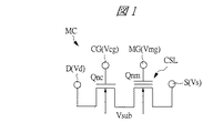
図1は、上記メモリセルMCの回路図を示している。メモリセルMCは、メモリセルMCのドレイン電極Dと、ソース電極Sとの間に、例えばメモリセル選択用のnMISQnc(以下、単に選択用のnMISQncという)と、メモリ用のnMISQnmとの2つのトランジスタを有している。選択用のnMISQncはコントロールゲート電極CGを有し、メモリ用のnMISQnmはメモリゲート電極MGおよび上記電荷蓄積層CSLを有している。符号のVdはドレイン電圧、Vcgはコントロールゲート電圧、Vmgはメモリゲート電圧、Vsはソース電圧、Vsubは基板電圧を示している。
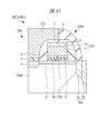
【0032】
図2は、上記メモリセルMCの基本的なデバイス断面の一例を示している。ここでは、コントロールゲート電極乗り上げ型のメモリセルMC1(MC)を例示している。半導体基板(以下、単に基板という)1Subは、例えばp型のシリコン(Si)単結晶からなり、その主面(デバイス形成面)にはメモリセルMC1の選択用のnMISQncと、メモリ用のnMISQnmとが配置されている。このメモリセルMC1のドレイン領域Drmおよびソース領域Srmは、例えばn−型の半導体領域2aと、その半導体領域2aよりも不純物濃度の高いn+型の半導体領域2bとを有している(LDD(Lightly Doped Drain)構造)。n−型の半導体領域2aは、メモリセルMCのチャネル領域側に配置され、n+型の半導体領域2bはメモリセルMCのチャネル領域側からn−型の半導体領域2a分だけ離れた位置に配置されている。このドレイン領域Drmとソース領域Srmとの間の基板1Subの主面上には、上記選択用のnMISQncのコントロールゲート電極CGと、上記メモリ用のnMISQnmのメモリゲート電極MGとが隣接して配置されている。
【0033】
コントールゲート電極CGおよびメモリゲート電極MGは、例えばn型の低抵抗なポリシリコンからなる。コントロールゲート電極CGの一部はメモリゲート電極MG側に乗り上げている。コントロールゲート電極CGと基板1Subの主面との間には、例えば厚さ2〜3nm程度の薄い酸化シリコン(SiO2等)からなるゲート絶縁膜3が設けられている。このゲート絶縁膜3の下方の基板1Subの主面には、p型の半導体領域4が形成されている。この半導体領域4は、選択用のnMISQncのチャネル形成用の半導体領域であり、この半導体領域4により選択用のnMISQncのしきい値電圧が所定の値に設定されている。半導体領域4は、選択用のnMISQncのしきい値電圧を上げる機能を有している。半導体領域4には、ホウ素(B)が導入されている。
【0034】
一方、メモリゲート電極MGと基板1Subの主面との間には、上記電荷蓄積層CSLが、その上下の絶縁膜5t,5bに挟まれた状態で設けられている。電荷蓄積層CSLは、例えば窒化シリコンからなり、その厚さは、例えば50nm以下である。ただし、電荷蓄積層CSLは窒化シリコンに限定されるものではなく種々変更可能であり、例えばアルミナ(Al2O3)等のように絶縁性のトラップ準位を形成できるような材料を用いることができる。絶縁膜5b,5tは、例えば酸化シリコン等からなる。絶縁膜5bの厚さは、例えば2〜6nm程度、絶縁膜5tの厚さは、例えば10〜17nm程度である。絶縁膜5tを酸窒化シリコン(SiON)で形成しても良い。
【0035】
また、絶縁膜5b、5tを、それぞれ窒素を含有した酸化シリコン膜として形成することもできる。これは、メモリ用のnMISQnmを形成した後に、選択用のnMISQncまたはメモリセル周辺のMIS形成領域に形成されるMISのゲート絶縁膜として酸化シリコン膜を形成する酸化工程において、シリコンからなる基板1Subと多結晶シリコンからなるメモリゲート電極MGが酸化され、それによって絶縁膜5b、5tの端部における膜厚が増加してしまうという問題がある。本実施の形態のようなメモリ用のnMISQnmでは、基板1Subから電荷蓄積層CSLへ電子を注入して書き込み動作を行ない、電荷蓄積層CSLからメモリゲート電極MGへ電子を引き抜くことで消去動作を行なうため、このようなメモリゲート電極MG端部での絶縁膜5b、5t膜厚の増加は、誤書き込み・誤消去の原因となる。したがって、絶縁膜5b、5tを、それぞれ窒素を含有した酸化シリコン膜とすることで、絶縁膜5b、5tの端部における過剰な酸化シリコン膜の形成を防止することが可能となる。
【0036】
具体的な実施方法としては、絶縁膜5b形成後に、例えば、酸窒化(NO)アニールを行ない、絶縁膜5bの基板1Sub側に窒素を導入する。これにより、他の酸化工程時に絶縁膜5b端部の膜厚の増加を防ぐことが可能となる。また、絶縁膜5t形成後に窒素プラズマ処理を行なうか、またはメモリゲート電極MGとなる導電膜の堆積後に酸窒化(NO)アニールを行なうことによって、絶縁膜5tの導電膜側に窒素を導入することができる。これにより、他の酸化工程時に絶縁膜5t端部の膜厚の増加を防ぐことが可能となる。
【0037】
更に、選択用のnMISQncまたはメモリセル周辺のMISのゲート絶縁膜(酸化シリコン膜)をCVD法によって形成することで、熱酸化工程に比べて成膜温度を低くすることができるので、絶縁膜5b、5tの端部における過剰な酸化シリコン膜の形成を、より阻害することが可能となる。
【0038】
上記絶縁膜5bの下方、p型の半導体領域4とソース領域Srmとの間の基板1Subの主面には、n型の半導体領域6が形成されている。この半導体領域6は、メモリ用のnMISQnmのチャネル形成用の半導体領域であり、この半導体領域6によりメモリ用のnMISQnmのしきい値電圧が所定の値に設定されている。半導体領域6は、メモリ用のnMISQnmのしきい値電圧を下げる機能を有している。半導体領域6には、例えばヒ素(As)またはリン(P)が導入されている。メモリゲート電極MGの上面には、例えば酸化シリコンからなる絶縁膜7が設けられている。
【0039】
また、メモリゲート電極MG、絶縁膜5t,5bおよび電荷蓄積層CSLの側面には、例えば酸化シリコンからなるサイドウォール8が形成されており、メモリゲート電極MGとコントロールゲート電極CGとの絶縁がなされている。このようなメモリセルMC1のコントロールゲート電極CGの両側面、絶縁膜7の上面一部およびソース領域Srm側のサイドウォール8の表面には、これを覆うようにサイドウォール9が形成されている。このサイドウォール9は、例えば酸化シリコンからなり、主として上記n−型の半導体領域2aを形成するための部材である。
【0040】
このようなメモリセルMC1において、データの記憶に寄与する電荷は、ホットエレクトロン注入により矢印Aで示す位置等で基板1Subから電荷蓄積層CSL中のトラップ準位に注入される。この電荷は離散的に蓄積されるため、電荷蓄積層CSLを取り囲む酸化膜(絶縁膜5b,5tやサイドウォール8)のどこか一部に欠陥が生じて異常リークがおきても、電荷蓄積層CSL中の電荷が全て抜けてしまうことがないため、データ保持の信頼度を向上させることができる。そして、このため、電荷蓄積層CSLの上下の絶縁膜5b,5tを薄膜化できるので、書き込みおよび消去動作の低電圧化を図ることができる。また、データの書き込み時はホットエレクトロン注入により基板1Subから電荷蓄積層CSL中に電子を注入するので、電子注入効率に優れ、高速、低電流の書き込みができる。一方、データの消去時はメモリゲート電極MG側に正の電圧を印加して電荷蓄積層CSL中の電子をメモリゲート電極MG側に引き抜く方式とするので、書き込みおよび消去動作の制御が容易であり、電源回路や周辺回路の簡素化(小規模化)が可能である。
【0041】
図3は、図1および図2のメモリセルMCのデータの読み出し動作Re、消去動作Erおよび書き込み動作Wr時の各部への印加電圧値の一例を示している。
【0042】
データの読み出し動作Reに際しては、選択したメモリセルMCのドレイン電極D(ドレイン領域Drm)に、例えば1V程度、コントロールゲート電極CGに、例えば1.5V程度、選択したメモリセルMCのソース電極S(ソース領域Srm)、メモリゲート電極MGおよび基板1Subに、例えば0(零)Vを印加して、メモリセルMCの選択用のnMISQncをオンする。この時、メモリ用のnMISQnmの電荷蓄積層CSL中の電子の有無によりメモリ用のnMISQnmのしきい値電圧が変化し、ドレイン領域Drmとソース領域Srmとの間に電流が流れたり、流れなかったりするので、これにより、記憶データを読み出す。
【0043】
また、データの消去動作Erに際しては、選択したメモリセルMCのドレイン電極D(ドレイン領域Drm)、ソース電極S(ソース領域Srm)および基板1Subに、例えば0(零)V、コントロールゲート電極CGに、例えば1.5V程度、メモリゲート電極MGに、例えば14V程度を印加する。これにより、電荷蓄積層CSL中の電子をトンネル放出によりメモリゲート電極MG側に逃がし、データを消去する。
【0044】
さらに、データの書き込みは、ソースサイド・ホットエレクトロン注入方式を採用している。データの書き込み動作Wrに際しては、選択したメモリセルMCのドレイン電極D(ドレイン領域Drm)および基板1Subに、例えば0(零)V、コントロールゲート電極CGに、例えば1.5V程度、メモリゲート電極MGに、例えば12V程度、選択したメモリセルMCのソース電極S(ソース領域Srm)に、例えば6V程度を印加する。これにより、メモリセルMCのチャネルで発生したホットエレクトロンを電荷蓄積層CSLに注入し、データを書き込む。
【0045】
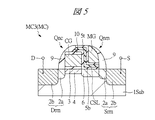
図4および図5は、スプリットゲート電極型のメモリセルMCの基本的なデバイス断面の他の例を示している。図4はメモリゲート電極乗り上げ型のメモリセルMC2(MC)を例示し、図5はサイドウォール方式メモリゲート電極乗り上げ型のメモリセルMC3(MC)を例示している。図4および図5のメモリセルMC2,MC3では、メモリゲート電極MGの一部がコントロールゲート電極CG側に乗り上げているが、コントロールゲート電極CG上面上の酸化シリコン等からなる絶縁膜10、絶縁膜5b,5tおよび電荷蓄積層CSL等によりコントロールゲート電極CGとメモリゲート電極MGとの絶縁がなされている。この場合もデータの読み出し、書き込みおよび消去動作は上記したのと同じなので説明を省略する。以上のようなメモリセルを有する半導体装置は、例えばIC(Integrated circuit)カード(メモリカード)に使用されている。
【0046】
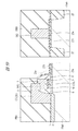
次に、上記図2、図4および図5に示したスプリットゲート型のメモリセルMC(MC1〜MC3)について本発明者が初めて見出した課題を図6および図7により説明する。
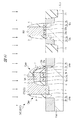
【0047】
図6は上記図2のスプリットゲート電極型のメモリセルMC1の形成工程中の基板1Subの要部断面図を示している。この基板1Sub(この段階では平面略円形状のウエハ)の主面には、n型の半導体領域6が形成されている。また、この基板1Subの主面には、絶縁膜5b、電荷蓄積層CSL、絶縁膜5t、メモリゲート電極MGおよび絶縁膜7の積層パターンが形成されている。そして、その積層パターンの側面には、例えば酸化シリコンからなるサイドウォール8が形成されている。上記メモリセルMC1の形成工程では、まず、このような基板1Subの主面上に、図7に示すように、選択用のnMISQnc(図2参照)の形成領域が露出され、それ以外の領域が覆われるようなフォトレジストパターン(以下、単にレジストパターンという)PR1を形成する。続いて、そのレジストパターンPR1、サイドウォール8およびメモリゲート電極MGの一部をマスクとして、例えばホウ素(B)をイオン注入法により基板1Subの主面に導入する。これにより、基板1Subの主面にp型の半導体領域4をメモリゲート電極MGに対して自己整合的に形成する。この時、メモリセルMC1の動作安定性の観点からは選択用のnMISQncのしきい値電圧を高く保ちたいので、ホウ素の導入量を、既に基板1Subの主面に形成されている上記n型の半導体領域6の導電型が打ち消される程度に導入する必要がある。このため、p型の半導体領域4には多量の不純物が打ち込まれることになるので、その半導体領域4での総合の不純物濃度(半導体領域4,6の各々の形成用の不純物濃度の和)が高くなる。
【0048】
このように、図2、図4および図5のスプリットゲート電極型のメモリセルMC1〜MC3では、選択用のnMISQncとメモリ用のnMISQnmとが隣接しているため、nMISQnc,Qnmのチャネル形成用の半導体領域を形成するには、そのいずれか一方のチャネル形成用の半導体領域を形成するための不純物を基板1Subに打ち込んだ後に、それを打ち消すように反対導電型の不純物を打ち込むことにより他方のチャネル形成用の半導体領域を形成する必要がある。このため、どちらかのチャネル形成用の半導体領域には多量の不純物が打ち込まれることになるので、その多量の不純物が打ち込まれたチャネル形成用の半導体領域の総合の不純物濃度が高くなる。その結果、キャリアの移動度の低下(ドレイン電流Idsの低下)やしきい値電圧のばらつきの増大等のような電気的特性の劣化が生じる。
【0049】
そこで、本実施の形態1では、選択用のMISとメモリ用のMISとの2つのMISを有するスプリットゲート電極型のメモリセルMCの形成工程において、一方のMISのチャネル形成用の半導体領域をエッチングしてから、他方のMISのチャネル形成用の半導体領域を形成する。これにより、他方のMISのチャネル形成用の半導体領域の不純物濃度を下げることができるので、キャリアの移動度を向上させることができ、メモリセルMCでのドレイン電流Idsを増大させることができる。したがって、スプリットゲート電極型のメモリセルMCの動作速度(データの読み出し速度)を向上させることができる。また、しきい値電圧のバラツキを低減できるので、スプリットゲート型のメモリセルMCの動作信頼性を向上させることができる。
【0050】
この具体例を図8〜図19の半導体装置の製造工程中におけるメモリ領域の基板1Subの要部断面図により説明する。ここでは、図2のメモリセルMC1への適用例を説明する。
【0051】
まず、図8に示すように、例えばp型のシリコン(Si)単結晶からなる基板1Sub(この段階では平面略円形状の半導体ウエハ)の主面に、例えばヒ素(As)をイオン注入法により導入する。これにより、基板1Subの主面に、メモリ用のnMISQnm(図2参照)のチャネル形成用のn型の半導体領域6を形成する。本実施の形態1では、後述する工程で基板1Subの主面を若干エッチングしてn型の半導体領域6を部分的に除去するエッチング工程があるが、上記半導体領域6を形成するための不純物イオンがあまり深い位置まで打ち込まれていると、上記エッチング工程時に基板1Subのエッチング量を大きくせざるを得なくなってしまうので、半導体領域6を形成するための不純物イオンの打ち込み深さを浅くした方が好ましい。この時の不純物イオンの打ち込みエネルギーは、例えば20〜40keV程度である。また、この時の不純物イオンの打ち込み深さ(不純物濃度が最も高くなる深さ)は、例えば10〜20nm程度である。また、不純物イオンのドーズ量は、例えば1×10¹⁴/cm2程度である。不純物としてリンを用いることもできるが、ヒ素を用いたのは、リンよりも原子量(質量)の重いヒ素を用いることにより、同じ打ち込みエネルギーでも基板1Subの浅い位置に半導体領域6を形成でき、浅い位置に半導体領域6を形成するのが容易だからである。
【0052】
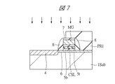
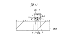
次いで、図9に示すように、基板1Subの主面上に、例えば酸化シリコンからなる絶縁膜5b、窒化シリコンからなる電荷蓄積層CSL、酸化シリコンからなる絶縁膜5t、低抵抗ポリシリコンからなるメモリゲート形成用の導体膜11および酸化シリコンからなる絶縁膜7を酸化、もしくはCVD(Chemical Vapor Deposition)法により下層から順に堆積した後、これら積層膜をフォトリソグラフィ(以下、単にリソグラフィという)技術およびエッチング技術によりパターニングすることにより、図10に示すように、絶縁膜5b、電荷蓄積層CSL、絶縁膜5t、メモリゲート電極MG(11)および絶縁膜7の積層パターンを形成する。続いて、基板1Subの主面上に、例えば酸化シリコンからなる絶縁膜をCVD法等によって堆積した後、これを異方性のドライエッチング法によりエッチバックすることにより、図11に示すように、上記積層パターンの側面にサイドウォール8を形成する。
【0053】
次いで、図12に示すように、基板1Subの主面上に、選択用のnMIS形成領域側が露出されるようなレジストパターンPR2を形成した後、レジストパターンPR2、サイドウォール8および絶縁膜8をエッチングマスクとして、サイドウォール8の材料と基板1Subの材料とのエッチング選択比が大きくなるような条件でエッチング処理を施すことにより、選択用のnMIS形成領域の基板1Subの主面を部分的にエッチングして窪み13を形成する。これにより、選択用のnMIS形成領域のn型の半導体領域6を除去する。この時、サイドウォール8をエッチングマスクとしているので、基板1Subの一部を位置合わせ良く選択的に除去することができる。この時のエッチング方法としては、例えばドライエッチング法を用いている。ただし、ウエットエッチング法を用いても良い。ウエットエッチングを用いた場合、基板1Subにあまり損傷を与えることなく基板1Subの一部を除去できる。また、ドライエッチング処理を施した後、若干のウエットエッチング処理を施すことにより、ドライエッチング時に生じた基板1Subの損傷層を除去しても良い。これにより、選択用のnMISの電気的特性を向上させることができる。窪み13の深さは、あまり深いと段差の原因となるので、例えば50nm以下が好ましく、具体的には、例えば20nm程度とされている。
【0054】
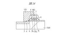
次いで、図13に示すように、レジストパターンPR2、サイドウォール8およびメモリゲート電極MGをマスクとして、基板1Subの主面に、例えば二フッ化ホウ素(BF2)をイオン注入することにより、選択用のnMISのチャネル形成用のp型の半導体領域4を形成する。この時の不純物イオンの打ち込みエネルギーは、例えば40〜100keV程度である。本実施の形態1では、選択用のnMIS形成領域の基板1Subの主面が削られn型の半導体領域6が除去されているので、窪み13を形成しない場合と比較して、選択用のnMISのチャネル形成用のp型の半導体領域4の不純物濃度を下げることができる。このため、キャリア(電子)の移動度を向上させることができ、メモリセルMC1でのドレイン電流Idsを増大させることができる。したがって、スプリットゲート電極型のメモリセルMC1の動作速度(データの読み出し速度)を向上させることができる。また、選択用のnMISのしきい値電圧のバラツキを低減できるので、スプリットゲート電極型のメモリセルMC1の動作信頼性を向上させることができる。
【0055】
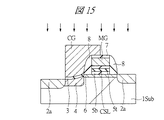
次いで、図14に示すように、基板1Subに対して酸化処理を施すことにより、基板1Subの主面上に、例えば酸化シリコンからなるゲート絶縁膜3を形成した後、その基板1Subの主面上に、例えば低抵抗ポリシリコンからなる導体膜をCVD法により堆積し、さらにその導体膜をリソグラフィ技術およびドライエッチング技術によりパターニングすることにより、コントロールゲート電極CGを形成する。続いて、図15に示すように、コントロールゲート電極CGおよびメモリゲート電極MGをマスクとして、例えばヒ素またはリンを基板1Subの主面にイオン注入することにより、基板1Subの主面にn−型の半導体領域2aをコントールゲート電極CGおよびメモリゲート電極MGに対して自己整合的に形成する。
【0056】
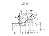
次いで、基板1Subの主面上に、例えば酸化シリコンからなる絶縁膜をCVD法により堆積した後、これを異方性のドライエッチング法によりエッチバックすることにより、図16に示すように、コントロールゲート電極CGの両側面、絶縁膜7上およびサイドウォール8の表面上に、サイドウォール9を形成する。続いて、図17に示すように、サイドウォール9およびコントロールゲート電極CGをマスクとして、例えばヒ素またはリンを基板1Subの主面にイオン注入することにより、基板1Subの主面にn+型の半導体領域2bをコントールゲート電極CGおよびメモリゲート電極MGに対して自己整合的に形成する。このようにしてメモリセルMC1のドレイン領域Drmおよびソース領域Srmを形成し、選択用のnMISQncおよびメモリ用のnMISQnmを形成する。その後、図18に示すように、基板1Subの主面部およびコントロールゲート電極CGの上面部に、例えばコバルトシリサイド(CoSix)等のようなシリサイド層14をサリサイド(Salicide:Self Align silicide)プロセスにより形成する。
【0057】
次いで、図19に示すように、基板1Subの主面上に、例えば酸化シリコンからなる絶縁膜15をCVD法により堆積した後、絶縁膜15にコンタクトホールCNTを形成する。続いて、コンタクトホールCNT内にプラグPLGを形成する。プラグPLGは、例えばチタン(Ti)および窒化チタン(TiN)の積層膜からなる薄いバリア膜と、そのバリア膜に包まれるように形成されたタングステン(W)またはアルミニウム(Al)等からなる相対的厚い導体膜とを有している。その後、絶縁膜15上に、例えばタングステンまたはアルミニウム(Al)等からなる第1層配線M1を形成する。これ以降は、通常の半導体装置の製造工程を経て不揮発性メモリを有する半導体装置を製造する。
【0058】
(実施の形態2)
本実施の形態2では、前記実施の形態1の変形例であって、メモリゲート電極の両側の基板1Sub部分をエッチングする例を、図20〜図22の半導体装置の製造工程中の基板1Subの要部断面図により説明する。
【0059】
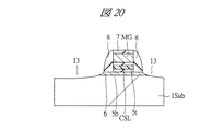
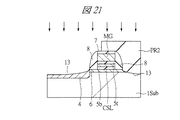
まず、前記実施の形態1の図8〜図11で説明した工程を経た後、前記図12で説明したのと同様のエッチング処理を基板1Subに施すことにより、図20に示すように、メモリゲート電極MGおよびサイドウォール8の形成領域から露出される基板1Subの主面部に窪み13を形成する。ここでは、メモリゲート電極MGおよびサイドウォール8の形成領域の両側を除去する。すなわち、メモリセルのソース領域の形成部分の半導体領域6も除去してしまう。続いて、図21に示すように、基板1Subの主面上に、選択用のnMIS形成領域側が露出されるようなレジストパターンPR2を形成した後、レジストパターンPR2、サイドウォール8および絶縁膜8をマスクとして、基板1Subの主面に、例えば二フッ化ホウ素(BF2)をイオン注入することにより、選択用のnMISのチャネル形成用のp型の半導体領域4を形成する。この時の条件は、前記図13で説明したのと同じである。また、本実施の形態2でも、前記図13で説明したのと同様の効果を得ることができる。その後、前記実施の形態1と同様にして、図22に示すように、メモリセルMC1(MC)を形成する。
【0060】
本実施の形態2では、メモリセルMC1のソース領域Srmの形成部分でも窪み13を形成し、n型の半導体領域6の層を除去しているので、ドレイン領域Drmおよびソース領域Srmのn−型の半導体領域2aおよびn+型の半導体領域2bの不純物濃度も低減できる。また、窪み13を形成しない場合と比較して、n−型の半導体領域2aおよびn+型の半導体領域2bの濃度調整を容易にすることができる。
【0061】
(実施の形態3)
前記実施の形態1,2の方法は、前記図4および図5のメモリセルMC2,MC3にも適用できる。そこで、本実施の形態3では、前記図4のメモリセルMC2に前記実施の形態2の方法を適用した例を図23〜図31の半導体装置の製造工程中の要部断面図により説明する。
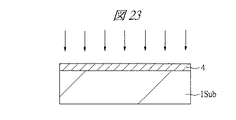
【0062】
まず、図23に示すように、例えばp型のシリコン(Si)単結晶からなる基板1Sub(前記半導体ウエハ)の主面に、例えば二フッ化ホウ素(BF2)をイオン注入法により導入する。これにより、基板1Subの主面に、選択用のnMISQnc(図4参照)のチャネル形成用のp型の半導体領域4を形成する。本実施の形態3では、後述する工程で基板1Subの主面を若干エッチングしてp型の半導体領域4を部分的に除去するエッチング工程があるので、前記実施の形態1のn型の半導体領域6と同様の理由から、p型の半導体領域4を形成するための不純物イオンの打ち込み深さを浅くした方が好ましい。この時の不純物イオンの打ち込みエネルギーは、例えば40〜100keV程度である。また、この時の不純物イオンの打ち込み深さ(不純物濃度が最も高くなる深さ)は、例えば40〜100nm程度である。また、不純物イオンのドーズ量は、例えば1×10¹⁴/cm2程度である。不純物としてホウ素を用いることもできるが、二フッ化ホウ素を用いたのは、ホウ素よりも原子量(質量)の重い二フッ化ホウ素を用いることにより、同じ打ち込みエネルギーでも基板1Subの浅い位置に半導体領域4を形成でき、浅い位置に半導体領域4を形成するのが容易だからである。
【0063】
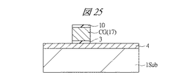
続いて、図24に示すように、基板1Subに対して酸化処理を施すことにより、基板1Subの主面上に、例えば酸化シリコンからなるゲート絶縁膜3を形成した後、その基板1Subの主面上に、例えば低抵抗ポリシリコンからなる導体膜17をCVD法により堆積し、さらにその導体膜17上に、例えば酸化シリコンからなる絶縁膜10をCVD法により堆積する。その後、ゲート絶縁膜3、導体膜17および絶縁膜10の積層膜をリソグラフィ技術およびドライエッチング技術によりパターニングすることにより、図25に示すように、コントロールゲート電極CGを形成する。
【0064】
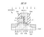
次いで、前記図12で説明したのと同様のエッチング処理を基板1Subに施すことにより、図26に示すように、コントロールゲート電極CGの形成領域から露出される基板1Subの主面部に窪み13を形成する。ここでは、コントロールゲート電極CGの形成領域の両側の基板1Subの表層を除去する。すなわち、メモリセルのメモリ用のnMIS形成領域、ソース領域およびドレイン領域の形成部分のp型の半導体領域4も除去してしまう。続いて、図27に示すように、コントロールゲート電極CGをマスクとして、基板1Subの主面に、例えばヒ素またはリンをイオン注入することにより、メモリ用のnMISのチャネル形成用のn型の半導体領域6を形成する。この時の不純物イオンの打ち込みエネルギーは、例えば20〜40keV程度である。本実施の形態3では、メモリ用のnMIS形成領域の基板1Subの主面が削られp型の半導体領域4が除去されているので、メモリ用のnMISのチャネル形成用のn型の半導体領域6の不純物濃度を下げることができる。このため、キャリア(電子)の移動度を向上させることができ、メモリセルMC2でのドレイン電流Idsを増大させることができる。したがって、スプリットゲート電極型のメモリセルMC2の動作速度(データの読み出し速度)を向上させることができる。また、窪み13を形成しない場合と比較して、メモリ用のnMISのしきい値電圧のバラツキを低減できるので、スプリットゲート型のメモリセルMC2の動作信頼性を向上させることができる。
【0065】
次いで、図28に示すように、基板1Subの主面上に、前記絶縁膜5b、電荷蓄積層CSL絶縁膜5tおよびメモリゲート形成用の導体膜11をCVD法により下層から順に堆積した後、これら積層膜をリソグラフィ技術およびエッチング技術によりパターニングすることにより、図29に示すように、絶縁膜5b、電荷蓄積層CSL、絶縁膜5tおよびメモリゲート電極MG(11)の積層パターンを形成する。続いて、コントロールゲート電極CGおよびメモリゲート電極MGをマスクとして、例えばヒ素またはリンを基板1Subの主面にイオン注入することにより、基板1Subの主面にn−型の半導体領域2aをコントールゲート電極CGおよびメモリゲート電極MGに対して自己整合的に形成する。その後、基板1Subの主面上に、例えば酸化シリコンからなる絶縁膜をCVD法により堆積した後、これを異方性のドライエッチング法によりエッチバックすることにより、図30に示すように、コントロールゲート電極CGの片側面、絶縁膜10上およびメモリゲート電極MGの両側面に、サイドウォール9を形成する。続いて、サイドウォール9およびメモリゲート電極MGをマスクとして、例えばヒ素またはリンを基板1Subの主面にイオン注入することにより、基板1Subの主面にn+型の半導体領域2bをコントールゲート電極CGおよびメモリゲート電極MGに対して自己整合的に形成する。このようにしてメモリセルMC2のドレイン領域Drmおよびソース領域Srmを形成し、選択用のnMISQncおよびメモリ用のnMISQnmを形成する。その後、図31に示すように、前記実施の形態1と同様に、サリサイドプロセスを経て基板1Subの主面部およびコントロールゲート電極CGの上面部にシリサイド層14を形成し、絶縁膜15を堆積し、コンタクトホールCNTを形成し、プラグPLGを形成し、第1層配線M1を形成する。
【0066】
本実施の形態3では、メモリセルMC2のドレイン領域Drmおよびソース領域Srmの形成部分でも窪み13を形成し、p型の半導体領域4の層を除去しているので、ドレイン領域Drmおよびソース領域Srmのn−型の半導体領域2aおよびn+型の半導体領域2bの不純物濃度も低減できる。また、窪み13を形成しない場合と比較して、そのn−型の半導体領域2aおよびn+型の半導体領域2bの濃度調整を容易にすることができる。
【0067】
(実施の形態4)
本実施の形態4は、前記スプリットゲート電極型のメモリセルについて本発明者が初めて見出した他の問題を解決するための一例を説明するものである。その問題は、メモリセルの選択用のMISのソース・ドレイン用の半導体領域がコントロールゲート電極に対してオフセットになるという問題である。
【0068】
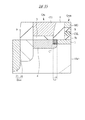
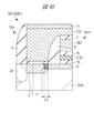
まず、その問題を図32および図33により説明する。図32はメモリセルMC1の要部断面図、図33は図32の破線で囲んだ領域Bの拡大断面図を示している。メモリセルMC1の場合、選択用のnMISQncのチャネル形成用のp型の半導体領域4を、メモリ用のnMISQnmのチャネル形成用のn型の半導体領域6の形成後に形成するので、選択用のnMISQnmとメモリ用のnMISQnmとの境界領域では、p型の半導体領域4の一部がn型の半導体領域6側に拡散する。そのp型の半導体領域4がn型の半導体領域6側に拡散した領域Cでは、本来、n型であった領域が、p型またはp型に近い導電型に変わってしまう場合がある。その結果、選択用のnMISQncのコントロールゲート電極CGから見ると、選択用のnMISQncのソース・ドレイン領域となるn型の半導体領域6が長さL1だけ離れてしまったような形となる。すなわち、ドレイン電流Idsを律則するコントロールゲート電極CGがゲート絶縁膜3を介して平面的に重ならない部分(領域C)が生じる。このようなオフセット領域が生じると、ドレイン電流Idsが低下し、メモリセルMC1の動作速度が低下する問題が生じる。
【0069】
そこで、本実施の形態4では、選択用のMISのチャネル形成用の半導体領域の端部が、メモリ用のMISのメモリゲート電極の側面に形成されたサイドウォールの側面から離れるようなスペーサを、メモリゲート電極の側面のサイドウォールの側面に形成した後に、選択用のMISのチャネル形成用の半導体領域を形成するための不純物を基板1Subに導入する。これにより、選択用のMISのソース・ドレイン領域となる半導体領域(メモリ用のMISのチャネル形成用の半導体領域)の端部がコントロールゲート電極下で確実に重なるようにすることができるので、スプリットゲート型のメモリセルのドレイン電流Idsを向上させることができる。したがって、スプリットゲート型のメモリセルの動作速度(データの読み出し速度)を向上させることができる。この具体例を図34〜図39の半導体装置の製造工程中におけるメモリ領域の基板1Subの要部断面図により説明する。
【0070】
まず、前記実施の形態1の図8〜図11で説明した工程を経た後、図34に示すように、基板1Sub(半導体ウエハ)の主面上に、上記スペーサ用の絶縁膜19を堆積する。絶縁膜19は、例えば酸化シリコンからなり、その厚さは、例えば30nm程度である。本実施の形態4では、この絶縁膜19を、例えばTEOS(Tetraethoxysilane)と酸素(O2)との混合ガスを用いたCVD法等により堆積した。また、下層の絶縁膜7およびサイドウォール8形成用の酸化シリコン膜は、例えばモノシラン(SiH4)と酸素(O2)との混合ガスを用いたCVD法により堆積した後、その酸化シリコン膜の緻密化のためにアニール処理を施すことで形成されている。このようにすることで、後述するように絶縁膜19をウエットエッチング処理により除去するときに、絶縁膜19のエッチングレートを、同じ酸化シリコンからなる絶縁膜7およびサイドウォール8の2倍程度にまでできるので、絶縁膜19を選択的に除去することができる。ただし、絶縁膜19の材料として窒化シリコンを用いても良い。この場合も絶縁膜19をエッチング除去するときに酸化シリコンとのエッチング選択比を高くとることができる。
【0071】
続いて、図35に示すように、基板1Subの主面上に、前記実施の形態1と同様にレジストパターンPR2を形成した後、前記実施の形態1の図13で説明したのと同様に、例えば二フッ化ホウ素(BF2)またはホウ素(B)をイオン注入することにより、選択用のnMISのチャネル形成用のp型の半導体領域4を形成する。この時、本実施の形態4では、選択用のnMIS形成領域側のサイドウォール8の側面に被着された絶縁膜19がマスクとなり、p型の半導体領域4のメモリゲート電極CG側の端部が、選択用のnMIS形成領域側のサイドウォール8の側面から絶縁膜19の厚さ分だけ離れたところに位置するようになる。
【0072】
その後、レジストパターンPR2を除去後、絶縁膜19を、図36に示すように、ウエットエッチング法により選択的に除去する。続いて、図37に示すように、前記実施の形態1と同様に、ゲート絶縁膜3およびコントロールゲート電極CGを形成した後、例えばヒ素またはリンを基板1Subにイオン注入してn−型の半導体領域2aを形成する。その後、図38および図39に示すように、前記実施の形態1と同様に、選択用のnMISQncおよびメモリ用のnMISQnmを形成し、スプリットゲート電極型のメモリセルMC1を形成する。
【0073】
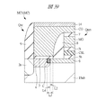
本実施の形態4では、図39に示すように、n型の半導体領域6の端部がサイドウォール8の側面から長さL2だけコントロールゲート電極CG下側に突き出すように延在している。すなわち、メモリセルMC1の電流を律則するコントロールゲート電極CGがゲート絶縁膜3を介して確実にn型の半導体領域6(選択用のnMISQncのソース・ドレイン領域)の端部に重なるようにすることができる。したがって、スプリットゲート電極型のメモリセルMC1のドレイン電流Idsを向上させることができるので、スプリットゲート電極型のメモリセルMC1の動作速度(データの読み出し速度)を向上させることができる。長さL2は、上記絶縁膜19の厚さで制御できる。したがって、コントロールゲート電極CGがゲート絶縁膜3を介してn型の半導体領域6の端部に重なる重なり量を比較的容易に設定することができる。長さL3は絶縁膜19の厚さを示している。長さL3から長さL2を引いた長さL4は、p型の半導体領域4がn型の半導体領域6側に拡散した長さを示している。
【0074】
ただし、本実施の形態4では、n型の半導体領域6がコントロールゲート電極CG下に突き出しコントロールゲート電極CGがゲート絶縁膜3を介してn型の半導体領域6の端部に重なっている場合について説明したが、本実施の形態4は、選択用のnMISQncのソース・ドレイン領域であるn型の半導体領域6の端部がコントロールゲート電極CGの端部から離れていなければ良く、図40に示すように、コントロールゲート電極CGがゲート絶縁膜3を介してn型の半導体領域6の端部と重なっていないが、n型の半導体領域6の端部がサイドウォール8の側面位置とほぼ一致しており、コントロールゲート電極CGの端部から離れていない構造を排除するものではない。なお、図40の長さL5は、絶縁膜19の厚さであり、また、p型の半導体領域4がn型の半導体領域6側に拡散した長さでもある。
【0075】
また、本実施の形態4と前記実施の形態1,2とを組み合わせても良い。すなわち、基板1Subの主面に窪み13を形成した後、絶縁膜19を堆積し、その後、p型の半導体領域4を形成するための不純物を導入する。
【0076】
また、前記絶縁膜19を他の工程で用いる絶縁膜と兼用しても良い。この場合、工程の兼用ができるので、半導体装置の製造時間の短縮およびコストの低減が可能となる。
【0077】
(実施の形態5)
本実施の形態5は、前記スプリットゲート電極型のメモリセルについて本発明者が初めて見出した他の問題を解決するための一例を説明するものである。その問題は、乗り上げている側のゲート電極をパターニングする工程で、乗り上げていないゲート電極の側面に、乗り上げている側のゲート電極の一部が残され、それを除去する際に基板の主面をエッチングしてしまうという問題である。
【0078】
まず、その問題を図41〜図43により説明する。図41〜図43はコントロールゲート電極のパターニング工程中の基板1Subの要部断面図を示している。図41に示すように、基板1Subの主面にゲート絶縁膜3を形成した後、基板1Subの主面上に、コントロールゲート電極形成用の低抵抗ポリシリコン等からなる導体膜21をCVD法等によって堆積し、さらにその上にコントロールゲート電極形成用のレジストパターンPR3を形成する。続いて、レジストパターンPR3をエッチングマスクとして異方性のドライエッチング処理を施すことにより、図42に示すように、コントロールゲート電極CGを形成する。この時、メモリゲート電極MG側面のサイドウォール8の側面に導体膜21aが残される場合がある。そこで、その残された導体膜21aを除去するため、図43に示すように、導体膜21aが露出されるようなレジストパターンPR4を形成し、エッチング処理により導体膜21aを除去する。ところが、この時、導体膜21aはポリシリコンからなるので、下層のシリコンからなる基板1Subの主面も部分的にエッチングされ、基板1Subの主面が荒れてしまう結果、メモリセルのドレイン電流Idsが低下する場合がある。
【0079】
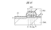
そこで、本実施の形態5では、ゲート電極が乗り上げない側の基板上に保護膜を形成する工程を有するものである。これにより、乗り上げる側のゲート電極の加工時に生じたエッチ残りを除去する際に、上記保護膜により基板1Subの主面が保護されるので、基板1Subの主面がエッチングされるのを防止できる。この具体例を図44〜図52の半導体装置の製造工程中におけるメモリ領域の基板1Subの要部断面図により説明する。
【0080】
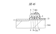
まず、前記実施の形態1の図8〜図11で説明した工程を経た後、図44に示すように、基板1Sub(半導体ウエハ)の主面上に、レジストパターンPR2を形成し、例えば二フッ化ホウ素(BF2)またはホウ素(B)をイオン注入することにより、p型の半導体領域4を形成する。続いて、レジストパターンPR2を除去した後、図45に示すように、基板1Subの主面上に、例えば酸化シリコンまたは窒化シリコンからなる厚さ20nm程度の絶縁膜23を形成する。その後、絶縁膜23上に、上記p型の半導体領域4の形成時に用いたレジストパターン2と同じレジストパターンPR5を形成した後、これをエッチングマスクとして絶縁膜23をエッチングすることにより、図46に示すように、絶縁膜23のパターンを形成する。絶縁膜23のパターンは、絶縁膜7の上面の一部と片側のサイドウォール8の表面と、メモリセルのソース領域側の基板1Subの上面とを覆うように形成されている。
【0081】
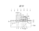
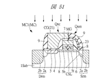
次いで、図47に示すように、基板1Subの主面上に、上記ゲート絶縁膜3を形成した後、その上に、例えば低抵抗ポリシリコンからなる導体膜21をCVD法等によって堆積する。続いて、導体膜21上に、コントロールゲート電極形成用のレジストパターンPR3を形成した後、これをエッチングマスクとして、導体膜21をパターニングすることにより、図48に示すように、コントロールゲート電極CGを形成する。この時、メモリゲート電極MGの片側側面のサイドウォール8の側面下部側に導体膜21aが残される。本実施の形態5では、導体膜21aが上記絶縁膜23上に残される。そこで、基板1Subの主面上に、導体膜21aを除去するためのレジストパターンPR4をリソグラフィ技術により形成した後、これをエッチングマスクとして、エッチング処理を施すことにより、導体膜21aを図49に示すように除去する。この時、本実施の形態5では、ポリシリコンと絶縁膜23とのエッチング選択比を大きくとり、ポリシリコンの方が絶縁膜23よりもエッチングされ易い条件でエッチング処理を施す。この時、ポリシリコンからなるエッチ残りの導体膜21aの下層(導体膜21aと基板1Subとの間)に、ゲート絶縁膜3よりも厚い絶縁膜23が設けられているので、基板1Subの主面が保護され、基板1Subの主面がエッチングされないようにすることができる。すなわち、エッチ残りの導体膜2aの除去に起因する基板1Subの荒れを防止できる。したがって、スプリットゲート電極型のメモリセルのドレイン電流Idsの低下を防止できるので、スプリットゲート電極型のメモリセルの高速動作(データの高速読み出し)を維持できる。
【0082】
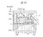
次いで、レジストパターンPR4を除去後、図50に示すように、基板1Subに、例えばリンまたはヒ素等のような不純物をイオン注入して、n−型の半導体領域2aをコントロールゲート電極CGおよびメモリゲート電極MGに対して自己整合的に形成する。続いて、図51に示すように、前記実施の形態1と同様に、サイドウォール9を形成した後、基板1Subの主面にn+型の半導体領域2bをコントールゲート電極CGおよびメモリゲート電極MGに対して自己整合的に形成する。このようにしてメモリセルMC1のドレイン領域Drmおよびソース領域Srmを形成し、選択用のnMISQncおよびメモリ用のnMISQnmを形成する。その後、図52に示すように、前記実施の形態1と同様に、サリサイドプロセスによりシリサイド層14を形成した後、絶縁膜15の堆積工程、コンタクトホールCNTの形成工程、プラグPLGの形成工程、第1層配線M1の形成工程を経て半導体装置を製造する。
【0083】
本実施の形態5と前記実施の形態1,2とを組み合わせても良い。すなわち、基板1Subの主面に窪み13を形成した後、p型の半導体領域4を形成する。続いて、絶縁膜23を堆積した後、コントロールゲート電極CGを形成する。
【0084】
また、本実施の形態5と前記実施の形態4とを組み合わせても良い。この場合、絶縁膜19,23を別々に堆積して各々の目的を達成させるようにしても良いが、保護用の絶縁膜23を前記実施の形態4のp型の半導体領域4を形成する際のスペーサ用の絶縁膜19として用いても良い。すなわち、図8〜図11の工程後、基板1Subの主面上に絶縁膜23を堆積し、さらに、前記実施の形態4と同様に不純物を導入してp型の半導体領域4を形成する。これ以降は上記図45以降で説明したのと同じである。この場合、保護用の絶縁膜23とスペーサ用の絶縁膜19とを別々に堆積する場合に比べて半導体装置の製造工程を低減でき、半導体装置の製造時間の短縮およびコストの低減が可能となる。
【0085】
(実施の形態6)
本実施の形態6は、前記実施の形態5の変形例であって、前記保護用の絶縁膜23を同一基板上の他のMISのゲート絶縁膜により形成する場合の一例を説明する。本実施の形態6によれば、工程の兼用ができるので、半導体装置の製造時間の短縮およびコストの低減が可能となる。
【0086】
図53〜図61は、本実施の形態6の半導体装置の製造工程中の基板1Subの要部断面図であって、各図の左側はメモリ領域の要部断面図を示し、右側は周辺回路用の高耐圧nMIS形成領域の要部断面図を示している。
【0087】
図53は、前記図8〜図11で説明した工程後、前記図44で説明した工程を経た後の基板1Sub(半導体ウエハ)の要部断面図を示している。また、図53の右側において、基板1Subの主面には、例えばSGI(Shallow Groove Isolation)と称する溝型の分離部25が形成されている。この分離部25は、基板1Subに掘られた溝内に、例えば酸化シリコン膜が埋め込まれることで形成されている。この分離部25により活性領域が規定されている。
【0088】
まず、このような基板1Subに対して酸化処理を施すことにより、図54に示すように、高耐圧nMISのゲート絶縁膜23aを基板1Subの主面に形成する。ゲート絶縁膜23aは、例えば厚さ2〜8nm程度の酸化シリコンからなり、高耐圧nMIS形成領域のみならず、メモリ領域の基板1Subの主面にも形成されている。続いて、図55に示すように、基板1Subの主面上に、例えば厚さ13nm程度の酸化シリコンからなる絶縁膜23bをCVD法等により堆積した後、絶縁膜23bの膜質を向上させるべくアニール処理を施す。絶縁膜23a,23bは、高耐圧nMISのゲート絶縁膜となる。絶縁膜23bを堆積することにより、高耐圧nMISのゲート絶縁耐圧を向上させることができる。その後、基板1Subの主面上に、メモリ領域の選択用のnMIS形成領域が露出され、高耐圧nMIS形成領域を覆うようなレジストパターンPR6をリソグラフィ技術により形成した後、これをエッチングマスクとしてエッチング処理を施すことにより、図56に示すように、絶縁膜23a,23bをパターニングする。メモリ領域の選択用のnMIS形成領域では、絶縁膜23aが除去され、基板1Subの主面が露出される。この後、前記実施の形態1のように選択用のnMIS形成領域の基板1Subの主面を部分的にエッチングして窪み13を形成してもよいのは勿論である。
【0089】
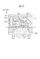
次いで、図57に示すように、基板1Subに対して酸化処理を施すことにより、基板1Subの主面上に、例えば酸化シリコンからなるゲート絶縁膜3を形成する。このゲート絶縁膜3は、選択用のnMIS等のような低耐圧のMISのゲート絶縁膜となる。ゲート絶縁膜3の厚さは、上記高耐圧nMISのゲート絶縁膜23a,23bよりも薄く、例えば2〜5nm程度である。続いて、基板1Subの主面上に、例えば低抵抗ポリシリコンからなる導体膜21をCVD法等により堆積した後、その上にレジストパターンPR7をリソグラフィ技術により形成する。レジストパターンPR7は、メモリ領域のコントロールゲート電極形成領域と、高耐圧nMIS形成領域のゲート電極形成領域を覆い、それ以外が露出されるようなパターンとされている。その後、レジストパターンPR7をエッチングマスクとして、エッチング処理により導体膜21をパターニングすることにより、図58に示すように、メモリセルの選択用のnMISのコントロールゲート電極CGおよび周辺回路の高耐圧nMISのゲート電極HGを形成する。この時、メモリゲート電極MGの片側側面のサイドウォール8の側面下部側に導体膜21aが残される。本実施の形態5では、導体膜21aが上記絶縁膜23a,23b上に残される。そこで、導体膜21aを除去するため、基板1Subの主面上に、導体膜21aが露出され、それ以外の領域が覆われるようなレジストパターンPR8を形成した後、これをエッチングマスクとして、前記実施の形態5の導体膜21aの除去処理と同様のエッチング処理を施すことにより、導体膜21aを図59に示すように除去する。これにより、ポリシリコンからなるエッチ残りの導体膜21aの下層(導体膜21aと基板1Subとの間)にゲート絶縁膜3よりも厚い絶縁膜23a,23bの積層膜が設けられているので、基板1Subの主面が保護され、基板1Subの主面がエッチングされないようにすることができる。したがって、スプリットゲート電極型のメモリセルのドレイン電流Idsの低下を防止できるので、スプリットゲート電極型のメモリセルの高速動作(データの高速読み出し)を維持できる。
【0090】
次いで、レジストパターンPR8を除去した後、図60に示すように、絶縁膜23a,23bは残したまま、例えばヒ素をイオン注入法等により基板1Subに導入することにより、メモリセル用および高耐圧nMIS用のn−型の半導体領域2aを同時に形成する。続いて、基板1Subの主面上に、例えば酸化シリコンからなる絶縁膜をCVD法等によって堆積した後、これを異方性のドライエッチング法によりエッチバックすることにより、図61に示すように、コントロールゲート電極CGおよびメモリゲート電極MGの側面側と、高耐圧nMISのゲート電極HGの側面にサイドウォール9を同時に形成する。この時、サイドウォール9から露出する絶縁膜23a,23bも除去してしまう。その後、例えばリンをイオン注入法等により基板1Subに導入することにより、メモリセル用および高耐圧nMIS用のn+型の半導体領域2bを同時に形成する。このようにしてメモリセルMC1のドレイン領域Drmおよびソース領域Srmと、高耐圧nMISQnhのドレイン領域Drhおよびソース領域Srhとを同時に形成する。
【0091】
このように本実施の形態6では、保護用の絶縁膜23a,23bを高耐圧nMISQnhのゲート絶縁膜23a,23bで形成することにより、工程の兼用が可能となるので、半導体装置の製造時間の短縮およびコストの低減が可能となる。
【0092】
上記本実施の形態6では、エッチ残りの導体膜21aを除去する時の保護用の絶縁膜を酸化法で形成された絶縁膜23aとCVD法で形成された絶縁膜23bとの積層膜で形成した場合について説明したが、保護用の絶縁膜を、絶縁膜23a,23bのいずれか一方で形成しても良い。
【0093】
(実施の形態7)
前記実施の形態5,6の保護用の絶縁膜をCVD法で形成する場合は、メモリセルの最初に形成されるゲート電極上が保護用の絶縁膜で覆われるので、そのゲート電極上にシリサイド層を形成することができない。
【0094】
そこで、本実施の形態7では、最初に形成されるゲート電極のうち、第1層配線等のような配線が接触し接続されるコンタクトホール部分にシリサイド層を形成する。これにより、最初に形成されるゲート電極と第1層配線等の配線との接触抵抗を低減できる。
【0095】
図62は、本実施の形態7の具体的な一例のメモリ領域の要部平面図を示している。図62のX1−X1線の断面図に相当する箇所が、前記実施の形態5の図44〜図52または前記実施の形態6の図53〜図61の左側の断面図である。コントロールゲート電極CGおよびメモリゲート電極MGの上面において、サリサイドプロセスによりシリサイド層14が形成された箇所に斜線のハッチングを付す。後から形成されるコントロールゲート電極CGの上面には全てシリサイド層14が形成されている。一方、最初に形成されるメモリゲート電極MGの上面は、コンタクトホールCNTが配置される領域のみにシリサイド層14が形成されている。これにより、コンタクトホールCNT内のプラグPLGとメモリゲート電極MGとの接触抵抗を低減できる。なお、コンタクトホールCNTは第1層配線と電気的に接続されている。
【0096】
このような構成を形成するには、前記図45および図46で説明した工程の中で、図45のレジストパターンPR5のパターン形状を、メモリゲート電極MGの上記コンタクトホールCNTが配置される領域の保護用の絶縁膜23部分も露出されるようなパターン形状とし、エッチング処理により、そのメモリゲート電極MGの上記コンタクトホールCNTが配置される領域の保護用の絶縁膜23部分および絶縁膜7部分も除去しておく。そして、前記図51で説明した工程後、コントロールゲート電極CGの上面と、メモリゲート電極MGの上記コンタクトホールCNTが配置される領域とが露出された状態でサリサイドプロセスを施すことにより、コントロールゲート電極CGの上面全ておよびメモリゲート電極MGの上面の上記コンタクトホールCNTが配置される領域にシリサイド層14を形成する。なお、このような方法は前記実施の形態6に本実施の形態7を適用する場合も同様である。
【0097】
なお、シリサイド層14の形成方法としては、基板1Subの主面上の全面に、例えば、コバルト(Co)膜、チタン(Ti)膜またはニッケル(Ni)等の高融点金属膜をスパッタ法で形成し、その後、熱処理を施してコントロールゲート電極CGおよびメモリゲート電極MGの多結晶シリコン膜と高融点金属膜とを反応させる。その後、未反応の高融点金属膜を除去し、金属・半導体反応層であるシリサイド層14が形成される。
【0098】
また、本実施の形態7および前記実施の形態5,6は、前記図4および図5のスプリットゲート型のメモリセルにも適用できる。
【0099】
(実施の形態8)
本実施の形態8は、前記スプリットゲート電極型のメモリセルについて本発明者が初めて見出した他の問題を解決するための一例を説明するものである。その問題は、電荷蓄積層CSLの幅(短方向寸法)がメモリゲート電極の幅(短方向寸法)よりも大きくなる結果、消去動作が困難になる、という問題である。
【0100】
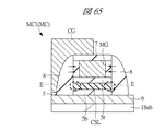
まず、その問題を図63〜図65により説明する。図63は、メモリゲート電極MGの形成工程後の基板1Subの要部断面図を示している。この工程では、通常、低抵抗ポリシリコン等からなるメモリゲート電極MGをドライエッチング法で形成した後、電荷蓄積層CSLをウエットエッチングで選択的にエッチングして形成している。ここでは、メモリゲート電極MGの幅方向(基板1Subの主面に沿う方向、短方向)端部と、電荷蓄積層CSLの幅方向端部とが一致またはほぼ一致するような状態でエッチングが行われている。しかし、このような状態でその後の酸化工程を経ると、図64および図65に示すように、メモリゲート電極MGの幅方向両端部が酸化されてしまう(図65の矢印参照)一方で電荷蓄積層CSLは窒化シリコンからなるので酸化されず残される結果、メモリゲート電極MGの実質的な幅(短方向寸法)が電荷蓄積層CSLの幅よりも短くなり、電荷蓄積層CSLの幅方向両端部がメモリゲート電極MGの幅方向外側にはみ出したような形になる。このような電荷蓄積層CSLの両端のはみ出し部分Eは、メモリゲート電極MGからの物理的な距離が遠くなるので、メモリゲート電極MGからの電界の影響を受け難くなる。このため、メモリセルMCの消去動作の際、電荷蓄積層CSLの両端のはみ出し部分Eに蓄積された電荷を引き抜き難くなる、という問題が生じる。この問題は、メモリセルMCの消去動作に際して、電荷蓄積層CSLの電荷を引き抜く方向によらない。すなわち、本実施の形態においてはメモリゲート電極MGに電子を引き抜くことで消去動作を行なっているが、基板1Subに電子を引き抜くようなメモリセルにおいても同様の問題が発生する。なお、この問題は、前記図4および図5のメモリセルでも生じる。
【0101】
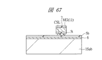
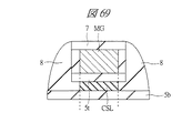
そこで、本実施の形態8では、上記電荷蓄積層をオーバーエッチングして上部のメモリゲート電極よりも小さくする工程を有するものである。これにより、最終的にメモリゲート電極の外側に電荷蓄積層の一部がはみ出さないようにすることができる。すなわち、データの消去(電荷の引き抜き)が難しくなるような部分が電荷蓄積層に形成されないようにすることができる。したがって、スプリットゲート電極型のメモリセルの動作速度(データの消去速度)を向上させることができる。また、消去動作不良の発生率を低減できるので、半導体装置の歩留りを向上させることができる。この具体例を図66〜図70の半導体装置の製造工程中におけるメモリ領域の基板1Subの要部断面図により説明する。
【0102】
まず、メモリセルのメモリゲート電極の形成工程では、電荷蓄積層(窒化シリコン)とメモリゲート電極(ポリシリコン)とを同時にエッチングするのが難しいので、2段階でエッチング処理を行う。すなわち、前記実施の形態1の図8および図9で説明した工程を経た後、図66に示すように、レジストパターンPR9をエッチングマスクとしたドライエッチング法により、メモリゲート電極MGおよび絶縁膜5tをパターニングする。この時は、ポリシリコンと窒化シリコンとのエッチング選択比を大きくとり、ポリシリコンの方がエッチングされ易い条件でエッチング処理を行う。
【0103】
続いて、レジストパターンPR9を除去した後、基板1Subに対して熱りん酸等を用いたウエットエッチング処理を施すことにより、図67に示すように、電荷蓄積層CSLを選択的にエッチングする。この時、本実施の形態8では、電荷蓄積層CSLの幅方向両端の露出側面が、メモリゲート電極MGの幅方向両端の露出側面よりも内側に位置するようにオーバーエッチング処理を施す。これにより、その後の酸化処理工程でメモリゲート電極MGの幅方向両端の側面部分が酸化されることに起因して電荷蓄積層CSLの幅方向両端部の側面がメモリゲート電極の幅方向両端の側面の外側に位置してしまうような不具合を防止することができる。このような電荷蓄積層CSLのサイドエッチング量(アンダーカット量またはオーバーエッチング量)は、熱りん酸によるウエットエッチング時間を調節ことで変えることができる。
【0104】
その後、前記実施の形態1で説明したのと同様の工程を経て、図68および図69に示すように、スプリットゲート型のメモリセルMC1を形成する。図69は、図68の要部拡大断面図を示している。本実施の形態8の場合も、図68および図69に示すように、電荷蓄積層CSLのパターニング後の酸化処理によりメモリゲート電極MGの側面部分が酸化され、メモリゲート電極MGの幅方向寸法が設計値より若干小さくなっている。上記のように本実施の形態8では、メモリゲート電極MGが酸化により小さくなってしまうのを見越して電荷蓄積層CSLの幅方向寸法を小さくしてあるので、最終的に、電荷蓄積層CSLの幅方向両端部の側面が、メモリゲート電極MGの幅方向両端部の側面とほぼ一致しており、メモリゲート電極MGの外側に、はみ出さないようにされている。このため、スプリットゲート型のメモリセルMC1の消去動作に際して、電荷の引き抜き難い箇所が電荷蓄積層CSLに存在しないので、データの消去速度を向上させることができる。また、電荷の引き抜き難い箇所が電荷蓄積層CSLに存在しないので、消去動作不良の発生率を低減でき、半導体装置の歩留りを向上させることができる。
【0105】
以上の説明では、最終的に電荷蓄積層CSLの幅方向両端部が、メモリゲート電極MGの幅方向両端部とほぼ一致している場合について説明したが、本実施の形態8は、電荷蓄積層CSLがメモリゲート電極MGの外側にはみ出していなければ良く、図70のメモリセルの要部拡大断面図に示すように、最終的に電荷蓄積層CSLの幅がメモリゲート電極MGの幅よりも小さく、電荷蓄積層CSLの幅方向両端部が、メモリゲート電極MGの幅方向両端部よりも内側に位置している構造を排除するものではない。この構造の場合は、電荷蓄積層CSLの平面全域が、メモリゲート電極MGの平面全域に内包されるようになる。このため、消去時の電荷の引き抜きの確実性を向上させることができる。
【0106】
(実施の形態9)
本実施の形態9は、前記実施の形態8の変形例であって、前記図4のスプリットゲート電極型のメモリセルMC2の形成方法に前記実施の形態8の方法を適用した場合の一例を説明する。
【0107】
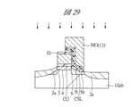
まず、前記図23〜図25で説明した工程を経た後、図71に示すように、コントロール電極CGをマスクとして自己整合的にn型の半導体領域6を基板1Subに形成する。続いて、絶縁膜5b、電荷蓄積層CSL、絶縁膜5tおよび導体膜11をCVD法等により下層から順に基板1Sub上に堆積した後、その上に、メモリゲート電極形成用のレジストパターンPR10をリソグラフィ技術により形成する。その後、そのレジストパターンPR10をエッチングマスクとして、そこから露出する導体膜11および絶縁膜5tを前記実施の形態8と同様にエッチングした後、レジストパターンPR10を除去し、図72に示すように、メモリゲート電極MGおよび絶縁膜5tをパターニングする。
【0108】
次いで、前記実施の形態8と同様に、電荷蓄積層CSLをウエットエッチング処理により選択的にエッチングすることにより、図73に示すように、電荷蓄積層CSLをパターニングする。この時、本実施の形態9でも、電荷蓄積層CSLの露出両側面が、メモリゲート電極MGの露出側面よりも内側に位置するようにオーバーエッチング処理を施す。これにより、電荷蓄積層CSLの幅方向両端部の側面がメモリゲート電極MGの幅方向両端部の側面の外側に位置してしまうような不具合を前記実施の形態8と同様に防止することができる。
【0109】
その後、前記実施の形態3で説明したのと同様の工程を経て、図74に示すように、スプリットゲート電極型のメモリセルMC2を形成する。本実施の形態9の場合も、図74に示すように、電荷蓄積層CSLのパターニング後の酸化処理によりメモリゲート電極MGの側面部分が酸化され、メモリゲート電極MGの幅方向寸法が設計値より若干小さくなっているが、上記のように本実施の形態9でも、それを見越して電荷蓄積層CSLの幅方向寸法を小さくしてあるので、最終的に、電荷蓄積層CSLの幅方向両端部の側面が、メモリゲート電極MGの幅方向両端部の側面とほぼ一致しており、メモリゲート電極MGの外側に、はみ出さないようにされている。これにより、スプリットゲート型のメモリセルMC2の消去動作に際して、前記実施の形態8と同様にデータの消去速度を向上させることができる。また、消去動作不良の発生率を低減でき、半導体装置の歩留りを向上させることができる。もちろん本実施の形態9でも図70で説明したように最終的に電荷蓄積層CSLの両端部が、メモリゲート電極MGの両端部よりも内側に位置するようにしても良い。
【0110】
(実施の形態10)
本実施の形態10は、前記実施の形態8の変形例であって、前記図5のスプリットゲート電極型のメモリセルMC3の形成方法に前記実施の形態8の方法を適用した場合の一例を説明する。
【0111】
まず、前記実施の形態9と同様に前記図71の導体膜11の堆積工程までを経た後、その導体膜11を異方性のドライエッチング処理によりエッチバックすることにより、図75に示すように、コントロールゲート電極CGの側面側に、導体膜11のサイドウォール11aを形成する。続いて、図76に示すように、基板1Subの主面上に、メモリゲート電極MG形成用のレジストパターンPR11をリソグラフィ技術により形成する。その後、そのレジストパターンPR11をエッチングマスクとして、そこから露出する導体膜11aおよび絶縁膜5tを前記実施の形態8,9と同様にエッチングしてメモリゲート電極MG(11a)および絶縁膜5tをパターニングする。
【0112】
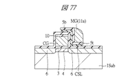
次いで、レジストパターンPR11を除去した後、前記実施の形態8,9と同様に、電荷蓄積層CSLをウエットエッチング処理により選択的にエッチングすることにより、図77に示すように、電荷蓄積層CSLをパターニングする。この時、本実施の形態10では、電荷蓄積層CSLの露出両側面が、絶縁膜5tの下に入り込み窪むようにオーバーエッチング処理を施す。これにより、電荷蓄積層CSLの幅方向片端部の側面がメモリゲート電極MGの幅方向片端部の側面の外側に位置してしまうような不具合を前記実施の形態8,9と同様に防止することができる。
【0113】
その後、前記実施の形態3で説明したのと同様の工程を経て、図78に示すように、スプリットゲート型のメモリセルMC3を形成する。本実施の形態10の場合も、図78に示すように、電荷蓄積層CSLのパターニング後の酸化処理によりメモリゲート電極MGの表面部分が酸化され、メモリゲート電極MGの幅方向寸法が設計値より若干小さくなっているが、上記のように本実施の形態10でも、それを見越して電荷蓄積層CSLの幅方向寸法を小さくしてあるので、最終的に、電荷蓄積層CSLの幅方向片端部の側面が、メモリゲート電極MGの幅方向片端部の側面とほぼ一致しており、メモリゲート電極MGの外側に、はみ出さないようにされている。これにより、スプリットゲート型のメモリセルMC3の消去動作に際して、前記実施の形態8,9と同様にデータの消去速度を向上させることができる。また、消去動作不良の発生率を低減でき、半導体装置の歩留りを向上させることができる。もちろん本実施の形態10でも図70で説明したように最終的に電荷蓄積層CSLの片端部の側面が、メモリゲート電極MGの片端部の側面よりも内側に位置するようにしても良い。
【0114】
(実施の形態11)
本実施の形態11は、前記スプリットゲート型のメモリセルについて本発明者が初めて見出した他の問題を解決するための一例を説明するものである。その問題は、メモリゲート電極の不純物濃度が高いとデータの消去時間が遅くなる、という問題である。
【0115】
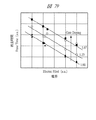
図79は、スプリットゲート電極型のメモリセルの消去特性がメモリゲート電極の不純物濃度にどのように依存するかを示している。メモリゲート電極材料は、例えばn型の低抵抗ポリシリコンを用いた。また、データ記憶に寄与する電荷は電子とされている。図79中の矢印で示すように、メモリゲート電極への不純物イオンの打ち込み濃度を増加していくと、消去速度が遅くなることが分かる。これは、メモリゲート電極側にデータ記憶に寄与する電子を引き抜く消去方式の場合、電子の引き抜きによる効果と、メモリゲート電極側から注入された正孔との再結合による効果との両方が消去動作に影響を与えているためと想定される。図80にエネルギーバンド図を例示する。白丸が正孔、黒丸が電子を示している。消去速度が変わるのは、メモリゲート電極MGから注入される正孔が電荷蓄積層CSLから引き抜かれた電子と再結合して電子・正孔対を生成したり、電荷蓄積層CSL中の電子がメモリゲート電極MGの近傍の絶縁膜5t中の欠陥準位を介してメモリゲート電極MG側に流れたり(トンネル現象)すること等に起因すると考えられる。したがって、メモリゲート電極MGの絶縁膜5tとの界面を空乏化させることにより消去速度を制御することが可能である。
【0116】
具体例として前記実施の形態1〜10のメモリセルMCのメモリゲート電極MGをn型のポリシリコンで形成し、そのメモリゲート電極MG中のn型の不純物の濃度を下げる。または、前記実施の形態1〜10のメモリセルMCのメモリゲート電極MGをn型のポリシリコンで形成し、メモリゲート電極MGの絶縁膜5tとの界面領域の不純物濃度を、同じメモリゲート電極MGの他の領域の不純物濃度よりも低くする。すなわち、同じメモリゲート電極MG中に意図的に不純物濃度差が形成されており、そのメモリゲート電極MGの電荷蓄積層CSL側の一領域(第1領域)の不純物濃度がそれ以外の領域(第2領域)に比較して相対的に低くなっている。このような構成にすることにより、電荷蓄積層CSL中の電子の引き抜きと、メモリゲート電極MG側からの正孔の注入が生じてデータ記憶に寄与する電子と再結合することとの両方の作用によりデータ消去が進められるので、消去速度を速くすることが可能となる。また、この場合も消去動作不良の発生率を低減できるので、半導体装置の歩留りを向上させることができる。
【0117】
本発明者の検討によれば、メモリゲート電極MGの全体または上記絶縁膜5tとの界面領域のn型不純物の濃度は、例えば1×10¹⁸/cm3〜2×1020/cm3程度、好ましくは8×1019/cm3〜1.5×1020/cm3程度とされている。この下限値より低いと空乏化したり、メモリゲート電極MGの抵抗値が増えたりして、消去を含めた他の動作上の問題が生じるためであり、上記上限値よりも高いと上記消去動作上の問題が生じるからである。
【0118】
また、本発明者が検討した一般的なスプリットゲート電極型のMONOS構造のメモリセルでは、そのメモリゲート電極を、周辺回路等を構成する他のMISのゲート電極と同工程で形成しているので、そのメモリゲート電極中に含まれるn型不純物の濃度が、例えば2.5×1020/cm3以上であり本実施の形態11よりも高くなっている。これに対して、本実施の形態11では、メモリゲート電極MGと上記他のMISのゲート電極とを別々に形成する。そして、メモリゲート電極MGの不純物濃度を上記のように低くする。具体的にはメモリゲート電極MGとなる相対的に低濃度のn型の不純物が導入された多結晶シリコン膜と、上記他のMISのゲート電極となる相対的に高濃度のn型の不純物が導入された多結晶シリコン膜とを別々にCVD法によって形成し、その後、パターニングすることで形成する。もちろん、メモリゲート電極MGと同一基板上の上記他のMISのゲート電極とを同時にパターニングし、後ほどの工程でイオン注入法等により他のMISのゲート電極側にn型不純物を導入し、その他のMISのゲート電極中のn型不純物の濃度を相対的に高くするようにしても良い。このイオン注入法による形成法の方が、上述の別々にCVD法で形成するよりも、上記他のMISのゲート電極の不純物濃度の制御が容易であるというメリットがある。いずれにしても、本実施の形態11では、メモリセルMCのメモリゲート電極MGのn型不純物の濃度と、同一基板上に形成された上記他のMISのゲート電極のn型不純物の濃度とが意図的に異なっており、メモリゲート電極MGのn型不純物の濃度の方が、上記他のMISのゲート電極のn型不純物の濃度よりも意図的に低くなっている。
【0119】
また、同様の考えから、前記実施の形態1〜10のメモリセルMCのメモリゲート電極MGをp型にすることにより、上記と同様の作用により消去速度を速くすることが可能となる。本発明者の検討によれば、メモリゲート電極MGをp型とした場合、メモリゲート電極MGのp型不純物の濃度は、例えば1×10¹⁸/cm3程度以上とすることが好ましい。したがって、この場合も同一基板に形成された他のMISにp型のゲート電極を持つMISがある場合に、メモリセルMCのメモリゲート電極MG中のp型不純物の濃度の方が、上記他のMISのp型のゲート電極中のp型不純物の濃度よりも意図的に高くなるような場合もある。
【0120】
(実施の形態12)
本実施の形態12では、前記実施の形態11で説明した、同じメモリゲート電極MG中に意図的に不純物濃度差が形成されており、そのメモリゲート電極MGの電荷蓄積層CSL側の一領域の不純物濃度が相対的に低くなっている場合を説明する。
【0121】
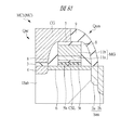
図81は、本実施の形態12のメモリセルMC1の要部断面図の一例を示している。ここでは、メモリゲート電極MGが、導体層11a,11bの積層構成を有している。導体層11a,11bはいずれもn型の低抵抗ポリシリコンからなるが、その不純物濃度が意図的に異なっており、下層側、すなわち、絶縁膜5tに接する側の導体層(第1領域)11aのn型不純物の濃度の方が、その上の導体層(第2領域)11bのn型不純物の濃度よりも低くなっている。これにより、前記実施の形態11と同様に消去速度を速くすることができる。また、半導体装置の歩留りを向上させることができる。さらに、本実施の形態12によれば、前記実施の形態11ではメモリゲート電極MG全体が低濃度のn型不純物からなる導電膜で構成されている場合も例示したが、メモリゲート電極MGに不純物濃度の高い導体層11bが設けられているので、メモリゲート電極MGの抵抗や配線との接触抵抗を低減できる。
【0122】
このような導体層11a,11bを形成するには、例えば次の第1、第2の方法を挙げることができる。第1の方法は、導体膜11a,11bをCVD法により別々に堆積する方法である。すなわち、図9等で説明した導体膜11の堆積工程の時に、導体膜11a,11bを下層から順に堆積する。この時、導体膜11a,11b中の各々のn型不純物の濃度を調節する。その後、導体膜11b上に絶縁膜7を堆積後、その積層膜を前記と同様にパターニングすることにより、メモリゲート電極MGを形成する。第2の方法は、イオン注入法により不純物濃度分布を形成する方法である。すなわち、図9等で説明したように導体膜11を堆積した後、その導体膜11にイオン注入法等によりn型不純物を導入する際に、そのイオン打ち込みエネルギーおよびドーズ量等の条件を変えて導入することにより、導体膜11中にn型不純物濃度の異なる導体層11a,11bを形成する。その後、導体膜11上に絶縁膜7を堆積後、その積層膜を前記と同様にパターニングすることにより、メモリゲート電極MGを形成する。このイオン注入法を採用した場合、各々の導体層11a,11bの不純物濃度や形成位置を制御し易いので、導体層11a,11bを、より狙いに近い状態で形成することができる。
【0123】
本実施の形態12も導体層11a,11bをp型の低抵抗ポリシリコンで形成しても良い。この場合、絶縁膜5tに接する下層側の導体膜11aのp型不純物の濃度の方が、上層側の導体膜11bのp型不純物の濃度よりも高くされている。
【0124】
(実施の形態13)
本実施の形態13では、前記実施の形態12の変形例を説明する。
【0125】
図82は、本実施の形態13のメモリセルMC1の要部断面図の一例を示している。ここでは、メモリゲート電極MGが、導体層11a,11b,11cの3層の積層構成を有している。導体層11a,11b,11cはいずれもn型の低抵抗ポリシリコンからなるが、その不純物濃度が意図的に異なっており、最下層(すなわち、絶縁膜5tに接する側)の導体層(第1領域)11aと、最上層の導体層11cのn型不純物の濃度の方が、中間の導体層(第2領域)11bのn型不純物の濃度よりも低くなっている。導体膜11a,11cのn型不純物の濃度は同じでも異なっていても良い。これにより、前記実施の形態11,12と同様に消去速度を速くすることができる。また、半導体装置の歩留りを向上させることができる。
【0126】
最上の導体層11cの濃度を低減した理由は、最上に高濃度のポリシリコン層が存在すると、洗浄処理後に高濃度のポリシリコン層の表面にウォーターマークが残ったり、高濃度のポリシリコン層に異常酸化が生じたりする場合があるので、それを回避するためである。すなわち、本実施の形態13によれば、最上の導体層11cの不純物濃度を低くしたことにより、半導体装置の製造工程中の不具合を回避できるので、半導体装置の信頼性および歩留りを向上させることができる。
【0127】
上記導体層11a,11b,11cの形成方法は、前記実施の形態12と同じなので説明を省略する。
【0128】
本実施の形態13も導体層11a,11b,11cをp型の低抵抗ポリシリコンで形成しても良い。この場合、絶縁膜5tに接する下層側の導体膜11aのp型不純物の濃度の方が、上層側の導体膜11b,11cのp型不純物の濃度よりも高くされている。
【0129】
(実施の形態14)
本実施の形態14では、前記実施の形態12の変形例を説明する。
【0130】
図83は、本実施の形態14のメモリセルMC1の要部断面図の一例を示している。ここでは、メモリゲート電極MGが、導体層11とシリサイド層14との積層構成を有している。導体膜11は、例えばn型の低抵抗ポリシリコンからなり、そのn型不純物の濃度が前記実施の形態11,12で説明したように低くされている。シリサイド層14は、例えばコバルトシリサイドまたはタングステンシリサイド等からなる。このように、導体膜11中のn型不純物の濃度を前記実施の形態11,12で記載したように低くしたとしても、導体膜11上に低抵抗なシリサイド層14を設けることにより、メモリゲート電極MGの総抵抗を低く抑えることができる。ただし、本実施の形態14でも、導体膜11をp型のポリシリコンで形成し、その上にシリサイド層14を設ける構造としても良い。
【0131】
(実施の形態15)
本実施の形態15では、前記実施の形態12のさらに他の変形例を説明する。
【0132】
図84は、本実施の形態15のメモリセルMC1の要部断面図の一例を示している。ここでは、メモリゲート電極MGが、導体層11と、バリアメタル層28と、メタル層29との3層の積層構成を有している。導体膜11は、例えばn型の低抵抗ポリシリコンからなり、そのn型不純物の濃度が前記実施の形態11,12で説明したように低くされている。バリアメタル層28は、例えば窒化タングステン(WN)等からなる。また、メタル層29は、例えばタングステン等からなる。このように、導体膜11中のn型不純物の濃度を前記実施の形態11,12で記載したように低くしたとしても、導体膜11上に低抵抗なメタル層29を設けることにより、メモリゲート電極MGの総抵抗を大幅に低くすることができる。ただし、本実施の形態15でも、導体膜11をp型のポリシリコンで形成し、その上にバリアメタル層28を介してメタル層29を設ける構造としても良い。
【0133】
(実施の形態16)
本実施の形態16は、前記スプリットゲート電極型のメモリセルについて本発明者が初めて見出したさらに他の問題を解決するための一例を説明するものである。その問題は、メモリセルのドレイン電流の劣化が生じ易い、という問題である。
【0134】
電荷蓄積層CSLまたは絶縁膜5tの材料として特に酸窒化シリコン(SiON)を使用するMONOS構造のメモリセルでは、消去動作により界面準位が形成された書き換え動作を行うとメモリセルのドレイン電流Idsが低下する場合がある。このため、メモリセルがオン状態となる時の電流劣化を考慮してメモリセルを設計する必要がある。
【0135】
すなわち、本実施の形態16では、電荷蓄積層に蓄えられた電荷をメモリゲート電極側に引き抜く動作によりデータの消去を行うスプリットゲート電極型のメモリセルにおいて、書き込みレベルの最も少ない状態が、メモリセルの初期しきい値電圧Vthよりも高い状態となるようにする。これにより、データの書込および消去に伴うドレイン電流の劣化を許容できる。したがって、メモリセルのデータの書き換え補償回数を向上でき、メモリセルの寿命を向上させることが可能となる。
【0136】
本実施の形態16のメモリセルの構造(読み出し、書き込みおよび消去動作を含む)は、前記実施の形態1〜15で説明したのと同じである。図85は、本実施の形態16のメモリセルの書き込みおよび消去状態を示している。初期状態Inは、しきい値電圧Vthが低い状態であるが、一度書き込んだ後の消去状態を初期状態Inと同じ状態にせず、それよりも高い状態とする。多値記憶の場合には、最も書き込みレベルの低い状態が、初期状態Inよりも高い状態とする方式である。この方式の場合、書き換え等の劣化によりドレイン電流Idsが減少した場合でも、深く消し込む余裕があるために、半導体装置の動作上の劣化が見えない状態とすることができる。
【0137】
以上、本発明者によってなされた発明を実施の形態に基づき具体的に説明したが、本発明は前記実施の形態に限定されるものではなく、その要旨を逸脱しない範囲で種々変更可能であることはいうまでもない。
【0138】
例えば前記実施の形態1〜16では、MONOS構造のメモリセルに適用した場合について説明したが、例えば基板上に、酸化シリコン膜、電荷蓄積用の窒化シリコン膜(または酸窒化シリコン膜)および低抵抗ポリシリコン膜(または上記と同様のポリサイドやポリメタル構造の膜)を下層から順に積層した構成を有する、MNOS(Metal Nitride Oxide Semiconductor)構造のメモリセルに適用することもできる。
【0139】
また、前記実施の形態1〜10は、消去動作に際してデータ記憶に寄与する電荷をメモリゲート電極に引き抜くメモリセル構造とした場合について説明したが、これに限定されるものではなく、消去動作に際してデータ記憶に寄与する電荷を基板側に引き抜くメモリセル構造のものにも適用できる。
【0140】
また、前記実施の形態1〜16では、電荷蓄積層を窒化膜で形成した場合について説明したが、これに限定されるものではなく、例えば酸化シリコン膜中にドット状に形成された複数のナノ結晶を有する構成としても良い。上記ナノ結晶は、一般的な不揮発性メモリの浮遊ゲート電極と同様に、データに寄与する電荷が捕獲される部分である。各ナノ結晶は、例えばCVD法により形成されている。各ナノ結晶は、物理的に離れた状態で形成されている(すなわち、離散的なトラップ準位を有する)ので、データの保持時にリークパスがあっても一部の電荷しか失われず、データ保持特性に優れている。また、データの消去および書き込み時においても、特性が多くのナノ結晶間で平均化されるので、ナノ結晶の直径や絶縁膜などの構造ばらつき、あるいは確率的振る舞いの影響を受け難いため、このメモリセルを有する半導体装置の歩留まりを向上させることができる。
【0141】
また、前記実施の形態1〜16の各々を、他の実施の形態の一つまたは2つ以上の複数個と組み合わせてもよいのは勿論である。
【0142】
以上の説明では主として本発明者によってなされた発明をその背景となった利用分野であるICカードに適用した場合について説明したが、それに限定されるものではなく、例えば携帯電話等のような移動体通信機器やパーソナルコンピュータ等のような情報処理装置に内蔵されるメモリにも適用できる。
【0143】
【発明の効果】
本願によって開示される発明のうち、代表的なものによって得られる効果を簡単に説明すれば、以下の通りである。
【0144】
すなわち、互いに隣接するように配置された第1、第2電界効果トランジスタを持つ不揮発性メモリセルを半導体基板に有する半導体装置の電気的特性を向上させることができる。
【図面の簡単な説明】
【図1】本発明の一実施の形態である半導体装置のメモリセルの回路図である。
【図2】図1のメモリセルのデバイス基本構造例の要部断面図である。
【図3】図1および図2のメモリセルのデータの読み出し動作、消去動作および書き込み動作時の各部への印加電圧値の一例の説明図である。
【図4】図1のメモリセルのデバイス基本構造の他の例の要部断面図である。
【図5】図1のメモリセルのデバイス基本構造のさらに他の例の要部断面図である。
【図6】図1のメモリセルの形成工程で生じる不具合を説明するための半導体装置の製造工程中の要部断面図である。
【図7】図1のメモリセルの形成工程で生じる不具合を説明するための半導体装置の製造工程中の要部断面図である。
【図8】本発明の一実施の形態である半導体装置の製造工程中の要部断面図である。
【図9】図8に続く半導体装置の製造工程中の要部断面図である。
【図10】図9に続く半導体装置の製造工程中の要部断面図である。
【図11】図10に続く半導体装置の製造工程中の要部断面図である。
【図12】図11に続く半導体装置の製造工程中の要部断面図である。
【図13】図12に続く半導体装置の製造工程中の要部断面図である。
【図14】図13に続く半導体装置の製造工程中の要部断面図である。
【図15】図14に続く半導体装置の製造工程中の要部断面図である。
【図16】図15に続く半導体装置の製造工程中の要部断面図である。
【図17】図16に続く半導体装置の製造工程中の要部断面図である。
【図18】図17に続く半導体装置の製造工程中の要部断面図である。
【図19】図18に続く半導体装置の製造工程中の要部断面図である。
【図20】本発明の他の実施の形態である半導体装置の製造工程中の要部断面図である。
【図21】図20に続く半導体装置の製造工程中の要部断面図である。
【図22】図21に続く半導体装置の製造工程中の要部断面図である。
【図23】本発明の他の実施の形態である半導体装置の製造工程中の要部断面図である。
【図24】図23に続く半導体装置の製造工程中の要部断面図である。
【図25】図24に続く半導体装置の製造工程中の要部断面図である。
【図26】図25に続く半導体装置の製造工程中の要部断面図である。
【図27】図26に続く半導体装置の製造工程中の要部断面図である。
【図28】図27に続く半導体装置の製造工程中の要部断面図である。
【図29】図28に続く半導体装置の製造工程中の要部断面図である。
【図30】図29に続く半導体装置の製造工程中の要部断面図である。
【図31】図30に続く半導体装置の製造工程中の要部断面図である。
【図32】図1のメモリセルの形成工程で生じる他の不具合を説明するための半導体装置の製造工程中の要部断面図である。
【図33】図32の領域Bの拡大断面図である。
【図34】本発明の他の実施の形態である半導体装置の製造工程中の要部断面図である。
【図35】図34に続く半導体装置の製造工程中の要部断面図である。
【図36】図35に続く半導体装置の製造工程中の要部断面図である。
【図37】図36に続く半導体装置の製造工程中の要部断面図である。
【図38】図37に続く半導体装置の製造工程中の要部断面図である。
【図39】図38の領域Dの拡大断面図である。
【図40】本発明の他の実施の形態である半導体装置の要部拡大断面図である。
【図41】図1のメモリセルの形成工程で生じる他の不具合を説明するための半導体装置の製造工程中の要部断面図である。
【図42】図41に続く半導体装置の製造工程中の要部断面図である。
【図43】図42に続く半導体装置の製造工程中の要部断面図である。
【図44】本発明の他の実施の形態である半導体装置の製造工程中の要部断面図である。
【図45】図44に続く半導体装置の製造工程中の要部断面図である。
【図46】図45に続く半導体装置の製造工程中の要部断面図である。
【図47】図46に続く半導体装置の製造工程中の要部断面図である。
【図48】図47に続く半導体装置の製造工程中の要部断面図である。
【図49】図48に続く半導体装置の製造工程中の要部断面図である。
【図50】図49に続く半導体装置の製造工程中の要部断面図である。
【図51】図50に続く半導体装置の製造工程中の要部断面図である。
【図52】図51に続く半導体装置の製造工程中の要部断面図である。
【図53】本発明の他の実施の形態である半導体装置の製造工程中の要部断面図である。
【図54】図53に続く半導体装置の製造工程中の要部断面図である。
【図55】図54に続く半導体装置の製造工程中の要部断面図である。
【図56】図55に続く半導体装置の製造工程中の要部断面図である。
【図57】図56に続く半導体装置の製造工程中の要部断面図である。
【図58】図57に続く半導体装置の製造工程中の要部断面図である。
【図59】図58に続く半導体装置の製造工程中の要部断面図である。
【図60】図59に続く半導体装置の製造工程中の要部断面図である。
【図61】図60に続く半導体装置の製造工程中の要部断面図である。
【図62】本発明の他の実施の形態である半導体装置のメモリ領域の一例の要部平面図である。
【図63】図1のメモリセルの形成工程で生じる他の不具合を説明するための半導体装置の製造工程中の要部断面図である。
【図64】図63に続く半導体装置の製造工程中の要部断面図である。
【図65】図64の要部拡大断面図である。
【図66】本発明の他の実施の形態である半導体装置の製造工程中の要部断面図である。
【図67】図66に続く半導体装置の製造工程中の要部断面図である。
【図68】図67に続く半導体装置の製造工程中の要部断面図である。
【図69】図68の半導体装置のメモリセルの要部拡大断面図である。
【図70】本発明の他の実施の形態である半導体装置のメモリセルの要部拡大断面図である。
【図71】本発明の他の実施の形態である半導体装置の製造工程中の要部断面図である。
【図72】図71に続く半導体装置の製造工程中の要部断面図である。
【図73】図72に続く半導体装置の製造工程中の要部断面図である。
【図74】図73に続く半導体装置の製造工程中の要部断面図である。
【図75】本発明の他の実施の形態である半導体装置の製造工程中の要部断面図である。
【図76】図75に続く半導体装置の製造工程中の要部断面図である。
【図77】図76に続く半導体装置の製造工程中の要部断面図である。
【図78】図77に続く半導体装置の製造工程中の要部断面図である。
【図79】図1のメモリセルの形成工程で生じる他の不具合を説明するための図であり、消去動作のメモリゲート電極中の不純物濃度依存性を示すグラフ図である。
【図80】メモリゲート電極およびその近傍の電荷蓄積層のエネルギーバンド図である。
【図81】本発明の他の実施の形態である半導体装置の要部断面図である。
【図82】本発明の他の実施の形態である半導体装置の要部断面図である。
【図83】本発明の他の実施の形態である半導体装置の要部断面図である。
【図84】本発明の他の実施の形態である半導体装置の要部断面図である。
【図85】本発明のさらに他の実施の形態である半導体装置の書き込みおよび消去状態の説明図である。
【符号の説明】
1Sub 半導体基板
2a 半導体領域
2b 半導体領域
3 ゲート絶縁膜
4 半導体領域
5b,5t 絶縁膜
6 半導体領域
7 絶縁膜
8 サイドウォール
9 サイドウォール
10 絶縁膜
11 導体膜
11a 導体層
11b 導体層
13 窪み
14 シリサイド層
15 絶縁膜
17 導体膜
19 絶縁膜
21 導体膜
21a 導体膜
23 絶縁膜
23a,23b 絶縁膜
25 分離部
28 バリアメタル層
29 メタル層
MC,MC1〜MC3 メモリセル
D ドレイン電極
Drm ドレイン領域
S ソース電極
Srm ソース領域
CG コントロールゲート電極
MG メモリゲート電極
CSL 電荷蓄積層
Qnc nチャネル型のMIS・FET
Qnm nチャネル型のMIS・FET
PR1〜PR11 フォトレジストパターン
CNT コンタクトホール
PLG プラグ
M1 第1層配線
HG ゲート電極[0001]
TECHNICAL FIELD OF THE INVENTION
The present invention relates to a method of manufacturing a semiconductor device and a semiconductor device technology, and more particularly to a method of manufacturing a semiconductor device having a non-volatile memory and a technology effective when applied to the semiconductor device.
[0002]
[Prior art]
An electrically rewritable non-volatile memory such as an EEPROM (Electrically Erasable Programmable Read Only Memory) or a flash memory allows a program to be rewritten on-board, thereby shortening the development period and improving the development efficiency. In addition, applications are expanding to a variety of applications, such as support for low-volume, high-mix production, tuning by destination, and program updates after shipment. In particular, in recent years, there is a great need for a microcomputer having an MPU (Micro Processing Unit) and an EEPROM (or flash memory). As electrically rewritable nonvolatile memories, EEPROMs using ordinary polysilicon as floating electrodes are mainly used. However, in the EEPROM of this structure, if any part of the oxide film surrounding the floating gate electrode has a defect, the charge storage layer is a conductor, so that all the charges stored in the storage node due to abnormal leakage are removed. May be lost. In particular, it is considered that this problem will become more remarkable as miniaturization progresses and the degree of integration increases.
[0003]
Therefore, in recent years, nitride films (Si 3 N 4 , Etc.) have attracted attention. The MNOS (Metal Nitride Oxide Semiconductor) structure or the MONOS (Metal Oxide Nitride Oxide Semiconductor) structure having a charge storage layer. In this case, the electric charge contributing to data storage is accumulated in the discrete trap of the nitride film, which is an insulator, so that even if a defect occurs in any part of the oxide film surrounding the accumulation node and abnormal leakage occurs, the electric charge is stored. Since all the charges in the storage layer do not escape, the reliability of data retention can be improved.
[0004]
As a configuration of a memory cell, a memory cell having a single transistor structure has been proposed. As the writing / erasing method, there are writing by FN (Fowler Nordheim) tunneling injection from the semiconductor substrate, erasing by FN tunneling current to the semiconductor substrate, writing by hot electron injection, semiconductor substrate or source and drain. There has been proposed a method of performing erasing by FN tunneling current to a region. Furthermore, since the MONOS-type single transistor cell structure is more susceptible to disturbance than the EEPROM cell structure, a two-transistor split-gate memory cell structure provided with a control gate electrode has been proposed. This type of split gate type memory cell structure has a memory gate using a control gate electrode rising type, a memory gate electrode rising type, and a side wall type due to a difference in a process in which one of the gate electrodes runs on the other gate electrode. An electrode riding type or the like can be realized.
[0005]
For example, in Japanese Patent Application Laid-Open No. 6-85251, although not a memory cell, after forming a gate electrode of a MOS-FET, a surface layer portion of a semiconductor substrate located on both sides of the gate electrode is etched to form a channel region and a source. A technique for forming a step with a drain region is disclosed (for example, Patent Document 1).
[0006]
Also, for example, in Japanese Patent Application Laid-Open No. 5-267250, after a sidewall is formed on a side surface of an adjacent gate electrode (floating gate) in a manufacturing process of a flash memory, a lower layer field is formed by using the gate electrode and the sidewall as a mask. A technique for forming a groove by partially etching an insulating film and a semiconductor substrate is disclosed (for example, Patent Document 2).
[0007]
Also, for example, in Japanese Patent Application Laid-Open No. 2000-91452, during operation of a non-volatile memory having a MONOS structure, data is not written or read to or from a non-selected memory cell transistor adjacent to a selected memory cell transistor. As described above, a configuration is disclosed in which an offset sidewall is provided on a channel side surface of an insulating film pattern on a buried region for a source and a drain of a memory cell transistor so that the channel of the memory cell transistor is difficult to expand ( For example, Patent Document 3).
[0008]
For example, Japanese Patent Application Laid-Open No. H6-125094 discloses a configuration in which an offset region is provided between an ONO film and a gate electrode of a memory cell transistor and a source region (for example, Patent Document 4).
[0009]
For example, Japanese Patent Application Laid-Open No. 2001-168219 discloses a configuration in which a step is provided in a channel of a MONOS type memory cell transistor and channel hot electrons are injected through the step. Also, in paragraph number 0038 of this publication, the gate electrode of a memory cell transistor that performs erasure by extracting charges using an FN tunnel current is made conductive by introducing p-type or n-type impurities at a high concentration. (For example, Patent Document 5).
[0010]
Further, for example, Japanese Patent Application Laid-Open No. 2002-298593 discloses a method for suppressing or preventing data from being destroyed by increasing the threshold voltage of an unselected memory cell by repeating the read operation of the EEPROM. There is disclosed a configuration in which the threshold voltage of a cell is set higher than the lower one of the voltages applied to the source and drain during data reading and lower than the voltage applied to the gate electrode during data reading. (For example, Patent Document 6).
[0011]
[Patent Document 1]
JP-A-6-85251
[0012]
[Patent Document 2]
JP-A-5-267250
[0013]
[Patent Document 3]
JP 2000-91452 A
[0014]
[Patent Document 4]
JP-A-6-125094
[0015]
[Patent Document 5]
JP 2001-168219 A
[0016]
[Patent Document 6]
JP-A-2002-298591
[0017]
[Problems to be solved by the invention]
However, a nonvolatile memory employing a split gate type memory cell structure as described above and using a nitride film as a charge storage layer is a new structure. Is one of the important issues.
[0018]
An object of the present invention is to provide a technique capable of improving electrical characteristics in a semiconductor device having a nonvolatile memory using a split gate type memory cell structure and using a nitride film as a charge storage layer.
[0019]
The above and other objects and novel features of the present invention will become apparent from the description of the present specification and the accompanying drawings.
[0020]
[Means for Solving the Problems]
The following is a brief description of an outline of typical inventions disclosed in the present application.
[0021]
That is, the present invention relates to a semiconductor device having a nonvolatile memory cell having first and second field-effect transistors disposed adjacent to each other on a semiconductor substrate, wherein the first field-effect transistor already formed on the semiconductor substrate is provided. After etching a portion of the first semiconductor region of the first conductivity type of the transistor which is arranged in the formation region of the second field effect transistor, the first conductivity type of the second field effect transistor is etched in the etched region. A second semiconductor region of the second conductivity type, which is opposite to the above, is formed.
[0022]
Further, the present invention provides a semiconductor device having a nonvolatile memory cell having first and second field-effect transistors disposed adjacent to each other on a semiconductor substrate, wherein In the first conductivity type first semiconductor region, the end on the side of the second field effect transistor protrudes below the second gate electrode of the second field effect transistor or coincides with the end of the second gate electrode. And forming a second semiconductor region of a second conductivity type opposite to the first conductivity type below the second gate electrode of the second field effect transistor.
[0023]
Further, the present invention provides a nonvolatile memory cell having a gate electrode and a charge storage layer. The over-etching is performed so as to be located below the side surface of the end.
[0024]
The present invention also provides a nonvolatile memory having a structure in which one of the first and second gate electrodes of the first and second field effect transistors arranged adjacent to each other runs on the other gate electrode. In the semiconductor device having a cell, before depositing the conductor film for forming the one gate electrode, the semiconductor substrate on the side surface side of the other gate electrode, on which the one gate electrode does not ride, A protective film is formed on the main surface.
[0025]
Further, according to the present invention, there is provided a nonvolatile memory cell for erasing data by extracting a charge stored in a charge storage layer to an n-type gate electrode, wherein the charge storage in the n-type gate electrode is performed. The concentration of the n-type impurity in the first region on the layer side is lower than the concentration of the n-type impurity in the second region other than the first region in the n-type gate electrode.
[0026]
Further, the present invention provides a nonvolatile memory cell having a nonvolatile memory cell for erasing data by extracting a charge stored in a charge storage layer to a gate electrode side. In a state higher than the threshold voltage.
[0027]
BEST MODE FOR CARRYING OUT THE INVENTION
Before describing the embodiments of the present invention in detail, the meanings of terms in the present embodiment will be described as follows.
[0028]
Silicon nitride, silicon nitride or silicon nitride is referred to as Si 3 N 4 Needless to say, not only this but also an insulating film of silicon nitride having a similar composition.
[0029]
Hereinafter, embodiments of the present invention will be described in detail with reference to the drawings. In the following embodiments, when it is necessary for the sake of convenience, the description will be made by dividing into a plurality of sections or embodiments, but they are not irrelevant to each other, unless otherwise specified. Is related to some or all of the other modifications, details, supplementary explanations, and the like. Further, in the following embodiments, when referring to the number of elements (including the number, numerical value, amount, range, etc.), a case where it is particularly specified, and a case where it is clearly limited to a specific number in principle, etc. However, the number is not limited to the specific number, and may be more than or less than the specific number. Further, in the following embodiments, the constituent elements (including element steps, etc.) are not necessarily essential unless otherwise specified, and when it is deemed essential in principle. Needless to say. Similarly, in the following embodiments, when referring to the shapes, positional relationships, and the like of the constituent elements, the shapes are substantially the same unless otherwise specified and in cases where it is considered that it is not clearly apparent in principle. And the like. This is the same for the above numerical values and ranges. In all the drawings for describing the present embodiment, components having the same function are denoted by the same reference numerals, and repeated description thereof will be omitted. Further, in some drawings used in the present embodiment, hatching is used even in a plan view so as to make the drawings easy to see. In the following embodiments, a MIS • FET (Metal Insulator Field Effect Transistor) representing a field-effect transistor is abbreviated as MIS, a p-channel MIS • FET is abbreviated as pMIS, and an n-channel MIS • FET is abbreviated. FET is abbreviated as nMIS. Note that the MOS • FET (Metal Oxide Semiconductor FET) has a gate insulating film made of silicon oxide (SiO 2). 2 Etc.) It is a field-effect transistor having a structure of a film, and is included in the lower concept of the MIS.
[0030]
(Embodiment 1)
The present inventors have studied a semiconductor device having a non-volatile memory such as an EEPROM or a flash memory, and each of the plurality of memory cells of the non-volatile memory has a split gate electrode structure having a two-transistor structure, for example. And a MONOS (Metal Oxide Nitride Semiconductor) structure having a nitride film (silicon nitride film or the like) on one transistor side as a charge storage layer for data storage. In the case of the MONOS structure, the single-transistor memory cell is more susceptible to disturbance than in the case of the EEPROM structure. Therefore, in order to prevent this, a split gate electrode structure of a two-transistor structure is employed. In addition, in any of the above-described split gate type memory cell structures, holes are injected from the semiconductor substrate into the charge storage layer or electrons are extracted from the charge storage layer into the semiconductor substrate during erasing, so that a negative voltage is applied to the memory gate electrode. Since a power supply circuit is required, the memory occupancy is reduced, and the manufacturing yield is reduced. In addition, when writing is performed with the FN tunneling current, there is a problem that it is difficult to increase the writing speed. Therefore, at the time of data writing, the writing time is shortened by injecting electrons from the semiconductor substrate into the charge storage nitride film by hot electron injection, while a positive voltage is applied to the memory gate electrode side at the time of data erasing. The operation of extracting electrons in the nitride film for charge storage to the memory gate electrode side can simplify the power supply circuit. However, a memory cell structure that performs the above-described circuit operation has not been studied in detail. Therefore, in this embodiment, a case will be described in which the present invention is applied to a memory cell configuration which performs the above-described circuit operation. However, the following embodiment is applied to a memory cell structure having the above-described circuit operation. The present invention is not limited to the above, and includes those applicable to memory cells having various circuit operations.
[0031]
FIG. 1 shows a circuit diagram of the memory cell MC. The memory cell MC includes, for example, two transistors, i.e., nMISQnc for memory cell selection (hereinafter simply referred to as nMISQnc for selection) and nMISQnm for memory, between the drain electrode D and the source electrode S of the memory cell MC. have. The nMIS Qnc for selection has a control gate electrode CG, and the nMIS Qnm for memory has a memory gate electrode MG and the charge storage layer CSL. Vd denotes a drain voltage, Vcg denotes a control gate voltage, Vmg denotes a memory gate voltage, Vs denotes a source voltage, and Vsub denotes a substrate voltage.
[0032]
FIG. 2 shows an example of a basic device cross section of the memory cell MC. Here, a memory cell MC1 (MC) of a control gate electrode riding type is illustrated. The semiconductor substrate (hereinafter, simply referred to as a substrate) 1Sub is made of, for example, p-type silicon (Si) single crystal, and its main surface (device formation surface) includes nMISQnc for selecting the memory cell MC1 and nMISQnm for memory. Is arranged. The drain region Drm and the source region Srm of the memory cell MC1 are, for example, n − Semiconductor region 2a and n having a higher impurity concentration than
[0033]
The control gate electrode CG and the memory gate electrode MG are made of, for example, n-type low-resistance polysilicon. Part of the control gate electrode CG runs over the memory gate electrode MG. Between the control gate electrode CG and the main surface of the substrate 1Sub, for example, a thin silicon oxide (SiO 2 Etc.) are provided. On the main surface of the substrate 1Sub below the
[0034]
On the other hand, between the memory gate electrode MG and the main surface of the substrate 1Sub, the charge storage layer CSL is provided in a state sandwiched between upper and lower insulating
[0035]
In addition, the insulating
[0036]
As a specific implementation method, for example, oxynitridation (NO) annealing is performed after the formation of the insulating
[0037]
Further, by forming the gate insulating film (silicon oxide film) of the nMIS Qnc for selection or the MIS around the memory cell by the CVD method, the film forming temperature can be lowered as compared with the thermal oxidation step, so that the insulating
[0038]
An n-
[0039]
On the side surfaces of the memory gate electrode MG, the insulating
[0040]
In such a memory cell MC1, charges contributing to data storage are injected from the substrate 1Sub to the trap level in the charge storage layer CSL at a position indicated by an arrow A or the like by hot electron injection. Since these charges are accumulated discretely, even if a defect occurs in any part of the oxide film (insulating
[0041]
FIG. 3 shows an example of a voltage value applied to each part in the data read operation Re, the erase operation Er, and the write operation Wr of the memory cell MC in FIGS. 1 and 2.
[0042]
In the data read operation Re, for example, about 1 V is applied to the drain electrode D (drain region Drm) of the selected memory cell MC, and about 1.5 V is applied to the control gate electrode CG, for example, about 1.5 V to the source electrode S of the selected memory cell MC. For example, 0 (zero) V is applied to the source region Srm), the memory gate electrode MG, and the substrate 1Sub to turn on the nMISQnc for selecting the memory cell MC. At this time, the threshold voltage of the nMISQnm for memory changes depending on the presence or absence of electrons in the charge storage layer CSL of the nMISQnm for memory, and current flows or does not flow between the drain region Drm and the source region Srm. Therefore, the stored data is read.
[0043]
Further, in the data erasing operation Er, for example, 0 (zero) V and the control gate electrode CG are applied to the drain electrode D (drain region Drm), the source electrode S (source region Srm) and the
[0044]
Further, data writing employs a source side hot electron injection method. In the data write operation Wr, for example, 0 (zero) V is applied to the drain electrode D (drain region Drm) and the substrate 1Sub of the selected memory cell MC, and about 1.5 V is applied to the control gate electrode CG, for example, the memory gate electrode MG. Then, for example, about 12 V is applied to the source electrode S (source region Srm) of the selected memory cell MC, for example, about 6 V. Thus, hot electrons generated in the channel of the memory cell MC are injected into the charge storage layer CSL, and data is written.
[0045]
4 and 5 show another example of the basic device cross section of the memory cell MC of the split gate electrode type. FIG. 4 illustrates a memory cell MC2 (MC) of a memory gate electrode rising type, and FIG. 5 illustrates a memory cell MC3 (MC) of a sidewall type memory gate electrode rising type. In the memory cells MC2 and MC3 of FIGS. 4 and 5, a part of the memory gate electrode MG runs on the control gate electrode CG side, but the insulating
[0046]
Next, with reference to FIGS. 6 and 7, a problem first discovered by the inventor of the split gate type memory cells MC (MC1 to MC3) shown in FIGS. 2, 4 and 5 will be described.
[0047]
FIG. 6 is a sectional view of a main part of the substrate 1Sub during the step of forming the memory cell MC1 of the split gate electrode type shown in FIG. An n-
[0048]
As described above, in the split gate electrode type memory cells MC1 to MC3 of FIGS. 2, 4 and 5, since the nMISQnc for selection and the nMISQnm for memory are adjacent to each other, the channels for forming the nMISQnc and Qnm are formed. To form a semiconductor region, an impurity for forming one of the channel-forming semiconductor regions is implanted into the substrate 1Sub, and then an impurity of the opposite conductivity type is implanted so as to cancel the impurity. It is necessary to form a semiconductor region for formation. For this reason, a large amount of impurities are implanted into one of the channel forming semiconductor regions, so that the overall impurity concentration of the channel forming semiconductor region into which the large amount of impurities is implanted increases. As a result, electrical characteristics such as a decrease in carrier mobility (a decrease in drain current Ids) and an increase in variation in threshold voltage are caused.
[0049]
Therefore, in the first embodiment, in the step of forming the memory cell MC of the split gate electrode type having two MISs, the MIS for selection and the MIS for memory, the semiconductor region for channel formation of one MIS is etched. After that, a semiconductor region for channel formation of the other MIS is formed. Accordingly, the impurity concentration of the semiconductor region for channel formation of the other MIS can be reduced, so that the mobility of carriers can be improved, and the drain current Ids in the memory cell MC can be increased. Therefore, the operating speed (data reading speed) of the memory cell MC of the split gate electrode type can be improved. Further, since the variation in the threshold voltage can be reduced, the operation reliability of the split gate memory cell MC can be improved.
[0050]
This specific example will be described with reference to cross-sectional views of main parts of the substrate 1Sub in the memory area during the manufacturing process of the semiconductor device shown in FIGS. Here, an example of application to the memory cell MC1 in FIG. 2 will be described.
[0051]
First, as shown in FIG. 8, for example, arsenic (As) is ion-implanted into a main surface of a substrate 1Sub (a semiconductor wafer having a substantially circular plane in this stage) made of, for example, p-type silicon (Si) single crystal. Introduce. Thus, an n-
[0052]
Next, as shown in FIG. 9, an insulating
[0053]
Next, as shown in FIG. 12, after forming a resist pattern PR2 on the main surface of the substrate 1Sub so that the side of the nMIS formation region for selection is exposed, the resist pattern PR2, the
[0054]
Next, as shown in FIG. 13, using the resist pattern PR2, the
[0055]
Next, as shown in FIG. 14, a
[0056]
Next, an insulating film made of, for example, silicon oxide is deposited on the main surface of the substrate 1Sub by a CVD method, and then this is etched back by an anisotropic dry etching method to form a control gate as shown in FIG.
[0057]
Next, as shown in FIG. 19, an insulating
[0058]
(Embodiment 2)
In the second embodiment, which is a modification of the first embodiment, an example in which the substrate 1Sub on both sides of the memory gate electrode is etched will be described with reference to FIGS. This will be described with reference to a cross-sectional view of a main part.
[0059]
First, after the steps described in the first embodiment with reference to FIGS. 8 to 11 are performed, the same etching process as that described with reference to FIG. 12 is performed on the substrate 1Sub, so that the memory gates as shown in FIG. A
[0060]
In the second embodiment, since the
[0061]
(Embodiment 3)
The methods of the first and second embodiments can be applied to the memory cells MC2 and MC3 of FIGS. Therefore, in the third embodiment, an example in which the method of the second embodiment is applied to the memory cell MC2 of FIG. 4 will be described with reference to cross-sectional views of main parts during the manufacturing process of the semiconductor device of FIGS.
[0062]
First, as shown in FIG. 23, for example, boron difluoride (BF) is formed on the main surface of a substrate 1Sub (the semiconductor wafer) made of, for example, p-type silicon (Si) single crystal. 2 ) Is introduced by ion implantation. As a result, the p-
[0063]
Subsequently, as shown in FIG. 24, a
[0064]
Next, by performing the same etching treatment as that described with reference to FIG. 12 on the substrate 1Sub, a
[0065]
Next, as shown in FIG. 28, on the main surface of the substrate 1Sub, the insulating
[0066]
In the third embodiment, the
[0067]
(Embodiment 4)
The fourth embodiment describes an example for solving the other problems first discovered by the present inventors regarding the split gate electrode type memory cell. The problem is that the source / drain semiconductor region of the MIS for selecting a memory cell is offset with respect to the control gate electrode.
[0068]
First, the problem will be described with reference to FIGS. 32 is a cross-sectional view of a main part of the memory cell MC1, and FIG. 33 is an enlarged cross-sectional view of a region B surrounded by a broken line in FIG. In the case of the memory cell MC1, the p-
[0069]
Therefore, in the fourth embodiment, a spacer such that the end of the semiconductor region for channel formation of the MIS for selection is separated from the side surface of the sidewall formed on the side surface of the memory gate electrode of the MIS for memory is used. After forming on the side wall of the side wall of the memory gate electrode, an impurity for forming a semiconductor region for forming a channel of the MIS for selection is introduced into the substrate 1Sub. This ensures that the ends of the semiconductor region serving as the source / drain region of the MIS for selection (the semiconductor region for forming the channel of the MIS for memory) overlap under the control gate electrode. The drain current Ids of the gate type memory cell can be improved. Therefore, the operating speed (data reading speed) of the split gate memory cell can be improved. This specific example will be described with reference to cross-sectional views of main parts of the substrate 1Sub in the memory area during the manufacturing process of the semiconductor device shown in FIGS.
[0070]
First, after the steps described with reference to FIGS. 8 to 11 of the first embodiment, as shown in FIG. 34, the insulating
[0071]
Subsequently, as shown in FIG. 35, a resist pattern PR2 is formed on the main surface of the substrate 1Sub in the same manner as in the first embodiment, and then, as described in FIG. For example, boron difluoride (BF 2 ) Or boron (B) is ion-implanted to form a p-
[0072]
After removing the resist pattern PR2, the insulating
[0073]
In the fourth embodiment, as shown in FIG. 39, the end of n-
[0074]
However, in the fourth embodiment, the case where the n-
[0075]
Further, the fourth embodiment may be combined with the first and second embodiments. That is, after the
[0076]
Further, the insulating
[0077]
(Embodiment 5)
The fifth embodiment describes an example for solving another problem first found by the present inventors regarding the split gate electrode type memory cell. The problem is that in the process of patterning the gate electrode on the rising side, a part of the gate electrode on the rising side is left on the side surface of the gate electrode not on the top, and when removing it, the main surface of the substrate is removed. Is a problem of etching.
[0078]
First, the problem will be described with reference to FIGS. FIGS. 41 to 43 are cross-sectional views of main parts of the substrate 1Sub during the patterning process of the control gate electrode. As shown in FIG. 41, after a
[0079]
Therefore, the fifth embodiment includes a step of forming a protective film on the substrate on which the gate electrode does not ride. Thereby, when removing the etch residue generated during the processing of the gate electrode on the riding side, the main surface of the substrate 1Sub is protected by the protective film, so that the main surface of the substrate 1Sub can be prevented from being etched. This specific example will be described with reference to cross-sectional views of main parts of the substrate 1Sub in the memory area during the manufacturing process of the semiconductor device shown in FIGS.
[0080]
First, after going through the steps described in the first embodiment with reference to FIGS. 8 to 11, as shown in FIG. 44, a resist pattern PR2 is formed on the main surface of the substrate 1Sub (semiconductor wafer). Boron (BF) 2 ) Or boron (B) is ion-implanted to form a p-
[0081]
Next, as shown in FIG. 47, after the
[0082]
Then, after removing the resist pattern PR4, as shown in FIG. 50, an impurity such as phosphorus or arsenic is ion-implanted into the substrate 1Sub, and − The
[0083]
The fifth embodiment may be combined with the first and second embodiments. That is, after forming the
[0084]
Further, the fifth embodiment may be combined with the fourth embodiment. In this case, the insulating
[0085]
(Embodiment 6)
The sixth embodiment is a modification of the fifth embodiment, and describes an example in which the protective insulating
[0086]
53 to 61 are main-portion cross-sectional views of the substrate 1Sub during the manufacturing process of the semiconductor device of the sixth embodiment. The left side of each drawing shows a main-portion cross-sectional view of the memory region, and the right side shows peripheral circuits. Main part sectional view of a high breakdown voltage nMIS formation region for use.
[0087]
FIG. 53 is a cross-sectional view of a main part of the substrate 1Sub (semiconductor wafer) after the steps described in FIGS. 8 to 11 and the steps described in FIG. On the right side of FIG. 53, a groove-shaped
[0088]
First, by subjecting such a substrate 1Sub to an oxidation treatment, a
[0089]
Next, as shown in FIG. 57, the
[0090]
Then, after the resist pattern PR8 is removed, as shown in FIG. 60, for example, arsenic is introduced into the substrate 1Sub by an ion implantation method or the like while the insulating
[0091]
As described above, in the sixth embodiment, since the protective insulating
[0092]
In the sixth embodiment, the protective insulating film for removing the
[0093]
(Embodiment 7)
When the protective insulating film of the fifth and sixth embodiments is formed by the CVD method, the gate electrode formed first of the memory cell is covered with the protective insulating film. Layer cannot be formed.
[0094]
Therefore, in the seventh embodiment, a silicide layer is formed in a contact hole portion where a wiring such as a first-layer wiring is in contact with and connected to a gate electrode formed first. Thereby, the contact resistance between the gate electrode formed first and the wiring such as the first layer wiring can be reduced.
[0095]
FIG. 62 is a plan view of a main part of a memory area as a specific example of the seventh embodiment. A portion corresponding to a cross-sectional view taken along line X1-X1 in FIG. 62 is a cross-sectional view on the left side in FIGS. 44 to 52 of the fifth embodiment or FIGS. 53 to 61 of the sixth embodiment. On the upper surfaces of the control gate electrode CG and the memory gate electrode MG, the portions where the silicide layers 14 are formed by the salicide process are hatched. The
[0096]
In order to form such a configuration, in the steps described with reference to FIGS. 45 and 46, the pattern shape of the resist pattern PR5 of FIG. 45 is changed to the area of the memory gate electrode MG where the contact holes CNT are arranged. The protective
[0097]
As a method for forming the
[0098]
The seventh embodiment and the fifth and sixth embodiments can also be applied to the split gate type memory cell of FIGS. 4 and 5.
[0099]
(Embodiment 8)
The eighth embodiment describes an example for solving the other problem first found by the present inventors regarding the split gate electrode type memory cell. The problem is that the width (short dimension) of the charge storage layer CSL becomes larger than the width (short dimension) of the memory gate electrode, so that the erasing operation becomes difficult.
[0100]
First, the problem will be described with reference to FIGS. FIG. 63 is a cross-sectional view of a main part of the substrate 1Sub after the step of forming the memory gate electrode MG. In this step, usually, the memory gate electrode MG made of low-resistance polysilicon or the like is formed by dry etching, and then the charge storage layer CSL is selectively etched by wet etching. Here, the etching is performed in such a state that the end of the memory gate electrode MG in the width direction (the direction along the main surface of the substrate 1Sub, the short direction) coincides with or substantially coincides with the end of the charge storage layer CSL in the width direction. Has been done. However, if a subsequent oxidation process is performed in such a state, both ends in the width direction of the memory gate electrode MG are oxidized as shown in FIGS. Since the layer CSL is made of silicon nitride and is left unoxidized, the substantial width (shorter dimension) of the memory gate electrode MG becomes shorter than the width of the charge storage layer CSL, and both ends of the charge storage layer CSL in the width direction. Is protruded outside the width direction of the memory gate electrode MG. The protruding portions E at both ends of the charge storage layer CSL are far from the influence of the electric field from the memory gate electrode MG because the physical distance from the memory gate electrode MG is long. For this reason, at the time of the erasing operation of the memory cell MC, there is a problem that it is difficult to extract the charges stored in the protruding portions E at both ends of the charge storage layer CSL. This problem does not depend on the direction in which the charge of the charge storage layer CSL is extracted during the erasing operation of the memory cell MC. That is, in the present embodiment, the erasing operation is performed by extracting electrons to the memory gate electrode MG. However, a similar problem occurs in a memory cell in which electrons are extracted to the substrate 1Sub. This problem also occurs in the memory cells shown in FIGS.
[0101]
Therefore, the eighth embodiment includes a step of overetching the charge storage layer to make it smaller than the upper memory gate electrode. Thereby, it is possible to prevent a part of the charge storage layer from finally protruding outside the memory gate electrode. That is, it is possible to prevent a portion that makes data erasure (charge extraction) difficult from being formed in the charge storage layer. Therefore, the operation speed (data erasing speed) of the memory cell of the split gate electrode type can be improved. Further, since the occurrence rate of the erasing operation failure can be reduced, the yield of the semiconductor device can be improved. This specific example will be described with reference to cross-sectional views of main parts of the substrate 1Sub in the memory area during the manufacturing process of the semiconductor device shown in FIGS.
[0102]
First, in a process of forming a memory gate electrode of a memory cell, it is difficult to simultaneously etch a charge storage layer (silicon nitride) and a memory gate electrode (polysilicon), so that etching is performed in two stages. That is, after the steps described in the first embodiment with reference to FIGS. 8 and 9, as shown in FIG. 66, the memory gate electrode MG and the insulating
[0103]
Subsequently, after removing the resist pattern PR9, the charge storage layer CSL is selectively etched as shown in FIG. 67 by performing a wet etching process on the substrate 1Sub using hot phosphoric acid or the like. At this time, in the eighth embodiment, the overetching process is performed such that the exposed side surfaces at both ends in the width direction of the charge storage layer CSL are located inside the exposed side surfaces at both ends in the width direction of the memory gate electrode MG. Thereby, the side surfaces at both ends in the width direction of the charge storage layer CSL are oxidized in the subsequent oxidation process, so that the side surfaces at both ends in the width direction of the charge storage layer CSL are formed. Can be prevented. The amount of side etching (the amount of undercut or the amount of overetching) of the charge storage layer CSL can be changed by adjusting the wet etching time using hot phosphoric acid.
[0104]
Thereafter, through the same steps as described in the first embodiment, a split gate memory cell MC1 is formed as shown in FIGS. FIG. 69 is an enlarged cross-sectional view of a main part of FIG. Also in the eighth embodiment, as shown in FIGS. 68 and 69, the oxidation treatment after the patterning of the charge storage layer CSL oxidizes the side surfaces of the memory gate electrode MG, and the width of the memory gate electrode MG is reduced in the width direction. It is slightly smaller than the design value. As described above, in the eighth embodiment, the width dimension of the charge storage layer CSL is reduced in anticipation of the memory gate electrode MG being reduced by oxidation. The side surfaces at both ends in the width direction substantially coincide with the side surfaces at both ends in the width direction of the memory gate electrode MG so as not to protrude outside the memory gate electrode MG. For this reason, at the time of the erasing operation of the split gate type memory cell MC1, there is no place in the charge storage layer CSL where the charge is hardly extracted, so that the data erasing speed can be improved. In addition, since there is no place in the charge storage layer CSL where the charge is hardly extracted, the occurrence rate of the erasing operation failure can be reduced, and the yield of the semiconductor device can be improved.
[0105]
In the above description, a case has been described in which both ends in the width direction of the charge storage layer CSL substantially coincide with both ends in the width direction of the memory gate electrode MG. As long as the CSL does not protrude outside the memory gate electrode MG, the width of the charge storage layer CSL is finally smaller than the width of the memory gate electrode MG, as shown in the main part enlarged sectional view of the memory cell in FIG. However, this does not exclude a structure in which both ends in the width direction of the charge storage layer CSL are located inside both ends in the width direction of the memory gate electrode MG. In the case of this structure, the entire plane of the charge storage layer CSL is included in the entire plane of the memory gate electrode MG. For this reason, it is possible to improve the certainty of extracting the charge at the time of erasing.
[0106]
(Embodiment 9)
The ninth embodiment is a modification of the eighth embodiment, and describes an example in which the method of the eighth embodiment is applied to the method of forming the split gate electrode type memory cell MC2 of FIG. I do.
[0107]
First, after the steps described with reference to FIGS. 23 to 25, as shown in FIG. 71, an n-
[0108]
Next, as in the eighth embodiment, the charge storage layer CSL is selectively etched by wet etching to pattern the charge storage layer CSL as shown in FIG. At this time, also in the ninth embodiment, the over-etching process is performed such that the exposed side surfaces of the charge storage layer CSL are located inside the exposed side surfaces of the memory gate electrode MG. As a result, it is possible to prevent the disadvantage that the side surfaces at both ends in the width direction of the charge storage layer CSL are located outside the side surfaces at both ends in the width direction of the memory gate electrode MG, as in the eighth embodiment. .
[0109]
Thereafter, through the same steps as described in the third embodiment, a split gate electrode type memory cell MC2 is formed as shown in FIG. Also in the case of the ninth embodiment, as shown in FIG. 74, the side surface portion of the memory gate electrode MG is oxidized by the oxidation treatment after patterning of the charge storage layer CSL, and the width dimension of the memory gate electrode MG is smaller than the design value. Although slightly reduced, the width of the charge storage layer CSL in the ninth embodiment is reduced in anticipation of this as described above. Are substantially coincident with the side surfaces at both ends in the width direction of the memory gate electrode MG so as not to protrude outside the memory gate electrode MG. Thereby, at the time of the erasing operation of the split gate type memory cell MC2, the data erasing speed can be improved as in the eighth embodiment. In addition, the rate of occurrence of erasing operation defects can be reduced, and the yield of semiconductor devices can be improved. Of course, also in the ninth embodiment, both ends of the charge storage layer CSL may be finally located inside both ends of the memory gate electrode MG as described with reference to FIG.
[0110]
(Embodiment 10)
The tenth embodiment is a modification of the eighth embodiment, and describes an example in which the method of the eighth embodiment is applied to the method of forming the split gate electrode type memory cell MC3 of FIG. I do.
[0111]
First, after passing through the step of depositing the
[0112]
Then, after removing the resist pattern PR11, the charge storage layer CSL is selectively etched by wet etching as in the eighth and ninth embodiments, thereby forming the charge storage layer CSL as shown in FIG. Perform patterning. At this time, in the tenth embodiment, the overetching process is performed so that the exposed both side surfaces of the charge storage layer CSL enter under the insulating
[0113]
Thereafter, through the same steps as described in the third embodiment, as shown in FIG. 78, a split gate type memory cell MC3 is formed. Also in the case of the tenth embodiment, as shown in FIG. 78, the surface portion of the memory gate electrode MG is oxidized by the oxidation treatment after the patterning of the charge storage layer CSL, and the width dimension of the memory gate electrode MG is smaller than the design value. Although slightly reduced, the width of the charge storage layer CSL in the tenth embodiment is reduced in anticipation of this as described above. Of the memory gate electrode MG substantially coincides with the side surface at one end in the width direction of the memory gate electrode MG, and is prevented from protruding outside the memory gate electrode MG. Thus, at the time of the erasing operation of the split gate type memory cell MC3, the data erasing speed can be improved as in the eighth and ninth embodiments. In addition, the rate of occurrence of erasing operation defects can be reduced, and the yield of semiconductor devices can be improved. Of course, also in the tenth embodiment, as described with reference to FIG. 70, the side surface of one end of the charge storage layer CSL may be finally located inside the side surface of one end of the memory gate electrode MG.
[0114]
(Embodiment 11)
The eleventh embodiment describes an example for solving the other problems first discovered by the present inventor for the split gate type memory cell. The problem is that if the impurity concentration of the memory gate electrode is high, the data erasing time is delayed.
[0115]
FIG. 79 shows how the erasing characteristics of the split gate electrode type memory cell depend on the impurity concentration of the memory gate electrode. As a material of the memory gate electrode, for example, n-type low-resistance polysilicon was used. In addition, charges that contribute to data storage are electrons. As shown by the arrow in FIG. 79, it can be seen that the erase speed decreases as the concentration of implanted impurity ions into the memory gate electrode increases. This is because, in the case of the erasing method in which electrons contributing to data storage are extracted from the memory gate electrode side, both the effect of electron extraction and the effect of recombination with holes injected from the memory gate electrode side are used for the erasing operation. It is assumed that the FIG. 80 illustrates an energy band diagram. White circles indicate holes and black circles indicate electrons. The erasing speed changes because the holes injected from the memory gate electrode MG recombine with the electrons extracted from the charge storage layer CSL to generate an electron-hole pair, or the electrons in the charge storage layer CSL This is considered to be caused by flowing (tunneling phenomenon) to the memory gate electrode MG side via a defect level in the insulating
[0116]
As a specific example, the memory gate electrode MG of the memory cell MC of the first to tenth embodiments is formed of n-type polysilicon, and the concentration of the n-type impurity in the memory gate electrode MG is reduced. Alternatively, the memory gate electrode MG of the memory cell MC of the first to tenth embodiments is formed of n-type polysilicon, and the impurity concentration of the interface region between the memory gate electrode MG and the insulating
[0117]
According to the study by the present inventors, the concentration of the n-type impurity in the entire memory gate electrode MG or in the interface region with the insulating
[0118]
Further, in a general split gate electrode type MONOS memory cell studied by the present inventors, the memory gate electrode is formed in the same process as the gate electrode of another MIS constituting a peripheral circuit or the like. The concentration of the n-type impurity contained in the memory gate electrode is, for example, 2.5 × 10 20 / Cm 3 This is higher than the eleventh embodiment. On the other hand, in the eleventh embodiment, the memory gate electrode MG and the gate electrode of the other MIS are separately formed. Then, the impurity concentration of the memory gate electrode MG is reduced as described above. Specifically, a polycrystalline silicon film into which a relatively low-concentration n-type impurity is introduced as a memory gate electrode MG, and a relatively high-concentration n-type impurity as a gate electrode of the other MIS are used. It is formed by separately forming the introduced polycrystalline silicon film by a CVD method and then patterning. Of course, the memory gate electrode MG and the gate electrode of the other MIS on the same substrate are simultaneously patterned, and an n-type impurity is introduced into the gate electrode side of the other MIS by an ion implantation method or the like in a later step. The concentration of the n-type impurity in the gate electrode of the MIS may be relatively increased. The formation method by the ion implantation method has an advantage that the impurity concentration of the gate electrode of the other MIS is easier to control than the formation method by the separate CVD method. In any case, in the eleventh embodiment, the concentration of the n-type impurity of the memory gate electrode MG of the memory cell MC and the concentration of the n-type impurity of the gate electrode of the other MIS formed on the same substrate are different. This is intentionally different, and the concentration of the n-type impurity in the memory gate electrode MG is intentionally lower than the concentration of the n-type impurity in the gate electrode of the other MIS.
[0119]
Further, from the same idea, by making the memory gate electrode MG of the memory cell MC of the first to tenth embodiments a p-type, the erasing speed can be increased by the same operation as described above. According to the study of the present inventor, when the memory gate electrode MG is p-type, the concentration of the p-type impurity in the memory gate electrode MG is, for example, 1 × 10 18 / Cm 3 It is preferable to set it to about or more. Therefore, also in this case, when another MIS formed on the same substrate includes an MIS having a p-type gate electrode, the concentration of the p-type impurity in the memory gate electrode MG of the memory cell MC is higher than the other MIS. In some cases, the concentration may be intentionally higher than the concentration of the p-type impurity in the p-type gate electrode of the MIS.
[0120]
(Embodiment 12)
In the twelfth embodiment, the impurity concentration difference is intentionally formed in the same memory gate electrode MG described in the eleventh embodiment. The case where the impurity concentration is relatively low will be described.
[0121]
FIG. 81 shows an example of a cross-sectional view of a main part of a memory cell MC1 according to the twelfth embodiment. Here, the memory gate electrode MG has a stacked configuration of the conductor layers 11a and 11b. Each of the conductor layers 11a and 11b is made of n-type low-resistance polysilicon, but has an intentionally different impurity concentration, and has a lower layer, that is, a conductor layer (first region) 11a on the side in contact with the insulating
[0122]
In order to form
[0123]
In the twelfth embodiment, the conductor layers 11a and 11b may be formed of p-type low-resistance polysilicon. In this case, the concentration of the p-type impurity in the lower
[0124]
(Embodiment 13)
In the thirteenth embodiment, a modified example of the twelfth embodiment will be described.
[0125]
FIG. 82 shows an example of a fragmentary cross-sectional view of the memory cell MC1 of the thirteenth embodiment. Here, the memory gate electrode MG has a three-layer structure of the conductor layers 11a, 11b, and 11c. Each of the conductor layers 11a, 11b, and 11c is made of n-type low-resistance polysilicon, but has an intentionally different impurity concentration, and has a lowermost layer (that is, a side in contact with the insulating
[0126]
The reason for reducing the concentration of the
[0127]
The method of forming the conductor layers 11a, 11b, and 11c is the same as that of the twelfth embodiment, and a description thereof will be omitted.
[0128]
In the thirteenth embodiment, the conductor layers 11a, 11b, and 11c may be formed of p-type low-resistance polysilicon. In this case, the concentration of the p-type impurity in the lower
[0129]
(Embodiment 14)
In the fourteenth embodiment, a modification of the twelfth embodiment will be described.
[0130]
FIG. 83 shows an example of a cross-sectional view of a main part of a memory cell MC1 of the fourteenth embodiment. Here, the memory gate electrode MG has a stacked configuration of the
[0131]
(Embodiment 15)
In the fifteenth embodiment, still another modification of the twelfth embodiment will be described.
[0132]
FIG. 84 shows an example of a cross-sectional view of a main part of a memory cell MC1 of the fifteenth embodiment. Here, the memory gate electrode MG has a three-layer structure of the
[0133]
(Embodiment 16)
The sixteenth embodiment describes an example for solving still another problem found by the present inventor for the split gate electrode type memory cell for the first time. The problem is that the drain current of the memory cell tends to deteriorate.
[0134]
In a memory cell having a MONOS structure using silicon oxynitride (SiON) as a material of the charge storage layer CSL or the insulating
[0135]
That is, in the sixteenth embodiment, in the split gate electrode type memory cell in which data is erased by an operation of extracting the charge stored in the charge storage layer to the memory gate electrode side, the state where the write level is the lowest is the memory cell Is set to be higher than the initial threshold voltage Vth. As a result, it is possible to allow the drain current to deteriorate due to data writing and erasing. Therefore, the number of times of compensation for rewriting data in the memory cell can be improved, and the life of the memory cell can be improved.
[0136]
The structure (including read, write, and erase operations) of the memory cell of the sixteenth embodiment is the same as that described in the first to fifteenth embodiments. FIG. 85 shows the programmed and erased states of the memory cell of the sixteenth embodiment. The initial state In is a state in which the threshold voltage Vth is low, but the erased state after writing once is not set to the same state as the initial state In, but is set to a higher state. In the case of multi-value storage, the state where the write level is the lowest is higher than the initial state In. In the case of this method, even when the drain current Ids is reduced due to deterioration such as rewriting, there is room for deep erasure, so that the operation deterioration of the semiconductor device can be made invisible.
[0137]
As described above, the invention made by the inventor has been specifically described based on the embodiment. However, the present invention is not limited to the embodiment, and various modifications can be made without departing from the gist of the invention. Needless to say.
[0138]
For example, in the first to sixteenth embodiments, the case where the present invention is applied to a memory cell having a MONOS structure has been described. However, for example, a silicon oxide film, a silicon nitride film (or a silicon oxynitride film) for charge storage, and a low resistance The present invention can also be applied to a memory cell having an MNOS (Metal Nitride Semiconductor) structure having a structure in which a polysilicon film (or a film of a polycide or polymetal structure similar to the above) is sequentially stacked from the lower layer.
[0139]
In the first to tenth embodiments, the description has been given of the case where the memory cell structure in which the charge contributing to data storage is drawn out to the memory gate electrode at the time of the erasing operation. However, the present invention is not limited to this. The present invention can also be applied to a memory cell structure in which charges contributing to storage are drawn to the substrate side.
[0140]
In the first to sixteenth embodiments, the case where the charge storage layer is formed of a nitride film has been described. However, the present invention is not limited to this. For example, a plurality of nano-dots formed in a silicon oxide film may be formed. A configuration having crystals may be employed. The nanocrystal is a portion where charges contributing to data are captured, like a floating gate electrode of a general nonvolatile memory. Each nanocrystal is formed by, for example, a CVD method. Since each nanocrystal is formed in a physically separated state (that is, has a discrete trap level), even if there is a leak path during data retention, only a part of the charge is lost, and the data retention property is reduced. Is excellent. In addition, when erasing and writing data, the characteristics are averaged among many nanocrystals, so it is hard to be affected by the variation in the structure of the nanocrystals, the insulating film, etc., or the stochastic behavior. The yield of semiconductor devices having cells can be improved.
[0141]
Further, each of the first to sixteenth embodiments may, of course, be combined with one or two or more of the other embodiments.
[0142]
In the above description, the case where the invention made by the inventor is mainly applied to an IC card which is the background of the application has been described. However, the present invention is not limited to this case. The present invention can also be applied to a memory built in an information processing device such as a communication device or a personal computer.
[0143]
【The invention's effect】
The effects obtained by typical aspects of the invention disclosed in the present application will be briefly described as follows.
[0144]
That is, it is possible to improve the electrical characteristics of a semiconductor device including a nonvolatile memory cell having first and second field-effect transistors arranged adjacent to each other on a semiconductor substrate.
[Brief description of the drawings]
FIG. 1 is a circuit diagram of a memory cell of a semiconductor device according to an embodiment of the present invention.
FIG. 2 is a cross-sectional view of a main part of an example of a device basic structure of the memory cell of FIG. 1;
FIG. 3 is an explanatory diagram of an example of a voltage value applied to each part during a data read operation, an erase operation, and a write operation of the memory cells of FIGS. 1 and 2;
4 is a cross-sectional view of a main part of another example of the device basic structure of the memory cell in FIG. 1;
FIG. 5 is a cross-sectional view of a main part of still another example of the device basic structure of the memory cell in FIG. 1;
6 is a fragmentary cross-sectional view of the semiconductor device during a manufacturing step thereof for describing a problem that occurs in the step of forming the memory cell of FIG. 1;
7 is a fragmentary cross-sectional view of the semiconductor device during a manufacturing step thereof for describing a problem that occurs in the memory cell forming step of FIG. 1;
FIG. 8 is a fragmentary cross-sectional view of the semiconductor device according to the embodiment of the invention during a manufacturing step;
9 is a fragmentary cross-sectional view of the semiconductor device during a manufacturing step following that of FIG. 8;
10 is a fragmentary cross-sectional view of the semiconductor device during a manufacturing step following that of FIG. 9;
11 is a fragmentary cross-sectional view of the semiconductor device during a manufacturing step following that of FIG. 10;
12 is a fragmentary cross-sectional view of the semiconductor device during a manufacturing step following that of FIG. 11;
13 is a fragmentary cross-sectional view of the semiconductor device during a manufacturing step following that of FIG. 12;
14 is a fragmentary cross-sectional view of the semiconductor device during a manufacturing step following that of FIG. 13;
15 is a fragmentary cross-sectional view of the semiconductor device during a manufacturing step following that of FIG. 14;
16 is a fragmentary cross-sectional view of the semiconductor device during a manufacturing step following that of FIG. 15;
17 is a fragmentary cross-sectional view of the semiconductor device during a manufacturing step following that of FIG. 16;
18 is a fragmentary cross-sectional view of the semiconductor device during a manufacturing step following that of FIG. 17;
19 is a fragmentary cross-sectional view of the semiconductor device during a manufacturing step following that of FIG. 18;
20 is a fragmentary cross-sectional view of a semiconductor device according to another embodiment of the present invention during a manufacturing step thereof; FIG.
21 is a fragmentary cross-sectional view of the semiconductor device during a manufacturing step following that of FIG. 20;
FIG. 22 is an essential part cross sectional view of the semiconductor device during a manufacturing step following FIG. 21;
FIG. 23 is a fragmentary cross-sectional view of a semiconductor device according to another embodiment of the present invention during a manufacturing step thereof;
24 is a fragmentary cross-sectional view of the semiconductor device during a manufacturing step following that of FIG. 23;
25 is a fragmentary cross-sectional view of the semiconductor device during a manufacturing step following that of FIG. 24;
26 is a fragmentary cross-sectional view of the semiconductor device during a manufacturing step following that of FIG. 25;
27 is a fragmentary cross-sectional view of the semiconductor device during a manufacturing step following that of FIG. 26;
28 is a fragmentary cross-sectional view of the semiconductor device during a manufacturing step following that of FIG. 27;
29 is a fragmentary cross-sectional view of the semiconductor device during a manufacturing step following that of FIG. 28;
30 is a fragmentary cross-sectional view of the semiconductor device during a manufacturing step following that of FIG. 29;
FIG. 31 is an essential part cross sectional view of the semiconductor device during a manufacturing step following FIG. 30;
32 is a fragmentary cross-sectional view of the semiconductor device during a manufacturing step thereof for describing another problem that occurs in the memory cell forming step of FIG. 1;
FIG. 33 is an enlarged sectional view of a region B in FIG. 32;
FIG. 34 is an essential part cross sectional view of the semiconductor device of another embodiment of the present invention during a manufacturing step;
35 is a fragmentary cross-sectional view of the semiconductor device during a manufacturing step following that of FIG. 34;
36 is a fragmentary cross-sectional view of the semiconductor device during a manufacturing step following that of FIG. 35;
FIG. 37 is an essential part cross sectional view of the semiconductor device during a manufacturing step following FIG. 36;
38 is a fragmentary cross-sectional view of the semiconductor device during a manufacturing step following that of FIG. 37;
FIG. 39 is an enlarged sectional view of a region D in FIG. 38;
FIG. 40 is an enlarged cross-sectional view of a main part of a semiconductor device according to another embodiment of the present invention.
41 is a fragmentary cross-sectional view of the semiconductor device during a manufacturing step thereof for describing another problem that occurs in the memory cell forming step of FIG. 1;
42 is a fragmentary cross-sectional view of the semiconductor device during a manufacturing step following that of FIG. 41;
FIG. 43 is a fragmentary cross-sectional view of the semiconductor device during a manufacturing step following that of FIG. 42;
FIG. 44 is an essential part cross sectional view of the semiconductor device of another embodiment of the present invention during a manufacturing step;
FIG. 45 is an essential part cross sectional view of the semiconductor device during a manufacturing step following FIG. 44;
46 is a fragmentary cross-sectional view of the semiconductor device during a manufacturing step following that of FIG. 45;
FIG. 47 is a fragmentary cross-sectional view of the semiconductor device during a manufacturing step following that of FIG. 46;
FIG. 48 is an essential part cross sectional view of the semiconductor device during a manufacturing step following FIG. 47;
FIG. 49 is an essential part cross sectional view of the semiconductor device during a manufacturing step following FIG. 48;
50 is a fragmentary cross-sectional view of the semiconductor device during a manufacturing step following that of FIG. 49;
FIG. 51 is an essential part cross sectional view of the semiconductor device during a manufacturing step following FIG. 50;
52 is a fragmentary cross-sectional view of the semiconductor device during a manufacturing step following that of FIG. 51;
FIG. 53 is an essential part cross sectional view of the semiconductor device of another embodiment of the present invention during a manufacturing step;
54 is a fragmentary cross-sectional view of the semiconductor device during a manufacturing step following that of FIG. 53;
FIG. 55 is an essential part cross sectional view of the semiconductor device during a manufacturing step following FIG. 54;
FIG. 56 is an essential part cross sectional view of the semiconductor device during a manufacturing step following FIG. 55;
FIG. 57 is an essential part cross sectional view of the semiconductor device during a manufacturing step following FIG. 56;
FIG. 58 is an essential part cross sectional view of the semiconductor device during a manufacturing step following FIG. 57;
59 is a fragmentary cross-sectional view of the semiconductor device during a manufacturing step following that of FIG. 58;
60 is a fragmentary cross-sectional view of the semiconductor device during a manufacturing step following that of FIG. 59;
61 is a fragmentary cross-sectional view of the semiconductor device during a manufacturing step following that of FIG. 60;
FIG. 62 is a plan view of a principal part of an example of a memory region of a semiconductor device according to another embodiment of the present invention;
63 is a fragmentary cross-sectional view of the semiconductor device during a manufacturing step thereof for describing another problem that occurs in the memory cell forming step of FIG. 1;
64 is a fragmentary cross-sectional view of the semiconductor device during a manufacturing step following that of FIG. 63;
FIG. 65 is an enlarged sectional view of a main part of FIG. 64.
FIG. 66 is an essential part cross sectional view of the semiconductor device of another embodiment of the present invention during a manufacturing step;
67 is a fragmentary cross-sectional view of the semiconductor device during a manufacturing step following that of FIG. 66;
FIG. 68 is an essential part cross sectional view of the semiconductor device during a manufacturing step following FIG. 67;
FIG. 69 is an enlarged cross-sectional view of a main part of a memory cell of the semiconductor device in FIG. 68;
FIG. 70 is an enlarged cross-sectional view of a main part of a memory cell of a semiconductor device according to another embodiment of the present invention;
FIG. 71 is an essential part cross sectional view of the semiconductor device of another embodiment of the present invention during a manufacturing step;
72 is a fragmentary cross-sectional view of the semiconductor device during a manufacturing step following that of FIG. 71;
73 is a fragmentary cross-sectional view of the semiconductor device during a manufacturing step following that of FIG. 72;
74 is a fragmentary cross-sectional view of the semiconductor device during a manufacturing step following that of FIG. 73;
FIG. 75 is an essential part cross sectional view of the semiconductor device of another embodiment of the present invention during a manufacturing step;
76 is a fragmentary cross-sectional view of the semiconductor device during a manufacturing step following that of FIG. 75;
FIG. 77 is an essential part cross sectional view of the semiconductor device during a manufacturing step following FIG. 76;
78 is a fragmentary cross-sectional view of the semiconductor device during a manufacturing step following that of FIG. 77;
79 is a diagram for explaining another problem that occurs in the process of forming the memory cell of FIG. 1, and is a graph showing the dependency of an erase operation on the impurity concentration in the memory gate electrode.
FIG. 80 is an energy band diagram of a memory gate electrode and a charge storage layer near the memory gate electrode.
FIG. 81 is a cross-sectional view of a principal part of a semiconductor device according to another embodiment of the present invention;
FIG. 82 is a cross-sectional view of a main part of a semiconductor device according to another embodiment of the present invention;
FIG. 83 is a fragmentary cross-sectional view of a semiconductor device according to another embodiment of the present invention;
FIG. 84 is a fragmentary cross-sectional view of a semiconductor device according to another embodiment of the present invention;
FIG. 85 is an explanatory diagram of a write and erase state of a semiconductor device according to still another embodiment of the present invention.
[Explanation of symbols]
1Sub semiconductor substrate
2a Semiconductor area
2b Semiconductor area
3 Gate insulating film
4 Semiconductor area
5b, 5t insulating film
6. Semiconductor area
7 Insulating film
8 Side wall
9 Side wall
10 Insulating film
11 Conductive film
11a conductor layer
11b conductor layer
13 hollow
14 Silicide layer
15 Insulating film
17 Conductive film
19 Insulating film
21 Conductive film
21a Conductive film
23 Insulating film
23a, 23b insulating film
25 Separation unit
28 Barrier metal layer
29 metal layer
MC, MC1-MC3 memory cell
D Drain electrode
Drm drain region
S source electrode
Srm source area
CG control gate electrode
MG memory gate electrode
CSL charge storage layer
Qnc n-channel type MIS • FET
Qnm n-channel type MIS • FET
PR1 to PR11 Photoresist pattern
CNT contact hole
PLG plug
M1 First layer wiring
HG gate electrode
Claims (45)
(a)半導体基板の主面に第1不純物を導入することにより前記第1電界効果トランジスタの第1導電型の第1半導体領域を形成する工程、
(b)前記第1半導体領域上に前記第1電界効果トランジスタの第1ゲート電極を形成する工程、
(c)前記第1ゲート電極の側面に絶縁膜を形成する工程、
(d)前記第1ゲート電極および絶縁膜の隣接領域の半導体基板の一部分をエッチングにより除去する工程、
(e)前記(d)工程後の半導体基板の主面に第2不純物を導入することにより、前記隣接領域であって、前記エッチングにより半導体基板の一部分が除去された領域に、前記第2電界効果トランジスタの第1導電型とは反対の第2導電型の第2半導体領域を形成する工程、
(f)前記第2半導体領域上に前記第2電界効果トランジスタの第2ゲート電極を形成する工程。A method of manufacturing a semiconductor device having a nonvolatile memory cell having first and second field-effect transistors adjacent to each other includes the following steps:
(A) forming a first semiconductor region of a first conductivity type of the first field-effect transistor by introducing a first impurity into a main surface of a semiconductor substrate;
(B) forming a first gate electrode of the first field effect transistor on the first semiconductor region;
(C) forming an insulating film on a side surface of the first gate electrode;
(D) removing a portion of the semiconductor substrate adjacent to the first gate electrode and the insulating film by etching;
(E) introducing a second impurity into the main surface of the semiconductor substrate after the step (d), so that the second electric field is applied to the adjacent region where a portion of the semiconductor substrate is removed by the etching; Forming a second semiconductor region of a second conductivity type opposite to the first conductivity type of the effect transistor;
(F) forming a second gate electrode of the second field-effect transistor on the second semiconductor region.
(a)半導体基板の主面に第1不純物を導入することにより前記第1電界効果トランジスタの第1導電型の第1半導体領域を形成する工程、
(b)前記第1半導体領域上に前記第1電界効果トランジスタの第1ゲート電極を形成する工程、
(c)前記第1ゲート電極の側面に絶縁膜を形成する工程、
(d)前記第2電界効果トランジスタが配置される側の前記絶縁膜の側面にスペーサを形成する工程、
(e)前記スペーサを形成した状態で前記半導体基板の主面に第2不純物を導入することにより、前記第2電界効果トランジスタの第1導電型とは反対の第2導電型の第2半導体領域を、前記第2電界効果トランジスタの形成領域側の前記第2半導体領域の端部が、前記スペーサの厚さ分だけ前記第2電界効果トランジスタの形成領域側の前記絶縁膜の側面から離れた位置に配置されるように形成する工程、
(f)前記(e)工程後、前記スペーサを除去する工程、
(g)前記(f)工程後、前記第2半導体領域上に前記第2電界効果トランジスタの第2ゲート電極を形成する工程。A method of manufacturing a semiconductor device having a nonvolatile memory cell having first and second field-effect transistors adjacent to each other includes the following steps:
(A) forming a first semiconductor region of a first conductivity type of the first field-effect transistor by introducing a first impurity into a main surface of a semiconductor substrate;
(B) forming a first gate electrode of the first field effect transistor on the first semiconductor region;
(C) forming an insulating film on a side surface of the first gate electrode;
(D) forming a spacer on a side surface of the insulating film on a side where the second field-effect transistor is disposed;
(E) introducing a second impurity into the main surface of the semiconductor substrate in a state where the spacer is formed, so that a second semiconductor region of a second conductivity type opposite to the first conductivity type of the second field effect transistor; A position where an end of the second semiconductor region on the side where the second field-effect transistor is formed is separated from a side surface of the insulating film on the side where the second field-effect transistor is formed by the thickness of the spacer. Forming to be arranged in the
(F) after the step (e), a step of removing the spacer;
(G) after the step (f), forming a second gate electrode of the second field effect transistor on the second semiconductor region.
(a)半導体基板の主面上に前記第1電界効果トランジスタの第1ゲート電極を形成する工程、
(b)前記第1ゲート電極の周囲の半導体基板の主面上に保護用の絶縁膜を形成する工程、
(c)前記保護用の絶縁膜を形成後、前記半導体基板の主面上に、前記第2電界効果トランジスタの第2ゲート電極の形成用の導体膜を堆積する工程、
(d)前記導体膜をパターニングすることにより、前記第2ゲート電極を形成する工程、
(e)前記(d)工程で残された前記導体膜の残りをエッチング除去する工程。A method of manufacturing a semiconductor device having a nonvolatile memory cell having first and second field-effect transistors adjacent to each other includes the following steps:
(A) forming a first gate electrode of the first field-effect transistor on a main surface of a semiconductor substrate;
(B) forming a protective insulating film on the main surface of the semiconductor substrate around the first gate electrode;
(C) depositing a conductor film for forming a second gate electrode of the second field-effect transistor on the main surface of the semiconductor substrate after forming the protection insulating film;
(D) forming the second gate electrode by patterning the conductor film;
(E) a step of etching and removing the remainder of the conductor film left in the step (d).
前記第1、第2電界効果トランジスタのいずれか一方はメモリ用の電界効果トランジスタであり、他方はメモリセル選択用の電界効果トランジスタであり、
前記メモリ用の電界効果トランジスタのメモリゲート電極と半導体基板との間にデータ記憶に寄与する電荷を蓄積する電荷蓄積層を形成する工程を有し、
前記メモリセル選択用の電界効果トランジスタの制御ゲート電極と半導体基板との間にゲート絶縁膜を形成する工程を有することを特徴とする半導体装置の製造方法。5. The method for manufacturing a semiconductor device according to claim 1, 2 or 4,
One of the first and second field-effect transistors is a field-effect transistor for memory, the other is a field-effect transistor for memory cell selection,
Forming a charge storage layer for storing charges contributing to data storage between a memory gate electrode of the field effect transistor for memory and a semiconductor substrate,
A method of manufacturing a semiconductor device, comprising: forming a gate insulating film between a control gate electrode of a field effect transistor for selecting a memory cell and a semiconductor substrate.
前記第1、第2電界効果トランジスタのいずれか一方はメモリ用の電界効果トランジスタであり、他方はメモリセル選択用の電界効果トランジスタであり、
前記メモリ用の電界効果トランジスタのメモリゲート電極と半導体基板との間にデータ記憶に寄与する電荷を蓄積する電荷蓄積層を形成する工程を有し、
前記メモリセル選択用の電界効果トランジスタの制御ゲート電極と半導体基板との間にゲート絶縁膜を形成する工程を有しており、
前記電荷蓄積層は離散的なトラップ準位を含むことを特徴とする半導体装置の製造方法。5. The method for manufacturing a semiconductor device according to claim 1, 2 or 4,
One of the first and second field-effect transistors is a field-effect transistor for memory, the other is a field-effect transistor for memory cell selection,
Forming a charge storage layer for storing charges contributing to data storage between a memory gate electrode of the field effect transistor for memory and a semiconductor substrate,
Forming a gate insulating film between the control gate electrode of the field effect transistor for memory cell selection and the semiconductor substrate,
The method for manufacturing a semiconductor device, wherein the charge storage layer includes discrete trap levels.
前記第1、第2電界効果トランジスタのいずれか一方はメモリ用の電界効果トランジスタであり、他方はメモリセル選択用の電界効果トランジスタであり、
前記メモリ用の電界効果トランジスタのメモリゲート電極と半導体基板との間にデータ記憶に寄与する電荷を蓄積する電荷蓄積層を形成する工程を有し、
前記メモリセル選択用の電界効果トランジスタの制御ゲート電極と半導体基板との間にゲート絶縁膜を形成する工程を有しており、
前記電荷蓄積層が窒化シリコンからなることを特徴とする半導体装置の製造方法。5. The method for manufacturing a semiconductor device according to claim 1, 2 or 4,
One of the first and second field-effect transistors is a field-effect transistor for memory, the other is a field-effect transistor for memory cell selection,
Forming a charge storage layer for storing charges contributing to data storage between a memory gate electrode of the field effect transistor for memory and a semiconductor substrate,
Forming a gate insulating film between the control gate electrode of the field effect transistor for memory cell selection and the semiconductor substrate,
A method for manufacturing a semiconductor device, wherein the charge storage layer is made of silicon nitride.
前記第1、第2電界効果トランジスタのいずれか一方はメモリ用の電界効果トランジスタであり、他方はメモリセル選択用の電界効果トランジスタであり、
前記メモリ用の電界効果トランジスタのメモリゲート電極と半導体基板との間にデータ記憶に寄与する電荷を蓄積する電荷蓄積層を形成する工程を有し、
前記電荷蓄積層中の電荷をメモリゲート電極側に引き抜くことでデータの消去を行うことを特徴とする半導体装置の製造方法。5. The method for manufacturing a semiconductor device according to claim 1, 2 or 4,
One of the first and second field-effect transistors is a field-effect transistor for memory, the other is a field-effect transistor for memory cell selection,
Forming a charge storage layer for storing charges contributing to data storage between a memory gate electrode of the field effect transistor for memory and a semiconductor substrate,
A method of manufacturing a semiconductor device, wherein data is erased by extracting charges in the charge storage layer toward a memory gate electrode.
前記第1、第2電界効果トランジスタのいずれか一方はメモリ用の電界効果トランジスタであり、他方はメモリセル選択用の電界効果トランジスタであり、
前記メモリ用の電界効果トランジスタのメモリゲート電極と半導体基板との間にデータ記憶に寄与する電荷を蓄積する電荷蓄積層を形成する工程を有し、
前記メモリセル選択用の電界効果トランジスタの制御ゲート電極と半導体基板との間にゲート絶縁膜を形成する工程を有しており、
前記メモリゲート電極上に、前記制御ゲート電極の一部が乗り上げるように前記制御ゲート電極をパターニングする工程を有することを特徴とする半導体装置の製造方法。5. The method for manufacturing a semiconductor device according to claim 1, 2 or 4,
One of the first and second field-effect transistors is a field-effect transistor for memory, the other is a field-effect transistor for memory cell selection,
Forming a charge storage layer for storing charges contributing to data storage between a memory gate electrode of the field effect transistor for memory and a semiconductor substrate,
Forming a gate insulating film between the control gate electrode of the field effect transistor for memory cell selection and the semiconductor substrate,
Patterning the control gate electrode so that a part of the control gate electrode rides on the memory gate electrode.
前記第1、第2電界効果トランジスタのいずれか一方はメモリ用の電界効果トランジスタであり、他方はメモリセル選択用の電界効果トランジスタであり、
前記メモリ用の電界効果トランジスタのメモリゲート電極と半導体基板との間にデータ記憶に寄与する電荷を蓄積する電荷蓄積層を形成する工程を有し、
前記メモリセル選択用の電界効果トランジスタの制御ゲート電極と半導体基板との間にゲート絶縁膜を形成する工程を有しており、
前記メモリゲート電極の一部が、前記制御ゲート電極上に乗り上げるように前記メモリゲート電極をパターニングする工程を有することを特徴とする半導体装置の製造方法。5. The method for manufacturing a semiconductor device according to claim 1, 2 or 4,
One of the first and second field-effect transistors is a field-effect transistor for memory, the other is a field-effect transistor for memory cell selection,
Forming a charge storage layer for storing charges contributing to data storage between a memory gate electrode of the field effect transistor for memory and a semiconductor substrate,
Forming a gate insulating film between the control gate electrode of the field effect transistor for memory cell selection and the semiconductor substrate,
A method of manufacturing a semiconductor device, comprising a step of patterning the memory gate electrode so that a part of the memory gate electrode runs on the control gate electrode.
(a)前記半導体基板の主面上に、前記電荷蓄積層を形成する工程、
(b)前記電荷蓄積層上に、前記ゲート電極を形成するための導体膜を堆積する工程、
(c)前記導体膜をパターニングすることにより前記ゲート電極を形成する工程、
(d)前記電荷蓄積層をパターニングする工程を有し、
前記(d)工程において、前記電荷蓄積層の端部側面が、前記ゲート電極の端部側面から前記ゲート電極の中央に向かって離れるように、前記電荷蓄積層の端部の一部をエッチングすることを特徴とする半導体装置の製造方法。In a method of manufacturing a semiconductor device having a nonvolatile memory cell having a charge storage layer for storing a charge that contributes to data storage between a gate electrode and a semiconductor substrate,
(A) forming the charge storage layer on a main surface of the semiconductor substrate;
(B) depositing a conductor film for forming the gate electrode on the charge storage layer;
(C) forming the gate electrode by patterning the conductor film;
(D) patterning the charge storage layer,
In the step (d), a part of the end of the charge storage layer is etched so that the end side surface of the charge storage layer is separated from the end side surface of the gate electrode toward the center of the gate electrode. A method for manufacturing a semiconductor device, comprising:
(a)前記第1電界効果トランジスタのゲート電極であって半導体基板上に形成された第1ゲート電極、
(b)前記第1ゲート電極下の前記半導体基板に形成された第1導電型の第1半導体領域、
(c)前記第2電界効果トランジスタのゲート電極であって前記半導体基板上に形成された第2ゲート電極、
(d)前記第2ゲート電極下の前記半導体基板に形成された第1導電型とは反対の第2導電型の第2半導体領域を有し、
前記第2半導体領域が形成された半導体基板の主面は、前記第1半導体領域が形成された半導体基板の主面に対して低くなるように形成されていることを特徴とする半導体装置。In a semiconductor device having a nonvolatile memory cell having first and second field-effect transistors adjacent to each other,
(A) a gate electrode of the first field effect transistor, the first gate electrode being formed on a semiconductor substrate;
(B) a first semiconductor region of a first conductivity type formed on the semiconductor substrate below the first gate electrode;
(C) a second gate electrode formed on the semiconductor substrate, the second gate electrode being a gate electrode of the second field effect transistor;
(D) having a second semiconductor region of a second conductivity type opposite to the first conductivity type formed on the semiconductor substrate below the second gate electrode;
The semiconductor device according to claim 1, wherein a main surface of the semiconductor substrate on which the second semiconductor region is formed is lower than a main surface of the semiconductor substrate on which the first semiconductor region is formed.
(a)前記第1電界効果トランジスタのゲート電極であって半導体基板上に形成された第1ゲート電極、
(b)前記第1ゲート電極下の前記半導体基板に形成された第1導電型の第1半導体領域、
(c)前記第2電界効果トランジスタのゲート電極であって前記半導体基板上にゲート絶縁膜を介して形成された第2ゲート電極、
(d)前記第2ゲート電極下の前記半導体基板に形成された第1導電型とは反対の第2導電型の第2半導体領域を有し、
前記第2電界効果トランジスタ側の前記第2半導体領域の端部は、前記第1電界効果トランジスタ側の前記第2ゲート電極および前記ゲート絶縁膜の端部の位置と一致するか、または、前記第2ゲート電極および前記ゲート絶縁膜の領域下に部分的に入り込むように形成されていることを特徴とする半導体装置。In a semiconductor device having a nonvolatile memory cell having first and second field-effect transistors adjacent to each other,
(A) a gate electrode of the first field effect transistor, the first gate electrode being formed on a semiconductor substrate;
(B) a first semiconductor region of a first conductivity type formed on the semiconductor substrate below the first gate electrode;
(C) a second gate electrode of the second field effect transistor, the second gate electrode being formed on the semiconductor substrate via a gate insulating film;
(D) having a second semiconductor region of a second conductivity type opposite to the first conductivity type formed on the semiconductor substrate below the second gate electrode;
The end of the second semiconductor region on the side of the second field-effect transistor matches the position of the end of the second gate electrode and the end of the gate insulating film on the side of the first field-effect transistor, or 2. A semiconductor device formed so as to partially enter below a region of a gate electrode and the gate insulating film.
前記第1電界効果トランジスタは、メモリ用の電界効果トランジスタであり、前記第1半導体領域は、前記メモリ用の電界効果トランジスタのチャネル形成領域であり、前記メモリ用の電界効果トランジスタの第1ゲート電極と半導体基板との間にはデータ記憶に寄与する電荷を蓄積する電荷蓄積層が形成され、
前記第2電界効果トランジスタは、メモリセル選択用の電界効果トランジスタであり、前記第2半導体領域は、前記メモリセル選択用の電界効果トランジスタのチャネル形成領域であることを特徴とする半導体装置。The semiconductor device according to claim 21 or 22,
The first field-effect transistor is a field-effect transistor for memory, the first semiconductor region is a channel forming region of the field-effect transistor for memory, and a first gate electrode of the field-effect transistor for memory. A charge storage layer for storing charges contributing to data storage is formed between the semiconductor substrate and the semiconductor substrate.
The semiconductor device, wherein the second field-effect transistor is a field-effect transistor for selecting a memory cell, and the second semiconductor region is a channel formation region of the field-effect transistor for selecting a memory cell.
前記第1電界効果トランジスタは、メモリ用の電界効果トランジスタであり、前記メモリ用の電界効果トランジスタの第1ゲート電極と半導体基板との間にはデータ記憶に寄与する電荷を蓄積する電荷蓄積層が形成され、
前記第2電界効果トランジスタは、メモリセル選択用の電界効果トランジスタであり、前記第1半導体領域は、前記メモリ用の電界効果トランジスタのチャネル形成領域と、前記メモリセル選択用の電界効果トランジスタのソースおよびドレイン用の半導体領域との機能を有しており、
前記第2半導体領域は、前記メモリセル選択用の電界効果トランジスタのチャネル形成領域であることを特徴とする半導体装置。The semiconductor device according to claim 21 or 22,
The first field-effect transistor is a field-effect transistor for a memory, and a charge storage layer for storing charges contributing to data storage is provided between a first gate electrode of the field-effect transistor for a memory and a semiconductor substrate. Formed,
The second field-effect transistor is a field-effect transistor for selecting a memory cell, and the first semiconductor region includes a channel forming region of the field-effect transistor for memory and a source of the field-effect transistor for selecting memory cell. And has a function with the semiconductor region for the drain,
The semiconductor device according to claim 1, wherein the second semiconductor region is a channel formation region of the field effect transistor for selecting the memory cell.
前記第1電界効果トランジスタは、メモリ用の電界効果トランジスタであり、前記第1半導体領域は、前記メモリ用の電界効果トランジスタのチャネル形成領域であり、前記メモリ用の電界効果トランジスタの第1ゲート電極と半導体基板との間にはデータ記憶に寄与する電荷を蓄積する電荷蓄積層が形成され、
前記第2電界効果トランジスタは、メモリセル選択用の電界効果トランジスタであり、前記第2半導体領域は、前記メモリセル選択用の電界効果トランジスタのチャネル形成領域であり、
前記電荷蓄積層は離散的なトラップ準位を含むことを特徴とする半導体装置。The semiconductor device according to claim 21 or 22,
The first field-effect transistor is a field-effect transistor for memory, the first semiconductor region is a channel forming region of the field-effect transistor for memory, and a first gate electrode of the field-effect transistor for memory. A charge storage layer for storing charges contributing to data storage is formed between the semiconductor substrate and the semiconductor substrate.
The second field effect transistor is a field effect transistor for selecting a memory cell, the second semiconductor region is a channel forming region of the field effect transistor for selecting a memory cell,
The semiconductor device, wherein the charge storage layer includes discrete trap levels.
前記第1電界効果トランジスタは、メモリ用の電界効果トランジスタであり、前記第1半導体領域は、前記メモリ用の電界効果トランジスタのチャネル形成領域であり、前記メモリ用の電界効果トランジスタの第1ゲート電極と半導体基板との間にはデータ記憶に寄与する電荷を蓄積する電荷蓄積層が形成され、
前記第2電界効果トランジスタは、メモリセル選択用の電界効果トランジスタであり、前記第2半導体領域は、前記メモリセル選択用の電界効果トランジスタのチャネル形成領域であり、
前記電荷蓄積層が窒化シリコンからなることを特徴とする半導体装置。The semiconductor device according to claim 21 or 22,
The first field-effect transistor is a field-effect transistor for memory, the first semiconductor region is a channel forming region of the field-effect transistor for memory, and a first gate electrode of the field-effect transistor for memory. A charge storage layer for storing charges contributing to data storage is formed between the semiconductor substrate and the semiconductor substrate.
The second field effect transistor is a field effect transistor for selecting a memory cell, the second semiconductor region is a channel forming region of the field effect transistor for selecting a memory cell,
A semiconductor device, wherein the charge storage layer is made of silicon nitride.
前記第1電界効果トランジスタは、メモリ用の電界効果トランジスタであり、前記第1半導体領域は、前記メモリ用の電界効果トランジスタのチャネル形成領域であり、前記メモリ用の電界効果トランジスタの第1ゲート電極と半導体基板との間にはデータ記憶に寄与する電荷を蓄積する電荷蓄積層が形成され、
前記第2電界効果トランジスタは、メモリセル選択用の電界効果トランジスタであり、前記第2半導体領域は、前記メモリセル選択用の電界効果トランジスタのチャネル形成領域であり、
前記メモリ用の電界効果トランジスタの第1ゲート電極上には、前記メモリセル選択用の電界効果トランジスタの第2ゲート電極が乗り上げている構成を有することを特徴とする半導体装置。The semiconductor device according to claim 21 or 22,
The first field-effect transistor is a field-effect transistor for memory, the first semiconductor region is a channel forming region of the field-effect transistor for memory, and a first gate electrode of the field-effect transistor for memory. A charge storage layer for storing charges contributing to data storage is formed between the semiconductor substrate and the semiconductor substrate.
The second field effect transistor is a field effect transistor for selecting a memory cell, the second semiconductor region is a channel forming region of the field effect transistor for selecting a memory cell,
A semiconductor device having a configuration in which a second gate electrode of a field effect transistor for memory cell selection rides on a first gate electrode of the field effect transistor for memory.
前記第1電界効果トランジスタは、メモリ用の電界効果トランジスタであり、前記第1半導体領域は、前記メモリ用の電界効果トランジスタのチャネル形成領域であり、前記メモリ用の電界効果トランジスタの第1ゲート電極と半導体基板との間にはデータ記憶に寄与する電荷を蓄積する電荷蓄積層が形成され、
前記第2電界効果トランジスタは、メモリセル選択用の電界効果トランジスタであり、前記第2半導体領域は、前記メモリセル選択用の電界効果トランジスタのチャネル形成領域であり、
前記メモリ用の電界効果トランジスタの第1ゲート電極は、前記メモリセル選択用の電界効果トランジスタの第2ゲート電極上に乗り上げている構成を有することを特徴とする半導体装置。The semiconductor device according to claim 21 or 22,
The first field-effect transistor is a field-effect transistor for memory, the first semiconductor region is a channel forming region of the field-effect transistor for memory, and a first gate electrode of the field-effect transistor for memory. A charge storage layer for storing charges contributing to data storage is formed between the semiconductor substrate and the semiconductor substrate.
The second field effect transistor is a field effect transistor for selecting a memory cell, the second semiconductor region is a channel forming region of the field effect transistor for selecting a memory cell,
A semiconductor device having a configuration in which a first gate electrode of the memory field-effect transistor rides on a second gate electrode of the memory cell selection field-effect transistor.
前記メモリゲート電極上には、前記メモリセル選択用の電界効果トランジスタの制御ゲート電極が乗り上げている構成を有することを特徴とする半導体装置。39. The semiconductor device according to claim 29, 30, 31, 32, 33, 34, 36, 37, or 38, wherein the gate electrode is a memory gate electrode, and the electric field for selecting a memory cell is adjacent to the memory gate electrode. An effect transistor is provided,
A semiconductor device having a configuration in which a control gate electrode of a field effect transistor for selecting a memory cell runs over the memory gate electrode.
前記メモリゲート電極は、前記メモリセル選択用の電界効果トランジスタの制御電極上に乗り上げている構成を有することを特徴とする半導体装置。39. The semiconductor device according to claim 29, 30, 31, 32, 33, 34, 36, 37, or 38, wherein the gate electrode is a memory gate electrode, and the electric field for selecting a memory cell is adjacent to the memory gate electrode. An effect transistor is provided,
The semiconductor device according to claim 1, wherein the memory gate electrode is mounted on a control electrode of the memory cell selection field effect transistor.
前記メモリゲート電極下の半導体基板に設けられた第1導電型の第1半導体領域は、前記メモリゲート電極を有するメモリ用の第1電界効果トランジスタのチャネル形成領域としての機能を有しているとともに、前記メモリセル選択用の電界効果トランジスタのソースおよびドレイン用の半導体領域としての機能を有していることを特徴とする半導体装置。39. The semiconductor device according to claim 29, 30, 31, 32, 33, 34, 36, 37, or 38, wherein the gate electrode is a memory gate electrode, and the electric field for selecting a memory cell is adjacent to the memory gate electrode. An effect transistor is provided,
The first semiconductor region of the first conductivity type provided on the semiconductor substrate below the memory gate electrode has a function as a channel formation region of a first field effect transistor for memory having the memory gate electrode. A semiconductor device having a function as a semiconductor region for a source and a drain of the field effect transistor for selecting the memory cell.
前記ゲート電極の幅方向における前記ゲート電極の幅は、前記ゲート電極の幅方向における前記電荷蓄積層の幅よりも大きい、または等しいことを特徴とする半導体装置。The semiconductor device according to claim 29, 30, 31, 32, 33, 34, 36, 37 or 38,
A semiconductor device, wherein a width of the gate electrode in a width direction of the gate electrode is larger than or equal to a width of the charge storage layer in a width direction of the gate electrode.
Priority Applications (5)
| Application Number | Priority Date | Filing Date | Title |
|---|---|---|---|
| JP2003094517A JP2004303918A (en) | 2003-03-31 | 2003-03-31 | Semiconductor device and method of manufacturing the same |
| TW093107267A TW200501428A (en) | 2003-03-31 | 2004-03-18 | A semiconductor device and a method of manufacturing the same |
| KR1020040020654A KR101026288B1 (en) | 2003-03-31 | 2004-03-26 | Semiconductor device and method of manufacturing the same |
| US10/811,830 US7087955B2 (en) | 2003-03-31 | 2004-03-30 | Semiconductor device and a method of manufacturing the same |
| CNB2004100319070A CN100447988C (en) | 2003-03-31 | 2004-03-31 | Semiconductor device and mfg. method thereof |
Applications Claiming Priority (1)
| Application Number | Priority Date | Filing Date | Title |
|---|---|---|---|
| JP2003094517A JP2004303918A (en) | 2003-03-31 | 2003-03-31 | Semiconductor device and method of manufacturing the same |
Related Child Applications (2)
| Application Number | Title | Priority Date | Filing Date |
|---|---|---|---|
| JP2010091276A Division JP5259644B2 (en) | 2010-04-12 | 2010-04-12 | Semiconductor device manufacturing method and semiconductor device |
| JP2010168854A Division JP5232835B2 (en) | 2010-07-28 | 2010-07-28 | Semiconductor device manufacturing method and semiconductor device |
Publications (1)
| Publication Number | Publication Date |
|---|---|
| JP2004303918A true JP2004303918A (en) | 2004-10-28 |
Family
ID=32985429
Family Applications (1)
| Application Number | Title | Priority Date | Filing Date |
|---|---|---|---|
| JP2003094517A Pending JP2004303918A (en) | 2003-03-31 | 2003-03-31 | Semiconductor device and method of manufacturing the same |
Country Status (5)
| Country | Link |
|---|---|
| US (1) | US7087955B2 (en) |
| JP (1) | JP2004303918A (en) |
| KR (1) | KR101026288B1 (en) |
| CN (1) | CN100447988C (en) |
| TW (1) | TW200501428A (en) |
Cited By (20)
| Publication number | Priority date | Publication date | Assignee | Title |
|---|---|---|---|---|
| JP2006121094A (en) * | 2004-10-21 | 2006-05-11 | Samsung Electronics Co Ltd | Non-volatile memory cell structure having electric charge trap film and manufacturing method of the same |
| JP2006179736A (en) * | 2004-12-24 | 2006-07-06 | Sanyo Electric Co Ltd | Manufacturing method of semiconductor device |
| JP2006332143A (en) * | 2005-05-24 | 2006-12-07 | Renesas Technology Corp | Semiconductor device and manufacturing method thereof |
| WO2008059768A1 (en) * | 2006-11-14 | 2008-05-22 | Nec Corporation | Semiconductor device |
| JP2008211162A (en) * | 2007-02-01 | 2008-09-11 | Renesas Technology Corp | Semiconductor memory and manufacturing method thereof |
| JP2008270343A (en) * | 2007-04-17 | 2008-11-06 | Renesas Technology Corp | Non-volatile semiconductor storage device |
| JP2009021508A (en) * | 2007-07-13 | 2009-01-29 | Renesas Technology Corp | Nonvolatile semiconductor storage device and its operation method |
| JP2010161281A (en) * | 2009-01-09 | 2010-07-22 | Renesas Technology Corp | Semiconductor device and method for manufacturing same |
| JP2012069651A (en) * | 2010-09-22 | 2012-04-05 | Renesas Electronics Corp | Semiconductor device and its manufacturing method |
| JP2012114269A (en) * | 2010-11-25 | 2012-06-14 | Renesas Electronics Corp | Semiconductor device and method of manufacturing semiconductor device |
| US8319274B2 (en) | 2006-09-21 | 2012-11-27 | Renesas Electronics Corporation | Semiconductor device |
| US8344444B2 (en) | 2009-02-09 | 2013-01-01 | Renesas Electronics Corporation | Semiconductor device having a nonvolatile memory cell with a cap insulating film formed over a selection gate electrode |
| US8410543B2 (en) | 2007-02-01 | 2013-04-02 | Renesas Electronics Corporation | Semiconductor storage device and manufacturing method thereof |
| JP2013077841A (en) * | 2013-01-16 | 2013-04-25 | Renesas Electronics Corp | Semiconductor device |
| JP2013258436A (en) * | 2009-01-15 | 2013-12-26 | Renesas Electronics Corp | Method for manufacturing semiconductor device |
| US8633530B2 (en) | 2009-01-15 | 2014-01-21 | Renesas Electronics Corporation | Semiconductor device and method of manufacturing the same |
| JP2014143339A (en) * | 2013-01-25 | 2014-08-07 | Renesas Electronics Corp | Semiconductor device manufacturing method |
| JP2014160846A (en) * | 2014-04-10 | 2014-09-04 | Renesas Electronics Corp | Semiconductor memory device |
| JP2015537394A (en) * | 2012-12-14 | 2015-12-24 | スパンション エルエルシー | Charge trap split gate embedded flash memory and related methods |
| WO2016157393A1 (en) * | 2015-03-30 | 2016-10-06 | ルネサスエレクトロニクス株式会社 | Semiconductor device, and method for manufacturing same |
Families Citing this family (39)
| Publication number | Priority date | Publication date | Assignee | Title |
|---|---|---|---|---|
| JP4593159B2 (en) * | 2003-05-28 | 2010-12-08 | ルネサスエレクトロニクス株式会社 | Semiconductor device |
| US7586137B2 (en) * | 2004-08-09 | 2009-09-08 | Samsung Electronics Co., Ltd. | Non-volatile memory device and method of fabricating the same |
| US20060113586A1 (en) * | 2004-11-29 | 2006-06-01 | Macronix International Co., Ltd. | Charge trapping dielectric structure for non-volatile memory |
| US8264028B2 (en) * | 2005-01-03 | 2012-09-11 | Macronix International Co., Ltd. | Non-volatile memory cells, memory arrays including the same and methods of operating cells and arrays |
| US20070108495A1 (en) * | 2005-11-17 | 2007-05-17 | Macronix International Co., Ltd. | MNOS memory devices and methods for operating an MNOS memory devices |
| US20070158734A1 (en) * | 2006-01-09 | 2007-07-12 | Freescale Semiconductor, Inc. | Electronic device with a multi-gated electrode structure and a process for forming the electronic device |
| US7391659B2 (en) * | 2006-01-27 | 2008-06-24 | Freescale Semiconductor, Inc. | Method for multiple step programming a memory cell |
| US7317222B2 (en) * | 2006-01-27 | 2008-01-08 | Freescale Semiconductor, Inc. | Memory cell using a dielectric having non-uniform thickness |
| KR100824401B1 (en) * | 2006-03-07 | 2008-04-22 | 삼성전자주식회사 | Cell Array Structure Of NAND Flash Memory Device |
| TWI431726B (en) * | 2006-06-01 | 2014-03-21 | Semiconductor Energy Lab | Nonvolatile semiconductor memory device |
| KR100807221B1 (en) * | 2006-08-22 | 2008-02-28 | 삼성전자주식회사 | Non-volatile memory device and Method of manufacturing the same |
| JP5086626B2 (en) * | 2006-12-15 | 2012-11-28 | ルネサスエレクトロニクス株式会社 | Nonvolatile semiconductor memory device and manufacturing method thereof |
| JP4316627B2 (en) * | 2007-03-07 | 2009-08-19 | 三井金属鉱業株式会社 | Flexible wiring substrate, semiconductor device and manufacturing method thereof |
| KR100846393B1 (en) * | 2007-03-30 | 2008-07-15 | 주식회사 하이닉스반도체 | Transistor in semiconductor device and method for manufacturing the same |
| US7968934B2 (en) * | 2007-07-11 | 2011-06-28 | Infineon Technologies Ag | Memory device including a gate control layer |
| US20090101961A1 (en) * | 2007-10-22 | 2009-04-23 | Yue-Song He | Memory devices with split gate and blocking layer |
| US8178406B2 (en) * | 2007-10-29 | 2012-05-15 | Freescale Semiconductor, Inc. | Split gate device and method for forming |
| JP2009272365A (en) * | 2008-05-01 | 2009-11-19 | Renesas Technology Corp | Method of manufacturing semiconductor device |
| JP2009302269A (en) * | 2008-06-13 | 2009-12-24 | Renesas Technology Corp | Method of manufacturing semiconductor device, and semiconductor device |
| JP2010067645A (en) * | 2008-09-08 | 2010-03-25 | Renesas Technology Corp | Semiconductor device and method of manufacturing the same |
| JP5538838B2 (en) | 2009-11-25 | 2014-07-02 | ルネサスエレクトロニクス株式会社 | Semiconductor device and manufacturing method thereof |
| US8263458B2 (en) * | 2010-12-20 | 2012-09-11 | Spansion Llc | Process margin engineering in charge trapping field effect transistors |
| JP5734744B2 (en) * | 2011-05-27 | 2015-06-17 | ルネサスエレクトロニクス株式会社 | Semiconductor device and manufacturing method thereof |
| JP5985293B2 (en) * | 2011-10-04 | 2016-09-06 | ルネサスエレクトロニクス株式会社 | Semiconductor device and manufacturing method of semiconductor device |
| US9087913B2 (en) * | 2012-04-09 | 2015-07-21 | Freescale Semiconductor, Inc. | Integration technique using thermal oxide select gate dielectric for select gate and apartial replacement gate for logic |
| US8772108B1 (en) * | 2013-02-25 | 2014-07-08 | Globalfoundries Singapore Pte. Ltd. | Multi-time programmable non-volatile memory |
| US9082837B2 (en) | 2013-08-08 | 2015-07-14 | Freescale Semiconductor, Inc. | Nonvolatile memory bitcell with inlaid high k metal select gate |
| US9331160B2 (en) * | 2013-08-20 | 2016-05-03 | Freescale Semiconductor, Inc. | Split-gate non-volatile memory cells having gap protection zones |
| US9082650B2 (en) | 2013-08-21 | 2015-07-14 | Freescale Semiconductor, Inc. | Integrated split gate non-volatile memory cell and logic structure |
| US9252246B2 (en) | 2013-08-21 | 2016-02-02 | Freescale Semiconductor, Inc. | Integrated split gate non-volatile memory cell and logic device |
| US9275864B2 (en) | 2013-08-22 | 2016-03-01 | Freescale Semiconductor,Inc. | Method to form a polysilicon nanocrystal thin film storage bitcell within a high k metal gate platform technology using a gate last process to form transistor gates |
| US9343314B2 (en) | 2014-05-30 | 2016-05-17 | Freescale Semiconductor, Inc. | Split gate nanocrystal memory integration |
| KR101552921B1 (en) | 2014-09-29 | 2015-09-15 | 매그나칩 반도체 유한회사 | Method of manufacturing non volatile memory device |
| JP6440507B2 (en) * | 2015-01-27 | 2018-12-19 | ルネサスエレクトロニクス株式会社 | Semiconductor device and manufacturing method thereof |
| US9379128B1 (en) * | 2015-07-27 | 2016-06-28 | United Microelectronics Corp. | Split gate non-volatile memory device and method for fabricating the same |
| KR20170002316U (en) | 2015-12-18 | 2017-06-29 | 한전케이피에스 주식회사 | cutting device for discharge electrode wire of electrostatic precipitator |
| US10872898B2 (en) * | 2017-07-19 | 2020-12-22 | Cypress Semiconductor Corporation | Embedded non-volatile memory device and fabrication method of the same |
| CN110707092B (en) | 2018-07-09 | 2021-11-16 | 联华电子股份有限公司 | Semiconductor memory element and manufacturing method thereof |
| US20220309328A1 (en) * | 2021-03-29 | 2022-09-29 | Infineon Technologies LLC | Compute-in-memory devices, systems and methods of operation thereof |
Citations (12)
| Publication number | Priority date | Publication date | Assignee | Title |
|---|---|---|---|---|
| JPH0354869A (en) * | 1989-07-21 | 1991-03-08 | Seiko Instr Inc | Semiconductor non-volatile memory |
| JPH03138982A (en) * | 1989-10-24 | 1991-06-13 | Citizen Watch Co Ltd | Semiconductor device and manufacture thereof |
| JPH0424969A (en) * | 1990-05-15 | 1992-01-28 | Toshiba Corp | Semiconductor storage device |
| JPH0629554A (en) * | 1992-03-31 | 1994-02-04 | Kawasaki Steel Corp | Manufacture of semiconductor device |
| JPH0730103A (en) * | 1993-07-07 | 1995-01-31 | Kawasaki Steel Corp | Manufacture of semiconductor device |
| JPH07169864A (en) * | 1993-12-16 | 1995-07-04 | Kawasaki Steel Corp | Non-volatile semiconductor memory |
| JPH1041414A (en) * | 1996-07-17 | 1998-02-13 | Ricoh Co Ltd | Nonvolatile semiconductor memory device and manufacture thereof |
| JPH1174387A (en) * | 1997-06-27 | 1999-03-16 | Ricoh Co Ltd | Nonvolatile semiconductor storage device and manufacture therefor |
| JP2001168219A (en) * | 1999-09-29 | 2001-06-22 | Sony Corp | Nonvolatile semiconductor storage device and its driving method |
| JP2002373948A (en) * | 2001-04-24 | 2002-12-26 | Ememory Technology Inc | Method for forming and operating trench split gate nonvolatile flash memory |
| WO2003012878A1 (en) * | 2001-07-27 | 2003-02-13 | Renesas Technology Corp. | Semiconductor device |
| JP2003060064A (en) * | 2001-08-08 | 2003-02-28 | Sharp Corp | Mosfet, semiconductor device and its fabricating method |
Family Cites Families (22)
| Publication number | Priority date | Publication date | Assignee | Title |
|---|---|---|---|---|
| JPS577162A (en) * | 1980-06-17 | 1982-01-14 | Toshiba Corp | Nonvolatile semiconductor memory and manufacture therefor |
| JP3065164B2 (en) | 1992-03-18 | 2000-07-12 | 富士通株式会社 | Semiconductor device and manufacturing method thereof |
| JPH0685251A (en) | 1992-09-01 | 1994-03-25 | Oki Electric Ind Co Ltd | Semiconductor device and manufacture thereof |
| JPH06125094A (en) | 1992-10-09 | 1994-05-06 | Rohm Co Ltd | Nonvolatile storage element and manufacture thereof, and nonvolatile storage device utilizing the element and driving method therefor |
| JP2994927B2 (en) * | 1993-11-24 | 1999-12-27 | 三洋電機株式会社 | Manufacturing method of nonvolatile semiconductor memory device |
| KR0172273B1 (en) * | 1995-06-24 | 1999-02-01 | 김주용 | Method of manufacturing flash memory cell |
| US5838041A (en) | 1995-10-02 | 1998-11-17 | Kabushiki Kaisha Toshiba | Nonvolatile semiconductor memory device having memory cell transistor provided with offset region acting as a charge carrier injecting region |
| US5969383A (en) | 1997-06-16 | 1999-10-19 | Motorola, Inc. | Split-gate memory device and method for accessing the same |
| IT1294312B1 (en) * | 1997-08-07 | 1999-03-24 | Sgs Thomson Microelectronics | PROCESS FOR MANUFACTURING AN ELECTRICALLY PROGRAMMABLE NON-VOLATILE MEMORY DEVICE |
| US5872034A (en) * | 1997-11-03 | 1999-02-16 | Delco Electronics Corporation | EPROM in double poly high density CMOS |
| JP3161408B2 (en) * | 1998-03-03 | 2001-04-25 | 日本電気株式会社 | Semiconductor device and manufacturing method thereof |
| JP2000091452A (en) | 1998-07-15 | 2000-03-31 | Toshiba Microelectronics Corp | Semiconductor storage device |
| JP2000068484A (en) * | 1998-08-19 | 2000-03-03 | Nec Corp | Nonvolatile semiconductor memory device and, manufacture thereof, and microcomputer incorporating nonvolatile semiconductor memory device and manufacture thereof |
| US6204123B1 (en) * | 1998-10-30 | 2001-03-20 | Sony Corporation | Vertical floating gate transistor with epitaxial channel |
| US6135905A (en) * | 1999-02-26 | 2000-10-24 | Shimano (Singapore) Private Limited | Derailleur cable router with a cable housing support that pivots in multiple directions |
| JP3973819B2 (en) * | 1999-03-08 | 2007-09-12 | 株式会社東芝 | Semiconductor memory device and manufacturing method thereof |
| JP3743486B2 (en) * | 1999-06-23 | 2006-02-08 | セイコーエプソン株式会社 | Manufacturing method of semiconductor device including nonvolatile memory transistor |
| JP3345880B2 (en) * | 1999-06-29 | 2002-11-18 | 日本電気株式会社 | Semiconductor device including non-volatile memory cell and field effect transistor and method of manufacturing the same |
| KR100338823B1 (en) * | 1999-12-30 | 2002-05-31 | 박종섭 | Method for forming gate electrode of semiconductor device |
| JP2002288591A (en) | 2001-03-28 | 2002-10-04 | Seiko Epson Corp | Magnetic recording and reproducing apparatus and image recording apparatus |
| KR20020092114A (en) * | 2001-06-02 | 2002-12-11 | 김대만 | SONOS cell eliminating drain turn-on phenomenon and over- erase phenomenon, non-volatile memory device having SONOS cell and the method of processing non-volatile memory device SONOS cell |
| JP2003046002A (en) | 2001-07-26 | 2003-02-14 | Sony Corp | Non-volatile semiconductor memory and operation method |
-
2003
- 2003-03-31 JP JP2003094517A patent/JP2004303918A/en active Pending
-
2004
- 2004-03-18 TW TW093107267A patent/TW200501428A/en unknown
- 2004-03-26 KR KR1020040020654A patent/KR101026288B1/en active IP Right Grant
- 2004-03-30 US US10/811,830 patent/US7087955B2/en active Active
- 2004-03-31 CN CNB2004100319070A patent/CN100447988C/en not_active Expired - Lifetime
Patent Citations (12)
| Publication number | Priority date | Publication date | Assignee | Title |
|---|---|---|---|---|
| JPH0354869A (en) * | 1989-07-21 | 1991-03-08 | Seiko Instr Inc | Semiconductor non-volatile memory |
| JPH03138982A (en) * | 1989-10-24 | 1991-06-13 | Citizen Watch Co Ltd | Semiconductor device and manufacture thereof |
| JPH0424969A (en) * | 1990-05-15 | 1992-01-28 | Toshiba Corp | Semiconductor storage device |
| JPH0629554A (en) * | 1992-03-31 | 1994-02-04 | Kawasaki Steel Corp | Manufacture of semiconductor device |
| JPH0730103A (en) * | 1993-07-07 | 1995-01-31 | Kawasaki Steel Corp | Manufacture of semiconductor device |
| JPH07169864A (en) * | 1993-12-16 | 1995-07-04 | Kawasaki Steel Corp | Non-volatile semiconductor memory |
| JPH1041414A (en) * | 1996-07-17 | 1998-02-13 | Ricoh Co Ltd | Nonvolatile semiconductor memory device and manufacture thereof |
| JPH1174387A (en) * | 1997-06-27 | 1999-03-16 | Ricoh Co Ltd | Nonvolatile semiconductor storage device and manufacture therefor |
| JP2001168219A (en) * | 1999-09-29 | 2001-06-22 | Sony Corp | Nonvolatile semiconductor storage device and its driving method |
| JP2002373948A (en) * | 2001-04-24 | 2002-12-26 | Ememory Technology Inc | Method for forming and operating trench split gate nonvolatile flash memory |
| WO2003012878A1 (en) * | 2001-07-27 | 2003-02-13 | Renesas Technology Corp. | Semiconductor device |
| JP2003060064A (en) * | 2001-08-08 | 2003-02-28 | Sharp Corp | Mosfet, semiconductor device and its fabricating method |
Cited By (35)
| Publication number | Priority date | Publication date | Assignee | Title |
|---|---|---|---|---|
| JP2006121094A (en) * | 2004-10-21 | 2006-05-11 | Samsung Electronics Co Ltd | Non-volatile memory cell structure having electric charge trap film and manufacturing method of the same |
| JP2006179736A (en) * | 2004-12-24 | 2006-07-06 | Sanyo Electric Co Ltd | Manufacturing method of semiconductor device |
| JP2006332143A (en) * | 2005-05-24 | 2006-12-07 | Renesas Technology Corp | Semiconductor device and manufacturing method thereof |
| US8319274B2 (en) | 2006-09-21 | 2012-11-27 | Renesas Electronics Corporation | Semiconductor device |
| JP5376122B2 (en) * | 2006-11-14 | 2013-12-25 | 日本電気株式会社 | Semiconductor device |
| US8106444B2 (en) | 2006-11-14 | 2012-01-31 | Nec Corporation | Semiconductor device |
| WO2008059768A1 (en) * | 2006-11-14 | 2008-05-22 | Nec Corporation | Semiconductor device |
| JP2013058795A (en) * | 2006-11-14 | 2013-03-28 | Nec Corp | Semiconductor device |
| US9673339B2 (en) | 2007-02-01 | 2017-06-06 | Renesas Electronics Corporation | Semiconductor storage device and manufacturing method thereof |
| JP2008211162A (en) * | 2007-02-01 | 2008-09-11 | Renesas Technology Corp | Semiconductor memory and manufacturing method thereof |
| US8410543B2 (en) | 2007-02-01 | 2013-04-02 | Renesas Electronics Corporation | Semiconductor storage device and manufacturing method thereof |
| US8816426B2 (en) | 2007-02-01 | 2014-08-26 | Renesas Electronics Corporation | Semiconductor storage device and manufacturing method thereof |
| JP2008270343A (en) * | 2007-04-17 | 2008-11-06 | Renesas Technology Corp | Non-volatile semiconductor storage device |
| JP2009021508A (en) * | 2007-07-13 | 2009-01-29 | Renesas Technology Corp | Nonvolatile semiconductor storage device and its operation method |
| JP2010161281A (en) * | 2009-01-09 | 2010-07-22 | Renesas Technology Corp | Semiconductor device and method for manufacturing same |
| US8853036B2 (en) | 2009-01-15 | 2014-10-07 | Renesas Electronics Corporation | Semiconductor device and method of manufacturing the same |
| US9443991B2 (en) | 2009-01-15 | 2016-09-13 | Renesas Electronics Corporation | Semiconductor device and method of manufacturing the same |
| US9324883B2 (en) | 2009-01-15 | 2016-04-26 | Renesas Electronics Corporation | Semiconductor device and method of manufacturing the same |
| JP2013258436A (en) * | 2009-01-15 | 2013-12-26 | Renesas Electronics Corp | Method for manufacturing semiconductor device |
| US8633530B2 (en) | 2009-01-15 | 2014-01-21 | Renesas Electronics Corporation | Semiconductor device and method of manufacturing the same |
| US8344444B2 (en) | 2009-02-09 | 2013-01-01 | Renesas Electronics Corporation | Semiconductor device having a nonvolatile memory cell with a cap insulating film formed over a selection gate electrode |
| US9231115B2 (en) | 2010-09-22 | 2016-01-05 | Renesas Electronics Corporation | Semiconductor device and manufacturing method thereof |
| US9029931B2 (en) | 2010-09-22 | 2015-05-12 | Renesas Electronics Corporation | Semiconductor device and manufacturing method thereof |
| JP2012069651A (en) * | 2010-09-22 | 2012-04-05 | Renesas Electronics Corp | Semiconductor device and its manufacturing method |
| US9379127B2 (en) | 2010-11-25 | 2016-06-28 | Renesas Electronics Corporation | Semiconductor device and manufacturing method of semiconductor device |
| US8969943B2 (en) | 2010-11-25 | 2015-03-03 | Renesas Electronics Corporation | Semiconductor device and manufacturing method of semiconductor device |
| JP2012114269A (en) * | 2010-11-25 | 2012-06-14 | Renesas Electronics Corp | Semiconductor device and method of manufacturing semiconductor device |
| JP2015537394A (en) * | 2012-12-14 | 2015-12-24 | スパンション エルエルシー | Charge trap split gate embedded flash memory and related methods |
| US9922833B2 (en) | 2012-12-14 | 2018-03-20 | Cypress Semiconductor Corporation | Charge trapping split gate embedded flash memory and associated methods |
| JP2013077841A (en) * | 2013-01-16 | 2013-04-25 | Renesas Electronics Corp | Semiconductor device |
| JP2014143339A (en) * | 2013-01-25 | 2014-08-07 | Renesas Electronics Corp | Semiconductor device manufacturing method |
| JP2014160846A (en) * | 2014-04-10 | 2014-09-04 | Renesas Electronics Corp | Semiconductor memory device |
| WO2016157393A1 (en) * | 2015-03-30 | 2016-10-06 | ルネサスエレクトロニクス株式会社 | Semiconductor device, and method for manufacturing same |
| JPWO2016157393A1 (en) * | 2015-03-30 | 2017-06-01 | ルネサスエレクトロニクス株式会社 | Semiconductor device and manufacturing method thereof |
| US10192965B2 (en) | 2015-03-30 | 2019-01-29 | Renesas Electronics Corporation | Semiconductor device including first and second gate electrodes and method for manufacturing the same |
Also Published As
| Publication number | Publication date |
|---|---|
| TWI328881B (en) | 2010-08-11 |
| US20040188753A1 (en) | 2004-09-30 |
| KR20040086571A (en) | 2004-10-11 |
| US7087955B2 (en) | 2006-08-08 |
| KR101026288B1 (en) | 2011-03-31 |
| CN100447988C (en) | 2008-12-31 |
| CN1534768A (en) | 2004-10-06 |
| TW200501428A (en) | 2005-01-01 |
Similar Documents
| Publication | Publication Date | Title |
|---|---|---|
| JP2004303918A (en) | Semiconductor device and method of manufacturing the same | |
| JP5734744B2 (en) | Semiconductor device and manufacturing method thereof | |
| JP5191633B2 (en) | Semiconductor device and manufacturing method thereof | |
| US9231115B2 (en) | Semiconductor device and manufacturing method thereof | |
| JP2010183022A (en) | Semiconductor device, and method of manufacturing the same | |
| JP2012114269A (en) | Semiconductor device and method of manufacturing semiconductor device | |
| US9633859B2 (en) | Semiconductor device and a manufacturing method thereof | |
| JP2006019373A (en) | Non-volatile semiconductor storage device and manufacturing method thereof | |
| JP2004356562A (en) | Method for manufacturing semiconductor device and semiconductor device | |
| JP5538828B2 (en) | Semiconductor device and manufacturing method thereof | |
| US9412748B2 (en) | Method of manufacturing semiconductor device having an implanting from a second direction inclined relative to a first direction | |
| JP2007258497A (en) | Semiconductor device and its manufacturing method | |
| US10192879B2 (en) | Semiconductor device and manufacturing method thereof | |
| JP2019117913A (en) | Semiconductor device and manufacturing method thereof | |
| JP5232835B2 (en) | Semiconductor device manufacturing method and semiconductor device | |
| JP5259644B2 (en) | Semiconductor device manufacturing method and semiconductor device | |
| JP5937172B2 (en) | Semiconductor device and manufacturing method of semiconductor device | |
| JP5564588B2 (en) | Semiconductor device | |
| JP2005064178A (en) | Semiconductor device and manufacturing method therefor | |
| JP6501588B2 (en) | Semiconductor device manufacturing method | |
| JP2011210777A (en) | Semiconductor device and manufacturing method of the same | |
| JP2008010463A (en) | Process for fabricating semiconductor device | |
| WO2006117852A1 (en) | Semiconductor device and method for manufacturing same |
Legal Events
| Date | Code | Title | Description |
|---|---|---|---|
| A621 | Written request for application examination |
Free format text: JAPANESE INTERMEDIATE CODE: A621 Effective date: 20060303 |
|
| A131 | Notification of reasons for refusal |
Free format text: JAPANESE INTERMEDIATE CODE: A131 Effective date: 20100209 |
|
| A521 | Request for written amendment filed |
Free format text: JAPANESE INTERMEDIATE CODE: A523 Effective date: 20100412 |
|
| A711 | Notification of change in applicant |
Free format text: JAPANESE INTERMEDIATE CODE: A712 Effective date: 20100528 |
|
| A131 | Notification of reasons for refusal |
Free format text: JAPANESE INTERMEDIATE CODE: A131 Effective date: 20100601 |
|
| A02 | Decision of refusal |
Free format text: JAPANESE INTERMEDIATE CODE: A02 Effective date: 20101102 |