JP5985293B2 - Semiconductor device and manufacturing method of semiconductor device - Google Patents
Semiconductor device and manufacturing method of semiconductor device Download PDFInfo
- Publication number
- JP5985293B2 JP5985293B2 JP2012172569A JP2012172569A JP5985293B2 JP 5985293 B2 JP5985293 B2 JP 5985293B2 JP 2012172569 A JP2012172569 A JP 2012172569A JP 2012172569 A JP2012172569 A JP 2012172569A JP 5985293 B2 JP5985293 B2 JP 5985293B2
- Authority
- JP
- Japan
- Prior art keywords
- film
- gate electrode
- sidewall
- insulating film
- region
- Prior art date
- Legal status (The legal status is an assumption and is not a legal conclusion. Google has not performed a legal analysis and makes no representation as to the accuracy of the status listed.)
- Active
Links
- 239000004065 semiconductor Substances 0.000 title claims description 551
- 238000004519 manufacturing process Methods 0.000 title claims description 96
- 239000000758 substrate Substances 0.000 claims description 180
- 238000000034 method Methods 0.000 claims description 106
- 238000003860 storage Methods 0.000 claims description 86
- 238000005530 etching Methods 0.000 claims description 48
- 239000010408 film Substances 0.000 description 1696
- 230000015654 memory Effects 0.000 description 479
- 229910052814 silicon oxide Inorganic materials 0.000 description 167
- VYPSYNLAJGMNEJ-UHFFFAOYSA-N Silicium dioxide Chemical compound O=[Si]=O VYPSYNLAJGMNEJ-UHFFFAOYSA-N 0.000 description 166
- 229910052581 Si3N4 Inorganic materials 0.000 description 139
- HQVNEWCFYHHQES-UHFFFAOYSA-N silicon nitride Chemical compound N12[Si]34N5[Si]62N3[Si]51N64 HQVNEWCFYHHQES-UHFFFAOYSA-N 0.000 description 139
- 229910052710 silicon Inorganic materials 0.000 description 114
- 239000010703 silicon Substances 0.000 description 114
- 239000010410 layer Substances 0.000 description 112
- XUIMIQQOPSSXEZ-UHFFFAOYSA-N Silicon Chemical compound [Si] XUIMIQQOPSSXEZ-UHFFFAOYSA-N 0.000 description 109
- 239000012535 impurity Substances 0.000 description 78
- 230000002093 peripheral effect Effects 0.000 description 59
- 229910052751 metal Inorganic materials 0.000 description 51
- 239000002184 metal Substances 0.000 description 51
- 229910021332 silicide Inorganic materials 0.000 description 49
- FVBUAEGBCNSCDD-UHFFFAOYSA-N silicide(4-) Chemical compound [Si-4] FVBUAEGBCNSCDD-UHFFFAOYSA-N 0.000 description 49
- 238000000151 deposition Methods 0.000 description 47
- 230000008021 deposition Effects 0.000 description 47
- 238000002955 isolation Methods 0.000 description 40
- 238000005229 chemical vapour deposition Methods 0.000 description 34
- 239000004020 conductor Substances 0.000 description 33
- 230000008569 process Effects 0.000 description 30
- 229910021420 polycrystalline silicon Inorganic materials 0.000 description 29
- 238000002347 injection Methods 0.000 description 26
- 239000007924 injection Substances 0.000 description 26
- 230000006870 function Effects 0.000 description 23
- 230000000052 comparative effect Effects 0.000 description 20
- 230000004048 modification Effects 0.000 description 20
- 238000012986 modification Methods 0.000 description 20
- 230000004888 barrier function Effects 0.000 description 19
- 238000009792 diffusion process Methods 0.000 description 17
- 229920002120 photoresistant polymer Polymers 0.000 description 16
- 230000015572 biosynthetic process Effects 0.000 description 15
- 238000007254 oxidation reaction Methods 0.000 description 14
- 230000005684 electric field Effects 0.000 description 13
- OAICVXFJPJFONN-UHFFFAOYSA-N Phosphorus Chemical compound [P] OAICVXFJPJFONN-UHFFFAOYSA-N 0.000 description 12
- 239000007789 gas Substances 0.000 description 12
- 230000003647 oxidation Effects 0.000 description 12
- 229910052698 phosphorus Inorganic materials 0.000 description 12
- 239000011574 phosphorus Substances 0.000 description 12
- 238000010438 heat treatment Methods 0.000 description 11
- RYGMFSIKBFXOCR-UHFFFAOYSA-N Copper Chemical compound [Cu] RYGMFSIKBFXOCR-UHFFFAOYSA-N 0.000 description 10
- 229910052785 arsenic Inorganic materials 0.000 description 10
- RQNWIZPPADIBDY-UHFFFAOYSA-N arsenic atom Chemical compound [As] RQNWIZPPADIBDY-UHFFFAOYSA-N 0.000 description 10
- 229910052802 copper Inorganic materials 0.000 description 10
- 239000010949 copper Substances 0.000 description 10
- 238000000059 patterning Methods 0.000 description 10
- 238000009826 distribution Methods 0.000 description 9
- 239000002784 hot electron Substances 0.000 description 9
- TWNQGVIAIRXVLR-UHFFFAOYSA-N oxo(oxoalumanyloxy)alumane Chemical compound O=[Al]O[Al]=O TWNQGVIAIRXVLR-UHFFFAOYSA-N 0.000 description 9
- BPUBBGLMJRNUCC-UHFFFAOYSA-N oxygen(2-);tantalum(5+) Chemical compound [O-2].[O-2].[O-2].[O-2].[O-2].[Ta+5].[Ta+5] BPUBBGLMJRNUCC-UHFFFAOYSA-N 0.000 description 9
- 125000006850 spacer group Chemical group 0.000 description 9
- 229910001936 tantalum oxide Inorganic materials 0.000 description 9
- KRHYYFGTRYWZRS-UHFFFAOYSA-N Fluorane Chemical compound F KRHYYFGTRYWZRS-UHFFFAOYSA-N 0.000 description 8
- 238000001312 dry etching Methods 0.000 description 8
- 238000005468 ion implantation Methods 0.000 description 8
- 238000000206 photolithography Methods 0.000 description 8
- 229910021417 amorphous silicon Inorganic materials 0.000 description 7
- 238000005036 potential barrier Methods 0.000 description 7
- PXHVJJICTQNCMI-UHFFFAOYSA-N Nickel Chemical compound [Ni] PXHVJJICTQNCMI-UHFFFAOYSA-N 0.000 description 6
- 239000010941 cobalt Substances 0.000 description 6
- 229910017052 cobalt Inorganic materials 0.000 description 6
- GUTLYIVDDKVIGB-UHFFFAOYSA-N cobalt atom Chemical compound [Co] GUTLYIVDDKVIGB-UHFFFAOYSA-N 0.000 description 6
- 238000010586 diagram Methods 0.000 description 6
- 229910000449 hafnium oxide Inorganic materials 0.000 description 6
- WIHZLLGSGQNAGK-UHFFFAOYSA-N hafnium(4+);oxygen(2-) Chemical compound [O-2].[O-2].[Hf+4] WIHZLLGSGQNAGK-UHFFFAOYSA-N 0.000 description 6
- 239000012212 insulator Substances 0.000 description 6
- 229910044991 metal oxide Inorganic materials 0.000 description 6
- 150000004706 metal oxides Chemical class 0.000 description 6
- 238000007747 plating Methods 0.000 description 6
- 229920005591 polysilicon Polymers 0.000 description 6
- 238000009825 accumulation Methods 0.000 description 5
- 238000004140 cleaning Methods 0.000 description 5
- 238000005516 engineering process Methods 0.000 description 5
- 230000005641 tunneling Effects 0.000 description 5
- NRTOMJZYCJJWKI-UHFFFAOYSA-N Titanium nitride Chemical compound [Ti]#N NRTOMJZYCJJWKI-UHFFFAOYSA-N 0.000 description 4
- PNEYBMLMFCGWSK-UHFFFAOYSA-N aluminium oxide Inorganic materials [O-2].[O-2].[O-2].[Al+3].[Al+3] PNEYBMLMFCGWSK-UHFFFAOYSA-N 0.000 description 4
- 238000004380 ashing Methods 0.000 description 4
- 230000000903 blocking effect Effects 0.000 description 4
- 229910021334 nickel silicide Inorganic materials 0.000 description 4
- RUFLMLWJRZAWLJ-UHFFFAOYSA-N nickel silicide Chemical compound [Ni]=[Si]=[Ni] RUFLMLWJRZAWLJ-UHFFFAOYSA-N 0.000 description 4
- 238000004544 sputter deposition Methods 0.000 description 4
- 239000000126 substance Substances 0.000 description 4
- WFKWXMTUELFFGS-UHFFFAOYSA-N tungsten Chemical compound [W] WFKWXMTUELFFGS-UHFFFAOYSA-N 0.000 description 4
- 229910052721 tungsten Inorganic materials 0.000 description 4
- 239000010937 tungsten Substances 0.000 description 4
- 230000007423 decrease Effects 0.000 description 3
- 230000000694 effects Effects 0.000 description 3
- 229910052735 hafnium Inorganic materials 0.000 description 3
- VBJZVLUMGGDVMO-UHFFFAOYSA-N hafnium atom Chemical compound [Hf] VBJZVLUMGGDVMO-UHFFFAOYSA-N 0.000 description 3
- 150000002500 ions Chemical class 0.000 description 3
- 230000014759 maintenance of location Effects 0.000 description 3
- ZOXJGFHDIHLPTG-UHFFFAOYSA-N Boron Chemical compound [B] ZOXJGFHDIHLPTG-UHFFFAOYSA-N 0.000 description 2
- RTAQQCXQSZGOHL-UHFFFAOYSA-N Titanium Chemical compound [Ti] RTAQQCXQSZGOHL-UHFFFAOYSA-N 0.000 description 2
- 230000003213 activating effect Effects 0.000 description 2
- 229910052782 aluminium Inorganic materials 0.000 description 2
- XAGFODPZIPBFFR-UHFFFAOYSA-N aluminium Chemical compound [Al] XAGFODPZIPBFFR-UHFFFAOYSA-N 0.000 description 2
- 229910052796 boron Inorganic materials 0.000 description 2
- 239000003990 capacitor Substances 0.000 description 2
- 239000012141 concentrate Substances 0.000 description 2
- 238000013461 design Methods 0.000 description 2
- 230000009977 dual effect Effects 0.000 description 2
- 238000009713 electroplating Methods 0.000 description 2
- 230000005669 field effect Effects 0.000 description 2
- 238000007667 floating Methods 0.000 description 2
- 238000011065 in-situ storage Methods 0.000 description 2
- 239000011229 interlayer Substances 0.000 description 2
- 239000000463 material Substances 0.000 description 2
- 229910021421 monocrystalline silicon Inorganic materials 0.000 description 2
- 229910052759 nickel Inorganic materials 0.000 description 2
- 150000004767 nitrides Chemical class 0.000 description 2
- 230000001590 oxidative effect Effects 0.000 description 2
- 238000005498 polishing Methods 0.000 description 2
- 229910052715 tantalum Inorganic materials 0.000 description 2
- GUVRBAGPIYLISA-UHFFFAOYSA-N tantalum atom Chemical compound [Ta] GUVRBAGPIYLISA-UHFFFAOYSA-N 0.000 description 2
- MZLGASXMSKOWSE-UHFFFAOYSA-N tantalum nitride Chemical compound [Ta]#N MZLGASXMSKOWSE-UHFFFAOYSA-N 0.000 description 2
- 239000010936 titanium Substances 0.000 description 2
- 229910052719 titanium Inorganic materials 0.000 description 2
- 238000001039 wet etching Methods 0.000 description 2
- 230000015556 catabolic process Effects 0.000 description 1
- 230000008859 change Effects 0.000 description 1
- 239000000470 constituent Substances 0.000 description 1
- 230000008878 coupling Effects 0.000 description 1
- 238000010168 coupling process Methods 0.000 description 1
- 238000005859 coupling reaction Methods 0.000 description 1
- 238000003379 elimination reaction Methods 0.000 description 1
- 230000012447 hatching Effects 0.000 description 1
- 238000002513 implantation Methods 0.000 description 1
- 230000006872 improvement Effects 0.000 description 1
- 230000010354 integration Effects 0.000 description 1
- 239000012528 membrane Substances 0.000 description 1
- 238000012545 processing Methods 0.000 description 1
- 230000003252 repetitive effect Effects 0.000 description 1
- 238000012827 research and development Methods 0.000 description 1
- 238000000926 separation method Methods 0.000 description 1
- 239000010409 thin film Substances 0.000 description 1
Images


Classifications
-
- H—ELECTRICITY
- H10—SEMICONDUCTOR DEVICES; ELECTRIC SOLID-STATE DEVICES NOT OTHERWISE PROVIDED FOR
- H10B—ELECTRONIC MEMORY DEVICES
- H10B43/00—EEPROM devices comprising charge-trapping gate insulators
- H10B43/30—EEPROM devices comprising charge-trapping gate insulators characterised by the memory core region
-
- H—ELECTRICITY
- H01—ELECTRIC ELEMENTS
- H01L—SEMICONDUCTOR DEVICES NOT COVERED BY CLASS H10
- H01L21/00—Processes or apparatus adapted for the manufacture or treatment of semiconductor or solid state devices or of parts thereof
- H01L21/02—Manufacture or treatment of semiconductor devices or of parts thereof
- H01L21/04—Manufacture or treatment of semiconductor devices or of parts thereof the devices having potential barriers, e.g. a PN junction, depletion layer or carrier concentration layer
- H01L21/18—Manufacture or treatment of semiconductor devices or of parts thereof the devices having potential barriers, e.g. a PN junction, depletion layer or carrier concentration layer the devices having semiconductor bodies comprising elements of Group IV of the Periodic Table or AIIIBV compounds with or without impurities, e.g. doping materials
- H01L21/28—Manufacture of electrodes on semiconductor bodies using processes or apparatus not provided for in groups H01L21/20 - H01L21/268
- H01L21/28008—Making conductor-insulator-semiconductor electrodes
-
- H—ELECTRICITY
- H01—ELECTRIC ELEMENTS
- H01L—SEMICONDUCTOR DEVICES NOT COVERED BY CLASS H10
- H01L21/00—Processes or apparatus adapted for the manufacture or treatment of semiconductor or solid state devices or of parts thereof
- H01L21/70—Manufacture or treatment of devices consisting of a plurality of solid state components formed in or on a common substrate or of parts thereof; Manufacture of integrated circuit devices or of parts thereof
- H01L21/77—Manufacture or treatment of devices consisting of a plurality of solid state components or integrated circuits formed in, or on, a common substrate
- H01L21/78—Manufacture or treatment of devices consisting of a plurality of solid state components or integrated circuits formed in, or on, a common substrate with subsequent division of the substrate into plural individual devices
- H01L21/82—Manufacture or treatment of devices consisting of a plurality of solid state components or integrated circuits formed in, or on, a common substrate with subsequent division of the substrate into plural individual devices to produce devices, e.g. integrated circuits, each consisting of a plurality of components
- H01L21/822—Manufacture or treatment of devices consisting of a plurality of solid state components or integrated circuits formed in, or on, a common substrate with subsequent division of the substrate into plural individual devices to produce devices, e.g. integrated circuits, each consisting of a plurality of components the substrate being a semiconductor, using silicon technology
- H01L21/8232—Field-effect technology
- H01L21/8234—MIS technology, i.e. integration processes of field effect transistors of the conductor-insulator-semiconductor type
- H01L21/823487—MIS technology, i.e. integration processes of field effect transistors of the conductor-insulator-semiconductor type with a particular manufacturing method of vertical transistor structures, i.e. with channel vertical to the substrate surface
-
- H—ELECTRICITY
- H01—ELECTRIC ELEMENTS
- H01L—SEMICONDUCTOR DEVICES NOT COVERED BY CLASS H10
- H01L29/00—Semiconductor devices specially adapted for rectifying, amplifying, oscillating or switching and having potential barriers; Capacitors or resistors having potential barriers, e.g. a PN-junction depletion layer or carrier concentration layer; Details of semiconductor bodies or of electrodes thereof ; Multistep manufacturing processes therefor
- H01L29/40—Electrodes ; Multistep manufacturing processes therefor
- H01L29/41—Electrodes ; Multistep manufacturing processes therefor characterised by their shape, relative sizes or dispositions
- H01L29/423—Electrodes ; Multistep manufacturing processes therefor characterised by their shape, relative sizes or dispositions not carrying the current to be rectified, amplified or switched
- H01L29/42312—Gate electrodes for field effect devices
- H01L29/42316—Gate electrodes for field effect devices for field-effect transistors
- H01L29/4232—Gate electrodes for field effect devices for field-effect transistors with insulated gate
- H01L29/4234—Gate electrodes for transistors with charge trapping gate insulator
- H01L29/42344—Gate electrodes for transistors with charge trapping gate insulator with at least one additional gate, e.g. program gate, erase gate or select gate
-
- H—ELECTRICITY
- H01—ELECTRIC ELEMENTS
- H01L—SEMICONDUCTOR DEVICES NOT COVERED BY CLASS H10
- H01L29/00—Semiconductor devices specially adapted for rectifying, amplifying, oscillating or switching and having potential barriers; Capacitors or resistors having potential barriers, e.g. a PN-junction depletion layer or carrier concentration layer; Details of semiconductor bodies or of electrodes thereof ; Multistep manufacturing processes therefor
- H01L29/40—Electrodes ; Multistep manufacturing processes therefor
- H01L29/41—Electrodes ; Multistep manufacturing processes therefor characterised by their shape, relative sizes or dispositions
- H01L29/423—Electrodes ; Multistep manufacturing processes therefor characterised by their shape, relative sizes or dispositions not carrying the current to be rectified, amplified or switched
- H01L29/42312—Gate electrodes for field effect devices
- H01L29/42316—Gate electrodes for field effect devices for field-effect transistors
- H01L29/4232—Gate electrodes for field effect devices for field-effect transistors with insulated gate
- H01L29/42364—Gate electrodes for field effect devices for field-effect transistors with insulated gate characterised by the insulating layer, e.g. thickness or uniformity
-
- H—ELECTRICITY
- H01—ELECTRIC ELEMENTS
- H01L—SEMICONDUCTOR DEVICES NOT COVERED BY CLASS H10
- H01L29/00—Semiconductor devices specially adapted for rectifying, amplifying, oscillating or switching and having potential barriers; Capacitors or resistors having potential barriers, e.g. a PN-junction depletion layer or carrier concentration layer; Details of semiconductor bodies or of electrodes thereof ; Multistep manufacturing processes therefor
- H01L29/66—Types of semiconductor device ; Multistep manufacturing processes therefor
- H01L29/66007—Multistep manufacturing processes
- H01L29/66075—Multistep manufacturing processes of devices having semiconductor bodies comprising group 14 or group 13/15 materials
- H01L29/66227—Multistep manufacturing processes of devices having semiconductor bodies comprising group 14 or group 13/15 materials the devices being controllable only by the electric current supplied or the electric potential applied, to an electrode which does not carry the current to be rectified, amplified or switched, e.g. three-terminal devices
- H01L29/66409—Unipolar field-effect transistors
- H01L29/66477—Unipolar field-effect transistors with an insulated gate, i.e. MISFET
- H01L29/66833—Unipolar field-effect transistors with an insulated gate, i.e. MISFET with a charge trapping gate insulator, e.g. MNOS transistors
-
- H—ELECTRICITY
- H01—ELECTRIC ELEMENTS
- H01L—SEMICONDUCTOR DEVICES NOT COVERED BY CLASS H10
- H01L29/00—Semiconductor devices specially adapted for rectifying, amplifying, oscillating or switching and having potential barriers; Capacitors or resistors having potential barriers, e.g. a PN-junction depletion layer or carrier concentration layer; Details of semiconductor bodies or of electrodes thereof ; Multistep manufacturing processes therefor
- H01L29/66—Types of semiconductor device ; Multistep manufacturing processes therefor
- H01L29/68—Types of semiconductor device ; Multistep manufacturing processes therefor controllable by only the electric current supplied, or only the electric potential applied, to an electrode which does not carry the current to be rectified, amplified or switched
- H01L29/76—Unipolar devices, e.g. field effect transistors
- H01L29/772—Field effect transistors
- H01L29/78—Field effect transistors with field effect produced by an insulated gate
- H01L29/792—Field effect transistors with field effect produced by an insulated gate with charge trapping gate insulator, e.g. MNOS-memory transistors
- H01L29/7926—Vertical transistors, i.e. transistors having source and drain not in the same horizontal plane
-
- H—ELECTRICITY
- H10—SEMICONDUCTOR DEVICES; ELECTRIC SOLID-STATE DEVICES NOT OTHERWISE PROVIDED FOR
- H10B—ELECTRONIC MEMORY DEVICES
- H10B69/00—Erasable-and-programmable ROM [EPROM] devices not provided for in groups H10B41/00 - H10B63/00, e.g. ultraviolet erasable-and-programmable ROM [UVEPROM] devices
Landscapes
- Engineering & Computer Science (AREA)
- Microelectronics & Electronic Packaging (AREA)
- Power Engineering (AREA)
- Physics & Mathematics (AREA)
- Condensed Matter Physics & Semiconductors (AREA)
- General Physics & Mathematics (AREA)
- Computer Hardware Design (AREA)
- Ceramic Engineering (AREA)
- Manufacturing & Machinery (AREA)
- Semiconductor Memories (AREA)
- Non-Volatile Memory (AREA)
Description
本発明は、半導体装置および半導体装置の製造方法に関し、特に、不揮発性メモリを有する半導体装置に適用して有効な技術に関する。 The present invention relates to a semiconductor device and a method for manufacturing the semiconductor device, and more particularly to a technique effective when applied to a semiconductor device having a nonvolatile memory.
電気的に書込・消去が可能な不揮発性半導体記憶装置であるEEPROM(Electrically Erasable and Programmable Read Only Memory)の一種としてフラッシュメモリ(flash memory)が、広く使用されている。このフラッシュメモリは、MISFETのゲート電極下に、酸化膜で囲まれた導電性の浮遊ゲート電極やトラップ性絶縁膜を有する。この浮遊ゲートやトラップ性絶縁膜中の電荷(電子またはホール)の有無によるMISFETの閾値の違いを利用して情報を記憶するものである。 A flash memory is widely used as a kind of EEPROM (Electrically Erasable and Programmable Read Only Memory) which is a nonvolatile semiconductor memory device that can be electrically written and erased. This flash memory has a conductive floating gate electrode and a trapping insulating film surrounded by an oxide film under the gate electrode of the MISFET. Information is stored by utilizing the difference in threshold value of the MISFET depending on the presence or absence of electric charges (electrons or holes) in the floating gate and the trapping insulating film.
例えば、特開2005−123518号公報(特許文献1)には、電荷蓄積膜のコーナー部(20)の薄膜化を抑制して電荷保持特性を向上するために、選択ゲート電極(15)の側壁にテーパーを設けることにより、電荷保持特性を向上した不揮発性メモリセルが開示されている。例えば、[0041]および[0042]段落には、選択ゲート電極の形成後に酸化珪素膜のサイドウォールスペーサ(69)を形成してONO膜コーナー部の角度を制御することが開示されている(図25)。 For example, Japanese Patent Laying-Open No. 2005-123518 (Patent Document 1) discloses a sidewall of a select gate electrode (15) in order to suppress the thinning of the corner portion (20) of the charge storage film and improve the charge retention characteristics. A nonvolatile memory cell having improved charge retention characteristics by providing a taper is disclosed. For example, paragraphs [0041] and [0042] disclose that a sidewall spacer (69) of a silicon oxide film is formed after the selection gate electrode is formed to control the angle of the ONO film corner (FIG. 25).
また、特開2001−148434号公報(特許文献2)には、低電圧駆動および高速プログラムならびに高密度集積の可能な不揮発性メモリセルが開示されている。例えば、第1のゲート電極(141)と第2のゲート電極(142)との間の結合容量を減少させて駆動速度を改善するために、ゲート電極(141)の端面を酸化して酸化膜(141a)を形成し、あるいは酸化膜(141a)の代わりに、ゲート電極(141)の側面に絶縁部材としてのサイドウォール(図示せず)を形成することが開示されている([0108]段落、図13)。また、ゲート電極(241)の端面を酸化して酸化膜(241a)を形成し、あるいは酸化膜(241a)の代わりにゲート電極(241)の側面に絶縁部材としてのサイドウォールを形成することで、各ゲート電極間の容量を低下させることが開示されている([0128]段落、図18)。 Japanese Patent Application Laid-Open No. 2001-148434 (Patent Document 2) discloses a nonvolatile memory cell capable of low voltage driving, high-speed programming, and high-density integration. For example, in order to reduce the coupling capacitance between the first gate electrode (141) and the second gate electrode (142) to improve the driving speed, the end surface of the gate electrode (141) is oxidized to form an oxide film. (141a) is formed, or instead of the oxide film (141a), a side wall (not shown) as an insulating member is formed on the side surface of the gate electrode (141) (paragraph [0108] , FIG. 13). Further, the end surface of the gate electrode (241) is oxidized to form an oxide film (241a), or a side wall as an insulating member is formed on the side surface of the gate electrode (241) instead of the oxide film (241a). It is disclosed that the capacitance between the gate electrodes is reduced ([0128] paragraph, FIG. 18).
また、特開2010−108976号公報(特許文献3)には、メモリセルのコントロールゲート電極(CG)において、ゲート絶縁膜(GOX)に接する辺の端部に形成される角部を逆テーパ形状に加工することで、ディスターブを抑制した半導体装置が開示されている(図1)。また、コントロールゲート電極(CG)の下部における電位障壁膜(EV1)の膜厚を厚くする(膜厚b)ことにより、半導体基板に近い領域において、コントロールゲート電極(CG)とメモリゲート電極(MG)との間の距離を大きくし、ディスターブを抑制することが開示されている([0105]〜[0108]、図14、図15)。 Japanese Patent Laid-Open No. 2010-108976 (Patent Document 3) discloses that the corner portion formed at the end of the side in contact with the gate insulating film (GOX) in the control gate electrode (CG) of the memory cell has an inverse tapered shape. A semiconductor device in which disturbance is suppressed by processing into a thin film is disclosed (FIG. 1). Further, by increasing the film thickness of the potential barrier film (EV1) below the control gate electrode (CG) (film thickness b), the control gate electrode (CG) and the memory gate electrode (MG) in the region close to the semiconductor substrate. ) Is increased to suppress disturbance ([0105] to [0108], FIGS. 14 and 15).
また、特開2011−103401号公報(特許文献4)には、制御ゲート電極(8)の一方の側壁に形成された積層ゲート絶縁膜(9)とメモリゲート電極(10)との間には、酸化シリコン膜や窒化シリコン膜などからなる側壁絶縁膜(11)が形成されており、メモリゲート電極は、この側壁絶縁膜と積層ゲート絶縁膜とによって制御ゲート電極と電気的に分離されているスプリットゲート型メモリセルが開示されている。このような構成により、制御ゲート電極の表面に形成されているシリサイド層と、メモリゲート電極の表面に形成されているシリサイド層との接触による短絡不良を防止している。なお、(かっこ)内は当該文献に記載の符号である。 Japanese Patent Laying-Open No. 2011-103401 (Patent Document 4) discloses that there is no gap between the stacked gate insulating film (9) formed on one side wall of the control gate electrode (8) and the memory gate electrode (10). A sidewall insulating film (11) made of a silicon oxide film, a silicon nitride film, or the like is formed, and the memory gate electrode is electrically isolated from the control gate electrode by the sidewall insulating film and the laminated gate insulating film. A split gate memory cell is disclosed. With such a configuration, a short circuit failure due to contact between the silicide layer formed on the surface of the control gate electrode and the silicide layer formed on the surface of the memory gate electrode is prevented. In addition, the code | symbol described in the said literature is in (parentheses).
本発明者は、不揮発性メモリの研究開発に従事し、不揮発性メモリの特性向上について検討している。 The present inventor is engaged in research and development of non-volatile memories and is studying improvement of characteristics of non-volatile memories.
近年、上記不揮発性メモリを有する半導体装置において、動作特性の向上やデータの保持特性を向上させることはもとより、低消費電流化(低消費電力化)が望まれている。 In recent years, in the semiconductor device having the nonvolatile memory, it is desired to reduce current consumption (low power consumption) as well as improving operation characteristics and data retention characteristics.
この低消費電流を実現するためには、装置構造や、その動作方法(例えば、消去方法)などを踏まえた検討が必要である。 In order to realize this low current consumption, it is necessary to consider the device structure and the operation method (for example, the erasing method).
そこで、本発明の目的は、半導体装置の特性を向上させることができる技術を提供することにある。具体的には、上記半導体装置が有するメモリセルの特性(特に、消去特性)を向上させることができる技術を提供することにある。 Therefore, an object of the present invention is to provide a technique capable of improving the characteristics of a semiconductor device. Specifically, an object of the present invention is to provide a technique capable of improving characteristics (particularly, erasing characteristics) of a memory cell included in the semiconductor device.
また、本発明の他の目的は、特性の良好な半導体装置を製造するための半導体装置の製造方法を提供することにある。 Another object of the present invention is to provide a semiconductor device manufacturing method for manufacturing a semiconductor device having good characteristics.
本発明の上記目的およびその他の目的と新規な特徴は、本願明細書の記載および添付図面から明らかになるであろう。 The above and other objects and novel features of the present invention will become apparent from the description of the present specification and the accompanying drawings.
本願において開示される発明のうち、代表的なものの概要を簡単に説明すれば、次のとおりである。 Of the inventions disclosed in the present application, the outline of typical ones will be briefly described as follows.
本願において開示される発明のうち、代表的な実施の形態に示される半導体装置は、半導体基板と、上記半導体基板の上方に配置された第1ゲート電極と、上記半導体基板の上方に、上記第1ゲート電極と隣合うように配置された第2ゲート電極と、を有する。さらに、上記第1ゲート電極と上記半導体基板との間に形成された第1絶縁膜と、上記第2ゲート電極と上記半導体基板との間および上記第1ゲート電極と上記第2ゲート電極との間に形成された第2絶縁膜であって、その内部に電荷蓄積部を有する上記第2絶縁膜と、を有する。上記第2絶縁膜は、第1膜と、上記第1膜上に配置された上記電荷蓄積部となる第2膜と、上記第2膜上に配置された第3膜と、を有する。上記第3膜は、上記第1ゲート電極と上記第2ゲート電極との間に位置する側壁膜と、上記第2ゲート電極と上記半導体基板との間に位置する堆積膜とを有する。 Among the inventions disclosed in the present application, a semiconductor device shown in a representative embodiment includes a semiconductor substrate, a first gate electrode disposed above the semiconductor substrate, and the first gate electrode above the semiconductor substrate. A second gate electrode disposed adjacent to the one gate electrode. Furthermore, a first insulating film formed between the first gate electrode and the semiconductor substrate, between the second gate electrode and the semiconductor substrate, and between the first gate electrode and the second gate electrode. A second insulating film formed between the second insulating films having a charge storage portion therein. The second insulating film includes a first film, a second film serving as the charge storage unit disposed on the first film, and a third film disposed on the second film. The third film includes a side wall film positioned between the first gate electrode and the second gate electrode, and a deposited film positioned between the second gate electrode and the semiconductor substrate.
本願において開示される発明のうち、代表的な実施の形態に示される半導体装置は、半導体基板と、上記半導体基板の上方に配置された第1ゲート電極と、上記半導体基板の上方に、上記第1ゲート電極と隣合うように配置された第2ゲート電極と、を有する。さらに、上記第1ゲート電極と上記半導体基板との間に形成された第1絶縁膜と、上記第2ゲート電極と上記半導体基板との間および上記第1ゲート電極と上記第2ゲート電極との間に形成された第2絶縁膜であって、その内部に電荷蓄積部を有する上記第2絶縁膜と、を有する。上記第2絶縁膜は、第1膜と、上記第1膜上に配置された上記電荷蓄積部となる第2膜と、上記第2膜上に配置された第3膜と、を有する。上記第1膜は、上記第2ゲート電極と上記半導体基板との間に位置する第1部の膜厚より、上記第1ゲート電極と上記第2ゲート電極との間に位置する第2部であって、その下方に位置する膜の膜厚が大きい。上記電荷蓄積部には、電子が蓄積され、上記電荷蓄積部に蓄積された電子は、トンネル現象により上記半導体基板に生じた正孔を上記第1部を介して上記電荷蓄積部に注入することにより消去される。 Among the inventions disclosed in the present application, a semiconductor device shown in a representative embodiment includes a semiconductor substrate, a first gate electrode disposed above the semiconductor substrate, and the first gate electrode above the semiconductor substrate. A second gate electrode disposed adjacent to the one gate electrode. Furthermore, a first insulating film formed between the first gate electrode and the semiconductor substrate, between the second gate electrode and the semiconductor substrate, and between the first gate electrode and the second gate electrode. A second insulating film formed between the second insulating films having a charge storage portion therein. The second insulating film includes a first film, a second film serving as the charge storage unit disposed on the first film, and a third film disposed on the second film. The first film is a second part located between the first gate electrode and the second gate electrode, based on a film thickness of the first part located between the second gate electrode and the semiconductor substrate. And the film thickness of the film located under it is large. Electrons are stored in the charge storage unit, and the electrons stored in the charge storage unit inject holes generated in the semiconductor substrate by a tunnel phenomenon into the charge storage unit through the first part. Is erased by.
本願において開示される発明のうち、代表的な実施の形態に示される半導体装置の製造方法は、(a)半導体基板上に第1絶縁膜を介して第1ゲート電極を形成する工程と、(b)上記半導体基板上および上記第1ゲート電極の表面および側面に、内部に電荷蓄積部を有する上記第2絶縁膜を形成する工程と、(c)上記第1ゲート電極の側壁部に上記第2絶縁膜を介して第2ゲート電極を形成する工程と、を有する。上記(b)工程は、第1膜、第2膜および第3膜を有する上記第2絶縁膜を形成する工程であって、(b1)上記半導体基板上および上記第1ゲート電極の表面および側面に第1膜を形成する工程と、(b2)上記第1膜上に上記電荷蓄積部となる第2膜を形成する工程と、(b3)上記第2膜上に第1堆積膜を形成する工程と、を有する。さらに、(b4)上記第1堆積膜を異方的にエッチングすることにより、上記第1ゲート電極の側壁部に、上記第1膜および上記第2膜を介して、側壁膜を形成する工程と、(b5)上記第2膜および上記側壁膜上に第2堆積膜を形成することにより、上記側壁膜と上記第2堆積膜を有する第3膜を形成する工程と、を有する。 Among the inventions disclosed in this application, a method for manufacturing a semiconductor device shown in a representative embodiment includes: (a) a step of forming a first gate electrode on a semiconductor substrate with a first insulating film interposed therebetween; b) forming the second insulating film having a charge storage portion therein on the semiconductor substrate and on the surface and side surfaces of the first gate electrode; and (c) forming the second insulating film on the side wall portion of the first gate electrode. Forming a second gate electrode through two insulating films. The step (b) is a step of forming the second insulating film having the first film, the second film, and the third film, and (b1) the surface and side surfaces of the semiconductor substrate and the first gate electrode. Forming a first film on the first film; (b2) forming a second film serving as the charge storage portion on the first film; and (b3) forming a first deposited film on the second film. And a process. And (b4) forming the sidewall film on the sidewall portion of the first gate electrode via the first film and the second film by anisotropically etching the first deposited film. (B5) forming a third film having the sidewall film and the second deposited film by forming a second deposited film on the second film and the sidewall film.
本願において開示される発明のうち、代表的な実施の形態に示される半導体装置の製造方法は、(a)半導体基板上に第1絶縁膜を介して第1ゲート電極を形成する工程と、(b)上記半導体基板上および上記第1ゲート電極の表面および側面に、内部に電荷蓄積部を有する上記第2絶縁膜を形成する工程と、(c)上記第1ゲート電極の側壁部に上記第2絶縁膜を介して第2ゲート電極を形成する工程と、を有する。上記(b)工程は、第1膜、第2膜および第3膜を有する上記第2絶縁膜を形成する工程であって、(b1)上記半導体基板上および上記第1ゲート電極の表面および側面に第1堆積膜を形成する工程と、(b2)上記第1堆積膜を異方的にエッチングすることにより、上記第1ゲート電極の側壁部に、側壁膜を形成する工程と、を有する。さらに、(b3)上記半導体基板上、上記第1ゲート電極の表面および上記側壁膜上に第2堆積膜を形成することにより、上記側壁膜と上記第2堆積膜を有する第1膜を形成する工程と、(b4)上記第1膜上に上記電荷蓄積部となる第2膜を形成する工程と、(b5)上記第2膜上に第3膜を形成する工程と、を有する。 Among the inventions disclosed in this application, a method for manufacturing a semiconductor device shown in a representative embodiment includes: (a) a step of forming a first gate electrode on a semiconductor substrate with a first insulating film interposed therebetween; b) forming the second insulating film having a charge storage portion therein on the semiconductor substrate and on the surface and side surfaces of the first gate electrode; and (c) forming the second insulating film on the side wall portion of the first gate electrode. Forming a second gate electrode through two insulating films. The step (b) is a step of forming the second insulating film having the first film, the second film, and the third film, and (b1) the surface and side surfaces of the semiconductor substrate and the first gate electrode. Forming a first deposited film; and (b2) forming a sidewall film on the sidewall of the first gate electrode by anisotropically etching the first deposited film. Further, (b3) forming a second deposited film on the semiconductor substrate, on the surface of the first gate electrode, and on the sidewall film, thereby forming a first film having the sidewall film and the second deposited film. And (b4) forming a second film serving as the charge storage portion on the first film, and (b5) forming a third film on the second film.
本願において開示される発明のうち、代表的な実施の形態に示される半導体装置は、半導体基板と、上記半導体基板の上方に配置された第1ゲート電極と、上記半導体基板の上方に、上記第1ゲート電極と隣り合うように配置された第2ゲート電極と、を有する。さらに、上記第1ゲート電極と上記半導体基板との間に形成された第1絶縁膜と、上記第2ゲート電極と上記半導体基板との間および上記第1ゲート電極と上記第2ゲート電極との間に形成された第2絶縁膜であって、その内部に電荷蓄積部を有する上記第2絶縁膜と、を有する。上記第2絶縁膜は、第1膜と、上記第1膜上に配置された上記電荷蓄積部となる第2膜と、上記第2膜上に配置された第3膜と、を有する。上記第1膜は、上記第1ゲート電極と上記第2ゲート電極との間に位置する側壁膜と、上記第2ゲート電極と上記半導体基板との間に位置する堆積膜と、を有する。上記電荷蓄積部には、電子が蓄積され、上記電荷蓄積部に蓄積された電子は、トンネル現象により上記第2ゲート電極側から正孔を上記第3膜を介して上記電荷蓄積部に注入することにより消去される。 Among the inventions disclosed in the present application, a semiconductor device shown in a representative embodiment includes a semiconductor substrate, a first gate electrode disposed above the semiconductor substrate, and the first gate electrode above the semiconductor substrate. A second gate electrode disposed adjacent to the one gate electrode. Furthermore, a first insulating film formed between the first gate electrode and the semiconductor substrate, between the second gate electrode and the semiconductor substrate, and between the first gate electrode and the second gate electrode. A second insulating film formed between the second insulating films having a charge storage portion therein. The second insulating film includes a first film, a second film serving as the charge storage unit disposed on the first film, and a third film disposed on the second film. The first film includes a side wall film located between the first gate electrode and the second gate electrode, and a deposited film located between the second gate electrode and the semiconductor substrate. Electrons are stored in the charge storage section, and the electrons stored in the charge storage section inject holes from the second gate electrode side into the charge storage section through the third film due to a tunnel phenomenon. Is erased.
本願において開示される発明のうち、以下に示す代表的な実施の形態に示される半導体装置によれば、半導体装置の特性を向上させることができる。 Among the inventions disclosed in the present application, according to the semiconductor device described in the following representative embodiment, the characteristics of the semiconductor device can be improved.
また、本願において開示される発明のうち、以下に示す代表的な実施の形態に示される半導体装置の製造方法によれば、特性の良好な半導体装置を製造することができる。 In addition, among the inventions disclosed in the present application, according to the method for manufacturing a semiconductor device shown in the following representative embodiment, a semiconductor device with good characteristics can be manufactured.
以下の実施の形態においては便宜上その必要があるときは、複数のセクションまたは実施の形態に分割して説明するが、特に明示した場合を除き、それらはお互いに無関係なものではなく、一方は他方の一部または全部の変形例、応用例、詳細説明、補足説明等の関係にある。また、以下の実施の形態において、要素の数等(個数、数値、量、範囲等を含む)に言及する場合、特に明示した場合および原理的に明らかに特定の数に限定される場合等を除き、その特定の数に限定されるものではなく、特定の数以上でも以下でもよい。 In the following embodiments, when it is necessary for the sake of convenience, the description will be divided into a plurality of sections or embodiments. However, unless otherwise specified, they are not irrelevant to each other. Are partly or entirely modified, application examples, detailed explanations, supplementary explanations, and the like. Further, in the following embodiments, when referring to the number of elements (including the number, numerical value, quantity, range, etc.), especially when clearly indicated and when clearly limited to a specific number in principle, etc. Except, it is not limited to the specific number, and may be more or less than the specific number.
さらに、以下の実施の形態において、その構成要素(要素ステップ等も含む)は、特に明示した場合および原理的に明らかに必須であると考えられる場合等を除き、必ずしも必須のものではない。同様に、以下の実施の形態において、構成要素等の形状、位置関係等に言及するときは、特に明示した場合および原理的に明らかにそうでないと考えられる場合等を除き、実質的にその形状等に近似または類似するもの等を含むものとする。このことは、上記数等(個数、数値、量、範囲等を含む)についても同様である。 Furthermore, in the following embodiments, the constituent elements (including element steps and the like) are not necessarily indispensable unless otherwise specified and apparently essential in principle. Similarly, in the following embodiments, when referring to the shapes, positional relationships, etc. of the components, etc., the shapes are substantially the same unless otherwise specified, or otherwise apparent in principle. And the like are included. The same applies to the above numbers and the like (including the number, numerical value, quantity, range, etc.).
以下、本発明の実施の形態を図面に基づいて詳細に説明する。なお、実施の形態を説明するための全図において、同一の機能を有する部材には同一または関連する符号を付し、その繰り返しの説明は省略する。また、以下の実施の形態では、特に必要なとき以外は同一または同様な部分の説明を原則として繰り返さない。 Hereinafter, embodiments of the present invention will be described in detail with reference to the drawings. Note that components having the same function are denoted by the same or related reference symbols throughout the drawings for describing the embodiments, and the repetitive description thereof is omitted. In the following embodiments, the description of the same or similar parts will not be repeated in principle unless particularly necessary.
また、実施の形態で用いる図面においては、断面図であっても図面を見易くするためにハッチングを省略する場合もある。また、平面図であっても図面を見易くするためにハッチングを付す場合もある。 In the drawings used in the embodiments, hatching may be omitted even in a cross-sectional view so as to make the drawings easy to see. Further, even a plan view may be hatched to make the drawing easy to see.
(実施の形態1)
以下、図面を参照しながら本実施の形態の半導体装置(半導体記憶装置)の構造と製造方法について詳細に説明する。
(Embodiment 1)
Hereinafter, the structure and manufacturing method of the semiconductor device (semiconductor memory device) of the present embodiment will be described in detail with reference to the drawings.
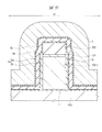
[構造説明]
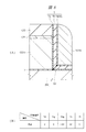
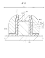
図1および図2は、本実施の形態の半導体装置を示す要部断面図であり、図3は、図1のメモリセル部の断面図である。
[Description of structure]
1 and 2 are main part cross-sectional views showing the semiconductor device of the present embodiment, and FIG. 3 is a cross-sectional view of the memory cell part of FIG.
まず、本実施の形態で説明する半導体装置は、不揮発性メモリ(不揮発性半導体記憶装置、EEPROM、フラッシュメモリ、不揮発性記憶素子)および周辺回路を有する。 First, the semiconductor device described in this embodiment includes a nonvolatile memory (a nonvolatile semiconductor memory device, an EEPROM, a flash memory, and a nonvolatile memory element) and a peripheral circuit.
不揮発性メモリは、電荷蓄積部としてトラップ性絶縁膜(電荷を蓄積可能な絶縁膜)を用いたものである。また、メモリセルMCは、スプリットゲート型のメモリセルである。即ち、制御ゲート電極(選択ゲート電極)CGを有する制御トランジスタ(選択トランジスタ)と、メモリゲート電極(メモリ用ゲート電極)MGを有するメモリトランジスタとの2つのMISFETを接続したものである。 The nonvolatile memory uses a trapping insulating film (an insulating film capable of storing charges) as a charge storage portion. The memory cell MC is a split gate type memory cell. That is, two MISFETs of a control transistor (selection transistor) having a control gate electrode (selection gate electrode) CG and a memory transistor having a memory gate electrode (memory gate electrode) MG are connected.
ここで、電荷蓄積部(電荷蓄積層)を含むゲート絶縁膜およびメモリゲート電極MGを備えるMISFET(Metal Insulator Semiconductor Field Effect Transistor)をメモリトランジスタ(記憶用トランジスタ)といい、また、ゲート絶縁膜および制御ゲート電極CGを備えるMISFETを制御トランジスタ(選択トランジスタ、メモリセル選択用トランジスタ)という。 Here, a MISFET (Metal Insulator Semiconductor Field Effect Transistor) including a gate insulating film including a charge storage portion (charge storage layer) and a memory gate electrode MG is referred to as a memory transistor (memory transistor). The MISFET including the gate electrode CG is referred to as a control transistor (selection transistor, memory cell selection transistor).
周辺回路とは、不揮発性メモリを駆動するための回路であり、例えば、種々の論理回路などにより構成される。種々の論理回路は、例えば、後述するnチャネル型MISFETQnやpチャネル型MISFETなどにより構成される。また、後述する容量素子(ここでは、PIP;Poly-Insulator-Poly)Cなども形成される。 The peripheral circuit is a circuit for driving the nonvolatile memory, and is configured by various logic circuits, for example. The various logic circuits are configured by, for example, an n-channel type MISFET Qn, a p-channel type MISFET, etc., which will be described later. Further, a capacitor element (here, PIP; Poly-Insulator-Poly) C, which will be described later, is also formed.
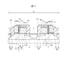
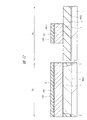
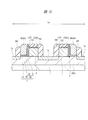
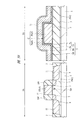
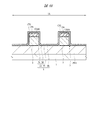
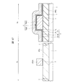
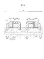
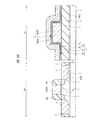
図1および図2に示すように、本実施の形態の半導体装置は、半導体基板1のメモリセル領域1Aに配置された不揮発性メモリのメモリセルMCと、周辺回路領域2Aに配置されたnチャネル型MISFETQnと、周辺回路領域3Aに配置された容量素子Cとを有している。
As shown in FIGS. 1 and 2, the semiconductor device according to the present embodiment includes a memory cell MC of a nonvolatile memory arranged in a
図1に、ドレイン領域(MD)を共有する2つのメモリセルMCの要部断面図を、図2の左部に、nチャネル型MISFETQnの要部断面図を示し、図2の右部に、容量素子Cの要部断面図を示す。 FIG. 1 shows a cross-sectional view of a main part of two memory cells MC sharing a drain region (MD), a cross-sectional view of a main part of an n-channel MISFET Qn on the left part of FIG. 2, and a right part of FIG. The principal part sectional view of capacitive element C is shown.
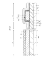
図1に示すように、2つのメモリセルは、ドレイン領域(MD(8b))を挟んでほぼ対称に配置される。なお、メモリセル領域1Aには、さらに、複数のメモリセルMCが配置される。例えば、図1に示すメモリセル領域1Aの左側のメモリセルMCのさらに左にはソース領域(MS)および共有されるドレイン領域(MD)が交互に配置されるようにメモリセルMCが、図1中の左右方向(ゲート長方向)に配置され、メモリセル列を構成している。また、図1の紙面に垂直な方向(ゲート幅方向)にも、メモリセル列が複数配置されている。このように、複数のメモリセルMCがアレイ状に形成されている。
As shown in FIG. 1, the two memory cells are arranged almost symmetrically with the drain region (MD (8b)) interposed therebetween. A plurality of memory cells MC are further arranged in the
図2に示すように、半導体基板(半導体ウエハ)1には、素子を分離するための素子分離領域2が形成されており、この素子分離領域2で区画(分離)された活性領域から、p型ウエルPW1、PW2が露出している。
As shown in FIG. 2, an
なお、メモリセル領域1Aに示される断面部(図1)においては、素子分離領域2は現れないが、メモリセルMCがアレイ状に形成されるメモリセル領域全体は、素子分離領域2で区画されている。さらに、例えば、メモリセル列間(但し、ソース領域(MS)を除く)には、素子分離領域2が配置される等、電気的な分離が必要な箇所には適宜、素子分離領域2が配置される。また、容量素子Cは、素子分離領域2上に形成される。
In the cross-sectional portion (FIG. 1) shown in the
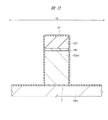
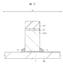
まず、メモリセル領域1AのメモリセルMCの構成について説明する(図1、図3参照)。
First, the configuration of the memory cell MC in the
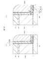
メモリセルMCは、半導体基板1(p型ウエルPW1)の上方に配置された制御ゲート電極(第1ゲート電極)CGと、半導体基板1(p型ウエルPW1)の上方に配置され、制御ゲート電極CGと隣合うメモリゲート電極(第2ゲート電極)MGとを有する。この制御ゲート電極CGの上部には、薄い酸化シリコン膜CP1および窒化シリコン膜(キャップ絶縁膜)CP2が配置されている。メモリセルMCは、さらに、制御ゲート電極CGおよび半導体基板1(p型ウエルPW1)間に配置された絶縁膜3と、メモリゲート電極MGと半導体基板1(p型ウエルPW1)との間に配置され、メモリゲート電極MGと制御ゲート電極CGとの間に配置された絶縁膜5とを有する。また、メモリセルMCは、さらに、半導体基板1のp型ウエルPW1中に形成されたソース領域MSおよびドレイン領域MDを有する。
The memory cell MC is disposed above the semiconductor substrate 1 (p-type well PW1) and the control gate electrode (first gate electrode) CG disposed above the semiconductor substrate 1 (p-type well PW1). The memory gate electrode (second gate electrode) MG adjacent to the CG is included. A thin silicon oxide film CP1 and a silicon nitride film (cap insulating film) CP2 are disposed on the control gate electrode CG. The memory cell MC is further disposed between the control gate electrode CG and the semiconductor substrate 1 (p-type well PW1), and between the memory gate electrode MG and the semiconductor substrate 1 (p-type well PW1). The insulating
制御ゲート電極CGおよびメモリゲート電極MGは、それらの対向側面(側壁)の間に絶縁膜5を介した状態で、半導体基板1の主面上に図1中の左右方向(ゲート長方向)に並んで配置されている。制御ゲート電極CGおよびメモリゲート電極MGの延在方向は、図1の紙面に垂直な方向(ゲート幅方向)である。制御ゲート電極CGおよびメモリゲート電極MGは、ドレイン領域MDおよびソース領域MS間の半導体基板1(p型ウエルPW1)の上部に絶縁膜3、5を介して(但し、制御ゲート電極CGは絶縁膜3を介し、メモリゲート電極MGは絶縁膜5を介して)形成されている。ソース領域MS側にメモリゲート電極MGが位置し、ドレイン領域MD側に制御ゲート電極CGが位置している。なお、本明細書では、ソース領域MSおよびドレイン領域MDを動作時を基準に定義している。後述する書き込み動作時に高電圧を印加する半導体領域をソース領域MSと、書き込み動作時に低電圧を印加する半導体領域をドレイン領域MDと、統一して呼ぶことにする。
The control gate electrode CG and the memory gate electrode MG are arranged in the horizontal direction (gate length direction) in FIG. 1 on the main surface of the
制御ゲート電極CGとメモリゲート電極MGとは、間に絶縁膜5を介在して互いに隣合っており、メモリゲート電極MGは、制御ゲート電極CGの側壁部に絶縁膜5を介してサイドウォールスペーサ状に配置されている。また、絶縁膜5は、メモリゲート電極MGと半導体基板1(p型ウエルPW1)の間の領域と、メモリゲート電極MGと制御ゲート電極CGの間の領域の、両領域にわたって延在している。この絶縁膜5は、後述するように、複数の絶縁膜の積層膜よりなる。
The control gate electrode CG and the memory gate electrode MG are adjacent to each other with the insulating
制御ゲート電極CGと半導体基板1(p型ウエルPW1)の間に形成された絶縁膜3(すなわち制御ゲート電極CGの下の絶縁膜3)が、制御トランジスタのゲート絶縁膜として機能し、メモリゲート電極MGと半導体基板1(p型ウエルPW1)の間の絶縁膜5(すなわちメモリゲート電極MGの下の絶縁膜5)が、メモリトランジスタのゲート絶縁膜(内部に電荷蓄積部を有するゲート絶縁膜)として機能する。
An insulating film 3 (that is, an insulating
絶縁膜3は、例えば酸化シリコン膜または酸窒化シリコン膜などにより形成することができる。また、絶縁膜3として、上述の酸化シリコン膜または酸窒化シリコン膜など以外の、酸化ハフニウム膜、酸化アルミニウム膜(アルミナ)または酸化タンタル膜など、窒化シリコン膜よりも高い誘電率を有する金属酸化膜を使用してもよい。
The insulating
絶縁膜5は、電荷障壁膜と電荷蓄積膜とを有する多層絶縁膜である。ここでは、ONO(oxide-nitride-oxide)膜を用いている。具体的には、第1膜(下層膜)5Aである酸化シリコン膜と、第2膜(中層膜)5Nである窒化シリコン膜と、第3膜(上層膜)5Bである酸化シリコン膜よりなる。第3膜(上層膜)5Bは、それぞれ酸化シリコン膜よりなるサイドウォール膜(側壁膜)5sとデポ膜(堆積膜)5dとの積層膜よりなる。第2膜5Nは、電荷蓄積部である。
The insulating
第1膜(下層膜)5Aは、制御ゲート電極CGの側壁とメモリゲート電極MGの側壁との間に位置する縦部(垂直部)と、半導体基板1(p型ウエルPW1)とメモリゲート電極MGの底部(底面)との間に位置する横部(水平部)とを有する。言い換えれば、第1膜5Aは、制御ゲート電極CGの側壁とメモリゲート電極MGの側壁との間から半導体基板1とメモリゲート電極MGの底部との間にかけて連続的に形成された絶縁膜である。この第1膜(トンネル酸化膜)5Aの横部を介してトンネル現象によりホール(正孔)が第2膜(電荷蓄積部)5Nに注入され、電荷蓄積部に書き込まれた電子の消去動作が行われる。メモリセルの動作については後述する。よって、少なくともこの横部の膜厚が2nm以下であることが好ましい。なお、縦部の膜厚(ゲート長方向の厚さ)は、2nm以上であってもよい。
The first film (lower film) 5A includes a vertical part (vertical part) positioned between the side wall of the control gate electrode CG and the side wall of the memory gate electrode MG, the semiconductor substrate 1 (p-type well PW1), and the memory gate electrode. It has a horizontal part (horizontal part) located between the bottom part (bottom face) of MG. In other words, the
また、第2膜(中層膜)5Nは、第1膜5A上に配置され、制御ゲート電極CGの側壁とメモリゲート電極MGの側壁との間に位置する縦部(垂直部)と、半導体基板1(p型ウエルPW1)とメモリゲート電極MGの底部(底面)との間に位置する横部(水平部)とを有する。言い換えれば、第2膜5Nは、制御ゲート電極CGの側壁とメモリゲート電極MGの側壁との間から半導体基板1とメモリゲート電極MGの底部との間にかけて連続的に形成された絶縁膜である。また、別の言い方をすれば、第2膜5Nは、第1膜5Aの縦部とメモリゲート電極MGの側壁との間に位置する縦部(垂直部)と、第1膜5Aの横部とメモリゲート電極MGの底部(底面)との間に位置する横部(水平部)とを有する。
The second film (intermediate film) 5N is disposed on the
また、第3膜5Bは、前述したように、サイドウォール膜5sとデポ膜5dとの積層膜よりなる。この第3膜5Bは、制御ゲート電極CGの側壁とメモリゲート電極MGの側壁との間に位置する縦部(垂直部)と、半導体基板1(p型ウエルPW1)とメモリゲート電極MGの底部(底面)との間に位置する横部(水平部)とを有する。言い換えれば、第3膜5Bは、制御ゲート電極CGの側壁とメモリゲート電極MGの側壁との間から半導体基板1とメモリゲート電極MGの底部との間にかけて連続的に形成された絶縁膜である。また、別の言い方をすれば、第3膜5Bは、第2膜5Nの縦部とメモリゲート電極MGの側壁との間に位置する縦部(垂直部)と、第2膜5Nの横部とメモリゲート電極MGの底部(底面)との間に位置する横部(水平部)とを有する。この第3膜5Bの縦部は、サイドウォール膜5sとデポ膜5dの縦部との積層部よりなり、横部はデポ膜5dの横部よりなる。
Further, as described above, the
また、サイドウォール膜(側壁膜)5sの高さH5sは、メモリゲート電極MGの高さHMGより低く設定されている(H5s<HMG)。言い換えれば、サイドウォール膜(側壁膜)5sの上部は、メモリゲート電極MGの上部より低い位置に配置されている。 The height H5s of the sidewall film (sidewall film) 5s is set lower than the height HMG of the memory gate electrode MG (H5s <HMG). In other words, the upper portion of the sidewall film (sidewall film) 5s is disposed at a position lower than the upper portion of the memory gate electrode MG.
また、このサイドウォール膜(側壁膜)5sとしては、上記酸化シリコン膜の他、窒化シリコン膜や酸窒化シリコン膜などの絶縁膜を用いることも可能である。ただし、第2膜(電荷蓄積部)5N以外の箇所に、電荷トラップ性の高い窒化膜を配置した場合、この窒化膜内にも電荷が蓄積され、閾値電位(Vth)が変動する恐れがある。よって、サイドウォール膜(側壁膜)5sとしては、酸化シリコン膜や酸窒化シリコン膜を用いることが好ましい。本実施の形態においては、酸化シリコン膜を用いている。 In addition to the silicon oxide film, an insulating film such as a silicon nitride film or a silicon oxynitride film can be used as the sidewall film (sidewall film) 5s. However, if a nitride film having a high charge trapping property is disposed at a place other than the second film (charge storage portion) 5N, charges are also accumulated in the nitride film, and the threshold potential (Vth) may fluctuate. . Therefore, it is preferable to use a silicon oxide film or a silicon oxynitride film as the sidewall film (sidewall film) 5s. In this embodiment, a silicon oxide film is used.
よって、デポ膜5dは、第2膜5Nの横部上からサイドウォール膜5sの側壁を覆うように延在し、さらに、第2膜5Nの縦部の側壁に沿うように延在している。
Therefore, the
第3膜5Bの膜厚について説明する。第3膜の縦部の最大膜厚(T1)は、サイドウォール膜5sの最大膜厚Tsと酸化シリコン膜(デポ膜)5dの縦部の膜厚Tdとの和(Ts+Td)となる。また、第3膜の横部の膜厚(T2)は、酸化シリコン膜(デポ膜)5dの縦部の膜厚Tdとなる。このように、第3膜の縦部の膜厚は、横部の膜厚より大きくなっている(図3参照)。
The film thickness of the
なお、上記においては、絶縁膜5の形状として、図3等に示す側のメモリセルに対応して各積層膜(5A、5N、5B、5d)の形状を説明したが、例えば、図1に示す左側のメモリセルにおいては、各積層膜の形状は、ドレイン領域(MD(8b))を挟んでほぼ線対称な形状となる。
In the above description, the shape of each stacked film (5A, 5N, 5B, 5d) corresponding to the memory cell on the side shown in FIG. 3 and the like has been described as the shape of the insulating
このように、窒化シリコン膜(5N)を酸化シリコン膜(5A)および酸化シリコン膜(5B)で挟んだ構造とすることで、窒化シリコン膜(5N)への電荷の蓄積が可能となる。言い換えれば、絶縁膜5のうち、窒化シリコン膜(5N)は、電荷を蓄積するための絶縁膜であり、電荷蓄積層(電荷蓄積部)として機能する。すなわち、窒化シリコン膜(5N)は、絶縁膜5中に形成されたトラップ性絶縁膜であり、窒化シリコン膜(5N)の上下に位置する酸化シリコン膜(5A、5B)は、電荷ブロック層(電荷ブロック膜、電荷閉じ込め層)として機能する。この酸化シリコン膜(5A)、窒化シリコン膜(5N)および酸化シリコン膜(5B)の積層膜は、ONO膜と呼ばれることもある。なお、ここでは、絶縁膜5をONO膜として説明したが、第2膜5Nを電荷蓄積機能を有する絶縁膜で構成し、第1膜5Aおよび第3膜5B(5s、5d)を、第2膜5Nと異なる絶縁膜を用いて構成すれば、他の絶縁膜の組み合わせでもよい。例えば、電荷蓄積機能を有する絶縁膜(電荷蓄積層)としては、例えば、酸化アルミニウム膜、酸化ハフニウム膜または酸化タンタル膜などの絶縁膜を用いてもよい。これらの膜は、窒化シリコン膜よりも高い誘電率を有する高誘電率膜である。また、シリコンナノドットを有する絶縁膜を電荷蓄積層として用いてもよい。
In this manner, by having a structure in which the silicon nitride film (5N) is sandwiched between the silicon oxide film (5A) and the silicon oxide film (5B), charge can be accumulated in the silicon nitride film (5N). In other words, the silicon nitride film (5N) in the insulating
上記絶縁膜5のうち、メモリゲート電極MGと半導体基板1(p型ウエルPW1)との間の絶縁膜5は、電荷(電子)を保持した状態または電荷を保持しない状態で、メモリトランジスタのゲート絶縁膜として機能する。また、メモリゲート電極MGと制御ゲート電極CGとの間の絶縁膜5は、メモリゲート電極MGと制御ゲート電極CGとの間を絶縁(電気的に分離)するための絶縁膜として機能する。
Among the insulating
メモリゲート電極MG下の絶縁膜5の下にメモリトランジスタのチャネル領域が形成され、制御ゲート電極CG下の絶縁膜3の下に制御トランジスタのチャネル領域が形成される。制御ゲート電極CG下の絶縁膜3の下の制御トランジスタのチャネル形成領域には、制御トランジスタのしきい値調整用の半導体領域(p型半導体領域またはn型半導体領域)が必要に応じて形成されている。メモリゲート電極MG下の絶縁膜5の下のメモリトランジスタのチャネル形成領域には、メモリトランジスタのしきい値調整用の半導体領域(p型半導体領域またはn型半導体領域)が必要に応じて形成されている。
A channel region of the memory transistor is formed under the insulating
前述したとおり、書き込み動作時において、ソース領域MSは、高電圧が印加される半導体領域であり、ドレイン領域MDは低電圧が印加される半導体領域である。これらの領域MS、MDは、n型不純物が導入された半導体領域(n型不純物拡散層)よりなる。 As described above, in the write operation, the source region MS is a semiconductor region to which a high voltage is applied, and the drain region MD is a semiconductor region to which a low voltage is applied. These regions MS and MD are formed of a semiconductor region (n-type impurity diffusion layer) into which an n-type impurity is introduced.
ドレイン領域MDは、LDD(lightly doped drain)構造の領域である。すなわち、ドレイン領域MDは、n−型半導体領域(低濃度不純物拡散層)7bと、n−型半導体領域7bよりも高い不純物濃度を有するn+型半導体領域(高濃度不純物拡散層)8bとを有している。n+型半導体領域8bは、n−型半導体領域7bよりも接合深さが深くかつ不純物濃度が高い。
The drain region MD is a region having an LDD (lightly doped drain) structure. That is, the drain region MD includes an n − type semiconductor region (low concentration impurity diffusion layer) 7b and an n + type semiconductor region (high concentration impurity diffusion layer) 8b having an impurity concentration higher than that of the n −
また、ソース領域MSも、LDD構造の領域である。すなわち、ソース領域MSは、n−型半導体領域(低濃度不純物拡散層)7aと、n−型半導体領域7aよりも高い不純物濃度を有するn+型半導体領域(高濃度不純物拡散層)8aとを有している。n+型半導体領域8aは、n−型半導体領域7aよりも接合深さが深くかつ不純物濃度が高い。
The source region MS is also a region having an LDD structure. That is, the source region MS includes an n − type semiconductor region (low concentration impurity diffusion layer) 7a and an n + type semiconductor region (high concentration impurity diffusion layer) 8a having an impurity concentration higher than that of the n −
メモリゲート電極MGおよび制御ゲート電極CGの合成パターンの側壁部には、酸化シリコンなどの絶縁体(酸化シリコン膜、絶縁膜)からなる側壁絶縁膜(サイドウォール、サイドウォールスペーサ)SWが形成されている。すなわち、絶縁膜5を介して制御ゲート電極CGに隣接する側とは逆側のメモリゲート電極MGの側壁(側面)上と、絶縁膜5を介してメモリゲート電極MGに隣接する側とは逆側の制御ゲート電極CGの側壁(側面)上とに、側壁絶縁膜SWが形成されている。
A sidewall insulating film (sidewall, sidewall spacer) SW made of an insulator (silicon oxide film, insulating film) such as silicon oxide is formed on the sidewall portion of the combined pattern of the memory gate electrode MG and the control gate electrode CG. Yes. That is, the side (side surface) of the memory gate electrode MG opposite to the side adjacent to the control gate electrode CG via the insulating
ソース領域MSのn−型半導体領域7aはメモリゲート電極MGの側壁に対して自己整合的に形成され、n+型半導体領域8aはメモリゲート電極MG側の側壁絶縁膜SWの側面に対して自己整合的に形成されている。このため、低濃度のn−型半導体領域7aはメモリゲート電極MG側の側壁絶縁膜SWの下に形成されている。また、高濃度のn+型半導体領域8aは低濃度のn−型半導体領域7aの外側に形成されている。したがって、低濃度のn−型半導体領域7aはメモリトランジスタのチャネル領域に隣接するように形成され、高濃度のn+型半導体領域8aは低濃度のn−型半導体領域7aに接し、メモリトランジスタのチャネル領域からn−型半導体領域7aの分だけ離間するように形成されている。
The n −
ドレイン領域MDのn−型半導体領域7bは制御ゲート電極CGの側壁に対して自己整合的に形成され、n+型半導体領域8bは制御ゲート電極CG側の側壁絶縁膜SWの側面に対して自己整合的に形成されている。このため、低濃度のn−型半導体領域7bは制御ゲート電極CG側の側壁絶縁膜SWの下に形成されている。また、高濃度のn+型半導体領域8bは低濃度のn−型半導体領域7bの外側に形成されている。したがって、低濃度のn−型半導体領域7bは制御トランジスタのチャネル領域に隣接するように形成され、高濃度のn+型半導体領域8bは低濃度のn−型半導体領域7bに接し、制御トランジスタのチャネル領域からn−型半導体領域7bの分だけ離間するように形成されている。
The n −
制御ゲート電極CGは導電性膜(導電体膜)からなるが、好ましくは多結晶シリコン膜のようなシリコン膜4からなる。シリコン膜4は、例えば、n型のシリコン膜(n型不純物を導入した多結晶シリコン膜、ドープトポリシリコン膜)であり、n型不純物が導入されて低抵抗率とされている。
The control gate electrode CG is made of a conductive film (conductor film), but is preferably made of a
メモリゲート電極MGは導電性膜(導電体膜)からなり、図1および図2に示すように、例えば、多結晶シリコン膜のようなシリコン膜6により形成されている。
The memory gate electrode MG is made of a conductive film (conductor film), and is formed of a
メモリゲート電極MGの上部(上面)とn+型半導体領域8aおよびn+型半導体領域8bの上面(表面)には、金属シリサイド層(金属シリサイド膜)11が形成されている。金属シリサイド層11は、例えばコバルトシリサイド層またはニッケルシリサイド層などからなる。金属シリサイド層11により、拡散抵抗やコンタクト抵抗を低抵抗化することができる。また、メモリゲート電極MGと制御ゲート電極CGとの間のショートをできるだけ防止するという観点から、メモリゲート電極MGと制御ゲート電極CGの一方または両方の上部に金属シリサイド層11を形成しない場合もあり得る。
A metal silicide layer (metal silicide film) 11 is formed on the top (upper surface) of the memory gate electrode MG and on the upper surfaces (front surfaces) of the n +
次いで、周辺回路領域2Aのnチャネル型MISFETQnについて説明する。
Next, the n-channel MISFET Qn in the
図2の左側に示すように、nチャネル型MISFETQnは、周辺回路領域2Aに配置される。このnチャネル型MISFETQnは、半導体基板1(p型ウエルPW2)の上方に配置されたゲート電極GEと、ゲート電極GEと半導体基板1(p型ウエルPW2)間に配置された絶縁膜3と、ゲート電極GEの両側の半導体基板1(p型ウエルPW2)中に形成されたソース、ドレイン領域(7、8)を有する。
As shown on the left side of FIG. 2, the n-channel MISFET Qn is arranged in the
ゲート電極GEの延在方向は、図1の紙面に垂直な方向(ゲート幅方向)である。ゲート電極GEと半導体基板1(p型ウエルPW2)間に配置された絶縁膜3が、nチャネル型MISFETQnのゲート絶縁膜として機能する。ゲート電極GE下の絶縁膜3の下にnチャネル型MISFETQnのチャネル領域が形成される。
The extending direction of the gate electrode GE is a direction (gate width direction) perpendicular to the paper surface of FIG. The insulating
ソース、ドレイン領域(7、8)は、LDD構造を有し、n+型半導体領域8とn−型半導体領域7よりなる。n+型半導体領域8は、n−型半導体領域7よりも接合深さが深くかつ不純物濃度が高い。
The source and drain regions (7, 8) have an LDD structure and are composed of an n +
ゲート電極GEの側壁部には、酸化シリコンなどの絶縁体(酸化シリコン膜、絶縁膜)からなる側壁絶縁膜(サイドウォール、サイドウォールスペーサ)SWが形成されている。 A sidewall insulating film (sidewall, sidewall spacer) SW made of an insulator (silicon oxide film, insulating film) such as silicon oxide is formed on the sidewall portion of the gate electrode GE.
n−型半導体領域7はゲート電極GEの側壁に対して自己整合的に形成されている。このため、低濃度のn−型半導体領域7はゲート電極GEの側壁部の側壁絶縁膜SWの下に形成される。したがって、低濃度のn−型半導体領域7はMISFETのチャネル領域に隣接するように形成されている。また、n+型半導体領域8は側壁絶縁膜SWの側面に対して自己整合的に形成されている。このように、低濃度のn−型半導体領域7はMISFETのチャネル領域に隣接するように形成され、高濃度のn+型半導体領域8は低濃度のn−型半導体領域7に接し、MISFETのチャネル領域からn−型半導体領域7の分だけ離間するように形成されている。
The n −
ゲート電極GEは導電性膜(導電体膜)からなるが、例えば、上記制御ゲート電極CGと同様に、n型多結晶シリコン膜(n型不純物を導入した多結晶シリコン膜、ドープトポリシリコン膜)のようなシリコン膜4で構成することが好ましい。
The gate electrode GE is composed of a conductive film (conductor film). For example, similarly to the control gate electrode CG, an n-type polycrystalline silicon film (polycrystalline silicon film doped with n-type impurities, doped polysilicon film) It is preferable to use the
ゲート電極GEの上部(上面)とn+型半導体領域8の上面(表面)には、金属シリサイド層11が形成されている。金属シリサイド層11は、例えばコバルトシリサイド層またはニッケルシリサイド層などからなる。金属シリサイド層11により、拡散抵抗やコンタクト抵抗を低抵抗化することができる。
A
次いで、周辺回路領域3Aの容量素子Cについて説明する。図2の右側に示すように、容量素子Cは、周辺回路領域3Aに配置される。この容量素子Cは、ここでは、PIP構成を有している。具体的には、上部電極Paと下部電極Pbとを有し、これらの電極の間に、容量絶縁膜として上記絶縁膜5(5A、5N、5B(5s、5d))が配置されている。下部電極Pbは、上記ゲート電極GEおよび上記制御ゲート電極CGと同様に、n型多結晶シリコン膜(n型不純物を導入した多結晶シリコン膜、ドープトポリシリコン膜)のようなシリコン膜4で構成する。また、上部電極Paは、上記メモリゲート電極MGと同様に、多結晶シリコン膜のようなシリコン膜6で構成する。なお、下部電極Pbの下層には、絶縁膜(3)が配置されている。また、上部電極Paの表面には、金属シリサイド層11が配置されている。
Next, the capacitive element C in the
下部電極Pbの上面には、絶縁膜5(5A、5N、5B(5d))が配置され、下部電極Pbの側面には、絶縁膜5(5A、5N、5B(5s、5d))が配置されている。ここで、下部電極Pbの側面には、絶縁膜5を覆うように上部電極Paが配置され、上部電極Paに下部電極Pbの側面から半導体基板1上に延在する部分に角部を有することになり、この部分で電界が集中し易くなるため容量素子Cの信頼性が低下する畏れがある。しかし、本実施の形態の容量素子Cのように、下部電極Pbの側面に絶縁膜5が配置されることで、下部電極の角部における電界を緩和することができ、容量素子Cの信頼性を向上させることが可能となる。さらに、下部電極Pbの側面に絶縁膜5が配置されることで、容量素子Cの側面における容量値が小さくなり、下部電極Pbと上部電極Paが平面的に重なる領域のみが容量として寄与するため、容量素子Cの容量の設計値における誤差が小さくなり、半導体装置の歩留まりを向上させることが可能となる。
The insulating film 5 (5A, 5N, 5B (5d)) is disposed on the upper surface of the lower electrode Pb, and the insulating film 5 (5A, 5N, 5B (5s, 5d)) is disposed on the side surface of the lower electrode Pb. Has been. Here, the upper electrode Pa is disposed on the side surface of the lower electrode Pb so as to cover the insulating
[動作説明]
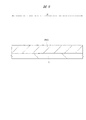
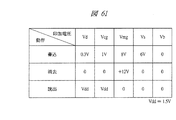
図4は、メモリセルMCの等価回路図である。図示するように、ドレイン領域(MD)とソース領域(MS)との間に、メモリトランジスタと制御トランジスタとが直列に接続され一つのメモリセルを構成する。図5は、本実施の形態の「書込」、「消去」および「読出」時における選択メモリセルの各部位への電圧の印加条件の一例を示す表である。図5の表には、「書込」、「消去」および「読出」時のそれぞれにおいて、メモリゲート電極MGに印加する電圧Vmg、ソース領域(ソース領域MS)に印加する電圧Vs、制御ゲート電極CGに印加する電圧Vcg、ドレイン領域(ドレイン領域MD)に印加する電圧Vd(例えば、Vdd=1.5V)、およびp型ウエルPW1に印加される電圧Vbが記載されている。なお、図5の表に示したものは電圧の印加条件の好適な一例であり、これに限定されるものではなく、必要に応じて種々変更可能である。また、本実施の形態では、メモリトランジスタの絶縁膜5中の電荷蓄積層(電荷蓄積部)である窒化シリコン膜(5N)への電子の注入を「書込」、ホール(hole:正孔)の注入を「消去」と定義する。
[Description of operation]
FIG. 4 is an equivalent circuit diagram of the memory cell MC. As shown in the figure, a memory transistor and a control transistor are connected in series between a drain region (MD) and a source region (MS) to constitute one memory cell. FIG. 5 is a table showing an example of voltage application conditions to each part of the selected memory cell at the time of “write”, “erase”, and “read” in the present embodiment. The table of FIG. 5 shows the voltage Vmg applied to the memory gate electrode MG, the voltage Vs applied to the source region (source region MS), and the control gate electrode at the time of “write”, “erase”, and “read”. A voltage Vcg applied to CG, a voltage Vd applied to the drain region (drain region MD) (for example, Vdd = 1.5 V), and a voltage Vb applied to the p-type well PW1 are described. In addition, what was shown in the table | surface of FIG. 5 is a suitable example of the application conditions of a voltage, It is not limited to this, A various change is possible as needed. In the present embodiment, the electron injection into the silicon nitride film (5N), which is the charge storage layer (charge storage portion) in the insulating
書込み方式は、いわゆるSSI(Source Side Injection:ソースサイド注入)方式と呼ばれるホットエレクトロン書込みを用いることができる。例えば図5の「書込」の欄に示されるような電圧を、書込みを行う選択メモリセルの各部位に印加し、選択メモリセルの絶縁膜5中の窒化シリコン膜(5N)中に電子(エレクトロン)を注入する。ホットエレクトロンは、2つのゲート電極(メモリゲート電極MGおよび制御ゲート電極CG)間の下のチャネル領域(ソース、ドレイン間)で発生し、メモリゲート電極MGの下の絶縁膜5中の電荷蓄積層(電荷蓄積部)である窒化シリコン膜(5N)にホットエレクトロンが注入される。注入されたホットエレクトロン(電子)は、絶縁膜5中の窒化シリコン膜(5N)中のトラップ準位に捕獲され、その結果、メモリトランジスタのしきい値電圧が上昇する。
As the writing method, hot electron writing called a so-called SSI (Source Side Injection) method can be used. For example, a voltage as shown in the “write” column of FIG. 5 is applied to each part of the selected memory cell to be written, and electrons (5N) in the insulating
消去方法は、直接トンネル現象を利用したホール注入による消去方式を用いることができる。すなわち、直接トンネル現象によりホールを電荷蓄積部(絶縁膜5中の窒化シリコン膜(5N))に注入することにより消去を行う。例えば図5の「消去」の欄に示すように、メモリゲート電極MG(Vmg)に、例えば、−11Vの負電位を印加し、p型ウエルPW1(Vb)を、例えば、0Vとする。これにより、窒化シリコン膜(5N)を介して直接トンネル現象により生じたホールが電荷蓄積部(絶縁膜5中の窒化シリコン膜(5N))に注入され、窒化シリコン膜(5N)中のエレクトロン(電子)を相殺する、もしくは注入されたホールが窒化シリコン膜(5N)中のトラップ準位に捕獲されることにより消去動作を行う。これによりメモリトランジスタのしきい値電圧が低下する(消去状態となる)。直接トンネル現象を利用するためには、窒化シリコン膜(5N)の下層の酸化シリコン膜(5A)の膜厚を2nm以下とし、VmgとVbとの電位差を−8〜−14Vとすることが好ましい。このような消去方法を用いた場合には、いわゆるBTBT(Band-To-Band Tunneling:バンド間トンネル現象)消去を用いた場合(図6(B)参照)と比較し、消費電流を低減することができる。 As an erasing method, an erasing method by hole injection using a direct tunnel phenomenon can be used. That is, erasing is performed by injecting holes into the charge storage portion (silicon nitride film (5N) in the insulating film 5) by direct tunneling. For example, as shown in the “erase” column of FIG. 5, a negative potential of, for example, −11 V is applied to the memory gate electrode MG (Vmg), and the p-type well PW1 (Vb) is set to, for example, 0 V. As a result, holes generated by the tunnel phenomenon directly through the silicon nitride film (5N) are injected into the charge storage portion (the silicon nitride film (5N) in the insulating film 5), and electrons in the silicon nitride film (5N) ( The electrons are offset or the injected holes are captured by trap levels in the silicon nitride film (5N), thereby performing an erase operation. This lowers the threshold voltage of the memory transistor (becomes an erased state). In order to use the direct tunnel phenomenon, it is preferable that the thickness of the silicon oxide film (5A) under the silicon nitride film (5N) is 2 nm or less and the potential difference between Vmg and Vb is −8 to −14V. . When such an erasing method is used, current consumption is reduced as compared with a case where so-called BTBT (Band-To-Band Tunneling) erasing is used (see FIG. 6B). Can do.
読出し時には、例えば図5の「読出」の欄に示されるような電圧を、読出しを行う選択メモリセルの各部位に印加する。読出し時のメモリゲート電極MGに印加する電圧Vmgを、書込み状態におけるメモリトランジスタのしきい値電圧と消去状態におけるメモリトランジスタのしきい値電圧との間の値にすることで、メモリセルに電流が流れるか否かで、書込み状態と消去状態とを判別することができる。 At the time of reading, for example, a voltage as shown in the “read” column in FIG. 5 is applied to each part of the selected memory cell to be read. By setting the voltage Vmg applied to the memory gate electrode MG at the time of reading to a value between the threshold voltage of the memory transistor in the writing state and the threshold voltage of the memory transistor in the erasing state, current flows in the memory cell. The writing state and the erasing state can be discriminated depending on whether or not it flows.
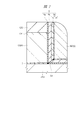
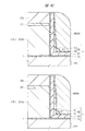
<1>このように、本実施の形態によれば、絶縁膜(ONO膜)5を構成する第3膜(酸化シリコン膜)5Bを、サイドウォール膜(側壁膜)5sとデポ膜(堆積膜)5dとの積層膜で構成したので、メモリゲート電極MGの角部と半導体基板(PW1)間において、絶縁膜5の角部における上面と下面との距離D1を大きくすることができる(図3参照)。その結果、当該部位における電界集中を緩和でき、消去特性を向上させることができる。
<1> Thus, according to the present embodiment, the third film (silicon oxide film) 5B constituting the insulating film (ONO film) 5 is divided into the sidewall film (sidewall film) 5s and the deposition film (deposited film). ) 5d, the distance D1 between the upper surface and the lower surface at the corner of the insulating
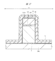
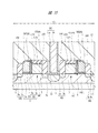
図6は、本実施の形態の比較例のメモリセルおよびその印加電圧を示す図である。図6(A)は、比較例のメモリセル部の構成を示す要部断面図で、図6(B)は、BTBT消去を用いた場合の印加電圧の一例である。図6(A)に示すように、サイドウォール膜5sを省略した比較例のメモリセルにおいては、メモリゲート電極MGの角部と半導体基板(PW1)間において、絶縁膜5の角部における上面と下面との距離D2が小さく(D2<D1)、当該部位において、電界集中が生じ、消去特性が劣化する。
FIG. 6 is a diagram showing a memory cell of a comparative example of the present embodiment and its applied voltage. FIG. 6A is a cross-sectional view of a main part showing a configuration of a memory cell portion of a comparative example, and FIG. 6B is an example of an applied voltage when BTBT erase is used. As shown in FIG. 6A, in the memory cell of the comparative example in which the
即ち、メモリゲート電極MGの角部において、電界集中が生じ、メモリゲート電極MGから酸化シリコン膜を介してFN(Fowler Nordheim)トンネル現象により、窒化シリコン膜(5N)中に電子(エレクトロン)が注入される。その結果、消去動作(ホール注入)が抑制され、消去特性が悪くなる。また、電子(エレクトロン)の注入量が多くなれば、消去ができず、メモリトランジスタのしきい値電圧を上昇させ、書込み状態が保持される恐れもある。 That is, electric field concentration occurs at the corner of the memory gate electrode MG, and electrons (electrons) are injected from the memory gate electrode MG through the silicon oxide film into the silicon nitride film (5N) by the FN (Fowler Nordheim) tunnel phenomenon. Is done. As a result, the erase operation (hole injection) is suppressed, and the erase characteristics are deteriorated. Further, if the injection amount of electrons (electrons) increases, erasing cannot be performed, the threshold voltage of the memory transistor is increased, and the written state may be maintained.
これに対し、本実施の形態によれば、サイドウォール膜5sを形成したので、メモリゲート電極MGの側面の底部と半導体基板(PW1)との距離D1を比較例の距離D2より大きくでき、当該部位におけるFNトンネル現象の発生を抑制することができる。これにより、消去(ホール注入)を効率的に行うことができ、消去特性を向上させることができる。特に、図3に示すように、本実施の形態の構造においては、サイドウォール膜5sをメモリゲート電極MGと窒化シリコン膜(5N)との間に形成しているため、消去動作時におけるメモリゲート電極MG側からの電子の注入をより効果的に抑制することが可能となる。
On the other hand, according to the present embodiment, since the
図8は、本実施の形態のメモリセルと比較例のメモリセルの消去特性を示すグラフである。横軸は、消去電位の印加時間[Time(s)]を、縦軸は、閾値電位[Vth(a.u.)]を示す。なお、1.E−0n(n;整数)は、1×10−n[s]を示す。 FIG. 8 is a graph showing erase characteristics of the memory cell of this embodiment and the memory cell of the comparative example. The horizontal axis represents the erase potential application time [Time (s)], and the vertical axis represents the threshold potential [Vth (au)]. In addition, 1. E-0n (n; integer) represents 1 × 10 −n [s].
グラフ(a)は、比較例のメモリセルの場合を示す。この場合、しきい値電圧の低下が緩やかなグラフとなっている。これに対し、グラフ(b)に示す本実施の形態の場合は、消去電位の印加時間に応じて急速にしきい値電圧が低下しており、消去動作(ホール注入)が効率的に行われていることが分かる。 Graph (a) shows the case of the memory cell of the comparative example. In this case, the threshold voltage decreases slowly. On the other hand, in the case of the present embodiment shown in the graph (b), the threshold voltage decreases rapidly according to the application time of the erase potential, and the erase operation (hole injection) is performed efficiently. I understand that.
また、直接トンネル現象を利用したホール注入による消去方式を用いることで、上記BTBT消去を用いた場合と比較し、消費電流10万分の1(1/105)〜100万分の1(1/106)まで低下させることができた。前述したように、図6(B)に、BTBT消去を用いた場合の印加電圧の一例を示す。 In addition, by using an erasing method by hole injection using a direct tunnel phenomenon, current consumption is reduced from 1 / 100,000 (1/10 5 ) to 1 / 1,000,000 (1/10) as compared with the case of using BTBT erasing. 6 ). As described above, FIG. 6B shows an example of an applied voltage when BTBT erase is used.
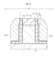
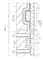
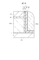
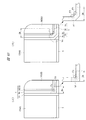
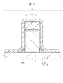
<2>また、サイドウォール膜(側壁膜)5sの高さH5sを、メモリゲート電極MGの高さHMGより低く設定した(H5s<HMG)。即ち、半導体基板1の上面とメモリゲート電極MGの下面との間に形成された絶縁膜5の膜厚が、金属シリサイド層11と窒化シリコン膜CP2との間に形成された絶縁膜5の膜厚と実質的に等しくなるようにした。このとき、サイドウォール膜(側壁膜)5sの上方にもメモリゲート電極MGが延在し、サイドウォール膜5sの側壁がメモリゲート電極MGを形成するシリコン膜6で覆われることとなる。図7は、本実施の形態の半導体装置の他のメモリセル部の構成を示す要部断面図である。図7に示すメモリセルにおいては、図3に示すメモリセルと等しいメモリゲート電極MGのゲート長を有するメモリセルであって、サイドウォール膜(側壁膜)5sの高さH5sをメモリゲート電極MGの高さHMGと同じにしてある(H5s=HMG)。このような形状のメモリセルに対し、図3に示すメモリセルにおいては、サイドウォール膜(側壁膜)5sの上方にもメモリゲート電極MGが延在している分、メモリゲート電極MGの断面積を増加させることが可能となる。これにより、メモリゲート電極MGの抵抗を低減することができ、メモリセルの動作を高速化させ、メモリ動作特性を向上させることができる。さらに、サイドウォール膜(側壁膜)5sの上方にもメモリゲート電極MGが延在していることにより、その表面の金属シリサイド層11の形成領域を、サイドウォール膜5sの膜厚(ゲート長方向の膜厚)に対応する分だけ、大きく確保することができる。即ち、メモリゲート電極のサイドウォール膜5sと平面的に重なる領域にも金属シリサイド層11を形成することが可能となる。これにより、メモリゲート電極MGの抵抗をさらに低減することができ、メモリセルの動作を高速化させ、メモリ動作特性を向上させることができる。なお、サイドウォール膜(側壁膜)5sの高さH5sは、後述のエッチバック工程のエッチング制御性を考慮すれば、制御ゲート電極CGの高さHCGより高く設定することが好ましい(H5s>HCG、図3参照)。また、メモリゲート電極MGと制御ゲート電極CGとの耐圧を確保するという点からも、制御ゲート電極CGの高さHCGより高く設定することが好ましい。
<2> The height H5s of the sidewall film (sidewall film) 5s is set lower than the height HMG of the memory gate electrode MG (H5s <HMG). That is, the insulating
上記のように、制御ゲート電極CG上に絶縁膜となる酸化シリコン膜CP1と窒化シリコン膜CP2を形成している場合には、制御ゲート電極CG上にシリサイド膜が形成されない。よって、酸化シリコン膜CP1と窒化シリコン膜CP2を形成せず、制御ゲート電極CG上にシリサイド膜11を形成する場合(図39参照)と異なり、メモリゲート電極MG上のシリサイド膜と制御ゲート電極CG上のシリサイド膜とのショート(短絡)を考慮する必要がない。そのため、上記のとおり、サイドウォール膜(側壁膜)5sの上方にもメモリゲート電極MGを延在させることができ、メモリゲート電極MGの抵抗を低減することができる。このように、制御ゲート電極CGの高さHCGより高くする構成は、酸化シリコン膜CP1と窒化シリコン膜CP2を用いる構成に適用して有用である。
As described above, when the silicon oxide film CP1 and the silicon nitride film CP2 which are insulating films are formed on the control gate electrode CG, the silicide film is not formed on the control gate electrode CG. Therefore, unlike the case where the
<3>また、サイドウォール膜(側壁膜)5sの高さH5sを低くするようにエッチバックする際、エッチバック量(サイドウォール膜5sの後退量)を大きくすることで、サイドウォール膜5sの側面をテーパー形状とすることができる。言い換えれば、サイドウォール膜5sの側面と、窒化シリコン膜(5N)とのなす角を90°より大きくすることができる。これに対応して、デポ膜5dおよびメモリゲート電極MGが形成されるため、メモリゲート電極MGの角部の角度も90°より大きくなる(図3、図39および図40等参照)。なお、かかるテーパー形状については、後述の変形例1においてさらに詳細に説明する。
<3> Further, when etching back so that the height H5s of the sidewall film (sidewall film) 5s is lowered, the etchback amount (retraction amount of the
このように、メモリゲート電極MGの角部を90°より大きくする(ラウンド化させる)ことで、メモリゲート電極MGの角部における電界集中を緩和し、FNトンネル現象の発生を抑制することができる。これにより、消去(ホール注入)を効率的に行うことができ、消去特性を向上させることができる。なお、上記エッチバック工程については、後述の「製法説明」の欄において詳細に説明する。 Thus, by making the corner of the memory gate electrode MG larger than 90 ° (rounding), the electric field concentration at the corner of the memory gate electrode MG can be alleviated and the occurrence of the FN tunnel phenomenon can be suppressed. . As a result, erasing (hole injection) can be performed efficiently, and erasing characteristics can be improved. The etch back process will be described in detail in the “Production Method Description” section below.
[製法説明]
次いで、図9〜図38を参照しながら、本実施の形態の半導体装置の製造方法を説明するとともに、当該半導体装置の構成をより明確にする。図9〜図38は、本実施の形態の半導体装置の製造工程を示す要部断面図である。このうち、図15〜図22は、メモリセル領域の要部断面図である。なお、前述したように、1Aは、メモリセル領域を、2Aおよび3Aは、周辺回路領域を示し、2Aには、nチャネル型MISFETQnが、3Aには、容量素子Cが形成される。
[Product description]
Next, with reference to FIGS. 9 to 38, the method for manufacturing the semiconductor device of the present embodiment will be described, and the configuration of the semiconductor device will be clarified. 9 to 38 are main-portion cross-sectional views illustrating the manufacturing steps of the semiconductor device of the present embodiment. Among these, FIGS. 15 to 22 are cross-sectional views of main parts of the memory cell region. As described above, 1A represents a memory cell region, 2A and 3A represent peripheral circuit regions, n-channel MISFET Qn is formed in 2A, and capacitive element C is formed in 3A.
まず、図9および図10に示すように、半導体基板(半導体ウエハ)1として、例えば1〜10Ωcm程度の比抵抗を有するp型の単結晶シリコンからなるシリコン基板を準備する。なお、シリコン基板以外の半導体基板1を用いてもよい。
First, as shown in FIGS. 9 and 10, a silicon substrate made of p-type single crystal silicon having a specific resistance of, for example, about 1 to 10 Ωcm is prepared as the semiconductor substrate (semiconductor wafer) 1. A
次いで、半導体基板1の主面に素子分離領域2を形成する。例えば、半導体基板1中に素子分離溝を形成し、この素子分離溝の内部に絶縁膜を埋め込むことにより、素子分離領域2を形成する(図10)。このような素子分離法は、STI(Shallow Trench Isolation)法と呼ばれる。この他、LOCOS(Local Oxidization of Silicon)法などを用いて素子分離領域2を形成してもよい。なお、メモリセル領域1Aに示される断面部(図9)においては、素子分離領域2は現れないが、前述したように素子分離領域2が配置される等、電気的な分離が必要な箇所には適宜、素子分離領域2が配置される。
Next, the
次いで、半導体基板1のメモリセル領域1Aにp型ウエルPW1を、半導体基板1の周辺回路領域2Aにp型ウエルPW2を、それぞれ形成する。p型ウエルPW1、PW2は、p型不純物(例えばホウ素(B)など)をイオン注入することによって形成する。なお、ここでは、図10に示すように、周辺回路領域3Aに形成された素子分離領域2の下部にもp型ウエルPW2が薄く配置されている。
Next, a p-type well PW1 is formed in the
次いで、希釈フッ酸洗浄などによって半導体基板1(p型ウエルPW1、PW2)の表面を清浄化した後、図11および図12に示すように、半導体基板1の主面(p型ウエルPW1、PW2の表面)に、絶縁膜(ゲート絶縁膜)3として、例えば、酸化シリコン膜を熱酸化法により、2〜3nm程度の膜厚で形成する。絶縁膜3としては、酸化シリコン膜の他、酸窒化シリコン膜などの他の絶縁膜を用いてもよい。また、この他、酸化ハフニウム膜、酸化アルミニウム膜(アルミナ)または酸化タンタル膜など、窒化シリコン膜よりも高い誘電率を有する金属酸化膜、および酸化膜等と金属酸化膜との積層膜を形成してもよい。また、熱酸化法の他、CVD(Chemical Vapor Deposition:化学的気相成長)法を用いて形成してもよい。また、メモリセル領域1A上の絶縁膜(ゲート絶縁膜)3と周辺回路領域2A上の絶縁膜(ゲート絶縁膜)3を異なる膜厚とし、また、異なる膜種で構成してもよい。
Next, after cleaning the surface of the semiconductor substrate 1 (p-type wells PW1, PW2) by dilute hydrofluoric acid cleaning or the like, as shown in FIGS. 11 and 12, the main surface of the semiconductor substrate 1 (p-type wells PW1, PW2). As an insulating film (gate insulating film) 3, for example, a silicon oxide film is formed with a film thickness of about 2 to 3 nm by a thermal oxidation method. As the insulating
次に、半導体基板1の全面上に、導電性膜(導電体膜)としてシリコン膜4を形成する。このシリコン膜4として、例えば、多結晶シリコン膜をCVD法などを用いて、100〜200nm程度の膜厚で形成する。シリコン膜4として、非晶質シリコン膜を堆積し、熱処理を施すことにより結晶化させてもよい。このシリコン膜4は、メモリセル領域1Aにおいて制御ゲート電極CGとなり、周辺回路領域2Aにおいてnチャネル型MISFETQnのゲート電極GEとなり、周辺回路領域3Aにおいて容量素子Cの下部電極Pbとなる。
Next, a
次いで、メモリセル領域1Aのシリコン膜4中に、n型不純物(例えばヒ素(As)またはリン(P)など)を注入する。
Next, an n-type impurity (such as arsenic (As) or phosphorus (P)) is implanted into the
次いで、シリコン膜4の表面を例えば6nm程度、熱酸化することにより、薄い酸化シリコン膜CP1を形成する。なお、この酸化シリコン膜CP1をCVD法を用いて形成してもよい。次いで、酸化シリコン膜CP1の上部に、CVD法などを用いて、80〜90nm程度の窒化シリコン膜(キャップ絶縁膜)CP2を形成する。
Next, a thin silicon oxide film CP1 is formed by thermally oxidizing the surface of the
次いで、制御ゲート電極CGの形成予定領域に、フォトリソグラフィ法を用いてフォトレジスト膜(図示せず)を形成し、このフォトレジスト膜をマスクとして用いて、窒化シリコン膜CP2、酸化シリコン膜CP1およびシリコン膜4をエッチングする。この後、フォトレジスト膜をアッシングなどにより除去することにより、制御ゲート電極CG(例えば、ゲート長が80nm程度)を形成する。このような、フォトリソグラフィからフォトレジスト膜の除去までの一連の工程をパターニングという。なお、ここでは、制御ゲート電極CGの上部に、窒化シリコン膜CP2および酸化シリコン膜CP1を形成したが、これらの膜を省略することも可能である(図39参照)。この場合、制御ゲート電極CGの高さは適宜調整可能であり、制御ゲート電極CGの高さを窒化シリコン膜CP2を設けた場合の窒化シリコン膜CP2の高さと同程度としてもよい。
Next, a photoresist film (not shown) is formed using a photolithography method in a region where the control gate electrode CG is to be formed, and using this photoresist film as a mask, a silicon nitride film CP2, a silicon oxide film CP1, and The
ここで、メモリセル領域1Aにおいて、制御ゲート電極CGの下に残存する絶縁膜3が、制御トランジスタのゲート絶縁膜となる。なお、制御ゲート電極CGで覆われた部分以外の絶縁膜3は、以降のパターニング工程などにより除去され得る。
Here, in the
次いで、周辺回路領域2A及び周辺回路領域3Aの窒化シリコン膜CP2および酸化シリコン膜CP1をエッチングにより除去する(図14参照)。
Next, the silicon nitride film CP2 and the silicon oxide film CP1 in the
次いで、図13および図14に示すように、制御ゲート電極CG(4)の表面(上面および側面)上を含む半導体基板1上に、絶縁膜5(5A、5N、5B)を形成する。この絶縁膜5の形成工程については、メモリセル領域1Aの要部断面図である図15〜図22を参照しながら詳細に説明する。なお、図15〜図22においては、図面を解かりやすくするため、制御ゲート電極CGの幅(ゲート長)を他の部位に比べ短く表示してある。
Next, as shown in FIGS. 13 and 14, an insulating film 5 (5A, 5N, 5B) is formed on the
まず、半導体基板1の主面を清浄化処理した後、図15に示すように、制御ゲート電極CGの上面および側面上を含む半導体基板1(p型ウエルPW1)上に酸化シリコン膜5Aを形成する。この酸化シリコン膜5Aは、例えば、熱酸化法(好ましくはISSG(In Situ Steam Generation)酸化)により例えば1.6nm程度の膜厚で形成する。なお、酸化シリコン膜5AをCVD法を用いて形成してもよい。図においては、CVD法で形成した場合の酸化シリコン膜5Aの形状を示してある。前述したように、直接トンネル消去方法を用いるためには、絶縁膜(ONO膜)5を構成する第1膜(下層膜)である酸化シリコン膜5Aの膜厚は、2nm以下が好ましい。次いで、図16に示すように、酸化シリコン膜5A上に、窒化シリコン膜5NをCVD法で例えば16nm程度の膜厚で堆積する。この窒化シリコン膜5Nは、酸化シリコン膜5Aを介して、制御ゲート電極CGの上面および側面の上部および半導体基板1(p型ウエルPW1)の上部に位置する。前述したように、この窒化シリコン膜5Nが、メモリセルの電荷蓄積部となり、絶縁膜(ONO膜)5を構成する第2膜(中層膜)となる。
First, after cleaning the main surface of the
次いで、図17に示すように、窒化シリコン膜5N上に、酸化シリコン膜(5s)をCVD法により例えば5nm〜10nm程度の膜厚で堆積する。この酸化シリコン膜(5s)は、酸化シリコン膜5Aおよび窒化シリコン膜5Nを介して、制御ゲート電極CGの上面および側面の上部および半導体基板1(p型ウエルPW1)の上部に位置する。次いで、酸化シリコン膜(5s)をその表面から異方的にエッチング(エッチバック)する。この工程により、図18に示すように、制御ゲート電極CGの両側の側壁部に、酸化シリコン膜5Aおよび窒化シリコン膜5Nを介して、酸化シリコン膜(5s)よりなるサイドウォール膜5sを残存させることができる。酸化シリコン膜(5s)のゲート長方向の膜厚(最大膜厚)は、例えば、5nm〜10nm程度である。
Next, as shown in FIG. 17, a silicon oxide film (5 s) is deposited on the
上記異方的なエッチングとしては、例えば、CF4およびCHF3の混合ガスをエッチングガスとして、プラズマ下でドライエッチングすることができる。 As the anisotropic etching, for example, dry etching can be performed under plasma using a mixed gas of CF 4 and CHF 3 as an etching gas.
この際、エッチバック量を多くし、サイドウォール膜(側壁膜)5sの上部が、窒化シリコン膜(キャップ絶縁膜)CP2の上部(上面)より低くなるまでエッチバックする。このように、サイドウォール膜(側壁膜)5sの高さH5sを調整することで、サイドウォール膜(側壁膜)5sの高さH5sが、メモリゲート電極MGの高さHMGより低くなる(H5s<HMG、図3等参照)。なお、この際、周辺回路領域3Aにおいて、容量素子Cを構成する下部電極Pbの側壁部にもサイドウォール膜(側壁膜)5sが形成される。ここでも、サイドウォール膜(側壁膜)5sの高さH5sは、下部電極Pbの高さHPbより低くなる(H5s<HPb、図2参照)。
At this time, the etching back amount is increased, and etching back is performed until the upper portion of the sidewall film (sidewall film) 5s becomes lower than the upper portion (upper surface) of the silicon nitride film (cap insulating film) CP2. In this way, by adjusting the height H5s of the sidewall film (sidewall film) 5s, the height H5s of the sidewall film (sidewall film) 5s becomes lower than the height HMG of the memory gate electrode MG (H5s < HMG, see FIG. 3 etc.). At this time, in the
また、エッチバック量が大きくなりすぎると、サイドウォール膜5sの膜厚が小さくなりすぎる恐れがあるため、このエッチバック工程のエッチング制御性を考慮し、制御ゲート電極CGの高さHCGよりは高くなる程度に、サイドウォール膜(側壁膜)5sの高さH5sを設定することが好ましい(H5s>HCG)。
If the etch back amount becomes too large, the thickness of the
また、窒化シリコン膜CP2および酸化シリコン膜CP1を形成しない場合においては、これらの膜の代わりに制御ゲート電極CGが配置される構成となる。即ち、窒化シリコン膜CP2の上面の高さが、制御ゲート電極CGの高さHCGと対応する。この場合、メモリゲート電極MGの高さHMGは制御ゲート電極CGの高さHCGとほぼ同じとなる。かかる場合においても、サイドウォール膜(側壁膜)5sの高さH5sをメモリゲート電極MGの高さHMGより低く設定する。また、エッチバック工程のエッチング制御性を考慮し、サイドウォール膜(側壁膜)5sの高さH5sを制御ゲート電極CGの高さHCGの90%以上に設定することが好ましい(H5s>0.9×HCG、図39参照)。 When the silicon nitride film CP2 and the silicon oxide film CP1 are not formed, the control gate electrode CG is arranged instead of these films. That is, the height of the upper surface of the silicon nitride film CP2 corresponds to the height HCG of the control gate electrode CG. In this case, the height HMG of the memory gate electrode MG is substantially the same as the height HCG of the control gate electrode CG. Even in such a case, the height H5s of the sidewall film (sidewall film) 5s is set lower than the height HMG of the memory gate electrode MG. In consideration of the etching controllability in the etch back process, it is preferable to set the height H5s of the sidewall film (sidewall film) 5s to 90% or more of the height HCG of the control gate electrode CG (H5s> 0.9). × HCG, see FIG. 39).
次いで、図19に示すように、窒化シリコン膜5Nおよびサイドウォール膜5s上に、酸化シリコン膜(デポ膜)5dをCVD法により例えば3nm程度の膜厚で形成する。このサイドウォール膜5sおよび酸化シリコン膜5dにより、絶縁膜(ONO膜)5を構成する第3膜(上層膜)が構成される。
Next, as shown in FIG. 19, a silicon oxide film (deposition film) 5d is formed on the
以上の工程により、第1膜(酸化シリコン膜5A)、第2膜(窒化シリコン膜5N)および第3膜(サイドウォール膜5sおよび酸化シリコン膜5d、酸化シリコン膜(5B))からなる絶縁膜(ONO膜)5を形成することができる。
Through the above steps, an insulating film composed of the first film (
なお、本実施の形態においては、後述する実施の形態2の場合と比較し、酸化シリコン膜(5s)よりなるサイドウォール膜5sの形成の際に、半導体基板1が露出しないので、半導体基板1へのエッチングダメージを低減することができる。よって、トンネル酸化膜となる酸化シリコン膜5Aの特性を容易に維持することができ、装置の信頼性を向上させることができる。
In the present embodiment, the
また、サイドウォール膜5sの形成の際の下層の窒化シリコン膜5Nに対するエッチングダメージを除去するため、サイドウォール膜5sの形成後に、犠牲酸化および犠牲酸化膜のエッチングを行ってもよい。
Further, in order to remove etching damage to the underlying
また、本実施の形態においては、絶縁膜5の内部の電荷蓄積部(電荷蓄積層、トラップ準位を有する絶縁膜)として、窒化シリコン膜5Nを形成しているが、例えば酸化アルミニウム膜、酸化ハフニウム膜または酸化タンタル膜などの他の絶縁膜を用いてもよい。これらの膜は、窒化シリコン膜よりも高い誘電率を有する高誘電率膜である。また、シリコンナノドットを有する絶縁膜を用いて電荷蓄積層を形成してもよい。
In the present embodiment, the
また、メモリセル領域1Aに形成された絶縁膜5は、メモリゲート電極MGのゲート絶縁膜として機能し、電荷保持(電荷蓄積)機能を有する。したがって、少なくとも3層の積層構造を有し、外側の層(酸化シリコン膜5A、5B)のポテンシャル障壁高さに比べ、内側の層(窒化シリコン膜5N)のポテンシャル障壁高さが低くなるよう構成する。
The insulating
次いで、図20に示すように、導電性膜(導電体膜)としてシリコン膜6を形成する。このシリコン膜6として、例えば、多結晶シリコン膜をCVD法などを用いて、50〜200nm程度の膜厚で形成する。シリコン膜6として、非晶質シリコン膜を堆積し、熱処理を施すことにより結晶化させてもよい。なお、このシリコン膜6に必要に応じて不純物を導入してもよい。
Next, as shown in FIG. 20, a
次いで、メモリセル領域1Aのシリコン膜6をエッチバックする(図21)。その後、制御ゲート電極CGの上部等の絶縁膜5をエッチングによって除去する(図22)のであるが、上記シリコン膜6の形成工程以降の工程については、図23〜図38を参照しながらさらに詳細に説明する。
Next, the
図23および図24に示すように、絶縁膜5の上部に、シリコン膜6として、例えば、多結晶シリコン膜をCVD法などを用いて、50〜200nm程度の膜厚で形成する。シリコン膜6として、非晶質シリコン膜を堆積し、熱処理を施すことにより結晶化させてもよい。なお、このシリコン膜6に必要に応じて不純物を導入してもよい。また、このシリコン膜6は、後述するように、メモリセル領域1Aにおいてメモリゲート電極MG(例えば、ゲート長が50nm程度)となり、周辺回路領域3Aにおいて容量素子Cの上部電極Paとなる。
As shown in FIGS. 23 and 24, as the
次いで、図25および図26に示すように、メモリセル領域1Aのシリコン膜6をエッチバックする(選択的に除去する)。このエッチバック工程では、シリコン膜6をその表面から所定の膜厚分だけ異方性のドライエッチングにより除去する。この工程により、制御ゲート電極CGの両側の側壁部に、絶縁膜5を介して、シリコン膜6を、サイドウォールスペーサ状に残存させることができる(図25、図21参照)。この際、周辺回路領域2Aにおいては、シリコン膜6がエッチングされ、シリコン膜4の上部の窒化シリコン膜CP2が露出する(図26)。なお、周辺回路領域3Aは、フォトレジスト膜(図示せず)などで覆い、シリコン膜6のエッチングは行わない。もちろん、上部電極Paを所望の形状にパターニングしたい場合には、この工程を利用してパターニングを行ってもよい。
Next, as shown in FIGS. 25 and 26, the
上記制御ゲート電極CGの両方の側壁部のうち、一方の側壁部に残存したシリコン膜6により、メモリゲート電極MGが形成される。また、他方の側壁部に残存したシリコン膜6により、シリコンスペーサSP1が形成される(図25)。メモリゲート電極MGとシリコンスペーサSP1とは、制御ゲート電極CGの互いに反対側となる側壁部に形成されており、制御ゲート電極CGを挟んでほぼ対称な構造となる。
A memory gate electrode MG is formed by the
上記メモリゲート電極MGの下の絶縁膜5が、メモリトランジスタのゲート絶縁膜となる。シリコン膜6の堆積膜厚に対応してメモリゲート長(メモリゲート電極MGのゲート長)が決まる。
The insulating
次いで、図27および図28に示すように、制御ゲート電極CGの上部の絶縁膜5をエッチングによって除去する。これにより、制御ゲート電極CGの上部の窒化シリコン膜CP2が露出し、p型ウエルPW1が露出する(図27、図22参照)。この際、周辺回路領域2Aにおいて、絶縁膜5がエッチングされ、シリコン膜4が露出する。
Next, as shown in FIGS. 27 and 28, the insulating
次いで、周辺回路領域2Aにおいて、シリコン膜4に不純物を導入する。例えば、nチャネル型MISFETQnの形成予定領域のシリコン膜4には、リンなどのn型不純物を注入する。なお、図示していないが、pチャネル型MISFETの形成予定領域には逆導電型(p型)の不純物を注入する。
Next, impurities are introduced into the
次いで、シリコン膜4のnチャネル型MISFETQnのゲート電極GEの形成予定領域に、フォトリソグラフィ法を用いてフォトレジスト膜(図示せず)を形成し、このフォトレジスト膜をマスクとして用いて、シリコン膜4をエッチングする。この後、フォトレジスト膜をアッシングなどにより除去し、さらに、シリコン膜4の上部の絶縁膜(CP1、CP2)を除去することにより、ゲート電極GEを形成する(図28)。ゲート電極GEの下に残存する絶縁膜3が、nチャネル型MISFETQnのゲート絶縁膜となる。なお、ゲート電極GEで覆われた部分以外の絶縁膜3は、上記ゲート電極GEの形成時に除去してもよいし、また、以降のパターニング工程などにより除去してもよい。
Next, a photoresist film (not shown) is formed using a photolithography method in a region where the gate electrode GE of the n-channel MISFET Qn of the
次いで、図29および図30に示すように、メモリセル領域1Aにおいて、制御ゲート電極CG側の半導体基板1(p型ウエルPW1)中に、ヒ素(As)またはリン(P)などのn型不純物を注入することで、n−型半導体領域7a及びn−型半導体領域7bを形成する。この際、n−型半導体領域7aは、メモリゲート電極MGの側壁(絶縁膜5を介して制御ゲート電極CGと隣合う側とは反対側の側壁)に自己整合して形成される。また、n−型半導体領域7bは、制御ゲート電極CGの側壁(絶縁膜5を介してメモリゲート電極MGと隣合う側とは反対側の側壁)に自己整合して形成される。また、周辺回路領域2Aにおいて、ゲート電極GEの両側の半導体基板1(p型ウエルPW2)中に、ヒ素(As)またはリン(P)などのn型不純物を注入することで、n−型半導体領域7を形成する。この際、n−型半導体領域7は、ゲート電極GEの側壁に自己整合して形成される。
Next, as shown in FIGS. 29 and 30, in the
n−型半導体領域7aとn−型半導体領域7bとn−型半導体領域7とは、同じイオン注入工程で形成してもよいが、ここでは、異なるイオン注入工程で形成している。このように、異なるイオン注入工程で形成することにより、n−型半導体領域7a、n−型半導体領域7b及びn−型半導体領域7をそれぞれ所望の不純物濃度及び所望の接合の深さで形成することが可能となる。
The n −
次いで、図31および図32に示すように、メモリセル領域1Aにおいて、制御ゲート電極CGおよびメモリゲート電極MGが絶縁膜5を介して隣り合ったパターン(合成パターン)の側壁部に、例えば酸化シリコンなどの絶縁膜からなる側壁絶縁膜SWを形成する。また、周辺回路領域2Aにおいて、ゲート電極GEの側壁部に、側壁絶縁膜SWを形成する。例えば、半導体基板1の主面全面上に酸化シリコン膜などの絶縁膜を堆積し、この絶縁膜をエッチバックすることによって、上記合成パターン(CG、MG)の側壁部およびゲート電極GEの側壁部に側壁絶縁膜SWを形成する。側壁絶縁膜SWとしては、酸化シリコン膜の他、窒化シリコン膜または酸化シリコン膜と窒化シリコン膜との積層膜などを用いて形成してもよい。
Next, as shown in FIGS. 31 and 32, in the
次いで、図33および図34に示すように、制御ゲート電極CG、メモリゲート電極MGおよび側壁絶縁膜SWをマスクとして、ヒ素(As)またはリン(P)などのn型不純物を、半導体基板1(p型ウエルPW1)に注入することで、高不純物濃度のn+型半導体領域8a及びn+型半導体領域8bを形成する。この際、n+型半導体領域8aは、メモリセル領域1Aにおいて、メモリゲート電極MG側の側壁絶縁膜SWに自己整合して形成される。また、n+型半導体領域8bは、メモリセル領域1Aにおいて、制御ゲート電極CG側の側壁絶縁膜SWに自己整合して形成される。n+型半導体領域8aは、n−型半導体領域7aよりも不純物濃度が高く、接合の深さが深い半導体領域として形成される。n+型半導体領域8bは、n−型半導体領域7bよりも不純物濃度が高く、接合の深さが深い半導体領域として形成される。また、周辺回路領域2Aにおいて、ゲート電極GEの両側の半導体基板1(p型ウエルPW2)中に、ヒ素(As)またはリン(P)などのn型不純物を注入することで、n+型半導体領域8を形成する。この際、n+型半導体領域8は、周辺回路領域2Aにおいて、ゲート電極GEの側壁部の側壁絶縁膜SWに自己整合して形成される。これにより、周辺回路領域2Aにおいて、ゲート電極GEの両側にLDD構造のソース、ドレイン領域(7、8)が形成される。
Next, as shown in FIGS. 33 and 34, an n-type impurity such as arsenic (As) or phosphorus (P) is added to the semiconductor substrate 1 (using the control gate electrode CG, the memory gate electrode MG, and the sidewall insulating film SW as a mask). By implantation into the p-type well PW1), high impurity concentration n + -
上記工程により、n−型半導体領域7bとそれよりも高不純物濃度のn+型半導体領域8bとにより、メモリトランジスタのドレイン領域として機能するn型のドレイン領域MDが構成され、n−型半導体領域7aとそれよりも高不純物濃度のn+型半導体領域8aとにより、メモリトランジスタのソース領域として機能するn型のソース領域MSが構成される。
By the above process, the n −
次に、ソース領域MS(n−型半導体領域7aおよびn+型半導体領域8a)、ドレイン領域MD(n−型半導体領域7bおよびn+型半導体領域8b)およびソース、ドレイン領域(7、8)に導入された不純物を活性化するための熱処理を行う。
Next, the source region MS (n −
以上の工程により、メモリセル領域1Aに不揮発性メモリのメモリセルMCが、周辺回路領域2Aにnチャネル型MISFETQnが形成される。また、周辺回路領域3Aには、容量素子Cが形成される。
Through the above steps, the memory cell MC of the nonvolatile memory is formed in the
次いで、必要に応じて、例えば希フッ酸などを用いたウェットエッチングを行って、半導体基板1の主表面を清浄化する。これにより、n+型半導体領域8aの上面とn+型半導体領域8bの上面と制御ゲート電極CGの上面とメモリゲート電極MGの上面とが清浄化され、自然酸化膜などの不要物が除去される。また、n+型半導体領域8の上面とゲート電極GEの上面とが清浄化され、自然酸化膜などの不要物が除去される。
Next, if necessary, wet etching using, for example, diluted hydrofluoric acid is performed to clean the main surface of the
次いで、図35および図36に示すように、サリサイド技術を用いて、メモリゲート電極MG、n+型半導体領域8aおよびn+型半導体領域8bの上部に、それぞれ金属シリサイド層(金属シリサイド膜)11を形成する。また、ゲート電極GEおよびn+型半導体領域8の上部に、それぞれ金属シリサイド層11を形成する。また、容量素子Cの上部電極Paの上部に、金属シリサイド層11を形成する。
Next, as shown in FIGS. 35 and 36, a metal silicide layer (metal silicide film) 11 is formed on the memory gate electrode MG, the n +
この金属シリサイド層11により、拡散抵抗やコンタクト抵抗などを低抵抗化することができる。この金属シリサイド層11は、次のようにして形成することができる。
With this
例えば、半導体基板1の主面全面上に、金属膜(図示せず)を形成し、半導体基板1に対して熱処理を施すことによって、メモリゲート電極MG、ゲート電極GE、n+型半導体領域8、8a、8bおよび上部電極Paの上層部分と上記金属膜とを反応させる。これにより、メモリゲート電極MG、ゲート電極GE、n+型半導体領域8、8a、8bおよび上部電極Paの上部に、それぞれ金属シリサイド層11が形成される。上記金属膜は、例えばコバルト(Co)膜またはニッケル(Ni)膜などからなり、スパッタリング法などを用いて形成することができる。
For example, a metal film (not shown) is formed on the entire main surface of the
ここで、前述したように、サイドウォール膜(側壁膜)5sの高さH5sを、メモリゲート電極MGの高さHMGより低く設定した(H5s<HMG、図3参照)ので、サイドウォール膜(側壁膜)5sの上方にもメモリゲート電極MGが延在し、サイドウォール膜5sの側壁および上部がメモリゲート電極MGを形成するシリコン膜6で覆われることとなる。その結果、メモリゲート電極MGの表面の金属シリサイド層11の形成領域を、サイドウォール膜5sの膜厚(ゲート長方向の膜厚)に対応する分だけ、大きく確保することができる。
Here, as described above, the height H5s of the sidewall film (sidewall film) 5s is set lower than the height HMG of the memory gate electrode MG (H5s <HMG, see FIG. 3). The memory gate electrode MG also extends above the
次いで、未反応の金属膜を除去した後、半導体基板1の主面全面上に、絶縁膜(層間絶縁膜)12として、例えば、酸化シリコン膜の単体膜、あるいは、窒化シリコン膜と該窒化シリコン膜上に該窒化シリコン膜よりも厚く形成された酸化シリコン膜との積層膜を、例えばCVD法などを用いて形成する。この絶縁膜12の形成後、必要に応じてCMP(Chemical Mechanical Polishing)法などを用いて絶縁膜12の上面を平坦化する。
Next, after removing the unreacted metal film, an insulating film (interlayer insulating film) 12 is formed on the entire main surface of the
次いで、絶縁膜12をドライエッチングすることにより、絶縁膜12にコンタクトホール(開口部、貫通孔)を形成する。次いで、コンタクトホール内に、バリア導体膜13aおよび主導体膜13bの積層膜を形成する。次いで、絶縁膜12上の不要な主導体膜13bおよびバリア導体膜13aをCMP法またはエッチバック法などによって除去することにより、プラグPGを形成する。このプラグPGは、例えば、n+型半導体領域8、8a、8bの上部に形成される。また、図35および図36に示す断面には現れないが、プラグPGは、例えば制御ゲート電極CG、メモリゲート電極MGおよびゲート電極GEの上部などにも形成される。なお、バリア導体膜13aとしては、例えば、チタン膜、窒化チタン膜、あるいはこれらの積層膜を用いることができる。また、主導体膜13bとしては、タングステン膜などを用いることができる。
Next, the insulating
次いで、図37および図38に示すように、プラグPGが埋め込まれた絶縁膜12上に第1層配線(M1)を形成する。第1層配線は、例えば、ダマシン技術(ここではシングルダマシン技術)を用いて形成する。まず、プラグPGが埋め込まれた絶縁膜上に溝用絶縁膜14を形成し、この溝用絶縁膜14に、フォトリソグラフィ技術およびドライエッチング技術を用いて配線溝を形成する。次いで、配線溝の内部を含む半導体基板1の主面上にバリア導体膜(図示せず)を形成し、続いて、CVD法またはスパッタリング法などによりバリア導体膜上に銅のシード層(図示せず)を形成する。次いで、電解めっき法などを用いてシード層上に銅めっき膜を形成し、銅めっき膜により配線溝の内部を埋め込む。その後、配線溝内以外の領域の銅めっき膜、シード層およびバリアメタル膜をCMP法により除去して、銅を主導電材料とする第1層配線を形成する。なお、バリア導体膜としては、例えば、窒化チタン膜、タンタル膜または窒化タンタル膜などを用いることができる。
Next, as shown in FIGS. 37 and 38, a first layer wiring (M1) is formed on the insulating
その後、デュアルダマシン法などにより2層目以降の配線を形成するが、ここではその説明を省略する。なお、各配線は、上記ダマシン技術の他、配線用の導電性膜をパターニングすることにより形成することもできる。この場合、導電性膜としては、例えばタングステンまたはアルミニウムなどを用いることができる。 Thereafter, the second and subsequent wirings are formed by a dual damascene method or the like, but the description thereof is omitted here. In addition to the damascene technique, each wiring can be formed by patterning a conductive film for wiring. In this case, for example, tungsten or aluminum can be used as the conductive film.
(変形例の説明)
前述したように、制御ゲート電極CG上に、窒化シリコン膜CP2および酸化シリコン膜CP1を有する図3の構成に対し、図39に示すように、窒化シリコン膜CP2および酸化シリコン膜CP1を省略した構成としてもよい。図39は、本実施の形態の半導体装置の他のメモリセル構成を示す要部断面図である。
(Description of modification)
As described above, as shown in FIG. 39, the silicon nitride film CP2 and the silicon oxide film CP1 are omitted from the configuration of FIG. 3 having the silicon nitride film CP2 and the silicon oxide film CP1 on the control gate electrode CG. It is good. FIG. 39 is a fragmentary cross-sectional view showing another memory cell configuration of the semiconductor device of the present embodiment.
この場合、制御ゲート電極CGの高さは適宜調整可能であり、制御ゲート電極CGの高さを窒化シリコン膜CP2を設けた場合の窒化シリコン膜CP2の高さと同程度としてもよい。 In this case, the height of the control gate electrode CG can be adjusted as appropriate, and the height of the control gate electrode CG may be approximately the same as the height of the silicon nitride film CP2 when the silicon nitride film CP2 is provided.
また、サイドウォール膜(側壁膜)5sの高さH5sについては、制御ゲート電極CGの高さHCGの90%以上に設定することが好ましい(H5s>0.9×HCG)。 The height H5s of the sidewall film (sidewall film) 5s is preferably set to 90% or more of the height HCG of the control gate electrode CG (H5s> 0.9 × HCG).
また、図3に示す構成においては、サイドウォール膜(側壁膜)5sの高さH5sを、メモリゲート電極MGの高さHMGより低く設定した(H5s<HMG、図3参照)が、前述の図7に示すように、サイドウォール膜(側壁膜)5sの高さH5sをメモリゲート電極MGの高さHMGと同程度としてもよい(H5s=HMG)。かかる形状のメモリセルにおいても、上記<1>の欄で説明した、消去特性の向上効果を奏することができ、有用である。 In the configuration shown in FIG. 3, the height H5s of the sidewall film (sidewall film) 5s is set lower than the height HMG of the memory gate electrode MG (H5s <HMG, see FIG. 3). As shown in FIG. 7, the height H5s of the sidewall film (sidewall film) 5s may be approximately the same as the height HMG of the memory gate electrode MG (H5s = HMG). Even in such a memory cell, the effect of improving the erasing characteristics described in the section <1> can be obtained, which is useful.
次いで、上記形態(図3等参照)のサイドウォール膜5sの形状の変形例について以下に説明する。
Next, modified examples of the shape of the
(変形例1)
図40(A)および(B)は、本実施の形態の変形例1の半導体装置のメモリセルの構成を示す要部断面図である。サイドウォール膜5sの構成以外は、上記形態(図3等参照)と同様であるため、その詳細な説明を省略する。
(Modification 1)
40A and 40B are main-portion cross-sectional views showing the configuration of the memory cell of the semiconductor device of
図40(A)に示す絶縁膜5は、いわゆる多層絶縁膜(ONO膜)である。具体的には、第1膜(下層膜)5Aである酸化シリコン膜と、第2膜(中層膜)5Nである窒化シリコン膜と、第3膜(上層膜)5Bである酸化シリコン膜よりなる。第3膜(上層膜)5Bは、それぞれ酸化シリコン膜よりなるサイドウォール膜(側壁膜)5sとデポ膜(堆積膜)5dとの積層膜よりなる。第2膜5Nは、電荷蓄積部である。
The insulating
ここで、本実施の形態においては、サイドウォール膜5sの側面が、テーパー形状となっておる。言い換えれば、サイドウォール膜5sの膜厚が、その上方から下方にかけて大きくなり、サイドウォール膜5sの側面とデポ膜5d(窒化シリコン膜(5N))とのなす角(θ1)が90°より大きくなっている。
Here, in the present embodiment, the side surface of the
図3に示す構成おいては、模式的にサイドウォール膜5sの側面を垂直に記載したが、完全な異方性エッチングを行うことは困難であり、僅かに等方性エッチングの成分も含まれるため、エッチング時間が長くなる程、横方向(ゲート長方向)のエッチングが進行する。その結果、図3に示す形態においても、エッチング時間が長くなれば、図40(B)に示すように、サイドウォール膜5sの側面とデポ膜5d(窒化シリコン膜(5N))とのなす角(θ2)が90°より大きくなる。
In the configuration shown in FIG. 3, the side surface of the
この図40(B)に対し、図40(A)においては、テーパー形状が緩やかであり、なす角が図40(B)の場合より大きくなっている(θ1>θ2)。言い換えれば、メモリゲート電極MGの角部が図40(B)の場合より、より大きくラウンド化している。 In contrast to FIG. 40B, in FIG. 40A, the tapered shape is gradual and the angle formed is larger than in the case of FIG. 40B (θ1> θ2). In other words, the corner of the memory gate electrode MG is rounded more than in the case of FIG.
上記構成とすることで、メモリゲート電極MGの角部における電界集中を緩和し、FNトンネル現象の発生を抑制することができる。これにより、消去(ホール注入)を効率的に行うことができ、消去特性を向上させることができる。 With the above configuration, electric field concentration at the corners of the memory gate electrode MG can be alleviated and occurrence of the FN tunnel phenomenon can be suppressed. As a result, erasing (hole injection) can be performed efficiently, and erasing characteristics can be improved.
テーパー角度を緩やかにするため、言い換えれば、上部と下部の膜厚差を大きくする方法について以下に説明する。 In order to reduce the taper angle, in other words, a method for increasing the difference in film thickness between the upper part and the lower part will be described below.
上記形態(図3等参照)においては、酸化シリコン膜(5s)のエッチバック工程において、酸化シリコン膜(5s)をその表面から異方的にエッチングした(図18)が、このエッチング工程においてエッチング条件を調整することでテーパー角度を緩やかにすることができる。例えば、等方的なエッチング条件を加味することでテーパー角度を緩やかにすることができる。 In the above-described embodiment (see FIG. 3 and the like), the silicon oxide film (5s) is anisotropically etched from the surface in the silicon oxide film (5s) etch-back process (FIG. 18). The taper angle can be moderated by adjusting the conditions. For example, the taper angle can be made gentle by adding isotropic etching conditions.
例えば、上記形態(図3等参照)で説明したエッチングガスであるCF4およびCHF3の混合ガスのうち、CHF3の流量をCF4の流量より多くすることで、等方的なエッチング成分が大きくなり、テーパー角度を緩やかにすることができる。 For example, among the mixed gas of CF 4 and CHF 3 which are the etching gases described in the above embodiment (see FIG. 3 etc.), the isotropic etching component can be increased by making the flow rate of CHF 3 larger than the flow rate of CF 4. It becomes larger and the taper angle can be made gentle.
(変形例2)
図41は、本実施の形態の変形例2の半導体装置のメモリセルの構成を示す要部断面図である。
(Modification 2)
FIG. 41 is a main-portion cross-sectional view showing the configuration of the memory cell of the semiconductor device of
上記形態(図3等参照)においては、サイドウォール膜(側壁膜)5sの高さH5sが、メモリゲート電極MGの高さHMGより低く、また、制御ゲート電極CGの高さHCGより高くなるように設定した(HMG>H5s>HCG)が、制御ゲート電極CGの高さHCGより低くなるように設定してもよい(H5s<HCG、図41)。なお、サイドウォール膜5sの構成以外は、上記形態(図3等参照)と同様であるため、その詳細な説明を省略する。
In the above configuration (see FIG. 3 and the like), the height H5s of the sidewall film (sidewall film) 5s is lower than the height HMG of the memory gate electrode MG and higher than the height HCG of the control gate electrode CG. (HMG> H5s> HCG) may be set to be lower than the height HCG of the control gate electrode CG (H5s <HCG, FIG. 41). Except for the configuration of the
図41に示す絶縁膜5は、いわゆる多層絶縁膜(ONO膜)である。具体的には、第1膜(下層膜)5Aである酸化シリコン膜と、第2膜(中層膜)5Nである窒化シリコン膜と、第3膜(上層膜)5Bである酸化シリコン膜よりなる。第3膜(上層膜)5Bは、それぞれ酸化シリコン膜よりなるサイドウォール膜(側壁膜)5sとデポ膜(堆積膜)5dとの積層膜よりなる。第2膜5Nは、電荷蓄積部である。
The insulating
ここで、本実施の形態においては、サイドウォール膜(側壁膜)5sの高さH5sが、制御ゲート電極CGの高さHCGより低くなるように設定されている(H5s<HCG)。具体的には、サイドウォール膜(側壁膜)5sが、制御ゲート電極CGの高さHCGの30%程度以下で、メモリゲート電極MGの角部にのみサイドウォール膜(側壁膜)5sが配置されている。 Here, in the present embodiment, the height H5s of the sidewall film (sidewall film) 5s is set to be lower than the height HCG of the control gate electrode CG (H5s <HCG). Specifically, the sidewall film (sidewall film) 5s is about 30% or less of the height HCG of the control gate electrode CG, and the sidewall film (sidewall film) 5s is disposed only at the corner of the memory gate electrode MG. ing.
かかる構成によっても、メモリゲート電極MGの角部が、サイドウォール膜(側壁膜)5sにより直接的にラウンド化され、当該部位における電界集中を緩和することができる。よって、FNトンネル現象の発生を抑制することができ、消去特性を向上させることができる。 Also with this configuration, the corners of the memory gate electrode MG are directly rounded by the side wall film (side wall film) 5s, and the electric field concentration at the part can be reduced. Therefore, the occurrence of the FN tunnel phenomenon can be suppressed and the erasing characteristics can be improved.
このように、サイドウォール膜(側壁膜)5sの高さH5sを低くするためには、エッチバック量を多くする必要があり、エッチングの制御性が困難となり得る。 Thus, in order to reduce the height H5s of the side wall film (side wall film) 5s, it is necessary to increase the etch back amount, and the controllability of etching may be difficult.
そこで、酸化シリコン膜(5s)の膜厚を予め厚く、例えば、メモリゲート電極MGの膜厚の15%以上程度とすることで、メモリゲート電極MGの角部にのみサイドウォール膜(側壁膜)5sを残存させることができる。残存するサイドウォール膜(側壁膜)5sの膜厚(ゲート長方向の膜厚)は、例えば、メモリゲート電極MGの膜厚の10%以上とする。 Therefore, the thickness of the silicon oxide film (5s) is increased in advance, for example, about 15% or more of the thickness of the memory gate electrode MG, so that the sidewall film (side wall film) is formed only at the corners of the memory gate electrode MG. 5s can remain. The film thickness (film thickness in the gate length direction) of the remaining sidewall film (side wall film) 5s is, for example, 10% or more of the film thickness of the memory gate electrode MG.
(変形例3)
上記形態(図3等参照)においては、図面を簡易にするため、メモリゲート電極MGのソース領域(MS)側の端部(側面)をほぼ垂直に記載している。しかしながら、図42中の矢印でに示すように、メモリゲート電極MGの端部が、サイドウォール膜(側壁膜)5sの形状に対応してソース領域(MS)側に突出していてもよい(図中の矢印部参照)。図42は、本実施の形態の半導体装置の他の構成(変形例3)を示す要部断面図である。
(Modification 3)
In the above-described embodiment (see FIG. 3 and the like), the end (side surface) of the memory gate electrode MG on the source region (MS) side is described substantially vertically in order to simplify the drawing. However, as indicated by the arrow in FIG. 42, the end of the memory gate electrode MG may protrude toward the source region (MS) side corresponding to the shape of the sidewall film (sidewall film) 5s (FIG. 42). (See the arrow in the middle). FIG. 42 is a main-portion cross-sectional view showing another configuration (Modification 3) of the semiconductor device of the present embodiment.
(実施の形態2)
実施の形態1においては、絶縁膜(ONO膜)5を構成する、第1膜(下層膜)5A、第2膜(中層膜)5Nおよび第3膜(上層膜)5Bのうち、第3膜をサイドウォール膜(側壁膜)5sとデポ膜(堆積膜)5dとの積層膜で構成したが、第1膜5Aをサイドウォール膜(側壁膜)5sとデポ膜(堆積膜)5dとの積層膜で構成してもよい。言い換えれば、実施の形態1においては、絶縁膜(ONO膜)5のメモリゲート電極MG側(外側、上層側)にサイドウォール膜(側壁膜)5sを設けたが、絶縁膜(ONO膜)5の制御ゲート電極CG側(内側、下層側)にサイドウォール膜(側壁膜)5sを設けてもよい。
(Embodiment 2)
In the first embodiment, the third film among the first film (lower film) 5A, the second film (middle film) 5N, and the third film (upper film) 5B constituting the insulating film (ONO film) 5 is used. Is composed of a laminated film of a sidewall film (sidewall film) 5s and a deposition film (deposited film) 5d, but the
図43および図44は、本実施の形態の半導体装置を示す要部断面図であり、図45は、図43のメモリセル部の断面図である。 43 and 44 are principal part sectional views showing the semiconductor device of the present embodiment, and FIG. 45 is a sectional view of the memory cell part of FIG.
図43に、ドレイン領域(MD)を共有する2つのメモリセルMCの要部断面図を、図44の左部に、nチャネル型MISFETQnの要部断面図を示し、図44の右部に、容量素子Cの要部断面図を示す。 43 shows a cross-sectional view of a main part of two memory cells MC sharing a drain region (MD), a cross-sectional view of a main part of an n-channel type MISFET Qn on the left side of FIG. 44, and a right side of FIG. The principal part sectional view of capacitive element C is shown.
なお、絶縁膜5の構成(サイドウォール膜5sの位置)以外は、実施の形態1(図1〜3等参照)と同様であるため、その詳細な説明を省略する。
Since the configuration other than the configuration of the insulating film 5 (position of the
図45に示す絶縁膜5は、いわゆる多層絶縁膜(ONO膜)である。具体的には、第1膜(下層膜)5Aである酸化シリコン膜と、第2膜(中層膜)5Nである窒化シリコン膜と、第3膜(上層膜)5Bである酸化シリコン膜よりなる。第1膜(下層膜)5Aは、それぞれ酸化シリコン膜よりなるサイドウォール膜(側壁膜)5sとデポ膜(堆積膜)5dとの積層膜よりなる。第2膜5Nは、電荷蓄積部である。
The insulating
第1膜5Aは、前述したように、サイドウォール膜5sとデポ膜5dとの積層膜よりなる。この第1膜5Aは、制御ゲート電極CGの側壁とメモリゲート電極MGの側壁との間に位置する縦部(垂直部)と、半導体基板1(p型ウエルPW1)とメモリゲート電極MGの底部(底面)との間に位置する横部(水平部)とを有する。また、別の言い方をすれば、第1膜5Aは、第2膜5Nの縦部と制御ゲート電極CGの側壁との間に位置する縦部(垂直部)と、第2膜5Nの横部と半導体基板1(p型ウエルPW1)との間に位置する横部(水平部)とを有する。この第1膜5Aの縦部は、サイドウォール膜5sとデポ膜5dの縦部との積層部よりなり、横部はデポ膜5dの横部よりなる。
As described above, the
ここでは、サイドウォール膜(側壁膜)5sの高さH5sが、メモリゲート電極MGの高さHMGより低く設定されている(HMG>H5s)。 Here, the height H5s of the sidewall film (sidewall film) 5s is set lower than the height HMG of the memory gate electrode MG (HMG> H5s).
このように、サイドウォール膜(側壁膜)5sの高さH5sを、メモリゲート電極MGの高さHMGより低く設定(H5s<HMG)することで、サイドウォール膜(側壁膜)5sの上方にもメモリゲート電極MGが延在することとなる。その結果、メモリゲート電極MGの形成領域およびその表面に形成される金属シリサイド層(11)の形成領域を、サイドウォール膜5sの膜厚(ゲート長方向の膜厚)に対応する分だけ、大きく確保することができる。これにより、メモリゲート電極MGの抵抗を低減することができ、メモリ動作特性を向上させることができる。なお、サイドウォール膜(側壁膜)5sの高さH5sは、エッチバック工程のエッチング制御性を考慮すれば、制御ゲート電極CGの高さHCGより高く設定することが好ましい(H5s>HCG)。
As described above, the height H5s of the sidewall film (sidewall film) 5s is set lower than the height HMG of the memory gate electrode MG (H5s <HMG), so that the sidewall film (sidewall film) 5s is also formed above the sidewall film (sidewall film) 5s. The memory gate electrode MG extends. As a result, the formation region of the memory gate electrode MG and the formation region of the metal silicide layer (11) formed on the surface thereof are increased by an amount corresponding to the film thickness of the
第1膜5Aの膜厚について説明する。第1膜の縦部の最大膜厚(T1)は、サイドウォール膜5sの最大膜厚Tsと酸化シリコン膜(デポ膜)5dの縦部の膜厚Tdとの和(Ts+Td)となる。また、第1膜の横部の膜厚(T2)は、酸化シリコン膜(デポ膜)5dの縦部の膜厚Tdとなる。このように、第1膜の縦部の膜厚は、横部の膜厚より大きくなっている。
The film thickness of the
この第1膜5Aの横部を介してトンネル現象によりホール(正孔)が第2膜(電荷蓄積部)5Nに注入され、電荷蓄積部に書き込まれた電子の消去動作が行われる。メモリセルの動作については実施の形態1で説明したとおりである。よって、少なくともこの横部(デポ膜5d、トンネル酸化膜)の膜厚が2nm以下であることが好ましい。なお、縦部の膜厚(ゲート長方向の厚さ)は、2nm以上であってもよい。
Holes (holes) are injected into the second film (charge storage unit) 5N by a tunnel phenomenon through the lateral portion of the
また、第2膜(中層膜)5Nは、第1膜5A上に配置され、制御ゲート電極CGの側壁とメモリゲート電極MGの側壁との間に位置する縦部(垂直部)と、半導体基板1(p型ウエルPW1)とメモリゲート電極MGの底部(底面)との間に位置する横部(水平部)とを有する。また、別の言い方をすれば、第2膜5Nは、第1膜5Aの縦部とメモリゲート電極MGの側壁との間に位置する縦部(垂直部)と、第1膜5Aの横部とメモリゲート電極MGの底部(底面)との間に位置する横部(水平部)とを有する。
The second film (intermediate film) 5N is disposed on the
第3膜(下層膜)5Bは、制御ゲート電極CGの側壁とメモリゲート電極MGの側壁との間に位置する縦部(垂直部)と、半導体基板1(p型ウエルPW1)とメモリゲート電極MGの底部(底面)との間に位置する横部(水平部)とを有する。 The third film (lower layer film) 5B includes a vertical portion (vertical portion) positioned between the sidewall of the control gate electrode CG and the sidewall of the memory gate electrode MG, the semiconductor substrate 1 (p-type well PW1), and the memory gate electrode. It has a horizontal part (horizontal part) located between the bottom part (bottom face) of MG.
本実施の形態のメモリセルの「書込」、「消去」および「読出」動作は、実施の形態1の「動作説明」の欄で説明したとおりである。即ち、書込みは、いわゆるSSI方式と呼ばれるホットエレクトロン書込みを用い、消去は、直接トンネル現象を利用したホール注入による消去方式を用いる。 The “write”, “erase”, and “read” operations of the memory cell of the present embodiment are as described in the “operation description” column of the first embodiment. That is, the hot electron writing called the so-called SSI method is used for writing, and the erasing method by hole injection using the direct tunnel phenomenon is used for erasing.
本実施の形態においても、実施の形態1の<1>の欄で説明したように、消去特性を向上させることができる。また、実施の形態1の<2>の欄で説明したように、メモリゲート電極MGの抵抗を低減することができ、金属シリサイド層11の形成領域を大きく確保することができる。
Also in the present embodiment, as described in the section <1> of the first embodiment, the erasing characteristics can be improved. Further, as described in the section <2> of the first embodiment, the resistance of the memory gate electrode MG can be reduced, and a large formation region of the
本実施の形態のメモリセルの製法工程については、絶縁膜5の形成工程以外は、実施の形態1(図9〜図14、図23〜図38等参照)において説明した工程と同様である。
The manufacturing process of the memory cell of the present embodiment is the same as the process described in the first embodiment (see FIGS. 9 to 14, FIGS. 23 to 38, etc.) except for the process of forming the insulating
次いで、図46〜図53を参照しながら、本実施の形態の半導体装置の製造方法、特に、絶縁膜5の形成工程を説明するとともに、当該半導体装置の構成をより明確にする。図46〜図53は、本実施の形態の半導体装置のメモリセルの製造工程を示す要部断面図である。
46 to 53, the method for manufacturing the semiconductor device of the present embodiment, particularly the step of forming the insulating
実施の形態1と同様に、半導体基板1の主面(p型ウエルPW1、PW2の表面)に、絶縁膜(ゲート絶縁膜)3および制御ゲート電極CG等を形成する(図9〜図12参照)。なお、制御ゲート電極CG上の窒化シリコン膜CP2および酸化シリコン膜CP1については省略することも可能である(図54参照)。 As in the first embodiment, an insulating film (gate insulating film) 3 and a control gate electrode CG are formed on the main surface of the semiconductor substrate 1 (the surfaces of the p-type wells PW1 and PW2) (see FIGS. 9 to 12). ). Note that the silicon nitride film CP2 and the silicon oxide film CP1 over the control gate electrode CG can be omitted (see FIG. 54).
次いで、制御ゲート電極CG(4)の表面(上面および側面)上を含む半導体基板1上に、絶縁膜5(5A、5N、5B)を形成する。この絶縁膜5の形成工程について、図44〜図51を参照しながら詳細に説明する。なお、これらの図においては、図面を解かりやすくするため、制御ゲート電極CGの幅(ゲート長)を他の部位に比べ短く表示してある。
Next, the insulating film 5 (5A, 5N, 5B) is formed on the
まず、半導体基板1の主面を清浄化処理した後、図46に示すように、制御ゲート電極CGの上面および側面上を含む半導体基板1(p型ウエルPW1)上に酸化シリコン膜(5s)をCVD法により例えば10nm程度の膜厚で堆積する。次いで、酸化シリコン膜(5s)をその表面から異方的にエッチング(エッチバック)する。この工程により、図47に示すように、制御ゲート電極CGの両側の側壁部に、酸化シリコン膜(5s)よりなるサイドウォール膜5sを残存させることができる。上記異方的なエッチングとしては、例えば、CF4およびCHF3の混合ガスをエッチングガスとして、プラズマ下でドライエッチングすることができる。この際、エッチバック量を多くし、サイドウォール膜(側壁膜)5sの上部が、窒化シリコン膜(キャップ絶縁膜)CP2の上部(上面)より低くなるまでエッチバックする。このように、サイドウォール膜(側壁膜)5sの高さH5sを調整することで、サイドウォール膜(側壁膜)5sの高さH5sが、メモリゲート電極MGの高さHMGより低くなる(H5s<HMG、図45等参照)。なお、この際、周辺回路領域3Aにおいて、容量素子Cを構成する下部電極Pbの側壁部にもサイドウォール膜(側壁膜)5sが形成される。ここでも、サイドウォール膜(側壁膜)5sの高さH5sは、下部電極Pbの高さHPbより低くなる(H5s<HPb、図44参照)。
First, after the main surface of the
このように、サイドウォール膜(側壁膜)5sの高さH5sを調整することで、サイドウォール膜(側壁膜)5sの高さH5sが、メモリゲート電極MGの高さHMGより低くなる(H5s<HMG)。 In this way, by adjusting the height H5s of the sidewall film (sidewall film) 5s, the height H5s of the sidewall film (sidewall film) 5s becomes lower than the height HMG of the memory gate electrode MG (H5s < HMG).
なお、サイドウォール膜5sの形成の際の半導体基板1に対するエッチングダメージを除去するため、サイドウォール膜5sの形成後に、犠牲酸化および犠牲酸化膜のエッチングを行ってもよい。
In order to remove etching damage to the
次いで、図48に示すように、サイドウォール膜5s上に、酸化シリコン膜(デポ膜)5dをCVD法により例えば1.6nm程度の膜厚で形成する。このサイドウォール膜5sおよび酸化シリコン膜5dにより、絶縁膜(ONO膜)5を構成する第1膜(下層膜)5Aが構成される。
Next, as shown in FIG. 48, a silicon oxide film (deposition film) 5d is formed on the
前述したように、直接トンネル消去方法を用いるためには、絶縁膜(ONO膜)5を構成する第1膜(下層膜)の横部(酸化シリコン膜5d)の膜厚は、2nm以下が好ましい。
As described above, in order to use the direct tunnel erasing method, the film thickness of the lateral portion (
次いで、図49に示すように、酸化シリコン膜(酸化シリコン膜5d)5A上に、窒化シリコン膜5NをCVD法で例えば16nm程度の膜厚で堆積する。この窒化シリコン膜5Nは、酸化シリコン膜5Aを介して、制御ゲート電極CGの上面および側面の上部および半導体基板1(p型ウエルPW1)の上部に位置する。前述したように、この窒化シリコン膜5Nが、メモリセルの電荷蓄積部となり、絶縁膜(ONO膜)5を構成する第2膜(中層膜)となる。
Next, as shown in FIG. 49, a
次いで、図50に示すように、窒化シリコン膜5N上に、酸化シリコン膜5BをCVD法により例えば3nm程度の膜厚で堆積する。この酸化シリコン膜5Bは、酸化シリコン膜5Aおよび窒化シリコン膜5Nを介して、制御ゲート電極CGの上面および側面の上部および半導体基板1(p型ウエルPW1)の上部に位置する。
Next, as shown in FIG. 50, a
以上の工程により、第1膜(サイドウォール膜5sおよび酸化シリコン膜5d、酸化シリコン膜5A)、第2膜(窒化シリコン膜5N)および第3膜(酸化シリコン膜5B)からなる絶縁膜(ONO膜)5を形成することができる。
Through the above steps, the insulating film (ONO) composed of the first film (
なお、本実施の形態においては、絶縁膜5の内部の電荷蓄積部(電荷蓄積層、トラップ準位を有する絶縁膜)として、窒化シリコン膜5Nを形成しているが、例えば酸化アルミニウム膜、酸化ハフニウム膜または酸化タンタル膜などの他の絶縁膜を用いてもよい。これらの膜は、窒化シリコン膜よりも高い誘電率を有する高誘電率膜である。また、シリコンナノドットを有する絶縁膜を用いて電荷蓄積層を形成してもよい。
In the present embodiment, the
また、メモリセル領域1Aに形成された絶縁膜5は、メモリゲート電極MGのゲート絶縁膜として機能し、電荷保持(電荷蓄積)機能を有する。したがって、少なくとも3層の積層構造を有し、外側の層(酸化シリコン膜5A、5B)のポテンシャル障壁高さに比べ、内側の層(窒化シリコン膜5N)のポテンシャル障壁高さが低くなるよう構成する。
The insulating
次いで、図51に示すように、導電性膜(導電体膜)としてシリコン膜6を形成する。このシリコン膜6として、例えば、多結晶シリコン膜をCVD法などを用いて、50〜200nm程度の膜厚で形成する。シリコン膜6として、非晶質シリコン膜を堆積し、熱処理を施すことにより結晶化させてもよい。なお、このシリコン膜6に必要に応じて不純物を導入してもよい。
Next, as shown in FIG. 51, a
次いで、メモリセル領域1Aのシリコン膜6をエッチバックする(図52)。その後、制御ゲート電極CGの上部の絶縁膜5をエッチングによって除去する(図53)のであるが、上記絶縁膜5の形成工程以降の工程については、実施の形態1において、図23〜図38を参照しながら説明した工程と同様であるため、ここではその説明を省略する。
Next, the
(変形例の説明)
前述したように、制御ゲート電極CG上に、窒化シリコン膜CP2および酸化シリコン膜CP1を有する図45の構成に対し、図54に示すように、窒化シリコン膜CP2および酸化シリコン膜CP1を省略した構成としてもよい。
(Description of modification)
As described above, a configuration in which the silicon nitride film CP2 and the silicon oxide film CP1 are provided on the control gate electrode CG, but the silicon nitride film CP2 and the silicon oxide film CP1 are omitted as shown in FIG. It is good.
この場合、制御ゲート電極CGの高さは適宜調整可能であり、制御ゲート電極CGの高さを窒化シリコン膜CP2を設けた場合の窒化シリコン膜CP2の高さと同程度としてもよい。 In this case, the height of the control gate electrode CG can be adjusted as appropriate, and the height of the control gate electrode CG may be approximately the same as the height of the silicon nitride film CP2 when the silicon nitride film CP2 is provided.
また、サイドウォール膜(側壁膜)5sの高さH5sについては、制御ゲート電極CGの高さHCGの90%以上に設定することが好ましい(H5s>0.9×HCG)。 The height H5s of the sidewall film (sidewall film) 5s is preferably set to 90% or more of the height HCG of the control gate electrode CG (H5s> 0.9 × HCG).
次いで、上記形態(図45等参照)のサイドウォール膜5sの形状の変形例について以下に説明する。
Next, modified examples of the shape of the
(変形例A)
図55は、本実施の形態の変形例Aの半導体装置のメモリセルの構成を示す要部断面図である。サイドウォール膜5sの構成以外は、上記形態(図45等参照)と同様であるため、その詳細な説明を省略する。
(Modification A)
FIG. 55 is a main-portion cross-sectional view showing the configuration of the memory cell of the semiconductor device of Modification A of the present embodiment. Except for the configuration of the
図55に示す絶縁膜5は、いわゆる多層絶縁膜(ONO膜)である。具体的には、第1膜(下層膜)5Aである酸化シリコン膜と、第2膜(中層膜)5Nである窒化シリコン膜と、第3膜(上層膜)5Bである酸化シリコン膜よりなる。第1膜(上層膜)5Aは、それぞれ酸化シリコン膜よりなるサイドウォール膜(側壁膜)5sとデポ膜(堆積膜)5dとの積層膜よりなる。第2膜5Nは、電荷蓄積部である。
The insulating
ここで、本変形例Aにおいては、サイドウォール膜5sの側面が、テーパー形状となっておる。言い換えれば、サイドウォール膜5sの膜厚が、上部から下部に沿って大きくなり、サイドウォール膜5sの側面とデポ膜5d(窒化シリコン膜(5N))とのなす角(θ3)が90°より大きくなっている。言い換えれば、メモリゲート電極MGの角部が図43および図45等に示す場合より、より大きくラウンド化している。
Here, in the present modification A, the side surface of the
上記構成とすることで、メモリゲート電極MGの角部における電界集中を緩和し、FNトンネル現象の発生を抑制することができる。これにより、消去(ホール注入)を効率的に行うことができ、消去特性を向上させることができる。 With the above configuration, electric field concentration at the corners of the memory gate electrode MG can be alleviated and occurrence of the FN tunnel phenomenon can be suppressed. As a result, erasing (hole injection) can be performed efficiently, and erasing characteristics can be improved.
テーパー角度を緩やかにするため、言い換えれば、上部と下部の膜厚差を大きくする方法について以下に説明する。 In order to reduce the taper angle, in other words, a method for increasing the difference in film thickness between the upper part and the lower part will be described below.
上記形態においては、酸化シリコン膜(5s)のエッチバック工程において、酸化シリコン膜(5s)をその表面から異方的にエッチングした(図45)が、このエッチング工程において等方的なエッチング条件を加味することでテーパー角度をより緩やかにすることができる。 In the above embodiment, the silicon oxide film (5s) is anisotropically etched from the surface in the etch back process of the silicon oxide film (5s) (FIG. 45). In consideration, the taper angle can be made more gradual.
例えば、上記形態(図45参照)で説明したエッチングガスであるCF4およびCHF3の混合ガスのうち、CHF3の流量をCF4の流量より多くすることで、等方的なエッチング成分が大きくなり、テーパー角度を緩やかにすることができる。 For example, among the mixed gas of CF 4 and CHF 3 which are the etching gases described in the above embodiment (see FIG. 45), the isotropic etching component is increased by making the flow rate of CHF 3 larger than the flow rate of CF 4. Thus, the taper angle can be made gentle.
(変形例B)
図56は、本実施の形態の変形例Bの半導体装置のメモリセルの構成を示す要部断面図である。サイドウォール膜5sの構成以外は、上記形態(図45等参照)と同様であるため、その詳細な説明を省略する。
(Modification B)
FIG. 56 is a main-portion cross-sectional view showing the configuration of the memory cell of the semiconductor device of Modification B of the present embodiment. Except for the configuration of the
上記形態、即ち、図45に示す構成においては、サイドウォール膜(側壁膜)5sの高さH5sを、メモリゲート電極MGの高さHMGより低く設定した(H5s<HMG、図45参照)が、図56に示すように、サイドウォール膜(側壁膜)5sの高さH5sをメモリゲート電極MGの高さHMGと同程度としてもよい(H5s=HMG)。かかる形状のメモリセルにおいても、上記<1>の欄で説明した、消去特性の向上効果を奏することができ有用である。 45, the height H5s of the sidewall film (sidewall film) 5s is set lower than the height HMG of the memory gate electrode MG (H5s <HMG, see FIG. 45). As shown in FIG. 56, the height H5s of the sidewall film (sidewall film) 5s may be substantially the same as the height HMG of the memory gate electrode MG (H5s = HMG). Even in such a memory cell, the effect of improving the erasing characteristics described in the section <1> can be obtained, which is useful.
この場合、制御ゲート電極CGの上部に形成した酸化シリコン膜(5s)を、窒化シリコン膜(キャップ絶縁膜)CP2の上部(上面)と同程度となるまでエッチバックする。異方的なエッチング条件としては、例えば、CF4およびCHF3の混合ガスをエッチングガスとして、プラズマ下でドライエッチングすることができる。 In this case, the silicon oxide film (5s) formed on the upper part of the control gate electrode CG is etched back until the silicon oxide film (5s) becomes approximately the same as the upper part (upper surface) of the silicon nitride film (cap insulating film) CP2. As anisotropic etching conditions, for example, dry etching can be performed under plasma using a mixed gas of CF 4 and CHF 3 as an etching gas.
この後、デポ膜(堆積膜)5dを形成することで、サイドウォール膜(側壁膜)5sとデポ膜(堆積膜)5dとの積層膜よりなる第1膜(下層膜)5Aが形成される。この第1膜5Aは、その上方よりその下方に位置する膜の膜厚が、サイドウォール膜(側壁膜)5sの膜厚分だけ大きくなっている。
Thereafter, by forming a deposition film (deposition film) 5d, a first film (lower layer film) 5A composed of a laminated film of the sidewall film (sidewall film) 5s and the deposition film (deposition film) 5d is formed. . In the
(実施の形態3)
以下、図面を参照しながら本実施の形態の半導体装置(半導体記憶装置)の構造と製造方法について詳細に説明する。
(Embodiment 3)
Hereinafter, the structure and manufacturing method of the semiconductor device (semiconductor memory device) of the present embodiment will be described in detail with reference to the drawings.
[構造説明]
図57および図58は、本実施の形態の半導体装置を示す要部断面図であり、図59は、図57のメモリセル部の断面図である。
[Description of structure]
57 and 58 are main part cross-sectional views showing the semiconductor device of the present embodiment, and FIG. 59 is a cross-sectional view of the memory cell part of FIG.
まず、本実施の形態で説明する半導体装置は、不揮発性メモリ(不揮発性半導体記憶装置、EEPROM、フラッシュメモリ、不揮発性記憶素子)および周辺回路を有する。 First, the semiconductor device described in this embodiment includes a nonvolatile memory (a nonvolatile semiconductor memory device, an EEPROM, a flash memory, and a nonvolatile memory element) and a peripheral circuit.
不揮発性メモリは、電荷蓄積部としてトラップ性絶縁膜(電荷を蓄積可能な絶縁膜)を用いたものである。また、メモリセルMCは、スプリットゲート型のメモリセルである。即ち、制御ゲート電極(選択ゲート電極)CGを有する制御トランジスタ(選択トランジスタ)と、メモリゲート電極(メモリ用ゲート電極)MGを有するメモリトランジスタとの2つのMISFETを接続したものである。 The nonvolatile memory uses a trapping insulating film (an insulating film capable of storing charges) as a charge storage portion. The memory cell MC is a split gate type memory cell. That is, two MISFETs of a control transistor (selection transistor) having a control gate electrode (selection gate electrode) CG and a memory transistor having a memory gate electrode (memory gate electrode) MG are connected.
ここで、電荷蓄積部(電荷蓄積層)を含むゲート絶縁膜およびメモリゲート電極MGを備えるMISFET(Metal Insulator Semiconductor Field Effect Transistor)をメモリトランジスタ(記憶用トランジスタ)といい、また、ゲート絶縁膜および制御ゲート電極CGを備えるMISFETを制御トランジスタ(選択トランジスタ、メモリセル選択用トランジスタ)という。 Here, a MISFET (Metal Insulator Semiconductor Field Effect Transistor) including a gate insulating film including a charge storage portion (charge storage layer) and a memory gate electrode MG is referred to as a memory transistor (memory transistor). The MISFET including the gate electrode CG is referred to as a control transistor (selection transistor, memory cell selection transistor).
周辺回路とは、不揮発性メモリを駆動するための回路であり、例えば、種々の論理回路などにより構成される。種々の論理回路は、例えば、後述するnチャネル型MISFETQnやpチャネル型MISFETなどにより構成される。また、後述する容量素子(ここでは、PIP;Poly-Insulator-Poly)Cなども形成される。 The peripheral circuit is a circuit for driving the nonvolatile memory, and is configured by various logic circuits, for example. The various logic circuits are configured by, for example, an n-channel type MISFET Qn, a p-channel type MISFET, etc., which will be described later. Further, a capacitor element (here, PIP; Poly-Insulator-Poly) C, which will be described later, is also formed.
図57および図58に示すように、本実施の形態の半導体装置は、半導体基板1のメモリセル領域1Aに配置された不揮発性メモリのメモリセルMCと、周辺回路領域2Aに配置されたnチャネル型MISFETQnと、周辺回路領域3Aに配置された容量素子Cとを有している。
As shown in FIGS. 57 and 58, the semiconductor device of the present embodiment includes a memory cell MC of a non-volatile memory arranged in the
図57に、ドレイン領域(MD)を共有する2つのメモリセルMCの要部断面図を、図58の左部に、nチャネル型MISFETQnの要部断面図を示し、図58の右部に、容量素子Cの要部断面図を示す。 FIG. 57 shows a cross-sectional view of a main part of two memory cells MC sharing a drain region (MD), a cross-sectional view of a main part of an n-channel type MISFET Qn on the left part of FIG. 58, and a right part of FIG. The principal part sectional view of capacitive element C is shown.
図57に示すように、2つのメモリセルは、ドレイン領域(MD(8b))を挟んでほぼ対称に配置される。なお、メモリセル領域1Aには、さらに、複数のメモリセルMCが配置される。例えば、図57に示すメモリセル領域1Aの左側のメモリセルMCのさらに左にはソース領域(MS)および共有されるドレイン領域(MD)が交互に配置されるようにメモリセルMCが、図57中の左右方向(ゲート長方向)に配置され、メモリセル列を構成している。また、図57の紙面に垂直な方向(ゲート幅方向)にも、メモリセル列が複数配置されている。このように、複数のメモリセルMCがアレイ状に形成されている。
As shown in FIG. 57, the two memory cells are arranged substantially symmetrically with the drain region (MD (8b)) interposed therebetween. A plurality of memory cells MC are further arranged in the
図58に示すように、半導体基板(半導体ウエハ)1には、素子を分離するための素子分離領域2が形成されており、この素子分離領域2で区画(分離)された活性領域から、p型ウエルPW2が露出している。
As shown in FIG. 58, an
なお、メモリセル領域1Aに示される断面部(図57)においては、素子分離領域2は現れないが、メモリセルMCがアレイ状に形成されるメモリセル領域全体(p型ウエルPW1)は、素子分離領域2で区画されている。さらに、例えば、メモリセル列間(但し、ソース領域(MS)を除く)には、素子分離領域2が配置される等、電気的な分離が必要な箇所には適宜、素子分離領域2が配置される。また、容量素子Cは、素子分離領域2上に形成される。
In the cross section (FIG. 57) shown in
まず、メモリセル領域1AのメモリセルMCの構成について説明する(図57、図59参照)。
First, the configuration of the memory cell MC in the
メモリセルMCは、半導体基板1(p型ウエルPW1)の上方に配置された制御ゲート電極(第1ゲート電極)CGと、半導体基板1(p型ウエルPW1)の上方に配置され、制御ゲート電極CGと隣り合うメモリゲート電極(第2ゲート電極)MGとを有する。この制御ゲート電極CGの上部には、薄い酸化シリコン膜CP1および窒化シリコン膜(キャップ絶縁膜)CP2が配置されている。メモリセルMCは、さらに、制御ゲート電極CGおよび半導体基板1(p型ウエルPW1)間に配置された絶縁膜3と、メモリゲート電極MGと半導体基板1(p型ウエルPW1)との間に配置され、メモリゲート電極MGと制御ゲート電極CGとの間に配置された絶縁膜5とを有する。また、メモリセルMCは、さらに、半導体基板1のp型ウエルPW1中に形成されたソース領域MSおよびドレイン領域MDを有する。
The memory cell MC is disposed above the semiconductor substrate 1 (p-type well PW1) and the control gate electrode (first gate electrode) CG disposed above the semiconductor substrate 1 (p-type well PW1). The memory gate electrode (second gate electrode) MG adjacent to the CG is included. A thin silicon oxide film CP1 and a silicon nitride film (cap insulating film) CP2 are disposed on the control gate electrode CG. The memory cell MC is further disposed between the control gate electrode CG and the semiconductor substrate 1 (p-type well PW1), and between the memory gate electrode MG and the semiconductor substrate 1 (p-type well PW1). The insulating
制御ゲート電極CGおよびメモリゲート電極MGは、それらの対向側面(側壁)の間に絶縁膜5を介した状態で、半導体基板1の主面上に図57中の左右方向(ゲート長方向)に並んで配置されている。制御ゲート電極CGおよびメモリゲート電極MGの延在方向は、図57の紙面に垂直な方向(ゲート幅方向)である。制御ゲート電極CGおよびメモリゲート電極MGは、ドレイン領域MDおよびソース領域MS間の半導体基板1(p型ウエルPW1)の上部に絶縁膜3、5を介して(但し、制御ゲート電極CGは絶縁膜3を介し、メモリゲート電極MGは絶縁膜5を介して)形成されている。ソース領域MS側にメモリゲート電極MGが位置し、ドレイン領域MD側に制御ゲート電極CGが位置している。なお、本明細書では、ソース領域MSおよびドレイン領域MDを動作時を基準に定義している。後述する書込み動作時に高電圧を印加する半導体領域をソース領域MSと、書込み動作時に低電圧を印加する半導体領域をドレイン領域MDと、統一して呼ぶことにする。
The control gate electrode CG and the memory gate electrode MG are arranged in the left-right direction (gate length direction) in FIG. 57 on the main surface of the
制御ゲート電極CGとメモリゲート電極MGとは、間に絶縁膜5を介在して互いに隣り合っており、メモリゲート電極MGは、制御ゲート電極CGの側壁部に絶縁膜5を介してサイドウォールスペーサ状に配置されている。また、絶縁膜5は、メモリゲート電極MGと半導体基板1(p型ウエルPW1)の間の領域と、メモリゲート電極MGと制御ゲート電極CGの間の領域の、両領域にわたって延在している。この絶縁膜5は、後述するように、複数の絶縁膜の積層膜よりなる。
The control gate electrode CG and the memory gate electrode MG are adjacent to each other with the insulating
制御ゲート電極CGと半導体基板1(p型ウエルPW1)の間に形成された絶縁膜3(すなわち制御ゲート電極CGの下の絶縁膜3)が、制御トランジスタのゲート絶縁膜として機能し、メモリゲート電極MGと半導体基板1(p型ウエルPW1)の間の絶縁膜5(すなわちメモリゲート電極MGの下の絶縁膜5)が、メモリトランジスタのゲート絶縁膜(内部に電荷蓄積部を有するゲート絶縁膜)として機能する。
An insulating film 3 (that is, an insulating
絶縁膜3は、例えば酸化シリコン膜または酸窒化シリコン膜などにより形成することができる。また、絶縁膜3として、上述の酸化シリコン膜または酸窒化シリコン膜など以外の、酸化ハフニウム膜、酸化アルミニウム膜(アルミナ)または酸化タンタル膜など、窒化シリコン膜よりも高い誘電率を有する金属酸化膜を使用してもよい。
The insulating
絶縁膜5は、電荷障壁膜と電荷蓄積膜とを有する多層絶縁膜である。ここでは、ONO(oxide-nitride-oxide)膜を用いている。具体的には、第1膜(下層膜)5Aである酸化シリコン膜と、第2膜(中層膜)5Nである窒化シリコン膜と、第3膜(上層膜)5Bである酸窒化シリコン膜(SiON膜)よりなる。第1膜(下層膜)5Aは、それぞれ酸化シリコン膜よりなるサイドウォール膜(側壁膜)5sとデポ膜(堆積膜)5dとの積層膜よりなる。第2膜5Nは、電荷蓄積部である。
The insulating
第1膜(下層膜)5Aは、制御ゲート電極CGの側壁とメモリゲート電極MGの側壁との間に位置する縦部(垂直部)と、半導体基板1(p型ウエルPW1)とメモリゲート電極MGの底部(底面)との間に位置する横部(水平部)とを有する。言い換えれば、第1膜5Aは、制御ゲート電極CGの側壁とメモリゲート電極MGの側壁との間から半導体基板1とメモリゲート電極MGの底部との間にかけて連続的に形成された絶縁膜である。この第1膜5Aの縦部は、サイドウォール膜5sとデポ膜5dの縦部との積層部よりなり、横部はデポ膜5dの横部よりなる。
The first film (lower film) 5A includes a vertical part (vertical part) positioned between the side wall of the control gate electrode CG and the side wall of the memory gate electrode MG, the semiconductor substrate 1 (p-type well PW1), and the memory gate electrode. It has a horizontal part (horizontal part) located between the bottom part (bottom face) of MG. In other words, the
また、第2膜(中層膜)5Nは、第1膜5A上に配置され、制御ゲート電極CGの側壁とメモリゲート電極MGの側壁との間に位置する縦部(垂直部)と、半導体基板1(p型ウエルPW1)とメモリゲート電極MGの底部(底面)との間に位置する横部(水平部)とを有する。言い換えれば、第2膜5Nは、制御ゲート電極CGの側壁とメモリゲート電極MGの側壁との間から半導体基板1とメモリゲート電極MGの底部との間にかけて連続的に形成された絶縁膜である。また、別の言い方をすれば、第2膜5Nは、第1膜5Aの縦部とメモリゲート電極MGの側壁との間に位置する縦部(垂直部)と、第1膜5Aの横部とメモリゲート電極MGの底部(底面)との間に位置する横部(水平部)とを有する。
The second film (intermediate film) 5N is disposed on the
また、第3膜5Bは、制御ゲート電極CGの側壁とメモリゲート電極MGの側壁との間に位置する縦部(垂直部)と、半導体基板1(p型ウエルPW1)とメモリゲート電極MGの底部(底面)との間に位置する横部(水平部)とを有する。言い換えれば、第3膜5Bは、制御ゲート電極CGの側壁とメモリゲート電極MGの側壁との間から半導体基板1とメモリゲート電極MGの底部との間にかけて連続的に形成された絶縁膜である。また、別の言い方をすれば、第3膜5Bは、第2膜5Nの縦部とメモリゲート電極MGの側壁との間に位置する縦部(垂直部)と、第2膜5Nの横部とメモリゲート電極MGの底部(底面)との間に位置する横部(水平部)とを有する。
The
メモリゲート電極MGから上記第3膜(トンネル膜)5Bの角部を介してFNトンネル現象によりホール(正孔)が第2膜(電荷蓄積部)5Nに注入され、電荷蓄積部に書き込まれた電子の消去動作が行われる。メモリセルの動作については後述する。よって、第3膜(トンネル膜)5Bの膜厚は5nm以上15nm以下であることが好ましい。この第3膜(トンネル膜)5Bとして酸化シリコン膜を用いても良いが、酸窒化シリコン膜を用いることで、バリアハイトが小さくなる。このように、電気的膜厚を小さくすることで、正孔の注入(透過)がし易くなり、消去特性を向上させることができる。 Holes (holes) are injected from the memory gate electrode MG into the second film (charge storage part) 5N by the FN tunnel phenomenon through the corners of the third film (tunnel film) 5B and written into the charge storage part. An electronic erasing operation is performed. The operation of the memory cell will be described later. Therefore, the film thickness of the third film (tunnel film) 5B is preferably 5 nm or more and 15 nm or less. A silicon oxide film may be used as the third film (tunnel film) 5B, but the barrier height is reduced by using a silicon oxynitride film. Thus, by reducing the electrical film thickness, holes can be easily injected (transmitted), and the erasing characteristics can be improved.
また、消去動作時において、半導体基板1(p型ウエルPW1)からの電子の注入を阻止するため、第1膜(デポ膜5d)5Aの膜厚は、2nm以上であることが好ましい。また、動作電圧の低電圧化の観点から、第1膜(デポ膜5d)5Aの膜厚は、6nm以下であることが好ましい。
In order to prevent the injection of electrons from the semiconductor substrate 1 (p-type well PW1) during the erase operation, the thickness of the first film (
また、サイドウォール膜(側壁膜)5sの高さH5sは、メモリゲート電極MGの高さHMGより低く設定されている。サイドウォール膜(側壁膜)5sの高さH5sは、第1膜5Aのデポ膜5dの膜厚以上の膜厚であって、絶縁膜5の膜厚(サイドウォール膜5s部を除くONOの総膜厚)以下の膜厚であることが好ましい。具体的には、10nm以上20m以下が好ましい。また、サイドウォール膜(側壁膜)5sの幅W5sは、第1膜5Aのデポ膜5dの膜厚以上の膜厚であって、絶縁膜5の膜厚(ONOの総膜厚)以下の膜厚であることが好ましい。具体的には、10nm以上20m以下が好ましい。
Further, the height H5s of the sidewall film (sidewall film) 5s is set lower than the height HMG of the memory gate electrode MG. The height H5s of the sidewall film (sidewall film) 5s is equal to or greater than the film thickness of the
このように、サイドウォール膜(側壁膜)5sの高さH5sおよび幅W5sを、第1膜5Aのデポ膜5dの膜厚以上、例えば、10nm以上とすることで、精度よく、サイドウォール膜(側壁膜)5sを加工することができる。また、サイドウォール膜(側壁膜)5sの高さH5sおよび幅W5sを、絶縁膜5の膜厚(ONOの総膜厚)以下の膜厚、例えば、20nm以下とすることで、書込み動作(電子の注入)と上記消去動作(正孔の注入)の双方の特性をバランス良く向上させることができる。
Thus, by setting the height H5s and the width W5s of the sidewall film (sidewall film) 5s to be equal to or greater than the film thickness of the
なお、上記においては、絶縁膜5の形状として、図59等に示す側のメモリセルに対応して各積層膜(5A、5N、5B)の形状を説明したが、例えば、図57に示す左側のメモリセルにおいては、各積層膜の形状は、ドレイン領域(MD(8b))を挟んでほぼ線対称な形状となる。
In the above description, as the shape of the insulating
このように、窒化シリコン膜(5N)を酸化シリコン膜(5A)および酸化シリコン膜(5B)で挟んだ構造とすることで、窒化シリコン膜(5N)への電荷の蓄積が可能となる。言い換えれば、絶縁膜5のうち、窒化シリコン膜(5N)は、電荷を蓄積するための絶縁膜であり、電荷蓄積層(電荷蓄積部)として機能する。すなわち、窒化シリコン膜(5N)は、絶縁膜5中に形成されたトラップ性絶縁膜であり、窒化シリコン膜(5N)の上下に位置する酸化シリコン膜(5A、5B)は、電荷ブロック層(電荷ブロック膜、電荷閉じ込め層)として機能する。この酸化シリコン膜(5A)、窒化シリコン膜(5N)および酸化シリコン膜(5B)の積層膜は、ONO膜と呼ばれることもある。なお、ここでは、絶縁膜5をONO膜として説明したが、第2膜5Nを電荷蓄積機能を有する絶縁膜で構成し、第1膜5Aおよび第3膜5B(5s、5d)を、第2膜5Nと異なる絶縁膜を用いて構成すれば、他の絶縁膜の組み合わせでもよい。例えば、電荷蓄積機能を有する絶縁膜(電荷蓄積層)としては、例えば、酸化アルミニウム膜、酸化ハフニウム膜または酸化タンタル膜などの絶縁膜を用いてもよい。これらの膜は、窒化シリコン膜よりも高い誘電率を有する高誘電率膜である。また、シリコンナノドットを有する絶縁膜を電荷蓄積層として用いてもよい。
In this manner, by having a structure in which the silicon nitride film (5N) is sandwiched between the silicon oxide film (5A) and the silicon oxide film (5B), charge can be accumulated in the silicon nitride film (5N). In other words, the silicon nitride film (5N) in the insulating
上記絶縁膜5のうち、メモリゲート電極MGと半導体基板1(p型ウエルPW1)との間の絶縁膜5は、電荷(電子)を保持した状態または電荷を保持しない状態で、メモリトランジスタのゲート絶縁膜として機能する。また、メモリゲート電極MGと制御ゲート電極CGとの間の絶縁膜5は、メモリゲート電極MGと制御ゲート電極CGとの間を絶縁(電気的に分離)するための絶縁膜として機能する。
Among the insulating
メモリゲート電極MG下の絶縁膜5の下にメモリトランジスタのチャネル領域が形成され、制御ゲート電極CG下の絶縁膜3の下に制御トランジスタのチャネル領域が形成される。制御ゲート電極CG下の絶縁膜3の下の制御トランジスタのチャネル形成領域には、制御トランジスタのしきい値調整用の半導体領域(p型半導体領域またはn型半導体領域)が必要に応じて形成されている。メモリゲート電極MG下の絶縁膜5の下のメモリトランジスタのチャネル形成領域には、メモリトランジスタのしきい値調整用の半導体領域(p型半導体領域またはn型半導体領域)が必要に応じて形成されている。
A channel region of the memory transistor is formed under the insulating
前述したとおり、書込み動作時において、ソース領域MSは、高電圧が印加される半導体領域であり、ドレイン領域MDは低電圧が印加される半導体領域である。これらの領域MS、MDは、n型不純物が導入された半導体領域(n型不純物拡散層)よりなる。 As described above, during the write operation, the source region MS is a semiconductor region to which a high voltage is applied, and the drain region MD is a semiconductor region to which a low voltage is applied. These regions MS and MD are formed of a semiconductor region (n-type impurity diffusion layer) into which an n-type impurity is introduced.
ドレイン領域MDは、LDD(lightly doped drain)構造の領域である。すなわち、ドレイン領域MDは、n−型半導体領域(低濃度不純物拡散層)7bと、n−型半導体領域7bよりも高い不純物濃度を有するn+型半導体領域(高濃度不純物拡散層)8bとを有している。n+型半導体領域8bは、n−型半導体領域7bよりも接合深さが深くかつ不純物濃度が高い。
The drain region MD is a region having an LDD (lightly doped drain) structure. That is, the drain region MD includes an n − type semiconductor region (low concentration impurity diffusion layer) 7b and an n + type semiconductor region (high concentration impurity diffusion layer) 8b having an impurity concentration higher than that of the n −
また、ソース領域MSも、LDD構造の領域である。すなわち、ソース領域MSは、n−型半導体領域(低濃度不純物拡散層)7aと、n−型半導体領域7aよりも高い不純物濃度を有するn+型半導体領域(高濃度不純物拡散層)8aとを有している。n+型半導体領域8aは、n−型半導体領域7aよりも接合深さが深くかつ不純物濃度が高い。
The source region MS is also a region having an LDD structure. That is, the source region MS includes an n − type semiconductor region (low concentration impurity diffusion layer) 7a and an n + type semiconductor region (high concentration impurity diffusion layer) 8a having an impurity concentration higher than that of the n −
メモリゲート電極MGおよび制御ゲート電極CGの合成パターンの側壁部には、酸化シリコンなどの絶縁体(酸化シリコン膜、絶縁膜)からなる側壁絶縁膜(サイドウォール、サイドウォールスペーサ)SWが形成されている。すなわち、絶縁膜5を介して制御ゲート電極CGに隣接する側とは逆側のメモリゲート電極MGの側壁(側面)上と、絶縁膜5を介してメモリゲート電極MGに隣接する側とは逆側の制御ゲート電極CGの側壁(側面)上とに、側壁絶縁膜SWが形成されている。
A sidewall insulating film (sidewall, sidewall spacer) SW made of an insulator (silicon oxide film, insulating film) such as silicon oxide is formed on the sidewall portion of the combined pattern of the memory gate electrode MG and the control gate electrode CG. Yes. That is, the side (side surface) of the memory gate electrode MG opposite to the side adjacent to the control gate electrode CG via the insulating
ソース領域MSのn−型半導体領域7aはメモリゲート電極MGの側壁に対して自己整合的に形成され、n+型半導体領域8aはメモリゲート電極MG側の側壁絶縁膜SWの側面に対して自己整合的に形成されている。このため、低濃度のn−型半導体領域7aはメモリゲート電極MG側の側壁絶縁膜SWの下に形成されている。また、高濃度のn+型半導体領域8aは低濃度のn−型半導体領域7aの外側に形成されている。したがって、低濃度のn−型半導体領域7aはメモリトランジスタのチャネル領域に隣接するように形成され、高濃度のn+型半導体領域8aは低濃度のn−型半導体領域7aに接し、メモリトランジスタのチャネル領域からn−型半導体領域7aの分だけ離間するように形成されている。
The n −
ドレイン領域MDのn−型半導体領域7bは制御ゲート電極CGの側壁に対して自己整合的に形成され、n+型半導体領域8bは制御ゲート電極CG側の側壁絶縁膜SWの側面に対して自己整合的に形成されている。このため、低濃度のn−型半導体領域7bは制御ゲート電極CG側の側壁絶縁膜SWの下に形成されている。また、高濃度のn+型半導体領域8bは低濃度のn−型半導体領域7bの外側に形成されている。したがって、低濃度のn−型半導体領域7bは制御トランジスタのチャネル領域に隣接するように形成され、高濃度のn+型半導体領域8bは低濃度のn−型半導体領域7bに接し、制御トランジスタのチャネル領域からn−型半導体領域7bの分だけ離間するように形成されている。
The n −
制御ゲート電極CGは導電性膜(導電体膜)からなるが、好ましくは多結晶シリコン膜のようなシリコン膜4からなる。シリコン膜4は、例えば、n型のシリコン膜(n型不純物を導入した多結晶シリコン膜、ドープトポリシリコン膜)であり、n型不純物が導入されて低抵抗率とされている。
The control gate electrode CG is made of a conductive film (conductor film), but is preferably made of a
メモリゲート電極MGは導電性膜(導電体膜)からなり、図57および図58に示すように、例えば、多結晶シリコン膜のようなシリコン膜6により形成されている。このメモリゲート電極MGに、不純物、例えば、n型不純物が含有していてもよい。但し、メモリゲート電極MGの下部においては、n型不純物の濃度が小さい方が好ましく、真性半導体(不純物濃度が極めて小さい半導体、ノンドープの半導体)であることがより好ましい。このように、メモリゲート電極MGの下部のn型不純物の濃度を小さくすることで、消去動作時において、正孔をn型不純物から生じた電子と再結合させることなく、効率的に第2膜(電荷蓄積部)5Nに注入され、電荷蓄積部に注入することができる。
The memory gate electrode MG is made of a conductive film (conductor film), and is formed of a
メモリゲート電極MGの上部(上面)とn+型半導体領域8aおよびn+型半導体領域8bの上面(表面)には、金属シリサイド層(金属シリサイド膜)11が形成されている。金属シリサイド層11は、例えばコバルトシリサイド層またはニッケルシリサイド層などからなる。金属シリサイド層11により、拡散抵抗やコンタクト抵抗を低抵抗化することができる。また、メモリゲート電極MGと制御ゲート電極CGとの間のショートをできるだけ防止するという観点から、メモリゲート電極MGと制御ゲート電極CGの一方または両方の上部に金属シリサイド層11を形成しない場合もあり得る。
A metal silicide layer (metal silicide film) 11 is formed on the top (upper surface) of the memory gate electrode MG and on the upper surfaces (front surfaces) of the n +
次いで、周辺回路領域2Aのnチャネル型MISFETQnについて説明する。
Next, the n-channel MISFET Qn in the
図58の左側に示すように、nチャネル型MISFETQnは、周辺回路領域2Aに配置される。このnチャネル型MISFETQnは、半導体基板1(p型ウエルPW2)の上方に配置されたゲート電極GEと、ゲート電極GEと半導体基板1(p型ウエルPW2)間に配置された絶縁膜3と、ゲート電極GEの両側の半導体基板1(p型ウエルPW2)中に形成されたソース、ドレイン領域(7、8)を有する。
As shown on the left side of FIG. 58, the n-channel type MISFET Qn is arranged in the
ゲート電極GEの延在方向は、図57の紙面に垂直な方向(ゲート幅方向)である。ゲート電極GEと半導体基板1(p型ウエルPW2)間に配置された絶縁膜3が、nチャネル型MISFETQnのゲート絶縁膜として機能する。ゲート電極GE下の絶縁膜3の下にnチャネル型MISFETQnのチャネル領域が形成される。
The extending direction of the gate electrode GE is a direction (gate width direction) perpendicular to the paper surface of FIG. The insulating
ソース、ドレイン領域(7、8)は、LDD構造を有し、n+型半導体領域8とn−型半導体領域7よりなる。n+型半導体領域8は、n−型半導体領域7よりも接合深さが深くかつ不純物濃度が高い。
The source and drain regions (7, 8) have an LDD structure and are composed of an n +
ゲート電極GEの側壁部には、酸化シリコンなどの絶縁体(酸化シリコン膜、絶縁膜)からなる側壁絶縁膜(サイドウォール、サイドウォールスペーサ)SWが形成されている。 A sidewall insulating film (sidewall, sidewall spacer) SW made of an insulator (silicon oxide film, insulating film) such as silicon oxide is formed on the sidewall portion of the gate electrode GE.
n−型半導体領域7はゲート電極GEの側壁に対して自己整合的に形成されている。このため、低濃度のn−型半導体領域7はゲート電極GEの側壁部の側壁絶縁膜SWの下に形成される。したがって、低濃度のn−型半導体領域7はMISFETのチャネル領域に隣接するように形成されている。また、n+型半導体領域8は側壁絶縁膜SWの側面に対して自己整合的に形成されている。このように、低濃度のn−型半導体領域7はMISFETのチャネル領域に隣接するように形成され、高濃度のn+型半導体領域8は低濃度のn−型半導体領域7に接し、MISFETのチャネル領域からn−型半導体領域7の分だけ離間するように形成されている。
The n −
ゲート電極GEは導電性膜(導電体膜)からなるが、例えば、上記制御ゲート電極CGと同様に、n型多結晶シリコン膜(n型不純物を導入した多結晶シリコン膜、ドープトポリシリコン膜)のようなシリコン膜4で構成することが好ましい。
The gate electrode GE is composed of a conductive film (conductor film). For example, similarly to the control gate electrode CG, an n-type polycrystalline silicon film (polycrystalline silicon film doped with n-type impurities, doped polysilicon film) It is preferable to use the
ゲート電極GEの上部(上面)とn+型半導体領域8の上面(表面)には、金属シリサイド層11が形成されている。金属シリサイド層11は、例えばコバルトシリサイド層またはニッケルシリサイド層などからなる。金属シリサイド層11により、拡散抵抗やコンタクト抵抗を低抵抗化することができる。
A
次いで、周辺回路領域3Aの容量素子Cについて説明する。図58の右側に示すように、容量素子Cは、周辺回路領域3Aに配置される。この容量素子Cは、ここでは、PIP構成を有している。具体的には、上部電極Paと下部電極Pbとを有し、これらの電極の間に、容量絶縁膜として上記絶縁膜5(5A(5s、5d)、5N、5B)が配置されている。下部電極Pbは、上記ゲート電極GEおよび上記制御ゲート電極CGと同様に、n型多結晶シリコン膜(n型不純物を導入した多結晶シリコン膜、ドープトポリシリコン膜)のようなシリコン膜4で構成する。また、上部電極Paは、上記メモリゲート電極MGと同様に、多結晶シリコン膜のようなシリコン膜6で構成する。なお、下部電極Pbの下層には、絶縁膜(3)が配置されている。また、上部電極Paの表面には、金属シリサイド層11が配置されている。
Next, the capacitive element C in the
下部電極Pbの上面には、絶縁膜5(5A(5d)、5N、5B)が配置され、下部電極Pbの側面には、絶縁膜5(5A(5s、5d)、5N、5B)が配置されている。ここで、下部電極Pbの側面には、絶縁膜5を覆うように上部電極Paが配置され、上部電極Paに下部電極Pbの側面から半導体基板1上に延在する部分に角部を有することになり、この部分で電界が集中し易くなるため容量素子Cの信頼性が低下する畏れがある。しかし、本実施の形態の容量素子Cのように、下部電極Pbの側面に絶縁膜5(5s)が配置されることで、下部電極の角部における電界を緩和することができ、容量素子Cの信頼性を向上させることが可能となる。さらに、下部電極Pbの側面に絶縁膜5が配置されることで、容量素子Cの側面における容量値が小さくなり、下部電極Pbと上部電極Paが平面的に重なる領域のみが容量として寄与するため、容量素子Cの容量の設計値における誤差が小さくなり、半導体装置の歩留まりを向上させることが可能となる。
The insulating film 5 (5A (5d), 5N, 5B) is disposed on the upper surface of the lower electrode Pb, and the insulating film 5 (5A (5s, 5d), 5N, 5B) is disposed on the side surface of the lower electrode Pb. Has been. Here, the upper electrode Pa is disposed on the side surface of the lower electrode Pb so as to cover the insulating
[動作説明]
図60は、メモリセルMCの等価回路図である。図示するように、ドレイン領域(MD)とソース領域(MS)との間に、メモリトランジスタと制御トランジスタとが直列に接続され一つのメモリセルを構成する。図61は、本実施の形態の「書込」、「消去」および「読出」時における選択メモリセルの各部位への電圧の印加条件の一例を示す表である。図61の表には、「書込」、「消去」および「読出」時のそれぞれにおいて、メモリゲート電極MGに印加する電圧Vmg、ソース領域(ソース領域MS)に印加する電圧Vs、制御ゲート電極CGに印加する電圧Vcg、ドレイン領域(ドレイン領域MD)に印加する電圧Vd(例えば、Vdd=1.5V)、およびp型ウエルPW1に印加される電圧Vbが記載されている。なお、図61の表に示したものは電圧の印加条件の好適な一例であり、これに限定されるものではなく、必要に応じて種々変更可能である。また、本実施の形態では、メモリトランジスタの絶縁膜5中の電荷蓄積層(電荷蓄積部)である窒化シリコン膜(5N)への電子の注入を「書込」、ホール(hole:正孔)の注入を「消去」と定義する。
[Description of operation]
FIG. 60 is an equivalent circuit diagram of the memory cell MC. As shown in the figure, a memory transistor and a control transistor are connected in series between a drain region (MD) and a source region (MS) to constitute one memory cell. FIG. 61 is a table showing an example of voltage application conditions to each portion of the selected memory cell at the time of “write”, “erase”, and “read” in the present embodiment. In the table of FIG. 61, the voltage Vmg applied to the memory gate electrode MG, the voltage Vs applied to the source region (source region MS), and the control gate electrode at the time of “write”, “erase”, and “read”, respectively. A voltage Vcg applied to CG, a voltage Vd applied to the drain region (drain region MD) (for example, Vdd = 1.5 V), and a voltage Vb applied to the p-type well PW1 are described. The table shown in the table of FIG. 61 is a preferred example of the voltage application conditions, and is not limited to this, and can be variously changed as necessary. In the present embodiment, the electron injection into the silicon nitride film (5N), which is the charge storage layer (charge storage portion) in the insulating
書込み方式は、いわゆるSSI(Source Side Injection:ソースサイド注入)方式と呼ばれるホットエレクトロン書込みを用いることができる。例えば図61「書込」の欄に示されるような電圧を、書込みを行う選択メモリセルの各部位に印加し、選択メモリセルの絶縁膜5中の窒化シリコン膜(5N)中に電子(エレクトロン)を注入する。ホットエレクトロンは、2つのゲート電極(メモリゲート電極MGおよび制御ゲート電極CG)間の下のチャネル領域(ソース、ドレイン間)で発生し、メモリゲート電極MGの下の絶縁膜5中の電荷蓄積層(電荷蓄積部)である窒化シリコン膜(5N)にホットエレクトロンが注入される。注入されたホットエレクトロン(電子)は、絶縁膜5中の窒化シリコン膜(5N)中のトラップ準位に捕獲され、その結果、メモリトランジスタのしきい値電圧が上昇する。
As the writing method, hot electron writing called a so-called SSI (Source Side Injection) method can be used. For example, a voltage as shown in the column of “write” in FIG. 61 is applied to each part of the selected memory cell to be written, and electrons (electrons) are contained in the silicon nitride film (5N) in the insulating
消去方法は、FNトンネル現象を利用したメモリゲート電極MG側からのホール注入による消去方式を用いることができる。詳細は後述する。このような消去方法を用いた場合には、いわゆるBTBT(Band-To-Band Tunneling:バンド間トンネル現象)消去を用いた場合(図6(B)参照)と比較し、消費電流を低減することができる。 As an erasing method, an erasing method by hole injection from the memory gate electrode MG side using the FN tunnel phenomenon can be used. Details will be described later. When such an erasing method is used, current consumption is reduced as compared with a case where so-called BTBT (Band-To-Band Tunneling) erasing is used (see FIG. 6B). Can do.
読出し時には、例えば図61の「読出」の欄に示されるような電圧を、読出しを行う選択メモリセルの各部位に印加する。読出し時のメモリゲート電極MGに印加する電圧Vmgを、書込み状態におけるメモリトランジスタのしきい値電圧と消去状態におけるメモリトランジスタのしきい値電圧との間の値にすることで、メモリセルに電流が流れるか否かで、書込み状態と消去状態とを判別することができる。 At the time of reading, for example, a voltage as shown in the “read” column of FIG. 61 is applied to each part of the selected memory cell to be read. By setting the voltage Vmg applied to the memory gate electrode MG at the time of reading to a value between the threshold voltage of the memory transistor in the writing state and the threshold voltage of the memory transistor in the erasing state, current flows in the memory cell. The writing state and the erasing state can be discriminated depending on whether or not it flows.
図62は、本実施の形態および比較例のメモリセル部の消去状態を示す要部断面図であり、図63は、本実施の形態および比較例のメモリセル部の消去工程時における正孔の分布を模式的に示す断面図である。 FIG. 62 is a fragmentary cross-sectional view showing the erased state of the memory cell part of the present embodiment and the comparative example, and FIG. 63 shows the hole in the erase process of the memory cell part of the present embodiment and the comparative example. It is sectional drawing which shows distribution typically.
図62(A)は、本実施の形態の比較例のメモリセル部の消去状態を示す。この比較例においては、図示するように、サイドウォール膜5sを省略した構造となっている。この比較例のメモリセルにおいて、半導体基板側からのホール注入による消去方式(第1トンネル消去方式)を用いた場合について説明する。
FIG. 62A shows an erased state of the memory cell portion in the comparative example of this embodiment. In this comparative example, as illustrated, the
この場合、メモリゲート電極MG(Vmg)に、例えば、−11Vの負電位を印加し、p型ウエルPW1(Vb)を、例えば、0Vとする(図5参照)。これにより、窒化シリコン膜(5N)を介して直接トンネル現象により生じたホール(h)が電荷蓄積部(絶縁膜5中の窒化シリコン膜(5N))に注入され、窒化シリコン膜(5N)中のエレクトロン(電子)を相殺する、もしくは注入されたホールが窒化シリコン膜(5N)中のトラップ準位に捕獲される。これによりメモリトランジスタのしきい値電圧が低下する(消去状態となる)。この際、実施の形態1および2では、メモリゲート電極MG側からの電子(e)の注入を抑制するためにサイドウォール膜5sを設けている(図7、図45等参照)。
In this case, for example, a negative potential of −11 V is applied to the memory gate electrode MG (Vmg), and the p-type well PW1 (Vb) is set to 0 V, for example (see FIG. 5). As a result, holes (h) generated by direct tunneling through the silicon nitride film (5N) are injected into the charge storage portion (silicon nitride film (5N) in the insulating film 5), and in the silicon nitride film (5N). Electrons (electrons) are canceled or injected holes are captured by trap levels in the silicon nitride film (5N). This lowers the threshold voltage of the memory transistor (becomes an erased state). At this time, in the first and second embodiments, the
一方、本実施の形態のメモリセル部においては、メモリゲート電極MG側からのホール注入による消去方式(第2トンネル消去方式)を用いることができる。この場合、例えば、メモリゲート電極MG(Vmg)に、+12Vの正電位を印加し、p型ウエルPW1(Vb)を、例えば、0Vとする(図61参照)。これにより、窒化シリコン膜(5N)を介してFNトンネル現象により生じたホール(h)が電荷蓄積部(絶縁膜5中の窒化シリコン膜(5N))に注入され、窒化シリコン膜(5N)中のエレクトロン(電子)を相殺する、もしくは注入されたホールが窒化シリコン膜(5N)中のトラップ準位に捕獲される。これによりメモリトランジスタのしきい値電圧が低下する(消去状態となる)。この際、半導体基板側からの電子(e)のFNトンネルによる注入を抑制するために、窒化シリコン膜(5N)の下層の酸化シリコン膜(5A)の膜厚を2nm以上6nm以下とし、VmgとVbとの電位差を8〜16Vとすることが好ましい。 On the other hand, in the memory cell portion of the present embodiment, an erasing method (second tunnel erasing method) by hole injection from the memory gate electrode MG side can be used. In this case, for example, a positive potential of +12 V is applied to the memory gate electrode MG (Vmg), and the p-type well PW1 (Vb) is set to 0 V, for example (see FIG. 61). As a result, holes (h) generated by the FN tunnel phenomenon through the silicon nitride film (5N) are injected into the charge storage portion (silicon nitride film (5N) in the insulating film 5), and in the silicon nitride film (5N). Electrons (electrons) are canceled or injected holes are captured by trap levels in the silicon nitride film (5N). This lowers the threshold voltage of the memory transistor (becomes an erased state). At this time, in order to suppress injection of electrons (e) from the semiconductor substrate side by the FN tunnel, the film thickness of the silicon oxide film (5A) under the silicon nitride film (5N) is set to 2 nm to 6 nm, and Vmg The potential difference with respect to Vb is preferably 8 to 16V.
さらに、本実施の形態のメモリセル部においては、サイドウォール膜5sを設けることにより、電界の集中箇所の分散化が可能となり、より広いチャネル領域(幅Db)においてホールが注入され、消去特性が向上する。
Further, in the memory cell portion of the present embodiment, by providing the
即ち、本実施の形態および比較例のメモリセル部の消去工程時における正孔の分布を模式的に示す図63に示すように、比較例のメモリセル部においては、窒化シリコン膜(5N)の角部(図中の破線丸部)が、1箇所であり、その角度θaが90°程度となる。一方、サイドウォール膜5sを設けた本実施の形態においては、窒化シリコン膜(5N)の角部(図中の破線丸部)が、2箇所に分散し、その角度θbが90°より大きくなる。
That is, as shown in FIG. 63 schematically showing the hole distribution during the erasing process of the memory cell portion of the present embodiment and the comparative example, in the memory cell portion of the comparative example, the silicon nitride film (5N) There is one corner (dotted line circle in the figure), and the angle θa is about 90 °. On the other hand, in the present embodiment in which the
よって、比較例のメモリセル部においては、正孔分布領域hAが狭く、正孔が集中して注入されている。正孔分布領域hAのゲート長方向(図の左右方向)の幅をDaとする。即ち、正孔分布領域hA中の単位体積当たりの正孔の量(正孔濃度)が大きくなる。また、この正孔濃度は、角部において大きく、角部から遠ざかるにつれて小さくなる。 Therefore, in the memory cell portion of the comparative example, the hole distribution region hA is narrow, and holes are concentrated and injected. The width of the hole distribution region hA in the gate length direction (left-right direction in the figure) is defined as Da. That is, the amount of holes (hole concentration) per unit volume in the hole distribution region hA increases. Further, the hole concentration is large at the corner and decreases as the distance from the corner increases.
一方、本実施の形態のメモリセル部においては、正孔分布領域hAが上記比較例の場合より広くなる(Db>Da)。言い換えれば、より広いチャネル領域で消去(FN消去)が生じる。また、正孔濃度は小さくなるものの、窒化シリコン膜(5N)の角部(図中の破線丸部)が、2箇所に分散することにより、チャネル領域において正孔濃度の濃度差が緩和され、比較例の場合より、正孔濃度の分布がより均一化する。よって、より広いチャネル領域でより均一的な正孔の注入が可能となり、消去特性を向上させることができる。 On the other hand, in the memory cell portion of the present embodiment, the hole distribution region hA is wider than in the comparative example (Db> Da). In other words, erasure (FN erasure) occurs in a wider channel region. In addition, although the hole concentration is small, the corners of the silicon nitride film (5N) (broken line circles in the figure) are dispersed in two places, so that the difference in concentration of holes in the channel region is relaxed, The hole concentration distribution is more uniform than in the comparative example. Therefore, more uniform hole injection can be performed in a wider channel region, and the erasing characteristics can be improved.
特に、メモリセル部の微細化に伴い、メモリゲート電極MGのゲート長は縮小する傾向にある。このように、メモリゲート電極MGのゲート長が微細化する場合においても、より広いチャネル領域でより均一的な正孔の注入により、メモリセル部の消去特性を向上させることができる。 In particular, with the miniaturization of the memory cell portion, the gate length of the memory gate electrode MG tends to be reduced. Thus, even when the gate length of the memory gate electrode MG is miniaturized, the erase characteristics of the memory cell portion can be improved by more uniform hole injection in a wider channel region.
このように、本実施の形態においては、上記第2トンネル消去方式を採用した場合において、上記サイドウォール膜5sを有する構造とすることで、その消去特性を向上させることができる。
As described above, in the present embodiment, when the second tunnel erasing method is adopted, the erasing characteristics can be improved by adopting the structure having the
もちろん、本実施の形態の構成においては、サイドウォール膜5sを設けることにより、メモリゲート電極MGの角部と半導体基板(PW1)間において、絶縁膜5の角部における上面と下面との距離D1を大きくすることができる(図59参照)。よって、上記第1トンネル消去方式を用いた場合においても、実施の形態1および2で詳細に説明したように、角部における電界集中を緩和でき、消去特性を向上させることができる。
Of course, in the configuration of the present embodiment, by providing the
[製法説明]
次いで、図64〜図93を参照しながら、本実施の形態の半導体装置の製造方法を説明するとともに、当該半導体装置の構成をより明確にする。図64〜図93は、本実施の形態の半導体装置の製造工程を示す要部断面図である。このうち、図70〜図77は、メモリセル領域の要部断面図である。なお、前述したように、1Aは、メモリセル領域を、2Aおよび3Aは、周辺回路領域を示し、2Aには、nチャネル型MISFETQnが、3Aには、容量素子Cが形成される。
[Product description]
Next, the method for manufacturing the semiconductor device of the present embodiment will be described with reference to FIGS. 64 to 93, and the configuration of the semiconductor device will be clarified. 64 to 93 are fragmentary cross-sectional views showing the manufacturing steps of the semiconductor device of the present embodiment. Among these, FIGS. 70 to 77 are cross-sectional views of main parts of the memory cell region. As described above, 1A represents a memory cell region, 2A and 3A represent peripheral circuit regions, n-channel MISFET Qn is formed in 2A, and capacitive element C is formed in 3A.
まず、図64および図65に示すように、半導体基板(半導体ウエハ)1として、例えば1〜10Ωcm程度の比抵抗を有するp型の単結晶シリコンからなるシリコン基板を準備する。なお、シリコン基板以外の半導体基板1を用いてもよい。
First, as shown in FIGS. 64 and 65, as a semiconductor substrate (semiconductor wafer) 1, a silicon substrate made of p-type single crystal silicon having a specific resistance of, for example, about 1 to 10 Ωcm is prepared. A
次いで、半導体基板1の主面に素子分離領域2を形成する。例えば、半導体基板1中に素子分離溝を形成し、この素子分離溝の内部に絶縁膜を埋め込むことにより、素子分離領域2を形成する(図65)。このような素子分離法は、STI(Shallow Trench Isolation)法と呼ばれる。この他、LOCOS(Local Oxidization of Silicon)法などを用いて素子分離領域2を形成してもよい。なお、メモリセル領域1Aに示される断面部(図64)においては、素子分離領域2は現れないが、前述したように素子分離領域2が配置される等、電気的な分離が必要な箇所には適宜、素子分離領域2が配置される。
Next, the
次いで、半導体基板1のメモリセル領域1Aにp型ウエルPW1を、半導体基板1の周辺回路領域2Aにp型ウエルPW2を、それぞれ形成する。p型ウエルPW1、PW2は、p型不純物(例えばホウ素(B)など)をイオン注入することによって形成する。なお、ここでは、図65に示すように、周辺回路領域3Aに形成された素子分離領域2の下部にもp型ウエルPW2が薄く配置されている。
Next, a p-type well PW1 is formed in the
次いで、希釈フッ酸洗浄などによって半導体基板1(p型ウエルPW1、PW2)の表面を清浄化した後、図66および図67に示すように、半導体基板1の主面(p型ウエルPW1、PW2の表面)に、絶縁膜(ゲート絶縁膜)3として、例えば、酸化シリコン膜を熱酸化法により、2〜3nm程度の膜厚で形成する。絶縁膜3としては、酸化シリコン膜の他、酸窒化シリコン膜などの他の絶縁膜を用いてもよい。また、この他、酸化ハフニウム膜、酸化アルミニウム膜(アルミナ)または酸化タンタル膜など、窒化シリコン膜よりも高い誘電率を有する金属酸化膜、および酸化膜等と金属酸化膜との積層膜を形成してもよい。また、熱酸化法の他、CVD(Chemical Vapor Deposition:化学的気相成長)法を用いて形成してもよい。また、メモリセル領域1A上の絶縁膜(ゲート絶縁膜)3と周辺回路領域2A上の絶縁膜(ゲート絶縁膜)3を異なる膜厚とし、また、異なる膜種で構成してもよい。
Next, after cleaning the surface of the semiconductor substrate 1 (p-type wells PW1, PW2) by dilute hydrofluoric acid cleaning or the like, as shown in FIGS. 66 and 67, the main surface of the semiconductor substrate 1 (p-type wells PW1, PW2) As an insulating film (gate insulating film) 3, for example, a silicon oxide film is formed with a film thickness of about 2 to 3 nm by a thermal oxidation method. As the insulating
次に、半導体基板1の全面上に、導電性膜(導電体膜)としてシリコン膜4を形成する。このシリコン膜4として、例えば、多結晶シリコン膜をCVD法などを用いて、100〜200nm程度の膜厚で形成する。シリコン膜4として、非晶質シリコン膜を堆積し、熱処理を施すことにより結晶化させてもよい。このシリコン膜4は、メモリセル領域1Aにおいて制御ゲート電極CGとなり、周辺回路領域2Aにおいてnチャネル型MISFETQnのゲート電極GEとなり、周辺回路領域3Aにおいて容量素子Cの下部電極Pbとなる。
Next, a
次いで、メモリセル領域1Aのシリコン膜4中に、n型不純物(例えばヒ素(As)またはリン(P)など)を注入する。
Next, an n-type impurity (such as arsenic (As) or phosphorus (P)) is implanted into the
次いで、シリコン膜4の表面を例えば6nm程度、熱酸化することにより、薄い酸化シリコン膜CP1を形成する。なお、この酸化シリコン膜CP1をCVD法を用いて形成してもよい。次いで、酸化シリコン膜CP1の上部に、CVD法などを用いて、80〜90nm程度の窒化シリコン膜(キャップ絶縁膜)CP2を形成する。
Next, a thin silicon oxide film CP1 is formed by thermally oxidizing the surface of the
次いで、制御ゲート電極CGの形成予定領域に、フォトリソグラフィ法を用いてフォトレジスト膜(図示せず)を形成し、このフォトレジスト膜をマスクとして用いて、窒化シリコン膜CP2、酸化シリコン膜CP1およびシリコン膜4をエッチングする。この後、フォトレジスト膜をアッシングなどにより除去することにより、制御ゲート電極CG(例えば、ゲート長が80nm程度)を形成する。このような、フォトリソグラフィからフォトレジスト膜の除去までの一連の工程をパターニングという。なお、ここでは、制御ゲート電極CGの上部に、窒化シリコン膜CP2および酸化シリコン膜CP1を形成したが、これらの膜を省略することも可能である(図95参照)。この場合、制御ゲート電極CGの高さは適宜調整可能であり、制御ゲート電極CGの高さを窒化シリコン膜CP2を設けた場合の窒化シリコン膜CP2の高さと同程度としてもよい。
Next, a photoresist film (not shown) is formed using a photolithography method in a region where the control gate electrode CG is to be formed, and using this photoresist film as a mask, a silicon nitride film CP2, a silicon oxide film CP1, and The
ここで、メモリセル領域1Aにおいて、制御ゲート電極CGの下に残存する絶縁膜3が、制御トランジスタのゲート絶縁膜となる。なお、制御ゲート電極CGで覆われた部分以外の絶縁膜3は、以降のパターニング工程などにより除去され得る。
Here, in the
次いで、周辺回路領域3Aの窒化シリコン膜CP2および酸化シリコン膜CP1をエッチングにより除去する(図69参照)。
Next, the silicon nitride film CP2 and the silicon oxide film CP1 in the
次いで、図68および図69に示すように、制御ゲート電極CG(4)の表面(上面および側面)上を含む半導体基板1上に、絶縁膜5(5A、5N、5B)を形成する。この絶縁膜5の形成工程については、メモリセル領域1Aの要部断面図である図70〜図77を参照しながら詳細に説明する。なお、図70〜図77においては、図面を解かりやすくするため、制御ゲート電極CGの幅(ゲート長)を他の部位に比べ短く表示してある。
Next, as shown in FIGS. 68 and 69, the insulating film 5 (5A, 5N, 5B) is formed on the
まず、半導体基板1の主面を清浄化処理した後、図70に示すように、制御ゲート電極CGの上面および側面上を含む半導体基板1(p型ウエルPW1)上に、酸化シリコン膜(5s)をCVD法により例えば10nm〜30nm程度の膜厚で堆積する。次いで、酸化シリコン膜(5s)をその表面から異方的にエッチング(エッチバック)する。この工程により、図71に示すように、制御ゲート電極CGの両側の側壁部に、酸化シリコン膜(5s)よりなるサイドウォール膜5sを残存させることができる。サイドウォール膜(側壁膜)5sの高さH5sおよび幅W5sは、具体的には、10nm以上20m以下が好ましい。上記異方的なエッチングとしては、例えば、CF4およびCHF3の混合ガスをエッチングガスとして、プラズマ下でドライエッチングすることができる。
First, after the main surface of the
次いで、図72に示すように、制御ゲート電極CGの上面および側面上を含む半導体基板1(p型ウエルPW1)およびサイドウォール膜5s上に、酸化シリコン膜(デポ膜)5dをCVD法により例えば4nm程度の膜厚で形成する。このサイドウォール膜5sおよび酸化シリコン膜5dにより、絶縁膜(ONO膜)5を構成する第1膜(下層膜)が構成される。
Next, as shown in FIG. 72, a silicon oxide film (deposition film) 5d is formed on the semiconductor substrate 1 (p-type well PW1) including the upper surface and side surfaces of the control gate electrode CG and the
この酸化シリコン膜(デポ膜)5dを、熱酸化法(好ましくはISSG(In Situ Steam Generation)酸化)により形成してもよい(図94参照)。なお、図72においては、CVD法で形成した場合の酸化シリコン膜5A(5s、5d)の形状を示してある。
This silicon oxide film (deposition film) 5d may be formed by a thermal oxidation method (preferably ISSG (In Situ Steam Generation) oxidation) (see FIG. 94). In FIG. 72, the shape of the
前述したように、消去特性を良好とするためには、絶縁膜(ONO膜)5を構成する第1膜(下層膜)の酸化シリコン膜(デポ膜)5dの膜厚は、2nm以上6nm以下とすることが好ましい。 As described above, in order to improve the erasing characteristics, the thickness of the silicon oxide film (deposition film) 5d of the first film (lower film) constituting the insulating film (ONO film) 5 is 2 nm or more and 6 nm or less. It is preferable that
次いで、図73に示すように、酸化シリコン膜(デポ膜5d)5A上に、窒化シリコン膜5NをCVD法で例えば7nm程度の膜厚で堆積する。この窒化シリコン膜5Nは、酸化シリコン膜5Aを介して、制御ゲート電極CGの上面および側面の上部および半導体基板1(p型ウエルPW1)の上部に位置する。前述したように、この窒化シリコン膜5Nが、メモリセルの電荷蓄積部となり、絶縁膜(ONO膜)5を構成する第2膜(中層膜)となる。
Next, as shown in FIG. 73, a
次いで、図74に示すように、窒化シリコン膜5N上に、第3膜5Bとして酸窒化シリコン膜をCVD法により例えば5nm〜15nm程度の膜厚で堆積する。この第3膜(酸窒化シリコン膜)5Bは、酸化シリコン膜5Aおよび窒化シリコン膜5Nを介して、制御ゲート電極CGの上面および側面の上部および半導体基板1(p型ウエルPW1)の上部に位置する。前述したように、メモリゲート電極MGからこの第3膜(トンネル膜)5Bを介してFNトンネル現象によりホール(正孔)を第2膜(電荷蓄積部)5Nに効率的に注入するには、第3膜のバリアハイトがより小さい方が好ましい。よって、第3膜5Bとして、酸窒化膜を用いることで、消去特性を向上させることができる。
Next, as shown in FIG. 74, on the
以上の工程により、第1膜(サイドウォール膜5sおよび酸化シリコン膜5d、酸化シリコン膜5A)、第2膜(窒化シリコン膜5N)および第3膜(酸化シリコン膜5B)からなる絶縁膜(ONO膜)5を形成することができる。
Through the above steps, the insulating film (ONO) composed of the first film (
なお、上記工程においては、サイドウォール膜5sを形成した後、酸化シリコン膜5dを形成したが、酸化シリコン膜5dを形成した後、その上部にサイドウォール膜5sを形成してもよい。但し、サイドウォール膜5sを形成した後、酸化シリコン膜5dを形成する方が、サイドウォール膜5sの形成時のエッチングの制御性が良好である。
In the above process, after the
また、本実施の形態においては、絶縁膜5の内部の電荷蓄積部(電荷蓄積層、トラップ準位を有する絶縁膜)として、窒化シリコン膜5Nを形成しているが、例えば酸化アルミニウム膜、酸化ハフニウム膜または酸化タンタル膜などの他の絶縁膜を用いてもよい。これらの膜は、窒化シリコン膜よりも高い誘電率を有する高誘電率膜である。また、シリコンナノドットを有する絶縁膜を用いて電荷蓄積層を形成してもよい。
In the present embodiment, the
また、メモリセル領域1Aに形成された絶縁膜5は、メモリゲート電極MGのゲート絶縁膜として機能し、電荷保持(電荷蓄積)機能を有する。したがって、少なくとも3層の積層構造を有し、外側の層(酸化シリコン膜5A、5B)のポテンシャル障壁高さに比べ、内側の層(窒化シリコン膜5N)のポテンシャル障壁高さが低くなるよう構成する。
The insulating
次いで、図75に示すように、導電性膜(導電体膜)としてシリコン膜6を形成する。このシリコン膜6として、例えば、ノンドープの多結晶シリコン膜をCVD法などを用いて、50〜200nm程度の膜厚で形成する。シリコン膜6として、非晶質シリコン膜を堆積し、熱処理を施すことにより結晶化させてもよい。
Next, as shown in FIG. 75, a
次いで、メモリセル領域1Aのシリコン膜6をエッチバックする(図76)。その後、制御ゲート電極CGの上部等の絶縁膜5をエッチングによって除去する(図77)のであるが、上記シリコン膜6の形成工程以降の工程については、図78〜図93を参照しながらさらに詳細に説明する。
Next, the
図78および図79に示すように、絶縁膜5の上部に、シリコン膜6として、例えば、多結晶シリコン膜をCVD法などを用いて、50〜200nm程度の膜厚で形成する。シリコン膜6として、非晶質シリコン膜を堆積し、熱処理を施すことにより結晶化させてもよい。また、このシリコン膜6は、後述するように、メモリセル領域1Aにおいてメモリゲート電極MG(例えば、ゲート長が50nm程度)となり、周辺回路領域3Aにおいて容量素子Cの上部電極Paとなる。
As shown in FIGS. 78 and 79, as the
次いで、図80および図81に示すように、メモリセル領域1Aのシリコン膜6をエッチバックする(選択的に除去する)。このエッチバック工程では、シリコン膜6をその表面から所定の膜厚分だけ異方性のドライエッチングにより除去する。この工程により、制御ゲート電極CGの両側の側壁部に、絶縁膜5を介して、シリコン膜6を、サイドウォールスペーサ状に残存させることができる(図80、図76参照)。この際、周辺回路領域2Aにおいては、シリコン膜6がエッチングされ、シリコン膜4の上部の窒化シリコン膜CP2が露出する(図81)。なお、周辺回路領域3Aは、フォトレジスト膜(図示せず)などで覆い、シリコン膜6のエッチングは行わない。もちろん、上部電極Paを所望の形状にパターニングしたい場合には、この工程を利用してパターニングを行ってもよい。
Next, as shown in FIGS. 80 and 81, the
上記制御ゲート電極CGの両方の側壁部のうち、一方の側壁部に残存したシリコン膜6により、メモリゲート電極MGが形成される。また、他方の側壁部に残存したシリコン膜6により、シリコンスペーサSP1が形成される(図80)。メモリゲート電極MGとシリコンスペーサSP1とは、制御ゲート電極CGの互いに反対側となる側壁部に形成されており、制御ゲート電極CGを挟んでほぼ対称な構造となる。
A memory gate electrode MG is formed by the
上記メモリゲート電極MGの下の絶縁膜5が、メモリトランジスタのゲート絶縁膜となる。シリコン膜6の堆積膜厚に対応してメモリゲート長(メモリゲート電極MGのゲート長)が決まる。
The insulating
次いで、図82および図83に示すように、制御ゲート電極CGの上部の絶縁膜5をエッチングによって除去する。これにより、制御ゲート電極CGの上部の窒化シリコン膜CP2が露出し、p型ウエルPW1が露出する(図82、図77参照)。この際、周辺回路領域2Aにおいて、絶縁膜5がエッチングされ、シリコン膜4が露出する。
Next, as shown in FIGS. 82 and 83, the insulating
次いで、周辺回路領域2Aにおいて、シリコン膜4に不純物を導入する。例えば、nチャネル型MISFETQnの形成予定領域のシリコン膜4には、リンなどのn型不純物を注入する。なお、図示していないが、pチャネル型MISFETの形成予定領域には逆導電型(p型)の不純物を注入する。
Next, impurities are introduced into the
次いで、シリコン膜4のnチャネル型MISFETQnのゲート電極GEの形成予定領域に、フォトリソグラフィ法を用いてフォトレジスト膜(図示せず)を形成し、このフォトレジスト膜をマスクとして用いて、シリコン膜4をエッチングする。この後、フォトレジスト膜をアッシングなどにより除去することにより、ゲート電極GEを形成する(図83)。ゲート電極GEの下に残存する絶縁膜3が、nチャネル型MISFETQnのゲート絶縁膜となる。なお、ゲート電極GEで覆われた部分以外の絶縁膜3は、上記ゲート電極GEの形成時に除去してもよいし、また、以降のパターニング工程などにより除去してもよい。
Next, a photoresist film (not shown) is formed using a photolithography method in a region where the gate electrode GE of the n-channel MISFET Qn of the
次いで、図84および図85に示すように、メモリセル領域1Aにおいて、制御ゲート電極CG側の半導体基板1(p型ウエルPW1)中に、ヒ素(As)またはリン(P)などのn型不純物を注入することで、n−型半導体領域7aおよびn−型半導体領域7bを形成する。この際、n−型半導体領域7aは、メモリゲート電極MGの側壁(絶縁膜5を介して制御ゲート電極CGと隣り合う側とは反対側の側壁)に自己整合して形成される。また、n−型半導体領域7bは、制御ゲート電極CGの側壁(絶縁膜5を介してメモリゲート電極MGと隣り合う側とは反対側の側壁)に自己整合して形成される。また、周辺回路領域2Aにおいて、ゲート電極GEの両側の半導体基板1(p型ウエルPW2)中に、ヒ素(As)またはリン(P)などのn型不純物を注入することで、n−型半導体領域7を形成する。この際、n−型半導体領域7は、ゲート電極GEの側壁に自己整合して形成される。
Next, as shown in FIGS. 84 and 85, in the
n−型半導体領域7aとn−型半導体領域7bとn−型半導体領域7とは、同じイオン注入工程で形成してもよいが、ここでは、異なるイオン注入工程で形成している。このように、異なるイオン注入工程で形成することにより、n−型半導体領域7a、n−型半導体領域7bおよびn−型半導体領域7をそれぞれ所望の不純物濃度および所望の接合の深さで形成することが可能となる。
The n −
次いで、図86および図87に示すように、メモリセル領域1Aにおいて、制御ゲート電極CGおよびメモリゲート電極MGが絶縁膜5を介して隣り合ったパターン(合成パターン)の側壁部に、例えば酸化シリコンなどの絶縁膜からなる側壁絶縁膜SWを形成する。また、周辺回路領域2Aにおいて、ゲート電極GEの側壁部に、側壁絶縁膜SWを形成する。例えば、半導体基板1の主面全面上に酸化シリコン膜などの絶縁膜を堆積し、この絶縁膜をエッチバックすることによって、上記合成パターン(CG、MG)の側壁部およびゲート電極GEの側壁部に側壁絶縁膜SWを形成する。側壁絶縁膜SWとしては、酸化シリコン膜の他、窒化シリコン膜または酸化シリコン膜と窒化シリコン膜との積層膜などを用いて形成してもよい。
Next, as shown in FIGS. 86 and 87, in the
次いで、図88および図89に示すように、制御ゲート電極CG、メモリゲート電極MGおよび側壁絶縁膜SWをマスクとして、ヒ素(As)またはリン(P)などのn型不純物を、半導体基板1(p型ウエルPW1)に注入することで、高不純物濃度のn+型半導体領域8aおよびn+型半導体領域8bを形成する。この際、n+型半導体領域8aは、メモリセル領域1Aにおいて、メモリゲート電極MG側の側壁絶縁膜SWに自己整合して形成される。また、n+型半導体領域8bは、メモリセル領域1Aにおいて、制御ゲート電極CG側の側壁絶縁膜SWに自己整合して形成される。n+型半導体領域8aは、n−型半導体領域7aよりも不純物濃度が高く、接合の深さが深い半導体領域として形成される。n+型半導体領域8bは、n−型半導体領域7bよりも不純物濃度が高く、接合の深さが深い半導体領域として形成される。
Next, as shown in FIGS. 88 and 89, an n-type impurity such as arsenic (As) or phosphorus (P) is introduced into the semiconductor substrate 1 (using the control gate electrode CG, the memory gate electrode MG, and the sidewall insulating film SW as a mask). By implanting into the p-type well PW1), high impurity concentration n + -
また、この際、メモリゲート電極MGが露出しているため、メモリゲート電極MGの上部にもn型不純物が注入される。しかしながら、メモリゲート電極MGの下部においては、n型不純物の拡散量が少なく、好ましくは、真性半導体(ノンドープの半導体)である。このように、メモリゲート電極MGの下部のn型不純物の濃度を小さくすることで、消去動作時において、正孔をn型不純物から生じた電子と再結合させることなく、効率的に第2膜(電荷蓄積部)5Nに注入され、電荷蓄積部に注入することができる。 At this time, since the memory gate electrode MG is exposed, an n-type impurity is also implanted above the memory gate electrode MG. However, in the lower part of the memory gate electrode MG, the diffusion amount of the n-type impurity is small, and it is preferably an intrinsic semiconductor (non-doped semiconductor). Thus, by reducing the concentration of the n-type impurity below the memory gate electrode MG, the second film can be efficiently formed without recombining holes with electrons generated from the n-type impurity during the erase operation. (Charge accumulating part) It is injected into 5N and can be injected into the charge accumulating part.
また、周辺回路領域2Aにおいて、ゲート電極GEの両側の半導体基板1(p型ウエルPW2)中に、ヒ素(As)またはリン(P)などのn型不純物を注入することで、n+型半導体領域8を形成する。この際、n+型半導体領域8は、周辺回路領域2Aにおいて、ゲート電極GEの側壁部の側壁絶縁膜SWに自己整合して形成される。これにより、周辺回路領域2Aにおいて、ゲート電極GEの両側にLDD構造のソース、ドレイン領域(7、8)が形成される。
In the
上記工程により、n−型半導体領域7bとそれよりも高不純物濃度のn+型半導体領域8bとにより、メモリトランジスタのドレイン領域として機能するn型のドレイン領域MDが構成され、n−型半導体領域7aとそれよりも高不純物濃度のn+型半導体領域8aとにより、メモリトランジスタのソース領域として機能するn型のソース領域MSが構成される。
By the above process, the n −
次に、ソース領域MS(n−型半導体領域7aおよびn+型半導体領域8a)、ドレイン領域MD(n−型半導体領域7bおよびn+型半導体領域8b)およびソース、ドレイン領域(7、8)に導入された不純物を活性化するための熱処理を行う。
Next, the source region MS (n −
以上の工程により、メモリセル領域1Aに不揮発性メモリのメモリセルMCが、周辺回路領域2Aにnチャネル型MISFETQnが形成される。また、周辺回路領域3Aには、容量素子Cが形成される。
Through the above steps, the memory cell MC of the nonvolatile memory is formed in the
次いで、必要に応じて、例えば希フッ酸などを用いたウェットエッチングを行って、半導体基板1の主表面を清浄化する。これにより、n+型半導体領域8aの上面とn+型半導体領域8bの上面と制御ゲート電極CGの上面とメモリゲート電極MGの上面とが清浄化され、自然酸化膜などの不要物が除去される。また、n+型半導体領域8の上面とゲート電極GEの上面とが清浄化され、自然酸化膜などの不要物が除去される。
Next, if necessary, wet etching using, for example, diluted hydrofluoric acid is performed to clean the main surface of the
次いで、図90および図91に示すように、サリサイド技術を用いて、メモリゲート電極MG、n+型半導体領域8aおよびn+型半導体領域8bの上部に、それぞれ金属シリサイド層(金属シリサイド膜)11を形成する。また、ゲート電極GEおよびn+型半導体領域8の上部に、それぞれ金属シリサイド層11を形成する。また、容量素子Cの上部電極Paの上部に、金属シリサイド層11を形成する。
Next, as shown in FIGS. 90 and 91, metal silicide layers (metal silicide films) 11 are respectively formed on the memory gate electrode MG, the n +
この金属シリサイド層11により、拡散抵抗やコンタクト抵抗などを低抵抗化することができる。この金属シリサイド層11は、次のようにして形成することができる。
With this
例えば、半導体基板1の主面全面上に、金属膜(図示せず)を形成し、半導体基板1に対して熱処理を施すことによって、メモリゲート電極MG、ゲート電極GE、n+型半導体領域8、8a、8bおよび上部電極Paの上層部分と上記金属膜とを反応させる。これにより、メモリゲート電極MG、ゲート電極GE、n+型半導体領域8、8a、8bおよび上部電極Paの上部に、それぞれ金属シリサイド層11が形成される。上記金属膜は、例えばコバルト(Co)膜またはニッケル(Ni)膜などからなり、スパッタリング法などを用いて形成することができる。
For example, a metal film (not shown) is formed on the entire main surface of the
次いで、未反応の金属膜を除去した後、半導体基板1の主面全面上に、絶縁膜(層間絶縁膜)12として、例えば、酸化シリコン膜の単体膜、あるいは、窒化シリコン膜と該窒化シリコン膜上に該窒化シリコン膜よりも厚く形成された酸化シリコン膜との積層膜を、例えばCVD法などを用いて形成する。この絶縁膜12の形成後、必要に応じてCMP(Chemical Mechanical Polishing)法などを用いて絶縁膜12の上面を平坦化する。
Next, after removing the unreacted metal film, an insulating film (interlayer insulating film) 12 is formed on the entire main surface of the
次いで、絶縁膜12をドライエッチングすることにより、絶縁膜12にコンタクトホール(開口部、貫通孔)を形成する。次いで、コンタクトホール内に、バリア導体膜13aおよび主導体膜13bの積層膜を形成する。次いで、絶縁膜12上の不要な主導体膜13bおよびバリア導体膜13aをCMP法またはエッチバック法などによって除去することにより、プラグPGを形成する。このプラグPGは、例えば、n+型半導体領域8、8a、8bの上部に形成される。また、図90および図91に示す断面には現れないが、プラグPGは、例えば制御ゲート電極CG、メモリゲート電極MGおよびゲート電極GEの上部などにも形成される。なお、バリア導体膜13aとしては、例えば、チタン膜、窒化チタン膜、あるいはこれらの積層膜を用いることができる。また、主導体膜13bとしては、タングステン膜などを用いることができる。
Next, the insulating
次いで、図92および図93に示すように、プラグPGが埋め込まれた絶縁膜12上に第1層配線(M1)を形成する。第1層配線は、例えば、ダマシン技術(ここではシングルダマシン技術)を用いて形成する。まず、プラグPGが埋め込まれた絶縁膜上に溝用絶縁膜14を形成し、この溝用絶縁膜14に、フォトリソグラフィ技術およびドライエッチング技術を用いて配線溝を形成する。次いで、配線溝の内部を含む半導体基板1の主面上にバリア導体膜(図示せず)を形成し、続いて、CVD法またはスパッタリング法などによりバリア導体膜上に銅のシード層(図示せず)を形成する。次いで、電解めっき法などを用いてシード層上に銅めっき膜を形成し、銅めっき膜により配線溝の内部を埋め込む。その後、配線溝内以外の領域の銅めっき膜、シード層およびバリアメタル膜をCMP法により除去して、銅を主導電材料とする第1層配線を形成する。なお、バリア導体膜としては、例えば、窒化チタン膜、タンタル膜または窒化タンタル膜などを用いることができる。
Next, as shown in FIGS. 92 and 93, a first layer wiring (M1) is formed on the insulating
その後、デュアルダマシン法などにより2層目以降の配線を形成するが、ここではその説明を省略する。なお、各配線は、上記ダマシン技術の他、配線用の導電性膜をパターニングすることにより形成することもできる。この場合、導電性膜としては、例えばタングステンまたはアルミニウムなどを用いることができる。 Thereafter, the second and subsequent wirings are formed by a dual damascene method or the like, but the description thereof is omitted here. In addition to the damascene technique, each wiring can be formed by patterning a conductive film for wiring. In this case, for example, tungsten or aluminum can be used as the conductive film.
(変形例の説明)
図94〜図96は、本実施の形態の半導体装置の他のメモリセル構成を示す要部断面図である。
(Description of modification)
94 to 96 are main-portion cross-sectional views showing other memory cell configurations of the semiconductor device of the present embodiment.
<第1例>
前述したように、絶縁膜(ONO膜)5を構成する第1膜(下層膜)のうち、酸化シリコン膜(デポ膜)5dは、熱酸化法またはCVD法で形成することができる。図72等においては、CVD法で形成した場合の酸化シリコン膜(デポ膜)5dの形状を示してあるが、熱酸化法で酸化シリコン膜(デポ膜)5dを形成した場合には、図94に示す構成となる。
<First example>
As described above, of the first film (lower film) constituting the insulating film (ONO film) 5, the silicon oxide film (deposition film) 5d can be formed by a thermal oxidation method or a CVD method. 72 and the like show the shape of the silicon oxide film (deposition film) 5d when formed by the CVD method, but when the silicon oxide film (deposition film) 5d is formed by the thermal oxidation method, FIG. It becomes the structure shown in.
この場合、図示するように、制御ゲート電極CGの側面および半導体基板1(p型ウエルPW1)上に、酸化シリコン膜(デポ膜)5dが形成される。 In this case, as illustrated, a silicon oxide film (deposition film) 5d is formed on the side surface of the control gate electrode CG and the semiconductor substrate 1 (p-type well PW1).
この図94に示す構成においても、実施の形態3で説明した効果と同様の効果を奏することができる。 In the configuration shown in FIG. 94, the same effects as those described in the third embodiment can be obtained.
<第2例>
前述したように、制御ゲート電極CG上に、窒化シリコン膜CP2および酸化シリコン膜CP1を有する図59の構成に対し、図95に示すように、窒化シリコン膜CP2および酸化シリコン膜CP1を省略した構成としてもよい。
<Second example>
As described above, the structure of FIG. 59 having the silicon nitride film CP2 and the silicon oxide film CP1 on the control gate electrode CG, as shown in FIG. 95, omitting the silicon nitride film CP2 and the silicon oxide film CP1. It is good.
<第3例>
図59等においては、サイドウォール膜5sを曲面状(その断面図においては円弧状)に記載したが、サイドウォール膜5sの形状については、当該形状に限定されるものではない。図96を参照しながら、サイドウォール膜5sの形状例について説明する。
<Third example>
In FIG. 59 and the like, the
図96(A)は、図59等と同様に、サイドウォール膜5sの断面形状を円弧状としたもの、言い換えれば、サイドウォール膜5sの側面をラウンド化したものである。
In FIG. 96A, the cross-sectional shape of the
また、図96(B)は、サイドウォール膜5sの断面形状をテーパー状としたもの(図63参照)、言い換えれば、サイドウォール膜5sの側面を傾斜させたものである。
In FIG. 96B, the
上記図96(A)および(B)の形状においては、前述したように、窒化シリコン膜(5N)の角部(図中の破線丸部)が、2箇所に分散し、チャネル領域において正孔濃度の濃度差が緩和される。よって、より広いチャネル領域でより均一的な正孔の注入が可能となり、消去特性を向上させることができる。 In the shapes of FIGS. 96A and 96B, as described above, the corners of the silicon nitride film (5N) (broken line circles in the figure) are dispersed in two places, and holes are formed in the channel region. The density difference of the density is alleviated. Therefore, more uniform hole injection can be performed in a wider channel region, and the erasing characteristics can be improved.
また、図96(C)に示すように、サイドウォール膜5sの断面形状をテーパー状とし、サイドウォール膜5sの幅W5sを高さH5sより大きくしてもよい。また、図96(D)に示すように、サイドウォール膜5sの断面形状を180°以上の角度を有する略四角形状としてもよい。この場合、サイドウォール膜5sの側面が窪む形状となる。
Also, as shown in FIG. 96C, the cross-sectional shape of the
上記図96(C)および(D)の形状においても、窒化シリコン膜(5N)の角部(図中の破線丸部)が、2箇所以上に分散し、チャネル領域において正孔濃度の濃度差が緩和される。よって、より広いチャネル領域でより均一的な正孔の注入が可能となり、消去特性を向上させることができる。 Also in the shapes of FIGS. 96 (C) and 96 (D), the corners of the silicon nitride film (5N) (broken line circles in the figure) are dispersed in two or more places, and the difference in hole concentration in the channel region Is alleviated. Therefore, more uniform hole injection can be performed in a wider channel region, and the erasing characteristics can be improved.
以上、本発明者によってなされた発明をその実施の形態に基づき具体的に説明したが、本発明は上記実施の形態に限定されるものではなく、その要旨を逸脱しない範囲で種々変更可能であることは言うまでもない。 Although the invention made by the present inventor has been specifically described based on the embodiment, the present invention is not limited to the above embodiment, and various modifications can be made without departing from the scope of the invention. Needless to say.
また、上記実施の形態において説明した半導体装置(不揮発性メモリ)を組み込む電子機器に制限はないが、例えば、非接触ICカードは、低消費電力化の要求が大きく、上記実施の形態の半導体装置を用いて好適である。
[付記1]
(a)半導体基板上に第1絶縁膜を介して第1ゲート電極を形成する工程と、
(b)前記半導体基板上および前記第1ゲート電極の表面および側面に、内部に電荷蓄積部を有する前記第2絶縁膜を形成する工程と、
(c)前記第1ゲート電極の側壁部に前記第2絶縁膜を介して第2ゲート電極を形成する工程と、を有し、
前記(b)工程は、第1膜、第2膜および第3膜を有する前記第2絶縁膜を形成する工程であって、
(b1)前記半導体基板上および前記第1ゲート電極の表面および側面に第1膜を形成する工程と、
(b2)前記第1膜上に前記電荷蓄積部となる第2膜を形成する工程と、
(b3)前記第2膜上に第1堆積膜を形成する工程と、
(b4)前記第1堆積膜を異方的にエッチングすることにより、前記第1ゲート電極の側壁部に、前記第1膜および前記第2膜を介して、側壁膜を形成する工程と、
(b5)前記第2膜および前記側壁膜上に第2堆積膜を形成することにより、前記側壁膜と前記第2堆積膜を有する第3膜を形成する工程と、
を有する半導体装置の製造方法。
[付記2]
前記第1膜の膜厚は、2nm以下である付記1記載の半導体装置の製造方法。
[付記3]
(a)半導体基板上に第1絶縁膜を介して第1ゲート電極を形成する工程と、
(b)前記半導体基板上および前記第1ゲート電極の表面および側面に、内部に電荷蓄積部を有する前記第2絶縁膜を形成する工程と、
(c)前記第1ゲート電極の側壁部に前記第2絶縁膜を介して第2ゲート電極を形成する工程と、を有し、
前記(b)工程は、第1膜、第2膜および第3膜を有する前記第2絶縁膜を形成する工程であって、
(b1)前記半導体基板上および前記第1ゲート電極の表面および側面に第1堆積膜を形成する工程と、
(b2)前記第1堆積膜を異方的にエッチングすることにより、前記第1ゲート電極の側壁部に、側壁膜を形成する工程と、
(b3)前記半導体基板上、前記第1ゲート電極の表面および前記側壁膜上に第2堆積膜を形成することにより、前記側壁膜と前記第2堆積膜を有する第1膜を形成する工程と、
(b4)前記第1膜上に前記電荷蓄積部となる第2膜を形成する工程と、
(b5)前記第2膜上に第3膜を形成する工程と、
を有する半導体装置の製造方法。
[付記4]
前記第2堆積膜の膜厚は、2nm以下である付記3記載の半導体装置の製造方法。
[付記5]
半導体基板と、
前記半導体基板の上方に配置された第1ゲート電極と、
前記半導体基板の上方に、前記第1ゲート電極と隣り合うように配置された第2ゲート電極と、
前記第1ゲート電極と前記半導体基板との間に形成された第1絶縁膜と、
前記第2ゲート電極と前記半導体基板との間および前記第1ゲート電極と前記第2ゲート電極との間に形成された第2絶縁膜であって、その内部に電荷蓄積部を有する前記第2絶縁膜と、を有し、
前記第2絶縁膜は、
第1膜と、
前記第1膜上に配置された前記電荷蓄積部となる第2膜と、
前記第2膜上に配置された第3膜と、を有し、
前記第1膜は、
前記第1ゲート電極と前記第2ゲート電極との間に位置する側壁膜と、
前記第2ゲート電極と前記半導体基板との間に位置する堆積膜と、を有し、
前記電荷蓄積部には、電子が蓄積され、
前記電荷蓄積部に蓄積された電子は、トンネル現象により前記第2ゲート電極側から正孔を前記第3膜を介して前記電荷蓄積部に注入することにより消去される半導体装置。
[付記6]
前記堆積膜は、前記側壁膜と前記第2ゲート電極との間にも延在している付記5記載の半導体装置。
[付記7]
前記側壁膜の高さおよび幅は、10nm以上20nm以下である付記5記載の半導体装置。
[付記8]
前記第2ゲート電極と前記半導体基板との間に位置する前記堆積膜の膜厚は、6nm以下である付記5記載の半導体装置。
[付記9]
前記第2ゲート電極と前記半導体基板との間に位置する前記堆積膜の膜厚は、2nm以上である付記8記載の半導体装置。
[付記10]
前記第3膜は、酸窒化シリコン膜である付記5記載の半導体装置。
[付記11]
前記第1膜の前記堆積膜は、酸化シリコン膜である付記10記載の半導体装置。
[付記12]
前記第2ゲート電極は不純物イオンを含有し、前記第2ゲート電極の下部の不純物濃度は、前記第2ゲート電極の上部の不純物濃度より低い付記5記載の半導体装置。
[付記13]
前記不純物イオンは、n型の不純物イオンである付記12記載の半導体装置。
[付記14]
前記第2ゲート電極の下部は、真性半導体である付記13記載の半導体装置。
There is no limitation on the electronic device in which the semiconductor device (nonvolatile memory) described in the above embodiment is incorporated. For example, a non-contact IC card has a large demand for low power consumption, and the semiconductor device of the above embodiment. Is preferable.
[Appendix 1]
(A) forming a first gate electrode on a semiconductor substrate via a first insulating film;
(B) forming the second insulating film having a charge storage portion therein on the semiconductor substrate and on the surface and side surfaces of the first gate electrode;
(C) forming a second gate electrode on the side wall of the first gate electrode via the second insulating film,
The step (b) is a step of forming the second insulating film having the first film, the second film, and the third film,
(B1) forming a first film on the semiconductor substrate and on the surface and side surfaces of the first gate electrode;
(B2) forming a second film serving as the charge storage portion on the first film;
(B3) forming a first deposited film on the second film;
(B4) forming the side wall film on the side wall portion of the first gate electrode via the first film and the second film by anisotropically etching the first deposited film;
(B5) forming a third film having the sidewall film and the second deposited film by forming a second deposited film on the second film and the sidewall film;
A method for manufacturing a semiconductor device comprising:
[Appendix 2]
The method of manufacturing a semiconductor device according to
[Appendix 3]
(A) forming a first gate electrode on a semiconductor substrate via a first insulating film;
(B) forming the second insulating film having a charge storage portion therein on the semiconductor substrate and on the surface and side surfaces of the first gate electrode;
(C) forming a second gate electrode on the side wall of the first gate electrode via the second insulating film,
The step (b) is a step of forming the second insulating film having the first film, the second film, and the third film,
(B1) forming a first deposited film on the semiconductor substrate and on the surface and side surfaces of the first gate electrode;
(B2) forming the sidewall film on the sidewall portion of the first gate electrode by anisotropically etching the first deposited film;
(B3) forming a first film having the sidewall film and the second deposited film by forming a second deposited film on the semiconductor substrate, on the surface of the first gate electrode, and on the sidewall film; ,
(B4) forming a second film serving as the charge storage portion on the first film;
(B5) forming a third film on the second film;
A method for manufacturing a semiconductor device comprising:
[Appendix 4]
4. The method for manufacturing a semiconductor device according to
[Appendix 5]
A semiconductor substrate;
A first gate electrode disposed above the semiconductor substrate;
A second gate electrode disposed adjacent to the first gate electrode above the semiconductor substrate;
A first insulating film formed between the first gate electrode and the semiconductor substrate;
A second insulating film formed between the second gate electrode and the semiconductor substrate and between the first gate electrode and the second gate electrode, the second insulating film having a charge storage portion therein; An insulating film;
The second insulating film is
A first film;
A second film serving as the charge storage portion disposed on the first film;
A third film disposed on the second film,
The first film is
A sidewall film positioned between the first gate electrode and the second gate electrode;
A deposited film positioned between the second gate electrode and the semiconductor substrate;
In the charge storage unit, electrons are stored,
A semiconductor device in which electrons accumulated in the charge accumulation portion are erased by injecting holes from the second gate electrode side into the charge accumulation portion via the third film by a tunnel phenomenon.
[Appendix 6]
The semiconductor device according to
[Appendix 7]
The semiconductor device according to
[Appendix 8]
6. The semiconductor device according to
[Appendix 9]
The semiconductor device according to
[Appendix 10]
The semiconductor device according to
[Appendix 11]
The semiconductor device according to appendix 10, wherein the deposited film of the first film is a silicon oxide film.
[Appendix 12]
The semiconductor device according to
[Appendix 13]
The semiconductor device according to
[Appendix 14]
14. The semiconductor device according to appendix 13, wherein a lower part of the second gate electrode is an intrinsic semiconductor.
1 半導体基板
1A メモリセル領域
2 素子分離領域
2A 周辺回路領域
3 絶縁膜
3A 周辺回路領域
4 シリコン膜
5 絶縁膜
5A 酸化シリコン膜(酸窒化シリコン膜、第1膜)
5B 酸化シリコン膜(第3膜)
5N 窒化シリコン膜(第2膜)
5d デポ膜(酸化シリコン膜)
5s サイドウォール膜
6 シリコン膜
7 n−型半導体領域
7a n−型半導体領域
7b n−型半導体領域
8 n+型半導体領域
8a n+型半導体領域
8b n+型半導体領域
11 金属シリサイド層
12 絶縁膜
13a バリア導体膜
13b 主導体膜
14 溝用絶縁膜
C 容量素子
CG 制御ゲート電極
CP1 酸化シリコン膜
CP2 窒化シリコン膜
GE ゲート電極
M1 第1層配線
MC メモリセル
MD ドレイン領域
MG メモリゲート電極
MS ソース領域
PG プラグ
PW1 p型ウエル
PW2 p型ウエル
Pa 上部電極
Pb 下部電極
Qn nチャネル型MISFET
SP1 シリコンスペーサ
SW 側壁絶縁膜
hA 正孔分布領域
θa 角度
θb 角度
5B Silicon oxide film (third film)
5N silicon nitride film (second film)
5d deposition film (silicon oxide film)
SP1 Silicon spacer SW Side wall insulating film hA Hole distribution region θa angle θb angle
Claims (9)
前記半導体基板の上方に配置された第1ゲート電極と、
前記半導体基板の上方に、前記第1ゲート電極と隣合うように配置された第2ゲート電極と、
前記第1ゲート電極と前記半導体基板との間に形成された第1絶縁膜と、
前記第2ゲート電極と前記半導体基板との間および前記第1ゲート電極と前記第2ゲート電極との間に形成された第2絶縁膜であって、その内部に電荷蓄積部を有する前記第2絶縁膜と、を有し、
前記第2絶縁膜は、
第1膜と、
前記第1膜上に配置された前記電荷蓄積部となる第2膜と、
前記第2膜上に配置された第3膜と、を有し、
前記第3膜は、
前記第1ゲート電極と前記第2ゲート電極との間に位置する側壁膜と、
前記第2ゲート電極と前記半導体基板との間に位置する堆積膜とを有し、
前記堆積膜は、前記第2膜の横部上から前記側壁膜の側壁を覆うように延在し、
前記第1ゲート電極上には、第3絶縁膜が配置され、
前記第2ゲート電極の高さは、前記第1ゲート電極の高さより高く、
前記側壁膜の高さは、前記第1ゲート電極の高さより高く、
前記第1ゲート電極と前記第2ゲート電極との間に位置する前記第3膜のゲート長方向の膜厚は、前記第2ゲート電極と前記半導体基板との間に位置する前記第3膜の膜厚より大きい
ことを特徴とする半導体装置。 A semiconductor substrate;
A first gate electrode disposed above the semiconductor substrate;
A second gate electrode disposed adjacent to the first gate electrode above the semiconductor substrate;
A first insulating film formed between the first gate electrode and the semiconductor substrate;
A second insulating film formed between the second gate electrode and the semiconductor substrate and between the first gate electrode and the second gate electrode, the second insulating film having a charge storage portion therein; An insulating film;
The second insulating film is
A first film;
A second film serving as the charge storage portion disposed on the first film;
A third film disposed on the second film,
The third film is
A sidewall film positioned between the first gate electrode and the second gate electrode;
A deposited film located between the second gate electrode and the semiconductor substrate;
The deposited film extends from above the lateral portion of the second film so as to cover the sidewall of the sidewall film,
A third insulating film is disposed on the first gate electrode,
A height of the second gate electrode is higher than a height of the first gate electrode;
A height of the sidewall film is higher than a height of the first gate electrode;
The film thickness in the gate length direction of the third film located between the first gate electrode and the second gate electrode is the same as that of the third film located between the second gate electrode and the semiconductor substrate. A semiconductor device characterized by being larger than the film thickness .
前記側壁膜の上部は、前記第3絶縁膜の上部より低い位置に配置される請求項1記載の半導体装置。 A third insulating film is disposed on the first gate electrode,
The semiconductor device according to claim 1, wherein an upper portion of the sidewall film is disposed at a position lower than an upper portion of the third insulating film.
前記電荷蓄積部に蓄積された電子は、トンネル現象により前記半導体基板に生じた正孔を、前記第1ゲート電極と前記第2ゲート電極との間に位置する前記第1膜を介して、前記電荷蓄積部に注入することにより消去される請求項1記載の半導体装置。 In the charge storage unit, electrons are stored,
The electrons accumulated in the charge accumulating portion cause holes generated in the semiconductor substrate by a tunnel phenomenon to pass through the first film located between the first gate electrode and the second gate electrode. 2. The semiconductor device according to claim 1, wherein the semiconductor device is erased by being injected into the charge storage portion.
(b)前記半導体基板上および前記第1ゲート電極の表面および側面に、内部に電荷蓄積部を有する第2絶縁膜を形成する工程と、
(c)前記第1ゲート電極の側壁部に前記第2絶縁膜を介して第2ゲート電極を形成する工程と、を有し、
前記(b)工程は、第1膜、第2膜および第3膜を有する前記第2絶縁膜を形成する工程であって、
(b1)前記半導体基板上および前記第1ゲート電極の表面および側面に前記第1膜を形成する工程と、
(b2)前記第1膜上に前記電荷蓄積部となる前記第2膜を形成する工程と、
(b3)前記第2膜上に第1堆積膜を形成する工程と、
(b4)前記第1堆積膜を異方的にエッチングすることにより、前記第1ゲート電極の側壁部に、前記第1膜および前記第2膜を介して、側壁膜を形成する工程と、
(b5)前記第2膜および前記側壁膜上に第2堆積膜を形成することにより、前記側壁膜と前記第2堆積膜を有する前記第3膜を形成する工程と、
を有し、
前記(a)工程は、第1導電性膜と第3絶縁膜との積層膜をエッチングする工程を有し、前記第1ゲート電極上には、第3絶縁膜が配置され、
前記(b4)工程において、前記側壁膜の高さは、前記第1ゲート電極の高さより高く形成され、
前記(c)工程において、前記第2ゲート電極の高さは、前記第1ゲート電極の高さより高く形成され、
前記第2堆積膜は、前記第2膜の横部上から前記側壁膜の側壁を覆うように延在し、
前記第1ゲート電極と前記第2ゲート電極との間に位置する前記第3膜のゲート長方向の膜厚は、前記第2ゲート電極と前記半導体基板との間に位置する前記第3膜の膜厚より大きいことを特徴とする半導体装置の製造方法。 (A) forming a first gate electrode on a semiconductor substrate via a first insulating film;
(B) forming a second insulating film having a charge storage portion therein on the semiconductor substrate and on the surface and side surfaces of the first gate electrode;
(C) forming a second gate electrode on the side wall of the first gate electrode via the second insulating film,
The step (b) is a step of forming the second insulating film having the first film, the second film, and the third film,
(B1) forming the first film on the semiconductor substrate and on the surface and side surfaces of the first gate electrode;
(B2) forming the second film serving as the charge storage portion on the first film;
(B3) forming a first deposited film on the second film;
(B4) forming the side wall film on the side wall portion of the first gate electrode via the first film and the second film by anisotropically etching the first deposited film;
(B5) forming the third film having the sidewall film and the second deposited film by forming a second deposited film on the second film and the sidewall film;
Have,
The step (a) includes a step of etching a laminated film of a first conductive film and a third insulating film, and a third insulating film is disposed on the first gate electrode,
In the step (b4), the height of the sidewall film is formed higher than the height of the first gate electrode.
In the step (c), the height of the second gate electrode is formed higher than the height of the first gate electrode.
The second deposited film extends from the lateral part of the second film so as to cover the side wall of the side wall film,
The film thickness in the gate length direction of the third film located between the first gate electrode and the second gate electrode is the same as that of the third film located between the second gate electrode and the semiconductor substrate. A method for manufacturing a semiconductor device, wherein the method is larger than the film thickness .
(c1)前記第2絶縁膜上に、第2導電性膜を形成する工程と、
(c2)前記第2導電性膜を異方的にエッチングすることにより、前記第1ゲート電極の側壁部に前記第2絶縁膜を介して前記第2導電性膜を残存させることにより、前記第2ゲート電極を形成する工程と、
を有する請求項8記載の半導体装置の製造方法。 The step (c)
(C1) forming a second conductive film on the second insulating film;
(C2) by etching the second conductive film is anisotropically, by leaving the said second through said insulating film a second conductive film on the side wall portion of the first gate electrode, the first Forming two gate electrodes;
A method for manufacturing a semiconductor device according to claim 8 .
Priority Applications (7)
| Application Number | Priority Date | Filing Date | Title |
|---|---|---|---|
| JP2012172569A JP5985293B2 (en) | 2011-10-04 | 2012-08-03 | Semiconductor device and manufacturing method of semiconductor device |
| TW101131415A TWI540706B (en) | 2011-10-04 | 2012-08-29 | Semiconductor device and method for manufacturing semiconductor device |
| US13/614,853 US9245900B2 (en) | 2011-10-04 | 2012-09-13 | Semiconductor device and manufacturing method of semiconductor device |
| EP12186702.2A EP2579314A3 (en) | 2011-10-04 | 2012-09-28 | Semiconductor device and manufacturing method of semiconductor device |
| CN201210369919.9A CN103035650B (en) | 2011-10-04 | 2012-09-28 | Semiconductor device and manufacturing method of semiconductor device |
| KR1020120110315A KR20130036735A (en) | 2011-10-04 | 2012-10-04 | Semiconductor device and manufacturing method for the same |
| US14/997,515 US9825049B2 (en) | 2011-10-04 | 2016-01-16 | Semiconductor device and manufacturing method of semiconductor device |
Applications Claiming Priority (3)
| Application Number | Priority Date | Filing Date | Title |
|---|---|---|---|
| JP2011220254 | 2011-10-04 | ||
| JP2011220254 | 2011-10-04 | ||
| JP2012172569A JP5985293B2 (en) | 2011-10-04 | 2012-08-03 | Semiconductor device and manufacturing method of semiconductor device |
Publications (3)
| Publication Number | Publication Date |
|---|---|
| JP2013093546A JP2013093546A (en) | 2013-05-16 |
| JP2013093546A5 JP2013093546A5 (en) | 2015-04-09 |
| JP5985293B2 true JP5985293B2 (en) | 2016-09-06 |
Family
ID=46939651
Family Applications (1)
| Application Number | Title | Priority Date | Filing Date |
|---|---|---|---|
| JP2012172569A Active JP5985293B2 (en) | 2011-10-04 | 2012-08-03 | Semiconductor device and manufacturing method of semiconductor device |
Country Status (6)
| Country | Link |
|---|---|
| US (2) | US9245900B2 (en) |
| EP (1) | EP2579314A3 (en) |
| JP (1) | JP5985293B2 (en) |
| KR (1) | KR20130036735A (en) |
| CN (1) | CN103035650B (en) |
| TW (1) | TWI540706B (en) |
Families Citing this family (28)
| Publication number | Priority date | Publication date | Assignee | Title |
|---|---|---|---|---|
| JP4659527B2 (en) * | 2005-06-20 | 2011-03-30 | ルネサスエレクトロニクス株式会社 | Manufacturing method of semiconductor device |
| CN103000626B (en) * | 2012-11-28 | 2015-08-26 | 深圳市明微电子股份有限公司 | The high tension apparatus of composite structure and start-up circuit |
| JP2015015384A (en) * | 2013-07-05 | 2015-01-22 | ルネサスエレクトロニクス株式会社 | Semiconductor device and manufacturing method of the same |
| US9129995B2 (en) * | 2013-08-23 | 2015-09-08 | Kabushiki Kaisha Toshiba | Semiconductor memory device and method for manufacturing the same |
| US9048316B2 (en) | 2013-08-29 | 2015-06-02 | Taiwan Semiconductor Manufacturing Co., Ltd. | Flash memory structure and method of forming the same |
| US9466496B2 (en) * | 2013-10-11 | 2016-10-11 | Cypress Semiconductor Corporation | Spacer formation with straight sidewall |
| US8895397B1 (en) * | 2013-10-15 | 2014-11-25 | Globalfoundries Singapore Pte. Ltd. | Methods for forming thin film storage memory cells |
| TWI512900B (en) * | 2013-11-05 | 2015-12-11 | Winbond Electronics Corp | Method for fabricating a memory |
| JP2015103698A (en) * | 2013-11-26 | 2015-06-04 | ルネサスエレクトロニクス株式会社 | Semiconductor device and semiconductor device manufacturing method |
| US9257445B2 (en) * | 2014-05-30 | 2016-02-09 | Freescale Semiconductor, Inc. | Method of making a split gate non-volatile memory (NVM) cell and a logic transistor |
| JP6310802B2 (en) * | 2014-07-28 | 2018-04-11 | ルネサスエレクトロニクス株式会社 | Manufacturing method of semiconductor device |
| US9397176B2 (en) * | 2014-07-30 | 2016-07-19 | Freescale Semiconductor, Inc. | Method of forming split gate memory with improved reliability |
| JP6407609B2 (en) * | 2014-08-01 | 2018-10-17 | ルネサスエレクトロニクス株式会社 | Manufacturing method of semiconductor device |
| US9660106B2 (en) * | 2014-08-18 | 2017-05-23 | United Microelectronics Corp. | Flash memory and method of manufacturing the same |
| JP6359432B2 (en) | 2014-11-27 | 2018-07-18 | ルネサスエレクトロニクス株式会社 | Manufacturing method of semiconductor device |
| TWI559459B (en) * | 2014-12-03 | 2016-11-21 | 力晶科技股份有限公司 | Flash memory and manufacturing method thereof |
| JP6518485B2 (en) * | 2015-03-30 | 2019-05-22 | ルネサスエレクトロニクス株式会社 | Semiconductor device manufacturing method |
| JP6501588B2 (en) * | 2015-03-30 | 2019-04-17 | ルネサスエレクトロニクス株式会社 | Semiconductor device manufacturing method |
| JP2017011123A (en) | 2015-06-23 | 2017-01-12 | ルネサスエレクトロニクス株式会社 | Semiconductor device and driving method of semiconductor device |
| JP2018046050A (en) * | 2016-09-12 | 2018-03-22 | ルネサスエレクトロニクス株式会社 | Semiconductor device and method of manufacturing the same |
| JP6744185B2 (en) * | 2016-09-30 | 2020-08-19 | ルネサスエレクトロニクス株式会社 | Semiconductor device |
| CN108962908B (en) * | 2017-05-26 | 2021-08-24 | 联华电子股份有限公司 | Flash memory storage unit |
| US10622377B2 (en) | 2017-12-28 | 2020-04-14 | Sunrise Memory Corporation | 3-dimensional NOR memory array with very fine pitch: device and method |
| KR102451417B1 (en) | 2018-04-26 | 2022-10-06 | 삼성전자주식회사 | Semiconductor devices |
| US11751391B2 (en) | 2018-07-12 | 2023-09-05 | Sunrise Memory Corporation | Methods for fabricating a 3-dimensional memory structure of nor memory strings |
| US10991711B2 (en) * | 2019-06-20 | 2021-04-27 | International Business Machines Corporation | Stacked-nanosheet semiconductor structures |
| WO2022047067A1 (en) | 2020-08-31 | 2022-03-03 | Sunrise Memory Corporation | Thin-film storage transistors in a 3-dimensional array or nor memory strings and process for fabricating the same |
| US11978772B2 (en) * | 2022-02-23 | 2024-05-07 | Renesas Electronics Corporation | Method of manufacturing semiconductor device |
Family Cites Families (18)
| Publication number | Priority date | Publication date | Assignee | Title |
|---|---|---|---|---|
| US6174772B1 (en) * | 1999-07-06 | 2001-01-16 | Taiwan Semiconductor Manufacturing Company | Optimal process flow of fabricating nitride spacer without inter-poly oxide damage in split gate flash |
| JP2001148434A (en) | 1999-10-12 | 2001-05-29 | New Heiro:Kk | Non-volatile memory cell and its usage, manufacturing method, and non-volatile memory array |
| JP4647175B2 (en) * | 2002-04-18 | 2011-03-09 | ルネサスエレクトロニクス株式会社 | Semiconductor integrated circuit device |
| JP2004303918A (en) * | 2003-03-31 | 2004-10-28 | Renesas Technology Corp | Semiconductor device and method of manufacturing the same |
| JP4746835B2 (en) * | 2003-10-20 | 2011-08-10 | ルネサスエレクトロニクス株式会社 | Nonvolatile semiconductor memory device |
| US8110863B2 (en) * | 2005-06-01 | 2012-02-07 | Sandisk 3D Llc | TFT charge storage memory cell having high-mobility corrugated channel |
| JP4659527B2 (en) * | 2005-06-20 | 2011-03-30 | ルネサスエレクトロニクス株式会社 | Manufacturing method of semiconductor device |
| KR100661225B1 (en) * | 2005-12-26 | 2006-12-22 | 동부일렉트로닉스 주식회사 | Method for manufacturing flash eeprom device |
| JP4646837B2 (en) | 2006-03-13 | 2011-03-09 | ルネサスエレクトロニクス株式会社 | Manufacturing method of semiconductor device |
| JP5149539B2 (en) * | 2007-05-21 | 2013-02-20 | ルネサスエレクトロニクス株式会社 | Semiconductor device |
| JP2009054707A (en) * | 2007-08-24 | 2009-03-12 | Renesas Technology Corp | Semiconductor storage device, and manufacturing method thereof |
| JP2009224425A (en) * | 2008-03-14 | 2009-10-01 | Renesas Technology Corp | Manufacturing method of nonvolatile semiconductor storage device and nonvolatile semiconductor storage device |
| JP2009283731A (en) * | 2008-05-23 | 2009-12-03 | Renesas Technology Corp | Semiconductor device and production method thereof |
| JP2010108976A (en) | 2008-10-28 | 2010-05-13 | Renesas Technology Corp | Semiconductor device, and method of manufacturing the same |
| JP5538828B2 (en) | 2009-11-11 | 2014-07-02 | ルネサスエレクトロニクス株式会社 | Semiconductor device and manufacturing method thereof |
| US8530310B2 (en) * | 2009-12-31 | 2013-09-10 | Globalfoundries Singapore Pte. Ltd. | Memory cell with improved retention |
| JP5524632B2 (en) * | 2010-01-18 | 2014-06-18 | ルネサスエレクトロニクス株式会社 | Semiconductor memory device |
| JP5734744B2 (en) * | 2011-05-27 | 2015-06-17 | ルネサスエレクトロニクス株式会社 | Semiconductor device and manufacturing method thereof |
-
2012
- 2012-08-03 JP JP2012172569A patent/JP5985293B2/en active Active
- 2012-08-29 TW TW101131415A patent/TWI540706B/en not_active IP Right Cessation
- 2012-09-13 US US13/614,853 patent/US9245900B2/en active Active
- 2012-09-28 EP EP12186702.2A patent/EP2579314A3/en not_active Withdrawn
- 2012-09-28 CN CN201210369919.9A patent/CN103035650B/en active Active
- 2012-10-04 KR KR1020120110315A patent/KR20130036735A/en active IP Right Grant
-
2016
- 2016-01-16 US US14/997,515 patent/US9825049B2/en active Active
Also Published As
| Publication number | Publication date |
|---|---|
| TW201316493A (en) | 2013-04-16 |
| US20160133641A1 (en) | 2016-05-12 |
| JP2013093546A (en) | 2013-05-16 |
| US20130082315A1 (en) | 2013-04-04 |
| TWI540706B (en) | 2016-07-01 |
| CN103035650B (en) | 2017-05-17 |
| US9825049B2 (en) | 2017-11-21 |
| KR20130036735A (en) | 2013-04-12 |
| EP2579314A2 (en) | 2013-04-10 |
| CN103035650A (en) | 2013-04-10 |
| US9245900B2 (en) | 2016-01-26 |
| EP2579314A3 (en) | 2013-06-26 |
Similar Documents
| Publication | Publication Date | Title |
|---|---|---|
| JP5985293B2 (en) | Semiconductor device and manufacturing method of semiconductor device | |
| JP5734744B2 (en) | Semiconductor device and manufacturing method thereof | |
| JP5538838B2 (en) | Semiconductor device and manufacturing method thereof | |
| JP4758625B2 (en) | Semiconductor device | |
| JP5129541B2 (en) | Semiconductor device and manufacturing method thereof | |
| JP5592214B2 (en) | Manufacturing method of semiconductor device | |
| JP5629120B2 (en) | Semiconductor device | |
| TWI491029B (en) | Scalable gate logic non-volatile memory cells and arrays | |
| US20160043098A1 (en) | Method of manufacturing semiconductor device | |
| US9583502B2 (en) | Method of manufacturing a semiconductor device | |
| US11101281B2 (en) | Semiconductor device and method of manufacturing the same | |
| US9831318B2 (en) | Semiconductor device and a manufacturing method thereof | |
| TWI784724B (en) | Split-gate, 2-bit non-volatile memory cell with erase gate disposed over word line gate, and method of making same | |
| CN109994542B (en) | Semiconductor device and method for manufacturing the same | |
| TW201841348A (en) | Semiconductor device and method of manufacturing the same | |
| JP2018195718A (en) | Semiconductor device and method of manufacturing the same | |
| TW201826501A (en) | A semiconductor device and a manufacturing method thereof | |
| JP4758951B2 (en) | Semiconductor device | |
| JP5937172B2 (en) | Semiconductor device and manufacturing method of semiconductor device | |
| JP2012094790A (en) | Semiconductor device and method for manufacturing the same | |
| JP2012069652A (en) | Semiconductor device and its manufacturing method | |
| JP2011210777A (en) | Semiconductor device and manufacturing method of the same | |
| JP2014103345A (en) | Semiconductor device and semiconductor device manufacturing method | |
| TWI529864B (en) | Memory structure | |
| JP2011171755A (en) | Semiconductor device |
Legal Events
| Date | Code | Title | Description |
|---|---|---|---|
| A521 | Request for written amendment filed |
Free format text: JAPANESE INTERMEDIATE CODE: A523 Effective date: 20150218 |
|
| A621 | Written request for application examination |
Free format text: JAPANESE INTERMEDIATE CODE: A621 Effective date: 20150218 |
|
| A977 | Report on retrieval |
Free format text: JAPANESE INTERMEDIATE CODE: A971007 Effective date: 20160122 |
|
| A131 | Notification of reasons for refusal |
Free format text: JAPANESE INTERMEDIATE CODE: A131 Effective date: 20160126 |
|
| A521 | Request for written amendment filed |
Free format text: JAPANESE INTERMEDIATE CODE: A523 Effective date: 20160324 |
|
| TRDD | Decision of grant or rejection written | ||
| A01 | Written decision to grant a patent or to grant a registration (utility model) |
Free format text: JAPANESE INTERMEDIATE CODE: A01 Effective date: 20160726 |
|
| A61 | First payment of annual fees (during grant procedure) |
Free format text: JAPANESE INTERMEDIATE CODE: A61 Effective date: 20160803 |
|
| R150 | Certificate of patent or registration of utility model |
Ref document number: 5985293 Country of ref document: JP Free format text: JAPANESE INTERMEDIATE CODE: R150 |