JP6188773B2 - Display device and portable information terminal - Google Patents
Display device and portable information terminal Download PDFInfo
- Publication number
- JP6188773B2 JP6188773B2 JP2015232989A JP2015232989A JP6188773B2 JP 6188773 B2 JP6188773 B2 JP 6188773B2 JP 2015232989 A JP2015232989 A JP 2015232989A JP 2015232989 A JP2015232989 A JP 2015232989A JP 6188773 B2 JP6188773 B2 JP 6188773B2
- Authority
- JP
- Japan
- Prior art keywords
- oxide semiconductor
- semiconductor film
- layer
- insulating layer
- oxygen
- Prior art date
- Legal status (The legal status is an assumption and is not a legal conclusion. Google has not performed a legal analysis and makes no representation as to the accuracy of the status listed.)
- Active
Links
Images

Classifications
-
- H—ELECTRICITY
- H10—SEMICONDUCTOR DEVICES; ELECTRIC SOLID-STATE DEVICES NOT OTHERWISE PROVIDED FOR
- H10D—INORGANIC ELECTRIC SEMICONDUCTOR DEVICES
- H10D30/00—Field-effect transistors [FET]
- H10D30/60—Insulated-gate field-effect transistors [IGFET]
- H10D30/67—Thin-film transistors [TFT]
- H10D30/6704—Thin-film transistors [TFT] having supplementary regions or layers in the thin films or in the insulated bulk substrates for controlling properties of the device
- H10D30/6713—Thin-film transistors [TFT] having supplementary regions or layers in the thin films or in the insulated bulk substrates for controlling properties of the device characterised by the properties of the source or drain regions, e.g. compositions or sectional shapes
-
- H—ELECTRICITY
- H10—SEMICONDUCTOR DEVICES; ELECTRIC SOLID-STATE DEVICES NOT OTHERWISE PROVIDED FOR
- H10D—INORGANIC ELECTRIC SEMICONDUCTOR DEVICES
- H10D30/00—Field-effect transistors [FET]
- H10D30/60—Insulated-gate field-effect transistors [IGFET]
- H10D30/67—Thin-film transistors [TFT]
- H10D30/6729—Thin-film transistors [TFT] characterised by the electrodes
- H10D30/6737—Thin-film transistors [TFT] characterised by the electrodes characterised by the electrode materials
- H10D30/6739—Conductor-insulator-semiconductor electrodes
-
- H—ELECTRICITY
- H10—SEMICONDUCTOR DEVICES; ELECTRIC SOLID-STATE DEVICES NOT OTHERWISE PROVIDED FOR
- H10D—INORGANIC ELECTRIC SEMICONDUCTOR DEVICES
- H10D30/00—Field-effect transistors [FET]
- H10D30/60—Insulated-gate field-effect transistors [IGFET]
- H10D30/67—Thin-film transistors [TFT]
- H10D30/674—Thin-film transistors [TFT] characterised by the active materials
- H10D30/6755—Oxide semiconductors, e.g. zinc oxide, copper aluminium oxide or cadmium stannate
-
- H—ELECTRICITY
- H10—SEMICONDUCTOR DEVICES; ELECTRIC SOLID-STATE DEVICES NOT OTHERWISE PROVIDED FOR
- H10D—INORGANIC ELECTRIC SEMICONDUCTOR DEVICES
- H10D62/00—Semiconductor bodies, or regions thereof, of devices having potential barriers
- H10D62/40—Crystalline structures
- H10D62/405—Orientations of crystalline planes
-
- H—ELECTRICITY
- H10—SEMICONDUCTOR DEVICES; ELECTRIC SOLID-STATE DEVICES NOT OTHERWISE PROVIDED FOR
- H10D—INORGANIC ELECTRIC SEMICONDUCTOR DEVICES
- H10D99/00—Subject matter not provided for in other groups of this subclass
-
- H10P32/14—
-
- H10P32/17—
Landscapes
- Thin Film Transistor (AREA)
- Engineering & Computer Science (AREA)
- Power Engineering (AREA)
- Condensed Matter Physics & Semiconductors (AREA)
- General Physics & Mathematics (AREA)
- Manufacturing & Machinery (AREA)
- Computer Hardware Design (AREA)
- Microelectronics & Electronic Packaging (AREA)
- Physics & Mathematics (AREA)
- Liquid Crystal (AREA)
- Electroluminescent Light Sources (AREA)
- Solid State Image Pick-Up Elements (AREA)
- Physical Deposition Of Substances That Are Components Of Semiconductor Devices (AREA)
- Physical Vapour Deposition (AREA)
- Formation Of Insulating Films (AREA)
- Dram (AREA)
Description
開示する発明は、半導体装置及び半導体装置の作製方法に関する。 The disclosed invention relates to a semiconductor device and a method for manufacturing the semiconductor device.
なお、本明細書等において半導体装置とは、半導体特性を利用することで機能しうる装置
全般を指し、電気光学装置、発光表示装置、半導体回路及び電子機器は全て半導体装置で
ある。
Note that a semiconductor device in this specification and the like refers to all devices that can function by utilizing semiconductor characteristics, and an electro-optical device, a light-emitting display device, a semiconductor circuit, and an electronic device are all semiconductor devices.
絶縁表面を有する基板上に形成された半導体薄膜を用いてトランジスタを構成する技術が
注目されている。該トランジスタは集積回路(IC)や画像表示装置(単に表示装置とも
表記する)のような半導体電子デバイスに広く応用されている。トランジスタに適用可能
な半導体薄膜としてシリコン系半導体材料が広く知られているが、その他の材料として酸
化物半導体が注目されている。
A technique for forming a transistor using a semiconductor thin film formed over a substrate having an insulating surface has attracted attention. The transistor is widely applied to semiconductor electronic devices such as an integrated circuit (IC) and an image display device (also simply referred to as a display device). A silicon-based semiconductor material is widely known as a semiconductor thin film applicable to a transistor, but an oxide semiconductor has attracted attention as another material.
例えば、酸化物半導体として、酸化亜鉛、又はIn−Ga−Zn系酸化物を用いてトラン
ジスタを作製する技術が開示されている(特許文献1及び特許文献2参照)。
For example, a technique for manufacturing a transistor using zinc oxide or an In—Ga—Zn-based oxide as an oxide semiconductor is disclosed (see Patent Documents 1 and 2).
ところで、酸化物半導体においては、水素が含まれることにより伝導帯に近い準位(浅い
準位)にドナーが生成され低抵抗化(n型化)してしまうことが指摘されている。そのた
め、酸化物半導体の形成時に水素が混入しないような措置を講じることが求められる。ま
た、酸化物半導体のみならず、酸化物半導体に接するゲート絶縁膜の水素を低減すること
で、しきい値電圧の変動を低減する技術が開示されている(特許文献3参照)。
By the way, it has been pointed out that in an oxide semiconductor, when hydrogen is contained, a donor is generated at a level close to the conduction band (shallow level) and the resistance is reduced (n-type). Therefore, it is required to take measures so that hydrogen is not mixed during formation of the oxide semiconductor. In addition, a technique for reducing variation in threshold voltage by reducing hydrogen in a gate insulating film in contact with an oxide semiconductor as well as an oxide semiconductor is disclosed (see Patent Document 3).
また、酸化物半導体において、酸素欠損は酸化物半導体中にキャリアである電子を生成す
る。トランジスタのチャネル形成領域を含む酸化物半導体に酸素欠損が多く存在すると、
チャネル形成領域中に電子を生じさせてしまい、トランジスタのしきい値電圧をマイナス
方向に変動させる要因となる。
In an oxide semiconductor, oxygen vacancies generate electrons that are carriers in the oxide semiconductor. When many oxygen vacancies exist in the oxide semiconductor including the channel formation region of the transistor,
Electrons are generated in the channel formation region, which causes the threshold voltage of the transistor to fluctuate in the negative direction.
上述した問題に鑑み、本発明の一態様では、酸化物半導体を用いた半導体装置であって、
安定した電気特性を有し、信頼性の高い半導体装置及びその作製方法を提供することを目
的の一とする。
In view of the above problems, an embodiment of the present invention is a semiconductor device including an oxide semiconductor,
An object is to provide a highly reliable semiconductor device having stable electrical characteristics and a manufacturing method thereof.
酸化物半導体層を含むボトムゲート構造のトランジスタを有する半導体装置において、酸
化物半導体層に接して絶縁層を形成し、該絶縁層及び該絶縁層に接する酸化物半導体層に
酸素ドープ処理を行う。酸素ドープ処理により、該絶縁層及び該絶縁層に接する酸化物半
導体層を、化学量論的組成よりも酸素を多く含む酸素過剰な状態とすることができる。酸
化物半導体層と接する絶縁層を、酸素を過剰に含む絶縁層とすることで、該絶縁層から酸
化物半導体層へ酸素を供給することが容易となるため、酸化物半導体層からの酸素の脱離
を防止し、酸化物半導体層中の酸素欠損を補填することが可能となる。
In a semiconductor device including a bottom-gate transistor including an oxide semiconductor layer, an insulating layer is formed in contact with the oxide semiconductor layer, and oxygen doping treatment is performed on the insulating layer and the oxide semiconductor layer in contact with the insulating layer. By the oxygen doping treatment, the insulating layer and the oxide semiconductor layer in contact with the insulating layer can be in an oxygen-excess state containing more oxygen than the stoichiometric composition. When the insulating layer in contact with the oxide semiconductor layer is an insulating layer containing excess oxygen, oxygen can be easily supplied from the insulating layer to the oxide semiconductor layer. Desorption can be prevented and oxygen vacancies in the oxide semiconductor layer can be filled.
また、酸化物半導体層上に酸素ドープ処理された第1の絶縁層を形成し、第1の絶縁層上
に、さらに第2の絶縁層を形成してもよい。酸素ドープ処理された第1の絶縁層上に第2
の絶縁層を形成することで、第1の絶縁層が含有する過剰な酸素を、効率良く酸化物半導
体層に供給することができる。
Alternatively, a first insulating layer that is oxygen-doped may be formed over the oxide semiconductor layer, and a second insulating layer may be further formed over the first insulating layer. A second layer is formed on the oxygen-doped first insulating layer.
By forming this insulating layer, excess oxygen contained in the first insulating layer can be efficiently supplied to the oxide semiconductor layer.
第2の絶縁層は第1の絶縁層と同様の材料で形成しても良いが、水素、水分などの不純物
、及び酸素の両方に対して遮断効果(ブロック効果)が高い、バリア性を有する金属酸化
物材料を用いることが好ましい。例えば、酸化アルミニウムを用いることが好ましい。
The second insulating layer may be formed using the same material as the first insulating layer, but has a barrier property that has a high blocking effect (blocking effect) against both impurities such as hydrogen and moisture, and oxygen. It is preferable to use a metal oxide material. For example, it is preferable to use aluminum oxide.
また、第2の絶縁層を第1の絶縁層と同様の材料で形成し、第2の絶縁層上に第3の絶縁
層としてバリア性を有する金属酸化物材料で形成された金属酸化物層を形成しても良い。
Further, the second insulating layer is formed using the same material as that of the first insulating layer, and the metal oxide layer is formed on the second insulating layer using a metal oxide material having a barrier property as the third insulating layer. May be formed.
金属酸化物層は、第1の絶縁層または第2の絶縁層上に金属層を形成し、該金属層に酸素
ドープ処理を行うことによって、該金属層を酸化させて形成することができる。
The metal oxide layer can be formed by forming a metal layer on the first insulating layer or the second insulating layer and oxidizing the metal layer by performing oxygen doping treatment on the metal layer.
酸素を含む絶縁層を、酸化物半導体層とバリア性を有する金属酸化物層で挟む構成とする
ことで、トランジスタの作製工程中及び作製後において、電気特性の変動要因となる水素
、水分などの不純物の酸化物半導体層への混入、及び酸化物半導体を構成する主成分材料
である酸素の酸化物半導体層からの放出(脱離)を防止することができる。よって、トラ
ンジスタの電気特性や信頼性を向上させることができる。
An insulating layer containing oxygen is sandwiched between an oxide semiconductor layer and a metal oxide layer having a barrier property, so that hydrogen, moisture, and the like that cause electric characteristics change during and after the manufacturing process of the transistor It is possible to prevent impurities from entering the oxide semiconductor layer and release (desorption) of oxygen, which is a main component material of the oxide semiconductor, from the oxide semiconductor layer. Thus, the electrical characteristics and reliability of the transistor can be improved.
酸素ドープ処理によって形成された金属酸化物層は、1×10¹⁰Ω・m以上1×101
9Ω・m以下、好ましくは1×10¹⁰Ω・m以上1×10¹⁸Ω・m以下、より好まし
くは1×10¹¹Ω・m以上1×10¹⁵Ω・m以下の抵抗率ρを有することが好ましい
。金属酸化物層が上述の範囲の抵抗率を有することで、トランジスタの静電破壊を防止す
ることができる。
The metal oxide layer formed by the oxygen doping treatment is 1 × 10 10 Ω · m or more and 1 × 10 1.
It has a resistivity ρ of 9 Ω · m or less, preferably 1 × 10 10 Ω · m to 1 × 10 18 Ω · m, more preferably 1 × 10 11 Ω · m to 1 × 10 15 Ω · m. It is preferable. When the metal oxide layer has a resistivity in the above range, electrostatic breakdown of the transistor can be prevented.
また、酸化物半導体層と接する絶縁層(例えば、層間絶縁層又はゲート絶縁層)は、可能
な限り水、水素などの不純物が含まれないことが好ましい。酸化物半導体層と接する絶縁
層に水素が含まれると、その水素が酸化物半導体層へ侵入する恐れ、又は、その水素が酸
化物半導体層中の酸素を引き抜く恐れがあるためである。よって、酸化物半導体層と接す
る絶縁層は、脱水化又は脱水素化を目的とした熱処理を施された層であることが好ましい
。
An insulating layer in contact with the oxide semiconductor layer (eg, an interlayer insulating layer or a gate insulating layer) is preferably free of impurities such as water and hydrogen as much as possible. This is because when the insulating layer in contact with the oxide semiconductor layer contains hydrogen, the hydrogen may enter the oxide semiconductor layer or the hydrogen may extract oxygen from the oxide semiconductor layer. Therefore, the insulating layer in contact with the oxide semiconductor layer is preferably a layer that has been subjected to heat treatment for dehydration or dehydrogenation.
なお、上記の「酸素ドープ処理」とは、酸素(少なくとも、酸素ラジカル、酸素原子、酸
素分子、オゾン、酸素イオン(酸素分子イオン)、及び/又は酸素クラスタイオンのいず
れかを含む)をバルクに添加することをいう。なお、当該「バルク」の用語は、酸素を、
薄膜表面のみでなく薄膜内部に添加することを明確にする趣旨で用いている。また、「酸
素ドープ処理」には、プラズマ化した酸素をバルクに添加する「酸素プラズマドープ処理
」が含まれる。酸素ドープ処理は、イオン注入法、イオンドーピング法、プラズマイマー
ジョンイオンインプランテーション法、酸素雰囲気下で行うプラズマ処理などを用いて行
うことができる。なお、イオン注入法として、ガスクラスタイオンビームを用いてもよい
。
Note that the above “oxygen doping treatment” means that oxygen (including at least one of oxygen radicals, oxygen atoms, oxygen molecules, ozone, oxygen ions (oxygen molecular ions), and / or oxygen cluster ions) in bulk is used. It means adding. The term “bulk” refers to oxygen,
It is used for the purpose of clarifying that it is added not only to the surface of the thin film but also to the inside of the thin film. Further, the “oxygen doping treatment” includes “oxygen plasma doping treatment” in which oxygen in plasma form is added to the bulk. The oxygen doping treatment can be performed using ion implantation, ion doping, plasma immersion ion implantation, plasma treatment performed in an oxygen atmosphere, or the like. A gas cluster ion beam may be used as the ion implantation method.
酸素ドープ処理には、酸素を含むガスを用いることができる。酸素を含むガスとしては、
酸素、一酸化二窒素、二酸化窒素、二酸化炭素、一酸化炭素などを用いることができる。
また、酸素ドープ処理において、上述の酸素を含むガスに希ガスを添加してもよい。
A gas containing oxygen can be used for the oxygen doping treatment. As a gas containing oxygen,
Oxygen, dinitrogen monoxide, nitrogen dioxide, carbon dioxide, carbon monoxide, or the like can be used.
In the oxygen doping treatment, a rare gas may be added to the above-described gas containing oxygen.
本発明の一態様は、ゲート電極と、ゲート電極上に形成されたゲート絶縁層と、ゲート電
極と重畳し、ゲート絶縁層上に形成された酸化物半導体層と、酸化物半導体層上に形成さ
れたソース電極及びドレイン電極と、ソース電極及びドレイン電極上に設けられ、酸化物
半導体層の一部と接する第1の絶縁層と、第1の絶縁層上に形成された第2の絶縁層と、
を有し、第1の絶縁層は、化学量論的組成よりも酸素を多く含むことを特徴とする。
One embodiment of the present invention is a gate electrode, a gate insulating layer formed over the gate electrode, an oxide semiconductor layer formed over the gate insulating layer so as to overlap with the gate electrode, and formed over the oxide semiconductor layer Source and drain electrodes, a first insulating layer provided over the source electrode and the drain electrode and in contact with part of the oxide semiconductor layer, and a second insulating layer formed over the first insulating layer When,
And the first insulating layer contains oxygen more than the stoichiometric composition.
また、第1の絶縁層は10nmより厚く、100nmより薄いことが好ましい。 The first insulating layer is preferably thicker than 10 nm and thinner than 100 nm.
本発明の一態様は、ゲート電極を形成し、ゲート電極上にゲート絶縁層を形成し、ゲート
絶縁層上の、ゲート電極と重畳する領域に酸化物半導体層を形成し、酸化物半導体層上に
ソース電極及びドレイン電極を形成し、ソース電極及びドレイン電極上に、酸化物半導体
層の一部と接して化学量論的組成よりも酸素を多く含む第1の絶縁層を形成し、第1の絶
縁層上に第2の絶縁層を形成することを特徴とする。
In one embodiment of the present invention, a gate electrode is formed, a gate insulating layer is formed over the gate electrode, an oxide semiconductor layer is formed over the gate insulating layer in a region overlapping with the gate electrode, and the oxide semiconductor layer is formed A source electrode and a drain electrode are formed, and a first insulating layer containing more oxygen than the stoichiometric composition is formed on the source electrode and the drain electrode so as to be in contact with part of the oxide semiconductor layer. A second insulating layer is formed over the insulating layer.
第2の絶縁層上に、さらに第3の絶縁層を形成しても良い。第2の絶縁層または第3の絶
縁層は、バリア性を有する金属酸化物層とすることが好ましい。
A third insulating layer may be further formed over the second insulating layer. The second insulating layer or the third insulating layer is preferably a metal oxide layer having a barrier property.
本発明の一態様により、安定した電気特性を付与し、高信頼性化を図ることが可能な酸化
物半導体を用いた半導体装置を提供することができる。
According to one embodiment of the present invention, a semiconductor device including an oxide semiconductor that can provide stable electrical characteristics and high reliability can be provided.
以下では、本明細書に開示する発明の実施の形態について図面を用いて詳細に説明する。
但し、本明細書に開示する発明は以下の説明に限定されず、その形態及び詳細を様々に変
更し得ることは、当業者であれば容易に理解される。また、本明細書に開示する発明は以
下に示す実施の形態の記載内容に限定して解釈されるものではない。なお、以下に説明す
る本発明の構成において、同一部分または同様の機能を有する部分には、同一の符号を異
なる図面間で共通して用い、その繰り返しの説明は省略する。また、同様の機能を有する
部分を指す場合には、ハッチパターンを同じくし、特に符号を付さない場合がある。
Hereinafter, embodiments of the invention disclosed in this specification will be described in detail with reference to the drawings.
However, the invention disclosed in this specification is not limited to the following description, and it is easily understood by those skilled in the art that modes and details can be variously changed. Further, the invention disclosed in this specification is not construed as being limited to the description of the embodiments below. Note that in structures of the present invention described below, the same portions or portions having similar functions are denoted by the same reference numerals in different drawings, and description thereof is not repeated. In addition, when referring to a portion having a similar function, the hatch pattern may be the same, and there may be no particular reference.
なお、本明細書における「第1」、「第2」等の序数詞は、構成要素の混同を避けるため
に付すものであり、数的に限定するものではないことを付記する。
It should be noted that ordinal numbers such as “first” and “second” in the present specification are added to avoid confusion between components and are not limited in number.
(実施の形態1)
本実施の形態では、半導体装置の一形態であるトランジスタの構成及び作製方法について
説明する。本実施の形態で開示するトランジスタは、チャネルが形成される半導体層に酸
化物半導体を用いたトランジスタである。
(Embodiment 1)
In this embodiment, a structure and a manufacturing method of a transistor which is one embodiment of a semiconductor device will be described. The transistor disclosed in this embodiment is a transistor in which an oxide semiconductor is used for a semiconductor layer in which a channel is formed.
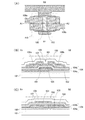
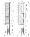
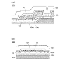
図1(A)は、チャネルが形成される半導体層に酸化物半導体を用いたトランジスタ15
0の平面構成を示す上面図であり、図1(B)は、図1(A)中でA1−A2の鎖線で示
した部位の断面構成を示す断面図であり、図1(C)は、図1(A)中でB1−B2の鎖
線で示した部位の断面構成を示す断面図である。なお、図面をわかりやすくするため、図
1(A)において一部の構成要素の記載を省略している。
FIG. 1A illustrates a transistor 15 in which an oxide semiconductor is used for a semiconductor layer in which a channel is formed.
FIG. 1B is a cross-sectional view showing a cross-sectional structure of a portion indicated by a chain line A1-A2 in FIG. 1A, and FIG. FIG. 2 is a cross-sectional view showing a cross-sectional configuration of a portion indicated by a chain line B1-B2 in FIG. Note that some components are not illustrated in FIG. 1A for easy understanding of the drawing.
図1に示すトランジスタ150は、チャネルエッチング型と呼ばれるボトムゲート構造の
トランジスタの一つであり、また、逆スタガ型と呼ばれるトランジスタ構造の一つでもあ
る。
A
図1において、基板101上に絶縁層102が形成され、絶縁層102上にゲート電極1
03が形成され、ゲート電極103上にゲート絶縁層104が形成されている。図1では
、ゲート絶縁層104をゲート絶縁層104aとゲート絶縁層104bの積層とする例を
示しているが、ゲート絶縁層104は単層でもよいし、複数層の積層でもよい。
In FIG. 1, an insulating
03 is formed, and a
また、ゲート絶縁層104上に酸化物半導体層105が形成され、酸化物半導体層105
上にソース電極106a及びドレイン電極106bが形成されている。また、酸化物半導
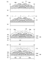
体層105の一部に接し、ソース電極106a及びドレイン電極106b上に絶縁層10
7が形成され、絶縁層107上に絶縁層108が形成されている。
In addition, an
A
7 is formed, and the insulating
酸化物半導体層105に用いる酸化物半導体としては、少なくともインジウム(In)あ
るいは亜鉛(Zn)を含むことが好ましい。特にInとZnを含むことが好ましい。また
、該酸化物半導体を用いたトランジスタの電気特性のばらつきを減らすためのスタビライ
ザーとして、それらに加えてガリウム(Ga)を有することが好ましい。また、スタビラ
イザーとしてスズ(Sn)を有することが好ましい。また、スタビライザーとしてハフニ
ウム(Hf)を有することが好ましい。また、スタビライザーとしてアルミニウム(Al
)を有することが好ましい。
An oxide semiconductor used for the
).
また、他のスタビライザーとして、ランタノイドである、ランタン(La)、セリウム(
Ce)、プラセオジム(Pr)、ネオジム(Nd)、サマリウム(Sm)、ユウロピウム
(Eu)、ガドリニウム(Gd)、テルビウム(Tb)、ジスプロシウム(Dy)、ホル
ミウム(Ho)、エルビウム(Er)、ツリウム(Tm)、イッテルビウム(Yb)、ル
テチウム(Lu)のいずれか一種あるいは複数種を有してもよい。
In addition, as other stabilizers, lanthanoids such as lanthanum (La), cerium (
Ce), praseodymium (Pr), neodymium (Nd), samarium (Sm), europium (Eu), gadolinium (Gd), terbium (Tb), dysprosium (Dy), holmium (Ho), erbium (Er), thulium ( Tm), ytterbium (Yb), or lutetium (Lu) may be used alone or in combination.
例えば、酸化物半導体として、酸化インジウム、酸化スズ、酸化亜鉛、二元系金属の酸化
物であるIn−Zn系酸化物、Sn−Zn系酸化物、Al−Zn系酸化物、Zn−Mg系
酸化物、Sn−Mg系酸化物、In−Mg系酸化物、In−Ga系酸化物、三元系金属の
酸化物であるIn−Ga−Zn系酸化物(IGZOとも表記する)、In−Al−Zn系
酸化物、In−Sn−Zn系酸化物、Sn−Ga−Zn系酸化物、Al−Ga−Zn系酸
化物、Sn−Al−Zn系酸化物、In−Hf−Zn系酸化物、In−La−Zn系酸化
物、In−Ce−Zn系酸化物、In−Pr−Zn系酸化物、In−Nd−Zn系酸化物
、In−Sm−Zn系酸化物、In−Eu−Zn系酸化物、In−Gd−Zn系酸化物、
In−Tb−Zn系酸化物、In−Dy−Zn系酸化物、In−Ho−Zn系酸化物、I
n−Er−Zn系酸化物、In−Tm−Zn系酸化物、In−Yb−Zn系酸化物、In
−Lu−Zn系酸化物、四元系金属の酸化物であるIn−Sn−Ga−Zn系酸化物、I
n−Hf−Ga−Zn系酸化物、In−Al−Ga−Zn系酸化物、In−Sn−Al−
Zn系酸化物、In−Sn−Hf−Zn系酸化物、In−Hf−Al−Zn系酸化物を用
いることができる。また、上記酸化物半導体にSiO2を含ませてもよい。
For example, as an oxide semiconductor, indium oxide, tin oxide, zinc oxide, binary metal oxides such as In—Zn oxide, Sn—Zn oxide, Al—Zn oxide, Zn—Mg oxide Oxides, Sn—Mg oxides, In—Mg oxides, In—Ga oxides, In—Ga—Zn oxides (also referred to as IGZO) which are oxides of ternary metals, In— Al-Zn oxide, In-Sn-Zn oxide, Sn-Ga-Zn oxide, Al-Ga-Zn oxide, Sn-Al-Zn oxide, In-Hf-Zn oxide In-La-Zn-based oxide, In-Ce-Zn-based oxide, In-Pr-Zn-based oxide, In-Nd-Zn-based oxide, In-Sm-Zn-based oxide, In-Eu -Zn-based oxide, In-Gd-Zn-based oxide,
In-Tb-Zn-based oxide, In-Dy-Zn-based oxide, In-Ho-Zn-based oxide, I
n-Er-Zn-based oxide, In-Tm-Zn-based oxide, In-Yb-Zn-based oxide, In
-Lu-Zn-based oxide, In-Sn-Ga-Zn-based oxide which is an oxide of a quaternary metal, I
n-Hf-Ga-Zn-based oxide, In-Al-Ga-Zn-based oxide, In-Sn-Al-
A Zn-based oxide, an In-Sn-Hf-Zn-based oxide, or an In-Hf-Al-Zn-based oxide can be used. In addition, SiO 2 may be included in the oxide semiconductor.
ここで、例えば、In−Ga−Zn系酸化物とは、インジウム(In)、ガリウム(Ga
)、亜鉛(Zn)を有する酸化物、という意味であり、InとGaとZnの比率は問わな
い。また、InとGaとZn以外の金属元素を含んでもよい。このとき、酸化物半導体の
化学量論比に対し、酸素を過剰にすると好ましい。酸素を過剰にすることで酸化物半導体
の酸素欠損に起因するキャリアの生成を抑制することができる。
Here, for example, an In—Ga—Zn-based oxide includes indium (In) and gallium (Ga
), An oxide having zinc (Zn), and the ratio of In, Ga, and Zn is not limited. Moreover, metal elements other than In, Ga, and Zn may be included. At this time, it is preferable that oxygen be excessive with respect to the stoichiometric ratio of the oxide semiconductor. When oxygen is excessive, generation of carriers due to oxygen vacancies in the oxide semiconductor can be suppressed.
また、酸化物半導体層は、化学式InMO3(ZnO)m(m>0)で表記される薄膜を
用いることができる。ここで、Mは、Sn、Zn、Ga、Al、Mn及びCoから選ばれ
た一の金属元素または複数の金属元素を示す。また、酸化物半導体として、In2SnO
5(ZnO)n(n>0)で表記される材料を用いてもよい。
As the oxide semiconductor layer, a thin film represented by the chemical formula, InMO 3 (ZnO) m (m> 0) can be used. Here, M represents one metal element or a plurality of metal elements selected from Sn, Zn, Ga, Al, Mn, and Co. As an oxide semiconductor, In 2 SnO
A material represented by 5 (ZnO) n (n> 0) may be used.
例えば、In:Ga:Zn=1:1:1(=1/3:1/3:1/3)あるいはIn:G
a:Zn=2:2:1(=2/5:2/5:1/5)の原子数比のIn−Ga−Zn系酸
化物やその組成の近傍の酸化物を用いることができる。あるいは、In:Sn:Zn=1
:1:1(=1/3:1/3:1/3)、In:Sn:Zn=2:1:3(=1/3:1
/6:1/2)あるいはIn:Sn:Zn=2:1:5(=1/4:1/8:5/8)の
原子数比のIn−Sn−Zn系酸化物やその組成の近傍の酸化物を用いるとよい。
For example, In: Ga: Zn = 1: 1: 1 (= 1/3: 1/3: 1/3) or In: G
An In—Ga—Zn-based oxide having an atomic ratio of a: Zn = 2: 2: 1 (= 2/5: 2/5: 1/5) or an oxide in the vicinity of the composition can be used. Or, In: Sn: Zn = 1
: 1: 1 (= 1/3: 1/3: 1/3), In: Sn: Zn = 2: 1: 3 (= 1/3: 1)
/ 6: 1/2) or In: Sn: Zn = 2: 1: 5 (= 1/4: 1/8: 5/8) atomic ratio In—Sn—Zn-based oxides and compositions thereof A nearby oxide may be used.
しかし、これらに限られず、必要とする半導体特性(移動度、しきい値、ばらつき等)に
応じて適切な組成のものを用いればよい。また、必要とする半導体特性を得るために、キ
ャリア濃度や不純物濃度、欠陥密度、金属元素と酸素の原子数比、原子間距離、密度等を
適切なものとすることが好ましい。
However, the composition is not limited thereto, and a material having an appropriate composition may be used depending on required semiconductor characteristics (mobility, threshold value, variation, etc.). In order to obtain the required semiconductor characteristics, it is preferable that the carrier concentration, the impurity concentration, the defect density, the atomic ratio between the metal element and oxygen, the interatomic distance, the density, and the like are appropriate.
例えば、In−Sn−Zn系酸化物では比較的容易に高い移動度が得られる。しかしなが
ら、In−Ga−Zn系酸化物でも、バルク内欠陥密度を低減することにより移動度を上
げることができる。
For example, high mobility can be obtained relatively easily with an In—Sn—Zn-based oxide. However, mobility can be increased by reducing the defect density in the bulk also in the case of using an In—Ga—Zn-based oxide.
なお、例えば、In、Ga、Znの原子数比がIn:Ga:Zn=a:b:c(a+b+
c=1)である酸化物と、原子数比がIn:Ga:Zn=A:B:C(A+B+C=1)
の酸化物の組成が近傍であるとは、a、b、cが、
(a―A)2+(b―B)2+(c―C)2≦r2
を満たすことを言い、rは、例えば、0.05とすればよい。他の酸化物でも同様である
。
For example, the atomic ratio of In, Ga, and Zn is In: Ga: Zn = a: b: c (a + b +
c = 1) and an atomic ratio of In: Ga: Zn = A: B: C (A + B + C = 1).
The composition of the oxide is in the vicinity of a, b, c,
(A−A) 2 + (b−B) 2 + (c−C) 2 ≦ r 2
R may be 0.05, for example. The same applies to other oxides.
酸化物半導体膜は、例えば非単結晶を有してもよい。非単結晶は、例えば、CAAC(C
Axis Aligned Crystal)、多結晶、微結晶、非晶質部を有する。
非晶質部は、微結晶、CAACよりも欠陥準位密度が高い。また、微結晶は、CAACよ
りも欠陥準位密度が高い。なお、CAACを有する酸化物半導体を、CAAC−OS(C
Axis Aligned Crystalline Oxide Semicond
uctor)と呼ぶ。
For example, the oxide semiconductor film may include a non-single crystal. Non-single crystals are, for example, CAAC (C
(Axis Aligned Crystal), polycrystalline, microcrystalline, and amorphous part.
The amorphous part has a higher density of defect states than microcrystals and CAAC. In addition, microcrystals have a higher density of defect states than CAAC. Note that an CAAC-OS (C
Axis Aligned Crystalline Oxide Semiconductor
uctor).
非晶質(アモルファス)状態の酸化物半導体膜は、比較的容易に平坦な表面を得ることが
できるため、これを用いてトランジスタを作製した際の界面散乱を低減でき、比較的容易
に、比較的高い移動度を得ることができる。
Since an oxide semiconductor film in an amorphous state can obtain a flat surface relatively easily, interface scattering when a transistor is manufactured using the oxide semiconductor film can be reduced. High mobility can be obtained.
また、結晶性を有する酸化物半導体膜では、よりバルク内欠陥を低減することができ、表
面の平坦性を高めればアモルファス状態の酸化物半導体膜以上の移動度を得ることができ
る。表面の平坦性を高めるためには、平坦な表面上に酸化物半導体膜を形成することが好
ましく、具体的には、平均面粗さ(Ra)が1nm以下、好ましくは0.3nm以下、よ
り好ましくは0.1nm以下の表面上に形成するとよい。なお、Raは原子間力顕微鏡(
AFM:Atomic Force Microscope)にて評価可能である。
In addition, in an oxide semiconductor film having crystallinity, defects in a bulk can be further reduced, and mobility higher than that of an oxide semiconductor film in an amorphous state can be obtained by increasing surface flatness. In order to enhance the flatness of the surface, it is preferable to form an oxide semiconductor film over the flat surface. Specifically, the average surface roughness (Ra) is 1 nm or less, preferably 0.3 nm or less. Preferably it is good to form on the surface below 0.1nm. Ra is an atomic force microscope (
Evaluation is possible with AFM (Atomic Force Microscope).
また、酸化物半導体膜としてIn−Zn系酸化物の材料を用いる場合、原子数比で、In
/Zn=0.5以上50以下、好ましくはIn/Zn=1以上20以下、さらに好ましく
はIn/Zn=1.5以上15以下とする。Znの原子数比を好ましい前記範囲とするこ
とで、トランジスタの電界効果移動度を向上させることができる。ここで、化合物の原子
数比がIn:Zn:O=X:Y:Zのとき、Z>1.5X+Yとする。
In the case where an In—Zn-based oxide material is used for the oxide semiconductor film, the atomic ratio is In.
/Zn=0.5 to 50, preferably In / Zn = 1 to 20 and more preferably In / Zn = 1.5 to 15. By setting the atomic ratio of Zn within the preferable range, the field effect mobility of the transistor can be improved. Here, when the atomic ratio of the compound is In: Zn: O = X: Y: Z, Z> 1.5X + Y.
酸化物半導体膜は、例えばCAAC−OSを有してもよい。CAAC−OSは、例えば、
c軸配向し、a軸または/およびb軸はマクロに揃っていない。
For example, the oxide semiconductor film may include a CAAC-OS. The CAAC-OS is, for example,
c-axis oriented, and the a-axis and / or b-axis are not aligned macroscopically.
酸化物半導体膜は、例えば微結晶を有してもよい。なお、微結晶を有する酸化物半導体を
、微結晶酸化物半導体と呼ぶ。微結晶酸化物半導体膜は、例えば、1nm以上10nm未
満のサイズの微結晶(ナノ結晶ともいう。)を膜中に含む。または、微結晶酸化物半導体
膜は、例えば、1nm以上10nm未満の結晶部を有する結晶−非晶質混相構造の酸化物
半導体を有している。
The oxide semiconductor film may include microcrystal, for example. Note that an oxide semiconductor including microcrystal is referred to as a microcrystalline oxide semiconductor. The microcrystalline oxide semiconductor film includes microcrystal (also referred to as nanocrystal) with a size greater than or equal to 1 nm and less than 10 nm, for example. Alternatively, the microcrystalline oxide semiconductor film includes an oxide semiconductor having a crystal-amorphous mixed phase structure with a crystal part of 1 nm to less than 10 nm, for example.
酸化物半導体膜は、例えば非晶質部を有してもよい。なお、非晶質部を有する酸化物半導
体を、非晶質酸化物半導体と呼ぶ。非晶質酸化物半導体膜は、例えば、原子配列が無秩序
であり、結晶成分を有さない。または、非晶質酸化物半導体膜は、例えば、完全な非晶質
であり、結晶部を有さない。
For example, the oxide semiconductor film may include an amorphous part. Note that an oxide semiconductor having an amorphous part is referred to as an amorphous oxide semiconductor. An amorphous oxide semiconductor film has, for example, disordered atomic arrangement and no crystal component. Alternatively, the amorphous oxide semiconductor film is, for example, completely amorphous and has no crystal part.
なお、酸化物半導体膜が、CAAC−OS、微結晶酸化物半導体、非晶質酸化物半導体の
混合膜であってもよい。混合膜は、例えば、非晶質酸化物半導体の領域と、微結晶酸化物
半導体の領域と、CAAC−OSの領域と、を有する。また、混合膜は、例えば、非晶質
酸化物半導体の領域と、微結晶酸化物半導体の領域と、CAAC−OSの領域と、の積層
構造を有してもよい。
Note that the oxide semiconductor film may be a mixed film of a CAAC-OS, a microcrystalline oxide semiconductor, and an amorphous oxide semiconductor. For example, the mixed film includes an amorphous oxide semiconductor region, a microcrystalline oxide semiconductor region, and a CAAC-OS region. The mixed film may have a stacked structure of an amorphous oxide semiconductor region, a microcrystalline oxide semiconductor region, and a CAAC-OS region, for example.
なお、酸化物半導体膜は、例えば、単結晶を有してもよい。 Note that the oxide semiconductor film may include a single crystal, for example.
酸化物半導体膜は、複数の結晶部を有し、当該結晶部のc軸が被形成面の法線ベクトルま
たは表面の法線ベクトルに平行な方向に揃っていることが好ましい。なお、異なる結晶部
間で、それぞれa軸およびb軸の向きが異なっていてもよい。そのような酸化物半導体膜
の一例としては、CAAC−OS膜がある。
The oxide semiconductor film preferably includes a plurality of crystal parts, and the c-axis of the crystal parts is aligned in a direction parallel to the normal vector of the formation surface or the normal vector of the surface. Note that the directions of the a-axis and the b-axis may be different between different crystal parts. An example of such an oxide semiconductor film is a CAAC-OS film.
CAAC−OS膜は、完全な非晶質ではない。CAAC−OS膜は、例えば、結晶部およ
び非晶質部を有する結晶−非晶質混相構造の酸化物半導体を有している。なお、当該結晶
部は、一辺が100nm未満の立方体内に収まる大きさであることが多い。また、透過型
電子顕微鏡(TEM:Transmission Electron Microsco
pe)による観察像では、CAAC−OS膜に含まれる非晶質部と結晶部との境界、結晶
部と結晶部との境界は明確ではない。また、TEMによってCAAC−OS膜には粒界(
グレインバウンダリーともいう。)は確認できない。そのため、CAAC−OS膜は、粒
界に起因する電子移動度の低下が抑制される。
The CAAC-OS film is not completely amorphous. The CAAC-OS film includes, for example, an oxide semiconductor with a crystal-amorphous mixed phase structure including a crystal part and an amorphous part. Note that the crystal part is often large enough to fit in a cube whose one side is less than 100 nm. In addition, transmission electron microscope (TEM: Transmission Electron Microsco)
In the observation image by pe), the boundary between the amorphous part and the crystal part and the boundary between the crystal part and the crystal part included in the CAAC-OS film are not clear. Further, the grain boundary (on the CAAC-OS film by TEM (
Also called grain boundary. ) Cannot be confirmed. Therefore, in the CAAC-OS film, reduction in electron mobility due to grain boundaries is suppressed.
CAAC−OS膜に含まれる結晶部は、c軸がCAAC−OS膜の被形成面の法線ベクト
ルまたは表面の法線ベクトルに平行な方向に揃い、かつab面に垂直な方向から見て三角
形状または六角形状の原子配列を有し、c軸に垂直な方向から見て金属原子が層状または
金属原子と酸素原子とが層状に配列している。なお、異なる結晶部間で、それぞれa軸お
よびb軸の向きが異なっていてもよい。本明細書において、単に垂直と記載する場合、8
0°以上100°以下、好ましくは85°以上95°以下の範囲が含まれることとする。
また、単に平行と記載する場合、−10°以上10°以下、好ましくは−5°以上5°以
下の範囲が含まれることとする。
In the crystal part included in the CAAC-OS film, the c-axis is aligned in a direction parallel to the normal vector of the formation surface of the CAAC-OS film or the normal vector of the surface, and triangular when viewed from the direction perpendicular to the ab plane. It has a shape or hexagonal atomic arrangement, and metal atoms are arranged in layers or metal atoms and oxygen atoms are arranged in layers as viewed from the direction perpendicular to the c-axis. Note that the directions of the a-axis and the b-axis may be different between different crystal parts. In the present specification, when simply described as vertical, 8
A range of 0 ° to 100 °, preferably 85 ° to 95 ° is included.
In addition, a simple term “parallel” includes a range of −10 ° to 10 °, preferably −5 ° to 5 °.
なお、CAAC−OS膜において、結晶部の分布が一様でなくてもよい。例えば、CAA
C−OS膜の形成過程において、酸化物半導体膜の表面側から結晶成長させる場合、被形
成面の近傍に対し表面の近傍では結晶部の占める割合が高くなることがある。また、CA
AC−OS膜へ不純物を添加することにより、当該不純物添加領域において結晶部が非晶
質化することもある。
Note that the distribution of crystal parts in the CAAC-OS film is not necessarily uniform. For example, CAA
In the formation process of the C-OS film, when crystal growth is performed from the surface side of the oxide semiconductor film, the ratio of crystal parts in the vicinity of the surface of the oxide semiconductor film may be higher in the vicinity of the surface. CA
When an impurity is added to the AC-OS film, the crystal part in a region to which the impurity is added becomes amorphous in some cases.
CAAC−OS膜に含まれる結晶部のc軸は、CAAC−OS膜の被形成面の法線ベクト
ルまたは表面の法線ベクトルに平行な方向に揃うため、CAAC−OS膜の形状(被形成
面の断面形状または表面の断面形状)によっては互いに異なる方向を向くことがある。ま
た、結晶部は、成膜したとき、または成膜後に加熱処理などの結晶化処理を行ったときに
形成される。従って、結晶部のc軸の方向は、CAAC−OS膜が形成されたときの被形
成面の法線ベクトルまたは表面の法線ベクトルに平行な方向になるように揃う。
Since the c-axis of the crystal part included in the CAAC-OS film is aligned in a direction parallel to the normal vector of the formation surface of the CAAC-OS film or the normal vector of the surface, the shape of the CAAC-OS film (formation surface) Depending on the cross-sectional shape of the surface or the cross-sectional shape of the surface). The crystal part is formed when a film is formed or when a crystallization process such as a heat treatment is performed after the film formation. Therefore, the c-axis direction of the crystal part is aligned so as to be parallel to the normal vector of the surface where the CAAC-OS film is formed or the normal vector of the surface.
CAAC−OS膜を用いたトランジスタは、可視光や紫外光の照射による電気特性の変動
が小さい。よって、当該トランジスタは、信頼性が高い。
In a transistor using a CAAC-OS film, change in electrical characteristics due to irradiation with visible light or ultraviolet light is small. Therefore, the transistor has high reliability.
なお、酸化物半導体を構成する酸素の一部は窒素で置換されてもよい。 Note that part of oxygen included in the oxide semiconductor may be replaced with nitrogen.
また、CAAC−OSのように結晶部を有する酸化物半導体では、よりバルク内欠陥を低
減することができ、表面の平坦性を高めればアモルファス状態の酸化物半導体以上の移動
度を得ることができる。表面の平坦性を高めるためには、平坦な表面上に酸化物半導体を
形成することが好ましく、具体的には、平均面粗さ(Ra)が1nm以下、好ましくは0
.3nm以下、より好ましくは0.1nm以下の表面上に形成するとよい。Raは原子間
力顕微鏡(AFM:Atomic Force Microscope)にて評価可能で
ある。
Further, in an oxide semiconductor having a crystal part such as a CAAC-OS, defects in a bulk can be further reduced, and mobility higher than that of an oxide semiconductor in an amorphous state can be obtained by increasing surface flatness. . In order to improve the flatness of the surface, it is preferable to form an oxide semiconductor on the flat surface. Specifically, the average surface roughness (Ra) is 1 nm or less, preferably 0.
. It may be formed on the surface of 3 nm or less, more preferably 0.1 nm or less. Ra can be evaluated with an atomic force microscope (AFM).
ただし、本実施の形態で説明するトランジスタ150は、ボトムゲート型であるため、酸
化物半導体膜の下方には、ゲート電極103とゲート絶縁層104が存在している。従っ
て、上記平坦な表面を得るために基板上にゲート電極103及びゲート絶縁層104を形
成した後、少なくともゲート電極103と重畳するゲート絶縁層104の表面に対して化
学的機械研磨(CMP:Chemical Mechanical Polishing
)処理などの平坦化処理を行ってもよい。
However, since the
) A flattening process such as a process may be performed.
酸化物半導体層105の厚さは、1nm以上30nm以下(好ましくは5nm以上10n
m以下)とし、スパッタリング法、MBE(Molecular Beam Epita
xy)法、CVD法、パルスレーザ堆積法、ALD(Atomic Layer Dep
osition)法等を適宜用いることができる。また、酸化物半導体層105は、スパ
ッタリングターゲット表面に対し、概略垂直に複数の基板表面がセットされた状態で成膜
を行うスパッタ装置を用いて成膜してもよい。
The thickness of the
m or less), sputtering method, MBE (Molecular Beam Epita)
xy) method, CVD method, pulsed laser deposition method, ALD (Atomic Layer Dep)
osition) method or the like can be used as appropriate. Alternatively, the
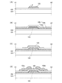
続いて、トランジスタ150の作製方法の一例を、図2及び図3を用いて説明する。
Next, an example of a method for manufacturing the
まず、基板101上に絶縁層102を形成し、絶縁層102上にゲート電極103を形成
する(図2(A)参照)。基板101に使用することができる基板に大きな制限はないが
、少なくとも、後の熱処理に耐えうる程度の耐熱性を有していることが必要となる。例え
ば、ガラス基板、セラミック基板、シリコンや炭化シリコンなどの単結晶半導体基板また
は多結晶半導体基板、シリコンゲルマニウムなどの化合物半導体基板、SOI基板の他、
本作製工程の処理温度に耐えうる程度の耐熱性を有するプラスチック基板等を用いること
ができる。また、これらの基板上に半導体素子が設けられたものを、基板101として用
いてもよい。
First, the insulating
A plastic substrate or the like having heat resistance high enough to withstand the processing temperature in this manufacturing process can be used. A substrate in which a semiconductor element is provided over these substrates may be used as the
ガラス基板としては、例えば、バリウムホウケイ酸ガラス、アルミノホウケイ酸ガラスま
たはアルミノケイ酸ガラス等の無アルカリガラス基板を用いるとよい。他に、石英基板、
サファイア基板などを用いることができる。また、基板101として、可撓性基板(フレ
キシブル基板)を用いてもよい。可撓性基板を用いる場合、可撓性基板上に、トランジス
タ150を直接作製してもよいし、他の作製基板上にトランジスタ150を作製し、その
後可撓性基板に剥離、転置してもよい。なお、作製基板から可撓性基板に剥離、転置する
ために、作製基板とトランジスタとの間に、剥離層を設けるとよい。本実施の形態では、
基板101として、アルミノホウケイ酸ガラスを用いる。
As the glass substrate, for example, an alkali-free glass substrate such as barium borosilicate glass, aluminoborosilicate glass, or aluminosilicate glass may be used. Besides, quartz substrate,
A sapphire substrate or the like can be used. Further, a flexible substrate (flexible substrate) may be used as the
As the
絶縁層102は下地層として機能し、基板101からの不純物元素の拡散を防止または低
減することができる。絶縁層102は、窒化アルミニウム、酸化アルミニウム、窒化酸化
アルミニウム、酸化窒化アルミニウム、酸化ガリウム、窒化シリコン、酸化シリコン、窒
化酸化シリコンまたは酸化窒化シリコンから選ばれた材料を、単層でまたは積層して形成
する。なお、本明細書中において、窒化酸化とは、その組成として、酸素よりも窒素の含
有量が多いものであって、酸化窒化とは、その組成として、窒素よりも酸素の含有量が多
いものを示す。なお、各元素の含有量は、例えば、ラザフォード後方散乱法(RBS:R
utherford Backscattering Spectrometry)等を
用いて測定することができる。絶縁層102は、スパッタリング法、CVD法、塗布法、
印刷法等を用いて形成することができる。
The insulating
It is possible to measure using, for example, a user backscattering spectroscopy. The insulating
It can be formed using a printing method or the like.
また、絶縁層102に、塩素、フッ素などのハロゲン元素を含ませることで、基板101
からの不純物元素の拡散を防止または低減する機能をさらに高めることができる。絶縁層
102に含ませるハロゲン元素の濃度は、二次イオン質量分析法(SIMS:Secon
dary Ion Mass Spectrometry)を用いた分析により得られる
濃度ピークにおいて、1×10¹⁵/cm3以上1×1020/cm3以下とすればよい
。
In addition, by including a halogen element such as chlorine or fluorine in the insulating
The function of preventing or reducing the diffusion of impurity elements from can be further enhanced. The concentration of the halogen element contained in the insulating
A concentration peak obtained by analysis using a dary Ion Mass Spectrometry may be 1 × 10 15 / cm 3 or more and 1 × 10 20 / cm 3 or less.
本実施の形態では、基板101上に絶縁層102としてプラズマCVD法を用いて膜厚2
00nmの酸化窒化シリコンを形成する。また、絶縁層102形成時の温度は、基板10
1が耐えうる温度以下で、より高いほうが好ましい。例えば、基板101を350℃以上
450℃以下の温度に加熱しながら絶縁層102を形成する。なお、絶縁層102形成時
の温度は一定であることが好ましい。例えば、絶縁層102の形成を、基板を350℃に
加熱して行う。
In this embodiment mode, a film thickness of 2 is formed using the plasma CVD method as the insulating
00 nm silicon oxynitride is formed. The temperature at which the insulating
It is preferable that the temperature is lower than the temperature 1 can withstand and higher. For example, the insulating
また、絶縁層102の形成後、減圧下、窒素雰囲気下、希ガス雰囲気下、または超乾燥エ
ア窒素雰囲気下において、加熱処理を行ってもよい。加熱処理により絶縁層102に含ま
れる水素、水分、水素化物、または水酸化物などの濃度を低減することができる。加熱処
理温度は、基板101が耐えうる温度以下で、より高い温度で行うことが好ましい。具体
的には、絶縁層102の成膜温度以上、基板101の歪点未満で行うことが好ましい。
Further, after the insulating
また、絶縁層102の形成後、絶縁層102に酸素ドープ処理を行い、絶縁層102を酸
素過剰な状態としてもよい。なお、絶縁層102への酸素ドープ処理は、上記加熱処理後
に行うことが好ましい。
Alternatively, after the insulating
次に、スパッタリング法、真空蒸着法、またはメッキ法を用いて後にゲート電極103と
なる導電層を形成する。ゲート電極103となる導電層は、アルミニウム(Al)、クロ
ム(Cr)、銅(Cu)、タンタル(Ta)、チタン(Ti)、モリブデン(Mo)、タ
ングステン(W)、ネオジム(Nd)、スカンジウム(Sc)から選ばれた金属元素、上
述した金属元素を成分とする合金、上述した金属元素を組み合わせた合金、上述した金属
元素の窒化物などを用いて形成することができる。また、マンガン(Mn)、マグネシウ
ム(Mg)、ジルコニウム(Zr)、ベリリウム(Be)のいずれか一または複数から選
択された金属元素を含む材料用いてもよい。また、リン等の不純物元素を含有させた多結
晶シリコンに代表される半導体、ニッケルシリサイドなどのシリサイドを用いてもよい。
Next, a conductive layer to be the
また、ゲート電極103となる導電層は、単層構造でも、二層以上の積層構造としてもよ
い。例えば、シリコンを含むアルミニウムを用いた単層構造、アルミニウム上にチタンを
積層する二層構造、窒化チタン上にチタンを積層する二層構造、窒化チタン上にタングス
テンを積層する二層構造、窒化タンタル上にタングステンを積層する二層構造、Cu−M
g−Al合金上にCuを積層する二層構造、窒化チタン上に銅を積層し、さらにその上に
タングステンを形成する三層構造などがある。
The conductive layer to be the
There are a two-layer structure in which Cu is laminated on a g-Al alloy, a three-layer structure in which copper is laminated on titanium nitride, and tungsten is further formed thereon.
また、ゲート電極103となる導電層は、インジウム錫酸化物、酸化タングステンを含む
インジウム酸化物、酸化タングステンを含むインジウム亜鉛酸化物、酸化チタンを含むイ
ンジウム酸化物、酸化チタンを含むインジウム錫酸化物、インジウム亜鉛酸化物、酸化ケ
イ素を添加したインジウム錫酸化物などの透光性を有する導電性材料を適用することもで
きる。また、上記透光性を有する導電性材料と、上記金属元素を含む材料の積層構造とす
ることもできる。
The conductive layer to be the
また、ゲート電極103となる導電層として、窒素を含む金属酸化物、具体的には、窒素
を含むIn−Ga−Zn系酸化物や、窒素を含むIn−Sn系酸化物や、窒素を含むIn
−Ga系酸化物や、窒素を含むIn−Zn系酸化物や、窒素を含むSn系酸化物や、窒素
を含むIn系酸化物や、金属窒化膜(InN、SnNなど)を用いることができる。
The conductive layer to be the
-Ga-based oxides, nitrogen-containing In-Zn-based oxides, nitrogen-containing Sn-based oxides, nitrogen-containing In-based oxides, and metal nitride films (InN, SnN, and the like) can be used. .
これらの材料は5eV(電子ボルト)以上の仕事関数を有し、ゲート電極として用いた場
合、トランジスタのしきい値電圧をプラスにすることができ、所謂ノーマリーオフのn型
トランジスタを実現できる。
These materials have a work function of 5 eV (electron volt) or more, and when used as a gate electrode, the threshold voltage of the transistor can be positive, so that a so-called normally-off n-type transistor can be realized.
本実施の形態では、ゲート電極103となる導電層として、スパッタリング法により厚さ
100nmのタングステンを形成する。
In this embodiment mode, tungsten with a thickness of 100 nm is formed by a sputtering method as the conductive layer to be the
次に、ゲート電極103となる導電層の一部を選択的にエッチングして、ゲート電極10
3(これと同じ層で形成される配線を含む)を形成する。導電層の一部を選択的にエッチ
ングする場合は、導電層上にレジストマスクを形成し、ドライエッチング法またはウェッ
トエッチング法により、導電層の不要部分を除去すればよい。また、導電層のエッチング
を、ドライエッチング法とウェットエッチング法の両方を組み合わせて行ってもよい。導
電層上に形成するレジストマスクはフォトリソグラフィ法、印刷法、インクジェット法等
を適宜用いることができる。レジストマスクをインクジェット法で形成するとフォトマス
クを使用しないため、製造コストを低減できる。
Next, a part of the conductive layer to be the
3 (including wiring formed in the same layer as this) is formed. In the case where a part of the conductive layer is selectively etched, a resist mask is formed over the conductive layer, and an unnecessary part of the conductive layer may be removed by a dry etching method or a wet etching method. In addition, the conductive layer may be etched by combining both dry etching and wet etching. As a resist mask formed over the conductive layer, a photolithography method, a printing method, an inkjet method, or the like can be used as appropriate. When the resist mask is formed by an ink-jet method, a manufacturing cost can be reduced because a photomask is not used.
導電層のエッチングをドライエッチング法で行う場合は、エッチングガスとしてハロゲン
元素を含むガスを用いることができる。ハロゲン元素を含むガスの一例としては、塩素(
Cl2)、三塩化硼素(BCl3)、四塩化珪素(SiCl4)もしくは四塩化炭素(C
Cl4)などを代表とする塩素系ガス、四フッ化炭素(CF4)、六フッ化硫黄(SF6
)、三フッ化窒素(NF3)もしくはトリフルオロメタン(CHF3)などを代表とする
フッ素系ガス、臭化水素(HBr)または酸素を適宜用いることができる。また用いるエ
ッチング用ガスに不活性気体を添加してもよい。また、ドライエッチング法としては、反
応性イオンエッチング(RIE:Reactive Ion Etching)法を用い
ることができる。
In the case where the conductive layer is etched by a dry etching method, a gas containing a halogen element can be used as an etching gas. An example of a gas containing a halogen element is chlorine (
Cl 2 ), boron trichloride (BCl 3 ), silicon tetrachloride (SiCl 4 ) or carbon tetrachloride (C
Cl 4 ) and other representative gases, carbon tetrafluoride (CF 4 ), sulfur hexafluoride (SF 6 )
), Nitrogen trifluoride (NF 3 ), trifluoromethane (CHF 3 ) or the like as a representative fluorine-based gas, hydrogen bromide (HBr), or oxygen can be used as appropriate. Further, an inert gas may be added to the etching gas used. As a dry etching method, a reactive ion etching (RIE) method can be used.
また、プラズマ源として、容量結合型プラズマ(CCP:Capacitively C
oupled Plasma)、誘導結合プラズマ(ICP:Inductively
Coupled Plasma)、電子サイクロトロン共鳴(ECR:Electron
Cyclotron Resonance)プラズマ、ヘリコン波励起プラズマ(HW
P:Helicon Wave Plasma)、マイクロ波励起表面波プラズマ(SW
P:Surface Wave Plasma)などを用いることができる。特に、IC
P、ECR、HWP、及びSWPは、高密度のプラズマを生成することができる。ドライ
エッチング法で行うエッチング(以下、「ドライエッチング処理」ともいう)は、所望の
加工形状にエッチングできるように、エッチング条件(コイル型の電極に印加される電力
量、基板側の電極に印加される電力量、基板側の電極温度等)を適宜調節して行う。
As a plasma source, capacitively coupled plasma (CCP: Capacitive C)
coupled plasma) (ICP: Inductively)
Coupled Plasma), Electron Cyclotron Resonance (ECR)
Cyclotron Resonance) plasma, helicon wave excited plasma (HW)
P: Helicon Wave Plasma), microwave excited surface wave plasma (SW
P: Surface Wave Plasma) or the like can be used. In particular, IC
P, ECR, HWP, and SWP can generate a high density plasma. Etching performed by a dry etching method (hereinafter also referred to as “dry etching treatment”) is performed under etching conditions (the amount of electric power applied to the coil-type electrode and the electrode on the substrate side so that etching into a desired processing shape can be performed. The amount of electric power to be generated, the electrode temperature on the substrate side, etc.) are adjusted as appropriate.
なお、フォトリソグラフィ法を用いて導電層や絶縁層上に任意形状のレジストマスクを形
成する工程をフォトリソグラフィ工程というが、一般にレジストマスク形成後には、エッ
チング工程とレジストマスクの剥離工程が行われることが多い。このため、特段の説明が
無い限り、本明細書でいうフォトリソグラフィ工程には、レジストマスクの形成工程と、
導電層または絶縁層のエッチング工程と、レジストマスクの剥離工程が含まれているもの
とする。
Note that a process of forming a resist mask having an arbitrary shape on a conductive layer or an insulating layer using a photolithography method is referred to as a photolithography process. Generally, after a resist mask is formed, an etching process and a resist mask peeling process are performed. There are many. Therefore, unless otherwise specified, the photolithography process referred to in this specification includes a resist mask forming process,
It is assumed that a conductive layer or insulating layer etching step and a resist mask peeling step are included.
また、ゲート電極103の断面形状、具体的には端部の断面形状(テーパー角や膜厚など
)を工夫することにより、ゲート電極103上に形成される層の被覆性を向上させること
ができる。
Further, by devising the cross-sectional shape of the
具体的には、ゲート電極103の断面形状が台形または三角形状となるように、ゲート電
極103の端部をテーパー形状とする。ここで、ゲート電極103端部のテーパー角θを
、60°以下、好ましくは45°以下、さらに好ましくは30°以下とする。このような
角度範囲とすることで、高いゲート電圧がゲート電極103に印加される場合、ソース電
極106a又はドレイン電極106bの端部近傍に生じる恐れのある電界集中を緩和する
ことができる。なお、テーパー角θとは、テーパー形状を有する層を、その断面(基板の
表面と直交する面)方向から観察した際に、当該層の側面と底面がなす当該層内の角度を
示す。また、テーパー角が90°未満である場合を順テーパーといい、テーパー角が90
°以上である場合を逆テーパーという。なお、ゲート電極103に限らず、各層の端部を
順テーパー形状とすることで、その上に被覆する層が途切れてしまう現象(段切れ)を防
ぎ、被覆性を良好なものとすることができる。
Specifically, the end portion of the
The case where it is more than ° is called reverse taper. Note that not only the
次いで、ゲート電極103上にゲート絶縁層104を形成する(図2(B)参照)。
Next, the
なお、ゲート絶縁層104の被覆性を向上させるために、ゲート電極103表面に平坦化
処理を行ってもよい。特にゲート絶縁層104として膜厚の薄い絶縁層を用いる場合、ゲ
ート電極103表面の平坦性が良好であることが好ましい。
Note that planarization treatment may be performed on the surface of the
ゲート絶縁層104は、スパッタリング法、MBE法、CVD法、パルスレーザ堆積法、
ALD法等を適宜用いて形成することができる。また、μ波(例えば周波数2.45GH
z)を用いた高密度プラズマCVD法などを適用することができる。また、ゲート絶縁層
104は、スパッタリングターゲット表面に対し、概略垂直に複数の基板表面がセットさ
れた状態で成膜を行うスパッタ装置を用いて成膜してもよい。
The
An ALD method or the like can be used as appropriate. In addition, μ-wave (for example, frequency 2.45GH
A high-density plasma CVD method using z) can be applied. Alternatively, the
ゲート絶縁層104の材料としては、窒化アルミニウム、酸化アルミニウム、窒化酸化ア
ルミニウム、酸化窒化アルミニウム、酸化ガリウム、窒化シリコン、酸化シリコン、窒化
酸化シリコンまたは酸化窒化シリコンから選ばれた材料を、単層でまたは積層して形成す
ることができる。本実施の形態では、ゲート絶縁層104として、ゲート絶縁層104a
とゲート絶縁層104bの積層を用いる。
As a material of the
And a stack of the
また、一般に、容量素子は対向する二つの電極の間に誘電体を挟む構成を有し、誘電体の
厚さが薄いほど(対向する二つの電極間距離が短いほど)、また、誘電体の誘電率が大き
いほど容量値が大きくなる。ただし、容量素子の容量値を増やすために誘電体を薄くする
と、二つの電極間に生じるリーク電流が増加しやすくなり、また、容量素子の絶縁耐圧が
低下しやすくなる。
In general, the capacitive element has a configuration in which a dielectric is sandwiched between two opposing electrodes. The thinner the dielectric (the shorter the distance between the two opposing electrodes), the more the dielectric As the dielectric constant increases, the capacitance value increases. However, if the dielectric is made thin in order to increase the capacitance value of the capacitive element, the leakage current generated between the two electrodes tends to increase, and the withstand voltage of the capacitive element tends to decrease.
トランジスタのゲート電極、ゲート絶縁層、半導体層が重畳する部分は、前述した容量素
子として機能する(以下、「ゲート容量」ともいう)。なお、半導体層の、ゲート絶縁層
を介してゲート電極と重畳する領域にチャネルが形成される。すなわち、ゲート電極と、
チャネル形成領域が容量素子の二つの電極として機能し、ゲート絶縁層が容量素子の誘電
体として機能する。ゲート容量の容量値は大きいほうが好ましいが、容量値を増やすため
にゲート絶縁層を薄くすると、前述のリーク電流の増加や、絶縁耐圧の低下といった問題
が生じやすい。
A portion where the gate electrode, the gate insulating layer, and the semiconductor layer of the transistor overlap functions as the above-described capacitor (hereinafter also referred to as “gate capacitor”). Note that a channel is formed in the semiconductor layer in a region overlapping with the gate electrode with the gate insulating layer interposed therebetween. That is, a gate electrode,
The channel formation region functions as two electrodes of the capacitor, and the gate insulating layer functions as a dielectric of the capacitor. Although it is preferable that the capacitance value of the gate capacitance is large, if the gate insulating layer is thinned in order to increase the capacitance value, problems such as an increase in the leakage current and a decrease in the withstand voltage are likely to occur.
そこで、ゲート絶縁層104として、ハフニウムシリケート(HfSixOy(x>0、
y>0))、窒素が添加されたハフニウムシリケート(HfSixOyNz(x>0、y
>0、z>0))、窒素が添加されたハフニウムアルミネート(HfAlxOyNz(x
>0、y>0、z>0))、酸化ハフニウム、酸化イットリウムなどのhigh−k材料
を用いると、ゲート絶縁層104を厚くしても、ゲート電極103と酸化物半導体層10
5間の容量値を十分確保することが可能となる。
Therefore, as the
y> 0)), nitrogen-added hafnium silicate (HfSi x O y N z (x> 0, y
> 0, z> 0)), and hafnium aluminate (HfAl x O y N z (x
> 0, y> 0, z> 0)), when a high-k material such as hafnium oxide or yttrium oxide is used, the
It is possible to ensure a sufficient capacitance value between 5.
例えば、ゲート絶縁層104として誘電率が大きいhigh−k材料を用いると、ゲート
絶縁層104を厚くしても、ゲート絶縁層104に酸化シリコンを用いた場合と同等の容
量値を実現できるため、ゲート電極103と酸化物半導体層105間に生じるリーク電流
を低減できる。また、ゲート電極103と同じ層を用いて形成された配線と、該配線と重
畳する他の配線との間に生じるリーク電流を低減できる。なお、ゲート絶縁層104をh
igh−k材料と、上記材料との積層構造としてもよい。
For example, when a high-k material having a high dielectric constant is used for the
A stacked structure of an i-k material and the above material may be used.
ゲート絶縁層104は、後に形成される酸化物半導体層105と接する部分において酸素
を含むことが好ましい。本実施の形態においては、酸化物半導体層105と接するゲート
絶縁層104bは、膜中(バルク中)に少なくとも化学量論比を超える量の酸素が存在す
ることが好ましい。例えば、ゲート絶縁層104bとして、酸化シリコン膜を用いる場合
には、SiO2+α(ただし、α>0)とする。この酸化シリコン膜をゲート絶縁層10
4bとして用いることで、酸化物半導体層105に酸素を供給することができ、特性を良
好にすることができる。
The
By using it as 4b, oxygen can be supplied to the
ゲート絶縁層104aは、窒化シリコンや酸化アルミニウムなどの、水素、水分、水素化
物、または水酸化物などの不純物や、酸素に対するバリア性を有する材料を用いることが
好ましい。ゲート絶縁層104aを、バリア性を有する材料で形成することで、基板側か
らの上記不純物の侵入を防ぐとともに、ゲート絶縁層104b中に含まれる酸素の基板側
への拡散を防ぐことができる。なお、ゲート絶縁層104としてバリア性を有する材料を
用いることで、下地層として機能する絶縁層102の形成を省略することもできる。
The
また、ゲート絶縁層104を形成する前に、酸素、一酸化二窒素、もしくは希ガス(代表
的にはアルゴン)などを用いたプラズマ処理により、被形成面の表面に付着した水分や有
機物などの不純物を除去することが好ましい。
Further, before the
また、ゲート絶縁層104の形成後、減圧下、窒素雰囲気下、希ガス雰囲気下、または超
乾燥エア窒素雰囲気下において、加熱処理を行ってもよい。加熱処理によりゲート絶縁層
104に含まれる水素、水分、水素化物、または水酸化物などの濃度を低減することがで
きる。加熱処理度は、基板101が耐えうる温度以下で、より高い温度で行うことが好ま
しい。具体的には、ゲート絶縁層104の成膜温度以上、基板101の歪点未満で行うこ
とが好ましい。
Further, after the
また、ゲート絶縁層104の形成後、ゲート絶縁層104に酸素ドープ処理を行い、ゲー
ト絶縁層104を酸素過剰な状態としてもよい。酸素ドープ処理は、イオン注入法、イオ
ンドーピング法、プラズマイマージョンイオンインプランテーション法、酸素雰囲気下で
行うプラズマ処理などを用いて行うことができる。なお、ゲート絶縁層104への酸素ド
ープ処理は、上記加熱処理後に行うことが好ましい。
Alternatively, after the
酸素の供給源となる酸素を多く(過剰に)含むゲート絶縁層104を酸化物半導体層10
5と接して設けることによって、その後の熱処理により該ゲート絶縁層104から酸化物
半導体層105へ酸素を供給することができる。
The
5 is provided so that oxygen can be supplied from the
酸化物半導体層105へ酸素を供給することにより、酸化物半導体層105中の酸素欠損
を補填することができる。さらに、ゲート絶縁層104は、作製するトランジスタのサイ
ズやゲート電極103への段差被覆性を考慮して形成することが好ましい。
By supplying oxygen to the
次に、ゲート絶縁層104(ゲート絶縁層104b)上に、後に酸化物半導体層105と
なる酸化物半導体層115(図示せず)をスパッタリング法により形成する。
Next, an oxide semiconductor layer 115 (not illustrated) which will be the
また、酸化物半導体層115の形成に先立ち、ゲート絶縁層104の酸化物半導体層10
5が接して形成される領域に、平坦化処理を行ってもよい。平坦化処理としては、特に限
定されないが、研磨処理(例えば、CMP処理)、ドライエッチング処理、プラズマ処理
を用いることができる。
Prior to the formation of the oxide semiconductor layer 115, the oxide semiconductor layer 10 of the
A planarization process may be performed on a region formed in contact with 5. The planarization treatment is not particularly limited, and polishing treatment (for example, CMP treatment), dry etching treatment, and plasma treatment can be used.
プラズマ処理としては、例えば、アルゴンガスを導入してプラズマを発生させる逆スパッ
タリングを行うことができる。逆スパッタリングとは、アルゴン雰囲気下で基板側にRF
電源を用いて電圧を印加して基板近傍にプラズマを形成して表面を改質する方法である。
なお、アルゴン雰囲気に代えて窒素、ヘリウム、酸素などを用いてもよい。逆スパッタリ
ングを行うと、ゲート絶縁層104の表面に付着している粉状物質(パーティクル、ごみ
ともいう)を除去することができる。
As the plasma treatment, for example, reverse sputtering in which an argon gas is introduced to generate plasma can be performed. Reverse sputtering is RF on the substrate side in an argon atmosphere.
In this method, a voltage is applied using a power source to form plasma in the vicinity of the substrate to modify the surface.
Note that nitrogen, helium, oxygen, or the like may be used instead of the argon atmosphere. When reverse sputtering is performed, powdery substances (also referred to as particles or dust) attached to the surface of the
また、平坦化処理としての、研磨処理、ドライエッチング処理、プラズマ処理は複数回行
ってもよく、それらを組み合わせて行ってもよい。また、組み合わせて行う場合、工程順
も特に限定されず、ゲート絶縁層104表面の凹凸状態に合わせて適宜設定すればよい。
Further, the polishing treatment, the dry etching treatment, and the plasma treatment as the planarization treatment may be performed a plurality of times, or may be performed in combination. In the case of performing the combination, the order of steps is not particularly limited, and may be set as appropriate depending on the uneven state of the surface of the
なお、酸化物半導体層115を形成するためのスパッタリングガスは、希ガス(代表的に
はアルゴン)雰囲気、酸素ガス雰囲気、希ガス及び酸素の混合ガスを適宜用いる。また、
スパッタリングガスには、水素、水、水酸基または水素化物などの不純物が除去された高
純度ガスを用いることが好ましい。
Note that as a sputtering gas for forming the oxide semiconductor layer 115, a rare gas (typically argon) atmosphere, an oxygen gas atmosphere, or a mixed gas of a rare gas and oxygen is used as appropriate. Also,
As the sputtering gas, it is preferable to use a high-purity gas from which impurities such as hydrogen, water, a hydroxyl group, or hydride are removed.
なお、酸化物半導体層115は、酸素が多く含まれるような条件(例えば、酸素100%
の雰囲気下でスパッタリング法により成膜を行うなど)で形成して、酸素を多く含むまた
は酸素が過飽和な状態(好ましくは酸化物半導体が結晶状態における化学量論的組成に対
し、酸素の含有量が過剰な領域が含まれている状態)とすることが好ましい。
Note that the oxide semiconductor layer 115 is formed under a condition that contains a large amount of oxygen (for example, oxygen 100%
The oxygen content is higher than that in the stoichiometric composition in which the oxide semiconductor contains a large amount of oxygen or is supersaturated (preferably the oxide semiconductor is in a crystalline state). Is a state in which an excessive region is included).
例えば、スパッタリング法を用いて酸化物半導体層を形成する場合、スパッタリングガス
の酸素の占める割合が多い条件で行うことが好ましく、スパッタリングガスを酸素ガス1
00%として行うことが好ましい。スパッタリングガス中の酸素ガスの占める割合が多い
条件、特に酸素ガス100%で成膜すると、例えば形成温度を300℃以上としても、酸
化物半導体層中からのZnの放出が抑えられる。
For example, in the case where an oxide semiconductor layer is formed by a sputtering method, the sputtering gas is preferably used under a condition where the proportion of oxygen in the sputtering gas is large.
It is preferable to carry out as 00%. When a film is formed under a condition where the proportion of oxygen gas in the sputtering gas is large, particularly 100% oxygen gas, release of Zn from the oxide semiconductor layer can be suppressed even when the formation temperature is 300 ° C. or higher, for example.
また、酸化物半導体層115は、銅、アルミニウム、塩素などの不純物がほとんど含まれ
ない高純度化されたものであることが望ましい。トランジスタの製造工程において、これ
らの不純物が混入または酸化物半導体層表面に付着する恐れのない工程を適宜選択するこ
とが好ましい。具体的には、酸化物半導体層中の銅濃度は1×10¹⁸atoms/cm
3以下、好ましくは1×10¹⁷atoms/cm3以下とする。また、酸化物半導体層
中のアルミニウム濃度は1×10¹⁸atoms/cm3以下とする。また、酸化物半導
体層中の塩素濃度は2×10¹⁸atoms/cm3以下とする。
In addition, the oxide semiconductor layer 115 is preferably a highly purified layer that hardly contains impurities such as copper, aluminum, and chlorine. In the manufacturing process of the transistor, it is preferable to select as appropriate a process in which these impurities are not mixed or attached to the surface of the oxide semiconductor layer. Specifically, the copper concentration in the oxide semiconductor layer is 1 × 10 18 atoms / cm.
3 or less, preferably 1 × 10 17 atoms / cm 3 or less. The aluminum concentration in the oxide semiconductor layer is 1 × 10 18 atoms / cm 3 or less. The chlorine concentration in the oxide semiconductor layer is 2 × 10 18 atoms / cm 3 or less.
また、酸化物半導体層115中のナトリウム(Na)、リチウム(Li)、カリウム(K
)などのアルカリ金属の濃度は、Naは5×1016cm−3以下、好ましくは1×10
16cm−3以下、さらに好ましくは1×1015cm−3以下、Liは5×10¹⁵c
m−3以下、好ましくは1×1015cm−3以下、Kは5×1015cm−3以下、好
ましくは1×1015cm−3以下とする。
In addition, sodium (Na), lithium (Li), potassium (K in the oxide semiconductor layer 115 is used.
) And the like, the concentration of Na is 5 × 10 16 cm −3 or less, preferably 1 × 10
16 cm −3 or less, more preferably 1 × 10 15 cm −3 or less, Li is 5 × 10 15 c
m −3 or less, preferably 1 × 10 15 cm −3 or less, and K is 5 × 10 15 cm −3 or less, preferably 1 × 10 15 cm −3 or less.
本実施の形態においては、酸化物半導体層115として、AC電源装置を有するスパッタ
リング装置を用いたスパッタリング法により、膜厚35nmのIn−Ga−Zn系酸化物
(IGZO)を形成する。スパッタリング法で作製するためのターゲットとしては、組成
として、In:Ga:Zn=1:1:1[原子数比]の金属酸化物ターゲットを用いる。
In this embodiment, as the oxide semiconductor layer 115, an In—Ga—Zn-based oxide (IGZO) with a thickness of 35 nm is formed by a sputtering method using a sputtering apparatus having an AC power supply device. As a target for manufacturing by a sputtering method, a metal oxide target of In: Ga: Zn = 1: 1: 1 [atomic ratio] is used as a composition.
また、金属酸化物ターゲットの相対密度(充填率)は90%以上100%以下、好ましく
は95%以上99.9%以下である。相対密度の高い金属酸化物ターゲットを用いること
により、成膜した酸化物半導体層は緻密な層とすることができる。
The relative density (filling rate) of the metal oxide target is 90% to 100%, preferably 95% to 99.9%. By using a metal oxide target with a high relative density, the formed oxide semiconductor layer can be a dense layer.
まず、減圧状態に保持された成膜室内に基板101を保持する。そして、成膜室内の残留
水分を除去しつつ水素及び水分が除去されたスパッタガスを導入し、上記ターゲットを用
いてゲート絶縁層104上に酸化物半導体層115を形成する。成膜室内の残留水分を除
去するためには、吸着型の真空ポンプ、例えば、クライオポンプ、イオンポンプ、チタン
サブリメーションポンプを用いることが好ましい。また、排気手段としては、ターボ分子
ポンプにコールドトラップを加えたものであってもよい。クライオポンプを用いて排気し
た成膜室は、例えば、水素原子、水(H2O)など水素原子を含む化合物(より好ましく
は炭素原子を含む化合物も)等が排気されるため、当該成膜室で形成した酸化物半導体層
115に含まれる不純物の濃度を低減できる。
First, the
また、ゲート絶縁層104と酸化物半導体層115を大気に解放せずに連続的に形成して
もよい。ゲート絶縁層104と酸化物半導体層115とを大気に曝露せずに連続して形成
すると、ゲート絶縁層104表面に水素や水分などの不純物が付着することを防止するこ
とができる。
Alternatively, the
次に、フォトリソグラフィ工程を用いて、酸化物半導体層115の一部を選択的にエッチ
ングし、島状の酸化物半導体層105を形成する(図2(C)参照)。また、酸化物半導
体層105を形成するためのレジストマスクをインクジェット法で形成してもよい。レジ
ストマスクをインクジェット法で形成するとフォトマスクを使用しないため、製造コスト
を低減できる。
Next, part of the oxide semiconductor layer 115 is selectively etched using a photolithography step, so that the island-shaped
なお、酸化物半導体層115のエッチングは、ドライエッチング法でもウェットエッチン
グ法でもよく、両方を用いてもよい。ウェットエッチング法により、酸化物半導体層11
5のエッチングを行う場合は、エッチング液として、燐酸と酢酸と硝酸を混ぜた溶液や、
シュウ酸を含む溶液などを用いることができる。また、ITO−07N(関東化学社製)
を用いてもよい。また、ドライエッチング法で酸化物半導体層115のエッチングを行う
場合は、例えば、ECR(Electron Cyclotron Resonance
)またはICP(Inductively Coupled Plasma)などの高密
度プラズマ源を用いたドライエッチング法を用いることができる。また、広い面積に渡っ
て一様な放電が得られやすいドライエッチング法として、ECCP(Enhanced
Capacitively Coupled Plasma)モードを用いたドライエッ
チング法がある。このドライエッチング法であれば、例えば基板として、第10世代の3
mを超えるサイズの基板を用いる場合にも対応することができる。
Note that the oxide semiconductor layer 115 may be etched by a dry etching method or a wet etching method, or both of them may be used. The oxide semiconductor layer 11 is formed by wet etching.
When etching 5 is performed, as an etchant, a mixed solution of phosphoric acid, acetic acid and nitric acid,
A solution containing oxalic acid can be used. ITO-07N (manufactured by Kanto Chemical Co., Inc.)
May be used. In the case where the oxide semiconductor layer 115 is etched by a dry etching method, for example, ECR (Electron Cyclotron Resonance) is used.
) Or ICP (Inductively Coupled Plasma) or the like, a dry etching method using a high-density plasma source can be used. In addition, ECCP (Enhanced) is used as a dry etching method in which uniform discharge can be easily obtained over a wide area.
There is a dry etching method using a Capacitively Coupled Plasma) mode. With this dry etching method, for example, as a substrate, the 10th generation 3
It is possible to cope with the case of using a substrate having a size exceeding m.
また、酸化物半導体層105形成後に、酸化物半導体層105中の過剰な水素(水や水酸
基を含む)を除去(脱水化または脱水素化)するための加熱処理を行ってもよい。加熱処
理の温度は、300℃以上700℃以下、または基板の歪み点未満とする。加熱処理は減
圧下又は窒素雰囲気下などで行うことができる。例えば、加熱処理装置の一つである電気
炉に基板を導入し、酸化物半導体層105に対して窒素雰囲気下450℃において1時間
の加熱処理を行う。
Further, after the
なお、加熱処理装置は電気炉に限られず、抵抗発熱体などの発熱体からの熱伝導または熱
輻射によって、被処理物を加熱する装置を用いてもよい。例えば、GRTA(Gas R
apid Thermal Anneal)装置、LRTA(Lamp Rapid T
hermal Anneal)装置等のRTA(Rapid Thermal Anne
al)装置を用いることができる。LRTA装置は、ハロゲンランプ、メタルハライドラ
ンプ、キセノンアークランプ、カーボンアークランプ、高圧ナトリウムランプ、高圧水銀
ランプなどのランプから発する光(電磁波)の輻射により、被処理物を加熱する装置であ
る。GRTA装置は、高温のガスを用いて加熱処理を行う装置である。高温のガスには、
アルゴンなどの希ガス、または窒素のような、加熱処理によって被処理物と反応しない不
活性気体が用いられる。
Note that the heat treatment apparatus is not limited to an electric furnace, and an apparatus for heating an object to be processed by heat conduction or heat radiation from a heating element such as a resistance heating element may be used. For example, GRTA (Gas R
API (Temperature Annial), LRTA (Lamp Rapid T)
RTA (Rapid Thermal Anne) such as a Herm Anneal) device
al) apparatus can be used. The LRTA apparatus is an apparatus that heats an object to be processed by radiation of light (electromagnetic waves) emitted from a lamp such as a halogen lamp, a metal halide lamp, a xenon arc lamp, a carbon arc lamp, a high pressure sodium lamp, or a high pressure mercury lamp. The GRTA apparatus is an apparatus that performs heat treatment using a high-temperature gas. For hot gases,
An inert gas that does not react with an object to be processed by heat treatment, such as nitrogen or a rare gas such as argon, is used.
例えば、加熱処理として、650℃〜700℃の高温に加熱した不活性ガス中に基板を入
れ、数分間加熱した後、基板を不活性ガス中から出すGRTAを行ってもよい。
For example, as the heat treatment, GRTA may be performed in which the substrate is placed in an inert gas heated to a high temperature of 650 ° C. to 700 ° C., heated for several minutes, and then the substrate is taken out of the inert gas.
なお、加熱処理においては、窒素、またはヘリウム、ネオン、アルゴン等の希ガスに、水
、水素などが含まれないことが好ましい。または、熱処理装置に導入する窒素、またはヘ
リウム、ネオン、アルゴン等の希ガスの純度を、6N(99.9999%)以上好ましく
は7N(99.99999%)以上(即ち不純物濃度を1ppm以下、好ましくは0.1
ppm以下)とすることが好ましい。
Note that in the heat treatment, it is preferable that water, hydrogen, or the like be not contained in nitrogen or a rare gas such as helium, neon, or argon. Alternatively, the purity of nitrogen or a rare gas such as helium, neon, or argon introduced into the heat treatment apparatus is 6N (99.9999%) or more, preferably 7N (99.99999%) or more (that is, the impurity concentration is 1 ppm or less, preferably Is 0.1
ppm or less).
また、加熱処理により酸化物半導体層105を加熱した後、同じ炉に高純度の酸素ガス、
高純度の一酸化二窒素ガス、又は超乾燥エア(キャビティリングダウン分光法(CRDS
:Cavity Ring−Down Spectroscopy)を用いた露点計を用
いて測定した場合の水分量が20ppm(露点換算で−55℃)以下、好ましくは1pp
m以下、より好ましくは10ppb以下の空気)を導入してもよい。酸素ガスまたは一酸
化二窒素ガスに、水、水素などが含まれないことが好ましい。または、熱処理装置に導入
する酸素ガスまたは一酸化二窒素ガスの純度を、6N以上好ましくは7N以上(即ち、酸
素ガスまたは一酸化二窒素ガス中の不純物濃度を1ppm以下、好ましくは0.1ppm
以下)とすることが好ましい。酸素ガス又は一酸化二窒素ガスの作用により、脱水化また
は脱水素化処理による不純物の排除工程によって同時に減少してしまった酸化物半導体を
構成する主成分材料である酸素を供給することによって、酸化物半導体内の酸素欠損が低
減され、酸化物半導体層105をi型(真性)または実質的にi型化することができる。
この点、シリコンなどのように不純物元素を添加してのi型化ではないため、酸化物半導
体のi型化は従来にない技術思想を含むものといえる。
In addition, after the
High purity dinitrogen monoxide gas or ultra dry air (Cavity Ring Down Spectroscopy (CRDS
: Water content when measured using a dew point meter using Cavity Ring-Down Spectroscopy (20 ° C. in terms of dew point) or less, preferably 1 pp
m or less, more preferably 10 ppb or less air) may be introduced. It is preferable that water, hydrogen, and the like are not contained in the oxygen gas or the dinitrogen monoxide gas. Alternatively, the purity of the oxygen gas or nitrous oxide introduced into the heat treatment apparatus is 6N or more, preferably 7N or more (that is, the impurity concentration in the oxygen gas or nitrous oxide is 1 ppm or less, preferably 0.1 ppm).
Or less). Oxygen is supplied by supplying oxygen, which is a main component material of the oxide semiconductor, which has been reduced by the process of removing impurities by dehydration or dehydrogenation treatment by the action of oxygen gas or dinitrogen monoxide gas. Oxygen vacancies in the physical semiconductor are reduced, and the
In this respect, since it is not i-type by adding an impurity element such as silicon, it can be said that i-type oxide semiconductor includes an unprecedented technical idea.
脱水化又は脱水素化のための加熱処理は、酸化物半導体層の形成後であれば、島状の酸化
物半導体層105の形成前に行ってもよく、形成後に行ってもよい。また、脱水化又は脱
水素化のための加熱処理は、複数回行ってもよく、他の加熱処理と兼ねてもよい。
The heat treatment for dehydration or dehydrogenation may be performed before or after the formation of the island-shaped
また、脱水化又は脱水素化処理によって、酸化物半導体を構成する主成分材料である酸素
が同時に脱離して減少してしまう恐れがある。酸化物半導体層において、酸素が脱離した
箇所では酸素欠損が存在し、該酸素欠損に起因してトランジスタの電気特性変動を招くド
ナー準位が生じてしまう。
Further, oxygen that is a main component material of the oxide semiconductor may be desorbed and reduced at the same time by dehydration or dehydrogenation treatment. In the oxide semiconductor layer, oxygen vacancies exist in portions where oxygen is released, and donor levels that cause fluctuations in electric characteristics of the transistor are generated due to the oxygen vacancies.
このため、脱水化又は脱水素化処理を行った酸化物半導体層105に、酸素ドープ処理を
行い、酸化物半導体層105中に酸素を供給してもよい。
Therefore, oxygen doping treatment may be performed on the
脱水化又は脱水素化処理を行った酸化物半導体層105に、酸素を導入して酸化物半導体
層105中に酸素を供給することによって、脱水化または脱水素化処理による不純物の排
除工程によって生じた酸化物半導体内の酸素欠損を低減し、酸化物半導体層105をi型
(真性)化することができる。i型(真性)化した酸化物半導体層105を有するトラン
ジスタは、電気特性変動が抑制されており、電気的に安定である。
Oxygen is introduced into the
酸化物半導体層105に酸素導入する場合、酸素ドープ処理を酸化物半導体層105に直
接行ってもよいし、他の層を介して行ってもよい。
In the case of introducing oxygen into the
また、酸素の導入により、酸化物半導体層105を構成する元素と水素の間の結合、或い
は該元素と水酸基の間の結合を切断するとともに、これらの水素または水酸基が酸素と反
応することで水を生成するため、酸素の導入後に加熱処理を行うと、不純物である水素ま
たは水酸基が、水として脱離しやすくなる。このため、酸化物半導体層105へ酸素を導
入した後に加熱処理を行ってもよい。その後、さらに酸化物半導体層105に酸素を導入
し、酸化物半導体層105を酸素過剰な状態としてもよい。また、酸化物半導体層105
への酸素の導入と加熱処理は、それぞれを交互に複数回行ってもよい。また、加熱処理と
酸素の導入を同時に行ってもよい。
In addition, by introducing oxygen, a bond between an element included in the
The introduction of oxygen and the heat treatment may be alternately performed a plurality of times. Further, heat treatment and oxygen introduction may be performed at the same time.
このように、酸化物半導体層105は水素などの不純物が十分に除去されることにより高
純度化され、また、十分な酸素が供給されて酸化物半導体層105中の酸素欠損が低減さ
れることにより、i型(真性)または実質的にi型(真性)化されたものであることが望
ましい。
As described above, the
電子供与体(ドナー)となる水分または水素などの不純物が低減されて高純度化された酸
化物半導体(purified OS)は、その後、酸化物半導体に酸素を供給して、酸
化物半導体内の酸素欠損を低減することによりi型(真性)の酸化物半導体又はi型に限
りなく近い(実質的にi型化した)酸化物半導体とすることができる。チャネルが形成さ
れる半導体層にi型または実質的にi型化された酸化物半導体を用いたトランジスタは、
オフ電流が著しく低いという特性を有する。
An oxide semiconductor (purified OS), which is purified by reducing impurities such as moisture or hydrogen, which serves as an electron donor (donor), supplies oxygen to the oxide semiconductor, and then oxygen in the oxide semiconductor. By reducing defects, an i-type (intrinsic) oxide semiconductor or an oxide semiconductor that is almost as close to i-type (substantially i-type) can be obtained. A transistor using an i-type or substantially i-type oxide semiconductor for a semiconductor layer in which a channel is formed is
It has a characteristic that the off-state current is extremely low.
具体的に、高純度化された酸化物半導体層の水素濃度は、SIMSによる水素濃度の測定
値が、好ましくは5×10¹⁹atoms/cm3以下、より好ましくは5×1018a
toms/cm3以下、さらにより好ましくは5×1017atoms/cm3以下とす
る。また、酸化物半導体層105に十分な酸素が供給されて酸素が過飽和の状態とするた
め、酸化物半導体層105を挟むように酸素を多く含む絶縁層(酸化シリコンなど)を接
して設けることが好ましい。
Specifically, as for the hydrogen concentration of the highly purified oxide semiconductor layer, the measured value of the hydrogen concentration by SIMS is preferably 5 × 10 19 atoms / cm 3 or less, more preferably 5 × 10 18 a.
toms / cm 3 or less, more preferably 5 × 10 17 atoms / cm 3 or less. In addition, since sufficient oxygen is supplied to the
また、酸素を多く含む絶縁層の水素濃度もトランジスタの特性に影響を与えるため重要で
ある。酸素を多く含む絶縁層の水素濃度が、7.2×10²⁰atoms/cm3以上で
ある場合には、トランジスタの初期特性のバラツキの増大、L長依存性の増大、さらにB
Tストレス試験において大きく劣化するため、酸素を多く含む絶縁層の水素濃度は、好ま
しくは7.2×10²⁰atoms/cm3未満とする。即ち、酸化物半導体層の水素濃
度は5×10¹⁹atoms/cm3以下、且つ、酸素を多く含む絶縁層の水素濃度は、
7.2×10²⁰atoms/cm3未満とすることが好ましい。
Further, the hydrogen concentration in the insulating layer containing a large amount of oxygen is also important because it affects the characteristics of the transistor. When the hydrogen concentration of the insulating layer containing a large amount of oxygen is 7.2 × 10 20 atoms / cm 3 or more, variation in initial characteristics of the transistor increases, dependency on L length increases, and B
The hydrogen concentration of the insulating layer containing a large amount of oxygen is preferably less than 7.2 × 10 20 atoms / cm 3 because it greatly deteriorates in the T stress test. That is, the hydrogen concentration of the oxide semiconductor layer is 5 × 10 19 atoms / cm 3 or less, and the hydrogen concentration of the insulating layer containing a large amount of oxygen is
It is preferable to be less than 7.2 × 10 20 atoms / cm 3 .
ここで、水素濃度のSIMS分析について触れておく。SIMS分析は、その原理上、試
料表面近傍や、材質が異なる膜との積層界面近傍のデータを正確に得ることが困難である
ことが知られている。そこで、層中における水素濃度の厚さ方向の分布をSIMSで分析
する場合、対象となる層が存在する範囲において、値に極端な変動が無く、ほぼ一定の値
が得られる領域における平均値を、水素濃度として採用する。また、測定の対象となる層
の厚さが小さい場合、隣接する膜内の水素濃度の影響を受けて、ほぼ一定の値が得られる
領域を見いだせない場合がある。この場合、当該層が存在する領域における、水素濃度の
最大値または最小値を、当該層中の水素濃度として採用する。さらに、当該層が存在する
領域において、最大値を有する山型のピーク、最小値を有する谷型のピークが存在しない
場合、変曲点の値を水素濃度として採用する。
Here, the SIMS analysis of the hydrogen concentration is mentioned. In SIMS analysis, it is known that, based on the principle, it is difficult to accurately obtain data in the vicinity of the sample surface and in the vicinity of the laminated interface with films of different materials. Therefore, when analyzing the distribution of the hydrogen concentration in the layer in the thickness direction by SIMS, the average value in a region where there is no extreme variation in the value and an almost constant value can be obtained in the range where the target layer exists. Adopted as hydrogen concentration. In addition, when the thickness of the layer to be measured is small, there may be a case where an area where a substantially constant value is obtained cannot be found due to the influence of the hydrogen concentration in the adjacent film. In this case, the maximum value or the minimum value of the hydrogen concentration in the region where the layer exists is adopted as the hydrogen concentration in the layer. Furthermore, in the region where the layer is present, when there is no peak peak having the maximum value and no valley peak having the minimum value, the value of the inflection point is adopted as the hydrogen concentration.
次いで、酸化物半導体層105上に導電層117(図示せず)を形成し、フォトリソグラ
フィ工程により導電層117の一部を選択的にエッチングして、ソース電極106a及び
ドレイン電極106bを形成する(図2(D)参照)。
Next, a conductive layer 117 (not illustrated) is formed over the
ソース電極106a及びドレイン電極106bとなる導電層117は、後の加熱処理に耐
えられる材料を用いて形成する。導電層117としては、例えば、Al、Cr、Cu、T
a、Ti、Mo、Wから選ばれた元素を含む金属、または上述した元素を成分とする金属
窒化物(窒化チタン、窒化モリブデン、窒化タングステン)等を用いることができる。ま
た、Al、Cuなどの金属層の下側又は上側の一方または双方にTi、Mo、Wなどの高
融点金属またはそれらの金属窒化物(窒化チタン、窒化モリブデン、窒化タングステン)
を積層させた構成としても良い。導電層117を導電性の金属酸化物で形成しても良い。
導電性の金属酸化物としては酸化インジウム(In2O3)、酸化スズ(SnO2)、酸
化亜鉛(ZnO)、酸化インジウム酸化スズ(In2O3―SnO2、ITOと略記する
)、酸化インジウム酸化亜鉛(In2O3―ZnO)またはこれらの金属酸化物材料に酸
化シリコンを含ませたものを用いることができる。
The conductive layer 117 to be the
A metal containing an element selected from a, Ti, Mo, and W, or a metal nitride (titanium nitride, molybdenum nitride, tungsten nitride) containing the above-described element as a component can be used. In addition, one or both of the lower side and the upper side of a metal layer such as Al or Cu, or a refractory metal such as Ti, Mo, or W or a metal nitride thereof (titanium nitride, molybdenum nitride, tungsten nitride)
It is good also as a structure which laminated | stacked. The conductive layer 117 may be formed using a conductive metal oxide.
Examples of the conductive metal oxide include indium oxide (In 2 O 3 ), tin oxide (SnO 2 ), zinc oxide (ZnO), indium tin oxide (In 2 O 3 —SnO 2 , abbreviated as ITO), oxidation Indium zinc oxide (In 2 O 3 —ZnO) or a metal oxide material containing silicon oxide can be used.
本実施の形態では、導電層117としてスパッタリング法により厚さ200nmのチタン
を形成する。導電層117のエッチングは、ゲート電極103の形成と同様の方法で行う
ことができる。例えば、エッチングガス(BCl3:Cl2=750sccm:150s
ccm)を用い、バイアス電力を1500Wとし、ICP電源電力を0Wとし、圧力を2
.0PaとしたICPエッチング法により行うことができる。
In this embodiment mode, titanium with a thickness of 200 nm is formed as the conductive layer 117 by a sputtering method. The conductive layer 117 can be etched by a method similar to that for forming the
ccm), the bias power is 1500 W, the ICP power supply power is 0 W, and the pressure is 2
. The ICP etching method can be performed at 0 Pa.
なお、ソース電極106a及びドレイン電極106bの形成により露出した酸化物半導体
層105の表面には、ソース電極106a及びドレイン電極106bを構成する元素や、
処理室内に存在する元素、エッチングに用いたエッチングガスを構成する元素が不純物と
して付着する場合がある。
Note that an element included in the
There are cases where elements existing in the processing chamber and elements constituting the etching gas used for etching adhere as impurities.
不純物が付着すると、トランジスタのオフ電流の増加、或いはトランジスタの電気特性の
劣化がもたらされやすい。また、酸化物半導体層105に寄生チャネルが生じやすくなり
、電気的に分離されるべき電極が酸化物半導体層105を介して電気的に接続されやすく
なる。
When impurities are attached, an increase in off-state current of the transistor or deterioration in electrical characteristics of the transistor is likely to occur. In addition, a parasitic channel is easily generated in the
また、不純物によっては、酸化物半導体層105内の表面近傍や側面近傍に混入し、酸化
物半導体層105中の酸素を引き抜いてしまい、酸化物半導体層105の表面近傍や側面
近傍に酸素欠損が形成されることがある。例えば、上述したエッチングガスに含まれる塩
素やボロンや、処理室の構成材料であるアルミニウムは、酸化物半導体層105がn型化
する要因の一つとなりうる。
Further, depending on impurities, the
そこで、本発明の一態様では、ソース電極106a及びドレイン電極106bを形成する
ためのエッチングが終了した後、酸化物半導体層105及びソース電極106a及びドレ
イン電極106bの表面や側面に付着した不純物を除去するための洗浄処理(不純物除去
処理)を行う。
Therefore, in one embodiment of the present invention, after the etching for forming the
不純物除去処理は、プラズマ処理、または溶液による処理によって行うことができる。プ
ラズマ処理としては、酸素プラズマ処理または一酸化二窒素プラズマ処理などを用いるこ
とができる。また、プラズマ処理として希ガス(代表的にはアルゴン)を用いてもよい。
The impurity removal treatment can be performed by plasma treatment or solution treatment. As the plasma treatment, oxygen plasma treatment, dinitrogen monoxide plasma treatment, or the like can be used. Further, a rare gas (typically argon) may be used for the plasma treatment.
また、溶液による洗浄処理としては、TMAH溶液などのアルカリ性の溶液、水、希フッ
酸などの酸性の溶液を用いて行うことができる。例えば、希フッ酸を用いる場合、50w
t%フッ酸を、水で1/102乃至1/105程度、好ましくは1/103乃至1/10
5程度に希釈した希フッ酸を使用する。すなわち、濃度が0.5重量%乃至5×10⁻⁴
重量%の希フッ酸、好ましくは5×10⁻²重量%乃至5×10⁻⁴重量%の希フッ酸を
洗浄処理に用いることが望ましい。洗浄処理により、露出した酸化物半導体層105の表
面に付着した上記不純物を除去することができる。
Further, the washing treatment with a solution can be performed using an alkaline solution such as a TMAH solution or an acidic solution such as water or dilute hydrofluoric acid. For example, when dilute hydrofluoric acid is used, 50w
t% hydrofluoric acid is about 1/10 2 to 1/10 5 with water, preferably 1/10 3 to 1/10.
Use dilute hydrofluoric acid diluted to about 5 . That is, the concentration is 0.5 wt% to 5 × 10 −4.
It is desirable to use dilute hydrofluoric acid in weight%, preferably 5 × 10 −2 wt% to 5 × 10 −4 wt% dilute hydrofluoric acid for the cleaning treatment. By the cleaning treatment, the impurities attached to the exposed surface of the
また、希フッ酸溶液を用いて不純物除去処理を行うと、露出した酸化物半導体層105の
表面をエッチングすることができる。すなわち、露出した酸化物半導体層105の表面に
付着した不純物や、酸化物半導体層105内の表面近傍に混入した不純物を、酸化物半導
体層105の一部とともに除去することができる。これにより、酸化物半導体層105に
おいて、ソース電極106a及びドレイン電極106bと重畳する領域の厚さが、ソース
電極106a及びドレイン電極106bと重畳しない領域の厚さより大きくなる。
Further, when impurity removal treatment is performed using a diluted hydrofluoric acid solution, the exposed surface of the
不純物除去処理を行うことで、SIMSを用いた分析により得られる濃度ピークにおいて
、酸化物半導体層表面における塩素濃度を1×10¹⁹/cm3以下(好ましくは5×1
018/cm3以下、さらに好ましくは1×1018/cm3以下)とすることができる
。また、ボロン濃度を1×10¹⁹/cm3以下(好ましくは5×1018/cm3以下
、さらに好ましくは1×10¹⁸/cm3以下)とすることができる。また、アルミニウ
ム濃度を1×10¹⁹/cm3以下(好ましくは5×1018/cm3以下、さらに好ま
しくは1×10¹⁸/cm3以下)とすることができる。
By performing the impurity removal treatment, the chlorine concentration on the surface of the oxide semiconductor layer is 1 × 10 19 / cm 3 or less (preferably 5 × 1) at the concentration peak obtained by the analysis using SIMS.
0 18 / cm 3 or less, more preferably 1 × 10 18 / cm 3 or less. Further, the boron concentration can be set to 1 × 10 19 / cm 3 or less (preferably 5 × 10 18 / cm 3 or less, more preferably 1 × 10 18 / cm 3 or less). In addition, the aluminum concentration can be set to 1 × 10 19 / cm 3 or less (preferably 5 × 10 18 / cm 3 or less, more preferably 1 × 10 18 / cm 3 or less).
不純物除去処理を行うことで、安定した電気特性を有する信頼性の高いトランジスタ15
0を実現することができる。
By performing the impurity removal treatment, the highly reliable transistor 15 having stable electrical characteristics.
0 can be realized.
次いで、酸化物半導体層105の一部に接し、ソース電極106a及びドレイン電極10
6b上に、酸化物半導体層105と接する絶縁層111を20nm乃至50nmの厚さで
形成する(図3(A)参照)。絶縁層111は、絶縁層102またはゲート絶縁層104
と同様の材料及び方法で形成することができる。例えば、酸化シリコンや、酸化窒化シリ
コンなどをスパッタリング法やCVD法で形成し、絶縁層107として用いることができ
る。
Next, the
An insulating
The same material and method can be used. For example, silicon oxide, silicon oxynitride, or the like can be formed by a sputtering method or a CVD method and used as the insulating
本実施の形態では、絶縁層111として、プラズマCVD法により厚さ30nmの酸化窒
化シリコンを形成する。絶縁層111の形成は、例えば、SiH4とN2Oのガス流量比
をSiH4:N2O=20sccm:3000sccmとし、圧力を40Paとし、RF
電源電力(電源出力)を100Wとし、基板温度を350℃とすればよい。
In this embodiment, as the insulating
The power source power (power output) may be 100 W and the substrate temperature may be 350 ° C.
次に、絶縁層111に酸素121を導入し、絶縁層111を、酸素を過剰に含む絶縁層1
07とする。(図3(B)参照)。酸素121には、少なくとも、酸素ラジカル、オゾン
、酸素原子、酸素イオン(分子イオン、クラスタイオンを含む)、のいずれかが含まれて
いる。酸素121の導入は、酸素ドープ処理により行うことができる。
Next,
07. (See FIG. 3B). The
また、酸素121の導入は、絶縁層111の全面を一度に処理してもよいし、例えば、線
状のイオンビームを用いてもよい。線状のイオンビームを用いる場合には、基板101又
はイオンビームを相対的に移動(スキャン)させることで、絶縁層111の全面に酸素1
21を導入することができる。
In addition, the introduction of the
21 can be introduced.
酸素121の供給ガスとしては、酸素原子を含有するガスを用いればよく、例えば、O2
ガス、N2Oガス、CO2ガス、COガス、NO2ガス等を用いることができる。なお、
酸素の供給ガスに希ガス(例えばAr)を含有させてもよい。
As a supply gas of the
Gas, N 2 O gas, CO 2 gas, CO gas, NO 2 gas, or the like can be used. In addition,
A rare gas (eg, Ar) may be included in the oxygen supply gas.
また、例えば、イオン注入法で酸素の導入を行う場合、酸素121のドーズ量は1×10
13ions/cm2以上5×1016ions/cm2以下とするのが好ましく、絶縁
層107の酸素の含有量は、化学量論的組成を超える程度とするのが好ましい。なお、こ
のような化学量論的組成よりも酸素を過剰に含む領域は、絶縁層107の一部に存在して
いればよい。なお、酸素の注入深さは、注入条件により適宜制御すればよい。
For example, when oxygen is introduced by an ion implantation method, the dose of
It is preferable to set it to 13 ions / cm 2 or more and 5 × 10 16 ions / cm 2 or less, and the content of oxygen in the insulating
本実施の形態では、酸素121の導入を、酸素雰囲気下で行うプラズマ処理で行う。なお
、絶縁層107は、酸化物半導体層105と接する絶縁層であるため、可能な限り水、水
素などの不純物が含まれないことが好ましい。したがって、酸素121の導入の前に、絶
縁層111中の水素(水や水酸基を含む)を低減するための加熱処理を行うことが好まし
い。脱水化又は脱水素化処理を目的とした加熱処理の温度は、300℃以上700℃以下
、または基板の歪み点未満とする。脱水化又は脱水素化処理を目的とした加熱処理は、前
述の加熱処理と同様に行うことができる。
In this embodiment mode, the
酸素121の導入のためのプラズマ処理(酸素プラズマ処理)は、酸素流量を250sc
cmとし、ICP電源電力を0Wとし、バイアス電力を4500Wとし、圧力を15Pa
として行う。この時、酸素プラズマ処理により絶縁層111に導入された酸素の一部は、
絶縁層111を通過して酸化物半導体層105に導入される。酸化物半導体層105中に
絶縁層111を介して酸素が導入されるため、酸化物半導体層105の表面にプラズマに
よるダメージが入りにくく、半導体装置の信頼性を向上することができる。絶縁層111
は、10nmより厚く、100nmより薄くすることが好ましい。絶縁層111の厚さを
10nm以下とすると、酸化物半導体層105が酸素プラズマ処理時のダメージを受けや
すくなる。また、絶縁層111の厚さを100nm以上とすると、酸素プラズマ処理によ
り導入された酸素が、十分に酸化物半導体層105に供給されない恐れがある。また、絶
縁層111の脱水化又は脱水素化処理を目的とした加熱処理及び/又は酸素121の導入
は、複数回行ってもよい。絶縁層111に酸素を導入することにより、絶縁層107を酸
素供給層として機能させることができる。
In the plasma treatment (oxygen plasma treatment) for introducing
cm, ICP power supply power 0 W, bias power 4500 W, pressure 15 Pa
Do as. At this time, a part of oxygen introduced into the insulating
The
Is preferably thicker than 10 nm and thinner than 100 nm. When the thickness of the insulating
次に、絶縁層107上に絶縁層108を200nm乃至500nmの厚さで形成する(図
3(C)参照)。絶縁層108は、絶縁層102またはゲート絶縁層104と同様の材料
及び方法で形成することができる。例えば、酸化シリコンや酸化窒化シリコンなどをスパ
ッタリング法やCVD法で形成し、絶縁層108として用いることができる。
Next, the insulating
本実施の形態では、絶縁層108として、プラズマCVD法により厚さ370nmの酸化
窒化シリコンを形成する。絶縁層108の形成は、例えば、SiH4とN2Oのガス流量
比をSiH4:N2O=30sccm:4000sccmとし、圧力を200Paとし、
RF電源電力(電源出力)を150Wとし、基板温度を220℃とすればよい。
In this embodiment, silicon oxynitride having a thickness of 370 nm is formed as the insulating
The RF power supply power (power output) may be 150 W and the substrate temperature may be 220 ° C.
なお、絶縁層108の形成後、不活性ガス雰囲気下、酸素雰囲気下、または不活性ガスと
酸素の混合雰囲気下で250℃以上650℃以下、好ましくは300℃以上600℃以下
の温度で加熱処理を行ってもよい。当該加熱処理によって、絶縁層107に含まれる酸素
を酸化物半導体層105へと供給し、酸化物半導体層105の酸素欠損を補填することが
できる。絶縁層107上に絶縁層108を形成することで、絶縁層107が含有する酸素
を効率良く酸化物半導体層105に供給することができる。
Note that after the insulating
また、絶縁層108に酸素ドープ処理を行い、絶縁層108に酸素121を導入し、酸素
過剰な状態としてもよい。絶縁層108への酸素121の導入は、絶縁層107への酸素
121の導入と同様に行ってもよい。また、絶縁層108への酸素121の導入後、不活
性ガス雰囲気下、酸素雰囲気下、または不活性ガスと酸素の混合雰囲気下で250℃以上
650℃以下、好ましくは300℃以上600℃以下の温度で加熱処理を行ってもよい。
Alternatively, oxygen insulation treatment may be performed on the insulating
図11(A)は、図1(B)に示す部位201の拡大図であり、図11(B)は、図1(
C)に示す部位202の拡大図である。図11(A)、図11(B)に示す矢印は、絶縁
層107に含まれる酸素122が酸化物半導体層105に供給される様子を示している。
絶縁層107に含まれる酸素122は、酸化物半導体層105と絶縁層107が接する領
域で酸化物半導体層105に直接供給されるだけでなく、ゲート絶縁層104bを介して
酸化物半導体層105に間接的にも供給される。また、絶縁層108またはゲート絶縁層
104bを酸素過剰な状態とした場合は、絶縁層108またはゲート絶縁層104bに含
まれる酸素も酸化物半導体層105に供給することができる。
FIG. 11A is an enlarged view of a
It is an enlarged view of the site |
The
以上の工程によって、本実施の形態のトランジスタ150が形成される。なお、トランジ
スタ150上にさらに絶縁層を形成してもかまわない。本実施の形態では、トランジスタ
150上に平坦化絶縁層110を形成する例を示す(図3(D)参照)。平坦化絶縁層1
10としては、ポリイミド、アクリル樹脂、ポリイミドアミド、べンゾシクロブテン系樹
脂、ポリアミド、エポキシ樹脂等の耐熱性を有する有機材料を用いることができる。また
、上記有機材料の他に、低誘電率材料(low−k材料)、シロキサン系樹脂、PSG(
リンガラス)、BPSG(リンボロンガラス)等を用いることができる。なお、これらの
材料で形成される絶縁層を複数積層させることで平坦化絶縁層110を形成してもよい。
Through the above process, the
As 10, an organic material having heat resistance such as polyimide, acrylic resin, polyimide amide, benzocyclobutene resin, polyamide, epoxy resin, or the like can be used. In addition to the above organic materials, low dielectric constant materials (low-k materials), siloxane resins, PSG (
(Phosphorus glass), BPSG (phosphorus boron glass), or the like can be used. Note that the
チャネルが形成される半導体層に酸化物半導体を用いたトランジスタは、酸化物半導体層
に酸素が供給されることで、酸化物半導体層と絶縁層との界面準位密度を低減できる。こ
の結果、トランジスタの動作などに起因して、酸化物半導体層と絶縁層との界面にキャリ
アが捕獲されることを抑制することができ、信頼性の高いトランジスタを得ることができ
る。
In a transistor in which an oxide semiconductor is used for a semiconductor layer in which a channel is formed, the interface state density between the oxide semiconductor layer and the insulating layer can be reduced by supplying oxygen to the oxide semiconductor layer. As a result, carriers can be prevented from being trapped at the interface between the oxide semiconductor layer and the insulating layer due to the operation of the transistor, and a highly reliable transistor can be obtained.
さらに、酸化物半導体層の酸素欠損に起因してキャリアが生じる場合がある。一般に酸化
物半導体層の酸素欠損は、酸化物半導体層中にキャリアである電子が生成される一因とな
る。この結果、トランジスタのしきい値電圧がマイナス方向にシフトしてしまう。そこで
、酸化物半導体層に酸素が十分に供給され、好ましくは酸化物半導体層に酸素が過剰に含
まれていることにより、酸化物半導体層の酸素欠損密度を低減することができる。
Further, carriers may be generated due to oxygen vacancies in the oxide semiconductor layer. In general, oxygen vacancies in an oxide semiconductor layer contribute to generation of electrons as carriers in the oxide semiconductor layer. As a result, the threshold voltage of the transistor shifts in the negative direction. Thus, oxygen is sufficiently supplied to the oxide semiconductor layer, and preferably, the oxide semiconductor layer contains oxygen in excess, whereby the density of oxygen vacancies in the oxide semiconductor layer can be reduced.
なお、酸化物半導体層105を、複数の酸化物半導体層が積層された構造としてもよい。
例えば、酸化物半導体層105を、第1の酸化物半導体層と第2の酸化物半導体層の積層
として、第1の酸化物半導体層と第2の酸化物半導体層に異なる組成の金属酸化物を用い
てもよい。例えば、第1の酸化物半導体層に三元系金属の酸化物を用い、第2の酸化物半
導体層に二元系金属の酸化物を用いてもよい。また、例えば、第1の酸化物半導体層と第
2の酸化物半導体層を、どちらも三元系金属の酸化物としてもよい。
Note that the
For example, the
また、第1の酸化物半導体層と第2の酸化物半導体層の構成元素を同一とし、両者の組成
を異ならせてもよい。例えば、第1の酸化物半導体層の原子数比をIn:Ga:Zn=1
:1:1とし、第2の酸化物半導体層の原子数比をIn:Ga:Zn=3:1:2として
もよい。また、第1の酸化物半導体層の原子数比をIn:Ga:Zn=1:3:2とし、
第2の酸化物半導体層の原子数比をIn:Ga:Zn=2:1:3としてもよい。
Alternatively, the constituent elements of the first oxide semiconductor layer and the second oxide semiconductor layer may be the same, and the compositions of the elements may be different. For example, the atomic ratio of the first oxide semiconductor layer is set to In: Ga: Zn = 1.
The atomic ratio of the second oxide semiconductor layer may be In: Ga: Zn = 3: 1: 2. The atomic ratio of the first oxide semiconductor layer is In: Ga: Zn = 1: 3: 2,
The atomic ratio of the second oxide semiconductor layer may be In: Ga: Zn = 2: 1: 3.
この時、第1の酸化物半導体層と第2の酸化物半導体層のうち、ゲート電極に近い側(チ
ャネル側)の酸化物半導体層のInとGaの含有率をIn>Gaとするとよい。またゲー
ト電極から遠い側(バックチャネル側)の酸化物半導体層のInとGaの含有率をIn≦
Gaとするとよい。
At this time, the In and Ga contents in the oxide semiconductor layer on the side close to the gate electrode (channel side) of the first oxide semiconductor layer and the second oxide semiconductor layer may be In> Ga. In addition, the content of In and Ga in the oxide semiconductor layer far from the gate electrode (back channel side) is set to In ≦
Ga may be used.
酸化物半導体では主として重金属のs軌道がキャリア伝導に寄与しており、Inの含有率
を多くすることによりs軌道のオーバーラップが多くなる傾向があるため、In>Gaの
組成となる酸化物はIn≦Gaの組成となる酸化物と比較して高い移動度を備える。また
、GaはInと比較して酸素欠損の形成エネルギーが大きく酸素欠損が生じにくいため、
In≦Gaの組成となる酸化物はIn>Gaの組成となる酸化物と比較して安定した特性
を備える。
In oxide semiconductors, heavy metal s orbitals mainly contribute to carrier conduction, and increasing the In content tends to increase the overlap of s orbitals. Compared with an oxide having a composition of In ≦ Ga, high mobility is provided. In addition, since Ga has a larger energy generation of oxygen deficiency than In, oxygen deficiency is less likely to occur.
An oxide having a composition of In ≦ Ga has stable characteristics as compared with an oxide having a composition of In> Ga.
チャネル側にIn>Gaの組成となる酸化物半導体を適用し、バックチャネル側にIn≦
Gaの組成となる酸化物半導体を適用することで、トランジスタの移動度及び信頼性をさ
らに高めることが可能となる。
An oxide semiconductor with a composition In> Ga is applied to the channel side, and In ≦
By using an oxide semiconductor having a Ga composition, the mobility and reliability of the transistor can be further improved.
また、第1の酸化物半導体層と第2の酸化物半導体層に、結晶性の異なる酸化物半導体を
適用してもよい。すなわち、単結晶酸化物半導体、多結晶酸化物半導体、非晶質酸化物半
導体、またはCAAC−OSを適宜組み合わせた構成としてもよい。また、第1の酸化物
半導体層と第2の酸化物半導体層の少なくともどちらか一方に非晶質酸化物半導体を適用
すると、酸化物半導体層105の内部応力や外部からの応力を緩和し、トランジスタの特
性ばらつきが低減され、また、トランジスタの信頼性をさらに高めることが可能となる。
Alternatively, oxide semiconductors having different crystallinities may be used for the first oxide semiconductor layer and the second oxide semiconductor layer. That is, a single crystal oxide semiconductor, a polycrystalline oxide semiconductor, an amorphous oxide semiconductor, or a CAAC-OS may be combined as appropriate. In addition, when an amorphous oxide semiconductor is applied to at least one of the first oxide semiconductor layer and the second oxide semiconductor layer, internal stress and external stress of the
一方で、非晶質酸化物半導体は水素などのドナーとなる不純物を吸収しやすく、また、酸
素欠損が生じやすいためn型化されやすい。このため、チャネル側の酸化物半導体層は、
CAAC−OSなどの結晶性を有する酸化物半導体を適用することが好ましい。
On the other hand, an amorphous oxide semiconductor easily absorbs an impurity serving as a donor such as hydrogen, and oxygen vacancies easily occur. Therefore, the oxide semiconductor layer on the channel side is
An oxide semiconductor having crystallinity such as a CAAC-OS is preferably used.
また、トランジスタとしてボトムゲート構造のチャネルエッチング型のトランジスタを用
いる場合、バックチャネル側に非晶質酸化物半導体を用いると、ソース電極及びドレイン
電極形成時のエッチング処理により酸素欠損が生じ、n型化されやすい。このため、チャ
ネルエッチング型のトランジスタを用いる場合は、バックチャネル側の酸化物半導体層に
結晶性を有する酸化物半導体を適用することが好ましい。
In addition, in the case where a bottom-gate channel etching transistor is used as the transistor, if an amorphous oxide semiconductor is used on the back channel side, oxygen vacancies are generated due to etching treatment when the source electrode and the drain electrode are formed, and the n-type transistor is formed. Easy to be. Therefore, in the case of using a channel etching transistor, an oxide semiconductor having crystallinity is preferably used for the oxide semiconductor layer on the back channel side.
また、酸化物半導体層105を3層以上の積層構造とし、複数層の結晶性を有する酸化物
半導体層で非晶質酸化物半導体層を挟む構造としてもよい。また、結晶性を有する酸化物
半導体層と非晶質酸化物半導体層を交互に積層する構造としてもよい。
Alternatively, the
酸化物半導体層105を複数層の積層構造とする場合の上記構成は、それぞれを適宜組み
合わせて用いることができる。
The above structures in the case where the
また、酸化物半導体層105を複数層の積層構造とし、各酸化物半導体層の形成後に酸素
ドープ処理を行ってもよい。各酸化物半導体層の形成毎に酸素ドープ処理を行うことで、
酸化物半導体内の酸素欠損を低減する効果を高めることができる。
Alternatively, the
The effect of reducing oxygen vacancies in the oxide semiconductor can be enhanced.
本実施の形態は、他の実施の形態に記載した構成と適宜組み合わせて実施することが可能
である。
This embodiment can be implemented in appropriate combination with the structures described in the other embodiments.
(実施の形態2)
本実施の形態では、トランジスタ150と異なる構成を有するトランジスタ160及びト
ランジスタ170について説明する。
(Embodiment 2)
In this embodiment, the
図4(C)に示すトランジスタ160は、トランジスタ150における絶縁層108の代
わりに、絶縁層109が形成される点が異なる。トランジスタ160は以下のように形成
することができる。まず、トランジスタ150と同様に絶縁層107まで形成し、絶縁層
107に酸素121を導入した後、絶縁層107上に金属層119を形成する(図4(A
)参照)。本実施の形態では、金属層119として、アルミニウムを用いる。
A
)reference). In this embodiment mode, aluminum is used for the
金属層119は、スパッタリング法、蒸着法、CVD法等によって形成することが好まし
い。また、金属層119の膜厚は3nm以上10nm以下とすることが好ましい。本実施
の形態では、膜厚5nmのアルミニウムを形成する。
The
なお、絶縁層107上に形成される金属層119は、後に酸素が導入されることによって
金属酸化物層(絶縁層109)となり、トランジスタのバリア層として機能する材料で形
成する。該金属酸化物層としては、トランジスタへの水素、水分などの不純物、及び酸素
の両方に対して通過させない遮断効果(ブロック効果)が高い、バリア性を有する材料を
用いて形成することができる。また、金属酸化物層となる金属材料としては、アルミニウ
ムの他に、マグネシウムを添加したアルミニウム、チタンを添加したアルミニウム、絶縁
層107上に接するアルミニウムとアルミニウム上に接するマグネシウムの積層、又は、
絶縁層107上に接するアルミニウムとアルミニウム上に接するチタンの積層、等を用い
ることができる。
Note that the
A stack of aluminum in contact with the insulating
次いで、金属層119に対して、酸素121を導入する。酸素121の導入は、酸素ドー
プ処理により行うことができる。本実施の形態では、酸素121の導入を、酸素雰囲気下
で行うプラズマ処理で行う。これによって、金属層119の酸化物である、絶縁層109
が形成される(図4(B)参照)。
Next,
Is formed (see FIG. 4B).
なお、酸素ドープ処理によって形成された絶縁層109は、化学量論的組成に一致した酸
素を含有する必要はなく、多少の導電性を有していてもよい。例えば、組成がAl2Ox
で表される酸化アルミニウムの場合、xは1以上3.5以下とすることが好ましい。また
、酸化アルミニウムが導電性を有する場合、その抵抗率ρを、1×10¹⁰Ω・m以上1
×1019Ω・m以下、好ましくは1×10¹⁰Ω・m以上1×10¹⁸Ω・m以下、よ
り好ましくは1×10¹¹Ω・m以上1×10¹⁵Ω・m以下とすることが好ましい。酸
化アルミニウムが上述の範囲の抵抗率を有することで、トランジスタの静電破壊を防止す
ることが可能となる。
Note that the insulating
In the case of aluminum oxide represented by x, x is preferably 1 or more and 3.5 or less. Moreover, when aluminum oxide has conductivity, its resistivity ρ is 1 × 10 10 Ω · m or more and 1
× 10 19 Ω · m or less, preferably 1 × 10 10 Ω · m or more and 1 × 10 18 Ω · m or less, more preferably 1 × 10 11 Ω · m or more and 1 × 10 15 Ω · m or less. preferable. When aluminum oxide has a resistivity in the above range, electrostatic breakdown of the transistor can be prevented.
絶縁層109の形成後、加熱処理を行ってもよい。加熱処理の温度は、例えば250℃以
上600℃以下、好ましくは300℃以上600℃以下とすることができる。
Heat treatment may be performed after the insulating
以上の工程によって、トランジスタ160が形成される。なお、トランジスタ160上に
さらに絶縁層を形成してもかまわない。本実施の形態では、トランジスタ160上に平坦
化絶縁層110を形成する例を示す(図4(D)参照)。
Through the above process, the
図5に示すトランジスタ170は、トランジスタ150が有する絶縁層108上に、絶縁
層109を形成した構造を有する。絶縁層109は、トランジスタ160が有する絶縁層
109と同様に形成することができる。
A
なお、絶縁層109(または金属層119)を構成する金属元素によっては、酸化物半導
体層105をn型化する不純物元素となるため、絶縁層109は酸化物半導体層105に
接しないように形成することが好ましい。トランジスタ170に示すように、絶縁層10
9は酸化物半導体層105からなるべく離して形成することが好ましい。
Note that depending on the metal element included in the insulating layer 109 (or the metal layer 119), the
9 is preferably formed as far as possible from the
また、絶縁層102またはゲート絶縁層104aと、絶縁層108または絶縁層109を
水素、水分、水素化物、または水酸化物などの不純物や、酸素に対するバリア性を有する
材料を用いて形成することが好ましい。上記絶縁層にバリア性を有する材料を適用し、酸
化物半導体層105をバリア性を有する層で挟むまたは包む構成とすることで、外部から
の不純物の浸入を防ぐとともに、酸化物半導体層105、絶縁層107、ゲート絶縁層1
04bからの酸素の脱離を防ぐことができる。
The insulating
Desorption of oxygen from 04b can be prevented.
本実施の形態は、他の実施の形態に記載した構成と適宜組み合わせて実施することが可能
である。
This embodiment can be implemented in appropriate combination with the structures described in the other embodiments.
(実施の形態3)
上記実施の形態で一例を示したトランジスタを用いて表示機能を有する半導体装置(表示
装置ともいう)を作製することができる。また、トランジスタを含む駆動回路の一部また
は全体を、画素部と同じ基板上に一体形成し、システムオンパネルを形成することができ
る。本実施の形態では、上記実施の形態で一例を示したトランジスタを用いた表示装置の
例について、図6及び図7を用いて説明する。なお、図7(A)及び図7(B)は、図6
(B)中でM−Nの鎖線で示した部位の断面構成を示す断面図である。
(Embodiment 3)
A semiconductor device having a display function (also referred to as a display device) can be manufactured using the transistor described as an example in the above embodiment. In addition, part or the whole of a driver circuit including a transistor can be formed over the same substrate as the pixel portion to form a system-on-panel. In this embodiment, an example of a display device using the transistor shown as an example in the above embodiment will be described with reference to FIGS. 7A and 7B are shown in FIG.
It is sectional drawing which shows the cross-sectional structure of the site | part shown with the chain line of MN in (B).
図6(A)において、第1の基板4001上に設けられた画素部4002を囲むようにし
て、シール材4005が設けられ、第2の基板4006によって封止されている。図6(
A)においては、第1の基板4001上のシール材4005によって囲まれている領域と
は異なる領域に、別途用意された基板上に単結晶半導体又は多結晶半導体で形成された信
号線駆動回路4003、及び走査線駆動回路4004が実装されている。また、信号線駆
動回路4003、走査線駆動回路4004、または画素部4002に与えられる各種信号
及び電位は、FPC(Flexible printed circuit)4018a
、FPC4018bから供給されている。
In FIG. 6A, a
In A), a signal
, FPC4018b.
図6(B)及び図6(C)において、第1の基板4001上に設けられた画素部4002
と、走査線駆動回路4004とを囲むようにして、シール材4005が設けられている。
また画素部4002と、走査線駆動回路4004の上に第2の基板4006が設けられて
いる。よって画素部4002と、走査線駆動回路4004とは、第1の基板4001とシ
ール材4005と第2の基板4006とによって、表示素子と共に封止されている。図6
(B)及び図6(C)においては、第1の基板4001上のシール材4005によって囲
まれている領域とは異なる領域に、別途用意された基板上に単結晶半導体又は多結晶半導
体で形成された信号線駆動回路4003が実装されている。図6(B)及び図6(C)に
おいては、信号線駆動回路4003、走査線駆動回路4004、または画素部4002に
与えられる各種信号及び電位は、FPC4018から供給されている。
6B and 6C, the
A
A
6B and 6C, a single crystal semiconductor or a polycrystalline semiconductor is formed over a separately prepared substrate in a region different from the region surrounded by the
また図6(B)及び図6(C)においては、信号線駆動回路4003を別途形成し、第1
の基板4001に実装している例を示しているが、この構成に限定されない。走査線駆動
回路を別途形成して実装しても良いし、信号線駆動回路の一部または走査線駆動回路の一
部のみを別途形成して実装しても良い。
In FIGS. 6B and 6C, a signal
Although the example mounted on the
なお、別途形成した駆動回路の接続方法は、特に限定されるものではなく、COG(Ch
ip On Glass)方法、ワイヤボンディング方法、或いはTAB(Tape A
utomated Bonding)方法などを用いることができる。図6(A)は、C
OG方法により信号線駆動回路4003、走査線駆動回路4004を実装する例であり、
図6(B)は、COG方法により信号線駆動回路4003を実装する例であり、図6(C
)は、TAB方法により信号線駆動回路4003を実装する例である。
Note that a connection method of a separately formed drive circuit is not particularly limited, and COG (Ch
ip On Glass) method, wire bonding method, or TAB (Tape A)
(automated bonding) method or the like can be used. FIG. 6 (A) shows C
In this example, the signal
FIG. 6B illustrates an example in which the signal
) Is an example in which the signal
また、表示装置は、表示素子が封止された状態にあるパネルと、該パネルにコントローラ
を含むIC等を実装した状態にあるモジュールとを含む。
The display device includes a panel in which the display element is sealed, and a module in which an IC including a controller is mounted on the panel.
なお、本明細書中における表示装置とは、画像表示デバイス、表示デバイス、もしくは光
源(照明装置含む)を指す。また、コネクター、例えばFPCもしくはTABテープもし
くはTCPが取り付けられたモジュール、TABテープやTCPの先にプリント配線板が
設けられたモジュール、または表示素子にCOG方式によりIC(集積回路)が直接実装
されたモジュールも全て表示装置に含むものとする。
Note that a display device in this specification means an image display device, a display device, or a light source (including a lighting device). Further, an IC (integrated circuit) is directly mounted on a connector, for example, a module with an FPC or TAB tape or TCP attached, a module with a printed wiring board provided on the end of the TAB tape or TCP, or a display element by the COG method. All modules are included in the display device.
また第1の基板上に設けられた画素部及び走査線駆動回路は、トランジスタを複数有して
おり、上記実施の形態で示したトランジスタを適用することができる。
The pixel portion and the scan line driver circuit provided over the first substrate include a plurality of transistors, and the transistors described in the above embodiments can be used.
表示装置に設けられる表示素子としては液晶素子(液晶表示素子ともいう)、発光素子(
発光表示素子ともいう)、を用いることができる。発光素子は、電流または電圧によって
輝度が制御される素子をその範疇に含んでおり、具体的には無機EL(Electro
Luminescence)、有機EL等が含まれる。また、電子インクなど、電気的作
用によりコントラストが変化する表示媒体も適用することができる。
As a display element provided in the display device, a liquid crystal element (also referred to as a liquid crystal display element), a light-emitting element (
A light-emitting display element). A light-emitting element includes an element whose luminance is controlled by current or voltage, specifically, an inorganic EL (Electro Electrode).
Luminescence), organic EL, and the like. In addition, a display medium whose contrast is changed by an electric effect, such as electronic ink, can be used.
図7(A)及び図7(B)で示すように、半導体装置は接続端子電極4015及び端子電
極4016を有しており、接続端子電極4015及び端子電極4016はFPC4018
が有する端子と異方性導電層4019を介して、電気的に接続されている。
As shown in FIGS. 7A and 7B, the semiconductor device includes a
Are electrically connected to each other through a anisotropic
接続端子電極4015は、第1の電極層4030と同じ導電層から形成され、端子電極4
016は、トランジスタ4010、4011のソース電極及びドレイン電極と同じ導電層
で形成されている。
The
016 is formed using the same conductive layer as the source and drain electrodes of the
また第1の基板4001上に設けられた画素部4002と、走査線駆動回路4004は、
トランジスタを複数有しており、図7(A)及び図7(B)では、画素部4002に含ま
れるトランジスタ4010と、走査線駆動回路4004に含まれるトランジスタ4011
とを例示している。図7(A)では、トランジスタ4010、トランジスタ4011上に
は絶縁層4020が設けられ、図7(B)では、絶縁層4024の上にさらに平坦化層4
021が設けられている。なお、絶縁層4023は下地層として機能する絶縁層である。
In addition, the
7A and 7B, a
And are illustrated. 7A, an insulating
021 is provided. Note that the insulating
本実施の形態では、トランジスタ4010、トランジスタ4011として、上記実施の形
態で示したトランジスタを適用することができる。
In this embodiment, the transistor described in any of the above embodiments can be used as the
上記実施の形態で示したトランジスタは、電気特性変動が抑制されており、電気的に安定
である。よって、図7(A)及び図7(B)で示す本実施の形態の半導体装置として信頼
性の高い半導体装置を提供することができる。
In the transistor described in the above embodiment, variation in electric characteristics is suppressed and the transistor is electrically stable. Therefore, a highly reliable semiconductor device can be provided as the semiconductor device of this embodiment illustrated in FIGS. 7A and 7B.
また、図7(B)では、絶縁層4024上において、駆動回路用のトランジスタ4011
の酸化物半導体層のチャネル形成領域と重なる位置に導電層4017が設けられている例
を示している。本実施の形態では、導電層4017を第1の電極層4030と同じ導電層
で形成する。導電層4017を酸化物半導体層のチャネル形成領域と重なる位置に設ける
ことによって、BT試験前後におけるトランジスタ4011のしきい値電圧の変化量をさ
らに低減することができる。また、導電層4017の電位は、トランジスタ4011のゲ
ート電極と同じでもよいし、異なっていても良く、導電層を第2のゲート電極として機能
させることもできる。また、導電層4017の電位は、GND、0V、或いはフローティ
ング状態であってもよい。
In FIG. 7B, a
In this example, a
また、導電層4017は外部の電場を遮蔽する機能も有する。すなわち外部の電場が内部
(薄膜トランジスタを含む回路部)に作用しないようにする機能(特に静電気に対する静
電遮蔽機能)も有する。導電層4017の遮蔽機能により、静電気などの外部の電場の影
響によりトランジスタの電気的な特性が変動することを防止することができる。導電層4
017は、上記実施の形態で示した、いずれのトランジスタにも適用可能である。
The
017 can be applied to any of the transistors described in the above embodiment modes.
画素部4002に設けられたトランジスタ4010は表示素子と電気的に接続し、表示パ
ネルを構成する。表示素子は表示を行うことができれば特に限定されず、様々な表示素子
を用いることができる。
A
図7(A)に表示素子として液晶素子を用いた液晶表示装置の例を示す。図7(A)にお
いて、表示素子である液晶素子4013は、第1の電極層4030、第2の電極層403
1、及び液晶層4008を含む。なお、液晶層4008を挟持するように配向膜として機
能する絶縁層4032、絶縁層4033が設けられている。第2の電極層4031は第2
の基板4006側に設けられ、第1の電極層4030と第2の電極層4031とは液晶層
4008を介して重畳する構成となっている。
FIG. 7A illustrates an example of a liquid crystal display device using a liquid crystal element as a display element. In FIG. 7A, a
1 and a
The
またスペーサ4035は絶縁層を選択的にエッチングすることで得られる柱状のスペーサ
であり、第1の電極層4030と第2の電極層4031との間隔(セルギャップ)を制御
するために設けられている。なお球状のスペーサを用いていても良い。
The
表示素子として、液晶素子を用いる場合、サーモトロピック液晶、低分子液晶、高分子液
晶、高分子分散型液晶、強誘電性液晶、反強誘電性液晶等を用いることができる。これら
の液晶材料は、条件により、コレステリック相、スメクチック相、キュービック相、カイ
ラルネマチック相、等方相等を示す。
When a liquid crystal element is used as the display element, a thermotropic liquid crystal, a low molecular liquid crystal, a polymer liquid crystal, a polymer dispersed liquid crystal, a ferroelectric liquid crystal, an antiferroelectric liquid crystal, or the like can be used. These liquid crystal materials exhibit a cholesteric phase, a smectic phase, a cubic phase, a chiral nematic phase, an isotropic phase, and the like depending on conditions.
また、配向膜を用いないブルー相を示す液晶を用いてもよい。ブルー相は液晶相の一つで
あり、コレステリック液晶を昇温していくと、コレステリック相から等方相へ転移する直
前に発現する相である。ブルー相は狭い温度範囲でしか発現しないため、温度範囲を改善
するために5重量%以上のカイラル剤を混合させた液晶組成物を用いて液晶層に用いる。
ブルー相を示す液晶とカイラル剤とを含む液晶組成物は、応答速度が1msec以下と短
く、光学的等方性であるため配向処理が不要であり、視野角依存性が小さい。また配向膜
を設けなくてもよいのでラビング処理も不要となるため、ラビング処理によって引き起こ
される静電破壊を防止することができ、作製工程中の液晶表示装置の不良や破損を軽減す
ることができる。よって液晶表示装置の生産性を向上させることが可能となる。酸化物半
導体層を用いるトランジスタは、静電気の影響によりトランジスタの電気的な特性が著し
く変動して設計範囲を逸脱する恐れがある。よって酸化物半導体層を用いるトランジスタ
を有する液晶表示装置にブルー相の液晶材料を用いることはより効果的である。
Alternatively, a liquid crystal exhibiting a blue phase for which an alignment film is unnecessary may be used. The blue phase is one of the liquid crystal phases. When the temperature of the cholesteric liquid crystal is increased, the blue phase appears immediately before the transition from the cholesteric phase to the isotropic phase. Since the blue phase appears only in a narrow temperature range, in order to improve the temperature range, a liquid crystal composition mixed with 5% by weight or more of a chiral agent is used for the liquid crystal layer.
A liquid crystal composition containing a liquid crystal exhibiting a blue phase and a chiral agent has a response speed as short as 1 msec or less and is optically isotropic, so alignment treatment is unnecessary and viewing angle dependence is small. Further, since it is not necessary to provide an alignment film, a rubbing process is not required, so that electrostatic breakdown caused by the rubbing process can be prevented, and defects or breakage of the liquid crystal display device during the manufacturing process can be reduced. . Therefore, the productivity of the liquid crystal display device can be improved. In a transistor using an oxide semiconductor layer, the electrical characteristics of the transistor may fluctuate significantly due to the influence of static electricity and deviate from the design range. Therefore, it is more effective to use a blue phase liquid crystal material for a liquid crystal display device including a transistor including an oxide semiconductor layer.
また、液晶材料の固有抵抗は、1×10⁹Ω・cm以上であり、好ましくは1×10¹¹
Ω・cm以上であり、さらに好ましくは1×10¹²Ω・cm以上である。なお、本明細
書における固有抵抗の値は、20℃で測定した値とする。
The specific resistance of the liquid crystal material is 1 × 10 9 Ω · cm or more, preferably 1 × 10 11.
Ω · cm or more, more preferably 1 × 10 12 Ω · cm or more. In addition, the value of the specific resistance in this specification shall be the value measured at 20 degreeC.
本実施の形態で用いる高純度化された酸化物半導体層を用いたトランジスタは、オフ状態
における電流値(オフ電流値)を低くすることができる。よって、画像信号等の電気信号
の保持時間を長くすることができ、電源オン状態では書き込み間隔も長く設定できる。よ
って、リフレッシュ動作の頻度を少なくすることができるため、消費電力を抑制する効果
を奏する。
In the transistor including the highly purified oxide semiconductor layer used in this embodiment, the current value in the off state (off-state current value) can be reduced. Therefore, the holding time of an electric signal such as an image signal can be increased, and the writing interval can be set longer in the power-on state. Therefore, since the frequency of the refresh operation can be reduced, there is an effect of suppressing power consumption.
液晶表示装置に設けられる保持容量の大きさは、画素部に配置されるトランジスタのリー
ク電流等を考慮して、所定の期間の間電荷を保持できるように設定される。保持容量の大
きさは、トランジスタのオフ電流等を考慮して設定すればよい。高純度の酸化物半導体層
を有するトランジスタを用いることにより、各画素における液晶容量に対して1/3以下
、好ましくは1/5以下の容量の大きさを有する保持容量を設ければ充分である。
The size of the storage capacitor provided in the liquid crystal display device is set so that charges can be held for a predetermined period in consideration of a leakage current of a transistor arranged in the pixel portion. The size of the storage capacitor may be set in consideration of the off-state current of the transistor. By using a transistor having a high-purity oxide semiconductor layer, it is sufficient to provide a storage capacitor having a capacity of 1/3 or less, preferably 1/5 or less of the liquid crystal capacity of each pixel. .
また、上述の酸化物半導体を用いたトランジスタは、比較的高い電界効果移動度が得られ
るため、高速駆動が可能である。よって、表示機能を有する半導体装置の画素部に上記ト
ランジスタを用いることで、高画質な画像を提供することができる。また、同一基板上に
駆動回路部または画素部を作り分けて作製することが可能となるため、半導体装置の部品
点数を削減することができる。
In addition, a transistor including the above oxide semiconductor can have a relatively high field-effect mobility, and thus can be driven at high speed. Therefore, a high-quality image can be provided by using the transistor in the pixel portion of the semiconductor device having a display function. In addition, since a driver circuit portion or a pixel portion can be manufactured separately over the same substrate, the number of components of the semiconductor device can be reduced.
液晶表示装置には、TN(Twisted Nematic)モード、IPS(In−P
lane−Switching)モード、FFS(Fringe Field Swit
ching)モード、ASM(Axially Symmetric aligned
Micro−cell)モード、OCB(Optical Compensated B
irefringence)モード、FLC(Ferroelectric Liqui
d Crystal)モード、AFLC(AntiFerroelectric Liq
uid Crystal)モードなどを用いることができる。
Liquid crystal display devices include TN (Twisted Nematic) mode, IPS (In-P
lane-Switching) mode, FFS (Fringe Field Switch)
ching) mode, ASM (Axial Symmetrical aligned)
Micro-cell mode, OCB (Optical Compensated B)
irefringence mode, FLC (Ferroelectric Liquid)
d Crystal) mode, AFLC (Antiferroelectric Liq)
uid Crystal) mode or the like can be used.
また、ノーマリーブラック型の液晶表示装置、例えば垂直配向(VA)モードを採用した
透過型の液晶表示装置としてもよい。ここで、垂直配向モードとは、液晶表示パネルの液
晶分子の配列を制御する方式の一種であり、電圧が印加されていないときにパネル面に対
して液晶分子が垂直方向を向く方式である。垂直配向モードとしては、いくつか挙げられ
るが、例えば、MVA(Multi−Domain Vertical Alignme
nt)モード、PVA(Patterned Vertical Alignment)
モード、ASV(Advanced Super View)モードなどを用いることが
できる。また、画素(ピクセル)をいくつかの領域(サブピクセル)に分け、それぞれ別
の方向に分子を倒すよう工夫されているマルチドメイン化あるいはマルチドメイン設計と
いわれる方法を用いることができる。
Alternatively, a normally black liquid crystal display device such as a transmissive liquid crystal display device employing a vertical alignment (VA) mode may be used. Here, the vertical alignment mode is a type of method for controlling the alignment of liquid crystal molecules of the liquid crystal display panel, and is a method in which the liquid crystal molecules are oriented in the vertical direction with respect to the panel surface when no voltage is applied. There are several examples of the vertical alignment mode. For example, MVA (Multi-Domain Vertical Alignment)
nt) mode, PVA (Patterned Vertical Alignment)
Mode, ASV (Advanced Super View) mode, etc. can be used. Further, a method called multi-domain or multi-domain design in which pixels (pixels) are divided into several regions (sub-pixels) and molecules are tilted in different directions can be used.
また、表示装置において、ブラックマトリクス(遮光層)、偏光部材、位相差部材、反射
防止部材などの光学部材(光学基板)などは適宜設ける。例えば、偏光基板及び位相差基
板による円偏光を用いてもよい。また、光源としてバックライト、サイドライトなどを用
いてもよい。
In the display device, a black matrix (light shielding layer), a polarizing member, a retardation member, an optical member (an optical substrate) such as an antireflection member, and the like are provided as appropriate. For example, circularly polarized light using a polarizing substrate and a retardation substrate may be used. Further, a backlight, a sidelight, or the like may be used as the light source.
また、画素部における表示方式は、プログレッシブ方式やインターレース方式等を用いる
ことができる。また、カラー表示する際に画素で制御する色要素としては、RGB(Rは
赤、Gは緑、Bは青を表す)の三色に限定されない。例えば、RGBW(Wは白を表す)
、又はRGBに、イエロー、シアン、マゼンタ等を一色以上追加したものがある。なお、
色要素のドット毎にその表示領域の大きさが異なっていてもよい。ただし、本発明はカラ
ー表示の表示装置に限定されるものではなく、モノクロ表示の表示装置に適用することも
できる。
As a display method in the pixel portion, a progressive method, an interlace method, or the like can be used. Further, the color elements controlled by the pixels when performing color display are not limited to three colors of RGB (R represents red, G represents green, and B represents blue). For example, RGBW (W represents white)
In addition, there are RGB colors in which one or more colors of yellow, cyan, magenta, and the like are added. In addition,
The size of the display area may be different for each dot of the color element. However, the present invention is not limited to a display device for color display, and can also be applied to a display device for monochrome display.
また、表示装置に含まれる表示素子として、エレクトロルミネッセンスを利用する発光素
子を適用することができる。エレクトロルミネッセンスを利用する発光素子は、発光材料
が有機化合物であるか、無機化合物であるかによって区別され、一般的に、前者は有機E
L素子、後者は無機EL素子と呼ばれている。
In addition, as a display element included in the display device, a light-emitting element utilizing electroluminescence can be used. A light-emitting element using electroluminescence is distinguished depending on whether the light-emitting material is an organic compound or an inorganic compound. In general, the former is organic E
The L element, the latter is called an inorganic EL element.
有機EL素子は、発光素子に電圧を印加することにより、一対の電極から電子および正孔
がそれぞれ発光性の有機化合物を含む層に注入され、電流が流れる。そして、それらキャ
リア(電子および正孔)が再結合することにより、発光性の有機化合物が励起状態を形成
し、その励起状態が基底状態に戻る際に発光する。このようなメカニズムから、このよう
な発光素子は、電流励起型の発光素子と呼ばれる。
In the organic EL element, by applying a voltage to the light emitting element, electrons and holes are respectively injected from the pair of electrodes into the layer containing the light emitting organic compound, and a current flows. Then, these carriers (electrons and holes) recombine, whereby the light-emitting organic compound forms an excited state, and emits light when the excited state returns to the ground state. Due to such a mechanism, such a light-emitting element is referred to as a current-excitation light-emitting element.
無機EL素子は、その素子構成により、分散型無機EL素子と薄膜型無機EL素子とに分
類される。分散型無機EL素子は、発光材料の粒子をバインダ中に分散させた発光層を有
するものであり、発光メカニズムはドナー準位とアクセプター準位を利用するドナー−ア
クセプター再結合型発光である。薄膜型無機EL素子は、発光層を誘電体層で挟み込み、
さらにそれを電極で挟んだ構造であり、発光メカニズムは金属イオンの内殻電子遷移を利
用する局在型発光である。なお、ここでは、発光素子として有機EL素子を用いて説明す
る。
Inorganic EL elements are classified into a dispersion-type inorganic EL element and a thin-film inorganic EL element depending on the element structure. The dispersion-type inorganic EL element has a light-emitting layer in which particles of a light-emitting material are dispersed in a binder, and the light emission mechanism is donor-acceptor recombination light emission using a donor level and an acceptor level. The thin-film inorganic EL element has a light emitting layer sandwiched between dielectric layers,
Furthermore, it has a structure in which it is sandwiched between electrodes, and the light emission mechanism is localized light emission that utilizes inner-shell electron transition of metal ions. Note that description is made here using an organic EL element as a light-emitting element.
発光素子は発光を取り出すために少なくとも一対の電極の一方が透明であればよい。そし
て、基板上にトランジスタ及び発光素子を形成し、基板とは逆側の面から発光を取り出す
上面射出や、基板側の面から発光を取り出す下面射出や、基板側及び基板とは反対側の面
から発光を取り出す両面射出構造の発光素子があり、どの射出構造の発光素子も適用する
ことができる。
In order to extract light emitted from the light-emitting element, at least one of the pair of electrodes may be transparent. Then, a transistor and a light emitting element are formed over the substrate, and a top emission that extracts light from a surface opposite to the substrate, a bottom emission that extracts light from a surface on the substrate side, and a surface opposite to the substrate side and the substrate. There is a light-emitting element having a dual emission structure in which light emission is extracted from the light-emitting element, and any light-emitting element having an emission structure can be applied.
図7(B)に表示素子として発光素子を用いた発光装置の例を示す。表示素子である発光
素子4513は、画素部4002に設けられたトランジスタ4010と電気的に接続して
いる。なお発光素子4513の構成は、第1の電極層4030、電界発光層4511、第
2の電極層4031の積層構造であるが、示した構成に限定されない。発光素子4513
から取り出す光の方向などに合わせて、発光素子4513の構成は適宜変えることができ
る。
FIG. 7B illustrates an example of a light-emitting device using a light-emitting element as a display element. A light-emitting
The structure of the light-emitting
隔壁4510は、有機絶縁材料、又は無機絶縁材料を用いて形成する。特に感光性の樹脂
材料を用い、第1の電極層4030上に開口部を形成し、その開口部の側壁が連続した曲
率を持って形成される傾斜面となるように形成することが好ましい。
A
電界発光層4511は、単数の層で構成されていても、複数の層が積層されるように構成
されていてもどちらでも良い。
The
発光素子4513に酸素、水素、水分、二酸化炭素等が侵入しないように、第2の電極層
4031及び隔壁4510上に保護層を形成してもよい。保護層としては、窒化シリコン
、窒化酸化シリコン、酸化アルミニウム、窒化アルミニウム、酸化窒化アルミニウム、窒
化酸化アルミニウム、DLC膜等を形成することができる。また、第1の基板4001、
第2の基板4006、及びシール材4005によって封止された空間には充填材4514
が設けられ密封されている。このように外気に曝されないように気密性が高く、脱ガスの
少ない保護フィルム(貼り合わせフィルム、紫外線硬化樹脂フィルム等)やカバー材でパ
ッケージング(封入)することが好ましい。
A protective layer may be formed over the
In the space sealed by the
Is provided and sealed. Thus, it is preferable to package (enclose) with a protective film (bonded film, ultraviolet curable resin film, etc.) or a cover material that has high air tightness and little degassing so as not to be exposed to the outside air.
充填材4514としては窒素やアルゴンなどの不活性な気体の他に、紫外線硬化樹脂また
は熱硬化樹脂を用いることができ、PVC(ポリビニルクロライド)、アクリル樹脂、ポ
リイミド、エポキシ樹脂、シリコーン樹脂、PVB(ポリビニルブチラル)またはEVA
(エチレンビニルアセテート)を用いることができる。例えば充填材として窒素を用いれ
ばよい。
As the
(Ethylene vinyl acetate) can be used. For example, nitrogen may be used as the filler.
また、必要であれば、発光素子の射出面に偏光板、又は円偏光板(楕円偏光板を含む)、
位相差板(λ/4板、λ/2板)、カラーフィルタなどの光学フィルムを適宜設けてもよ
い。また、偏光板又は円偏光板に反射防止膜を設けてもよい。例えば、表面の凹凸により
反射光を拡散し、映り込みを低減できるアンチグレア処理を施すことができる。
In addition, if necessary, a polarizing plate or a circularly polarizing plate (including an elliptical polarizing plate) on the emission surface of the light emitting element,
An optical film such as a retardation plate (λ / 4 plate, λ / 2 plate) or a color filter may be provided as appropriate. Further, an antireflection film may be provided on the polarizing plate or the circularly polarizing plate. For example, anti-glare treatment can be performed that diffuses reflected light due to surface irregularities and reduces reflection.
表示素子に電圧を印加する第1の電極層及び第2の電極層(画素電極層、共通電極層、対
向電極層などともいう)においては、取り出す光の方向、電極層が設けられる場所、及び
電極層のパターン構造によって透光性、反射性を選択すればよい。
In the first electrode layer and the second electrode layer (also referred to as a pixel electrode layer, a common electrode layer, a counter electrode layer, or the like) that applies a voltage to the display element, the direction of light to be extracted, the place where the electrode layer is provided, and What is necessary is just to select translucency and reflectivity by the pattern structure of an electrode layer.
第1の電極層4030、第2の電極層4031は、酸化タングステンを含むインジウム酸
化物、酸化タングステンを含むインジウム亜鉛酸化物、酸化チタンを含むインジウム酸化
物、酸化チタンを含むインジウム錫酸化物、インジウム錫酸化物(以下、ITOと示す。
)、インジウム亜鉛酸化物、酸化ケイ素を添加したインジウム錫酸化物などの透光性を有
する導電性材料を用いることができる。
The
), A light-transmitting conductive material such as indium zinc oxide or indium tin oxide to which silicon oxide is added can be used.
また、第1の電極層4030、第2の電極層4031はタングステン(W)、モリブデン
(Mo)、ジルコニウム(Zr)、ハフニウム(Hf)、バナジウム(V)、ニオブ(N
b)、タンタル(Ta)、クロム(Cr)、コバルト(Co)、ニッケル(Ni)、チタ
ン(Ti)、白金(Pt)、アルミニウム(Al)、銅(Cu)、銀(Ag)等の金属、
又はその合金、若しくはその金属窒化物から一つ、又は複数種を用いて形成することがで
きる。
The
b) Metals such as tantalum (Ta), chromium (Cr), cobalt (Co), nickel (Ni), titanium (Ti), platinum (Pt), aluminum (Al), copper (Cu), silver (Ag) ,
Alternatively, an alloy thereof, or a metal nitride thereof can be used by using one or more kinds.
また、第1の電極層4030、第2の電極層4031として、導電性高分子(導電性ポリ
マーともいう)を含む導電性組成物を用いて形成することができる。導電性高分子として
は、いわゆるπ電子共役系導電性高分子を用いることができる。例えば、ポリアニリンま
たはその誘導体、ポリピロールまたはその誘導体、ポリチオフェンまたはその誘導体、若
しくはアニリン、ピロールおよびチオフェンの2種以上からなる共重合体若しくはその誘
導体等があげられる。
Alternatively, the
また、トランジスタは静電気などにより破壊されやすいため、駆動回路保護用の保護回路
を設けることが好ましい。保護回路は、非線形素子を用いて構成することが好ましい。
In addition, since the transistor is easily broken by static electricity or the like, it is preferable to provide a protective circuit for protecting the driving circuit. The protection circuit is preferably configured using a non-linear element.
以上のように上記実施の形態で示したトランジスタを適用することで、表示機能を有する
信頼性のよい半導体装置を提供することができる。
As described above, by using any of the transistors described in the above embodiments, a highly reliable semiconductor device having a display function can be provided.
本実施の形態は、他の実施の形態に記載した構成と適宜組み合わせて実施することが可能
である。
This embodiment can be implemented in appropriate combination with the structures described in the other embodiments.
(実施の形態4)
上記実施の形態に示したトランジスタを用いて、対象物の情報を読み取るイメージセンサ
機能を有する半導体装置を作製することができる。
(Embodiment 4)
A semiconductor device having an image sensor function of reading information on an object can be manufactured using the transistor described in the above embodiment.
図8(A)に、イメージセンサ機能を有する半導体装置の一例を示す。図8(A)はフォ
トセンサの等価回路であり、図8(B)はフォトセンサの一部を示す断面図である。
FIG. 8A illustrates an example of a semiconductor device having an image sensor function. FIG. 8A is an equivalent circuit of the photosensor, and FIG. 8B is a cross-sectional view illustrating part of the photosensor.
フォトダイオード602は、一方の電極がフォトダイオードリセット信号線658に、他
方の電極がトランジスタ640のゲートに電気的に接続されている。トランジスタ640
は、ソース又はドレインの一方がフォトセンサ基準信号線672に、ソース又はドレイン
の他方がトランジスタ656のソース又はドレインの一方に電気的に接続されている。ト
ランジスタ656は、ゲートがゲート信号線659に、ソース又はドレインの他方がフォ
トセンサ出力信号線671に電気的に接続されている。
In the
One of the source and the drain is electrically connected to the photosensor
なお、本明細書における回路図において、酸化物半導体層を用いるトランジスタと明確に
判明できるように、酸化物半導体層を用いるトランジスタの記号には「OS」と記載して
いる。図8(A)において、トランジスタ640、トランジスタ656は上記実施の形態
に示したトランジスタが適用でき、チャネルが形成される半導体層に酸化物半導体を用い
るトランジスタである。本実施の形態では、実施の形態1で示したトランジスタ150と
同様な構造を有するトランジスタを適用する例を示す。トランジスタ640は、酸化物半
導体層上にチャネル保護層として機能する絶縁層が設けられた、ボトムゲート構造の逆ス
タガ型トランジスタである。
Note that in a circuit diagram in this specification, a symbol of a transistor using an oxide semiconductor layer is described as “OS” so that the transistor can be clearly identified as a transistor using an oxide semiconductor layer. In FIG. 8A, the transistor described in any of the above embodiments can be applied to a
図8(B)は、フォトセンサにおけるフォトダイオード602及びトランジスタ640の
構成例を示す断面図であり、絶縁表面を有する基板601(TFT基板)上に、センサと
して機能するフォトダイオード602及びトランジスタ640が設けられている。フォト
ダイオード602、トランジスタ640の上には接着層608を用いて基板613が設け
られている。
FIG. 8B is a cross-sectional view illustrating a structural example of the
トランジスタ640上には絶縁層633、絶縁層634が設けられている。フォトダイオ
ード602は、絶縁層633上に設けられ、絶縁層633上に形成した電極641a、電
極641bと、絶縁層634上に設けられた電極層642との間に、絶縁層633側から
順に第1半導体層606a、第2半導体層606b、及び第3半導体層606cを積層し
た構造を有している。
An insulating
電極641bは、絶縁層634上に形成された導電層643と電気的に接続し、電極層6
42は電極641aを介して導電層645と電気的に接続している。導電層645は、ト
ランジスタ640のゲート電極と電気的に接続しており、フォトダイオード602はトラ
ンジスタ640と電気的に接続している。
The
42 is electrically connected to the
ここでは、第1半導体層606aとしてp型の導電型を有する半導体層と、第2半導体層
606bとして高抵抗な半導体層(i型半導体層)、第3半導体層606cとしてn型の
導電型を有する半導体層を積層するpin型のフォトダイオードを例示している。
Here, a semiconductor layer having p-type conductivity as the
第1半導体層606aはp型半導体層であり、p型を付与する不純物元素を含むアモルフ
ァスシリコンにより形成することができる。第1半導体層606aの形成には13族の不
純物元素(例えばボロン(B))を含む半導体材料ガスを用いて、プラズマCVD法によ
り形成する。半導体材料ガスとしてはシラン(SiH4)を用いればよい。または、Si
2H6、SiH2Cl2、SiHCl3、SiCl4、SiF4等を用いてもよい。また
、不純物元素を含まないアモルファスシリコンを形成した後に、拡散法やイオン注入法を
用いて該アモルファスシリコンに不純物元素を導入してもよい。イオン注入法等により不
純物元素を導入した後に加熱等を行うことで、不純物元素を拡散させるとよい。この場合
にアモルファスシリコンを形成する方法としては、LPCVD法、気相成長法、又はスパ
ッタリング法等を用いればよい。第1半導体層606aの膜厚は10nm以上50nm以
下となるよう形成することが好ましい。
The
2 H 6 , SiH 2 Cl 2 , SiHCl 3 , SiCl 4 , SiF 4, or the like may be used. Further, after forming amorphous silicon which does not contain an impurity element, the impurity element may be introduced into the amorphous silicon by a diffusion method or an ion implantation method. It is preferable to diffuse the impurity element by introducing an impurity element by an ion implantation method or the like and then performing heating or the like. In this case, as a method for forming amorphous silicon, an LPCVD method, a vapor deposition method, a sputtering method, or the like may be used. The
第2半導体層606bは、i型半導体層(真性半導体層)であり、アモルファスシリコン
により形成する。第2半導体層606bの形成には、半導体材料ガスを用いて、アモルフ
ァスシリコンをプラズマCVD法により形成する。半導体材料ガスとしては、シラン(S
iH4)を用いればよい。または、Si2H6、SiH2Cl2、SiHCl3、SiC
l4、SiF4等を用いてもよい。第2半導体層606bの形成は、LPCVD法、気相
成長法、スパッタリング法等により行ってもよい。第2半導体層606bの膜厚は200
nm以上1000nm以下となるように形成することが好ましい。
The
iH 4 ) may be used. Or, Si 2 H 6 , SiH 2 Cl 2 , SiHCl 3 , SiC
l 4 , SiF 4 or the like may be used. The
It is preferable to form the film so that the thickness is not less than nm and not more than 1000 nm.
第3半導体層606cは、n型半導体層であり、n型を付与する不純物元素を含むアモル
ファスシリコンにより形成する。第3半導体層606cの形成には、15族の不純物元素
(例えばリン(P))を含む半導体材料ガスを用いて、プラズマCVD法により形成する
。半導体材料ガスとしてはシラン(SiH4)を用いればよい。または、Si2H6、S
iH2Cl2、SiHCl3、SiCl4、SiF4等を用いてもよい。また、不純物元
素を含まないアモルファスシリコンを形成した後に、拡散法やイオン注入法を用いて該ア
モルファスシリコンに不純物元素を導入してもよい。イオン注入法等により不純物元素を
導入した後に加熱等を行うことで、不純物元素を拡散させるとよい。この場合にアモルフ
ァスシリコンを形成する方法としては、LPCVD法、気相成長法、又はスパッタリング
法等を用いればよい。第3半導体層606cの膜厚は20nm以上200nm以下となる
よう形成することが好ましい。
The
iH 2 Cl 2 , SiHCl 3 , SiCl 4 , SiF 4 or the like may be used. Further, after forming amorphous silicon which does not contain an impurity element, the impurity element may be introduced into the amorphous silicon by a diffusion method or an ion implantation method. It is preferable to diffuse the impurity element by introducing an impurity element by an ion implantation method or the like and then performing heating or the like. In this case, as a method for forming amorphous silicon, an LPCVD method, a vapor deposition method, a sputtering method, or the like may be used. The
また、第1半導体層606a、第2半導体層606b、及び第3半導体層606cは、ア
モルファス半導体ではなく、多結晶半導体を用いて形成してもよいし、微結晶半導体や、
セミアモルファス半導体(SAS:Semi Amorphous Semicondu
ctor)を用いて形成してもよい。
The
Semi-amorphous semiconductor (SAS: Semi Amorphous Semiconductor)
ctor).
また、光電効果で発生した正孔の移動度は電子の移動度に比べて小さいため、pin型の
フォトダイオードはp型の半導体層側を受光面とする方がよい特性を示す。ここでは、p
in型のフォトダイオードが形成されている基板601の面からフォトダイオード602
が受ける光622を電気信号に変換する例を示す。また、受光面とした半導体層側とは逆
の導電型を有する半導体層側からの光は外乱光となるため、電極層は遮光性を有する導電
層を用いるとよい。また、n型の半導体層側を受光面として用いることもできる。
Further, since the mobility of holes generated by the photoelectric effect is smaller than the mobility of electrons, the pin type photodiode exhibits better characteristics when the p type semiconductor layer side is the light receiving surface. Here, p
From the surface of the
Shows an example of converting the light 622 received by the light into an electrical signal. Further, since light from the semiconductor layer side having a conductivity type opposite to that of the semiconductor layer as the light receiving surface becomes disturbance light, a conductive layer having a light shielding property is preferably used as the electrode layer. The n-type semiconductor layer side can also be used as the light receiving surface.
絶縁層633、絶縁層634としては、表面凹凸を低減するため平坦化層として機能する
絶縁層が好ましい。絶縁層633、絶縁層634としては、例えばポリイミド、アクリル
樹脂、ベンゾシクロブテン樹脂、ポリアミド、エポキシ樹脂等の、耐熱性を有する有機絶
縁材料を用いることができる。また上記有機絶縁材料の他に、低誘電率材料(low−k
材料)、シロキサン系樹脂、PSG(リンガラス)、BPSG(リンボロンガラス)等の
単層、又は積層を用いることができる。
As the insulating
Material), siloxane-based resin, PSG (phosphorus glass), BPSG (phosphorus boron glass), or a single layer, or a laminated layer can be used.
フォトダイオード602に入射する光を検出することによって、被検出物の情報を読み取
ることができる。なお、被検出物の情報を読み取る際にバックライトなどの光源を用いる
ことができる。
By detecting light incident on the
上記実施の形態で示したトランジスタは、電気特性変動が抑制されており、電気的に安定
である。従って、安定した電気特性を有するトランジスタ640を含む信頼性の高い半導
体装置を提供することができる。また、信頼性の高い半導体装置を歩留まりよく作製し、
高生産化を達成することができる。
In the transistor described in the above embodiment, variation in electric characteristics is suppressed and the transistor is electrically stable. Therefore, a highly reliable semiconductor device including the
High production can be achieved.
本実施の形態は、他の実施の形態に記載した構成と適宜組み合わせて実施することが可能
である。
This embodiment can be implemented in appropriate combination with the structures described in the other embodiments.
(実施の形態5)
本明細書に開示する半導体装置は、さまざまな電子機器(遊技機も含む)に適用すること
ができる。電子機器としては、テレビジョン装置(テレビ、又はテレビジョン受信機とも
いう)、コンピュータ用などのモニタ、デジタルカメラ、デジタルビデオカメラ、デジタ
ルフォトフレーム、携帯電話機、携帯型ゲーム機、携帯情報端末、音響再生装置、遊技機
(パチンコ機、スロットマシン等)、ゲーム筐体が挙げられる。これらの電子機器の具体
例を図9及び図10に示す。
(Embodiment 5)
The semiconductor device disclosed in this specification can be applied to a variety of electronic devices (including game machines). As electronic devices, television devices (also referred to as televisions or television receivers), monitors for computers, digital cameras, digital video cameras, digital photo frames, mobile phones, portable game machines, portable information terminals, sound Examples include a playback device, a gaming machine (such as a pachinko machine or a slot machine), and a game housing. Specific examples of these electronic devices are shown in FIGS.
図9(A)は、表示部を有するテーブル9000を示している。テーブル9000は、筐
体9001に表示部9003が組み込まれており、表示部9003により映像を表示する
ことが可能である。なお、4本の脚部9002により筐体9001を支持した構成を示し
ている。また、電力供給のための電源コード9005を筐体9001に有している。
FIG. 9A illustrates a table 9000 having a display portion. In the table 9000, a
実施の形態1乃至4のいずれかに示す半導体装置は、表示部9003に用いることが可能
であり、電子機器に高い信頼性を付与することができる。
The semiconductor device described in any of Embodiments 1 to 4 can be used for the
表示部9003は、タッチ入力機能を有しており、テーブル9000の表示部9003に
表示された表示ボタン9004を指などで触れることで、画面操作や、情報を入力するこ
とができ、また他の家電製品との通信を可能とする、又は制御を可能とすることで、画面
操作により他の家電製品をコントロールする制御装置としてもよい。例えば、実施の形態
3に示したイメージセンサ機能を有する半導体装置を用いれば、表示部9003にタッチ
入力機能を持たせることができる。
The
また、筐体9001に設けられたヒンジによって、表示部9003の画面を床に対して垂
直に立てることもでき、テレビジョン装置としても利用できる。狭い部屋においては、大
きな画面のテレビジョン装置は設置すると自由な空間が狭くなってしまうが、テーブルに
表示部が内蔵されていれば、部屋の空間を有効に利用することができる。
Further, the hinge of the
図9(B)は、テレビジョン装置9100を示している。テレビジョン装置9100は、
筐体9101に表示部9103が組み込まれており、表示部9103により映像を表示す
ることが可能である。なお、ここではスタンド9105により筐体9101を支持した構
成を示している。
FIG. 9B illustrates a
A
テレビジョン装置9100の操作は、筐体9101が備える操作スイッチや、別体のリモ
コン操作機9110により行うことができる。リモコン操作機9110が備える操作キー
9109により、チャンネルや音量の操作を行うことができ、表示部9103に表示され
る映像を操作することができる。また、リモコン操作機9110に、当該リモコン操作機
9110から出力する情報を表示する表示部9107を設ける構成としてもよい。
The
図9(B)に示すテレビジョン装置9100は、受信機やモデムなどを備えている。テレ
ビジョン装置9100は、受信機により一般のテレビ放送の受信を行うことができ、さら
にモデムを介して有線又は無線による通信ネットワークに接続することにより、一方向(
送信者から受信者)又は双方向(送信者と受信者間、あるいは受信者間同士など)の情報
通信を行うことも可能である。
A
It is also possible to perform information communication in a bidirectional manner (between the sender and the receiver) or between the sender and the receiver or between the receivers.
実施の形態1乃至4のいずれかに示す半導体装置は、表示部9103、9107に用いる
ことが可能であり、テレビジョン装置、及びリモコン操作機に高い信頼性を付与すること
ができる。
The semiconductor device described in any of Embodiments 1 to 4 can be used for the
図9(C)はコンピュータであり、本体9201、筐体9202、表示部9203、キー
ボード9204、外部接続ポート9205、ポインティングデバイス9206等を含む。
コンピュータは、本発明の一態様を用いて作製される半導体装置をその表示部9203に
用いることにより作製される。先の実施の形態に示した半導体装置を利用すれば、信頼性
の高いコンピュータとすることが可能となる。
FIG. 9C illustrates a computer, which includes a
The computer is manufactured using a semiconductor device manufactured using one embodiment of the present invention for the
図10(A)及び図10(B)は2つ折り可能なタブレット型端末である。図10(A)
は、開いた状態であり、タブレット型端末は、筐体9630、表示部9631aと表示部
9631bを有する表示部9631、表示モード切り替えスイッチ9626、電源スイッ
チ9627、省電力モード切り替えスイッチ9625、留め具9629、操作スイッチ9
628、を有する。
10A and 10B illustrate a tablet terminal that can be folded. FIG. 10 (A)
Is an open state, and the tablet terminal includes a
628.
実施の形態1乃至4のいずれかに示す半導体装置は、表示部9631a、表示部9631
bに用いることが可能であり、信頼性の高いタブレット型端末とすることが可能となる。
The semiconductor device described in any of Embodiments 1 to 4 includes a display portion 9631a and a
It can be used for b, and a highly reliable tablet terminal can be obtained.
表示部9631aは、一部をタッチパネルの領域9632aとすることができ、表示され
た操作キー9638にふれることでデータ入力をすることができる。なお、表示部963
1aにおいては、一例として半分の領域が表示のみの機能を有する構成、もう半分の領域
がタッチパネルの機能を有する構成を示しているが該構成に限定されない。表示部963
1aの全ての領域がタッチパネルの機能を有する構成としても良い。例えば、表示部96
31aの全面をキーボードボタン表示させてタッチパネルとし、表示部9631bを表示
画面として用いることができる。
Part of the display portion 9631 a can be a
In 1a, as an example, a configuration in which half of the area has a display-only function and a configuration in which the other half has a touch panel function is shown, but the configuration is not limited thereto. Display unit 963
All the regions 1a may have a touch panel function. For example, the display unit 96
The entire surface of 31a can be displayed as a keyboard button and used as a touch panel, and the display portion 9631b can be used as a display screen.
また、表示部9631bにおいても表示部9631aと同様に、表示部9631bの一部
をタッチパネルの領域9632bとすることができる。また、タッチパネルのキーボード
表示切り替えボタン9639が表示されている位置に指やスタイラスなどでふれることで
表示部9631bにキーボードボタン表示することができる。
Further, in the display portion 9631b, as in the display portion 9631a, part of the display portion 9631b can be a
また、タッチパネルの領域9632aとタッチパネルの領域9632bに対して同時にタ
ッチ入力することもできる。
Touch input can be performed simultaneously on the
また、表示モード切り替えスイッチ9626は、縦表示又は横表示などの表示の向きを切
り替え、白黒表示やカラー表示の切り替えなどを選択できる。省電力モード切り替えスイ
ッチ9625は、タブレット型端末に内蔵している光センサで検出される使用時の外光の
光量に応じて表示の輝度を最適なものとすることができる。タブレット型端末は光センサ
だけでなく、ジャイロ、加速度センサ等の傾きを検出するセンサなどの他の検出装置を内
蔵させてもよい。
A display
また、図10(A)では表示部9631bと表示部9631aの表示面積が同じ例を示し
ているが特に限定されず、一方のサイズともう一方のサイズが異なっていてもよく、表示
の品質も異なっていてもよい。例えば一方が他方よりも高精細な表示を行える表示パネル
としてもよい。
FIG. 10A illustrates an example in which the display areas of the display portion 9631b and the display portion 9631a are the same, but there is no particular limitation, and one size may be different from the other size, and the display quality may be different. May be different. For example, one display panel may be capable of displaying images with higher definition than the other.
図10(B)は、閉じた状態であり、タブレット型端末は、筐体9630、太陽電池96
33、充放電制御回路9634、バッテリー9635、DCDCコンバータ9636を有
する。なお、図10(B)では充放電制御回路9634の一例としてバッテリー9635
、DCDCコンバータ9636を有する構成について示している。
FIG. 10B illustrates a closed state, in which the tablet terminal includes a
33, a charge /
, A configuration including a
なお、タブレット型端末は2つ折り可能なため、未使用時に筐体9630を閉じた状態に
することができる。従って、表示部9631a、表示部9631bを保護できるため、耐
久性に優れ、長期使用の観点からも信頼性の優れたタブレット型端末を提供できる。
Note that since the tablet terminal can be folded in two, the
また、この他にも図10(A)及び図10(B)に示したタブレット型端末は、様々な情
報(静止画、動画、テキスト画像など)を表示する機能、カレンダー、日付又は時刻など
を表示部に表示する機能、表示部に表示した情報をタッチ入力操作又は編集するタッチ入
力機能、様々なソフトウェア(プログラム)によって処理を制御する機能、等を有するこ
とができる。
In addition, the tablet terminal shown in FIGS. 10A and 10B has a function for displaying various information (still images, moving images, text images, etc.), a calendar, a date, or a time. A function for displaying on the display unit, a touch input function for performing touch input operation or editing of information displayed on the display unit, a function for controlling processing by various software (programs), and the like can be provided.
タブレット型端末の表面に装着された太陽電池9633によって、電力をタッチパネル、
表示部、又は映像信号処理部等に供給することができる。なお、太陽電池9633は、筐
体9630の片面又は両面に設けることができ、バッテリー9635の充電を効率的に行
う構成とすることができるため好適である。なおバッテリー9635としては、リチウム
イオン電池を用いると、小型化を図れる等の利点がある。
The
It can be supplied to a display unit or a video signal processing unit. Note that the
また、図10(B)に示す充放電制御回路9634の構成、及び動作について図10(C
)にブロック図を示し説明する。図10(C)には、太陽電池9633、バッテリー96
35、DCDCコンバータ9636、コンバータ9637、スイッチSW1乃至SW3、
表示部9631について示しており、バッテリー9635、DCDCコンバータ9636
、コンバータ9637、スイッチSW1乃至SW3が、図10(B)に示す充放電制御回
路9634に対応する箇所となる。
Further, the structure and operation of the charge /
) Will be described with reference to a block diagram. FIG. 10C illustrates a
35,
A
The
まず外光により太陽電池9633により発電がされる場合の動作の例について説明する。
太陽電池で発電した電力は、バッテリー9635を充電するための電圧となるようDCD
Cコンバータ9636で昇圧又は降圧がなされる。そして、表示部9631の動作に太陽
電池9633からの電力が用いられる際にはスイッチSW1をオンにし、コンバータ96
37で表示部9631に必要な電圧に昇圧又は降圧をすることとなる。また、表示部96
31での表示を行わない際には、SW1をオフにし、SW2をオンにしてバッテリー96
35の充電を行う構成とすればよい。
First, an example of operation in the case where power is generated by the
DCD is used so that the power generated by the solar cell becomes a voltage for charging the
The
37, the voltage required for the
When the display at 31 is not performed, SW1 is turned off, SW2 is turned on, and the battery 96 is turned on.
What is necessary is just to set it as the structure which charges 35.
なお太陽電池9633については、発電手段の一例として示したが、特に限定されず、圧
電素子(ピエゾ素子)や熱電変換素子(ペルティエ素子)などの他の発電手段によるバッ
テリー9635の充電を行う構成であってもよい。例えば、無線(非接触)で電力を送受
信して充電する無接点電力伝送モジュールや、また他の充電手段を組み合わせて行う構成
としてもよい。
Note that the
本実施の形態は、他の実施の形態に記載した構成と適宜組み合わせて実施することが可能
である。
This embodiment can be implemented in appropriate combination with the structures described in the other embodiments.
101 基板
102 絶縁層
103 ゲート電極
104 ゲート絶縁層
105 酸化物半導体層
107 絶縁層
108 絶縁層
109 絶縁層
110 平坦化絶縁層
111 絶縁層
115 酸化物半導体層
117 導電層
119 金属層
121 酸素
122 酸素
150 トランジスタ
160 トランジスタ
170 トランジスタ
201 部位
202 部位
601 基板
602 フォトダイオード
608 接着層
613 基板
622 光
633 絶縁層
634 絶縁層
640 トランジスタ
642 電極層
643 導電層
645 導電層
656 トランジスタ
658 フォトダイオードリセット信号線
659 ゲート信号線
671 フォトセンサ出力信号線
672 フォトセンサ基準信号線
4001 基板
4002 画素部
4003 信号線駆動回路
4004 走査線駆動回路
4005 シール材
4006 基板
4008 液晶層
4010 トランジスタ
4011 トランジスタ
4013 液晶素子
4015 接続端子電極
4016 端子電極
4017 導電層
4018 FPC
4019 異方性導電層
4020 絶縁層
4021 平坦化層
4023 絶縁層
4024 絶縁層
4030 電極層
4031 電極層
4032 絶縁層
4033 絶縁層
4035 スペーサ
4510 隔壁
4511 電界発光層
4513 発光素子
4514 充填材
9000 テーブル
9001 筐体
9002 脚部
9003 表示部
9004 表示ボタン
9005 電源コード
9100 テレビジョン装置
9101 筐体
9103 表示部
9105 スタンド
9107 表示部
9109 操作キー
9110 リモコン操作機
9201 本体
9202 筐体
9203 表示部
9204 キーボード
9205 外部接続ポート
9206 ポインティングデバイス
9625 スイッチ
9626 スイッチ
9627 電源スイッチ
9628 操作スイッチ
9629 留め具
9630 筐体
9631 表示部
9633 太陽電池
9634 充放電制御回路
9635 バッテリー
9636 DCDCコンバータ
9637 コンバータ
9638 操作キー
9639 ボタン
104a ゲート絶縁層
104b ゲート絶縁層
106a ソース電極
106b ドレイン電極
4018a FPC
4018b FPC
606a 半導体層
606b 半導体層
606c 半導体層
641a 電極
641b 電極
9631a 表示部
9631b 表示部
9632a 領域
9632b 領域
DESCRIPTION OF
4019 Anisotropic
4018b FPC
Claims (9)
前記第1の導電膜上の第1の絶縁膜と、
前記第1の絶縁膜上の第1の酸化物半導体膜と、
前記第1の酸化物半導体膜上の第2の酸化物半導体膜と、
前記第2の酸化物半導体膜上の第2の導電膜と、
前記第2の酸化物半導体膜および前記第2の導電膜上の第2の絶縁膜と、を有する表示装置であって、
前記第1の酸化物半導体膜および第2の酸化物半導体膜は、InとGaとZnとを有し、
前記第1の酸化物半導体膜のInとGaの原子数比におけるInの割合は、前記第2の酸化物半導体膜のInとGaの原子数比におけるInの割合よりも多く、
前記第2の酸化物半導体膜のInとGaの原子数比はIn≦Gaであり、
前記第1の酸化物半導体膜は、第1の結晶部と第2の結晶部を有し、
前記第2の酸化物半導体膜は、結晶性を有し、
前記第1の結晶部のc軸の方向は、前記第1の酸化物半導体膜の被形成面の法線ベクトルに対し−10°以上10°以下の範囲であり、
前記第1の結晶部は、ab面に垂直な方向から見て三角形状または六角形状の原子配列を有し、
前記第1の結晶部は、c軸に垂直な方向から見て金属原子が層状または金属原子と酸素原子とが層状に配列し、
前記第2の結晶部のc軸の方向は、前記第1の酸化物半導体膜の被形成面の法線ベクトルに対し−10°以上10°以下の範囲であり、
前記第2の結晶部は、ab面に垂直な方向から見て三角形状または六角形状の原子配列を有し、
前記第2の結晶部は、c軸に垂直な方向から見て金属原子が層状または金属原子と酸素原子とが層状に配列することを特徴とする表示装置。 A first conductive film on the substrate;
A first insulating film on the first conductive film;
A first oxide semiconductor film on the first insulating film;
A second oxide semiconductor film on the first oxide semiconductor film;
A second conductive film on the second oxide semiconductor film;
A display device comprising: the second oxide semiconductor film; and a second insulating film on the second conductive film,
The first oxide semiconductor film and the second oxide semiconductor film include In, Ga, and Zn,
The ratio of In in the atomic ratio of In and Ga in the first oxide semiconductor film is greater than the ratio of In in the atomic ratio of In and Ga in the second oxide semiconductor film,
The atomic ratio of In and Ga in the second oxide semiconductor film is In ≦ Ga,
The first oxide semiconductor film has a first crystal part and a second crystal part,
The second oxide semiconductor film has crystallinity,
The direction of the c-axis of the first crystal part is in the range of −10 ° to 10 ° with respect to the normal vector of the formation surface of the first oxide semiconductor film,
The first crystal part has a triangular or hexagonal atomic arrangement when viewed from a direction perpendicular to the ab plane,
In the first crystal part, the metal atoms are arranged in layers or the metal atoms and oxygen atoms are arranged in layers as viewed from the direction perpendicular to the c-axis,
The c-axis direction of the second crystal part is in the range of −10 ° to 10 ° with respect to the normal vector of the formation surface of the first oxide semiconductor film,
The second crystal part has a triangular or hexagonal atomic arrangement when viewed from a direction perpendicular to the ab plane,
The display device, wherein the second crystal portion has metal atoms arranged in layers or metal atoms and oxygen atoms arranged in layers as viewed from a direction perpendicular to the c-axis.
前記第1の導電膜上の第1の絶縁膜と、
前記第1の絶縁膜上の第1の酸化物半導体膜と、
前記第1の酸化物半導体膜上の第2の酸化物半導体膜と、
前記第2の酸化物半導体膜上の第2の導電膜と、
前記第2の酸化物半導体膜および前記第2の導電膜上の第2の絶縁膜と、を有する表示装置であって、
前記第1の酸化物半導体膜および第2の酸化物半導体膜は、InとGaとZnとを有し、
前記第1の酸化物半導体膜のInとGaの原子数比におけるInの割合は、前記第2の酸化物半導体膜のInとGaの原子数比におけるInの割合よりも多く、
前記第2の酸化物半導体膜のInとGaの原子数比はIn≦Gaであり、
前記第1の酸化物半導体膜は、第1の結晶部と第2の結晶部を有し、
前記第2の酸化物半導体膜は、結晶性を有し、
前記第1の結晶部のc軸の方向は、前記第1の酸化物半導体膜の被形成面の法線ベクトルに対し−10°以上10°以下の範囲であり、
前記第2の結晶部のc軸の方向は、前記第1の酸化物半導体膜の被形成面の法線ベクトルに対し−10°以上10°以下の範囲であり、
前記第1の結晶部のa軸は、前記第2の結晶部のa軸およびb軸と向きが異なり、
前記第1の結晶部のb軸は、前記第2の結晶部のa軸およびb軸と向きが異なることを特徴とする表示装置。 A first conductive film on the substrate;
A first insulating film on the first conductive film;
A first oxide semiconductor film on the first insulating film;
A second oxide semiconductor film on the first oxide semiconductor film;
A second conductive film on the second oxide semiconductor film;
A display device comprising: the second oxide semiconductor film; and a second insulating film on the second conductive film,
The first oxide semiconductor film and the second oxide semiconductor film include In, Ga, and Zn,
The ratio of In in the atomic ratio of In and Ga in the first oxide semiconductor film is greater than the ratio of In in the atomic ratio of In and Ga in the second oxide semiconductor film,
The atomic ratio of In and Ga in the second oxide semiconductor film is In ≦ Ga,
The first oxide semiconductor film has a first crystal part and a second crystal part,
The second oxide semiconductor film has crystallinity,
The direction of the c-axis of the first crystal part is in the range of −10 ° to 10 ° with respect to the normal vector of the formation surface of the first oxide semiconductor film,
The c-axis direction of the second crystal part is in the range of −10 ° to 10 ° with respect to the normal vector of the formation surface of the first oxide semiconductor film,
The a-axis of the first crystal part is different in direction from the a-axis and b-axis of the second crystal part,
The b-axis of the first crystal part has a different orientation from the a-axis and b-axis of the second crystal part.
前記第1の結晶部と前記第2の結晶部は隣接し、
前記第1の結晶部と前記第2の結晶部との境界が明確でないことを特徴とする表示装置。 In claim 1 or claim 2,
The first crystal part and the second crystal part are adjacent to each other;
A display device, wherein a boundary between the first crystal part and the second crystal part is not clear.
前記第1の導電膜上の第1の絶縁膜と、
前記第1の絶縁膜上の第1の酸化物半導体膜と、
前記第1の酸化物半導体膜上の第2の酸化物半導体膜と、
前記第2の酸化物半導体膜上の第2の導電膜と、
前記第2の酸化物半導体膜および前記第2の導電膜上の第2の絶縁膜と、を有する表示装置であって、
前記第1の酸化物半導体膜および第2の酸化物半導体膜は、InとGaとZnとを有し、
前記第1の酸化物半導体膜のInとGaの原子数比におけるInの割合は、前記第2の酸化物半導体膜のInとGaの原子数比におけるInの割合よりも多く、
前記第2の酸化物半導体膜のInとGaの原子数比はIn≦Gaであり、
前記第1の酸化物半導体膜は、複数の結晶部を有し、
前記第2の酸化物半導体膜は、結晶性を有し、
前記複数の結晶部のc軸の方向は、前記第1の酸化物半導体膜の被形成面の法線ベクトルに対し−10°以上10°以下の範囲であり、
前記複数の結晶部は、ab面に垂直な方向から見て三角形状または六角形状の原子配列を有し、
前記複数の結晶部は、c軸に垂直な方向から見て金属原子が層状または金属原子と酸素原子とが層状に配列することを特徴とする表示装置。 A first conductive film on the substrate;
A first insulating film on the first conductive film;
A first oxide semiconductor film on the first insulating film;
A second oxide semiconductor film on the first oxide semiconductor film;
A second conductive film on the second oxide semiconductor film;
A display device comprising: the second oxide semiconductor film; and a second insulating film on the second conductive film,
The first oxide semiconductor film and the second oxide semiconductor film include In, Ga, and Zn,
The ratio of In in the atomic ratio of In and Ga in the first oxide semiconductor film is greater than the ratio of In in the atomic ratio of In and Ga in the second oxide semiconductor film,
The atomic ratio of In and Ga in the second oxide semiconductor film is In ≦ Ga,
The first oxide semiconductor film has a plurality of crystal parts,
The second oxide semiconductor film has crystallinity,
The direction of the c-axis of the plurality of crystal parts is in the range of −10 ° to 10 ° with respect to the normal vector of the formation surface of the first oxide semiconductor film,
The plurality of crystal parts have a triangular or hexagonal atomic arrangement when viewed from a direction perpendicular to the ab plane,
The display device, wherein the plurality of crystal parts are arranged such that metal atoms are layered or metal atoms and oxygen atoms are layered when viewed from a direction perpendicular to the c-axis.
前記第1の導電膜上の第1の絶縁膜と、
前記第1の絶縁膜上の第1の酸化物半導体膜と、
前記第1の酸化物半導体膜上の第2の酸化物半導体膜と、
前記第2の酸化物半導体膜上の第2の導電膜と、
前記第2の酸化物半導体膜および前記第2の導電膜上の第2の絶縁膜と、を有する表示装置であって、
前記第1の酸化物半導体膜および第2の酸化物半導体膜は、InとGaとZnとを有し、
前記第1の酸化物半導体膜のInとGaの原子数比におけるInの割合は、前記第2の酸化物半導体膜のInとGaの原子数比におけるInの割合よりも多く、
前記第2の酸化物半導体膜のInとGaの原子数比はIn≦Gaであり、
前記第1の酸化物半導体膜は、複数の結晶部を有し、
前記第2の酸化物半導体膜は、結晶性を有し、
前記複数の結晶部のc軸の方向は、前記第1の酸化物半導体膜の被形成面の法線ベクトルに対し−10°以上10°以下の範囲であり、
前記複数の結晶部の異なる結晶部間で、それぞれa軸およびb軸の向きが異なっていることを特徴とする表示装置。 A first conductive film on the substrate;
A first insulating film on the first conductive film;
A first oxide semiconductor film on the first insulating film;
A second oxide semiconductor film on the first oxide semiconductor film;
A second conductive film on the second oxide semiconductor film;
A display device comprising: the second oxide semiconductor film; and a second insulating film on the second conductive film,
The first oxide semiconductor film and the second oxide semiconductor film include In, Ga, and Zn,
The ratio of In in the atomic ratio of In and Ga in the first oxide semiconductor film is greater than the ratio of In in the atomic ratio of In and Ga in the second oxide semiconductor film,
The atomic ratio of In and Ga in the second oxide semiconductor film is In ≦ Ga,
The first oxide semiconductor film has a plurality of crystal parts,
The second oxide semiconductor film has crystallinity,
The direction of the c-axis of the plurality of crystal parts is in the range of −10 ° to 10 ° with respect to the normal vector of the formation surface of the first oxide semiconductor film,
The display device characterized in that directions of the a-axis and the b-axis are different between different crystal parts of the plurality of crystal parts.
前記複数の結晶部のうち、隣接する結晶部の境界が明確でないことを特徴とする表示装置。 In claim 5 ,
The display device, wherein a boundary between adjacent crystal parts is not clear among the plurality of crystal parts.
前記第2の導電膜は、チタンとアルミニウムを有することを特徴とする表示装置。 In any one of Claims 1 thru | or 6,
The display device, wherein the second conductive film includes titanium and aluminum.
前記第1の導電膜は、タンタルとタングステンを有することを特徴とする表示装置。 In any one of Claims 1 thru | or 7,
The display device, wherein the first conductive film includes tantalum and tungsten.
Applications Claiming Priority (2)
| Application Number | Priority Date | Filing Date | Title |
|---|---|---|---|
| JP2012013451 | 2012-01-25 | ||
| JP2012013451 | 2012-01-25 |
Related Parent Applications (1)
| Application Number | Title | Priority Date | Filing Date |
|---|---|---|---|
| JP2013009708A Division JP2013175713A (en) | 2012-01-25 | 2013-01-23 | Semiconductor device and semiconductor device manufacturing method |
Publications (2)
| Publication Number | Publication Date |
|---|---|
| JP2016076720A JP2016076720A (en) | 2016-05-12 |
| JP6188773B2 true JP6188773B2 (en) | 2017-08-30 |
Family
ID=48796509
Family Applications (9)
| Application Number | Title | Priority Date | Filing Date |
|---|---|---|---|
| JP2013009708A Withdrawn JP2013175713A (en) | 2012-01-25 | 2013-01-23 | Semiconductor device and semiconductor device manufacturing method |
| JP2015089554A Active JP5839636B2 (en) | 2012-01-25 | 2015-04-24 | Display device |
| JP2015232989A Active JP6188773B2 (en) | 2012-01-25 | 2015-11-30 | Display device and portable information terminal |
| JP2018055500A Withdrawn JP2018117148A (en) | 2012-01-25 | 2018-03-23 | Semiconductor device |
| JP2019159379A Active JP6871328B2 (en) | 2012-01-25 | 2019-09-02 | Semiconductor device |
| JP2021068780A Withdrawn JP2021141330A (en) | 2012-01-25 | 2021-04-15 | Semiconductor device |
| JP2022201981A Withdrawn JP2023029382A (en) | 2012-01-25 | 2022-12-19 | semiconductor equipment |
| JP2024111777A Active JP7725668B2 (en) | 2012-01-25 | 2024-07-11 | display device |
| JP2025131236A Pending JP2025159025A (en) | 2012-01-25 | 2025-08-06 | Semiconductor Devices |
Family Applications Before (2)
| Application Number | Title | Priority Date | Filing Date |
|---|---|---|---|
| JP2013009708A Withdrawn JP2013175713A (en) | 2012-01-25 | 2013-01-23 | Semiconductor device and semiconductor device manufacturing method |
| JP2015089554A Active JP5839636B2 (en) | 2012-01-25 | 2015-04-24 | Display device |
Family Applications After (6)
| Application Number | Title | Priority Date | Filing Date |
|---|---|---|---|
| JP2018055500A Withdrawn JP2018117148A (en) | 2012-01-25 | 2018-03-23 | Semiconductor device |
| JP2019159379A Active JP6871328B2 (en) | 2012-01-25 | 2019-09-02 | Semiconductor device |
| JP2021068780A Withdrawn JP2021141330A (en) | 2012-01-25 | 2021-04-15 | Semiconductor device |
| JP2022201981A Withdrawn JP2023029382A (en) | 2012-01-25 | 2022-12-19 | semiconductor equipment |
| JP2024111777A Active JP7725668B2 (en) | 2012-01-25 | 2024-07-11 | display device |
| JP2025131236A Pending JP2025159025A (en) | 2012-01-25 | 2025-08-06 | Semiconductor Devices |
Country Status (5)
| Country | Link |
|---|---|
| US (2) | US9293589B2 (en) |
| JP (9) | JP2013175713A (en) |
| KR (6) | KR102083380B1 (en) |
| TW (2) | TWI587514B (en) |
| WO (1) | WO2013111756A1 (en) |
Families Citing this family (36)
| Publication number | Priority date | Publication date | Assignee | Title |
|---|---|---|---|---|
| US20130221345A1 (en) | 2012-02-28 | 2013-08-29 | Semiconductor Energy Laboratory Co., Ltd. | Semiconductor device and method for manufacturing the same |
| TWI477023B (en) * | 2013-01-18 | 2015-03-11 | 矽品精密工業股份有限公司 | Electronic package and its manufacturing method |
| TWI614813B (en) | 2013-01-21 | 2018-02-11 | 半導體能源研究所股份有限公司 | Semiconductor device manufacturing method |
| US9425217B2 (en) * | 2013-09-23 | 2016-08-23 | Semiconductor Energy Laboratory Co., Ltd. | Semiconductor device |
| TWI666770B (en) | 2013-12-19 | 2019-07-21 | 日商半導體能源研究所股份有限公司 | Semiconductor device |
| US9472678B2 (en) | 2013-12-27 | 2016-10-18 | Semiconductor Energy Laboratory Co., Ltd. | Semiconductor device |
| US9887291B2 (en) * | 2014-03-19 | 2018-02-06 | Semiconductor Energy Laboratory Co., Ltd. | Semiconductor device, display device including the semiconductor device, display module including the display device, and electronic device including the semiconductor device, the display device, or the display module |
| JP6311899B2 (en) * | 2014-05-09 | 2018-04-18 | 株式会社Joled | Thin film transistor substrate and manufacturing method thereof |
| JP6722980B2 (en) * | 2014-05-09 | 2020-07-15 | 株式会社半導体エネルギー研究所 | Display device, light emitting device, and electronic device |
| CN106537604B (en) * | 2014-07-15 | 2020-09-11 | 株式会社半导体能源研究所 | Semiconductor device, method for manufacturing the same, and display device including the same |
| US9722091B2 (en) | 2014-09-12 | 2017-08-01 | Semiconductor Energy Laboratory Co., Ltd. | Method for manufacturing semiconductor device |
| JP6676316B2 (en) * | 2014-09-12 | 2020-04-08 | 株式会社半導体エネルギー研究所 | Method for manufacturing semiconductor device |
| CN107004602A (en) * | 2014-10-20 | 2017-08-01 | 株式会社半导体能源研究所 | Semiconductor device, its manufacture method, display device and display module |
| JPWO2016067161A1 (en) * | 2014-10-28 | 2017-08-31 | 株式会社半導体エネルギー研究所 | Semiconductor device and manufacturing method thereof |
| US20160155803A1 (en) * | 2014-11-28 | 2016-06-02 | Semiconductor Energy Laboratory Co., Ltd. | Semiconductor Device, Method for Manufacturing the Semiconductor Device, and Display Device Including the Semiconductor Device |
| US9722092B2 (en) * | 2015-02-25 | 2017-08-01 | Semiconductor Energy Laboratory Co., Ltd. | Semiconductor device having a stacked metal oxide |
| US10056497B2 (en) | 2015-04-15 | 2018-08-21 | Semiconductor Energy Laboratory Co., Ltd. | Semiconductor device and manufacturing method thereof |
| WO2017064590A1 (en) | 2015-10-12 | 2017-04-20 | Semiconductor Energy Laboratory Co., Ltd. | Method for manufacturing semiconductor device |
| CN108352411B (en) * | 2015-10-29 | 2020-11-27 | 三菱电机株式会社 | Thin film transistor substrate |
| JP6429816B2 (en) * | 2016-02-17 | 2018-11-28 | 三菱電機株式会社 | THIN FILM TRANSISTOR AND METHOD FOR MANUFACTURING THE SAME, THIN FILM TRANSISTOR SUBSTRATE, AND LIQUID CRYSTAL DISPLAY |
| WO2017168283A1 (en) | 2016-04-01 | 2017-10-05 | 株式会社半導体エネルギー研究所 | Composite oxide semiconductor, semiconductor device using said composite oxide semiconductor, and display device having said semiconductor device |
| US11302717B2 (en) * | 2016-04-08 | 2022-04-12 | Semiconductor Energy Laboratory Co., Ltd. | Transistor and method for manufacturing the same |
| KR20170126398A (en) * | 2016-05-09 | 2017-11-17 | 가부시키가이샤 한도오따이 에네루기 켄큐쇼 | Semiconductor device and display device including the semiconductor device |
| CN110226219B (en) * | 2017-02-07 | 2023-12-08 | 株式会社半导体能源研究所 | Semiconductor device and method of manufacturing semiconductor device |
| CN107146816B (en) * | 2017-04-10 | 2020-05-15 | 华南理工大学 | Oxide semiconductor film and thin film transistor prepared from same |
| CN109427974B (en) * | 2017-08-22 | 2021-02-19 | 京东方科技集团股份有限公司 | Thin film transistor, manufacturing method thereof and electronic device |
| TWI648844B (en) * | 2017-11-06 | 2019-01-21 | 財團法人工業技術研究院 | Thin film transistor and method of manufacturing same |
| KR102217171B1 (en) * | 2018-07-30 | 2021-02-17 | 도쿄엘렉트론가부시키가이샤 | Film-forming method and film-forming apparatus |
| CN109920846B (en) * | 2019-03-11 | 2023-11-03 | 长江存储科技有限责任公司 | Transistor and method of forming same, memory |
| US20230307549A1 (en) * | 2020-08-05 | 2023-09-28 | Mitsui Mining & Smelting Co., Ltd. | Sputtering target material and oxide semiconductor |
| JP2022051108A (en) * | 2020-09-18 | 2022-03-31 | キオクシア株式会社 | Semiconductor device and semiconductor storage |
| CN112397573B (en) * | 2020-11-17 | 2023-06-27 | 武汉华星光电半导体显示技术有限公司 | Array substrate, preparation method thereof and display panel |
| CN113488512A (en) * | 2021-06-23 | 2021-10-08 | 深圳市华星光电半导体显示技术有限公司 | Display panel and preparation method thereof |
| CN115732571A (en) * | 2021-08-31 | 2023-03-03 | 福州京东方光电科技有限公司 | Metal oxide thin film transistor, manufacturing method thereof, and display panel |
| KR20240011403A (en) | 2022-07-19 | 2024-01-26 | 주식회사 엘지에너지솔루션 | Battery module structure for preventing explosion |
| CN120898269A (en) * | 2023-03-23 | 2025-11-04 | 周星工程股份有限公司 | Silicon insulating film formation method |
Family Cites Families (162)
| Publication number | Priority date | Publication date | Assignee | Title |
|---|---|---|---|---|
| JPS60198861A (en) | 1984-03-23 | 1985-10-08 | Fujitsu Ltd | Thin film transistor |
| JPH0244256B2 (en) | 1987-01-28 | 1990-10-03 | Kagaku Gijutsucho Mukizaishitsu Kenkyushocho | INGAZN2O5DESHIMESARERUROTSUHOSHOKEINOSOJOKOZOOJUSURUKAGOBUTSUOYOBISONOSEIZOHO |
| JPH0244260B2 (en) | 1987-02-24 | 1990-10-03 | Kagaku Gijutsucho Mukizaishitsu Kenkyushocho | INGAZN5O8DESHIMESARERUROTSUHOSHOKEINOSOJOKOZOOJUSURUKAGOBUTSUOYOBISONOSEIZOHO |
| JPS63210023A (en) | 1987-02-24 | 1988-08-31 | Natl Inst For Res In Inorg Mater | Compound having a hexagonal layered structure represented by InGaZn↓4O↓7 and its manufacturing method |
| JPH0244258B2 (en) | 1987-02-24 | 1990-10-03 | Kagaku Gijutsucho Mukizaishitsu Kenkyushocho | INGAZN3O6DESHIMESARERUROTSUHOSHOKEINOSOJOKOZOOJUSURUKAGOBUTSUOYOBISONOSEIZOHO |
| JPH0244262B2 (en) | 1987-02-27 | 1990-10-03 | Kagaku Gijutsucho Mukizaishitsu Kenkyushocho | INGAZN6O9DESHIMESARERUROTSUHOSHOKEINOSOJOKOZOOJUSURUKAGOBUTSUOYOBISONOSEIZOHO |
| JPH0244263B2 (en) | 1987-04-22 | 1990-10-03 | Kagaku Gijutsucho Mukizaishitsu Kenkyushocho | INGAZN7O10DESHIMESARERUROTSUHOSHOKEINOSOJOKOZOOJUSURUKAGOBUTSUOYOBISONOSEIZOHO |
| JP2918914B2 (en) * | 1989-08-23 | 1999-07-12 | 株式会社東芝 | Semiconductor device and manufacturing method thereof |
| JPH05251705A (en) | 1992-03-04 | 1993-09-28 | Fuji Xerox Co Ltd | Thin-film transistor |
| JP3479375B2 (en) | 1995-03-27 | 2003-12-15 | 科学技術振興事業団 | Metal oxide semiconductor device in which a pn junction is formed with a thin film transistor made of a metal oxide semiconductor such as cuprous oxide, and methods for manufacturing the same |
| JPH11505377A (en) | 1995-08-03 | 1999-05-18 | フィリップス エレクトロニクス ネムローゼ フェンノートシャップ | Semiconductor device |
| JP3625598B2 (en) | 1995-12-30 | 2005-03-02 | 三星電子株式会社 | Manufacturing method of liquid crystal display device |
| JP4170454B2 (en) | 1998-07-24 | 2008-10-22 | Hoya株式会社 | Article having transparent conductive oxide thin film and method for producing the same |
| JP2000150861A (en) | 1998-11-16 | 2000-05-30 | Tdk Corp | Oxide thin film |
| JP3276930B2 (en) | 1998-11-17 | 2002-04-22 | 科学技術振興事業団 | Transistor and semiconductor device |
| TW460731B (en) | 1999-09-03 | 2001-10-21 | Ind Tech Res Inst | Electrode structure and production method of wide viewing angle LCD |
| JP4089858B2 (en) | 2000-09-01 | 2008-05-28 | 国立大学法人東北大学 | Semiconductor device |
| KR20020038482A (en) | 2000-11-15 | 2002-05-23 | 모리시타 요이찌 | Thin film transistor array, method for producing the same, and display panel using the same |
| JP3997731B2 (en) | 2001-03-19 | 2007-10-24 | 富士ゼロックス株式会社 | Method for forming a crystalline semiconductor thin film on a substrate |
| JP2002289859A (en) | 2001-03-23 | 2002-10-04 | Minolta Co Ltd | Thin film transistor |
| JP3925839B2 (en) | 2001-09-10 | 2007-06-06 | シャープ株式会社 | Semiconductor memory device and test method thereof |
| JP4090716B2 (en) | 2001-09-10 | 2008-05-28 | 雅司 川崎 | Thin film transistor and matrix display device |
| EP1443130B1 (en) | 2001-11-05 | 2011-09-28 | Japan Science and Technology Agency | Natural superlattice homologous single crystal thin film, method for preparation thereof, and device using said single crystal thin film |
| JP4164562B2 (en) | 2002-09-11 | 2008-10-15 | 独立行政法人科学技術振興機構 | Transparent thin film field effect transistor using homologous thin film as active layer |
| JP4083486B2 (en) | 2002-02-21 | 2008-04-30 | 独立行政法人科学技術振興機構 | Method for producing LnCuO (S, Se, Te) single crystal thin film |
| US7049190B2 (en) | 2002-03-15 | 2006-05-23 | Sanyo Electric Co., Ltd. | Method for forming ZnO film, method for forming ZnO semiconductor layer, method for fabricating semiconductor device, and semiconductor device |
| JP3933591B2 (en) | 2002-03-26 | 2007-06-20 | 淳二 城戸 | Organic electroluminescent device |
| US7339187B2 (en) | 2002-05-21 | 2008-03-04 | State Of Oregon Acting By And Through The Oregon State Board Of Higher Education On Behalf Of Oregon State University | Transistor structures |
| JP3913756B2 (en) * | 2002-05-22 | 2007-05-09 | 雅司 川崎 | Semiconductor device and display device using the same |
| JP2004022625A (en) | 2002-06-13 | 2004-01-22 | Murata Mfg Co Ltd | Semiconductor device and method of manufacturing the semiconductor device |
| US7105868B2 (en) | 2002-06-24 | 2006-09-12 | Cermet, Inc. | High-electron mobility transistor with zinc oxide |
| US7067843B2 (en) | 2002-10-11 | 2006-06-27 | E. I. Du Pont De Nemours And Company | Transparent oxide semiconductor thin film transistors |
| JP4574118B2 (en) | 2003-02-12 | 2010-11-04 | 株式会社半導体エネルギー研究所 | Semiconductor device and manufacturing method thereof |
| JP4166105B2 (en) | 2003-03-06 | 2008-10-15 | シャープ株式会社 | Semiconductor device and manufacturing method thereof |
| JP2004273732A (en) | 2003-03-07 | 2004-09-30 | Sharp Corp | Active matrix substrate and manufacturing method thereof |
| JP4108633B2 (en) | 2003-06-20 | 2008-06-25 | シャープ株式会社 | THIN FILM TRANSISTOR, MANUFACTURING METHOD THEREOF, AND ELECTRONIC DEVICE |
| US7262463B2 (en) | 2003-07-25 | 2007-08-28 | Hewlett-Packard Development Company, L.P. | Transistor including a deposited channel region having a doped portion |
| TWI228831B (en) * | 2003-12-26 | 2005-03-01 | Au Optronics Corp | Method of fabricating a thin film transistor |
| KR20070116889A (en) | 2004-03-12 | 2007-12-11 | 도꾸리쯔교세이호징 가가꾸 기쥬쯔 신꼬 기꼬 | Vapor Deposition Method for Amorphous Oxide Thin Films |
| US7297977B2 (en) | 2004-03-12 | 2007-11-20 | Hewlett-Packard Development Company, L.P. | Semiconductor device |
| US7145174B2 (en) | 2004-03-12 | 2006-12-05 | Hewlett-Packard Development Company, Lp. | Semiconductor device |
| US7282782B2 (en) | 2004-03-12 | 2007-10-16 | Hewlett-Packard Development Company, L.P. | Combined binary oxide semiconductor device |
| US7211825B2 (en) | 2004-06-14 | 2007-05-01 | Yi-Chi Shih | Indium oxide-based thin film transistors and circuits |
| JP2006100760A (en) | 2004-09-02 | 2006-04-13 | Casio Comput Co Ltd | Thin film transistor and manufacturing method thereof |
| US7285501B2 (en) | 2004-09-17 | 2007-10-23 | Hewlett-Packard Development Company, L.P. | Method of forming a solution processed device |
| US7298084B2 (en) | 2004-11-02 | 2007-11-20 | 3M Innovative Properties Company | Methods and displays utilizing integrated zinc oxide row and column drivers in conjunction with organic light emitting diodes |
| EP1810335B1 (en) | 2004-11-10 | 2020-05-27 | Canon Kabushiki Kaisha | Light-emitting device |
| US7453065B2 (en) | 2004-11-10 | 2008-11-18 | Canon Kabushiki Kaisha | Sensor and image pickup device |
| KR100939998B1 (en) | 2004-11-10 | 2010-02-03 | 캐논 가부시끼가이샤 | Amorphous oxide and field effect transistor |
| AU2005302964B2 (en) | 2004-11-10 | 2010-11-04 | Canon Kabushiki Kaisha | Field effect transistor employing an amorphous oxide |
| US7863611B2 (en) | 2004-11-10 | 2011-01-04 | Canon Kabushiki Kaisha | Integrated circuits utilizing amorphous oxides |
| US7791072B2 (en) | 2004-11-10 | 2010-09-07 | Canon Kabushiki Kaisha | Display |
| US7829444B2 (en) | 2004-11-10 | 2010-11-09 | Canon Kabushiki Kaisha | Field effect transistor manufacturing method |
| US7579224B2 (en) | 2005-01-21 | 2009-08-25 | Semiconductor Energy Laboratory Co., Ltd. | Method for manufacturing a thin film semiconductor device |
| TWI562380B (en) | 2005-01-28 | 2016-12-11 | Semiconductor Energy Lab Co Ltd | Semiconductor device, electronic device, and method of manufacturing semiconductor device |
| TWI481024B (en) | 2005-01-28 | 2015-04-11 | 半導體能源研究所股份有限公司 | Semiconductor device, electronic device, and method of manufacturing semiconductor device |
| US7858451B2 (en) | 2005-02-03 | 2010-12-28 | Semiconductor Energy Laboratory Co., Ltd. | Electronic device, semiconductor device and manufacturing method thereof |
| US7948171B2 (en) | 2005-02-18 | 2011-05-24 | Semiconductor Energy Laboratory Co., Ltd. | Light emitting device |
| US20060197092A1 (en) | 2005-03-03 | 2006-09-07 | Randy Hoffman | System and method for forming conductive material on a substrate |
| US8681077B2 (en) | 2005-03-18 | 2014-03-25 | Semiconductor Energy Laboratory Co., Ltd. | Semiconductor device, and display device, driving method and electronic apparatus thereof |
| WO2006105077A2 (en) | 2005-03-28 | 2006-10-05 | Massachusetts Institute Of Technology | Low voltage thin film transistor with high-k dielectric material |
| US7645478B2 (en) | 2005-03-31 | 2010-01-12 | 3M Innovative Properties Company | Methods of making displays |
| US8300031B2 (en) | 2005-04-20 | 2012-10-30 | Semiconductor Energy Laboratory Co., Ltd. | Semiconductor device comprising transistor having gate and drain connected through a current-voltage conversion element |
| JP2006344849A (en) | 2005-06-10 | 2006-12-21 | Casio Comput Co Ltd | Thin film transistor |
| US7691666B2 (en) | 2005-06-16 | 2010-04-06 | Eastman Kodak Company | Methods of making thin film transistors comprising zinc-oxide-based semiconductor materials and transistors made thereby |
| US7402506B2 (en) | 2005-06-16 | 2008-07-22 | Eastman Kodak Company | Methods of making thin film transistors comprising zinc-oxide-based semiconductor materials and transistors made thereby |
| US7507618B2 (en) | 2005-06-27 | 2009-03-24 | 3M Innovative Properties Company | Method for making electronic devices using metal oxide nanoparticles |
| KR100711890B1 (en) | 2005-07-28 | 2007-04-25 | 삼성에스디아이 주식회사 | OLED display and manufacturing method thereof |
| JP2007059128A (en) | 2005-08-23 | 2007-03-08 | Canon Inc | Organic EL display device and manufacturing method thereof |
| JP4850457B2 (en) | 2005-09-06 | 2012-01-11 | キヤノン株式会社 | Thin film transistor and thin film diode |
| JP2007073705A (en) | 2005-09-06 | 2007-03-22 | Canon Inc | Oxide semiconductor channel thin film transistor and method for manufacturing the same |
| JP5116225B2 (en) | 2005-09-06 | 2013-01-09 | キヤノン株式会社 | Manufacturing method of oxide semiconductor device |
| JP4280736B2 (en) | 2005-09-06 | 2009-06-17 | キヤノン株式会社 | Semiconductor element |
| US8137050B2 (en) | 2005-09-29 | 2012-03-20 | Semiconductor Energy Laboratory Co., Ltd. | Pickup device and pickup method |
| JP5064747B2 (en) | 2005-09-29 | 2012-10-31 | 株式会社半導体エネルギー研究所 | Semiconductor device, electrophoretic display device, display module, electronic device, and method for manufacturing semiconductor device |
| JP5078246B2 (en) | 2005-09-29 | 2012-11-21 | 株式会社半導体エネルギー研究所 | Semiconductor device and manufacturing method of semiconductor device |
| EP1998374A3 (en) | 2005-09-29 | 2012-01-18 | Semiconductor Energy Laboratory Co, Ltd. | Semiconductor device having oxide semiconductor layer and manufacturing method thereof |
| JP5037808B2 (en) | 2005-10-20 | 2012-10-03 | キヤノン株式会社 | Field effect transistor using amorphous oxide, and display device using the transistor |
| KR101397571B1 (en) | 2005-11-15 | 2014-05-22 | 가부시키가이샤 한도오따이 에네루기 켄큐쇼 | Semiconductor device and manufacturing method thereof |
| TWI292281B (en) | 2005-12-29 | 2008-01-01 | Ind Tech Res Inst | Pixel structure of active organic light emitting diode and method of fabricating the same |
| US7867636B2 (en) | 2006-01-11 | 2011-01-11 | Murata Manufacturing Co., Ltd. | Transparent conductive film and method for manufacturing the same |
| JP4977478B2 (en) | 2006-01-21 | 2012-07-18 | 三星電子株式会社 | ZnO film and method of manufacturing TFT using the same |
| US7576394B2 (en) | 2006-02-02 | 2009-08-18 | Kochi Industrial Promotion Center | Thin film transistor including low resistance conductive thin films and manufacturing method thereof |
| US7977169B2 (en) | 2006-02-15 | 2011-07-12 | Kochi Industrial Promotion Center | Semiconductor device including active layer made of zinc oxide with controlled orientations and manufacturing method thereof |
| KR20070101595A (en) | 2006-04-11 | 2007-10-17 | 삼성전자주식회사 | ZnO TFT |
| US20070252928A1 (en) | 2006-04-28 | 2007-11-01 | Toppan Printing Co., Ltd. | Structure, transmission type liquid crystal display, reflection type display and manufacturing method thereof |
| JP5028033B2 (en) | 2006-06-13 | 2012-09-19 | キヤノン株式会社 | Oxide semiconductor film dry etching method |
| JP4999400B2 (en) | 2006-08-09 | 2012-08-15 | キヤノン株式会社 | Oxide semiconductor film dry etching method |
| JP4609797B2 (en) | 2006-08-09 | 2011-01-12 | Nec液晶テクノロジー株式会社 | Thin film device and manufacturing method thereof |
| JP4332545B2 (en) | 2006-09-15 | 2009-09-16 | キヤノン株式会社 | Field effect transistor and manufacturing method thereof |
| JP4274219B2 (en) | 2006-09-27 | 2009-06-03 | セイコーエプソン株式会社 | Electronic devices, organic electroluminescence devices, organic thin film semiconductor devices |
| JP5164357B2 (en) | 2006-09-27 | 2013-03-21 | キヤノン株式会社 | Semiconductor device and manufacturing method of semiconductor device |
| US7622371B2 (en) | 2006-10-10 | 2009-11-24 | Hewlett-Packard Development Company, L.P. | Fused nanocrystal thin film semiconductor and method |
| US7772021B2 (en) | 2006-11-29 | 2010-08-10 | Samsung Electronics Co., Ltd. | Flat panel displays comprising a thin-film transistor having a semiconductive oxide in its channel and methods of fabricating the same for use in flat panel displays |
| JP2008140684A (en) | 2006-12-04 | 2008-06-19 | Toppan Printing Co Ltd | Color EL display and manufacturing method thereof |
| KR101303578B1 (en) | 2007-01-05 | 2013-09-09 | 삼성전자주식회사 | Etching method of thin film |
| US8207063B2 (en) | 2007-01-26 | 2012-06-26 | Eastman Kodak Company | Process for atomic layer deposition |
| KR100851215B1 (en) | 2007-03-14 | 2008-08-07 | 삼성에스디아이 주식회사 | Thin film transistor and organic light emitting display device using same |
| US7795613B2 (en) | 2007-04-17 | 2010-09-14 | Toppan Printing Co., Ltd. | Structure with transistor |
| KR101325053B1 (en) | 2007-04-18 | 2013-11-05 | 삼성디스플레이 주식회사 | Thin film transistor substrate and manufacturing method thereof |
| KR20080094300A (en) | 2007-04-19 | 2008-10-23 | 삼성전자주식회사 | Thin film transistors and methods of manufacturing the same and flat panel displays comprising thin film transistors |
| KR101334181B1 (en) | 2007-04-20 | 2013-11-28 | 삼성전자주식회사 | Thin Film Transistor having selectively crystallized channel layer and method of manufacturing the same |
| US8274078B2 (en) | 2007-04-25 | 2012-09-25 | Canon Kabushiki Kaisha | Metal oxynitride semiconductor containing zinc |
| KR101345376B1 (en) | 2007-05-29 | 2013-12-24 | 삼성전자주식회사 | Fabrication method of ZnO family Thin film transistor |
| JP4755143B2 (en) | 2007-06-05 | 2011-08-24 | 株式会社半導体エネルギー研究所 | Method for manufacturing semiconductor device |
| JP5213422B2 (en) * | 2007-12-04 | 2013-06-19 | キヤノン株式会社 | Oxide semiconductor element having insulating layer and display device using the same |
| CN101897031B (en) | 2007-12-13 | 2013-04-17 | 出光兴产株式会社 | Field-effect transistor using oxide semiconductor and method for manufacturing same |
| JP5215158B2 (en) | 2007-12-17 | 2013-06-19 | 富士フイルム株式会社 | Inorganic crystalline alignment film, method for manufacturing the same, and semiconductor device |
| JP5467728B2 (en) | 2008-03-14 | 2014-04-09 | 富士フイルム株式会社 | Thin film field effect transistor and method of manufacturing the same |
| JP4555358B2 (en) | 2008-03-24 | 2010-09-29 | 富士フイルム株式会社 | Thin film field effect transistor and display device |
| KR100941850B1 (en) * | 2008-04-03 | 2010-02-11 | 삼성모바일디스플레이주식회사 | Thin film transistor, its manufacturing method, and flat panel display device comprising thin film transistor |
| KR100963026B1 (en) | 2008-06-30 | 2010-06-10 | 삼성모바일디스플레이주식회사 | Thin film transistor, its manufacturing method, and flat panel display device comprising thin film transistor |
| KR100963027B1 (en) | 2008-06-30 | 2010-06-10 | 삼성모바일디스플레이주식회사 | Thin film transistor, its manufacturing method, and flat panel display device comprising thin film transistor |
| JP5584960B2 (en) | 2008-07-03 | 2014-09-10 | ソニー株式会社 | Thin film transistor and display device |
| JP5345456B2 (en) | 2008-08-14 | 2013-11-20 | 富士フイルム株式会社 | Thin film field effect transistor |
| JP5644071B2 (en) * | 2008-08-20 | 2014-12-24 | 株式会社リコー | Field effect transistor, display element, image display apparatus and system |
| JP4623179B2 (en) | 2008-09-18 | 2011-02-02 | ソニー株式会社 | Thin film transistor and manufacturing method thereof |
| JP5345359B2 (en) * | 2008-09-18 | 2013-11-20 | 富士フイルム株式会社 | Thin film field effect transistor and display device using the same |
| JP5451280B2 (en) | 2008-10-09 | 2014-03-26 | キヤノン株式会社 | Wurtzite crystal growth substrate, manufacturing method thereof, and semiconductor device |
| KR101570347B1 (en) * | 2008-11-25 | 2015-11-20 | 삼성디스플레이 주식회사 | film transistor array panel and manufacturing Method thereof |
| JP5515281B2 (en) * | 2008-12-03 | 2014-06-11 | ソニー株式会社 | THIN FILM TRANSISTOR, DISPLAY DEVICE, ELECTRONIC DEVICE, AND METHOD FOR PRODUCING THIN FILM TRANSISTOR |
| JP5606682B2 (en) | 2009-01-29 | 2014-10-15 | 富士フイルム株式会社 | Thin film transistor, method for manufacturing polycrystalline oxide semiconductor thin film, and method for manufacturing thin film transistor |
| JP4752925B2 (en) * | 2009-02-04 | 2011-08-17 | ソニー株式会社 | Thin film transistor and display device |
| JP5512144B2 (en) * | 2009-02-12 | 2014-06-04 | 富士フイルム株式会社 | Thin film transistor and manufacturing method thereof |
| JP2010205987A (en) | 2009-03-04 | 2010-09-16 | Sony Corp | Thin film transistor, method for manufacturing the same, and display |
| JP4415062B1 (en) | 2009-06-22 | 2010-02-17 | 富士フイルム株式会社 | THIN FILM TRANSISTOR AND METHOD FOR PRODUCING THIN FILM TRANSISTOR |
| JP4571221B1 (en) | 2009-06-22 | 2010-10-27 | 富士フイルム株式会社 | IGZO-based oxide material and method for producing IGZO-based oxide material |
| EP2544237B1 (en) * | 2009-09-16 | 2017-05-03 | Semiconductor Energy Laboratory Co., Ltd. | Transistor and display device |
| KR101832698B1 (en) | 2009-10-14 | 2018-02-28 | 가부시키가이샤 한도오따이 에네루기 켄큐쇼 | Semiconductor device and manufacturing method thereof |
| KR101812683B1 (en) | 2009-10-21 | 2017-12-27 | 가부시키가이샤 한도오따이 에네루기 켄큐쇼 | Method for manufacturing semiconductor device |
| KR101291488B1 (en) * | 2009-10-21 | 2013-07-31 | 가부시키가이샤 한도오따이 에네루기 켄큐쇼 | Semiconductor device |
| KR102009305B1 (en) * | 2009-11-06 | 2019-08-09 | 가부시키가이샤 한도오따이 에네루기 켄큐쇼 | Semiconductor device and manufacturing method thereof |
| KR102691611B1 (en) * | 2009-11-06 | 2024-08-06 | 가부시키가이샤 한도오따이 에네루기 켄큐쇼 | Semiconductor device and manufacturing method thereof |
| WO2011058934A1 (en) * | 2009-11-13 | 2011-05-19 | Semiconductor Energy Laboratory Co., Ltd. | Semiconductor device and driving method thereof |
| WO2011058865A1 (en) | 2009-11-13 | 2011-05-19 | Semiconductor Energy Laboratory Co., Ltd. | Semiconductor devi ce |
| WO2011062042A1 (en) | 2009-11-20 | 2011-05-26 | Semiconductor Energy Laboratory Co., Ltd. | Semiconductor device |
| WO2011065216A1 (en) | 2009-11-28 | 2011-06-03 | Semiconductor Energy Laboratory Co., Ltd. | Stacked oxide material, semiconductor device, and method for manufacturing the semiconductor device |
| JP5679143B2 (en) * | 2009-12-01 | 2015-03-04 | ソニー株式会社 | Thin film transistor, display device and electronic device |
| KR101945171B1 (en) | 2009-12-08 | 2019-02-07 | 가부시키가이샤 한도오따이 에네루기 켄큐쇼 | Semiconductor device |
| KR20110076507A (en) * | 2009-12-29 | 2011-07-06 | 주식회사 하이닉스반도체 | Method of forming buried gate electrode of semiconductor device |
| KR20120130763A (en) | 2010-02-05 | 2012-12-03 | 가부시키가이샤 한도오따이 에네루기 켄큐쇼 | Semiconductor device and method for manufacturing semiconductor device |
| JP2011187506A (en) | 2010-03-04 | 2011-09-22 | Sony Corp | Thin-film transistor, method of manufacturing the thin-film transistor, and display device |
| US9537043B2 (en) * | 2010-04-23 | 2017-01-03 | Semiconductor Energy Laboratory Co., Ltd. | Photoelectric conversion device and manufacturing method thereof |
| CN103500709B (en) | 2010-04-23 | 2015-09-23 | 株式会社半导体能源研究所 | The manufacture method of semiconductor device |
| DE112011101410B4 (en) | 2010-04-23 | 2018-03-01 | Semiconductor Energy Laboratory Co., Ltd. | Method for producing a semiconductor device |
| KR20130054275A (en) | 2010-04-23 | 2013-05-24 | 가부시키가이샤 한도오따이 에네루기 켄큐쇼 | Semiconductor device and manufacturing method thereof |
| WO2011132625A1 (en) * | 2010-04-23 | 2011-10-27 | Semiconductor Energy Laboratory Co., Ltd. | Manufacturing method of semiconductor device |
| WO2011135987A1 (en) | 2010-04-28 | 2011-11-03 | Semiconductor Energy Laboratory Co., Ltd. | Method for manufacturing semiconductor device |
| KR101806271B1 (en) * | 2010-05-14 | 2017-12-07 | 가부시키가이샤 한도오따이 에네루기 켄큐쇼 | Method for manufacturing semiconductor device |
| US8629438B2 (en) | 2010-05-21 | 2014-01-14 | Semiconductor Energy Laboratory Co., Ltd. | Semiconductor device and manufacturing method thereof |
| JP5627929B2 (en) * | 2010-05-28 | 2014-11-19 | 富士フイルム株式会社 | Method for manufacturing amorphous oxide thin film and method for manufacturing field effect transistor |
| WO2011158704A1 (en) * | 2010-06-18 | 2011-12-22 | Semiconductor Energy Laboratory Co., Ltd. | Method for manufacturing semiconductor device |
| US9473714B2 (en) * | 2010-07-01 | 2016-10-18 | Semiconductor Energy Laboratory Co., Ltd. | Solid-state imaging device and semiconductor display device |
| EP2589085B1 (en) * | 2010-07-02 | 2019-02-20 | Hewlett-Packard Development Company, L.P. | Thin film transistors |
| US8508276B2 (en) * | 2010-08-25 | 2013-08-13 | Semiconductor Energy Laboratory Co., Ltd. | Semiconductor device including latch circuit |
| US8546161B2 (en) * | 2010-09-13 | 2013-10-01 | Semiconductor Energy Laboratory Co., Ltd. | Manufacturing method of thin film transistor and liquid crystal display device |
| JP5352599B2 (en) * | 2011-01-17 | 2013-11-27 | 株式会社半導体エネルギー研究所 | Semiconductor device |
| US8709922B2 (en) | 2011-05-06 | 2014-04-29 | Semiconductor Energy Laboratory Co., Ltd. | Semiconductor device |
| US8466031B2 (en) * | 2011-05-27 | 2013-06-18 | Micron Technology, Inc. | Mixed valent oxide memory and method |
| KR102072244B1 (en) * | 2011-11-30 | 2020-01-31 | 가부시키가이샤 한도오따이 에네루기 켄큐쇼 | Semiconductor device and method for manufacturing the same |
| US8785258B2 (en) | 2011-12-20 | 2014-07-22 | Semiconductor Energy Laboratory Co., Ltd. | Method for manufacturing semiconductor device |
| KR102100425B1 (en) | 2011-12-27 | 2020-04-13 | 가부시키가이샤 한도오따이 에네루기 켄큐쇼 | Semiconductor device and method for manufacturing the same |
-
2013
- 2013-01-16 KR KR1020197017870A patent/KR102083380B1/en active Active
- 2013-01-16 KR KR1020147017937A patent/KR102034911B1/en active Active
- 2013-01-16 KR KR1020217006525A patent/KR102295888B1/en active Active
- 2013-01-16 KR KR1020217027057A patent/KR102412138B1/en active Active
- 2013-01-16 KR KR1020227020796A patent/KR20220088814A/en not_active Ceased
- 2013-01-16 WO PCT/JP2013/051229 patent/WO2013111756A1/en not_active Ceased
- 2013-01-16 KR KR1020207005445A patent/KR102225396B1/en active Active
- 2013-01-22 US US13/746,751 patent/US9293589B2/en active Active
- 2013-01-23 TW TW102102480A patent/TWI587514B/en active
- 2013-01-23 TW TW106107047A patent/TWI661560B/en active
- 2013-01-23 JP JP2013009708A patent/JP2013175713A/en not_active Withdrawn
-
2015
- 2015-04-24 JP JP2015089554A patent/JP5839636B2/en active Active
- 2015-11-30 JP JP2015232989A patent/JP6188773B2/en active Active
-
2016
- 2016-03-21 US US15/075,775 patent/US10243081B2/en active Active
-
2018
- 2018-03-23 JP JP2018055500A patent/JP2018117148A/en not_active Withdrawn
-
2019
- 2019-09-02 JP JP2019159379A patent/JP6871328B2/en active Active
-
2021
- 2021-04-15 JP JP2021068780A patent/JP2021141330A/en not_active Withdrawn
-
2022
- 2022-12-19 JP JP2022201981A patent/JP2023029382A/en not_active Withdrawn
-
2024
- 2024-07-11 JP JP2024111777A patent/JP7725668B2/en active Active
-
2025
- 2025-08-06 JP JP2025131236A patent/JP2025159025A/en active Pending
Also Published As
| Publication number | Publication date |
|---|---|
| JP2015173276A (en) | 2015-10-01 |
| KR102295888B1 (en) | 2021-08-31 |
| KR20220088814A (en) | 2022-06-28 |
| US20130187153A1 (en) | 2013-07-25 |
| KR20190076062A (en) | 2019-07-01 |
| KR20210111319A (en) | 2021-09-10 |
| US9293589B2 (en) | 2016-03-22 |
| TWI587514B (en) | 2017-06-11 |
| JP2025159025A (en) | 2025-10-17 |
| US10243081B2 (en) | 2019-03-26 |
| JP7725668B2 (en) | 2025-08-19 |
| JP2018117148A (en) | 2018-07-26 |
| JP5839636B2 (en) | 2016-01-06 |
| TW201735368A (en) | 2017-10-01 |
| TW201349501A (en) | 2013-12-01 |
| KR102225396B1 (en) | 2021-03-09 |
| JP6871328B2 (en) | 2021-05-12 |
| KR102083380B1 (en) | 2020-03-03 |
| TWI661560B (en) | 2019-06-01 |
| US20160284855A1 (en) | 2016-09-29 |
| JP2024138457A (en) | 2024-10-08 |
| JP2013175713A (en) | 2013-09-05 |
| KR20140116391A (en) | 2014-10-02 |
| KR20200023520A (en) | 2020-03-04 |
| KR20210028737A (en) | 2021-03-12 |
| JP2020004994A (en) | 2020-01-09 |
| JP2023029382A (en) | 2023-03-03 |
| JP2016076720A (en) | 2016-05-12 |
| KR102034911B1 (en) | 2019-10-21 |
| KR102412138B1 (en) | 2022-06-22 |
| JP2021141330A (en) | 2021-09-16 |
| WO2013111756A1 (en) | 2013-08-01 |
Similar Documents
| Publication | Publication Date | Title |
|---|---|---|
| JP7725668B2 (en) | display device | |
| JP7508528B2 (en) | Semiconductor Device | |
| JP6338640B2 (en) | Method for manufacturing semiconductor device | |
| JP6423901B2 (en) | Method for manufacturing transistor | |
| JP6257141B2 (en) | Semiconductor device | |
| JP6154596B2 (en) | Method for manufacturing semiconductor device | |
| JP6045285B2 (en) | Method for manufacturing semiconductor device | |
| JP6141002B2 (en) | Method for manufacturing semiconductor device | |
| JP6099920B2 (en) | Semiconductor device |
Legal Events
| Date | Code | Title | Description |
|---|---|---|---|
| A977 | Report on retrieval |
Free format text: JAPANESE INTERMEDIATE CODE: A971007 Effective date: 20161124 |
|
| A131 | Notification of reasons for refusal |
Free format text: JAPANESE INTERMEDIATE CODE: A131 Effective date: 20161206 |
|
| A521 | Request for written amendment filed |
Free format text: JAPANESE INTERMEDIATE CODE: A523 Effective date: 20170202 |
|
| TRDD | Decision of grant or rejection written | ||
| A01 | Written decision to grant a patent or to grant a registration (utility model) |
Free format text: JAPANESE INTERMEDIATE CODE: A01 Effective date: 20170704 |
|
| A61 | First payment of annual fees (during grant procedure) |
Free format text: JAPANESE INTERMEDIATE CODE: A61 Effective date: 20170801 |
|
| R150 | Certificate of patent or registration of utility model |
Ref document number: 6188773 Country of ref document: JP Free format text: JAPANESE INTERMEDIATE CODE: R150 |
|
| R250 | Receipt of annual fees |
Free format text: JAPANESE INTERMEDIATE CODE: R250 |
|
| R250 | Receipt of annual fees |
Free format text: JAPANESE INTERMEDIATE CODE: R250 |
|
| R250 | Receipt of annual fees |
Free format text: JAPANESE INTERMEDIATE CODE: R250 |
|
| R250 | Receipt of annual fees |
Free format text: JAPANESE INTERMEDIATE CODE: R250 |
|
| R250 | Receipt of annual fees |
Free format text: JAPANESE INTERMEDIATE CODE: R250 |
|
| R250 | Receipt of annual fees |
Free format text: JAPANESE INTERMEDIATE CODE: R250 |