JP6173548B2 - Semiconductor device - Google Patents
Semiconductor device Download PDFInfo
- Publication number
- JP6173548B2 JP6173548B2 JP2016174210A JP2016174210A JP6173548B2 JP 6173548 B2 JP6173548 B2 JP 6173548B2 JP 2016174210 A JP2016174210 A JP 2016174210A JP 2016174210 A JP2016174210 A JP 2016174210A JP 6173548 B2 JP6173548 B2 JP 6173548B2
- Authority
- JP
- Japan
- Prior art keywords
- layer
- transistor
- circuit
- voltage
- conductive layer
- Prior art date
- Legal status (The legal status is an assumption and is not a legal conclusion. Google has not performed a legal analysis and makes no representation as to the accuracy of the status listed.)
- Expired - Fee Related
Links
- 239000004065 semiconductor Substances 0.000 title claims description 219
- 230000006870 function Effects 0.000 claims description 76
- 238000006243 chemical reaction Methods 0.000 claims description 75
- 239000000758 substrate Substances 0.000 claims description 40
- 238000003860 storage Methods 0.000 claims description 30
- 230000015572 biosynthetic process Effects 0.000 claims description 21
- 239000003990 capacitor Substances 0.000 claims description 20
- 239000010410 layer Substances 0.000 description 531
- 239000000463 material Substances 0.000 description 39
- 238000005259 measurement Methods 0.000 description 37
- 239000012535 impurity Substances 0.000 description 35
- 238000010438 heat treatment Methods 0.000 description 34
- 229910044991 metal oxide Inorganic materials 0.000 description 29
- 150000004706 metal oxides Chemical group 0.000 description 29
- 238000011156 evaluation Methods 0.000 description 27
- 238000000034 method Methods 0.000 description 25
- 239000007789 gas Substances 0.000 description 21
- XLOMVQKBTHCTTD-UHFFFAOYSA-N Zinc monoxide Chemical compound [Zn]=O XLOMVQKBTHCTTD-UHFFFAOYSA-N 0.000 description 18
- 229910052760 oxygen Inorganic materials 0.000 description 16
- QVGXLLKOCUKJST-UHFFFAOYSA-N atomic oxygen Chemical compound [O] QVGXLLKOCUKJST-UHFFFAOYSA-N 0.000 description 15
- 238000010586 diagram Methods 0.000 description 15
- 239000001301 oxygen Substances 0.000 description 15
- 229910007541 Zn O Inorganic materials 0.000 description 13
- 239000012298 atmosphere Substances 0.000 description 12
- 238000002347 injection Methods 0.000 description 12
- 239000007924 injection Substances 0.000 description 12
- 238000009825 accumulation Methods 0.000 description 11
- 239000001257 hydrogen Substances 0.000 description 11
- 229910052739 hydrogen Inorganic materials 0.000 description 11
- 229910052782 aluminium Inorganic materials 0.000 description 10
- 230000008859 change Effects 0.000 description 10
- 238000004519 manufacturing process Methods 0.000 description 10
- 229910052710 silicon Inorganic materials 0.000 description 10
- VYPSYNLAJGMNEJ-UHFFFAOYSA-N silicon dioxide Inorganic materials O=[Si]=O VYPSYNLAJGMNEJ-UHFFFAOYSA-N 0.000 description 10
- 238000004544 sputter deposition Methods 0.000 description 10
- XUIMIQQOPSSXEZ-UHFFFAOYSA-N Silicon Chemical compound [Si] XUIMIQQOPSSXEZ-UHFFFAOYSA-N 0.000 description 9
- 239000010703 silicon Substances 0.000 description 9
- 229910052814 silicon oxide Inorganic materials 0.000 description 9
- 239000011787 zinc oxide Substances 0.000 description 9
- XAGFODPZIPBFFR-UHFFFAOYSA-N aluminium Chemical compound [Al] XAGFODPZIPBFFR-UHFFFAOYSA-N 0.000 description 8
- 238000004891 communication Methods 0.000 description 8
- 230000000630 rising effect Effects 0.000 description 8
- 238000012795 verification Methods 0.000 description 7
- XLYOFNOQVPJJNP-UHFFFAOYSA-N water Substances O XLYOFNOQVPJJNP-UHFFFAOYSA-N 0.000 description 7
- 239000011701 zinc Substances 0.000 description 7
- IJGRMHOSHXDMSA-UHFFFAOYSA-N Atomic nitrogen Chemical compound N#N IJGRMHOSHXDMSA-UHFFFAOYSA-N 0.000 description 6
- MYMOFIZGZYHOMD-UHFFFAOYSA-N Dioxygen Chemical compound O=O MYMOFIZGZYHOMD-UHFFFAOYSA-N 0.000 description 6
- 229910052581 Si3N4 Inorganic materials 0.000 description 6
- 239000013078 crystal Substances 0.000 description 6
- 229910001882 dioxygen Inorganic materials 0.000 description 6
- 150000002431 hydrogen Chemical class 0.000 description 6
- 238000005268 plasma chemical vapour deposition Methods 0.000 description 6
- HQVNEWCFYHHQES-UHFFFAOYSA-N silicon nitride Chemical compound N12[Si]34N5[Si]62N3[Si]51N64 HQVNEWCFYHHQES-UHFFFAOYSA-N 0.000 description 6
- RYGMFSIKBFXOCR-UHFFFAOYSA-N Copper Chemical compound [Cu] RYGMFSIKBFXOCR-UHFFFAOYSA-N 0.000 description 5
- RTAQQCXQSZGOHL-UHFFFAOYSA-N Titanium Chemical compound [Ti] RTAQQCXQSZGOHL-UHFFFAOYSA-N 0.000 description 5
- 239000000956 alloy Substances 0.000 description 5
- 229910052802 copper Inorganic materials 0.000 description 5
- 239000010949 copper Substances 0.000 description 5
- 239000007769 metal material Substances 0.000 description 5
- 230000008569 process Effects 0.000 description 5
- 239000010936 titanium Substances 0.000 description 5
- 229910052719 titanium Inorganic materials 0.000 description 5
- XKRFYHLGVUSROY-UHFFFAOYSA-N Argon Chemical compound [Ar] XKRFYHLGVUSROY-UHFFFAOYSA-N 0.000 description 4
- UFHFLCQGNIYNRP-UHFFFAOYSA-N Hydrogen Chemical compound [H][H] UFHFLCQGNIYNRP-UHFFFAOYSA-N 0.000 description 4
- ZOKXTWBITQBERF-UHFFFAOYSA-N Molybdenum Chemical compound [Mo] ZOKXTWBITQBERF-UHFFFAOYSA-N 0.000 description 4
- 150000004678 hydrides Chemical class 0.000 description 4
- 125000002887 hydroxy group Chemical group [H]O* 0.000 description 4
- 229910052751 metal Inorganic materials 0.000 description 4
- 229910052750 molybdenum Inorganic materials 0.000 description 4
- 239000011733 molybdenum Substances 0.000 description 4
- 229910052757 nitrogen Inorganic materials 0.000 description 4
- 230000002265 prevention Effects 0.000 description 4
- 230000001681 protective effect Effects 0.000 description 4
- WFKWXMTUELFFGS-UHFFFAOYSA-N tungsten Chemical compound [W] WFKWXMTUELFFGS-UHFFFAOYSA-N 0.000 description 4
- 229910052721 tungsten Inorganic materials 0.000 description 4
- 239000010937 tungsten Substances 0.000 description 4
- QTBSBXVTEAMEQO-UHFFFAOYSA-N Acetic acid Chemical compound CC(O)=O QTBSBXVTEAMEQO-UHFFFAOYSA-N 0.000 description 3
- VYZAMTAEIAYCRO-UHFFFAOYSA-N Chromium Chemical compound [Cr] VYZAMTAEIAYCRO-UHFFFAOYSA-N 0.000 description 3
- 229910019092 Mg-O Inorganic materials 0.000 description 3
- 229910019395 Mg—O Inorganic materials 0.000 description 3
- 229910052804 chromium Inorganic materials 0.000 description 3
- 239000011651 chromium Substances 0.000 description 3
- 238000005530 etching Methods 0.000 description 3
- 229910052733 gallium Inorganic materials 0.000 description 3
- 239000011261 inert gas Substances 0.000 description 3
- 239000002184 metal Substances 0.000 description 3
- 239000000203 mixture Substances 0.000 description 3
- 230000000737 periodic effect Effects 0.000 description 3
- 238000000206 photolithography Methods 0.000 description 3
- 229910052715 tantalum Inorganic materials 0.000 description 3
- GUVRBAGPIYLISA-UHFFFAOYSA-N tantalum atom Chemical compound [Ta] GUVRBAGPIYLISA-UHFFFAOYSA-N 0.000 description 3
- 229910005191 Ga 2 O 3 Inorganic materials 0.000 description 2
- 229910052779 Neodymium Inorganic materials 0.000 description 2
- NBIIXXVUZAFLBC-UHFFFAOYSA-N Phosphoric acid Chemical compound OP(O)(O)=O NBIIXXVUZAFLBC-UHFFFAOYSA-N 0.000 description 2
- 229910006404 SnO 2 Inorganic materials 0.000 description 2
- 229910045601 alloy Inorganic materials 0.000 description 2
- 229910052786 argon Inorganic materials 0.000 description 2
- 229910052800 carbon group element Inorganic materials 0.000 description 2
- PMHQVHHXPFUNSP-UHFFFAOYSA-M copper(1+);methylsulfanylmethane;bromide Chemical compound Br[Cu].CSC PMHQVHHXPFUNSP-UHFFFAOYSA-M 0.000 description 2
- 230000007547 defect Effects 0.000 description 2
- 238000000151 deposition Methods 0.000 description 2
- 230000008021 deposition Effects 0.000 description 2
- 238000001312 dry etching Methods 0.000 description 2
- 239000011521 glass Substances 0.000 description 2
- 229910052748 manganese Inorganic materials 0.000 description 2
- TWNQGVIAIRXVLR-UHFFFAOYSA-N oxo(oxoalumanyloxy)alumane Chemical compound O=[Al]O[Al]=O TWNQGVIAIRXVLR-UHFFFAOYSA-N 0.000 description 2
- 238000009832 plasma treatment Methods 0.000 description 2
- 230000005855 radiation Effects 0.000 description 2
- 238000001552 radio frequency sputter deposition Methods 0.000 description 2
- 230000002441 reversible effect Effects 0.000 description 2
- 238000001039 wet etching Methods 0.000 description 2
- ZOXJGFHDIHLPTG-UHFFFAOYSA-N Boron Chemical compound [B] ZOXJGFHDIHLPTG-UHFFFAOYSA-N 0.000 description 1
- OKTJSMMVPCPJKN-UHFFFAOYSA-N Carbon Chemical compound [C] OKTJSMMVPCPJKN-UHFFFAOYSA-N 0.000 description 1
- 206010021143 Hypoxia Diseases 0.000 description 1
- DGAQECJNVWCQMB-PUAWFVPOSA-M Ilexoside XXIX Chemical compound C[C@@H]1CC[C@@]2(CC[C@@]3(C(=CC[C@H]4[C@]3(CC[C@@H]5[C@@]4(CC[C@@H](C5(C)C)OS(=O)(=O)[O-])C)C)[C@@H]2[C@]1(C)O)C)C(=O)O[C@H]6[C@@H]([C@H]([C@@H]([C@H](O6)CO)O)O)O.[Na+] DGAQECJNVWCQMB-PUAWFVPOSA-M 0.000 description 1
- 108010083687 Ion Pumps Proteins 0.000 description 1
- GRYLNZFGIOXLOG-UHFFFAOYSA-N Nitric acid Chemical compound O[N+]([O-])=O GRYLNZFGIOXLOG-UHFFFAOYSA-N 0.000 description 1
- OAICVXFJPJFONN-UHFFFAOYSA-N Phosphorus Chemical compound [P] OAICVXFJPJFONN-UHFFFAOYSA-N 0.000 description 1
- 239000004642 Polyimide Substances 0.000 description 1
- 229910004298 SiO 2 Inorganic materials 0.000 description 1
- 229910020923 Sn-O Inorganic materials 0.000 description 1
- AZWHFTKIBIQKCA-UHFFFAOYSA-N [Sn+2]=O.[O-2].[In+3] Chemical compound [Sn+2]=O.[O-2].[In+3] AZWHFTKIBIQKCA-UHFFFAOYSA-N 0.000 description 1
- NIXOWILDQLNWCW-UHFFFAOYSA-N acrylic acid group Chemical group C(C=C)(=O)O NIXOWILDQLNWCW-UHFFFAOYSA-N 0.000 description 1
- 230000009471 action Effects 0.000 description 1
- 229910000147 aluminium phosphate Inorganic materials 0.000 description 1
- 239000005407 aluminoborosilicate glass Substances 0.000 description 1
- 229910052788 barium Inorganic materials 0.000 description 1
- DSAJWYNOEDNPEQ-UHFFFAOYSA-N barium atom Chemical compound [Ba] DSAJWYNOEDNPEQ-UHFFFAOYSA-N 0.000 description 1
- UMIVXZPTRXBADB-UHFFFAOYSA-N benzocyclobutene Chemical compound C1=CC=C2CCC2=C1 UMIVXZPTRXBADB-UHFFFAOYSA-N 0.000 description 1
- 229910052796 boron Inorganic materials 0.000 description 1
- 239000005388 borosilicate glass Substances 0.000 description 1
- 229910052799 carbon Inorganic materials 0.000 description 1
- 239000000969 carrier Substances 0.000 description 1
- 239000000919 ceramic Substances 0.000 description 1
- 239000000470 constituent Substances 0.000 description 1
- 230000007423 decrease Effects 0.000 description 1
- 230000018044 dehydration Effects 0.000 description 1
- 238000006297 dehydration reaction Methods 0.000 description 1
- 238000006356 dehydrogenation reaction Methods 0.000 description 1
- 238000009792 diffusion process Methods 0.000 description 1
- 239000000428 dust Substances 0.000 description 1
- 239000000284 extract Substances 0.000 description 1
- 229910021480 group 4 element Inorganic materials 0.000 description 1
- 229910000449 hafnium oxide Inorganic materials 0.000 description 1
- WIHZLLGSGQNAGK-UHFFFAOYSA-N hafnium(4+);oxygen(2-) Chemical compound [O-2].[O-2].[Hf+4] WIHZLLGSGQNAGK-UHFFFAOYSA-N 0.000 description 1
- 229910052736 halogen Inorganic materials 0.000 description 1
- 150000002367 halogens Chemical class 0.000 description 1
- 229910052734 helium Inorganic materials 0.000 description 1
- 239000001307 helium Substances 0.000 description 1
- SWQJXJOGLNCZEY-UHFFFAOYSA-N helium atom Chemical compound [He] SWQJXJOGLNCZEY-UHFFFAOYSA-N 0.000 description 1
- -1 hydrogen compound Chemical class 0.000 description 1
- 229910003437 indium oxide Inorganic materials 0.000 description 1
- PJXISJQVUVHSOJ-UHFFFAOYSA-N indium(iii) oxide Chemical compound [O-2].[O-2].[O-2].[In+3].[In+3] PJXISJQVUVHSOJ-UHFFFAOYSA-N 0.000 description 1
- 239000012212 insulator Substances 0.000 description 1
- 230000007774 longterm Effects 0.000 description 1
- 230000007257 malfunction Effects 0.000 description 1
- 239000011159 matrix material Substances 0.000 description 1
- 238000000691 measurement method Methods 0.000 description 1
- 230000008018 melting Effects 0.000 description 1
- 238000002844 melting Methods 0.000 description 1
- QSHDDOUJBYECFT-UHFFFAOYSA-N mercury Chemical compound [Hg] QSHDDOUJBYECFT-UHFFFAOYSA-N 0.000 description 1
- 229910052753 mercury Inorganic materials 0.000 description 1
- 229910001507 metal halide Inorganic materials 0.000 description 1
- 150000005309 metal halides Chemical class 0.000 description 1
- 239000011259 mixed solution Substances 0.000 description 1
- QEFYFXOXNSNQGX-UHFFFAOYSA-N neodymium atom Chemical compound [Nd] QEFYFXOXNSNQGX-UHFFFAOYSA-N 0.000 description 1
- 229910017604 nitric acid Inorganic materials 0.000 description 1
- 239000012299 nitrogen atmosphere Substances 0.000 description 1
- 239000011368 organic material Substances 0.000 description 1
- 230000003071 parasitic effect Effects 0.000 description 1
- 239000002245 particle Substances 0.000 description 1
- 229910052698 phosphorus Inorganic materials 0.000 description 1
- 239000011574 phosphorus Substances 0.000 description 1
- 239000004033 plastic Substances 0.000 description 1
- 101150057826 plsC gene Proteins 0.000 description 1
- 229920001721 polyimide Polymers 0.000 description 1
- 239000011241 protective layer Substances 0.000 description 1
- 238000000746 purification Methods 0.000 description 1
- 239000010453 quartz Substances 0.000 description 1
- 230000009467 reduction Effects 0.000 description 1
- 239000003870 refractory metal Substances 0.000 description 1
- 229910052594 sapphire Inorganic materials 0.000 description 1
- 239000010980 sapphire Substances 0.000 description 1
- 229910052706 scandium Inorganic materials 0.000 description 1
- SIXSYDAISGFNSX-UHFFFAOYSA-N scandium atom Chemical compound [Sc] SIXSYDAISGFNSX-UHFFFAOYSA-N 0.000 description 1
- 229910052708 sodium Inorganic materials 0.000 description 1
- 239000011734 sodium Substances 0.000 description 1
- 238000000859 sublimation Methods 0.000 description 1
- 230000008022 sublimation Effects 0.000 description 1
- 239000000126 substance Substances 0.000 description 1
- 230000001360 synchronised effect Effects 0.000 description 1
- XOLBLPGZBRYERU-UHFFFAOYSA-N tin dioxide Chemical compound O=[Sn]=O XOLBLPGZBRYERU-UHFFFAOYSA-N 0.000 description 1
- 229910001887 tin oxide Inorganic materials 0.000 description 1
- 230000001052 transient effect Effects 0.000 description 1
- 230000007704 transition Effects 0.000 description 1
- 229910052724 xenon Inorganic materials 0.000 description 1
- FHNFHKCVQCLJFQ-UHFFFAOYSA-N xenon atom Chemical compound [Xe] FHNFHKCVQCLJFQ-UHFFFAOYSA-N 0.000 description 1
- OYQCBJZGELKKPM-UHFFFAOYSA-N zinc indium(3+) oxygen(2-) Chemical compound [O-2].[Zn+2].[O-2].[In+3] OYQCBJZGELKKPM-UHFFFAOYSA-N 0.000 description 1
Images


Classifications
-
- H—ELECTRICITY
- H03—ELECTRONIC CIRCUITRY
- H03K—PULSE TECHNIQUE
- H03K5/00—Manipulating of pulses not covered by one of the other main groups of this subclass
- H03K5/01—Shaping pulses
- H03K5/04—Shaping pulses by increasing duration; by decreasing duration
-
- H—ELECTRICITY
- H01—ELECTRIC ELEMENTS
- H01L—SEMICONDUCTOR DEVICES NOT COVERED BY CLASS H10
- H01L27/00—Devices consisting of a plurality of semiconductor or other solid-state components formed in or on a common substrate
- H01L27/02—Devices consisting of a plurality of semiconductor or other solid-state components formed in or on a common substrate including semiconductor components specially adapted for rectifying, oscillating, amplifying or switching and having at least one potential-jump barrier or surface barrier; including integrated passive circuit elements with at least one potential-jump barrier or surface barrier
- H01L27/04—Devices consisting of a plurality of semiconductor or other solid-state components formed in or on a common substrate including semiconductor components specially adapted for rectifying, oscillating, amplifying or switching and having at least one potential-jump barrier or surface barrier; including integrated passive circuit elements with at least one potential-jump barrier or surface barrier the substrate being a semiconductor body
- H01L27/08—Devices consisting of a plurality of semiconductor or other solid-state components formed in or on a common substrate including semiconductor components specially adapted for rectifying, oscillating, amplifying or switching and having at least one potential-jump barrier or surface barrier; including integrated passive circuit elements with at least one potential-jump barrier or surface barrier the substrate being a semiconductor body including only semiconductor components of a single kind
- H01L27/085—Devices consisting of a plurality of semiconductor or other solid-state components formed in or on a common substrate including semiconductor components specially adapted for rectifying, oscillating, amplifying or switching and having at least one potential-jump barrier or surface barrier; including integrated passive circuit elements with at least one potential-jump barrier or surface barrier the substrate being a semiconductor body including only semiconductor components of a single kind including field-effect components only
- H01L27/088—Devices consisting of a plurality of semiconductor or other solid-state components formed in or on a common substrate including semiconductor components specially adapted for rectifying, oscillating, amplifying or switching and having at least one potential-jump barrier or surface barrier; including integrated passive circuit elements with at least one potential-jump barrier or surface barrier the substrate being a semiconductor body including only semiconductor components of a single kind including field-effect components only the components being field-effect transistors with insulated gate
- H01L27/092—Devices consisting of a plurality of semiconductor or other solid-state components formed in or on a common substrate including semiconductor components specially adapted for rectifying, oscillating, amplifying or switching and having at least one potential-jump barrier or surface barrier; including integrated passive circuit elements with at least one potential-jump barrier or surface barrier the substrate being a semiconductor body including only semiconductor components of a single kind including field-effect components only the components being field-effect transistors with insulated gate complementary MIS field-effect transistors
-
- H—ELECTRICITY
- H01—ELECTRIC ELEMENTS
- H01L—SEMICONDUCTOR DEVICES NOT COVERED BY CLASS H10
- H01L27/00—Devices consisting of a plurality of semiconductor or other solid-state components formed in or on a common substrate
- H01L27/02—Devices consisting of a plurality of semiconductor or other solid-state components formed in or on a common substrate including semiconductor components specially adapted for rectifying, oscillating, amplifying or switching and having at least one potential-jump barrier or surface barrier; including integrated passive circuit elements with at least one potential-jump barrier or surface barrier
- H01L27/12—Devices consisting of a plurality of semiconductor or other solid-state components formed in or on a common substrate including semiconductor components specially adapted for rectifying, oscillating, amplifying or switching and having at least one potential-jump barrier or surface barrier; including integrated passive circuit elements with at least one potential-jump barrier or surface barrier the substrate being other than a semiconductor body, e.g. an insulating body
- H01L27/1214—Devices consisting of a plurality of semiconductor or other solid-state components formed in or on a common substrate including semiconductor components specially adapted for rectifying, oscillating, amplifying or switching and having at least one potential-jump barrier or surface barrier; including integrated passive circuit elements with at least one potential-jump barrier or surface barrier the substrate being other than a semiconductor body, e.g. an insulating body comprising a plurality of TFTs formed on a non-semiconducting substrate, e.g. driving circuits for AMLCDs
- H01L27/1222—Devices consisting of a plurality of semiconductor or other solid-state components formed in or on a common substrate including semiconductor components specially adapted for rectifying, oscillating, amplifying or switching and having at least one potential-jump barrier or surface barrier; including integrated passive circuit elements with at least one potential-jump barrier or surface barrier the substrate being other than a semiconductor body, e.g. an insulating body comprising a plurality of TFTs formed on a non-semiconducting substrate, e.g. driving circuits for AMLCDs with a particular composition, shape or crystalline structure of the active layer
- H01L27/1233—Devices consisting of a plurality of semiconductor or other solid-state components formed in or on a common substrate including semiconductor components specially adapted for rectifying, oscillating, amplifying or switching and having at least one potential-jump barrier or surface barrier; including integrated passive circuit elements with at least one potential-jump barrier or surface barrier the substrate being other than a semiconductor body, e.g. an insulating body comprising a plurality of TFTs formed on a non-semiconducting substrate, e.g. driving circuits for AMLCDs with a particular composition, shape or crystalline structure of the active layer with different thicknesses of the active layer in different devices
-
- H—ELECTRICITY
- H01—ELECTRIC ELEMENTS
- H01L—SEMICONDUCTOR DEVICES NOT COVERED BY CLASS H10
- H01L27/00—Devices consisting of a plurality of semiconductor or other solid-state components formed in or on a common substrate
- H01L27/02—Devices consisting of a plurality of semiconductor or other solid-state components formed in or on a common substrate including semiconductor components specially adapted for rectifying, oscillating, amplifying or switching and having at least one potential-jump barrier or surface barrier; including integrated passive circuit elements with at least one potential-jump barrier or surface barrier
- H01L27/12—Devices consisting of a plurality of semiconductor or other solid-state components formed in or on a common substrate including semiconductor components specially adapted for rectifying, oscillating, amplifying or switching and having at least one potential-jump barrier or surface barrier; including integrated passive circuit elements with at least one potential-jump barrier or surface barrier the substrate being other than a semiconductor body, e.g. an insulating body
- H01L27/1214—Devices consisting of a plurality of semiconductor or other solid-state components formed in or on a common substrate including semiconductor components specially adapted for rectifying, oscillating, amplifying or switching and having at least one potential-jump barrier or surface barrier; including integrated passive circuit elements with at least one potential-jump barrier or surface barrier the substrate being other than a semiconductor body, e.g. an insulating body comprising a plurality of TFTs formed on a non-semiconducting substrate, e.g. driving circuits for AMLCDs
- H01L27/1237—Devices consisting of a plurality of semiconductor or other solid-state components formed in or on a common substrate including semiconductor components specially adapted for rectifying, oscillating, amplifying or switching and having at least one potential-jump barrier or surface barrier; including integrated passive circuit elements with at least one potential-jump barrier or surface barrier the substrate being other than a semiconductor body, e.g. an insulating body comprising a plurality of TFTs formed on a non-semiconducting substrate, e.g. driving circuits for AMLCDs with a different composition, shape, layout or thickness of the gate insulator in different devices
-
- H—ELECTRICITY
- H01—ELECTRIC ELEMENTS
- H01L—SEMICONDUCTOR DEVICES NOT COVERED BY CLASS H10
- H01L27/00—Devices consisting of a plurality of semiconductor or other solid-state components formed in or on a common substrate
- H01L27/02—Devices consisting of a plurality of semiconductor or other solid-state components formed in or on a common substrate including semiconductor components specially adapted for rectifying, oscillating, amplifying or switching and having at least one potential-jump barrier or surface barrier; including integrated passive circuit elements with at least one potential-jump barrier or surface barrier
- H01L27/12—Devices consisting of a plurality of semiconductor or other solid-state components formed in or on a common substrate including semiconductor components specially adapted for rectifying, oscillating, amplifying or switching and having at least one potential-jump barrier or surface barrier; including integrated passive circuit elements with at least one potential-jump barrier or surface barrier the substrate being other than a semiconductor body, e.g. an insulating body
- H01L27/1214—Devices consisting of a plurality of semiconductor or other solid-state components formed in or on a common substrate including semiconductor components specially adapted for rectifying, oscillating, amplifying or switching and having at least one potential-jump barrier or surface barrier; including integrated passive circuit elements with at least one potential-jump barrier or surface barrier the substrate being other than a semiconductor body, e.g. an insulating body comprising a plurality of TFTs formed on a non-semiconducting substrate, e.g. driving circuits for AMLCDs
- H01L27/1251—Devices consisting of a plurality of semiconductor or other solid-state components formed in or on a common substrate including semiconductor components specially adapted for rectifying, oscillating, amplifying or switching and having at least one potential-jump barrier or surface barrier; including integrated passive circuit elements with at least one potential-jump barrier or surface barrier the substrate being other than a semiconductor body, e.g. an insulating body comprising a plurality of TFTs formed on a non-semiconducting substrate, e.g. driving circuits for AMLCDs comprising TFTs having a different architecture, e.g. top- and bottom gate TFTs
-
- H—ELECTRICITY
- H01—ELECTRIC ELEMENTS
- H01L—SEMICONDUCTOR DEVICES NOT COVERED BY CLASS H10
- H01L29/00—Semiconductor devices adapted for rectifying, amplifying, oscillating or switching, or capacitors or resistors with at least one potential-jump barrier or surface barrier, e.g. PN junction depletion layer or carrier concentration layer; Details of semiconductor bodies or of electrodes thereof ; Multistep manufacturing processes therefor
- H01L29/66—Types of semiconductor device ; Multistep manufacturing processes therefor
- H01L29/68—Types of semiconductor device ; Multistep manufacturing processes therefor controllable by only the electric current supplied, or only the electric potential applied, to an electrode which does not carry the current to be rectified, amplified or switched
- H01L29/76—Unipolar devices, e.g. field effect transistors
- H01L29/772—Field effect transistors
- H01L29/78—Field effect transistors with field effect produced by an insulated gate
- H01L29/786—Thin film transistors, i.e. transistors with a channel being at least partly a thin film
- H01L29/7869—Thin film transistors, i.e. transistors with a channel being at least partly a thin film having a semiconductor body comprising an oxide semiconductor material, e.g. zinc oxide, copper aluminium oxide, cadmium stannate
Landscapes
- Engineering & Computer Science (AREA)
- Power Engineering (AREA)
- Physics & Mathematics (AREA)
- Microelectronics & Electronic Packaging (AREA)
- Condensed Matter Physics & Semiconductors (AREA)
- General Physics & Mathematics (AREA)
- Computer Hardware Design (AREA)
- Crystallography & Structural Chemistry (AREA)
- Chemical & Material Sciences (AREA)
- Nonlinear Science (AREA)
- Ceramic Engineering (AREA)
- Thin Film Transistor (AREA)
- Metal-Oxide And Bipolar Metal-Oxide Semiconductor Integrated Circuits (AREA)
- Logic Circuits (AREA)
- Semiconductor Memories (AREA)
- Dram (AREA)
- Non-Volatile Memory (AREA)
Description
本発明の一態様は、パルス変換回路に関する。 One embodiment of the present invention relates to a pulse conversion circuit.
信号のパルスを所定の回路に入力するタイミングを制御するために、入力される信号に応
じて、入力された信号のパルス幅が変化した信号を生成して出力する回路(パルス変換回
路ともいう)が知られている。
A circuit that generates and outputs a signal in which the pulse width of the input signal is changed in accordance with the input signal in order to control the timing at which the pulse of the signal is input to a predetermined circuit (also referred to as a pulse conversion circuit). It has been known.
従来のパルス変換回路としては、例えばインバータを用いた回路などが挙げられる(例え
ば特許文献1)。
As a conventional pulse conversion circuit, for example, a circuit using an inverter can be cited (for example, Patent Document 1).
従来のパルス変換回路は、インバータを構成する複数のトランジスタのサイズを異ならせ
ること又はインバータを構成するトランジスタの数を増やすことにより、パルス幅を変え
ているため、インバータの回路面積が大きくなり、該パルス変換回路を具備する装置の小
型化を阻害してしまうという問題があった。
In the conventional pulse conversion circuit, the pulse width is changed by changing the size of a plurality of transistors constituting the inverter or increasing the number of transistors constituting the inverter, so that the circuit area of the inverter increases, There has been a problem that miniaturization of a device including a pulse conversion circuit is hindered.
本発明の一態様では、回路面積を低減することを課題の一つとする。 In one embodiment of the present invention, it is an object to reduce a circuit area.
本発明の一態様は、P型トランジスタ及びN型トランジスタを備える論理回路を具備する
パルス変換回路において、P型トランジスタのチャネルが形成される層(チャネル形成層
ともいう)の材料とN型トランジスタのチャネル形成層の材料を異ならせることにより、
入力信号に対する出力信号のパルスの立ち上がりの際の遅延時間と、立ち下がりの際の遅
延時間とを異ならせるものである。
One embodiment of the present invention is a pulse conversion circuit including a logic circuit including a P-type transistor and an N-type transistor, and a material for a layer in which a channel of the P-type transistor is formed (also referred to as a channel formation layer) By using different materials for the channel formation layer,
The delay time at the rising edge of the pulse of the output signal with respect to the input signal is made different from the delay time at the falling edge.
本発明の一態様は、第1の信号が入力され、第2の信号を出力する論理回路を具備し、論
理回路は、ゲートに第1の信号が入力され、ゲートの電圧に応じて第2の信号の電圧を第
1の電圧に設定するか否かを制御するP型トランジスタと、エンハンスメント型であり、
閾値電圧の絶対値がP型トランジスタより大きく、ゲートに第1の信号が入力され、ゲー
トの電圧に応じて第2の信号の電圧を第1の電圧より高い第2の電圧に設定するか否かを
制御するN型トランジスタと、を備え、P型トランジスタは、チャネルが形成され、第1
4族の元素を含有する半導体層を含み、N型トランジスタは、チャネルが形成され、キャ
リア濃度が1×10¹⁴/cm3未満である酸化物半導体層を含むパルス変換回路である
。
One embodiment of the present invention includes a logic circuit that receives a first signal and outputs a second signal. The logic circuit receives a first signal input to a gate and outputs a second signal in accordance with the voltage of the gate. A P-type transistor for controlling whether or not the voltage of the signal is set to the first voltage, and an enhancement type,
Whether or not the absolute value of the threshold voltage is larger than that of the P-type transistor, the first signal is input to the gate, and the voltage of the second signal is set to a second voltage higher than the first voltage in accordance with the gate voltage. An N-type transistor for controlling the channel, and the P-type transistor is formed with a channel,
An N-type transistor includes a semiconductor layer containing a Group 4 element, and the N-type transistor is a pulse conversion circuit including an oxide semiconductor layer in which a channel is formed and a carrier concentration is less than 1 × 10 14 / cm 3 .
本発明の一態様は、第1の信号が入力され、第2の信号を出力する第1のインバータと、
第2の信号が入力され、第3の信号を出力する第2のインバータと、を具備し、第1のイ
ンバータは、ゲートに第1の信号が入力され、ゲートの電圧に応じて第2の信号の電圧を
第1の電圧に設定するか否かを制御するP型トランジスタと、エンハンスメント型であり
、閾値電圧の絶対値がP型トランジスタより大きく、ゲートに第1の信号が入力され、ゲ
ートの電圧に応じて第2の信号の電圧を第1の電圧より低い第2の電圧に設定するか否か
を制御するN型トランジスタと、を備え、P型トランジスタは、チャネルが形成され、第
14族の元素を含有する半導体層を含み、N型トランジスタは、チャネルが形成され、キ
ャリア濃度が1×10¹⁴/cm3未満である酸化物半導体層を含むパルス変換回路であ
る。
One embodiment of the present invention includes a first inverter that receives a first signal and outputs a second signal;
A second inverter that receives a second signal and outputs a third signal. The first inverter receives a second signal in accordance with the voltage of the gate, the first signal being input to the gate. A P-type transistor that controls whether or not the voltage of the signal is set to the first voltage, and an enhancement type, the absolute value of the threshold voltage is larger than that of the P-type transistor, the first signal is input to the gate, And an N-type transistor for controlling whether or not the voltage of the second signal is set to a second voltage lower than the first voltage according to the voltage of the P-type transistor. An N-type transistor including a semiconductor layer containing a
本発明の一態様は、第1の信号が入力され、第2の信号を出力する第1のインバータと、
第2の信号が入力され、第3の信号を出力する第2のインバータと、を具備し、第2のイ
ンバータは、ゲートに第2の信号が入力され、ゲートの電圧に応じて第3の信号の電圧を
第1の電圧に設定するか否かを制御するP型トランジスタと、エンハンスメント型であり
、閾値電圧の絶対値がP型トランジスタより大きく、ゲートに第2の信号が入力され、ゲ
ートの電圧に応じて第3の信号の電圧を第1の電圧より低い第2の電圧に設定するか否か
を制御するN型トランジスタと、を備え、P型トランジスタは、チャネルが形成され、第
14族の元素を含有する半導体層を含み、N型トランジスタは、チャネルが形成され、キ
ャリア濃度が1×10¹⁴/cm3未満である酸化物半導体層を含むパルス変換回路であ
る。
One embodiment of the present invention includes a first inverter that receives a first signal and outputs a second signal;
A second inverter that receives the second signal and outputs a third signal. The second inverter receives the second signal at the gate, and the third inverter according to the voltage of the gate. A P-type transistor that controls whether or not the voltage of the signal is set to the first voltage, and an enhancement type, the absolute value of the threshold voltage is larger than that of the P-type transistor, the second signal is input to the gate, And an N-type transistor for controlling whether or not the voltage of the third signal is set to a second voltage lower than the first voltage according to the voltage of the P-type transistor. An N-type transistor including a semiconductor layer containing a
なお、本明細書において、立ち上がりとは、信号において、ある電圧から該電圧より高い
値の電圧に変化することをいい、立ち下がりとは、ある電圧から該電圧より低い値の電圧
に変化することをいう。
In this specification, rising means that a signal changes from a certain voltage to a voltage higher than the voltage, and falling means changing from a certain voltage to a voltage lower than the voltage. Say.
本発明の一態様により、チャネル形成層の材料が異なり、極性の異なる少なくとも2つの
トランジスタを用いてパルス変換回路を構成することができるため、パルス変換回路の面
積を低減することができる。
According to one embodiment of the present invention, a pulse conversion circuit can be formed using at least two transistors having different materials and different polarities, and thus the area of the pulse conversion circuit can be reduced.
本発明を説明するための実施の形態の一例について、図面を用いて以下に説明する。但し
、本発明は以下の説明に限定されず、本発明の趣旨及びその範囲から逸脱することなくそ
の形態及び詳細を様々に変更し得ることは当業者であれば容易に理解される。従って、本
発明は以下に示す実施の形態の記載内容に限定して解釈されるものではないとする。
An example of an embodiment for explaining the present invention will be described below with reference to the drawings. However, the present invention is not limited to the following description, and it is easily understood by those skilled in the art that modes and details can be variously changed without departing from the spirit and scope of the present invention. Therefore, the present invention should not be construed as being limited to the description of the embodiments below.
なお、各実施の形態の内容を互いに適宜組み合わせることができる。また、各実施の形態
の内容を互いに置き換えることができる。
Note that the contents of the embodiments can be combined with each other as appropriate. Further, the contents of the embodiments can be replaced with each other.
(実施の形態1)
本実施の形態では、入力信号に対する出力信号の遅延時間が立ち上がりと立ち下がりで異
なるパルス変換回路について説明する。
(Embodiment 1)
In this embodiment, a pulse conversion circuit in which the delay time of an output signal with respect to an input signal is different between rising and falling will be described.
本実施の形態のパルス変換回路の一例について、図1を用いて説明する。図1は、本実施
の形態におけるパルス変換回路の一例を説明するための図である。
An example of the pulse conversion circuit of this embodiment will be described with reference to FIG. FIG. 1 is a diagram for explaining an example of a pulse conversion circuit in this embodiment.
まず、本実施の形態のパルス変換回路の構成例について、図1(A)を用いて説明する。
図1(A)は、本実施の形態のパルス変換回路の構成例を示す回路図である。
First, a structure example of the pulse converter circuit of this embodiment is described with reference to FIG.
FIG. 1A is a circuit diagram illustrating a configuration example of the pulse conversion circuit of this embodiment.
図1(A)に示すパルス変換回路は、論理回路100を具備する。
The pulse conversion circuit illustrated in FIG. 1A includes a
論理回路100には、信号S11が入力される。また、論理回路100は、信号S12を
出力する。
A signal S11 is input to the
さらに、論理回路100は、トランジスタ101と、トランジスタ102と、を備える。
Further, the
なお、パルス変換回路において、トランジスタは、特に指定する場合を除き、ソース、ド
レイン、及びゲートを少なくとも有する。
Note that in a pulse conversion circuit, a transistor includes at least a source, a drain, and a gate unless otherwise specified.
ソースとは、ソース領域、ソース電極の一部若しくは全部、又はソース配線の一部若しく
は全部のことをいう。また、ソース電極とソース配線とを区別せずにソース電極及びソー
ス配線の両方の機能を有する導電層をソースという場合がある。
A source refers to a source region, part or all of a source electrode, or part or all of a source wiring. In some cases, a source is a conductive layer that functions as both a source electrode and a source wiring without distinguishing between the source electrode and the source wiring.
ドレインとは、ドレイン領域、ドレイン電極の一部若しくは全部、又はドレイン配線の一
部若しくは全部のことをいう。また、ドレイン電極とドレイン配線とを区別せずにドレイ
ン電極及びドレイン配線の両方の機能を有する導電層をドレインという場合がある。
The drain means a drain region, a part or all of the drain electrode, or a part or all of the drain wiring. In addition, a conductive layer having the functions of both a drain electrode and a drain wiring may be referred to as a drain without distinguishing between the drain electrode and the drain wiring.
ゲートとは、ゲート電極の一部若しくは全部、又はゲート配線の一部若しくは全部のこと
をいう。また、ゲート電極とゲート配線とを区別せずにゲート電極及びゲート配線の両方
の機能を有する導電層をゲートという場合がある。
A gate refers to part or all of a gate electrode or part or all of a gate wiring. In some cases, a conductive layer having the functions of both a gate electrode and a gate wiring is referred to as a gate without distinguishing between the gate electrode and the gate wiring.
また、トランジスタの構造や動作条件などによって、トランジスタのソースとドレインは
、互いに入れ替わる場合がある。
In some cases, the source and the drain of the transistor are interchanged with each other depending on the structure and operating conditions of the transistor.
トランジスタ101のソース及びドレインの一方には、電圧Vaが入力され、トランジス
タ101のゲートには、信号S11が入力される。なお、トランジスタ101は、P型ト
ランジスタである。トランジスタ101は、ゲートの電圧に応じて信号S12の電圧を電
圧V11に設定するか否かを制御する機能を有する。
The voltage Va is input to one of the source and the drain of the
トランジスタ101としては、例えばチャネルが形成され、元素周期表における第14族
の半導体(シリコンなど)を含有する半導体層を含むトランジスタを用いることができる
。
As the
トランジスタ102のソース及びドレインの一方は、トランジスタ101のソース及びド
レインの他方に電気的に接続され、トランジスタ102のソース及びドレインの他方には
、電圧Vbが入力され、トランジスタ102のゲートには、信号S11が入力される。な
お、トランジスタ102は、N型トランジスタである。トランジスタ102は、ゲートの
電圧に応じて信号S12の電圧を電圧V12に設定するか否かを制御する機能を有する。
One of a source and a drain of the
トランジスタ102としては、エンハンスメント型トランジスタであり、閾値電圧の絶対
値がトランジスタ101より大きいトランジスタを用いることができ、例えば酸化物半導
体層を含むトランジスタを用いることができる。上記酸化物半導体層は、チャネルが形成
される層(チャネル形成層ともいう)としての機能を有する。また、上記酸化物半導体層
は、真性(I型ともいう)、又は実質的に真性である半導体層であり、キャリアの数が極
めて少なく、キャリア濃度は、1×10¹⁴/cm3未満、好ましくは1×1012/c
m3未満、さらに好ましくは1×10¹¹/cm3未満である。
The
It is less than m 3 , more preferably less than 1 × 10 11 / cm 3 .
また、チャネル形成層としての機能を有する上記酸化物半導体層を含むトランジスタのオ
フ電流は、チャネル幅1μmあたり10aA(1×10⁻¹⁷A)以下、好ましくは1a
A(1×10⁻¹⁸A)以下、さらには好ましくは10zA(1×10⁻²⁰A)以下、
さらに好ましくは1zA(1×10⁻²¹A)以下、さらに好ましくは100yA(1×
10−22A)以下である。
The off-state current of the transistor including the oxide semiconductor layer functioning as a channel formation layer is 10 aA (1 × 10 −17 A) or less per channel width of 1 μm, preferably 1 a
A (1 × 10 −18 A) or less, more preferably 10 zA (1 × 10 −20 A) or less,
More preferably, it is 1zA (1 × 10 −21 A) or less, more preferably 100 yA (1 ×
10 −22 A) or less.
また、上記酸化物半導体層は、キャリア濃度が低いため、該酸化物半導体層を含むトラン
ジスタは、温度が変化した場合であっても、オフ電流が上記の値の範囲内である。例えば
トランジスタの温度が150℃であっても、オフ電流は、100zA/μm以下であるこ
とが好ましい。
In addition, since the oxide semiconductor layer has a low carrier concentration, a transistor including the oxide semiconductor layer has an off-state current in the above range even when the temperature changes. For example, even when the temperature of the transistor is 150 ° C., the off-state current is preferably 100 zA / μm or less.
なお、トランジスタ102のソース及びドレインの一方と、トランジスタ101のソース
及びドレインの他方との電気的接続箇所をノードN11ともいう。
Note that an electrical connection portion between one of the source and the drain of the
また、図1(A)に示すパルス変換回路は、ノードN11の電圧を信号S12として出力
する。つまり、トランジスタ102のソース及びドレインの一方の電圧は、信号S12の
電圧である。
In addition, the pulse conversion circuit illustrated in FIG. 1A outputs the voltage of the node N11 as the signal S12. That is, one of the source and drain voltages of the
なお、一般的に電圧とは、ある二点間における電位の差(電位差ともいう)のことをいう
。しかし、電圧及び電位の値は、回路図などにおいていずれもボルト(V)で表されるこ
とがあるため、区別が困難である。そこで、本明細書では、特に指定する場合を除き、あ
る一点の電位と基準となる電位(基準電位ともいう)との電位差を、該一点の電圧として
用いる場合がある。
Note that voltage generally refers to a difference in potential between two points (also referred to as a potential difference). However, the values of voltage and potential are both expressed in volts (V) in circuit diagrams and the like, and thus are difficult to distinguish. Therefore, in this specification, a potential difference between a potential at one point and a reference potential (also referred to as a reference potential) may be used as the voltage at the one point unless otherwise specified.
また、電圧Va及び電圧Vbの一方は、高電源電圧Vddであり、電圧Va及び電圧Vb
の他方は、低電源電圧Vssである。高電源電圧Vddは、相対的に低電源電圧Vssよ
り高い値の電圧であり、低電源電圧Vssは、相対的に高電源電圧Vddより低い値の電
圧である。電圧Va及び電圧Vbの値は、例えばトランジスタの極性などにより互いに入
れ替わる場合がある。また、電圧Va及び電圧Vbの差が電源電圧となる。
One of the voltage Va and the voltage Vb is the high power supply voltage Vdd, and the voltage Va and the voltage Vb
The other is a low power supply voltage Vss. The high power supply voltage Vdd is a voltage having a relatively higher value than the low power supply voltage Vss, and the low power supply voltage Vss is a voltage having a relatively lower value than the high power supply voltage Vdd. The values of the voltage Va and the voltage Vb may be interchanged depending on the polarity of the transistor, for example. Further, the difference between the voltage Va and the voltage Vb is the power supply voltage.
次に、図1(A)に示すパルス変換回路の動作例について、図1(B)を用いて説明する
。図1(B)は、図1(A)に示すパルス変換回路の動作例を説明するためのタイミング
チャートである。なお、ここでは、一例として電圧Vaとして低電源電圧Vssが入力さ
れ、電圧Vbとして高電源電圧Vddが入力されるとする。
Next, an example of operation of the pulse conversion circuit illustrated in FIG. 1A will be described with reference to FIG. FIG. 1B is a timing chart for explaining an operation example of the pulse conversion circuit illustrated in FIG. Here, as an example, it is assumed that the low power supply voltage Vss is input as the voltage Va and the high power supply voltage Vdd is input as the voltage Vb.
例えば、図1(B)に示すように、時刻T11に信号S11が立ち上がると、トランジス
タ101がオフ状態になり、トランジスタ102がオン状態になる。
For example, as illustrated in FIG. 1B, when the signal S11 rises at time T11, the
このとき、トランジスタ102により遅延が生じ、信号S12は、時刻T11より遅い時
刻T12で立ち上がる。
At this time, a delay is caused by the
その後、時刻T13に信号S11が立ち下がると、トランジスタ101がオン状態になり
、トランジスタ102がオフ状態になる。
After that, when the signal S11 falls at time T13, the
このとき、トランジスタ101により遅延が生じ、信号S12は、時刻T13よりも遅い
時刻で立ち下がる。なお、立ち上がりのときにおける信号S12の遅延時間は、立ち下が
りのときにおける信号S12の遅延時間より長い。この理由について、以下に説明する。
At this time, a delay is caused by the
トランジスタ102がエンハンスメント型トランジスタであり、トランジスタ102の閾
値電圧の絶対値がトランジスタ101の閾値電圧の絶対値より大きく、トランジスタ10
2のキャリア濃度がトランジスタ101のキャリア濃度より極めて低い場合、パルス変換
回路において、トランジスタ102がオフ状態からオン状態になる時間が、トランジスタ
101がオフ状態からオン状態になるまでの時間より長くなる。よって、立ち上がりのと
きにおける信号S12の遅延時間は、立ち下がりのときにおける信号S12の遅延時間よ
り長くなる。
The
2 is much lower than the carrier concentration of the
図1を用いて説明したように、本実施の形態のパルス変換回路の一例は、ゲートに入力さ
れる信号に応じて出力信号の電圧を第1の電圧に設定するか否かを制御するP型トランジ
スタと、チャネル形成層の材料がP型トランジスタと異なり、エンハンスメント型であり
、P型トランジスタより閾値電圧の絶対値が大きく、ゲートに入力される信号に応じて出
力信号の電圧を第2の電圧に設定するか否かを制御するN型トランジスタと、を備える構
成である。上記構成により、2つのトランジスタのみを用いた場合であってもパルス変換
回路を構成することができ、また、同じサイズのトランジスタを用いてパルス変換回路を
構成することもできるため、パルス変換回路の回路面積を低減することができる。
As described with reference to FIG. 1, an example of the pulse conversion circuit of the present embodiment is a P that controls whether or not the voltage of the output signal is set to the first voltage according to the signal input to the gate. Unlike the P-type transistor, the channel-forming layer material is an enhancement type, and the threshold voltage has a larger absolute value than the P-type transistor, and the voltage of the output signal is set according to the signal input to the gate. And an N-type transistor that controls whether or not to set the voltage. With the above configuration, a pulse conversion circuit can be configured even when only two transistors are used, and a pulse conversion circuit can be configured using transistors of the same size. The circuit area can be reduced.
(実施の形態2)
本実施の形態では、複数のインバータを用いたパルス変換回路について説明する。
(Embodiment 2)
In this embodiment, a pulse conversion circuit using a plurality of inverters will be described.
本実施の形態のパルス変換回路の一例について、図2を用いて説明する。図2は、本実施
の形態におけるパルス変換回路の一例を説明するための図である。
An example of the pulse conversion circuit of this embodiment will be described with reference to FIG. FIG. 2 is a diagram for explaining an example of the pulse conversion circuit in this embodiment.
まず、本実施の形態のパルス変換回路の構成例について、図2(A)を用いて説明する。
図2(A)は、本実施の形態のパルス変換回路の構成例を示す回路図である。
First, a configuration example of the pulse converter circuit of this embodiment is described with reference to FIG.
FIG. 2A is a circuit diagram illustrating a configuration example of the pulse conversion circuit of this embodiment.
図2(A)に示すパルス変換回路は、インバータ151と、インバータ152と、を備え
る。なお、これに限定されず、インバータの数は、複数であればよい。
The pulse conversion circuit illustrated in FIG. 2A includes an
インバータ151には、信号S21が入力される。また、インバータ151は、入力され
る信号S21に応じて設定される電圧を信号S22として出力する。
The
インバータ152には、信号S22が入力される。また、インバータ152は、入力され
る信号S22に応じて設定される電圧を信号S23として出力する。なお、インバータ1
52には、必ずしも信号S22が直接入力されなくてもよい。例えば、別の回路を用いて
信号S22に応じて設定される、別の電圧の信号を生成し、該信号がインバータ152に
入力される構成としてもよい。この場合、信号S23の電圧は、信号S22に応じて設定
される電圧とみなすことができる。
Signal S22 is input to
The signal S22 does not necessarily have to be directly input to 52. For example, a configuration may be adopted in which a signal of another voltage that is set according to the signal S <b> 22 is generated using another circuit and the signal is input to the
インバータ151及びインバータ152の構成を、例えば上記実施の形態1に示す論理回
路の構成にすることができる。なお、インバータ151及びインバータ152の一方のみ
の構成を上記実施の形態1に示す論理回路の構成にし、他方の構成を従来のインバータの
構成にすることもできる。このとき、電圧Vaが高電源電圧Vddであり、電圧Vbが低
電源電圧Vssである。
The configuration of the
次に、図2(A)に示すパルス変換回路の動作例について、図2(B)を用いて説明する
。図2(B)は、図2(A)に示すパルス変換回路の動作例を説明するためのタイミング
チャートである。なお、図2(B)では、一例としてインバータ151が図1(A)に示
す論理回路の構成であり、インバータ152が従来のインバータの構成である場合につい
て示す。
Next, an example of operation of the pulse conversion circuit illustrated in FIG. 2A will be described with reference to FIG. FIG. 2B is a timing chart for explaining an operation example of the pulse conversion circuit illustrated in FIG. Note that FIG. 2B illustrates the case where the
例えば、図2(B)に示すように、信号S21が時刻T21に立ち上がると、インバータ
151におけるN型トランジスタにより遅延が生じ、信号S22は、時刻T21よりも遅
い時刻T22で立ち下がる。また、信号S22が時刻T22で立ち下がると、インバータ
152におけるP型トランジスタにより遅延が生じ、信号S23は、時刻T22よりも遅
い時刻で立ち上がる。
For example, as shown in FIG. 2B, when the signal S21 rises at time T21, a delay is caused by the N-type transistor in the
その後、時刻T23に信号S21が立ち下がると、インバータ151におけるP型トラン
ジスタにより遅延が生じ、信号S22は、時刻T23より遅い時刻で立ち上がる。また、
信号S22が立ち上がると、インバータ152におけるN型トランジスタにより遅延が生
じ、信号S23は、時刻T23より遅い時刻で立ち下がる。なお、信号S21に対する信
号S23の遅延時間は、立ち上がり時の方が立ち下がり時より長い。この理由については
、上記実施の形態1にて述べた理由と同じである。
Thereafter, when the signal S21 falls at time T23, a delay is caused by the P-type transistor in the
When the signal S22 rises, a delay is caused by the N-type transistor in the
さらに、図2(A)に示すパルス変換回路の動作例について、動作検証を行った。なお、
計算ソフトとしてGatewayVer.2.6.12.Rを用いて動作検証を行った。
なお、ここでは、インバータ151及びインバータ152の構成が従来のインバータの構
成である場合(構成1ともいう)、インバータ151の構成が図1(A)に示す論理回路
100の構成であり、インバータ152の構成が従来のインバータの構成である場合(構
成2ともいう)、及びインバータ151の構成が従来のインバータ構成であり、インバー
タ152の構成が図1(A)に示す論理回路100の構成である場合(構成3ともいう)
について、それぞれ動作検証を行った。また、従来のインバータとして、チャネルが形成
されるシリコン半導体層を含むN型トランジスタ及びP型トランジスタにより構成される
CMOSインバータを用いる。また、動作検証では、パルス変換回路における酸化物半導
体層を含むN型トランジスタにおいて、チャネル幅を1μmとし、チャネル長を1μmと
し、閾値電圧を1.58Vとし、S値を100mV/decとし、オフ電流(ゲート及び
ソース間の電圧が0Vのときのソース及びドレイン間の電流)を2.0×10⁻²⁴Aと
し、オン電流(ゲート及びソース間の電圧が2Vのときのソース及びドレイン間の電流)
を7.8×10⁻⁷Aとし、従来のインバータのN型トランジスタにおいて、チャネル幅
を1μmとし、チャネル長を1μmとし、閾値電圧を0.42Vとし、S値を60mV/
decとし、オフ電流(ゲート及びソース間の電圧が0Vのときのソース及びドレイン間
の電流)を3.9×10⁻¹²Aとし、オン電流(ゲート及びソース間の電圧が2Vのと
きのソース及びドレイン間の電流)を7.4×10⁻⁵Aとし、P型トランジスタにおい
て、チャネル幅を1μmとし、チャネル長を1μmとし、閾値電圧を−0.52Vとし、
S値を90mV/decとし、オフ電流(ゲート及びソース間の電圧が0Vのときのソー
ス及びドレイン間の電流)を8.2×10⁻¹²Aとし、オン電流(ゲート及びソース間
の電圧が−2Vのときのソース及びドレイン間の電流)を7.3×10⁻⁵Aとした。ま
た、動作検証では、信号S21の振幅を0V〜2Vとし、電源電圧を2Vとした。
Furthermore, operation verification was performed on the operation example of the pulse conversion circuit illustrated in FIG. In addition,
As calculation software, GatewayVer. 2.6.12. Operation verification was performed using R.
Note that here, when the configuration of the
Each was verified for operation. As a conventional inverter, a CMOS inverter composed of an N-type transistor and a P-type transistor including a silicon semiconductor layer in which a channel is formed is used. In the operation verification, in the N-type transistor including the oxide semiconductor layer in the pulse conversion circuit, the channel width is 1 μm, the channel length is 1 μm, the threshold voltage is 1.58 V, the S value is 100 mV / dec, and the off-state The current (current between the source and drain when the voltage between the gate and the source is 0 V) is 2.0 × 10 −24 A, and the on-current (between the source and drain when the voltage between the gate and the source is 2 V) Current)
7.8 × 10 −7 A, and in a conventional inverter N-type transistor, the channel width is 1 μm, the channel length is 1 μm, the threshold voltage is 0.42 V, and the S value is 60 mV /
dec, the off-current (source-drain current when the voltage between the gate and the source is 0V) is 3.9 × 10 −12 A, and the on-current (source when the gate-source voltage is 2V) And the drain-to-drain current) is 7.4 × 10 −5 A, and in the P-type transistor, the channel width is 1 μm, the channel length is 1 μm, the threshold voltage is −0.52 V,
The S value is 90 mV / dec, the off current (current between the source and the drain when the voltage between the gate and the source is 0 V) is 8.2 × 10 −12 A, and the on current (the voltage between the gate and the source is (Current between source and drain at −2 V) was set to 7.3 × 10 −5 A. In the operation verification, the amplitude of the signal S21 is set to 0V to 2V, and the power supply voltage is set to 2V.
検証結果について、図3を用いて説明する。図3は、図2(A)に示すパルス変換回路の
動作検証結果を示す図である。
The verification result will be described with reference to FIG. FIG. 3 is a diagram illustrating an operation verification result of the pulse conversion circuit illustrated in FIG.
図3(A)は、構成1の信号S21及び信号S23の電圧波形を示しており、図3(B)
は、構成2の信号S21及び信号S23の電圧波形を示しており、図3(C)は、構成3
の信号S21及び信号S23の電圧波形を示している。図3(A)乃至図3(C)に示す
ように、構成1では、信号S23の立ち上がり及び立ち下がりにおいて遅延時間は短い。
これに対し、構成2では、信号S23の立ち上がりの遅延時間が立ち下がりの遅延時間よ
り長く、構成3では、信号S23の立ち下がりの遅延時間が立ち上がり時間の遅延時間よ
り長いことがわかる。
FIG. 3A shows voltage waveforms of the signal S21 and the signal S23 of
FIG. 3 shows voltage waveforms of the signal S21 and the signal S23 in Configuration 2, and FIG.
The voltage waveforms of the signal S21 and the signal S23 are shown. As shown in FIGS. 3A to 3C, in
On the other hand, in the configuration 2, it can be seen that the rising delay time of the signal S23 is longer than the falling delay time, and in the configuration 3, the falling delay time of the signal S23 is longer than the rising time delay time.
図2及び図3を用いて説明したように、本実施の形態のパルス変換回路の一例は、第1の
インバータ及び第2のインバータを少なくとも備え、第1のインバータ及び第2のインバ
ータの一方が、ゲートに入力される信号に応じて出力信号の電圧を第1の電圧に設定する
か否かを制御するP型トランジスタと、チャネル形成層の材料がP型トランジスタと異な
り、エンハンスメント型であり、P型トランジスタより閾値電圧の絶対値が大きく、ゲー
トに入力される信号に応じて出力信号の電圧を第2の電圧に設定するか否かを制御するN
型トランジスタと、を備える構成である。上記構成により、少なくとも2つのインバータ
を用いてパルス変換回路を構成することができるため、出力信号の電圧を電源電圧以上に
することができ、且つ同じサイズのトランジスタを用いてパルス変換回路を構成すること
もできるため、パルス変換回路の回路面積を低減することができる。
As described with reference to FIGS. 2 and 3, an example of the pulse conversion circuit of this embodiment includes at least a first inverter and a second inverter, and one of the first inverter and the second inverter is The P-type transistor for controlling whether or not the voltage of the output signal is set to the first voltage according to the signal input to the gate, and the channel forming layer material is an enhancement type, unlike the P-type transistor, The absolute value of the threshold voltage is larger than that of the P-type transistor, and N for controlling whether or not the voltage of the output signal is set to the second voltage according to the signal input to the gate
And a type transistor. With the above configuration, since the pulse conversion circuit can be configured using at least two inverters, the voltage of the output signal can be made higher than the power supply voltage, and the pulse conversion circuit is configured using transistors of the same size. Therefore, the circuit area of the pulse conversion circuit can be reduced.
(実施の形態3)
本実施の形態では、上記実施の形態のパルス変換回路を用いた電子回路について説明する
。
(Embodiment 3)
In this embodiment, an electronic circuit using the pulse conversion circuit of the above embodiment will be described.
本実施の形態の電子回路の一例について、図4を用いて説明する。図4は、本実施の形態
における電子回路の構成例を示すブロック図である。
An example of the electronic circuit of this embodiment will be described with reference to FIGS. FIG. 4 is a block diagram illustrating a configuration example of the electronic circuit in this embodiment.
図4に示す電子回路は、パルス変換回路(PLSCともいう)201と、機能回路(EC
ともいう)202と、を具備する。
The electronic circuit shown in FIG. 4 includes a pulse conversion circuit (also referred to as PLSC) 201 and a functional circuit (EC
202).
パルス変換回路201には、信号S31が入力される。パルス変換回路201は、入力さ
れる信号S31に応じて設定される電圧を信号S32として出力する機能を有する。
The signal S31 is input to the
パルス変換回路201としては、上記実施の形態1又は実施の形態2に示す構成のパルス
変換回路を用いることができる。
As the
機能回路202には、信号S32及び信号S33が入力される。機能回路202は、入力
される信号S32及び信号S33に応じて動作することにより、特定の機能を有する回路
である。
A signal S32 and a signal S33 are input to the
機能回路202としては、例えば論理回路、表示回路、又は記憶回路などを用いることが
できる。
As the
なお、信号S31及び信号S33は、同一のクロック信号に同期した信号であってもよい
。
Note that the signal S31 and the signal S33 may be signals synchronized with the same clock signal.
また、図4では、信号S33が機能回路202に直接入力される場合について示している
が、これに限定されず、信号S33が入力されるバッファ回路などを設け、信号S33に
応じて設定されるバッファ回路の出力信号が機能回路202に入力される構成としてもよ
い。
FIG. 4 shows the case where the signal S33 is directly input to the
さらに、本実施の形態の電子回路の一例として、記憶回路について図5を用いて説明する
。図5は、本実施の形態における記憶回路を説明するための図である。
Further, a memory circuit will be described with reference to FIG. 5 as an example of the electronic circuit of this embodiment. FIG. 5 is a diagram for describing the memory circuit in this embodiment.
まず、本実施の形態の記憶回路の構成例について、図5(A)を用いて説明する。図5(
A)は、本実施の形態における記憶回路の構成例を示すブロック図である。
First, a structural example of the memory circuit in this embodiment will be described with reference to FIG. FIG.
A) is a block diagram illustrating an example of a structure of a memory circuit in this embodiment.
図5(A)に示す記憶回路は、複数の単位記憶回路(MCともいう)211と、第1の駆
動回路(XDRVともいう)213xと、第2の駆動回路(YDRVともいう)213y
と、複数のパルス変換回路213wと、駆動制御回路(DCTLともいう)213vと、
を具備する。
A memory circuit illustrated in FIG. 5A includes a plurality of unit memory circuits (also referred to as MC) 211, a first driver circuit (also referred to as XDRV) 213x, and a second driver circuit (also referred to as YDRV) 213y.
A plurality of
It comprises.
複数の単位記憶回路211は、行列方向に配置される。なお、単位記憶回路211が設け
られる領域を記憶部(MCAともいう)212という。
The plurality of
第1の駆動回路213xには、行アドレス信号(信号XSELともいう)が入力される。
第1の駆動回路213xは、入力された行アドレス信号に従って1行以上の単位記憶回路
211を選択し、選択した単位記憶回路211に選択信号を出力する機能を有する。第1
の駆動回路213xは、例えばデコーダを用いて構成される。デコーダは、行毎に単位記
憶回路211を選択する機能を有する。
A row address signal (also referred to as a signal XSEL) is input to the
The
The
第2の駆動回路213yには、データ信号及び列アドレス信号(信号YSELともいう)
が入力される。第2の駆動回路213yは、入力される列アドレス信号に従って1列以上
の単位記憶回路211を選択し、選択した単位記憶回路211にデータ信号を出力する機
能を有する。また、第2の駆動回路213yは、読み出し信号(信号READともいう)
を出力し、読み出し信号により選択した単位記憶回路211に記憶されたデータを読み出
す機能を有する。第2の駆動回路213yは、例えばデコーダ、複数のアナログスイッチ
、読み出し信号出力回路、及び読み出し回路を用いて構成される。デコーダは、列毎に単
位記憶回路211を選択する機能を有し、複数のアナログスイッチは、デコーダから入力
される信号に応じてデータ信号を出力するか否かを制御する機能を有し、読み出し信号出
力回路は、読み出し信号を生成して出力する機能を有し、読み出し回路は、読み出し信号
により選択した単位記憶回路211に記憶されたデータを読み出す機能を有する。なお、
読み出し信号の電圧は、書き込み信号の電圧より低くすることができる。
The
Is entered. The
And reading out data stored in the
The voltage of the read signal can be lower than the voltage of the write signal.
駆動制御回路213vには、書き込み制御信号、読み出し制御信号、及びアドレス信号が
入力される。駆動制御回路213vは、入力される書き込み制御信号、読み出し制御信号
、及びアドレス信号に応じて、第1の駆動回路213x及び第2の駆動回路213yの動
作を制御する信号を生成して出力する機能を有する。例えば、駆動制御回路213vは、
アドレス信号に応じて複数の行アドレス信号を第1の駆動回路213xに出力し、複数の
列アドレス信号を第2の駆動回路213yに出力する機能を有する。
A write control signal, a read control signal, and an address signal are input to the
According to the address signal, a plurality of row address signals are output to the
複数のパルス変換回路213wには、行アドレス信号又は列アドレス信号が入力される。
なお、複数のパルス変換回路213wの数は、入力される行アドレス信号又は列アドレス
信号と同じ数である。また、複数のパルス変換回路213wのそれぞれに入力される行ア
ドレス信号又は列アドレス信号は、互いに異なる信号である。パルス変換回路213wは
、入力される信号のパルス幅を変換する機能を有する。パルス変換回路213wとして上
記実施の形態のパルス変換回路を用いることができる。例えば、行アドレス信号のパルス
幅を変換する場合には、上記実施の形態2における構成2のパルス変換回路を用いること
ができ、列アドレス信号のパルス幅を変換する場合には、上記実施の形態2における構成
3のパルス変換回路を用いることができる。
A row address signal or a column address signal is input to the plurality of
Note that the number of the
さらに、単位記憶回路211の構成例について、図5(B)を用いて説明する。図5(B
)は、単位記憶回路の構成例を示す回路図である。
Further, a structural example of the
) Is a circuit diagram illustrating a configuration example of a unit storage circuit.
図5(B)に示す単位記憶回路は、トランジスタ231と、容量素子232と、トランジ
スタ233と、を備える。
The unit memory circuit illustrated in FIG. 5B includes a
トランジスタ231のソース及びドレインの一方には、データ信号が入力され、トランジ
スタ231のゲートには、選択信号が入力される。トランジスタ231は、選択用トラン
ジスタとしての機能を有する。
A data signal is input to one of a source and a drain of the
トランジスタ231としては、例えば上記実施の形態1に示すパルス変換回路における論
理回路のN型トランジスタに適用可能なトランジスタを用いることができる。
As the
容量素子232は、第1の電極及び第2の電極を有し、容量素子232の第1の電極には
、読み出し信号が入力され、容量素子232の第2の電極は、トランジスタ231のソー
ス及びドレインの他方に電気的に接続される。容量素子232は、保持容量としての機能
を有する。
The
トランジスタ233のソース及びドレインの一方には、電圧Vcが入力され、トランジス
タ233のソース及びドレインの他方の電圧が読み出されるデータ信号の電圧となり、ト
ランジスタ233のゲートは、トランジスタ231のソース及びドレインの他方に電気的
に接続される。なお、トランジスタ233のゲートと、容量素子232の第2の電極及び
トランジスタ231のソース及びドレインの他方との電気的接続箇所をノードN41とも
いう。また、電圧Vcは、所定の値の電圧である。また、トランジスタ233は、出力用
トランジスタとしての機能を有する。
The voltage Vc is input to one of the source and the drain of the
トランジスタ233としては、例えばチャネルが形成され、元素周期表における第14族
の半導体(シリコンなど)を含有する半導体層を含むトランジスタを用いることができる
。
As the
次に、図5(B)に示す単位記憶回路の動作例について、図5(C)を用いて説明する。
図5(C)は、図5(B)に示す単位記憶回路の動作例を説明するためのタイミングチャ
ートである。
Next, an example of operation of the unit memory circuit illustrated in FIG. 5B is described with reference to FIG.
FIG. 5C is a timing chart for explaining an operation example of the unit memory circuit illustrated in FIG.
データ書き込み動作を行う場合、例えば図5(C)の期間251に示すように、行アドレ
ス信号のパルスに従って選択信号がトランジスタ231のゲートに入力され、選択信号に
従ってトランジスタ231がオン状態になり、列アドレス信号のパルスに従ってデータ信
号が単位記憶回路に入力される。このとき、ノードN41の電圧がデータ信号に応じた値
になり、単位記憶回路は、書き込み状態になる(状態WRTともいう)。
In the case of performing data writing operation, for example, as illustrated in a
なお、行アドレス信号のパルスと列アドレス信号のパルスの幅は異なり、列アドレス信号
が変化し始めた後に行アドレス信号が変化し始める。よって、単位記憶回路が選択される
前に、選択される単位記憶回路に書き込むためのデータ信号を設定することができる。
Note that the widths of the pulse of the row address signal and the pulse of the column address signal are different, and the row address signal starts to change after the column address signal starts to change. Therefore, a data signal to be written to the selected unit storage circuit can be set before the unit storage circuit is selected.
その後、書き込んだデータの読み出し動作を行う場合、例えば図5(C)の期間252に
示すように、読み出し信号のパルスに従って、ノードN41の電圧が変化する。さらに、
変化後のノードN41の電圧に応じてトランジスタ233がオン状態又はオフ状態になり
、トランジスタ233のソース及びドレインの他方の電圧をデータ信号として読み出す。
このとき、単位記憶回路は、読み出し状態(状態RDともいう)になる。以上が図5(B
)に示す単位記憶回路の動作例である。
After that, when a read operation of the written data is performed, for example, as illustrated in a
The
At this time, the unit memory circuit is in a reading state (also referred to as a state RD). The above is shown in FIG.
The operation example of the unit memory circuit shown in FIG.
図5を用いて説明したように、本実施の形態の記憶回路の一例は、行アドレス信号及び列
アドレス信号の一方の信号のパルス幅をパルス変換回路により変化させる構成である。上
記構成にすることにより、回路面積を小さくすることができる。また、上記構成にするこ
とにより、行アドレス信号が変化する前に列アドレス信号を変化させることができるため
、所望のデータ以外のデータが単位記憶回路に書き込まれてしまうといった動作不良を抑
制することができる。
As described with reference to FIG. 5, an example of the memory circuit in this embodiment has a structure in which the pulse width of one of the row address signal and the column address signal is changed by a pulse conversion circuit. With the above configuration, the circuit area can be reduced. In addition, with the above structure, the column address signal can be changed before the row address signal changes, so that malfunctions such as data other than desired data being written to the unit storage circuit are suppressed. Can do.
(実施の形態4)
本実施の形態では、上記実施の形態3の記憶回路を備えた半導体装置の一例として、無線
通信によりデータ通信が可能な半導体装置について説明する。
(Embodiment 4)
In this embodiment, a semiconductor device capable of data communication by wireless communication will be described as an example of a semiconductor device including the memory circuit in Embodiment 3.
本実施の形態における半導体装置の構成例について、図6を用いて説明する。図6は、本
実施の形態における半導体装置の構成例を示すブロック図である。
A structural example of the semiconductor device in this embodiment will be described with reference to FIGS. FIG. 6 is a block diagram illustrating a configuration example of the semiconductor device in this embodiment.
図6に示す半導体装置は、アンテナ回路(ANTともいう)301と、電源回路(PWR
Gともいう)302と、復調回路(DMODともいう)303と、記憶制御回路(MCT
Lともいう)304と、記憶回路(MEMORYともいう)305と、符号化回路(EN
CDともいう)306と、変調回路(MODともいう)307と、を具備する。図6に示
す半導体装置は、無線通信装置(リーダライタ、または質問器など、無線により通信が可
能なもの)などの外部の回路とアンテナ回路301を介して無線信号の送受信を行う。
6 includes an antenna circuit (also referred to as an ANT) 301 and a power supply circuit (PWR).
G) 302, a demodulation circuit (also referred to as DMOD) 303, and a storage control circuit (MCT).
L) 304, a memory circuit (also referred to as MEMORY) 305, and an encoding circuit (EN)
306 and a modulation circuit (also referred to as MOD) 307. The semiconductor device illustrated in FIG. 6 transmits and receives wireless signals to and from an external circuit such as a wireless communication device (such as a reader / writer or an interrogator that can perform wireless communication) via an
アンテナ回路301は、搬送波の送受信を行う機能を有する。
The
電源回路302は、アンテナ回路301が受信した搬送波に基づく電圧を用いて電源電圧
を生成する機能を有する。
The
復調回路303は、アンテナ回路301が受信した搬送波を復調し、データ信号を抽出す
る機能を有する。
The
記憶制御回路304は、復調されたデータ信号を元に書き込み制御信号、読み出し制御信
号、及びアドレス信号などのアクセス信号を生成する機能を有する。
The
記憶回路305には、データが記憶される。記憶回路305としては、例えばROM(R
ead Only Memory)及びRAM(Random Access Memo
ry)の一つ又は複数を用いることができる。
Data is stored in the
ead Only Memory) and RAM (Random Access Memory)
ry) can be used.
符号化回路306は、記憶回路305から読み出されたデータ信号を符号化する機能を有
する。
The
変調回路307は、符号化されたデータ信号を変調し、アンテナ回路301から搬送波と
して送信するためのデータ信号を生成する機能を有する。
The
次に、図6に示す半導体装置の動作例について説明する。 Next, an operation example of the semiconductor device illustrated in FIG. 6 is described.
まず、アンテナ回路301が搬送波を受信すると、アンテナ回路301により受信した搬
送波に応じて電圧が生成される。
First, when the
アンテナ回路301にて生成された電圧は、電源回路302及び復調回路303に入力さ
れる。
The voltage generated by the
電源回路302は、アンテナ回路301にて生成された電圧を元に電源電圧を生成し、生
成した電源電圧を、復調回路303、記憶制御回路304、記憶回路305、符号化回路
306、及び変調回路307に出力する。
The
また、復調回路303は、アンテナ回路301から入力された電圧の信号を復調し、デー
タ信号を抽出し、抽出したデータ信号を記憶制御回路304に出力する。
In addition, the
記憶制御回路304は、データ信号に従って、アクセス信号を生成する。
The
さらに、アクセス信号に従って、記憶回路305は、データの書き込み又はデータの読み
出しを行う。
Further, in accordance with the access signal, the
さらに、記憶回路305から読み出されたデータ信号を符号化回路306により符号化す
る。
Further, the data signal read from the
さらに、符号化されたデータ信号に応じて変調回路307によりアンテナ回路301から
送信する搬送波を変調する。以上が図6に示す半導体装置の動作の一例である。
Further, the carrier wave transmitted from the
図6を用いて説明したように、本実施の形態の半導体装置は、無線によりデータの送受信
が可能な半導体装置である。上記半導体装置に上記実施の形態の記憶回路を用いることに
より、回路面積が小さく、信頼性の高い半導体装置を提供することができる。
As described with reference to FIG. 6, the semiconductor device of this embodiment is a semiconductor device capable of transmitting and receiving data wirelessly. By using the memory circuit of the above embodiment for the semiconductor device, a semiconductor device with a small circuit area and high reliability can be provided.
(実施の形態5)
本実施の形態では、上記実施の形態に示すパルス変換回路、記憶回路、又は半導体装置に
おける酸化物半導体層を含むトランジスタに適用可能なトランジスタについて説明する。
(Embodiment 5)
In this embodiment, a transistor that can be used as the transistor including the oxide semiconductor layer in the pulse converter circuit, the memory circuit, or the semiconductor device described in the above embodiment will be described.
本実施の形態に示す酸化物半導体層を含むトランジスタは、高純度化することにより、真
性(I型ともいう)、又は実質的に真性にさせた酸化物半導体層を有するトランジスタで
ある。高純度化とは、酸化物半導体層中の水素を極力排除すること、及び酸化物半導体層
に酸素を供給して酸化物半導体層中の酸素欠乏に起因する欠陥を低減することの少なくと
も一方を含む概念である。
The transistor including an oxide semiconductor layer described in this embodiment is a transistor including an oxide semiconductor layer which is made intrinsic (also referred to as I-type) or substantially intrinsic by being highly purified. High purification means at least one of eliminating hydrogen in the oxide semiconductor layer as much as possible and reducing defects caused by oxygen deficiency in the oxide semiconductor layer by supplying oxygen to the oxide semiconductor layer. It is a concept that includes.
本実施の形態のトランジスタの構造例について、図7を用いて説明する。図7は、本実施
の形態におけるトランジスタの構造例を示す断面模式図である。
An example of a structure of the transistor in this embodiment will be described with reference to FIGS. FIG. 7 is a schematic cross-sectional view illustrating a structural example of a transistor in this embodiment.
図7(A)に示すトランジスタは、ボトムゲート構造のトランジスタの一つであり、逆ス
タガ型トランジスタともいう。
The transistor illustrated in FIG. 7A is one of bottom-gate transistors and is also referred to as an inverted staggered transistor.
図7(A)に示すトランジスタは、導電層401aと、絶縁層402aと、酸化物半導体
層403aと、導電層405aと、導電層406aと、を含む。
The transistor illustrated in FIG. 7A includes a
導電層401aは、基板400aの上に設けられ、絶縁層402aは、導電層401aの
上に設けられ、酸化物半導体層403aは、絶縁層402aを介して導電層401aの上
に設けられ、導電層405a及び導電層406aは、酸化物半導体層403aの一部の上
にそれぞれ設けられる。
The
さらに、図7(A)において、トランジスタの酸化物半導体層403aの上面の一部(上
面に導電層405a及び導電層406aが設けられていない部分)は、酸化物絶縁層40
7aに接する。
Further, in FIG. 7A, part of the top surface of the
Touch 7a.
図7(B)に示すトランジスタは、ボトムゲート構造の一つであるチャネル保護型(チャ
ネルストップ型ともいう)トランジスタであり、逆スタガ型トランジスタともいう。
The transistor illustrated in FIG. 7B is a channel protection (also referred to as a channel stop) transistor that is one of bottom-gate structures, and is also referred to as an inverted staggered transistor.
図7(B)に示すトランジスタは、導電層401bと、絶縁層402bと、酸化物半導体
層403bと、絶縁層427と、導電層405bと、導電層406bと、を含む。
The transistor illustrated in FIG. 7B includes a
導電層401bは、基板400bの上に設けられ、絶縁層402bは、導電層401bの
上に設けられ、酸化物半導体層403bは、絶縁層402bを介して導電層401bの上
に設けられ、絶縁層427は、絶縁層402b及び酸化物半導体層403bを介して導電
層401bの上に設けられ、導電層405b及び導電層406bは、絶縁層427を介し
て酸化物半導体層403bの一部の上にそれぞれ設けられる。また、導電層401bを酸
化物半導体層403bの全てと重なる構造にすることもできる。導電層401bを酸化物
半導体層403bの全てと重なる構造にすることにより、酸化物半導体層403bへの光
の入射を抑制することができる。また、これに限定されず、導電層401bを酸化物半導
体層403bの一部と重なる構造にすることもできる。
The
図7(C)に示すトランジスタは、ボトムゲート構造のトランジスタの一つである。 The transistor illustrated in FIG. 7C is one of bottom-gate transistors.
図7(C)に示すトランジスタは、導電層401cと、絶縁層402cと、酸化物半導体
層403cと、導電層405cと、導電層406cと、を含む。
The transistor illustrated in FIG. 7C includes a
導電層401cは、基板400cの上に設けられ、絶縁層402cは、導電層401cの
上に設けられ、導電層405c及び導電層406cは、絶縁層402cの一部の上に設け
られ、酸化物半導体層403cは、絶縁層402c、導電層405c、及び導電層406
cを介して導電層401cの上に設けられる。また、導電層401cを酸化物半導体層4
03cの全てと重なる構造にすることもできる。導電層401cを酸化物半導体層403
cの全てと重なる構造にすることにより、酸化物半導体層403cへの光の入射を抑制す
ることができる。また、これに限定されず、導電層401cを酸化物半導体層403cの
一部と重なる構造にすることもできる。
The
c is provided over the
It is also possible to make a structure overlapping with all of 03c. The
With the structure overlapping with all of c, incidence of light on the
さらに、図7(C)において、トランジスタにおける酸化物半導体層403cの上面及び
側面は、酸化物絶縁層407cに接する。
Further, in FIG. 7C, the top surface and the side surface of the
なお、図7(A)乃至図7(C)において、酸化物絶縁層の上に保護絶縁層を設けてもよ
い。
Note that in FIGS. 7A to 7C, a protective insulating layer may be provided over the oxide insulating layer.
図7(D)に示すトランジスタは、トップゲート構造のトランジスタの一つである。 A transistor illustrated in FIG. 7D is one of top-gate transistors.
図7(D)に示すトランジスタは、導電層401dと、絶縁層402dと、酸化物半導体
層403dと、導電層405d及び導電層406dと、を含む。
The transistor illustrated in FIG. 7D includes a
酸化物半導体層403dは、絶縁層447を介して基板400dの上に設けられ、導電層
405d及び導電層406dは、それぞれ酸化物半導体層403dの一部の上に設けられ
、絶縁層402dは、酸化物半導体層403d、導電層405d、及び導電層406dの
上に設けられ、導電層401dは、絶縁層402dを介して酸化物半導体層403dの上
に設けられる。
The
基板400a乃至基板400dとしては、例えばバリウムホウケイ酸ガラスやアルミノホ
ウケイ酸ガラスなどのガラス基板を用いることができる。
As the
また、基板400a乃至基板400dとして、セラミック基板、石英基板、又はサファイ
ア基板などの絶縁体でなる基板を用いることもできる。また、基板400a乃至基板40
0dとして、結晶化ガラスを用いることもできる。また、基板400a乃至基板400d
として、プラスチック基板を用いることもできる。また、基板400a乃至基板400d
として、シリコンなどの半導体基板を用いることもできる。
Alternatively, a substrate formed of an insulator such as a ceramic substrate, a quartz substrate, or a sapphire substrate can be used as the
As 0d, crystallized glass can also be used. In addition, the
Alternatively, a plastic substrate can be used. In addition, the
As a semiconductor substrate such as silicon can be used.
図7(D)に示す絶縁層447は、基板400dからの不純物元素の拡散を防止する下地
層としての機能を有する。絶縁層447としては、例えば窒化シリコン層、酸化シリコン
層、窒化酸化シリコン層、酸化窒化シリコン層、酸化アルミニウム層、又は酸化窒化アル
ミニウム層を用いることができる。また、絶縁層447に適用可能な材料の層の積層によ
り絶縁層447を構成することもできる。また、絶縁層447として、遮光性を有する材
料の層と、上記絶縁層447に適用可能な材料の層との積層を用いることもできる。また
、遮光性を有する材料の層を用いて絶縁層447を構成することにより、酸化物半導体層
403dへの光の入射を抑制することができる。
An insulating
なお、図7(A)乃至図7(C)に示すトランジスタにおいて、図7(D)に示すトラン
ジスタと同様に、基板とゲート電極としての機能を有する導電層の間に絶縁層を設けても
よい。
Note that in the transistors illustrated in FIGS. 7A to 7C, an insulating layer may be provided between the substrate and the conductive layer functioning as the gate electrode, as in the transistor illustrated in FIG. 7D. Good.
さらに、図7(A)乃至図7(D)に示すトランジスタの各構成要素ついて説明する。 Further, each component of the transistor illustrated in FIGS. 7A to 7D will be described.
導電層401a乃至導電層401dのそれぞれは、トランジスタのゲート電極としての機
能を有する。導電層401a乃至導電層401dとしては、例えばモリブデン、チタン、
クロム、タンタル、タングステン、アルミニウム、銅、ネオジム、若しくはスカンジウム
などの金属材料、又はこれらを主成分とする合金材料の層を用いることができる。また、
導電層401a乃至導電層401dの形成に適用可能な材料の層の積層により、導電層4
01a乃至導電層401dを構成することもできる。
Each of the
A layer of a metal material such as chromium, tantalum, tungsten, aluminum, copper, neodymium, or scandium, or an alloy material containing any of these materials as its main component can be used. Also,
The conductive layer 4 is formed by stacking layers of materials applicable to the formation of the
The
絶縁層402a乃至絶縁層402dのそれぞれは、トランジスタのゲート絶縁層としての
機能を有する。絶縁層402a乃至絶縁層402dとしては、例えば酸化シリコン層、窒
化シリコン層、酸化窒化シリコン層、窒化酸化シリコン層、酸化アルミニウム層、窒化ア
ルミニウム層、酸化窒化アルミニウム層、窒化酸化アルミニウム層、又は酸化ハフニウム
層を用いることができる。また、絶縁層402a乃至絶縁層402dに適用可能な材料の
層の積層により絶縁層402a乃至絶縁層402dを構成することもできる。絶縁層40
2a乃至絶縁層402dに適用可能な材料の層は、例えばプラズマCVD法又はスパッタ
リング法などを用いて形成される。例えば、プラズマCVD法により窒化シリコン層を形
成し、プラズマCVD法により窒化シリコン層の上に酸化シリコン層を形成することによ
り絶縁層402a乃至絶縁層402dを構成することができる。
Each of the insulating
A layer of a material that can be used for 2a to 402d is formed using, for example, a plasma CVD method or a sputtering method. For example, the insulating
酸化物半導体層403a乃至酸化物半導体層403dのそれぞれは、トランジスタのチャ
ネル形成層としての機能を有する。酸化物半導体層403a乃至酸化物半導体層403d
に適用可能な酸化物半導体としては、例えば四元系金属酸化物、三元系金属酸化物、又は
二元系金属酸化物などを用いることができる。四元系金属酸化物としては、例えばIn−
Sn−Ga−Zn−O系金属酸化物などを用いることができる。三元系金属酸化物として
は、例えばIn−Ga−Zn−O系金属酸化物、In−Sn−Zn−O系金属酸化物、I
n−Al−Zn−O系金属酸化物、Sn−Ga−Zn−O系金属酸化物、Al−Ga−Z
n−O系金属酸化物、又はSn−Al−Zn−O系金属酸化物などを用いることができる
。二元系金属酸化物としては、例えばIn−Zn−O系金属酸化物、Sn−Zn−O系金
属酸化物、Al−Zn−O系金属酸化物、Zn−Mg−O系金属酸化物、Sn−Mg−O
系金属酸化物、In−Mg−O系金属酸化物、又はIn−Sn−O系金属酸化物などを用
いることができる。また、酸化物半導体としては、例えばIn−O系金属酸化物、Sn−
O系金属酸化物、又はZn−O系金属酸化物などを用いることもできる。また、酸化物半
導体としては、上記酸化物半導体として適用可能な金属酸化物にSiO2を含む酸化物を
用いることもできる。
Each of the
As an oxide semiconductor that can be applied to, for example, a quaternary metal oxide, a ternary metal oxide, a binary metal oxide, or the like can be used. As a quaternary metal oxide, for example, In-
An Sn—Ga—Zn—O-based metal oxide or the like can be used. As the ternary metal oxide, for example, an In—Ga—Zn—O-based metal oxide, an In—Sn—Zn—O-based metal oxide, I
n-Al-Zn-O-based metal oxide, Sn-Ga-Zn-O-based metal oxide, Al-Ga-Z
An n—O-based metal oxide, a Sn—Al—Zn—O-based metal oxide, or the like can be used. Examples of the binary metal oxide include In-Zn-O metal oxide, Sn-Zn-O metal oxide, Al-Zn-O metal oxide, Zn-Mg-O metal oxide, Sn-Mg-O
A metal oxide, an In—Mg—O metal oxide, an In—Sn—O metal oxide, or the like can be used. As the oxide semiconductor, for example, an In—O-based metal oxide, Sn—
An O-based metal oxide, a Zn-O-based metal oxide, or the like can also be used. As the oxide semiconductor, an oxide containing SiO 2 as a metal oxide that can be used as the oxide semiconductor can be used.
In−Zn−O系金属酸化物を用いる場合、例えば、In:Zn=50:1乃至In:Z
n=1:2(モル数比に換算するとIn2O3:ZnO=25:1乃至In2O3:Zn
O=1:4)、好ましくはIn:Zn=20:1乃至In:Zn=1:1(モル数比に換
算するとIn2O3:ZnO=10:1乃至In2O3:ZnO=1:2)、さらに好ま
しくはIn:Zn=15:1乃至In:Zn=1.5:1(モル数比に換算するとIn2
O3:ZnO=15:2乃至In2O3:ZnO=3:4)の組成比である酸化物ターゲ
ットを用いてIn−Zn−O系金属酸化物の半導体層を形成することができる。例えば、
In−Zn−O系酸化物半導体の形成に用いるターゲットは、原子数比がIn:Zn:O
=P:Q:Rのとき、R>1.5P+Qとする。Inの量を多くすることにより、トラン
ジスタの移動度を向上させることができる。
In the case of using an In—Zn—O-based metal oxide, for example, In: Zn = 50: 1 to In: Z
n = 1: 2 (In 2 O 3 : ZnO = 25: 1 to In 2 O 3 : Zn in terms of molar ratio)
O = 1: 4), preferably In: Zn = 20: 1 to In: Zn = 1: 1 (in terms of molar ratio, In 2 O 3 : ZnO = 10: 1 to In 2 O 3 : ZnO = 1 : 2), more preferably In: Zn = 15: 1 to In: Zn = 1.5: 1 (when converted to molar ratio, In 2
An In—Zn—O-based metal oxide semiconductor layer can be formed using an oxide target having a composition ratio of O 3 : ZnO = 15: 2 to In 2 O 3 : ZnO = 3: 4. For example,
A target used for forming an In—Zn—O-based oxide semiconductor has an atomic ratio of In: Zn: O.
When P = Q: R, R> 1.5P + Q. By increasing the amount of In, the mobility of the transistor can be improved.
また、酸化物半導体として、InMO3(ZnO)m(mは0より大きい数)で表記され
る材料を用いることができる。ここで、Mは、Ga、Al、Mn、及びCoから選ばれた
一つ又は複数の金属元素を示す。例えばMとしては、Ga、Ga及びAl、Ga及びMn
、又はGa及びCoなどが挙げられる。
As the oxide semiconductor, a material represented by InMO 3 (ZnO) m (m is larger than 0) can be used. Here, M represents one or more metal elements selected from Ga, Al, Mn, and Co. For example, as M, Ga, Ga and Al, Ga and Mn
Or Ga and Co.
導電層405a乃至導電層405d及び導電層406a乃至導電層406dのそれぞれは
、トランジスタのソース電極又はトランジスタのドレイン電極としての機能を有する。導
電層405a乃至導電層405d及び導電層406a乃至導電層406dとしては、例え
ばアルミニウム、クロム、銅、タンタル、チタン、モリブデン、若しくはタングステンな
どの金属材料、又はこれらの金属材料を主成分とする合金材料の層を用いることができる
。また、導電層405a乃至導電層405d、及び導電層406a乃至導電層406dに
適用可能な材料の層の積層により導電層405a乃至導電層405d、及び導電層406
a乃至導電層406dのそれぞれを構成することができる。
Each of the
Each of a to
例えば、アルミニウム又は銅の金属層と、チタン、モリブデン、又はタングステンなどの
高融点金属層との積層により導電層405a乃至導電層405d及び導電層406a乃至
導電層406dを構成することができる。また、複数の高融点金属層の間にアルミニウム
又は銅の金属層が設けられた積層により導電層405a乃至導電層405d、及び導電層
406a乃至導電層406dを構成することもできる。また、ヒロックやウィスカーの発
生を防止する元素(Si、Nd、Scなど)が添加されているアルミニウム層を用いて導
電層405a乃至導電層405d、及び導電層406a乃至導電層406dを構成するこ
とにより、耐熱性を向上させることができる。
For example, the
また、導電層405a乃至導電層405d及び導電層406a乃至導電層406dとして
、導電性の金属酸化物を含む層を用いることもできる。導電性の金属酸化物としては、例
えば酸化インジウム(In2O3)、酸化スズ(SnO2)、酸化亜鉛(ZnO)、酸化
インジウム酸化スズ合金(In2O3―SnO2、ITOと略記する)、若しくは酸化イ
ンジウム酸化亜鉛合金(In2O3―ZnO)、又はこれらの金属酸化物に酸化シリコン
を含むものを用いることができる。
Alternatively, the
さらに導電層405a乃至導電層405d及び導電層406a乃至導電層406dの形成
に用いられる材料を用いて他の配線を形成してもよい。
Further, another wiring may be formed using a material used for forming the
絶縁層427は、トランジスタのチャネル形成層を保護する層(チャネル保護層ともいう
)としての機能を有する。絶縁層427としては、例えば絶縁層447に適用可能な材料
の層を用いることができる。また、絶縁層427に適用可能な材料の層の積層により絶縁
層427を構成することもできる。
The insulating
酸化物絶縁層407a及び酸化物絶縁層407cとしては、酸化物絶縁層を用いることが
でき、例えば酸化シリコン層などを用いることができる。また、酸化物絶縁層407a及
び酸化物絶縁層407cに適用可能な材料の層の積層により酸化物絶縁層407a及び酸
化物絶縁層407cを構成することもできる。
As the
さらに、本実施の形態のトランジスタの作製方法の一例として、図7(A)に示すトラン
ジスタの作製方法例について、図8(A)乃至図8(D)を用いて説明する。図8(A)
乃至図8(D)は、図7(A)に示すトランジスタの作製方法例を説明するための断面模
式図である。
Further, an example of a method for manufacturing the transistor illustrated in FIG. 7A will be described with reference to FIGS. 8A to 8D as an example of a method for manufacturing the transistor of this embodiment. FIG. 8 (A)
8A to 8D are schematic cross-sectional views illustrating a method for manufacturing the transistor illustrated in FIG.
まず、基板400aを準備し、基板400aの上に第1の導電膜を形成し、第1の導電膜
を選択的にエッチングすることにより導電層401aを形成する(図8(A)参照)。
First, the
例えば、第1のフォトリソグラフィ工程により第1の導電膜の一部の上に第1のレジスト
マスクを形成し、第1のレジストマスクを用いて第1の導電膜をエッチングすることによ
り導電層401aを形成することができる。なお、この場合、導電層401aの形成後に
第1のレジストマスクを除去する。
For example, a first resist mask is formed over part of the first conductive film by a first photolithography step, and the first conductive film is etched using the first resist mask, whereby the
例えば、導電層401aに適用可能な材料の膜を用いて第1の導電膜を形成することがで
きる。また、第1の導電膜に適用可能な材料の膜を積層させ、第1の導電膜を形成するこ
ともできる。
For example, the first conductive film can be formed using a film of a material that can be used for the
なお、インクジェット法を用いてレジストマスクを形成してもよい。インクジェット法を
用いることにより、フォトマスクが不要になるため、製造コストを低減することができる
。また、多階調マスクを用いてレジストマスクを形成してもよい。多階調マスクは、透過
した光が複数の強度となる露光マスクである。多階調マスクを用いることにより、膜厚の
異なる部分を有するレジストマスクを形成することができるため、一つのレジストマスク
を用いて複数種のエッチングを連続して行うことができるため、製造コストを低減するこ
とができる。
Note that a resist mask may be formed by an inkjet method. By using the ink jet method, a photomask is not necessary, so that manufacturing cost can be reduced. Further, a resist mask may be formed using a multi-tone mask. A multi-tone mask is an exposure mask in which transmitted light has a plurality of intensities. By using a multi-tone mask, a resist mask having portions with different film thicknesses can be formed. Therefore, a plurality of types of etching can be continuously performed using a single resist mask. Can be reduced.
次に、導電層401aの上に第1の絶縁膜を形成することにより絶縁層402aを形成し
、絶縁層402aの上に酸化物半導体膜を形成し、その後酸化物半導体膜のエッチング及
び第1の加熱処理を行うことにより酸化物半導体層403aを形成する(図8(B)参照
)。
Next, an insulating
例えば、スパッタリング法やプラズマCVD法などを用いて第1の絶縁膜を形成すること
ができる。例えば、高密度プラズマCVD法(例えばμ波(例えば、周波数2.45GH
zのμ波)を用いた高密度プラズマCVD法)を用いて第1の絶縁膜を形成することによ
り、絶縁層402aを緻密にすることができ、絶縁層402aの絶縁耐圧を向上させるこ
とができる。
For example, the first insulating film can be formed by a sputtering method, a plasma CVD method, or the like. For example, a high-density plasma CVD method (for example, a microwave (for example, a frequency of 2.45 GH)
By forming the first insulating film using a high-density plasma CVD method using a z-wave), the insulating
また、絶縁層402aに適用可能な材料の膜を用いて第1の絶縁膜を形成することができ
る。また、第1の絶縁膜に適用可能な材料の膜を積層させ、第1の絶縁膜を形成すること
もできる。
The first insulating film can be formed using a film of a material that can be used for the insulating
また、スパッタリング法を用いて酸化物半導体膜を形成することができる。なお、このと
き、希ガス雰囲気下、酸素雰囲気下、又は希ガスと酸素の混合雰囲気下で酸化物半導体膜
を形成してもよい。
Further, an oxide semiconductor film can be formed by a sputtering method. Note that at this time, the oxide semiconductor film may be formed in a rare gas atmosphere, an oxygen atmosphere, or a mixed atmosphere of a rare gas and oxygen.
また、酸化物半導体層403aに適用可能な酸化物半導体材料を用いて酸化物半導体膜を
形成することができる。
The oxide semiconductor film can be formed using an oxide semiconductor material that can be used for the
例えば、In2O3:Ga2O3:ZnO=1:1:1[mol数比]の組成比である酸
化物ターゲットを用いて酸化物半導体膜を形成することができる。また、例えば、In2
O3:Ga2O3:ZnO=1:1:2[mol数比]の組成比である酸化物ターゲット
を用いて酸化物半導体膜を形成してもよい。なお、用いられる酸化物ターゲットにおける
、全体の体積に対して全体の体積から空隙などが占める空間を除いた部分の体積の割合(
充填率ともいう)は、90%以上100%以下、さらには95%以上99.9%以下であ
ることが好ましい。充填率の高いターゲットを用いることにより、緻密な酸化物半導体膜
を形成することができる。
For example, the oxide semiconductor film can be formed using an oxide target having a composition ratio of In 2 O 3 : Ga 2 O 3 : ZnO = 1: 1: 1 [molar ratio]. For example, In 2
The oxide semiconductor film may be formed using an oxide target having a composition ratio of O 3 : Ga 2 O 3 : ZnO = 1: 1: 2 [molar ratio]. In addition, in the oxide target used, the ratio of the volume of the portion excluding the space occupied by voids or the like from the entire volume with respect to the entire volume (
The filling rate) is preferably 90% or more and 100% or less, and more preferably 95% or more and 99.9% or less. By using a target with a high filling rate, a dense oxide semiconductor film can be formed.
また、スパッタリングガスとして、例えば水素、水、水酸基、又は水素化物などの不純物
が除去された高純度ガスを用いて酸化物半導体膜を形成することが好ましい。
The oxide semiconductor film is preferably formed using a high-purity gas from which impurities such as hydrogen, water, a hydroxyl group, or hydride are removed as a sputtering gas.
また、酸化物半導体膜を形成する前に、予備加熱を行ってもよい。上記予備加熱を行うこ
とにより、絶縁層402a及び酸化物半導体膜の水素、水分などの不純物を脱離すること
ができる。また、予備加熱室にて上記予備加熱を行う場合、予備加熱室に設ける排気手段
として例えばクライオポンプを用いることが好ましい。
Further, before the oxide semiconductor film is formed, preheating may be performed. By performing the preheating, impurities such as hydrogen and moisture in the insulating
また、基板400aを減圧状態にし、基板400aの温度を100℃以上600℃以下、
好ましくは200℃以上400℃以下として酸化物半導体膜を形成してもよい。基板40
0aを加熱することにより、酸化物半導体膜の不純物濃度を低減することができ、また、
スパッタリング法による酸化物半導体膜の損傷を軽減することができる。
Further, the
The oxide semiconductor film may be formed preferably at 200 ° C to 400 ° C. Substrate 40
By heating 0a, the impurity concentration of the oxide semiconductor film can be reduced,
Damage to the oxide semiconductor film by a sputtering method can be reduced.
また、例えば吸着型の真空ポンプなどを用いて酸化物半導体膜を形成する成膜室内の残留
水分を除去することができる。吸着型の真空ポンプとしては、例えばクライオポンプ、イ
オンポンプ、又はチタンサブリメーションポンプなどを用いることができる。また、ター
ボポンプにコールドトラップを加えたものを用いて成膜室内の残留水分を除去することも
できる。
Further, residual moisture in the deposition chamber in which the oxide semiconductor film is formed can be removed using, for example, an adsorption-type vacuum pump. As an adsorption-type vacuum pump, for example, a cryopump, an ion pump, a titanium sublimation pump, or the like can be used. Further, residual moisture in the deposition chamber can be removed using a turbo pump provided with a cold trap.
また、酸化物半導体膜を形成する前に、逆スパッタを行うことにより、絶縁層402aの
表面に付着している粉状物質(パーティクル、ごみともいう)を除去することが好ましい
。逆スパッタとは、アルゴン、窒素、ヘリウム、又は酸素雰囲気下で、ターゲット側に電
圧を印加せずに、基板側にRF電源を用いて電圧を印加し、プラズマを形成して基板の表
面を改質する方法である。
Further, before the oxide semiconductor film is formed, it is preferable to remove powdery substances (also referred to as particles or dust) attached to the surface of the insulating
また、例えば、第2のフォトリソグラフィ工程により酸化物半導体膜の一部の上に第2の
レジストマスクを形成し、第2のレジストマスクを用いて酸化物半導体膜をエッチングす
ることができる。なお、この場合酸化物半導体膜のエッチング後に第2のレジストマスク
を除去する。
For example, a second resist mask can be formed over part of the oxide semiconductor film by a second photolithography step, and the oxide semiconductor film can be etched using the second resist mask. Note that in this case, the second resist mask is removed after the oxide semiconductor film is etched.
このとき、例えばドライエッチング、ウェットエッチング、又はドライエッチング及びウ
ェットエッチングの両方を用いて酸化物半導体膜をエッチングすることができる。また、
例えば燐酸と酢酸と硝酸を混ぜた溶液などをエッチング液として用いることにより酸化物
半導体膜をエッチングすることができる。また、エッチング液としてITO07N(関東
化学社製)を用いて酸化物半導体膜をエッチングしてもよい。
At this time, the oxide semiconductor film can be etched using, for example, dry etching, wet etching, or both dry etching and wet etching. Also,
For example, the oxide semiconductor film can be etched by using a mixed solution of phosphoric acid, acetic acid, and nitric acid as an etchant. Alternatively, the oxide semiconductor film may be etched using ITO07N (manufactured by Kanto Chemical Co., Inc.) as an etchant.
また、例えば400℃以上750℃以下、又は400℃以上基板の歪み点未満の温度で第
1の加熱処理を行う。第1の加熱処理により脱水化又は脱水素化を行うことができる。
For example, the first heat treatment is performed at a temperature of 400 ° C. to 750 ° C. or 400 ° C. Dehydration or dehydrogenation can be performed by the first heat treatment.
なお、加熱処理を行う加熱処理装置としては、電気炉、又は抵抗発熱体などの発熱体から
の熱伝導又は熱輻射により被処理物を加熱する装置を用いることができ、例えばGRTA
(Gas Rapid Thermal Anneal)装置又はLRTA(Lamp
Rapid Thermal Anneal)装置などのRTA(Rapid Ther
mal Anneal)装置を用いることができる。LRTA装置は、例えばハロゲンラ
ンプ、メタルハライドランプ、キセノンアークランプ、カーボンアークランプ、高圧ナト
リウムランプ、又は高圧水銀ランプなどのランプから発する光(電磁波)の輻射により、
被処理物を加熱する装置である。また、GRTA装置は、高温のガスを用いて加熱処理を
行う装置である。高温のガスとしては、例えば希ガス、又は加熱処理によって被処理物と
反応しない不活性気体(例えば窒素)を用いることができる。
Note that as the heat treatment apparatus for performing heat treatment, an electric furnace or an apparatus for heating an object to be processed by heat conduction or heat radiation from a heating element such as a resistance heating element can be used, for example, GRTA
(Gas Rapid Thermal Anneal) device or LRTA (Lamp
RTA (Rapid Ther) such as Rapid Thermal Anneal)
mal Anneal) apparatus can be used. The LRTA apparatus is, for example, by radiation of light (electromagnetic waves) emitted from a lamp such as a halogen lamp, a metal halide lamp, a xenon arc lamp, a carbon arc lamp, a high pressure sodium lamp, or a high pressure mercury lamp.
An apparatus for heating an object to be processed. A GRTA apparatus is an apparatus that performs heat treatment using a high-temperature gas. As the high-temperature gas, for example, a rare gas or an inert gas (for example, nitrogen) that does not react with an object to be processed by heat treatment can be used.
例えば、第1の加熱処理として、650℃〜700℃に加熱した不活性ガス中で数分間加
熱する方式のGRTAを行ってもよい。
For example, as the first heat treatment, GRTA may be performed in which heating is performed for several minutes in an inert gas heated to 650 ° C. to 700 ° C.
なお、第1の加熱処理に用いるガスに水、水素などが含まれないことが好ましい。例えば
ガスの純度を、6N(99.9999%)以上、好ましくは7N(99.99999%)
以上、すなわち不純物濃度を1ppm以下、好ましくは0.1ppm以下とすることが好
ましい。
Note that it is preferable that water, hydrogen, and the like be not contained in the gas used for the first heat treatment. For example, the purity of the gas is 6N (99.9999%) or more, preferably 7N (99.99999%)
That is, the impurity concentration is preferably 1 ppm or less, preferably 0.1 ppm or less.
また、第1の加熱処理で酸化物半導体層を加熱した後、その加熱温度を維持しながら又は
その加熱温度から降温する過程で、第1の加熱処理を行った炉と同じ炉に高純度の酸素ガ
ス、高純度のN2Oガス、又は超乾燥エア(露点が−40℃以下、好ましくは−60℃以
下の雰囲気)を導入してもよい。このとき、酸素ガス又はN2Oガスは、水、水素などを
含まないことが好ましい。また、加熱処理装置に導入する酸素ガス又はN2Oガスの純度
を、6N以上、好ましくは7N以上、すなわち、酸素ガス又はN2Oガス中の不純物濃度
を1ppm以下、好ましくは0.1ppm以下とすることが好ましい。酸素ガス又はN2
Oガスの作用により、酸化物半導体層403aに酸素が供給され、酸化物半導体層403
aを高純度化させることができる。
In addition, after the oxide semiconductor layer is heated by the first heat treatment, while maintaining the heating temperature or in the process of lowering the temperature from the heating temperature, the same furnace as the first heat treatment is used in the same furnace. Oxygen gas, high-purity N 2 O gas, or ultra-dry air (an atmosphere having a dew point of −40 ° C. or lower, preferably −60 ° C. or lower) may be introduced. At this time, the oxygen gas or the N 2 O gas, water, preferably contains no hydrogen, and the like. Further, the purity of the oxygen gas or N 2 O gas introduced into the heat treatment apparatus is 6 N or more, preferably 7 N or more, that is, the impurity concentration in the oxygen gas or N 2 O gas is 1 ppm or less, preferably 0.1 ppm or less. It is preferable that Oxygen gas or N 2
Oxygen is supplied to the
a can be highly purified.
なお、酸化物半導体膜を形成し、酸化物半導体膜のエッチングを行った後に第1の加熱処
理を行ってもよい。また、酸化物半導体膜を形成し、第1の加熱処理を行った後に酸化物
半導体膜のエッチングを行ってもよい。
Note that the first heat treatment may be performed after the oxide semiconductor film is formed and the oxide semiconductor film is etched. Alternatively, the oxide semiconductor film may be etched after the oxide semiconductor film is formed and the first heat treatment is performed.
また、上記以外にも、酸化物半導体層形成後であれば、酸化物半導体層403aの上に導
電層405a及び導電層406aを形成した後、又は導電層405a及び導電層406a
の上に酸化物絶縁層407aを形成した後に第1の加熱処理を行ってもよい。
In addition to the above, after the oxide semiconductor layer is formed, after the
The first heat treatment may be performed after the
また、酸化物半導体膜を2回に分けて成膜し、それぞれの酸化物半導体膜を成膜した後に
加熱処理を行うことにより、膜表面に対して垂直にc軸配向した結晶領域を有する酸化物
半導体膜を形成してもよい。例えば、膜厚が3nm以上15nm以下の第1の酸化物半導
体膜を成膜し、さらに第1の加熱処理として、窒素、酸素、希ガス、又は乾燥エアの雰囲
気下で450℃以上850℃以下、好ましくは550℃以上750℃以下の加熱処理を行
い、表面を含む領域に結晶領域(板状結晶を含む)を有する第1の酸化物半導体膜を形成
する。そして、第1の酸化物半導体膜よりも厚い第2の酸化物半導体膜を形成する。さら
に第2の加熱処理として、450℃以上850℃以下、好ましくは600℃以上700℃
以下の加熱処理を行い、第1の酸化物半導体膜を結晶成長の種として、第1の酸化物半導
体膜から第2の酸化物半導体膜にかけて上方に向かって結晶成長させ、第2の酸化物半導
体膜の全体を結晶化させることにより、膜表面に対して垂直にc軸配向した結晶領域を有
する酸化物半導体膜を形成することができる。上記酸化物半導体膜は、1層のみの酸化物
半導体膜を形成する場合と比較して膜厚が厚い。
In addition, an oxide semiconductor film is formed in two portions, and each oxide semiconductor film is formed and then subjected to heat treatment, whereby an oxide having a c-axis oriented crystal region perpendicular to the film surface is formed. A physical semiconductor film may be formed. For example, a first oxide semiconductor film with a thickness of 3 nm to 15 nm is formed, and as the first heat treatment, 450 ° C. to 850 ° C. in an atmosphere of nitrogen, oxygen, a rare gas, or dry air is used. Preferably, heat treatment is performed at 550 ° C. to 750 ° C. to form a first oxide semiconductor film having a crystal region (including a plate crystal) in a region including the surface. Then, a second oxide semiconductor film thicker than the first oxide semiconductor film is formed. Further, as the second heat treatment, 450 ° C. or higher and 850 ° C. or lower, preferably 600 ° C. or higher and 700 ° C.
The following heat treatment is performed, using the first oxide semiconductor film as a seed for crystal growth, crystal growth is performed upward from the first oxide semiconductor film to the second oxide semiconductor film, and the second oxide By crystallizing the entire semiconductor film, an oxide semiconductor film having a crystal region with c-axis orientation perpendicular to the film surface can be formed. The oxide semiconductor film is thicker than a case where only one oxide semiconductor film is formed.
次に、絶縁層402a及び酸化物半導体層403aの上に第2の導電膜を形成し、第2の
導電膜を選択的にエッチングすることにより導電層405a及び導電層406aを形成す
る(図8(C)参照)。
Next, a second conductive film is formed over the insulating
例えば、第3のフォトリソグラフィ工程により第2の導電膜の一部の上に第3のレジスト
マスクを形成し、第3のレジストマスクを用いて第2の導電膜をエッチングすることによ
り導電層405a及び導電層406aを形成することができる。なお、この場合導電層4
05a及び導電層406aの形成後に第3のレジストマスクを除去する。
For example, a third resist mask is formed over part of the second conductive film by a third photolithography step, and the second conductive film is etched using the third resist mask, whereby the
After the formation of 05a and the
例えば、導電層405a及び導電層406aに適用可能な材料の膜を用いて第2の導電膜
を形成することができる。また、第2の導電膜に適用可能な材料の膜を積層させ、第2の
導電膜を形成することもできる。
For example, the second conductive film can be formed using a film of a material that can be used for the
第2の導電膜としては、例えばアルミニウム、クロム、銅、タンタル、チタン、モリブデ
ン、若しくはタングステンなどの金属材料、又はこれらの金属材料を主成分とする合金材
料の膜を用いることができる。また、第2の導電膜に適用可能な膜の積層膜により第2の
導電膜を形成することができる。
As the second conductive film, for example, a metal material such as aluminum, chromium, copper, tantalum, titanium, molybdenum, or tungsten, or a film of an alloy material containing such a metal material as a main component can be used. The second conductive film can be formed using a stacked film of films that can be used for the second conductive film.
なお、紫外線やKrFレーザ光やArFレーザ光を用いた露光処理により第3のレジスト
マスクを形成することが好ましい。酸化物半導体層403aの上で隣り合う導電層405
aの下端部と導電層406aの下端部との間隔幅により、後に形成されるトランジスタの
チャネル長Lが決定される。なお、第3のレジストマスクの形成の際にチャネル長L=2
5nm未満となるように露光を行う場合には、数nm〜数10nmと極めて波長が短い超
紫外線(Extreme Ultraviolet)を用いて露光を行うとよい。超紫外
線による露光は、解像度が高く焦点深度も大きい。従って、後に形成されるトランジスタ
のチャネル長Lを10nm以上1000nm以下とすることができる。
Note that the third resist mask is preferably formed by an exposure process using ultraviolet light, KrF laser light, or ArF laser light. The adjacent conductive layer 405 over the
The channel length L of a transistor to be formed later is determined by the distance between the lower end of a and the lower end of the
In the case of performing exposure so as to be less than 5 nm, it is preferable to perform exposure using extreme ultraviolet (Extreme Ultraviolet) having a very short wavelength of several nm to several tens of nm. Exposure by extreme ultraviolet light has a high resolution and a large depth of focus. Therefore, the channel length L of a transistor to be formed later can be 10 nm to 1000 nm.
また、導電層405a及び導電層406aを形成した後の工程で予備加熱を行ってもよい
。上記予備加熱は、上記予備加熱と同様に行うことができる。
Alternatively, preheating may be performed in a step after the
次に、酸化物半導体層403aに接するように酸化物絶縁層407aを形成する。
Next, the
例えば、希ガス(代表的にはアルゴン)雰囲気下、酸素雰囲気下、又は希ガスと酸素の混
合雰囲気下で、水又は水素などの不純物が混入しない方法(例えばスパッタリング法など
)を用いて酸化物半導体層403a、導電層405a、及び導電層406aの上に第2の
絶縁膜を形成することにより酸化物絶縁層407aを形成することができる。水又は水素
などの不純物が混入しない方法を用いて酸化物絶縁層407aを形成することにより、酸
化物半導体層のバックチャネルの抵抗の低下を抑制することができる。また、酸化物絶縁
層407a形成時の基板温度は、室温以上300℃以下であることが好ましい。
For example, in a rare gas (typically argon) atmosphere, an oxygen atmosphere, or a mixed atmosphere of a rare gas and oxygen, an oxide is formed using a method in which impurities such as water or hydrogen are not mixed (for example, a sputtering method). The
また、例えば酸化シリコンターゲット又はシリコンターゲットなどを用いて第2の絶縁膜
を形成することができる。例えば、シリコンターゲットを用い、酸素を含む雰囲気下でス
パッタリング法により、第2の絶縁膜として酸化シリコン膜を形成することができる。
Alternatively, the second insulating film can be formed using, for example, a silicon oxide target or a silicon target. For example, a silicon oxide film can be formed as the second insulating film by a sputtering method using an oxygen-containing atmosphere using a silicon target.
また、スパッタリングガスとして、例えば水素、水、水酸基、又は水素化物などの不純物
が除去された高純度ガスを用いて第2の絶縁膜を形成することが好ましい。
The second insulating film is preferably formed using a high-purity gas from which impurities such as hydrogen, water, a hydroxyl group, or hydride are removed, for example, as a sputtering gas.
また、酸化物絶縁層407aを形成する前にN2O、N2、又はArなどのガスを用いた
プラズマ処理を行い、露出している酸化物半導体層403aの表面に付着した吸着水など
を除去してもよい。プラズマ処理を行った場合、その後、大気に触れることなく、酸化物
絶縁層407aを形成することが好ましい。
Further, before the
さらに、酸化物絶縁層407aを形成した後に不活性ガス雰囲気下、又は酸素ガス雰囲気
下で第2の加熱処理(好ましくは200℃以上400℃以下、例えば250℃以上350
℃以下)を行ってもよい。例えば、第2の加熱処理として、窒素雰囲気下で250℃、1
時間の加熱処理を行う。第2の加熱処理を行うと、酸化物半導体層403aの上面の一部
が酸化物絶縁層407aと接した状態で加熱される。
Further, after the
C. or less) may be performed. For example, as the second heat treatment, 250 ° C. under a nitrogen atmosphere, 1
Heat treatment for hours. When the second heat treatment is performed, the
以上の工程を経ることによって、水素、水分、水酸基、又は水素化物(水素化合物ともい
う)などの不純物を酸化物半導体層から意図的に排除し、且つ酸素を酸化物半導体層に供
給することができる。よって、酸化物半導体層は高純度化する。
Through the above steps, impurities such as hydrogen, moisture, a hydroxyl group, or hydride (also referred to as a hydrogen compound) are intentionally removed from the oxide semiconductor layer, and oxygen is supplied to the oxide semiconductor layer. it can. Thus, the oxide semiconductor layer is highly purified.
以上の工程でトランジスタが作製される(図8(D)参照)。 Through the above process, a transistor is manufactured (see FIG. 8D).
また、酸化物絶縁層407aとして欠陥を多く含む酸化シリコン層を用いると、酸化シリ
コン層形成後の第2の加熱処理によって酸化物半導体層403a中に含まれる水素、水分
、水酸基、又は水素化物などの不純物を酸化物絶縁層407aに拡散させ、酸化物半導体
層403a中に含まれる該不純物をより低減させる効果を奏する。
In addition, when a silicon oxide layer containing many defects is used as the
また、酸化物絶縁層407aの上にさらに保護絶縁層を形成してもよい。例えば、RFス
パッタリング法を用いて絶縁膜を形成することにより保護絶縁層を形成する。RFスパッ
タリング法は、量産性がよいため、保護絶縁層の成膜方法として好ましい。以上が図7(
A)に示すトランジスタの作製方法の一例である。
Further, a protective insulating layer may be formed over the
6A is an example of a method for manufacturing the transistor illustrated in A).
なお、本実施の形態のトランジスタの作製方法では、酸素プラズマによる酸素ドーピング
処理を行ってもよい。例えば2.45GHzの高密度プラズマにより酸素ドーピング処理
を行ってもよい。なお、ゲート絶縁層としての機能を有する絶縁層形成後、酸化物半導体
膜成膜後、第1の加熱処理後、ソース電極又はドレイン電極としての機能を有する導電層
形成後、又は酸化物絶縁層形成後に酸素ドーピング処理を行うことができる。酸素ドーピ
ング処理を行うことにより作製されるトランジスタの電気特性のばらつきを低減すること
ができる。
Note that in the method for manufacturing the transistor of this embodiment, oxygen doping treatment with oxygen plasma may be performed. For example, the oxygen doping process may be performed with a high-density plasma of 2.45 GHz. Note that after the insulating layer having a function as a gate insulating layer is formed, the oxide semiconductor film is formed, the first heat treatment is performed, the conductive layer having a function as a source electrode or a drain electrode is formed, or the oxide insulating layer After the formation, oxygen doping treatment can be performed. By performing oxygen doping treatment, variation in electric characteristics of transistors manufactured can be reduced.
なお、図7(A)に示すトランジスタの作製方法の一例を示したが、これに限定されず、
例えば図7(B)乃至図7(D)に示す各構成要素において、名称が図7(A)に示す各
構成要素と同じであり且つ機能の少なくとも一部が図7(A)に示す各構成要素と同じで
あれば、図7(A)に示すトランジスタの作製方法の一例の説明を適宜援用することがで
きる。
Note that although an example of a method for manufacturing the transistor illustrated in FIG.
For example, in each of the components shown in FIGS. 7B to 7D, the names are the same as those of the components shown in FIG. 7A, and at least a part of the functions is shown in FIG. The description of the example of the method for manufacturing the transistor illustrated in FIG. 7A can be used as appropriate as long as it is the same as the constituent elements.
図7及び図8を用いて説明したように、本実施の形態のトランジスタは、ゲート電極とし
ての機能を有する第1の導電層と、ゲート絶縁層としての機能を有する絶縁層と、絶縁層
を介して第1の導電層に重畳し、チャネルが形成される酸化物半導体層と、酸化物半導体
層に電気的に接続され、ソース電極及びドレイン電極の一方としての機能を有する第2の
導電層と、酸化物半導体層に電気的に接続され、ソース電極及びドレイン電極の他方とし
ての機能を有する第3の導電層と、を含み、該酸化物半導体層は、酸化物絶縁層に接する
構造である。
As described with reference to FIGS. 7 and 8, the transistor of this embodiment includes a first conductive layer functioning as a gate electrode, an insulating layer functioning as a gate insulating layer, and an insulating layer. An oxide semiconductor layer which overlaps with the first conductive layer through which a channel is formed, and a second conductive layer which is electrically connected to the oxide semiconductor layer and functions as one of a source electrode and a drain electrode And a third conductive layer electrically connected to the oxide semiconductor layer and functioning as the other of the source electrode and the drain electrode, and the oxide semiconductor layer is in contact with the oxide insulating layer is there.
また、チャネルが形成される酸化物半導体層は、高純度化させることによりI型又は実質
的にI型となった酸化物半導体層である。酸化物半導体層を高純度化させることにより、
酸化物半導体層のキャリア濃度を1×10¹⁴/cm3未満、好ましくは1×1012/
cm3未満、さらに好ましくは1×10¹¹/cm3未満にすることができ、温度変化に
よる特性変化を抑制することができる。また、上記構造にすることにより、チャネル幅1
μmあたりのオフ電流を10aA(1×10⁻¹⁷A)以下にすること、さらにはチャネ
ル幅1μmあたりのオフ電流を1aA(1×10⁻¹⁸A)以下、さらにはチャネル幅1
μmあたりのオフ電流を10zA(1×10⁻²⁰A)以下、さらにはチャネル幅1μm
あたりのオフ電流を1zA(1×10⁻²¹A)以下、さらには100yA(1×10−
22A)以下にすることができる。トランジスタのオフ電流は、低ければ低いほどよいが
、本実施の形態のトランジスタのオフ電流の下限値は、約10−30A/μmであると見
積もられる。
An oxide semiconductor layer in which a channel is formed is an oxide semiconductor layer that is i-type or substantially i-type by being highly purified. By purifying the oxide semiconductor layer,
The carrier concentration of the oxide semiconductor layer is less than 1 × 10 14 / cm 3 , preferably 1 × 10 12 /
It can be less than cm 3 , more preferably less than 1 × 10 11 / cm 3, and a change in characteristics due to a temperature change can be suppressed. Further, with the above structure, the channel width is 1
The off current per μm is set to 10 aA (1 × 10 −17 A) or less, the off current per 1 μm of channel width is set to 1 aA (1 × 10 −18 A) or less, and the channel width is 1
Off current per μm is 10 zA (1 × 10 −20 A) or less, and channel width is 1 μm
Per unit off-current is 1 zA (1 × 10 −21 A) or less, and further 100 yA (1 × 10 −
22 A) or less. The lower the off-state current of the transistor, the better. However, the lower limit value of the off-state current of the transistor of this embodiment is estimated to be about 10 −30 A / μm.
さらに、特性評価用素子でのオフ電流の測定値について以下に説明する。 Furthermore, the measured value of the off current in the element for characteristic evaluation will be described below.
特性評価用素子として用いるL/W=3μm/10000μmのトランジスタの初期特性
(ゲート及びソースの間の電圧(電圧VGともいう)とソース及びドレインの間の電流(
電流ID)との関係)を図9に示す。なお、測定において、基板温度を室温とし、ソース
−ドレイン間電圧(以下、ドレイン電圧または電圧VDという)を1V又は10Vとし、
ゲート及びソースの間の電圧を−20V〜+20Vとした。
Initial characteristics of a transistor of L / W = 3 μm / 10000 μm used as a characteristic evaluation element (voltage between gate and source (also referred to as voltage VG) and current between source and drain (
FIG. 9 shows the relationship with the current ID). In the measurement, the substrate temperature was set to room temperature, the source-drain voltage (hereinafter referred to as the drain voltage or voltage VD) was set to 1 V or 10 V,
The voltage between the gate and the source was set to -20V to + 20V.
図9に示すように、L/W=3μm/10000μmのトランジスタは、エンハンスメン
ト型になり、該トランジスタでは、ドレイン電圧が1V及び10Vにおけるオフ電流が1
×10−13[A]以下であり、測定機(半導体パラメータ・アナライザ、Agilen
t 4156C;Agilent社製)の分解能(100fA)以下となっている。
As shown in FIG. 9, a transistor with L / W = 3 μm / 10000 μm is an enhancement type, and in this transistor, the off-state current is 1 V when the drain voltage is 1 V and 10 V.
× 10 −13 [A] or less, measuring machine (semiconductor parameter analyzer, Agilent)
t 4156C (manufactured by Agilent) or less (100 fA).
さらに、別の特性評価用回路によるリーク電流測定を用いた、本実施の形態のトランジス
タの一例のオフ電流の値の算出例について以下に説明する。
Further, an example of calculating the value of off-state current of an example of the transistor of this embodiment using leakage current measurement using another circuit for characteristic evaluation will be described below.
まず、特性評価用回路の構成について、図10を用いて説明する。図10は、特性評価用
回路の構成を示す回路図である。
First, the configuration of the characteristic evaluation circuit will be described with reference to FIG. FIG. 10 is a circuit diagram showing the configuration of the characteristic evaluation circuit.
図10に示す特性評価用回路は、複数の測定系801を備える。複数の測定系801は、
互いに並列に接続される。ここでは、一例として8個の測定系801が並列に接続される
構成とする。
The characteristic evaluation circuit shown in FIG. 10 includes a plurality of
Connected in parallel to each other. Here, as an example, eight
測定系801は、トランジスタ811と、トランジスタ812と、容量素子813と、ト
ランジスタ814と、トランジスタ815と、を含む。
The
トランジスタ811のソース及びドレインの一方には、電圧V1が入力され、トランジス
タ811のゲートには、電圧Vext_aが入力される。トランジスタ811は、電荷注
入用のトランジスタである。
The voltage V <b> 1 is input to one of a source and a drain of the
トランジスタ812のソース及びドレインの一方は、トランジスタ811のソース及びド
レインの他方に接続され、トランジスタ812のソース及びドレインの他方には、電圧V
2が入力され、トランジスタ812のゲートには、電圧Vext_bが入力される。トラ
ンジスタ812は、リーク電流評価用のトランジスタである。なお、ここでのリーク電流
とは、トランジスタのオフ電流を含むリーク電流である。
One of a source and a drain of the
2 is input, and the voltage Vext_b is input to the gate of the
容量素子813の第1の電極は、トランジスタ811のソース及びドレインの他方に接続
され、容量素子813の第2の電極には、電圧V2が入力される。ここでは、電圧V2と
して0Vが入力される。
A first electrode of the
トランジスタ814のソース及びドレインの一方には、電圧V3が入力され、トランジス
タ814のゲートは、トランジスタ811のソース及びドレインの他方に接続される。な
お、トランジスタ814のゲートと、トランジスタ811のソース及びドレインの他方、
トランジスタ812のソース及びドレインの一方、並びに容量素子813の第1の電極と
の接続箇所をノードAともいう。
A voltage V3 is input to one of a source and a drain of the
A connection point between one of the source and the drain of the
トランジスタ815のソース及びドレインの一方は、トランジスタ814のソース及びド
レインの他方に接続され、トランジスタ815のソース及びドレインの他方には、電圧V
4が入力され、トランジスタ815のゲートには、電圧Vext_cが入力される。なお
、ここでは、電圧Vext_cとして0.5Vが入力される。
One of a source and a drain of the
4 is input, and the voltage Vext_c is input to the gate of the
さらに、測定系801は、トランジスタ814のソース及びドレインの他方と、トランジ
スタ815のソース及びドレインの一方との接続箇所の電圧を出力電圧Voutとして出
力する。
Further, the
ここでは、トランジスタ811の一例として、酸化物半導体層を含み、チャネル長L=1
0μm、チャネル幅W=10μmのトランジスタを用いる。また、トランジスタ814及
びトランジスタ815の一例として、酸化物半導体層を含み、チャネル長L=3μm、チ
ャネル幅W=100μmのトランジスタを用いる。また、トランジスタ812の一例とし
て、酸化物半導体層を含み、酸化物半導体層の上部にソース電極及びドレイン電極が接し
、ソース電極及びドレイン電極と、ゲート電極とのオーバーラップ領域を設けず、幅1μ
mのオフセット領域を有するボトムゲート構造のトランジスタを用いる。オフセット領域
を設けることにより、寄生容量を低減することができる。さらにトランジスタ812とし
ては、チャネル長L及びチャネル幅Wの異なる6条件のトランジスタを用いる(表1参照
)。
Here, as an example of the
A transistor having 0 μm and a channel width W = 10 μm is used. As an example of the
A bottom-gate transistor having an offset region of m is used. By providing the offset region, parasitic capacitance can be reduced. Further, as the
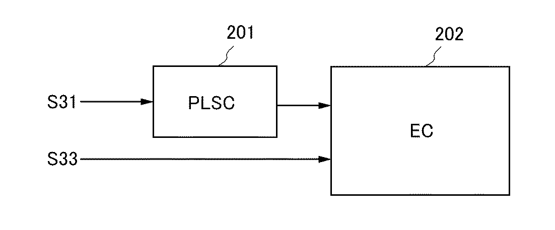
図10に示すように、電荷注入用のトランジスタと、リーク電流評価用のトランジスタと
を別々に設けることにより、電荷注入の際に、リーク電流評価用のトランジスタを常にオ
フ状態に保つことができる。電荷注入用のトランジスタを設けない場合には、電荷注入の
際に、リーク電流評価用トランジスタを一度オン状態にする必要があるが、オン状態から
オフ状態の定常状態に到るまでに時間を要するような素子では、測定に時間を要してしま
う。
As shown in FIG. 10, by separately providing a charge injection transistor and a leakage current evaluation transistor, the leakage current evaluation transistor can always be kept off during charge injection. When a charge injection transistor is not provided, it is necessary to turn on the leakage current evaluation transistor once at the time of charge injection, but it takes time to reach the steady state from the on state to the off state. In such an element, measurement takes time.
また、電荷注入用のトランジスタと、リーク電流評価用のトランジスタとを別々に設ける
ことにより、それぞれのトランジスタを適切なサイズとすることができる。また、リーク
電流評価用トランジスタのチャネル幅Wを、電荷注入用のトランジスタのチャネル幅Wよ
りも大きくすることにより、リーク電流評価用トランジスタのリーク電流以外の特性評価
回路のリーク電流成分を相対的に小さくすることができる。その結果、リーク電流評価用
トランジスタのリーク電流を高い精度で測定することができる。同時に、電荷注入の際に
、リーク電流評価用トランジスタを一度オン状態とする必要がないため、リーク電流評価
用トランジスタのチャネル形成領域の電荷の一部がノードAに流れ込むことによるノード
Aの電圧変動の影響もない。
Further, by separately providing a charge injection transistor and a leakage current evaluation transistor, each transistor can be appropriately sized. Further, by making the channel width W of the leakage current evaluation transistor larger than the channel width W of the charge injection transistor, the leakage current component of the characteristic evaluation circuit other than the leakage current of the leakage current evaluation transistor is relatively Can be small. As a result, the leakage current of the leakage current evaluation transistor can be measured with high accuracy. At the same time, since it is not necessary to turn on the leakage current evaluation transistor once at the time of charge injection, voltage fluctuation of node A due to a part of the charge in the channel formation region of the leakage current evaluation transistor flowing into node A There is no influence.
一方、電荷注入用トランジスタのチャネル幅Wを、リーク電流評価用トランジスタのチャ
ネル幅Wよりも小さくすることにより、電荷注入用トランジスタのリーク電流を相対的に
小さくすることができる。また、電荷注入の際に、電荷注入用トランジスタのチャネル形
成領域の電荷の一部がノードAに流れ込むことによるノードAの電圧変動の影響も小さい
。
On the other hand, by making the channel width W of the charge injection transistor smaller than the channel width W of the leakage current evaluation transistor, the leakage current of the charge injection transistor can be relatively reduced. In addition, the influence of voltage fluctuation at the node A due to a part of the charge in the channel formation region of the charge injection transistor flowing into the node A during charge injection is small.
また、図10に示すように、複数の測定系を並列接続させた構造にすることにより、より
正確に特性評価回路のリーク電流を算出することができる。
In addition, as shown in FIG. 10, the leakage current of the characteristic evaluation circuit can be calculated more accurately by adopting a structure in which a plurality of measurement systems are connected in parallel.
次に、図10に示す特性評価回路を用いた、本実施の形態のトランジスタの一例のオフ電
流の値の算出方法について説明する。
Next, a method for calculating the off-state current value of an example of the transistor of this embodiment using the characteristic evaluation circuit illustrated in FIG. 10 will be described.
まず、図10に示す特性評価回路のリーク電流測定方法について、図11を用いて説明す
る。図11は、図10に示す特性評価回路を用いたリーク電流測定方法を説明するための
タイミングチャートである。
First, a method for measuring leakage current of the characteristic evaluation circuit shown in FIG. 10 will be described with reference to FIG. FIG. 11 is a timing chart for explaining a leakage current measuring method using the characteristic evaluation circuit shown in FIG.
図10に示す特性評価回路を用いたリーク電流測定方法は、書き込み期間及び保持期間に
分けられる。それぞれの期間における動作について、以下に説明する。
The leakage current measuring method using the characteristic evaluation circuit shown in FIG. 10 is divided into a writing period and a holding period. The operation in each period will be described below.
まず、書き込み期間において、電圧Vext_bとして、トランジスタ812がオフ状態
となるような電圧VL(−3V)を入力する。また、電圧V1として、書き込み電圧Vw
を入力した後、電圧Vext_aとして、一定期間トランジスタ811がオン状態となる
ような電圧VH(5V)を入力する。これによって、ノードAに電荷が蓄積され、ノード
Aの電圧は、書き込み電圧Vwと同等の値になる。その後、電圧Vext_aとして、ト
ランジスタ811がオフ状態となるような電圧VLを入力する。その後、電圧V1として
、電圧VSS(0V)を入力する。
First, in the writing period, a voltage VL (−3 V) that turns off the
Is input as the voltage Vext_a, a voltage VH (5 V) that keeps the
その後、保持期間において、ノードAが保持する電荷量の変化に起因して生じるノードA
の電圧の変化量の測定を行う。電圧の変化量から、トランジスタ812のソース電極とド
レイン電極との間を流れる電流値を算出することができる。以上により、ノードAの電荷
の蓄積とノードAの電圧の変化量の測定とを行うことができる。
After that, in the holding period, the node A generated due to the change in the amount of charge held by the node A
Measure the amount of voltage change. From the amount of change in voltage, the value of the current flowing between the source electrode and the drain electrode of the
このとき、ノードAの電荷の蓄積及びノードAの電圧の変化量の測定(蓄積及び測定動作
ともいう)を繰り返し行う。まず、第1の蓄積及び測定動作を15回繰り返し行う。第1
の蓄積及び測定動作では、書き込み期間に書き込み電圧Vwとして5Vの電圧を入力し、
保持期間に1時間の保持を行う。次に、第2の蓄積及び測定動作を2回繰り返し行う。第
2の蓄積及び測定動作では、書き込み期間に書き込み電圧Vwとして3.5Vの電圧を入
力し、保持期間に50時間の保持を行う。次に、第3の蓄積及び測定動作を1回行う。第
3の蓄積及び測定動作では、書き込み期間に書き込み電圧Vwとして4.5Vの電圧を入
力し、保持期間に10時間の保持を行う。蓄積及び測定動作を繰り返し行うことにより、
測定した電流値が、定常状態における値であることを確認することができる。言い換える
と、ノードAを流れる電流IAのうち、過渡電流(測定開始後から時間経過とともに減少
していく電流成分)を除くことができる。その結果、より高い精度でリーク電流を測定す
ることができる。
At this time, accumulation of charge at the node A and measurement of the amount of change in the voltage at the node A (also referred to as accumulation and measurement operation) are repeatedly performed. First, the first accumulation and measurement operation is repeated 15 times. First
In the accumulation and measurement operation, a voltage of 5 V is input as the write voltage Vw during the write period,
Hold for 1 hour during the holding period. Next, the second accumulation and measurement operation is repeated twice. In the second accumulation and measurement operation, a voltage of 3.5 V is input as the writing voltage Vw in the writing period, and holding for 50 hours is performed in the holding period. Next, the third accumulation and measurement operation is performed once. In the third accumulation and measurement operation, a voltage of 4.5 V is input as the writing voltage Vw in the writing period, and holding is performed for 10 hours in the holding period. By repeating the accumulation and measurement operations,
It can be confirmed that the measured current value is a value in a steady state. In other words, among the current I A flowing through the node A, it is possible to remove the transient current (current component decreases with the passage after the measurement start time). As a result, the leak current can be measured with higher accuracy.
一般に、ノードAの電圧VAは、出力電圧Voutの関数として式(1)のように表され
る。
In general, the voltage V A at the node A is expressed as the equation (1) as a function of the output voltage Vout.
また、ノードAの電荷QAは、ノードAの電圧VA、ノードAに接続される容量CA、定
数(const)を用いて、式(2)のように表される。ここで、ノードAに接続される
容量CAは、容量素子813の容量と容量素子813以外の容量成分の和である。
In addition, the charge Q A of the node A is expressed as in Expression (2) using the voltage V A of the node A, the capacitance C A connected to the node A, and a constant (const). Here, the capacitance C A connected to the node A, is the sum of the capacity component other than capacitance and the
ノードAの電流IAは、ノードAに流れ込む電荷(またはノードAから流れ出る電荷)の
時間微分であるから、ノードAの電流IAは、式(3)のように表される。
Current I A of the node A, since the time derivative of charge flowing to the node A (or node A charge flowing from), the current I A of the node A is expressed by the equation (3).
なお、ここでは、一例として、Δtを約54000secとする。このように、ノードA
に接続される容量CAと、出力電圧Voutから、リーク電流であるノードAの電流IA
を求めることができるため、特性評価回路のリーク電流を求めることができる。
Here, as an example, Δt is about 54000 sec. Thus, node A
From the capacitor C A connected to the output voltage Vout and the output voltage Vout, the current A A of the node A which is a leakage current
Therefore, the leakage current of the characteristic evaluation circuit can be obtained.
次に、上記特性評価回路を用いた測定方法による出力電圧の測定結果及び該測定結果より
算出した特性評価回路のリーク電流の値を示す。
Next, the measurement result of the output voltage by the measurement method using the characteristic evaluation circuit and the value of the leakage current of the characteristic evaluation circuit calculated from the measurement result are shown.
図12に、一例として、条件4、条件5、及び条件6における上記測定(第1の蓄積及び
測定動作)に係る経過時間Timeと、出力電圧Voutとの関係を示す。図13に、上
記測定に係る経過時間Timeと、該測定によって算出された電流IAとの関係を示す。
測定開始後から出力電圧Voutが変動しており、定常状態に到るためには10時間以上
必要であることがわかる。
FIG. 12 shows, as an example, the relationship between the elapsed time Time related to the above measurement (first accumulation and measurement operation) in condition 4,
It can be seen that the output voltage Vout has fluctuated since the start of measurement, and it takes 10 hours or more to reach a steady state.
また、図14に、上記測定により得られた値から見積もられた条件1乃至条件6における
ノードAの電圧とリーク電流の関係を示す。図14では、例えば条件4において、ノード
Aの電圧が3.0Vの場合、リーク電流は28yA/μmである。リーク電流にはトラン
ジスタ812のオフ電流も含まれるため、トランジスタ812のオフ電流も28yA/μ
m以下とみなすことができる。
FIG. 14 shows the relationship between the voltage of the node A and the leakage current under
m or less.
また、図15乃至図17に、85℃、125℃、及び150℃における上記測定により見
積もられた条件1乃至条件6におけるノードAの電圧とリーク電流の関係を示す。図15
乃至図17に示すように、150℃の場合であっても、リーク電流は、100zA/μm
以下であることがわかる。
15 to 17 show the relationship between the voltage of the node A and the leakage current under
As shown in FIG. 17, even at 150 ° C., the leakage current is 100 zA / μm.
It turns out that it is the following.
以上のように、チャネル形成層としての機能を有し、高純度化された酸化物半導体層を含
むトランジスタを用いた特性評価用回路において、リーク電流が十分に低いため、上記ト
ランジスタのオフ電流が十分に小さいことがわかる。また、上記トランジスタのオフ電流
は、温度が上昇した場合であっても十分に低いことがわかる。
As described above, in a circuit for evaluating characteristics using a transistor that functions as a channel formation layer and includes a highly purified oxide semiconductor layer, the leakage current is sufficiently low; It turns out that it is small enough. It can also be seen that the off-state current of the transistor is sufficiently low even when the temperature rises.
(実施の形態6)
本実施の形態では、上記実施の形態の記憶回路の構造例について説明する。
(Embodiment 6)
In this embodiment, structural examples of the memory circuit in the above embodiment will be described.
本実施の形態における記憶回路の構造例について、図18及び図19を用いて説明する。
図18及び図19は、本実施の形態における記憶回路の構造例を示す図であり、図18(
A)は、パルス変換回路の平面模式図であり、図18(B)は、図18(A)における線
分A−Bの断面模式図であり、図19(A)は、単位記憶回路の平面模式図であり、図1
9(B)は、図19(A)における線分C−Dの断面模式図であり、図19(C)は、図
19(A)における線分E−Fの断面模式図である。なお、図18及び図19では、酸化
物半導体層を含むトランジスタの一例として、上記実施の形態における、図7(A)を用
いて説明した構造のトランジスタを用いる場合を示す。
An example of a structure of the memory circuit in this embodiment will be described with reference to FIGS.
18 and 19 illustrate structural examples of the memory circuit in this embodiment.
FIG. 18A is a schematic plan view of a pulse conversion circuit, FIG. 18B is a schematic cross-sectional view taken along line AB in FIG. 18A, and FIG. FIG. 1 is a schematic plan view of FIG.
9B is a schematic cross-sectional view taken along line CD in FIG. 19A, and FIG. 19C is a schematic cross-sectional view taken along line EF in FIG. 19A. Note that FIGS. 18 and 19 illustrate the case where the transistor having the structure described with reference to FIG. 7A in the above embodiment is used as an example of a transistor including an oxide semiconductor layer.
図18及び図19に示す記憶回路は、半導体層502a乃至半導体層502cと、絶縁層
505と、導電層506aと、導電層506bと、絶縁層507と、導電層508a乃至
導電層508cと、絶縁層509と、半導体層510aと、半導体層510bと、導電層
511a乃至導電層511hと、絶縁層512と、導電層513a乃至導電層513cと
、を含む。
18 and 19 includes a
半導体層502a乃至半導体層502cのそれぞれは、絶縁層501を介して基板500
の一平面に設けられる。
Each of the
Provided on one plane.
半導体層502aは、互いに離間して設けられた不純物領域503a及び不純物領域50
4aを含む。半導体層502aは、パルス変換回路におけるP型トランジスタのチャネル
形成層としての機能を有する。また、不純物領域503aは、パルス変換回路におけるP
型トランジスタのソース領域及びドレイン領域の一方としての機能を有する。また、不純
物領域504aは、パルス変換回路におけるP型トランジスタのソース領域及びドレイン
領域の他方としての機能を有する。
The
4a is included. The
It functions as one of a source region and a drain region of a type transistor. In addition, the
半導体層502bは、単位記憶回路における保持容量の第1の電極としての機能を有する
。
The
半導体層502cは、互いに離間して設けられた不純物領域503b及び不純物領域50
4bを有する。半導体層502cは、単位記憶回路における出力用トランジスタのチャネ
ル形成層としての機能を有する。また、不純物領域503bは、単位記憶回路における出
力用トランジスタのソース領域及びドレイン領域の一方としての機能を有する。また、不
純物領域504bは、単位記憶回路における出力用トランジスタのソース領域及びドレイ
ン領域の他方としての機能を有する。
The
4b. The
絶縁層505は、半導体層502a乃至半導体層502c及び絶縁層501を介して基板
500の一平面に設けられる。絶縁層505は、パルス変換回路におけるP型トランジス
タのゲート絶縁層、単位記憶回路における保持容量の誘電体層、及び単位記憶回路におけ
る出力用トランジスタのゲート絶縁層としての機能を有する。
The insulating
導電層506aは、絶縁層505を介して半導体層502aに重畳する。導電層506a
は、パルス変換回路におけるP型トランジスタのゲート電極としての機能を有する。
The
Has a function as a gate electrode of a P-type transistor in the pulse conversion circuit.
導電層506bは、絶縁層505を介して半導体層502cに重畳する。導電層506b
は、単位記憶回路における出力用トランジスタのゲート電極としての機能を有する。
The
Has a function as a gate electrode of the output transistor in the unit memory circuit.
絶縁層507は、絶縁層505、導電層506a、及び導電層506bに積層される。絶
縁層507は、平坦化絶縁層としての機能を有する。
The insulating
導電層508a及び導電層508bは、絶縁層507に積層される。
The
導電層508aは、パルス変換回路におけるN型トランジスタのゲート電極としての機能
を有する。
The
導電層508bは、単位記憶回路における選択用トランジスタのゲート電極としての機能
を有する。
The
導電層508cは、絶縁層505及び絶縁層507を介して半導体層502bに重畳する
。また、導電層508cは、単位記憶回路における保持容量の第2の電極としての機能を
有する。
The
絶縁層509は、絶縁層507及び導電層508a乃至導電層508cに積層される。絶
縁層509は、パルス変換回路におけるN型トランジスタのゲート絶縁層及び単位記憶回
路における選択用トランジスタのゲート絶縁層としての機能を有する。
The insulating
半導体層510aは、絶縁層509を介して導電層508aに重畳する。半導体層510
aは、パルス変換回路におけるN型トランジスタのチャネル形成層としての機能を有する
。
The
a has a function as a channel formation layer of the N-type transistor in the pulse conversion circuit.
半導体層510bは、絶縁層509を介して導電層508bに重畳する。半導体層510
bは、単位記憶回路における選択用トランジスタのチャネル形成層としての機能を有する
。
The
b has a function as a channel formation layer of the selection transistor in the unit memory circuit.
導電層511aは、半導体層502aにおける不純物領域503aに電気的に接続される
。導電層511aは、パルス変換回路におけるP型トランジスタのソース電極及びドレイ
ン電極の一方としての機能を有する。
The
導電層511bは、半導体層502bにおける不純物領域504a及び半導体層510a
に電気的に接続される。導電層511bは、パルス変換回路におけるP型トランジスタの
ソース電極及びドレイン電極の他方、並びにパルス変換回路におけるN型トランジスタの
ソース電極及びドレイン電極の一方としての機能を有する。
The
Is electrically connected. The
導電層511cは、半導体層510aに電気的に接続される。導電層511cは、パルス
変換回路におけるN型トランジスタのソース電極及びドレイン電極の他方としての機能を
有する。
The
導電層511dは、半導体層510bに電気的に接続される。導電層511dは、単位記
憶回路における選択用トランジスタのソース電極及びドレイン電極の一方としての機能を
有する。
The
導電層511eは、半導体層510bに電気的に接続される。導電層511eは、単位記
憶回路における選択用トランジスタのソース電極及びドレイン電極の他方としての機能を
有する。
The
導電層511fは、半導体層502cにおける不純物領域503bに電気的に接続される
。導電層511fは、単位記憶回路における出力用トランジスタのソース電極及びドレイ
ン電極の一方としての機能を有する。
The
導電層511gは、半導体層502cにおける不純物領域504bに電気的に接続される
。導電層511gは、単位記憶回路における出力用トランジスタのソース電極及びドレイ
ン電極の他方としての機能を有する。
The
導電層511hは、絶縁層509に積層される。また、導電層511hは、単位記憶回路
においてデータ信号が入力されるビット線としての機能を有する。
The
絶縁層512は、絶縁層509、半導体層510a、半導体層510b、及び導電層51
1a乃至導電層511hに接する。
The insulating
1a thru | or the
導電層513aは、導電層508bに電気的に接続される。導電層513aは、単位記憶
回路において行アドレス信号が入力されるワード線としての機能を有する。なお、導電層
513aを必ずしも設けなくてもよく、導電層508bがワード線としての機能を有する
構成にしてもよい。
The
導電層513bは、導電層508cに電気的に接続される。導電層513bは、単位記憶
回路において読み出し信号が入力される読み出し線としての機能を有する。なお、導電層
513bを必ずしも設けなくてもよく、導電層508cが読み出し線としての機能を有す
る構成にしてもよい。
The
導電層513cは、導電層511d及び導電層511hに電気的に接続される。
The
基板500としては、図7(A)における基板400aに適用可能な基板を用いることが
できる。
As the
絶縁層501としては、図7(D)における絶縁層447に適用可能な材料の層を用いる
ことができる。また、絶縁層501に適用可能な材料の層を積層して絶縁層501を構成
してもよい。
As the insulating
半導体層502a乃至半導体層502cとしては、元素周期表における第14族の半導体
(シリコンなど)を含有する半導体層を用いることができる。
As the
不純物領域503a及び不純物領域504aは、P型の導電性を付与する不純物元素を添
加することにより形成される。また、不純物領域503b及び不純物領域504bは、P
型又はN型の導電性を付与する不純物元素を添加することにより形成される。P型の導電
性を付与する不純物元素としては、例えばボロンなどを用いることができ、N型の導電性
を付与する不純物元素としては、例えばリンなどを用いることができる。
The
It is formed by adding an impurity element imparting type or N type conductivity. For example, boron or the like can be used as the impurity element imparting P-type conductivity, and phosphorus or the like can be used as the impurity element imparting N-type conductivity, for example.
絶縁層505及び絶縁層509としては、図7(A)における絶縁層402aに適用可能
な材料の層を用いることができる。また、絶縁層505及び絶縁層509に適用可能な材
料の層を積層して絶縁層505及び絶縁層509を構成してもよい。
As the insulating
導電層506a、導電層506b、及び導電層508a乃至導電層508cとしては、例
えば図7(A)における導電層401aに適用可能な材料の層を用いることができる。ま
た、導電層506a、導電層506b、及び導電層508a乃至導電層508cに適用可
能な材料の層を積層して導電層506a、導電層506b、及び導電層508a乃至導電
層508cを構成してもよい。
As the
絶縁層507としては、例えばポリイミド、アクリル、ベンゾシクロブテン、などの有機
材料の層を用いることができる。また平坦化絶縁層としては、低誘電率材料(low−k
材料ともいう)の層を用いることもできる。また、絶縁層507に適用可能な材料の層の
積層により絶縁層507を構成することもできる。
As the insulating
(Also referred to as a material) can be used. Alternatively, the insulating
半導体層510a及び半導体層510bとしては、図7(A)に示す酸化物半導体層40
3aに適用可能な材料の層を用いることができる。
As the
A layer of material applicable to 3a can be used.
導電層511a乃至導電層511h、及び導電層513a乃至導電層513cとしては、
図7(A)における導電層405a又は導電層406aに適用可能な材料の層を用いるこ
とができる。また、導電層511a乃至導電層511h及び導電層513a乃至導電層5
13cに適用可能な材料の層を積層して導電層511a乃至導電層511h及び導電層5
13a乃至導電層513cを構成してもよい。
As the
A layer of a material that can be used for the
A layer of a material applicable to 13c is stacked to form
The conductive layers 13a to 513c may be configured.
絶縁層512としては、図7(A)における酸化物絶縁層407aに適用可能な材料の層
を用いることができる。また、絶縁層512に適用可能な層を積層して絶縁層512を構
成してもよい。
As the insulating
図18及び図19を用いて説明したように、本実施の形態の記憶回路は、同一基板上にパ
ルス変換回路及び単位記憶回路を備える構造である。上記構造にすることにより同一工程
でパルス変換回路及び単位記憶回路を作製することができるため、製造コストを低減する
ことができる。なお、本実施の形態の記憶回路を、パルス変換回路及び単位記憶回路と、
他の回路(第1の駆動回路、第2の駆動回路、及び制御回路の一つ又は複数)と、を同一
基板上に備える構造としてもよい。
As described with reference to FIGS. 18 and 19, the memory circuit of this embodiment has a structure including a pulse conversion circuit and a unit memory circuit over the same substrate. With the above structure, a pulse conversion circuit and a unit memory circuit can be manufactured in the same process, so that manufacturing costs can be reduced. Note that the memory circuit of this embodiment includes a pulse converter circuit and a unit memory circuit,
Another circuit (one or more of the first drive circuit, the second drive circuit, and the control circuit) may be provided on the same substrate.
(実施の形態7)
本実施の形態では、上記実施の形態の無線通信により信号の送受信が可能な半導体装置を
備えた情報媒体について説明する。
(Embodiment 7)
In this embodiment, an information medium including a semiconductor device capable of transmitting and receiving signals by wireless communication of the above embodiment will be described.
本実施の形態における情報媒体の構成例について、図20を用いて説明する。図20は、
本実施の形態における情報媒体の構成例を示す図である。
A configuration example of the information medium in this embodiment will be described with reference to FIG. FIG.
It is a figure which shows the structural example of the information medium in this Embodiment.
図20(A)に示す情報媒体は、個人情報が記載されたカード型証明書である。図20(
A)に示すカード型証明書は、チップ900を有する。図20(A)に示すカード型証明
書は、チップ900を設けることにより、偽造防止など、セキュリティ機能を向上させる
ことができる。カード型証明書としては、例えば、免許証又は住民票などが挙げられる。
チップ900は、信頼性が高いため、上記カード型証明書などの長い期間使用するものに
好適である。
The information medium shown in FIG. 20A is a card type certificate in which personal information is described. FIG.
The card type certificate shown in A) has a
Since the
図20(B)に示す情報媒体は、チケット型情報媒体である。図20(B)に示すチケッ
ト型情報媒体は、チップ901を有する。図20(B)に示すチケット型情報媒体は、チ
ップ901を設けることにより、チケット型情報媒体に記載された情報以外の情報をチッ
プ901に記録しておくことができる。また、図20(B)に示すチケット型情報媒体は
、チップ901を設けることにより、偽造防止など、セキュリティ機能を向上させること
ができる。なお、チップ901は、信頼性が高いため、例えばチケットの一部に切り取り
部を設け、チケット型情報媒体が不要になった際に、該切り取り部によりチップ901の
みを切り取って回収し、チップ901のみを再利用することもできる。チケット型情報媒
体としては、例えば紙幣又は乗車券、有価証券、若しくはその他の券などが挙げられる。
The information medium shown in FIG. 20B is a ticket type information medium. A ticket-type information medium illustrated in FIG. 20B includes a
図20(C)に示す情報媒体は、コイン型情報媒体である。コイン型情報媒体は、チップ
902を有する。図20(C)に示すコイン型情報媒体は、チップ902を設けることに
より、コイン型情報媒体に記載された情報以外の情報をチップ902に記録しておくこと
ができる。また、図20(C)に示すコイン型情報媒体は、チップ902を設けることに
より、偽造防止など、セキュリティ機能を向上させることができる。コイン型情報媒体と
しては、例えば硬貨又は乗車券、有価証券、若しくはその他の券などが挙げられる。
The information medium illustrated in FIG. 20C is a coin-type information medium. The coin-type information medium has a
図20(D)に示す情報媒体は、物品である。物品は、チップ903を有する。図20(
D)に示す物品は、チップ903を設けることにより、物品に記載された情報以外の情報
をチップ903に記録しておくことができる。また、図20(D)に示す物品は、チップ
903を設けることにより、偽造防止など、セキュリティ機能を向上させることができる
。なお、物品としては、特に限定されず、例えば電化製品又は生活用品など様々なものが
挙げられる。
The information medium illustrated in FIG. 20D is an article. The article has a
The article shown in D) can record information other than the information described in the article on the
チップ900乃至チップ903としては、例えば上記実施の形態に示す無線通信が可能な
半導体装置を適用することができる。
As the
図20を用いて説明したように、本実施の形態の情報媒体の一例は、無線通信可能なチッ
プを有する構成である。上記構成にすることにより、回路面積を小さくすることができる
。また、上記構成にすることにより、無線通信によりチップが設けられた情報媒体の固有
情報を読み出し、読み出した固有情報を利用することができる。これにより、情報媒体の
管理が容易になり、また、セキュリティ性を向上させることができる。
As described with reference to FIG. 20, an example of the information medium of this embodiment has a structure having a chip capable of wireless communication. With the above configuration, the circuit area can be reduced. Further, with the above configuration, the unique information of the information medium provided with the chip can be read by wireless communication, and the read unique information can be used. As a result, management of the information medium is facilitated, and security can be improved.
101 トランジスタ
102 トランジスタ
151 インバータ
152 インバータ
201 パルス変換回路
202 機能回路
211 単位記憶回路
213v 駆動制御回路
213w パルス変換回路
213x 第1の駆動回路
213y 第2の駆動回路
231 トランジスタ
232 容量素子
233 トランジスタ
301 アンテナ回路
302 電源回路
303 復調回路
304 記憶制御回路
305 記憶回路
306 符号化回路
307 変調回路
400a 基板
400b 基板
400c 基板
400d 基板
401a 導電層
401b 導電層
401c 導電層
401d 導電層
402a 絶縁層
402b 絶縁層
402c 絶縁層
402d 絶縁層
403a 酸化物半導体層
403b 酸化物半導体層
403c 酸化物半導体層
403d 酸化物半導体層
405a 導電層
405b 導電層
405c 導電層
405d 導電層
406a 導電層
406b 導電層
406c 導電層
406d 導電層
407a 酸化物絶縁層
407c 酸化物絶縁層
427 絶縁層
447 絶縁層
500 基板
501 絶縁層
502a 半導体層
502b 半導体層
502c 半導体層
503a 不純物領域
503b 不純物領域
504a 不純物領域
504b 不純物領域
505 絶縁層
506a 導電層
506b 導電層
507 絶縁層
508a 導電層
508b 導電層
508c 導電層
509 絶縁層
510a 半導体層
510b 半導体層
511a 導電層
511b 導電層
511c 導電層
511d 導電層
511e 導電層
511f 導電層
511g 導電層
511h 導電層
512 絶縁層
513a 導電層
513b 導電層
513c 導電層
801 測定系
811 トランジスタ
812 トランジスタ
813 容量素子
814 トランジスタ
815 トランジスタ
900 チップ
901 チップ
902 チップ
903 チップ
101 transistor 102 transistor 151 inverter 152 inverter 201 pulse conversion circuit 202 function circuit 211 unit storage circuit 213v drive control circuit 213w pulse conversion circuit 213x first drive circuit 213y second drive circuit 231 transistor 232 capacitor 233 transistor 301 antenna circuit 302 Power supply circuit 303 Demodulation circuit 304 Storage control circuit 305 Storage circuit 306 Encoding circuit 307 Modulation circuit 400a Substrate 400b Substrate 400c Substrate 400d Substrate 401a Conductive layer 401b Conductive layer 401c Conductive layer 401d Conductive layer 402a Insulating layer 402b Insulating layer 402c Insulating layer 402d Insulating Layer 403a oxide semiconductor layer 403b oxide semiconductor layer 403c oxide semiconductor layer 403d oxide semiconductor layer 405a conductive layer 405b conductive layer 05c conductive layer 405d conductive layer 406a conductive layer 406b conductive layer 406c conductive layer 406d conductive layer 407a oxide insulating layer 407c oxide insulating layer 427 insulating layer 447 insulating layer 500 substrate 501 insulating layer 502a semiconductor layer 502b semiconductor layer 502c semiconductor layer 503a impurity Region 503b Impurity region 504a Impurity region 504b Impurity region 505 Insulating layer 506a Conductive layer 506b Conductive layer 507 Insulating layer 508a Conductive layer 508b Conductive layer 508c Conductive layer 509 Insulating layer 510a Semiconductor layer 510b Semiconductor layer 511a Conductive layer 511b Conductive layer 511c Conductive layer 511d Conductive layer 511e Conductive layer 511f Conductive layer 511g Conductive layer 511h Conductive layer 512 Insulating layer 513a Conductive layer 513b Conductive layer 513c Conductive layer 801 Measurement system 811 Transistor 812 Transition Star 813 capacitor 814 transistor 815 transistor 900 chip 901 chip 902 chip 903 chip
Claims (2)
前記第1乃至第3の半導体層上の第1の絶縁層と、
前記第1の絶縁層上の、前記第1の半導体層と重なる第1の導電層と、
前記第1の絶縁層上の、前記第3の半導体層と重なる第2の導電層と、
前記第1の絶縁層、前記第1の導電層、及び前記第2の導電層上の第2の絶縁層と、
前記第2の絶縁層上の第3の導電層と、
前記第2の絶縁層上の第4の導電層と、
前記第2の絶縁層上の、前記第2の半導体層と重なる第5の導電層と、
前記第2の絶縁層、前記第3の導電層、前記第4の導電層、及び前記第5の導電層上の第3の絶縁層と、
前記第3の絶縁層上の、前記第3の導電層と重なる第4の半導体層と、
前記第3の絶縁層上の、前記第4の導電層と重なる第5の半導体層と、
前記第3の絶縁層上の、前記第1の半導体層と電気的に接続された第6の導電層と、
前記第3の絶縁層上の、前記第1の半導体層及び前記第4の半導体層と電気的に接続された第7の導電層と、
前記第3の絶縁層上の、前記第4の半導体層と電気的に接続された第8の導電層と、
前記第3の絶縁層上の、前記第5の半導体層と電気的に接続された第9の導電層と、
前記第3の絶縁層上の、前記第2の半導体層及び前記第5の半導体層と電気的に接続された第10の導電層と、
前記第3の絶縁層上の、前記第3の半導体層と電気的に接続された第11の導電層と、
前記第3の絶縁層上の、前記第3の半導体層と電気的に接続された第12の導電層と、を有し、
前記第1の半導体層は、パルス変換回路におけるP型トランジスタのチャネル形成層としての機能を有し、
前記第2の半導体層は、単位記憶回路における保持容量の第1の電極としての機能を有し、
前記第3の半導体層は、前記単位記憶回路における出力用トランジスタのチャネル形成層としての機能を有し、
前記第4の半導体層は、前記パルス変換回路におけるN型トランジスタのチャネル形成層としての機能を有し、
前記第5の半導体層は、前記単位記憶回路における選択用トランジスタのチャネル形成層としての機能を有することを特徴とする半導体装置。 First to third semiconductor layers on a substrate;
A first insulating layer on the first to third semiconductor layers;
A first conductive layer overlying the first semiconductor layer on the first insulating layer;
A second conductive layer overlying the third semiconductor layer on the first insulating layer;
A second insulating layer on the first insulating layer, the first conductive layer, and the second conductive layer;
A third conductive layer on the second insulating layer;
A fourth conductive layer on the second insulating layer;
A fifth conductive layer overlying the second semiconductor layer on the second insulating layer;
A third insulating layer on the second insulating layer, the third conductive layer, the fourth conductive layer, and the fifth conductive layer;
A fourth semiconductor layer overlying the third conductive layer on the third insulating layer;
A fifth semiconductor layer overlying the fourth conductive layer on the third insulating layer;
A sixth conductive layer electrically connected to the first semiconductor layer on the third insulating layer;
A seventh conductive layer electrically connected to the first semiconductor layer and the fourth semiconductor layer on the third insulating layer;
An eighth conductive layer electrically connected to the fourth semiconductor layer on the third insulating layer;
A ninth conductive layer electrically connected to the fifth semiconductor layer on the third insulating layer;
A tenth conductive layer electrically connected to the second semiconductor layer and the fifth semiconductor layer on the third insulating layer;
An eleventh conductive layer electrically connected to the third semiconductor layer on the third insulating layer;
A twelfth conductive layer electrically connected to the third semiconductor layer on the third insulating layer;
The first semiconductor layer has a function as a channel formation layer of a P-type transistor in the pulse conversion circuit,
The second semiconductor layer has a function as a first electrode of a storage capacitor in the unit memory circuit,
The third semiconductor layer has a function as a channel formation layer of an output transistor in the unit memory circuit,
The fourth semiconductor layer has a function as a channel formation layer of an N-type transistor in the pulse conversion circuit,
The fifth semiconductor layer has a function as a channel formation layer of a selection transistor in the unit memory circuit.
前記第4の半導体層及び前記第5の半導体層は、酸化物半導体を有することを特徴とする半導体装置。 In claim 1,
The fourth semiconductor layer and the fifth semiconductor layer each include an oxide semiconductor.
Applications Claiming Priority (2)
| Application Number | Priority Date | Filing Date | Title |
|---|---|---|---|
| JP2010116861 | 2010-05-21 | ||
| JP2010116861 | 2010-05-21 |
Related Parent Applications (1)
| Application Number | Title | Priority Date | Filing Date |
|---|---|---|---|
| JP2015049476A Division JP2015146606A (en) | 2010-05-21 | 2015-03-12 | semiconductor device |
Publications (2)
| Publication Number | Publication Date |
|---|---|
| JP2017022397A JP2017022397A (en) | 2017-01-26 |
| JP6173548B2 true JP6173548B2 (en) | 2017-08-02 |
Family
ID=44972009
Family Applications (3)
| Application Number | Title | Priority Date | Filing Date |
|---|---|---|---|
| JP2011105042A Expired - Fee Related JP5714973B2 (en) | 2010-05-21 | 2011-05-10 | Semiconductor device |
| JP2015049476A Withdrawn JP2015146606A (en) | 2010-05-21 | 2015-03-12 | semiconductor device |
| JP2016174210A Expired - Fee Related JP6173548B2 (en) | 2010-05-21 | 2016-09-07 | Semiconductor device |
Family Applications Before (2)
| Application Number | Title | Priority Date | Filing Date |
|---|---|---|---|
| JP2011105042A Expired - Fee Related JP5714973B2 (en) | 2010-05-21 | 2011-05-10 | Semiconductor device |
| JP2015049476A Withdrawn JP2015146606A (en) | 2010-05-21 | 2015-03-12 | semiconductor device |
Country Status (3)
| Country | Link |
|---|---|
| US (2) | US9209206B2 (en) |
| JP (3) | JP5714973B2 (en) |
| CN (1) | CN102355252B (en) |
Cited By (2)
| Publication number | Priority date | Publication date | Assignee | Title |
|---|---|---|---|---|
| US9850702B2 (en) | 2003-08-20 | 2017-12-26 | Hunter Douglas Inc | Method for making a window covering having operable vanes |
| US10030438B2 (en) | 2003-08-20 | 2018-07-24 | Hunter Douglas Inc. | Retractable shade with collapsible vanes |
Families Citing this family (15)
| Publication number | Priority date | Publication date | Assignee | Title |
|---|---|---|---|---|
| KR101874144B1 (en) | 2011-05-06 | 2018-07-03 | 가부시키가이샤 한도오따이 에네루기 켄큐쇼 | Semiconductor memory device |
| TWI568181B (en) | 2011-05-06 | 2017-01-21 | 半導體能源研究所股份有限公司 | Logic circuit and semiconductor device |
| TWI536502B (en) | 2011-05-13 | 2016-06-01 | 半導體能源研究所股份有限公司 | Memory circuit and electronic device |
| JP5947099B2 (en) | 2011-05-20 | 2016-07-06 | 株式会社半導体エネルギー研究所 | Semiconductor device |
| JP5951351B2 (en) | 2011-05-20 | 2016-07-13 | 株式会社半導体エネルギー研究所 | Adder and full adder |
| US8508256B2 (en) | 2011-05-20 | 2013-08-13 | Semiconductor Energy Laboratory Co., Ltd. | Semiconductor integrated circuit |
| JP2013016243A (en) * | 2011-06-09 | 2013-01-24 | Semiconductor Energy Lab Co Ltd | Memory device |
| US8736315B2 (en) | 2011-09-30 | 2014-05-27 | Semiconductor Energy Laboratory Co., Ltd. | Semiconductor device |
| JP6099372B2 (en) | 2011-12-05 | 2017-03-22 | 株式会社半導体エネルギー研究所 | Semiconductor device and electronic equipment |
| JP2013232548A (en) * | 2012-04-27 | 2013-11-14 | Panasonic Corp | Thin film transistor device manufacturing method, thin film transistor device and display device |
| US9135182B2 (en) | 2012-06-01 | 2015-09-15 | Semiconductor Energy Laboratory Co., Ltd. | Central processing unit and driving method thereof |
| US9515661B2 (en) * | 2014-05-09 | 2016-12-06 | Semiconductor Energy Laboratory Co., Ltd. | Circuit, semiconductor device, and clock tree |
| US10056497B2 (en) | 2015-04-15 | 2018-08-21 | Semiconductor Energy Laboratory Co., Ltd. | Semiconductor device and manufacturing method thereof |
| US10559696B2 (en) * | 2017-10-11 | 2020-02-11 | Shenzhen China Star Optoelectronics Semiconductor Display Technology Co., Ltd. | Hybrid CMOS device and manufacturing method thereof |
| JP6448743B2 (en) * | 2017-10-30 | 2019-01-09 | 株式会社半導体エネルギー研究所 | Semiconductor device |
Family Cites Families (125)
| Publication number | Priority date | Publication date | Assignee | Title |
|---|---|---|---|---|
| JPS60198861A (en) | 1984-03-23 | 1985-10-08 | Fujitsu Ltd | Thin film transistor |
| JPH0244256B2 (en) | 1987-01-28 | 1990-10-03 | Kagaku Gijutsucho Mukizaishitsu Kenkyushocho | INGAZN2O5DESHIMESARERUROTSUHOSHOKEINOSOJOKOZOOJUSURUKAGOBUTSUOYOBISONOSEIZOHO |
| JPH0244260B2 (en) | 1987-02-24 | 1990-10-03 | Kagaku Gijutsucho Mukizaishitsu Kenkyushocho | INGAZN5O8DESHIMESARERUROTSUHOSHOKEINOSOJOKOZOOJUSURUKAGOBUTSUOYOBISONOSEIZOHO |
| JPH0244258B2 (en) | 1987-02-24 | 1990-10-03 | Kagaku Gijutsucho Mukizaishitsu Kenkyushocho | INGAZN3O6DESHIMESARERUROTSUHOSHOKEINOSOJOKOZOOJUSURUKAGOBUTSUOYOBISONOSEIZOHO |
| JPS63210023A (en) | 1987-02-24 | 1988-08-31 | Natl Inst For Res In Inorg Mater | Compound having laminar structure of hexagonal crystal system expressed by ingazn4o7 and its production |
| JPH0244262B2 (en) | 1987-02-27 | 1990-10-03 | Kagaku Gijutsucho Mukizaishitsu Kenkyushocho | INGAZN6O9DESHIMESARERUROTSUHOSHOKEINOSOJOKOZOOJUSURUKAGOBUTSUOYOBISONOSEIZOHO |
| JPH0244263B2 (en) | 1987-04-22 | 1990-10-03 | Kagaku Gijutsucho Mukizaishitsu Kenkyushocho | INGAZN7O10DESHIMESARERUROTSUHOSHOKEINOSOJOKOZOOJUSURUKAGOBUTSUOYOBISONOSEIZOHO |
| JPH05251705A (en) | 1992-03-04 | 1993-09-28 | Fuji Xerox Co Ltd | Thin-film transistor |
| JP2655053B2 (en) | 1993-11-01 | 1997-09-17 | 日本電気株式会社 | Semiconductor integrated circuit device |
| EP0653843A3 (en) | 1993-11-17 | 1996-05-01 | Hewlett Packard Co | Adaptive threshold voltage CMOS circuits. |
| JPH07202677A (en) | 1993-12-27 | 1995-08-04 | Nippon Telegr & Teleph Corp <Ntt> | Cmos output buffer circuit |
| JP3479375B2 (en) | 1995-03-27 | 2003-12-15 | 科学技術振興事業団 | Metal oxide semiconductor device in which a pn junction is formed with a thin film transistor made of a metal oxide semiconductor such as cuprous oxide, and methods for manufacturing the same |
| DE69635107D1 (en) | 1995-08-03 | 2005-09-29 | Koninkl Philips Electronics Nv | SEMICONDUCTOR ARRANGEMENT WITH A TRANSPARENT CIRCUIT ELEMENT |
| JP3625598B2 (en) | 1995-12-30 | 2005-03-02 | 三星電子株式会社 | Manufacturing method of liquid crystal display device |
| JP3333429B2 (en) | 1997-06-30 | 2002-10-15 | 株式会社東芝 | Semiconductor integrated circuit |
| JPH11233789A (en) | 1998-02-12 | 1999-08-27 | Semiconductor Energy Lab Co Ltd | Semiconductor device |
| JP4170454B2 (en) | 1998-07-24 | 2008-10-22 | Hoya株式会社 | Article having transparent conductive oxide thin film and method for producing the same |
| JP2000150861A (en) | 1998-11-16 | 2000-05-30 | Tdk Corp | Oxide thin film |
| JP3276930B2 (en) | 1998-11-17 | 2002-04-22 | 科学技術振興事業団 | Transistor and semiconductor device |
| JP2001053164A (en) | 1999-08-04 | 2001-02-23 | Sony Corp | Semiconductor storage device |
| TW460731B (en) | 1999-09-03 | 2001-10-21 | Ind Tech Res Inst | Electrode structure and production method of wide viewing angle LCD |
| JP4089858B2 (en) | 2000-09-01 | 2008-05-28 | 国立大学法人東北大学 | Semiconductor device |
| KR20020038482A (en) | 2000-11-15 | 2002-05-23 | 모리시타 요이찌 | Thin film transistor array, method for producing the same, and display panel using the same |
| JP3997731B2 (en) | 2001-03-19 | 2007-10-24 | 富士ゼロックス株式会社 | Method for forming a crystalline semiconductor thin film on a substrate |
| JP2002289859A (en) | 2001-03-23 | 2002-10-04 | Minolta Co Ltd | Thin-film transistor |
| JP4090716B2 (en) | 2001-09-10 | 2008-05-28 | 雅司 川崎 | Thin film transistor and matrix display device |
| JP3925839B2 (en) | 2001-09-10 | 2007-06-06 | シャープ株式会社 | Semiconductor memory device and test method thereof |
| US7061014B2 (en) | 2001-11-05 | 2006-06-13 | Japan Science And Technology Agency | Natural-superlattice homologous single crystal thin film, method for preparation thereof, and device using said single crystal thin film |
| JP4164562B2 (en) | 2002-09-11 | 2008-10-15 | 独立行政法人科学技術振興機構 | Transparent thin film field effect transistor using homologous thin film as active layer |
| JP2003188266A (en) | 2001-12-19 | 2003-07-04 | Sony Corp | Delay circuit |
| JP4083486B2 (en) | 2002-02-21 | 2008-04-30 | 独立行政法人科学技術振興機構 | Method for producing LnCuO (S, Se, Te) single crystal thin film |
| CN1445821A (en) | 2002-03-15 | 2003-10-01 | 三洋电机株式会社 | Forming method of ZnO film and ZnO semiconductor layer, semiconductor element and manufacturing method thereof |
| JP3933591B2 (en) | 2002-03-26 | 2007-06-20 | 淳二 城戸 | Organic electroluminescent device |
| US7339187B2 (en) | 2002-05-21 | 2008-03-04 | State Of Oregon Acting By And Through The Oregon State Board Of Higher Education On Behalf Of Oregon State University | Transistor structures |
| JP2004022625A (en) | 2002-06-13 | 2004-01-22 | Murata Mfg Co Ltd | Manufacturing method of semiconductor device and its manufacturing method |
| US7105868B2 (en) | 2002-06-24 | 2006-09-12 | Cermet, Inc. | High-electron mobility transistor with zinc oxide |
| US7067843B2 (en) | 2002-10-11 | 2006-06-27 | E. I. Du Pont De Nemours And Company | Transparent oxide semiconductor thin film transistors |
| JP2004200426A (en) * | 2002-12-19 | 2004-07-15 | Nec Electronics Corp | Semiconductor integrated circuit device |
| JP4166105B2 (en) | 2003-03-06 | 2008-10-15 | シャープ株式会社 | Semiconductor device and manufacturing method thereof |
| JP2004273732A (en) | 2003-03-07 | 2004-09-30 | Sharp Corp | Active matrix substrate and its producing process |
| JP4108633B2 (en) | 2003-06-20 | 2008-06-25 | シャープ株式会社 | THIN FILM TRANSISTOR, MANUFACTURING METHOD THEREOF, AND ELECTRONIC DEVICE |
| US7262463B2 (en) | 2003-07-25 | 2007-08-28 | Hewlett-Packard Development Company, L.P. | Transistor including a deposited channel region having a doped portion |
| CN102856390B (en) | 2004-03-12 | 2015-11-25 | 独立行政法人科学技术振兴机构 | Comprise the LCD of thin-film transistor or the transition components of OLED display |
| US7297977B2 (en) | 2004-03-12 | 2007-11-20 | Hewlett-Packard Development Company, L.P. | Semiconductor device |
| US7282782B2 (en) | 2004-03-12 | 2007-10-16 | Hewlett-Packard Development Company, L.P. | Combined binary oxide semiconductor device |
| US7145174B2 (en) | 2004-03-12 | 2006-12-05 | Hewlett-Packard Development Company, Lp. | Semiconductor device |
| JP2005311624A (en) | 2004-04-20 | 2005-11-04 | Sanyo Electric Co Ltd | Delay circuit |
| US7211825B2 (en) | 2004-06-14 | 2007-05-01 | Yi-Chi Shih | Indium oxide-based thin film transistors and circuits |
| US7180363B2 (en) * | 2004-07-28 | 2007-02-20 | United Memories, Inc. | Powergating method and apparatus |
| JP2006100760A (en) | 2004-09-02 | 2006-04-13 | Casio Comput Co Ltd | Thin-film transistor and its manufacturing method |
| US7285501B2 (en) | 2004-09-17 | 2007-10-23 | Hewlett-Packard Development Company, L.P. | Method of forming a solution processed device |
| US7298084B2 (en) | 2004-11-02 | 2007-11-20 | 3M Innovative Properties Company | Methods and displays utilizing integrated zinc oxide row and column drivers in conjunction with organic light emitting diodes |
| JP5053537B2 (en) * | 2004-11-10 | 2012-10-17 | キヤノン株式会社 | Semiconductor device using amorphous oxide |
| US7829444B2 (en) | 2004-11-10 | 2010-11-09 | Canon Kabushiki Kaisha | Field effect transistor manufacturing method |
| US7453065B2 (en) | 2004-11-10 | 2008-11-18 | Canon Kabushiki Kaisha | Sensor and image pickup device |
| BRPI0517560B8 (en) | 2004-11-10 | 2018-12-11 | Canon Kk | field effect transistor |
| US7791072B2 (en) | 2004-11-10 | 2010-09-07 | Canon Kabushiki Kaisha | Display |
| US7863611B2 (en) * | 2004-11-10 | 2011-01-04 | Canon Kabushiki Kaisha | Integrated circuits utilizing amorphous oxides |
| JP5126729B2 (en) * | 2004-11-10 | 2013-01-23 | キヤノン株式会社 | Image display device |
| EP1812969B1 (en) | 2004-11-10 | 2015-05-06 | Canon Kabushiki Kaisha | Field effect transistor comprising an amorphous oxide |
| WO2006051994A2 (en) | 2004-11-10 | 2006-05-18 | Canon Kabushiki Kaisha | Light-emitting device |
| US7098694B2 (en) * | 2004-11-12 | 2006-08-29 | Agere Systems Inc. | Overvoltage tolerant input buffer |
| US7579224B2 (en) | 2005-01-21 | 2009-08-25 | Semiconductor Energy Laboratory Co., Ltd. | Method for manufacturing a thin film semiconductor device |
| TWI472037B (en) | 2005-01-28 | 2015-02-01 | Semiconductor Energy Lab | Semiconductor device, electronic device, and method of manufacturing semiconductor device |
| TWI569441B (en) | 2005-01-28 | 2017-02-01 | 半導體能源研究所股份有限公司 | Semiconductor device, electronic device, and method of manufacturing semiconductor device |
| US7858451B2 (en) | 2005-02-03 | 2010-12-28 | Semiconductor Energy Laboratory Co., Ltd. | Electronic device, semiconductor device and manufacturing method thereof |
| US7948171B2 (en) | 2005-02-18 | 2011-05-24 | Semiconductor Energy Laboratory Co., Ltd. | Light emitting device |
| US20060197092A1 (en) | 2005-03-03 | 2006-09-07 | Randy Hoffman | System and method for forming conductive material on a substrate |
| US8681077B2 (en) | 2005-03-18 | 2014-03-25 | Semiconductor Energy Laboratory Co., Ltd. | Semiconductor device, and display device, driving method and electronic apparatus thereof |
| JP2006269473A (en) * | 2005-03-22 | 2006-10-05 | Seiko Epson Corp | Semiconductor device and step-up circuit |
| US7544967B2 (en) | 2005-03-28 | 2009-06-09 | Massachusetts Institute Of Technology | Low voltage flexible organic/transparent transistor for selective gas sensing, photodetecting and CMOS device applications |
| US7645478B2 (en) | 2005-03-31 | 2010-01-12 | 3M Innovative Properties Company | Methods of making displays |
| US8300031B2 (en) | 2005-04-20 | 2012-10-30 | Semiconductor Energy Laboratory Co., Ltd. | Semiconductor device comprising transistor having gate and drain connected through a current-voltage conversion element |
| JP2006344849A (en) | 2005-06-10 | 2006-12-21 | Casio Comput Co Ltd | Thin film transistor |
| US7691666B2 (en) | 2005-06-16 | 2010-04-06 | Eastman Kodak Company | Methods of making thin film transistors comprising zinc-oxide-based semiconductor materials and transistors made thereby |
| US7402506B2 (en) | 2005-06-16 | 2008-07-22 | Eastman Kodak Company | Methods of making thin film transistors comprising zinc-oxide-based semiconductor materials and transistors made thereby |
| US7507618B2 (en) | 2005-06-27 | 2009-03-24 | 3M Innovative Properties Company | Method for making electronic devices using metal oxide nanoparticles |
| KR100711890B1 (en) | 2005-07-28 | 2007-04-25 | 삼성에스디아이 주식회사 | Organic Light Emitting Display and Fabrication Method for the same |
| JP2007059128A (en) | 2005-08-23 | 2007-03-08 | Canon Inc | Organic electroluminescent display device and manufacturing method thereof |
| JP2007073705A (en) | 2005-09-06 | 2007-03-22 | Canon Inc | Oxide-semiconductor channel film transistor and its method of manufacturing same |
| JP4850457B2 (en) | 2005-09-06 | 2012-01-11 | キヤノン株式会社 | Thin film transistor and thin film diode |
| JP5116225B2 (en) | 2005-09-06 | 2013-01-09 | キヤノン株式会社 | Manufacturing method of oxide semiconductor device |
| JP4280736B2 (en) | 2005-09-06 | 2009-06-17 | キヤノン株式会社 | Semiconductor element |
| JP5006598B2 (en) | 2005-09-16 | 2012-08-22 | キヤノン株式会社 | Field effect transistor |
| EP1770788A3 (en) | 2005-09-29 | 2011-09-21 | Semiconductor Energy Laboratory Co., Ltd. | Semiconductor device having oxide semiconductor layer and manufacturing method thereof |
| JP5037808B2 (en) | 2005-10-20 | 2012-10-03 | キヤノン株式会社 | Field effect transistor using amorphous oxide, and display device using the transistor |
| KR101112655B1 (en) | 2005-11-15 | 2012-02-16 | 가부시키가이샤 한도오따이 에네루기 켄큐쇼 | Active Matrix Display Device and a Television Receiver Including the Same |
| TWI292281B (en) | 2005-12-29 | 2008-01-01 | Ind Tech Res Inst | Pixel structure of active organic light emitting diode and method of fabricating the same |
| US7867636B2 (en) | 2006-01-11 | 2011-01-11 | Murata Manufacturing Co., Ltd. | Transparent conductive film and method for manufacturing the same |
| JP4977478B2 (en) | 2006-01-21 | 2012-07-18 | 三星電子株式会社 | ZnO film and method of manufacturing TFT using the same |
| US7414877B2 (en) * | 2006-01-23 | 2008-08-19 | Freescale Semiconductor, Inc. | Electronic device including a static-random-access memory cell and a process of forming the electronic device |
| US7576394B2 (en) | 2006-02-02 | 2009-08-18 | Kochi Industrial Promotion Center | Thin film transistor including low resistance conductive thin films and manufacturing method thereof |
| US7977169B2 (en) | 2006-02-15 | 2011-07-12 | Kochi Industrial Promotion Center | Semiconductor device including active layer made of zinc oxide with controlled orientations and manufacturing method thereof |
| KR20070101595A (en) | 2006-04-11 | 2007-10-17 | 삼성전자주식회사 | Zno thin film transistor |
| JP5060738B2 (en) | 2006-04-28 | 2012-10-31 | 株式会社ジャパンディスプレイイースト | Image display device |
| US20070252928A1 (en) | 2006-04-28 | 2007-11-01 | Toppan Printing Co., Ltd. | Structure, transmission type liquid crystal display, reflection type display and manufacturing method thereof |
| JP5028033B2 (en) | 2006-06-13 | 2012-09-19 | キヤノン株式会社 | Oxide semiconductor film dry etching method |
| JP4999400B2 (en) | 2006-08-09 | 2012-08-15 | キヤノン株式会社 | Oxide semiconductor film dry etching method |
| JP4609797B2 (en) | 2006-08-09 | 2011-01-12 | Nec液晶テクノロジー株式会社 | Thin film device and manufacturing method thereof |
| JP4332545B2 (en) | 2006-09-15 | 2009-09-16 | キヤノン株式会社 | Field effect transistor and manufacturing method thereof |
| JP5164357B2 (en) | 2006-09-27 | 2013-03-21 | キヤノン株式会社 | Semiconductor device and manufacturing method of semiconductor device |
| JP4274219B2 (en) | 2006-09-27 | 2009-06-03 | セイコーエプソン株式会社 | Electronic devices, organic electroluminescence devices, organic thin film semiconductor devices |
| US7622371B2 (en) | 2006-10-10 | 2009-11-24 | Hewlett-Packard Development Company, L.P. | Fused nanocrystal thin film semiconductor and method |
| US7772021B2 (en) | 2006-11-29 | 2010-08-10 | Samsung Electronics Co., Ltd. | Flat panel displays comprising a thin-film transistor having a semiconductive oxide in its channel and methods of fabricating the same for use in flat panel displays |
| JP2008140684A (en) | 2006-12-04 | 2008-06-19 | Toppan Printing Co Ltd | Color el display, and its manufacturing method |
| KR101303578B1 (en) | 2007-01-05 | 2013-09-09 | 삼성전자주식회사 | Etching method of thin film |
| US8207063B2 (en) | 2007-01-26 | 2012-06-26 | Eastman Kodak Company | Process for atomic layer deposition |
| KR100851215B1 (en) | 2007-03-14 | 2008-08-07 | 삼성에스디아이 주식회사 | Thin film transistor and organic light-emitting dislplay device having the thin film transistor |
| US7795613B2 (en) | 2007-04-17 | 2010-09-14 | Toppan Printing Co., Ltd. | Structure with transistor |
| KR101325053B1 (en) | 2007-04-18 | 2013-11-05 | 삼성디스플레이 주식회사 | Thin film transistor substrate and manufacturing method thereof |
| KR20080094300A (en) | 2007-04-19 | 2008-10-23 | 삼성전자주식회사 | Thin film transistor and method of manufacturing the same and flat panel display comprising the same |
| KR101334181B1 (en) | 2007-04-20 | 2013-11-28 | 삼성전자주식회사 | Thin Film Transistor having selectively crystallized channel layer and method of manufacturing the same |
| WO2008133345A1 (en) | 2007-04-25 | 2008-11-06 | Canon Kabushiki Kaisha | Oxynitride semiconductor |
| JP5294651B2 (en) | 2007-05-18 | 2013-09-18 | キヤノン株式会社 | Inverter manufacturing method and inverter |
| KR101345376B1 (en) | 2007-05-29 | 2013-12-24 | 삼성전자주식회사 | Fabrication method of ZnO family Thin film transistor |
| US8354674B2 (en) | 2007-06-29 | 2013-01-15 | Semiconductor Energy Laboratory Co., Ltd. | Semiconductor device wherein a property of a first semiconductor layer is different from a property of a second semiconductor layer |
| JP5215158B2 (en) | 2007-12-17 | 2013-06-19 | 富士フイルム株式会社 | Inorganic crystalline alignment film, method for manufacturing the same, and semiconductor device |
| WO2009143026A2 (en) * | 2008-05-17 | 2009-11-26 | Astrowatt, Inc. | Method of forming an electronic device using a separation technique |
| JP4623179B2 (en) | 2008-09-18 | 2011-02-02 | ソニー株式会社 | Thin film transistor and manufacturing method thereof |
| EP2172977A1 (en) * | 2008-10-03 | 2010-04-07 | Semiconductor Energy Laboratory Co., Ltd. | Display device |
| JP5451280B2 (en) | 2008-10-09 | 2014-03-26 | キヤノン株式会社 | Wurtzite crystal growth substrate, manufacturing method thereof, and semiconductor device |
| US8106400B2 (en) | 2008-10-24 | 2012-01-31 | Semiconductor Energy Laboratory Co., Ltd. | Semiconductor device and method for manufacturing the same |
| KR101631454B1 (en) | 2008-10-31 | 2016-06-17 | 가부시키가이샤 한도오따이 에네루기 켄큐쇼 | Logic circuit |
| WO2011062029A1 (en) | 2009-11-18 | 2011-05-26 | Semiconductor Energy Laboratory Co., Ltd. | Memory device |
| KR101899375B1 (en) | 2011-01-28 | 2018-09-17 | 가부시키가이샤 한도오따이 에네루기 켄큐쇼 | Semiconductor device |
-
2011
- 2011-05-10 JP JP2011105042A patent/JP5714973B2/en not_active Expired - Fee Related
- 2011-05-13 US US13/107,167 patent/US9209206B2/en not_active Expired - Fee Related
- 2011-05-18 CN CN201110148651.1A patent/CN102355252B/en not_active Expired - Fee Related
-
2015
- 2015-03-12 JP JP2015049476A patent/JP2015146606A/en not_active Withdrawn
- 2015-11-09 US US14/936,292 patent/US9787294B2/en not_active Expired - Fee Related
-
2016
- 2016-09-07 JP JP2016174210A patent/JP6173548B2/en not_active Expired - Fee Related
Cited By (2)
| Publication number | Priority date | Publication date | Assignee | Title |
|---|---|---|---|---|
| US9850702B2 (en) | 2003-08-20 | 2017-12-26 | Hunter Douglas Inc | Method for making a window covering having operable vanes |
| US10030438B2 (en) | 2003-08-20 | 2018-07-24 | Hunter Douglas Inc. | Retractable shade with collapsible vanes |
Also Published As
| Publication number | Publication date |
|---|---|
| JP2017022397A (en) | 2017-01-26 |
| JP5714973B2 (en) | 2015-05-07 |
| JP2012009832A (en) | 2012-01-12 |
| US20110285442A1 (en) | 2011-11-24 |
| US9787294B2 (en) | 2017-10-10 |
| JP2015146606A (en) | 2015-08-13 |
| CN102355252B (en) | 2016-05-04 |
| US20160065191A1 (en) | 2016-03-03 |
| CN102355252A (en) | 2012-02-15 |
| US9209206B2 (en) | 2015-12-08 |
Similar Documents
| Publication | Publication Date | Title |
|---|---|---|
| JP6173548B2 (en) | Semiconductor device | |
| JP6753913B2 (en) | Semiconductor device | |
| JP5961289B2 (en) | Method for manufacturing semiconductor device | |
| JP6267766B2 (en) | Driving method of semiconductor device | |
| JP6162776B2 (en) | Method for manufacturing semiconductor device | |
| KR101299256B1 (en) | Semiconductor memory device | |
| CN106298794B (en) | Memory device and semiconductor devices | |
| US9320111B2 (en) | Light-emitting device | |
| TWI571062B (en) | Semiconductor device | |
| US8472235B2 (en) | Semiconductor device |
Legal Events
| Date | Code | Title | Description |
|---|---|---|---|
| A977 | Report on retrieval |
Free format text: JAPANESE INTERMEDIATE CODE: A971007 Effective date: 20170615 |
|
| TRDD | Decision of grant or rejection written | ||
| A01 | Written decision to grant a patent or to grant a registration (utility model) |
Free format text: JAPANESE INTERMEDIATE CODE: A01 Effective date: 20170620 |
|
| A61 | First payment of annual fees (during grant procedure) |
Free format text: JAPANESE INTERMEDIATE CODE: A61 Effective date: 20170704 |
|
| R150 | Certificate of patent or registration of utility model |
Ref document number: 6173548 Country of ref document: JP Free format text: JAPANESE INTERMEDIATE CODE: R150 |
|
| R250 | Receipt of annual fees |
Free format text: JAPANESE INTERMEDIATE CODE: R250 |
|
| LAPS | Cancellation because of no payment of annual fees |