JP6163217B2 - Semiconductor device - Google Patents
Semiconductor device Download PDFInfo
- Publication number
- JP6163217B2 JP6163217B2 JP2016012133A JP2016012133A JP6163217B2 JP 6163217 B2 JP6163217 B2 JP 6163217B2 JP 2016012133 A JP2016012133 A JP 2016012133A JP 2016012133 A JP2016012133 A JP 2016012133A JP 6163217 B2 JP6163217 B2 JP 6163217B2
- Authority
- JP
- Japan
- Prior art keywords
- insulating film
- film
- oxide semiconductor
- silicon
- gate insulating
- Prior art date
- Legal status (The legal status is an assumption and is not a legal conclusion. Google has not performed a legal analysis and makes no representation as to the accuracy of the status listed.)
- Expired - Fee Related
Links
- 239000004065 semiconductor Substances 0.000 title claims description 319
- 239000001257 hydrogen Substances 0.000 claims description 101
- 229910052739 hydrogen Inorganic materials 0.000 claims description 101
- UFHFLCQGNIYNRP-UHFFFAOYSA-N Hydrogen Chemical compound [H][H] UFHFLCQGNIYNRP-UHFFFAOYSA-N 0.000 claims description 85
- YCKRFDGAMUMZLT-UHFFFAOYSA-N Fluorine atom Chemical compound [F] YCKRFDGAMUMZLT-UHFFFAOYSA-N 0.000 claims description 49
- 239000011737 fluorine Substances 0.000 claims description 49
- 229910052731 fluorine Inorganic materials 0.000 claims description 49
- 230000015572 biosynthetic process Effects 0.000 claims description 44
- 239000010408 film Substances 0.000 description 536
- 239000010410 layer Substances 0.000 description 202
- 239000007789 gas Substances 0.000 description 114
- 239000000758 substrate Substances 0.000 description 87
- 229910052760 oxygen Inorganic materials 0.000 description 85
- 239000001301 oxygen Substances 0.000 description 85
- QVGXLLKOCUKJST-UHFFFAOYSA-N atomic oxygen Chemical compound [O] QVGXLLKOCUKJST-UHFFFAOYSA-N 0.000 description 79
- VYPSYNLAJGMNEJ-UHFFFAOYSA-N Silicium dioxide Chemical compound O=[Si]=O VYPSYNLAJGMNEJ-UHFFFAOYSA-N 0.000 description 69
- 229910052814 silicon oxide Inorganic materials 0.000 description 68
- 238000000034 method Methods 0.000 description 59
- ABTOQLMXBSRXSM-UHFFFAOYSA-N silicon tetrafluoride Chemical compound F[Si](F)(F)F ABTOQLMXBSRXSM-UHFFFAOYSA-N 0.000 description 44
- 238000000151 deposition Methods 0.000 description 42
- 230000008021 deposition Effects 0.000 description 42
- 238000005268 plasma chemical vapour deposition Methods 0.000 description 41
- XKRFYHLGVUSROY-UHFFFAOYSA-N Argon Chemical compound [Ar] XKRFYHLGVUSROY-UHFFFAOYSA-N 0.000 description 38
- 239000000463 material Substances 0.000 description 38
- BLRPTPMANUNPDV-UHFFFAOYSA-N Silane Chemical compound [SiH4] BLRPTPMANUNPDV-UHFFFAOYSA-N 0.000 description 35
- 239000004973 liquid crystal related substance Substances 0.000 description 35
- GQPLMRYTRLFLPF-UHFFFAOYSA-N Nitrous Oxide Chemical compound [O-][N+]#N GQPLMRYTRLFLPF-UHFFFAOYSA-N 0.000 description 34
- 238000010438 heat treatment Methods 0.000 description 29
- 239000012535 impurity Substances 0.000 description 27
- 229910052990 silicon hydride Inorganic materials 0.000 description 27
- 125000004429 atom Chemical group 0.000 description 23
- 238000004519 manufacturing process Methods 0.000 description 22
- 229910052710 silicon Inorganic materials 0.000 description 22
- 239000010703 silicon Substances 0.000 description 22
- XUIMIQQOPSSXEZ-UHFFFAOYSA-N Silicon Chemical compound [Si] XUIMIQQOPSSXEZ-UHFFFAOYSA-N 0.000 description 21
- QYKABQMBXCBINA-UHFFFAOYSA-N 4-(oxan-2-yloxy)benzaldehyde Chemical compound C1=CC(C=O)=CC=C1OC1OCCCC1 QYKABQMBXCBINA-UHFFFAOYSA-N 0.000 description 20
- 229910052786 argon Inorganic materials 0.000 description 19
- IJGRMHOSHXDMSA-UHFFFAOYSA-N Atomic nitrogen Chemical compound N#N IJGRMHOSHXDMSA-UHFFFAOYSA-N 0.000 description 18
- 229960001730 nitrous oxide Drugs 0.000 description 17
- 150000002431 hydrogen Chemical class 0.000 description 16
- 229910007541 Zn O Inorganic materials 0.000 description 15
- 230000006870 function Effects 0.000 description 15
- 235000013842 nitrous oxide Nutrition 0.000 description 14
- 238000004544 sputter deposition Methods 0.000 description 14
- 239000011229 interlayer Substances 0.000 description 13
- 239000002245 particle Substances 0.000 description 13
- 239000012071 phase Substances 0.000 description 13
- 229910052782 aluminium Inorganic materials 0.000 description 11
- 229910021417 amorphous silicon Inorganic materials 0.000 description 11
- 239000000460 chlorine Substances 0.000 description 11
- 239000001307 helium Substances 0.000 description 11
- 229910052734 helium Inorganic materials 0.000 description 11
- SWQJXJOGLNCZEY-UHFFFAOYSA-N helium atom Chemical compound [He] SWQJXJOGLNCZEY-UHFFFAOYSA-N 0.000 description 11
- 239000011810 insulating material Substances 0.000 description 11
- -1 tungsten nitride Chemical class 0.000 description 11
- 229910052581 Si3N4 Inorganic materials 0.000 description 10
- XLOMVQKBTHCTTD-UHFFFAOYSA-N Zinc monoxide Chemical compound [Zn]=O XLOMVQKBTHCTTD-UHFFFAOYSA-N 0.000 description 10
- HQVNEWCFYHHQES-UHFFFAOYSA-N silicon nitride Chemical compound N12[Si]34N5[Si]62N3[Si]51N64 HQVNEWCFYHHQES-UHFFFAOYSA-N 0.000 description 10
- XLYOFNOQVPJJNP-UHFFFAOYSA-N water Substances O XLYOFNOQVPJJNP-UHFFFAOYSA-N 0.000 description 10
- 229910001868 water Inorganic materials 0.000 description 10
- 229910052757 nitrogen Inorganic materials 0.000 description 9
- 229920005989 resin Polymers 0.000 description 9
- 239000011347 resin Substances 0.000 description 9
- 239000012298 atmosphere Substances 0.000 description 8
- 230000007547 defect Effects 0.000 description 8
- 239000011521 glass Substances 0.000 description 8
- 239000000123 paper Substances 0.000 description 8
- 230000001681 protective effect Effects 0.000 description 8
- XAGFODPZIPBFFR-UHFFFAOYSA-N aluminium Chemical compound [Al] XAGFODPZIPBFFR-UHFFFAOYSA-N 0.000 description 7
- 239000013078 crystal Substances 0.000 description 7
- 229910052733 gallium Inorganic materials 0.000 description 7
- 229910052738 indium Inorganic materials 0.000 description 7
- 229910052751 metal Inorganic materials 0.000 description 7
- 229910044991 metal oxide Inorganic materials 0.000 description 7
- 150000004706 metal oxides Chemical class 0.000 description 7
- 239000011701 zinc Substances 0.000 description 7
- ZAMOUSCENKQFHK-UHFFFAOYSA-N Chlorine atom Chemical compound [Cl] ZAMOUSCENKQFHK-UHFFFAOYSA-N 0.000 description 6
- 229910052801 chlorine Inorganic materials 0.000 description 6
- PMHQVHHXPFUNSP-UHFFFAOYSA-M copper(1+);methylsulfanylmethane;bromide Chemical compound Br[Cu].CSC PMHQVHHXPFUNSP-UHFFFAOYSA-M 0.000 description 6
- 230000007797 corrosion Effects 0.000 description 6
- 238000005260 corrosion Methods 0.000 description 6
- 238000005530 etching Methods 0.000 description 6
- 239000002184 metal Substances 0.000 description 6
- 239000002356 single layer Substances 0.000 description 6
- 239000012798 spherical particle Substances 0.000 description 6
- 239000010409 thin film Substances 0.000 description 6
- 229910052721 tungsten Inorganic materials 0.000 description 6
- MYMOFIZGZYHOMD-UHFFFAOYSA-N Dioxygen Chemical compound O=O MYMOFIZGZYHOMD-UHFFFAOYSA-N 0.000 description 5
- 239000010949 copper Substances 0.000 description 5
- 229910001882 dioxygen Inorganic materials 0.000 description 5
- APFVFJFRJDLVQX-UHFFFAOYSA-N indium atom Chemical compound [In] APFVFJFRJDLVQX-UHFFFAOYSA-N 0.000 description 5
- 239000003094 microcapsule Substances 0.000 description 5
- 239000000565 sealant Substances 0.000 description 5
- 239000010936 titanium Substances 0.000 description 5
- 239000011787 zinc oxide Substances 0.000 description 5
- OAICVXFJPJFONN-UHFFFAOYSA-N Phosphorus Chemical compound [P] OAICVXFJPJFONN-UHFFFAOYSA-N 0.000 description 4
- 229910003902 SiCl 4 Inorganic materials 0.000 description 4
- 239000000956 alloy Substances 0.000 description 4
- SLLGVCUQYRMELA-UHFFFAOYSA-N chlorosilicon Chemical compound Cl[Si] SLLGVCUQYRMELA-UHFFFAOYSA-N 0.000 description 4
- 239000011248 coating agent Substances 0.000 description 4
- 238000000576 coating method Methods 0.000 description 4
- 238000004891 communication Methods 0.000 description 4
- 229910052802 copper Inorganic materials 0.000 description 4
- AJNVQOSZGJRYEI-UHFFFAOYSA-N digallium;oxygen(2-) Chemical compound [O-2].[O-2].[O-2].[Ga+3].[Ga+3] AJNVQOSZGJRYEI-UHFFFAOYSA-N 0.000 description 4
- 230000000694 effects Effects 0.000 description 4
- 239000000945 filler Substances 0.000 description 4
- 229910001195 gallium oxide Inorganic materials 0.000 description 4
- 229910000449 hafnium oxide Inorganic materials 0.000 description 4
- WIHZLLGSGQNAGK-UHFFFAOYSA-N hafnium(4+);oxygen(2-) Chemical compound [O-2].[O-2].[Hf+4] WIHZLLGSGQNAGK-UHFFFAOYSA-N 0.000 description 4
- 125000002887 hydroxy group Chemical group [H]O* 0.000 description 4
- 239000011261 inert gas Substances 0.000 description 4
- 238000005468 ion implantation Methods 0.000 description 4
- 238000005259 measurement Methods 0.000 description 4
- 229910052750 molybdenum Inorganic materials 0.000 description 4
- 229910052754 neon Inorganic materials 0.000 description 4
- GKAOGPIIYCISHV-UHFFFAOYSA-N neon atom Chemical compound [Ne] GKAOGPIIYCISHV-UHFFFAOYSA-N 0.000 description 4
- 150000004767 nitrides Chemical class 0.000 description 4
- TWNQGVIAIRXVLR-UHFFFAOYSA-N oxo(oxoalumanyloxy)alumane Chemical compound O=[Al]O[Al]=O TWNQGVIAIRXVLR-UHFFFAOYSA-N 0.000 description 4
- 229910052698 phosphorus Inorganic materials 0.000 description 4
- 239000011574 phosphorus Substances 0.000 description 4
- 230000008569 process Effects 0.000 description 4
- 125000006850 spacer group Chemical group 0.000 description 4
- 229910052719 titanium Inorganic materials 0.000 description 4
- 239000010937 tungsten Substances 0.000 description 4
- QTBSBXVTEAMEQO-UHFFFAOYSA-N Acetic acid Chemical compound CC(O)=O QTBSBXVTEAMEQO-UHFFFAOYSA-N 0.000 description 3
- 239000004925 Acrylic resin Substances 0.000 description 3
- 229920000178 Acrylic resin Polymers 0.000 description 3
- GYHNNYVSQQEPJS-UHFFFAOYSA-N Gallium Chemical compound [Ga] GYHNNYVSQQEPJS-UHFFFAOYSA-N 0.000 description 3
- 229910019092 Mg-O Inorganic materials 0.000 description 3
- 229910019395 Mg—O Inorganic materials 0.000 description 3
- PXHVJJICTQNCMI-UHFFFAOYSA-N Nickel Chemical compound [Ni] PXHVJJICTQNCMI-UHFFFAOYSA-N 0.000 description 3
- 239000004642 Polyimide Substances 0.000 description 3
- RTAQQCXQSZGOHL-UHFFFAOYSA-N Titanium Chemical compound [Ti] RTAQQCXQSZGOHL-UHFFFAOYSA-N 0.000 description 3
- 229910045601 alloy Inorganic materials 0.000 description 3
- 230000008859 change Effects 0.000 description 3
- 238000005229 chemical vapour deposition Methods 0.000 description 3
- 239000011651 chromium Substances 0.000 description 3
- 239000003086 colorant Substances 0.000 description 3
- 150000001875 compounds Chemical class 0.000 description 3
- 238000009792 diffusion process Methods 0.000 description 3
- NTQGILPNLZZOJH-UHFFFAOYSA-N disilicon Chemical compound [Si]#[Si] NTQGILPNLZZOJH-UHFFFAOYSA-N 0.000 description 3
- 230000005684 electric field Effects 0.000 description 3
- 239000003822 epoxy resin Substances 0.000 description 3
- 229910003437 indium oxide Inorganic materials 0.000 description 3
- PJXISJQVUVHSOJ-UHFFFAOYSA-N indium(iii) oxide Chemical compound [O-2].[O-2].[O-2].[In+3].[In+3] PJXISJQVUVHSOJ-UHFFFAOYSA-N 0.000 description 3
- 238000001307 laser spectroscopy Methods 0.000 description 3
- 238000004518 low pressure chemical vapour deposition Methods 0.000 description 3
- 230000007246 mechanism Effects 0.000 description 3
- 238000002156 mixing Methods 0.000 description 3
- 239000000203 mixture Substances 0.000 description 3
- 239000001272 nitrous oxide Substances 0.000 description 3
- 230000003287 optical effect Effects 0.000 description 3
- 150000002894 organic compounds Chemical class 0.000 description 3
- 125000004430 oxygen atom Chemical group O* 0.000 description 3
- 238000000206 photolithography Methods 0.000 description 3
- 238000000623 plasma-assisted chemical vapour deposition Methods 0.000 description 3
- 229920003023 plastic Polymers 0.000 description 3
- 239000004033 plastic Substances 0.000 description 3
- BASFCYQUMIYNBI-UHFFFAOYSA-N platinum Chemical compound [Pt] BASFCYQUMIYNBI-UHFFFAOYSA-N 0.000 description 3
- 229920000647 polyepoxide Polymers 0.000 description 3
- 229920001721 polyimide Polymers 0.000 description 3
- 229920000915 polyvinyl chloride Polymers 0.000 description 3
- 239000004800 polyvinyl chloride Substances 0.000 description 3
- 229920002620 polyvinyl fluoride Polymers 0.000 description 3
- 229910000077 silane Inorganic materials 0.000 description 3
- 239000000126 substance Substances 0.000 description 3
- 229910052715 tantalum Inorganic materials 0.000 description 3
- 238000001947 vapour-phase growth Methods 0.000 description 3
- 238000001039 wet etching Methods 0.000 description 3
- UWCWUCKPEYNDNV-LBPRGKRZSA-N 2,6-dimethyl-n-[[(2s)-pyrrolidin-2-yl]methyl]aniline Chemical compound CC1=CC=CC(C)=C1NC[C@H]1NCCC1 UWCWUCKPEYNDNV-LBPRGKRZSA-N 0.000 description 2
- CURLTUGMZLYLDI-UHFFFAOYSA-N Carbon dioxide Chemical compound O=C=O CURLTUGMZLYLDI-UHFFFAOYSA-N 0.000 description 2
- RYGMFSIKBFXOCR-UHFFFAOYSA-N Copper Chemical compound [Cu] RYGMFSIKBFXOCR-UHFFFAOYSA-N 0.000 description 2
- XPDWGBQVDMORPB-UHFFFAOYSA-N Fluoroform Chemical compound FC(F)F XPDWGBQVDMORPB-UHFFFAOYSA-N 0.000 description 2
- ZOKXTWBITQBERF-UHFFFAOYSA-N Molybdenum Chemical compound [Mo] ZOKXTWBITQBERF-UHFFFAOYSA-N 0.000 description 2
- NBIIXXVUZAFLBC-UHFFFAOYSA-N Phosphoric acid Chemical compound OP(O)(O)=O NBIIXXVUZAFLBC-UHFFFAOYSA-N 0.000 description 2
- 239000004952 Polyamide Substances 0.000 description 2
- 238000001237 Raman spectrum Methods 0.000 description 2
- 229910006404 SnO 2 Inorganic materials 0.000 description 2
- GWEVSGVZZGPLCZ-UHFFFAOYSA-N Titan oxide Chemical compound O=[Ti]=O GWEVSGVZZGPLCZ-UHFFFAOYSA-N 0.000 description 2
- NRTOMJZYCJJWKI-UHFFFAOYSA-N Titanium nitride Chemical compound [Ti]#N NRTOMJZYCJJWKI-UHFFFAOYSA-N 0.000 description 2
- GPBUGPUPKAGMDK-UHFFFAOYSA-N azanylidynemolybdenum Chemical compound [Mo]#N GPBUGPUPKAGMDK-UHFFFAOYSA-N 0.000 description 2
- 230000008901 benefit Effects 0.000 description 2
- UMIVXZPTRXBADB-UHFFFAOYSA-N benzocyclobutene Chemical compound C1=CC=C2CCC2=C1 UMIVXZPTRXBADB-UHFFFAOYSA-N 0.000 description 2
- DQXBYHZEEUGOBF-UHFFFAOYSA-N but-3-enoic acid;ethene Chemical compound C=C.OC(=O)CC=C DQXBYHZEEUGOBF-UHFFFAOYSA-N 0.000 description 2
- 239000003990 capacitor Substances 0.000 description 2
- 229910052799 carbon Inorganic materials 0.000 description 2
- 239000000969 carrier Substances 0.000 description 2
- 238000006243 chemical reaction Methods 0.000 description 2
- 230000003098 cholesteric effect Effects 0.000 description 2
- 229910052804 chromium Inorganic materials 0.000 description 2
- 239000004020 conductor Substances 0.000 description 2
- 238000007766 curtain coating Methods 0.000 description 2
- 230000018044 dehydration Effects 0.000 description 2
- 238000006297 dehydration reaction Methods 0.000 description 2
- 238000006356 dehydrogenation reaction Methods 0.000 description 2
- 238000010586 diagram Methods 0.000 description 2
- 238000007598 dipping method Methods 0.000 description 2
- PZPGRFITIJYNEJ-UHFFFAOYSA-N disilane Chemical compound [SiH3][SiH3] PZPGRFITIJYNEJ-UHFFFAOYSA-N 0.000 description 2
- KPUWHANPEXNPJT-UHFFFAOYSA-N disiloxane Chemical class [SiH3]O[SiH3] KPUWHANPEXNPJT-UHFFFAOYSA-N 0.000 description 2
- 238000001312 dry etching Methods 0.000 description 2
- 238000005401 electroluminescence Methods 0.000 description 2
- 239000005038 ethylene vinyl acetate Substances 0.000 description 2
- 230000005281 excited state Effects 0.000 description 2
- 230000001747 exhibiting effect Effects 0.000 description 2
- 239000000284 extract Substances 0.000 description 2
- 230000005669 field effect Effects 0.000 description 2
- 238000011049 filling Methods 0.000 description 2
- 229910052736 halogen Inorganic materials 0.000 description 2
- 150000002367 halogens Chemical class 0.000 description 2
- 150000004678 hydrides Chemical class 0.000 description 2
- 125000004435 hydrogen atom Chemical group [H]* 0.000 description 2
- AMGQUBHHOARCQH-UHFFFAOYSA-N indium;oxotin Chemical compound [In].[Sn]=O AMGQUBHHOARCQH-UHFFFAOYSA-N 0.000 description 2
- 239000012212 insulator Substances 0.000 description 2
- 229910052743 krypton Inorganic materials 0.000 description 2
- DNNSSWSSYDEUBZ-UHFFFAOYSA-N krypton atom Chemical compound [Kr] DNNSSWSSYDEUBZ-UHFFFAOYSA-N 0.000 description 2
- 239000007788 liquid Substances 0.000 description 2
- 229910052748 manganese Inorganic materials 0.000 description 2
- 239000011159 matrix material Substances 0.000 description 2
- 229910021424 microcrystalline silicon Inorganic materials 0.000 description 2
- 239000011733 molybdenum Substances 0.000 description 2
- 229910021421 monocrystalline silicon Inorganic materials 0.000 description 2
- QGLKJKCYBOYXKC-UHFFFAOYSA-N nonaoxidotritungsten Chemical compound O=[W]1(=O)O[W](=O)(=O)O[W](=O)(=O)O1 QGLKJKCYBOYXKC-UHFFFAOYSA-N 0.000 description 2
- 238000007645 offset printing Methods 0.000 description 2
- 238000005192 partition Methods 0.000 description 2
- 238000002294 plasma sputter deposition Methods 0.000 description 2
- 229920001200 poly(ethylene-vinyl acetate) Polymers 0.000 description 2
- 229920006122 polyamide resin Polymers 0.000 description 2
- 229920006267 polyester film Polymers 0.000 description 2
- 230000005855 radiation Effects 0.000 description 2
- 238000007650 screen-printing Methods 0.000 description 2
- 239000002904 solvent Substances 0.000 description 2
- 238000004528 spin coating Methods 0.000 description 2
- 238000005507 spraying Methods 0.000 description 2
- 238000003860 storage Methods 0.000 description 2
- GUVRBAGPIYLISA-UHFFFAOYSA-N tantalum atom Chemical compound [Ta] GUVRBAGPIYLISA-UHFFFAOYSA-N 0.000 description 2
- 238000010345 tape casting Methods 0.000 description 2
- JBQYATWDVHIOAR-UHFFFAOYSA-N tellanylidenegermanium Chemical compound [Te]=[Ge] JBQYATWDVHIOAR-UHFFFAOYSA-N 0.000 description 2
- VZGDMQKNWNREIO-UHFFFAOYSA-N tetrachloromethane Chemical compound ClC(Cl)(Cl)Cl VZGDMQKNWNREIO-UHFFFAOYSA-N 0.000 description 2
- 229910052718 tin Inorganic materials 0.000 description 2
- XOLBLPGZBRYERU-UHFFFAOYSA-N tin dioxide Chemical compound O=[Sn]=O XOLBLPGZBRYERU-UHFFFAOYSA-N 0.000 description 2
- 229910001887 tin oxide Inorganic materials 0.000 description 2
- OGIDPMRJRNCKJF-UHFFFAOYSA-N titanium oxide Inorganic materials [Ti]=O OGIDPMRJRNCKJF-UHFFFAOYSA-N 0.000 description 2
- 238000012546 transfer Methods 0.000 description 2
- 230000007704 transition Effects 0.000 description 2
- VEDJZFSRVVQBIL-UHFFFAOYSA-N trisilane Chemical compound [SiH3][SiH2][SiH3] VEDJZFSRVVQBIL-UHFFFAOYSA-N 0.000 description 2
- WFKWXMTUELFFGS-UHFFFAOYSA-N tungsten Chemical compound [W] WFKWXMTUELFFGS-UHFFFAOYSA-N 0.000 description 2
- 229910001930 tungsten oxide Inorganic materials 0.000 description 2
- 229910052725 zinc Inorganic materials 0.000 description 2
- YVTHLONGBIQYBO-UHFFFAOYSA-N zinc indium(3+) oxygen(2-) Chemical compound [O--].[Zn++].[In+3] YVTHLONGBIQYBO-UHFFFAOYSA-N 0.000 description 2
- HEZMWWAKWCSUCB-PHDIDXHHSA-N (3R,4R)-3,4-dihydroxycyclohexa-1,5-diene-1-carboxylic acid Chemical compound O[C@@H]1C=CC(C(O)=O)=C[C@H]1O HEZMWWAKWCSUCB-PHDIDXHHSA-N 0.000 description 1
- VXEGSRKPIUDPQT-UHFFFAOYSA-N 4-[4-(4-methoxyphenyl)piperazin-1-yl]aniline Chemical compound C1=CC(OC)=CC=C1N1CCN(C=2C=CC(N)=CC=2)CC1 VXEGSRKPIUDPQT-UHFFFAOYSA-N 0.000 description 1
- 241000465531 Annea Species 0.000 description 1
- ZOXJGFHDIHLPTG-UHFFFAOYSA-N Boron Chemical compound [B] ZOXJGFHDIHLPTG-UHFFFAOYSA-N 0.000 description 1
- OKTJSMMVPCPJKN-UHFFFAOYSA-N Carbon Chemical compound [C] OKTJSMMVPCPJKN-UHFFFAOYSA-N 0.000 description 1
- 239000004986 Cholesteric liquid crystals (ChLC) Substances 0.000 description 1
- VYZAMTAEIAYCRO-UHFFFAOYSA-N Chromium Chemical compound [Cr] VYZAMTAEIAYCRO-UHFFFAOYSA-N 0.000 description 1
- 108091006149 Electron carriers Proteins 0.000 description 1
- 206010052128 Glare Diseases 0.000 description 1
- 239000005264 High molar mass liquid crystal Substances 0.000 description 1
- DGAQECJNVWCQMB-PUAWFVPOSA-M Ilexoside XXIX Chemical compound C[C@@H]1CC[C@@]2(CC[C@@]3(C(=CC[C@H]4[C@]3(CC[C@@H]5[C@@]4(CC[C@@H](C5(C)C)OS(=O)(=O)[O-])C)C)[C@@H]2[C@]1(C)O)C)C(=O)O[C@H]6[C@@H]([C@H]([C@@H]([C@H](O6)CO)O)O)O.[Na+] DGAQECJNVWCQMB-PUAWFVPOSA-M 0.000 description 1
- 108010083687 Ion Pumps Proteins 0.000 description 1
- HBBGRARXTFLTSG-UHFFFAOYSA-N Lithium ion Chemical compound [Li+] HBBGRARXTFLTSG-UHFFFAOYSA-N 0.000 description 1
- 229910052779 Neodymium Inorganic materials 0.000 description 1
- GRYLNZFGIOXLOG-UHFFFAOYSA-N Nitric acid Chemical compound O[N+]([O-])=O GRYLNZFGIOXLOG-UHFFFAOYSA-N 0.000 description 1
- CBENFWSGALASAD-UHFFFAOYSA-N Ozone Chemical compound [O-][O+]=O CBENFWSGALASAD-UHFFFAOYSA-N 0.000 description 1
- 239000004983 Polymer Dispersed Liquid Crystal Substances 0.000 description 1
- 229910018503 SF6 Inorganic materials 0.000 description 1
- 229910004298 SiO 2 Inorganic materials 0.000 description 1
- 229910000577 Silicon-germanium Inorganic materials 0.000 description 1
- BQCADISMDOOEFD-UHFFFAOYSA-N Silver Chemical compound [Ag] BQCADISMDOOEFD-UHFFFAOYSA-N 0.000 description 1
- 239000004990 Smectic liquid crystal Substances 0.000 description 1
- 229910020923 Sn-O Inorganic materials 0.000 description 1
- 239000004974 Thermotropic liquid crystal Substances 0.000 description 1
- GDFCWFBWQUEQIJ-UHFFFAOYSA-N [B].[P] Chemical compound [B].[P] GDFCWFBWQUEQIJ-UHFFFAOYSA-N 0.000 description 1
- LEVVHYCKPQWKOP-UHFFFAOYSA-N [Si].[Ge] Chemical compound [Si].[Ge] LEVVHYCKPQWKOP-UHFFFAOYSA-N 0.000 description 1
- AZWHFTKIBIQKCA-UHFFFAOYSA-N [Sn+2]=O.[O-2].[In+3] Chemical compound [Sn+2]=O.[O-2].[In+3] AZWHFTKIBIQKCA-UHFFFAOYSA-N 0.000 description 1
- NIXOWILDQLNWCW-UHFFFAOYSA-N acrylic acid group Chemical group C(C=C)(=O)O NIXOWILDQLNWCW-UHFFFAOYSA-N 0.000 description 1
- 230000009471 action Effects 0.000 description 1
- 239000012790 adhesive layer Substances 0.000 description 1
- 229910000147 aluminium phosphate Inorganic materials 0.000 description 1
- 239000005407 aluminoborosilicate glass Substances 0.000 description 1
- 238000004458 analytical method Methods 0.000 description 1
- 238000004380 ashing Methods 0.000 description 1
- 229910052788 barium Inorganic materials 0.000 description 1
- DSAJWYNOEDNPEQ-UHFFFAOYSA-N barium atom Chemical compound [Ba] DSAJWYNOEDNPEQ-UHFFFAOYSA-N 0.000 description 1
- 230000002457 bidirectional effect Effects 0.000 description 1
- 239000011230 binding agent Substances 0.000 description 1
- 229910052796 boron Inorganic materials 0.000 description 1
- 239000005380 borophosphosilicate glass Substances 0.000 description 1
- 239000005388 borosilicate glass Substances 0.000 description 1
- 125000000484 butyl group Chemical group [H]C([*])([H])C([H])([H])C([H])([H])C([H])([H])[H] 0.000 description 1
- 150000001721 carbon Chemical group 0.000 description 1
- 239000001569 carbon dioxide Substances 0.000 description 1
- 229910002092 carbon dioxide Inorganic materials 0.000 description 1
- 230000015556 catabolic process Effects 0.000 description 1
- 239000000919 ceramic Substances 0.000 description 1
- 229910017052 cobalt Inorganic materials 0.000 description 1
- 239000010941 cobalt Substances 0.000 description 1
- GUTLYIVDDKVIGB-UHFFFAOYSA-N cobalt atom Chemical compound [Co] GUTLYIVDDKVIGB-UHFFFAOYSA-N 0.000 description 1
- 239000002131 composite material Substances 0.000 description 1
- 230000007423 decrease Effects 0.000 description 1
- 238000007872 degassing Methods 0.000 description 1
- 238000013461 design Methods 0.000 description 1
- 238000010790 dilution Methods 0.000 description 1
- 239000012895 dilution Substances 0.000 description 1
- 230000009977 dual effect Effects 0.000 description 1
- 239000000428 dust Substances 0.000 description 1
- 230000005611 electricity Effects 0.000 description 1
- 239000004744 fabric Substances 0.000 description 1
- 239000005262 ferroelectric liquid crystals (FLCs) Substances 0.000 description 1
- 239000011152 fibreglass Substances 0.000 description 1
- 239000011888 foil Substances 0.000 description 1
- 229910052732 germanium Inorganic materials 0.000 description 1
- GNPVGFCGXDBREM-UHFFFAOYSA-N germanium atom Chemical compound [Ge] GNPVGFCGXDBREM-UHFFFAOYSA-N 0.000 description 1
- 230000005283 ground state Effects 0.000 description 1
- 229910052735 hafnium Inorganic materials 0.000 description 1
- VBJZVLUMGGDVMO-UHFFFAOYSA-N hafnium atom Chemical compound [Hf] VBJZVLUMGGDVMO-UHFFFAOYSA-N 0.000 description 1
- 150000002483 hydrogen compounds Chemical class 0.000 description 1
- 150000002484 inorganic compounds Chemical class 0.000 description 1
- 229910010272 inorganic material Inorganic materials 0.000 description 1
- 238000003780 insertion Methods 0.000 description 1
- 230000037431 insertion Effects 0.000 description 1
- 238000009413 insulation Methods 0.000 description 1
- 150000002500 ions Chemical group 0.000 description 1
- 238000003475 lamination Methods 0.000 description 1
- 229910001416 lithium ion Inorganic materials 0.000 description 1
- 238000004020 luminiscence type Methods 0.000 description 1
- 239000000696 magnetic material Substances 0.000 description 1
- 238000002844 melting Methods 0.000 description 1
- 230000008018 melting Effects 0.000 description 1
- 239000012528 membrane Substances 0.000 description 1
- QSHDDOUJBYECFT-UHFFFAOYSA-N mercury Chemical compound [Hg] QSHDDOUJBYECFT-UHFFFAOYSA-N 0.000 description 1
- 229910052753 mercury Inorganic materials 0.000 description 1
- 229910001507 metal halide Inorganic materials 0.000 description 1
- 150000005309 metal halides Chemical class 0.000 description 1
- 229910021645 metal ion Inorganic materials 0.000 description 1
- 239000007769 metal material Substances 0.000 description 1
- 150000002739 metals Chemical class 0.000 description 1
- 239000011259 mixed solution Substances 0.000 description 1
- QKCGXXHCELUCKW-UHFFFAOYSA-N n-[4-[4-(dinaphthalen-2-ylamino)phenyl]phenyl]-n-naphthalen-2-ylnaphthalen-2-amine Chemical compound C1=CC=CC2=CC(N(C=3C=CC(=CC=3)C=3C=CC(=CC=3)N(C=3C=C4C=CC=CC4=CC=3)C=3C=C4C=CC=CC4=CC=3)C3=CC4=CC=CC=C4C=C3)=CC=C21 QKCGXXHCELUCKW-UHFFFAOYSA-N 0.000 description 1
- QEFYFXOXNSNQGX-UHFFFAOYSA-N neodymium atom Chemical compound [Nd] QEFYFXOXNSNQGX-UHFFFAOYSA-N 0.000 description 1
- 229910052759 nickel Inorganic materials 0.000 description 1
- 229910052758 niobium Inorganic materials 0.000 description 1
- 239000010955 niobium Substances 0.000 description 1
- GUCVJGMIXFAOAE-UHFFFAOYSA-N niobium atom Chemical compound [Nb] GUCVJGMIXFAOAE-UHFFFAOYSA-N 0.000 description 1
- 229910017604 nitric acid Inorganic materials 0.000 description 1
- 239000012299 nitrogen atmosphere Substances 0.000 description 1
- 239000012788 optical film Substances 0.000 description 1
- 239000000049 pigment Substances 0.000 description 1
- 229910052697 platinum Inorganic materials 0.000 description 1
- 229920002037 poly(vinyl butyral) polymer Polymers 0.000 description 1
- 239000000843 powder Substances 0.000 description 1
- 238000010248 power generation Methods 0.000 description 1
- 238000012545 processing Methods 0.000 description 1
- 230000000750 progressive effect Effects 0.000 description 1
- 239000010453 quartz Substances 0.000 description 1
- 230000006798 recombination Effects 0.000 description 1
- 238000005215 recombination Methods 0.000 description 1
- 230000009467 reduction Effects 0.000 description 1
- 238000002310 reflectometry Methods 0.000 description 1
- 239000002990 reinforced plastic Substances 0.000 description 1
- 230000004044 response Effects 0.000 description 1
- 229910052594 sapphire Inorganic materials 0.000 description 1
- 239000010980 sapphire Substances 0.000 description 1
- 229910052706 scandium Inorganic materials 0.000 description 1
- SIXSYDAISGFNSX-UHFFFAOYSA-N scandium atom Chemical compound [Sc] SIXSYDAISGFNSX-UHFFFAOYSA-N 0.000 description 1
- 239000003566 sealing material Substances 0.000 description 1
- 238000001004 secondary ion mass spectrometry Methods 0.000 description 1
- VSZWPYCFIRKVQL-UHFFFAOYSA-N selanylidenegallium;selenium Chemical compound [Se].[Se]=[Ga].[Se]=[Ga] VSZWPYCFIRKVQL-UHFFFAOYSA-N 0.000 description 1
- 238000000926 separation method Methods 0.000 description 1
- HBMJWWWQQXIZIP-UHFFFAOYSA-N silicon carbide Chemical compound [Si+]#[C-] HBMJWWWQQXIZIP-UHFFFAOYSA-N 0.000 description 1
- 229910010271 silicon carbide Inorganic materials 0.000 description 1
- 239000005049 silicon tetrachloride Substances 0.000 description 1
- 229920002050 silicone resin Polymers 0.000 description 1
- 229910052709 silver Inorganic materials 0.000 description 1
- 239000004332 silver Substances 0.000 description 1
- 239000011734 sodium Substances 0.000 description 1
- 229910052708 sodium Inorganic materials 0.000 description 1
- 239000000243 solution Substances 0.000 description 1
- 230000003068 static effect Effects 0.000 description 1
- 238000000859 sublimation Methods 0.000 description 1
- 230000008022 sublimation Effects 0.000 description 1
- SFZCNBIFKDRMGX-UHFFFAOYSA-N sulfur hexafluoride Chemical compound FS(F)(F)(F)(F)F SFZCNBIFKDRMGX-UHFFFAOYSA-N 0.000 description 1
- 229960000909 sulfur hexafluoride Drugs 0.000 description 1
- TXEYQDLBPFQVAA-UHFFFAOYSA-N tetrafluoromethane Chemical compound FC(F)(F)F TXEYQDLBPFQVAA-UHFFFAOYSA-N 0.000 description 1
- 229920001187 thermosetting polymer Polymers 0.000 description 1
- FAQYAMRNWDIXMY-UHFFFAOYSA-N trichloroborane Chemical compound ClB(Cl)Cl FAQYAMRNWDIXMY-UHFFFAOYSA-N 0.000 description 1
- LEONUFNNVUYDNQ-UHFFFAOYSA-N vanadium atom Chemical compound [V] LEONUFNNVUYDNQ-UHFFFAOYSA-N 0.000 description 1
- 229910052724 xenon Inorganic materials 0.000 description 1
- FHNFHKCVQCLJFQ-UHFFFAOYSA-N xenon atom Chemical compound [Xe] FHNFHKCVQCLJFQ-UHFFFAOYSA-N 0.000 description 1
- OYQCBJZGELKKPM-UHFFFAOYSA-N zinc indium(3+) oxygen(2-) Chemical compound [O-2].[Zn+2].[O-2].[In+3] OYQCBJZGELKKPM-UHFFFAOYSA-N 0.000 description 1
Images


Classifications
-
- H—ELECTRICITY
- H01—ELECTRIC ELEMENTS
- H01L—SEMICONDUCTOR DEVICES NOT COVERED BY CLASS H10
- H01L29/00—Semiconductor devices specially adapted for rectifying, amplifying, oscillating or switching and having potential barriers; Capacitors or resistors having potential barriers, e.g. a PN-junction depletion layer or carrier concentration layer; Details of semiconductor bodies or of electrodes thereof ; Multistep manufacturing processes therefor
- H01L29/66—Types of semiconductor device ; Multistep manufacturing processes therefor
- H01L29/68—Types of semiconductor device ; Multistep manufacturing processes therefor controllable by only the electric current supplied, or only the electric potential applied, to an electrode which does not carry the current to be rectified, amplified or switched
- H01L29/76—Unipolar devices, e.g. field effect transistors
- H01L29/772—Field effect transistors
- H01L29/78—Field effect transistors with field effect produced by an insulated gate
- H01L29/786—Thin film transistors, i.e. transistors with a channel being at least partly a thin film
- H01L29/78606—Thin film transistors, i.e. transistors with a channel being at least partly a thin film with supplementary region or layer in the thin film or in the insulated bulk substrate supporting it for controlling or increasing the safety of the device
-
- H—ELECTRICITY
- H01—ELECTRIC ELEMENTS
- H01L—SEMICONDUCTOR DEVICES NOT COVERED BY CLASS H10
- H01L21/00—Processes or apparatus adapted for the manufacture or treatment of semiconductor or solid state devices or of parts thereof
- H01L21/02—Manufacture or treatment of semiconductor devices or of parts thereof
- H01L21/04—Manufacture or treatment of semiconductor devices or of parts thereof the devices having potential barriers, e.g. a PN junction, depletion layer or carrier concentration layer
- H01L21/18—Manufacture or treatment of semiconductor devices or of parts thereof the devices having potential barriers, e.g. a PN junction, depletion layer or carrier concentration layer the devices having semiconductor bodies comprising elements of Group IV of the Periodic Table or AIIIBV compounds with or without impurities, e.g. doping materials
- H01L21/30—Treatment of semiconductor bodies using processes or apparatus not provided for in groups H01L21/20 - H01L21/26
- H01L21/3003—Hydrogenation or deuterisation, e.g. using atomic hydrogen from a plasma
-
- H—ELECTRICITY
- H01—ELECTRIC ELEMENTS
- H01L—SEMICONDUCTOR DEVICES NOT COVERED BY CLASS H10
- H01L27/00—Devices consisting of a plurality of semiconductor or other solid-state components formed in or on a common substrate
- H01L27/02—Devices consisting of a plurality of semiconductor or other solid-state components formed in or on a common substrate including semiconductor components specially adapted for rectifying, oscillating, amplifying or switching and having potential barriers; including integrated passive circuit elements having potential barriers
- H01L27/12—Devices consisting of a plurality of semiconductor or other solid-state components formed in or on a common substrate including semiconductor components specially adapted for rectifying, oscillating, amplifying or switching and having potential barriers; including integrated passive circuit elements having potential barriers the substrate being other than a semiconductor body, e.g. an insulating body
- H01L27/1214—Devices consisting of a plurality of semiconductor or other solid-state components formed in or on a common substrate including semiconductor components specially adapted for rectifying, oscillating, amplifying or switching and having potential barriers; including integrated passive circuit elements having potential barriers the substrate being other than a semiconductor body, e.g. an insulating body comprising a plurality of TFTs formed on a non-semiconducting substrate, e.g. driving circuits for AMLCDs
- H01L27/1222—Devices consisting of a plurality of semiconductor or other solid-state components formed in or on a common substrate including semiconductor components specially adapted for rectifying, oscillating, amplifying or switching and having potential barriers; including integrated passive circuit elements having potential barriers the substrate being other than a semiconductor body, e.g. an insulating body comprising a plurality of TFTs formed on a non-semiconducting substrate, e.g. driving circuits for AMLCDs with a particular composition, shape or crystalline structure of the active layer
- H01L27/1225—Devices consisting of a plurality of semiconductor or other solid-state components formed in or on a common substrate including semiconductor components specially adapted for rectifying, oscillating, amplifying or switching and having potential barriers; including integrated passive circuit elements having potential barriers the substrate being other than a semiconductor body, e.g. an insulating body comprising a plurality of TFTs formed on a non-semiconducting substrate, e.g. driving circuits for AMLCDs with a particular composition, shape or crystalline structure of the active layer with semiconductor materials not belonging to the group IV of the periodic table, e.g. InGaZnO
-
- H—ELECTRICITY
- H01—ELECTRIC ELEMENTS
- H01L—SEMICONDUCTOR DEVICES NOT COVERED BY CLASS H10
- H01L27/00—Devices consisting of a plurality of semiconductor or other solid-state components formed in or on a common substrate
- H01L27/14—Devices consisting of a plurality of semiconductor or other solid-state components formed in or on a common substrate including semiconductor components sensitive to infrared radiation, light, electromagnetic radiation of shorter wavelength or corpuscular radiation and specially adapted either for the conversion of the energy of such radiation into electrical energy or for the control of electrical energy by such radiation
- H01L27/144—Devices controlled by radiation
- H01L27/146—Imager structures
- H01L27/14601—Structural or functional details thereof
- H01L27/14609—Pixel-elements with integrated switching, control, storage or amplification elements
- H01L27/14612—Pixel-elements with integrated switching, control, storage or amplification elements involving a transistor
- H01L27/14616—Pixel-elements with integrated switching, control, storage or amplification elements involving a transistor characterised by the channel of the transistor, e.g. channel having a doping gradient
-
- H—ELECTRICITY
- H01—ELECTRIC ELEMENTS
- H01L—SEMICONDUCTOR DEVICES NOT COVERED BY CLASS H10
- H01L29/00—Semiconductor devices specially adapted for rectifying, amplifying, oscillating or switching and having potential barriers; Capacitors or resistors having potential barriers, e.g. a PN-junction depletion layer or carrier concentration layer; Details of semiconductor bodies or of electrodes thereof ; Multistep manufacturing processes therefor
- H01L29/40—Electrodes ; Multistep manufacturing processes therefor
- H01L29/41—Electrodes ; Multistep manufacturing processes therefor characterised by their shape, relative sizes or dispositions
- H01L29/423—Electrodes ; Multistep manufacturing processes therefor characterised by their shape, relative sizes or dispositions not carrying the current to be rectified, amplified or switched
- H01L29/42312—Gate electrodes for field effect devices
- H01L29/42316—Gate electrodes for field effect devices for field-effect transistors
- H01L29/4232—Gate electrodes for field effect devices for field-effect transistors with insulated gate
- H01L29/42384—Gate electrodes for field effect devices for field-effect transistors with insulated gate for thin film field effect transistors, e.g. characterised by the thickness or the shape of the insulator or the dimensions, the shape or the lay-out of the conductor
-
- H—ELECTRICITY
- H01—ELECTRIC ELEMENTS
- H01L—SEMICONDUCTOR DEVICES NOT COVERED BY CLASS H10
- H01L29/00—Semiconductor devices specially adapted for rectifying, amplifying, oscillating or switching and having potential barriers; Capacitors or resistors having potential barriers, e.g. a PN-junction depletion layer or carrier concentration layer; Details of semiconductor bodies or of electrodes thereof ; Multistep manufacturing processes therefor
- H01L29/40—Electrodes ; Multistep manufacturing processes therefor
- H01L29/43—Electrodes ; Multistep manufacturing processes therefor characterised by the materials of which they are formed
- H01L29/49—Metal-insulator-semiconductor electrodes, e.g. gates of MOSFET
- H01L29/4908—Metal-insulator-semiconductor electrodes, e.g. gates of MOSFET for thin film semiconductor, e.g. gate of TFT
-
- H—ELECTRICITY
- H01—ELECTRIC ELEMENTS
- H01L—SEMICONDUCTOR DEVICES NOT COVERED BY CLASS H10
- H01L29/00—Semiconductor devices specially adapted for rectifying, amplifying, oscillating or switching and having potential barriers; Capacitors or resistors having potential barriers, e.g. a PN-junction depletion layer or carrier concentration layer; Details of semiconductor bodies or of electrodes thereof ; Multistep manufacturing processes therefor
- H01L29/40—Electrodes ; Multistep manufacturing processes therefor
- H01L29/43—Electrodes ; Multistep manufacturing processes therefor characterised by the materials of which they are formed
- H01L29/49—Metal-insulator-semiconductor electrodes, e.g. gates of MOSFET
- H01L29/51—Insulating materials associated therewith
-
- H—ELECTRICITY
- H01—ELECTRIC ELEMENTS
- H01L—SEMICONDUCTOR DEVICES NOT COVERED BY CLASS H10
- H01L29/00—Semiconductor devices specially adapted for rectifying, amplifying, oscillating or switching and having potential barriers; Capacitors or resistors having potential barriers, e.g. a PN-junction depletion layer or carrier concentration layer; Details of semiconductor bodies or of electrodes thereof ; Multistep manufacturing processes therefor
- H01L29/66—Types of semiconductor device ; Multistep manufacturing processes therefor
- H01L29/66007—Multistep manufacturing processes
- H01L29/66075—Multistep manufacturing processes of devices having semiconductor bodies comprising group 14 or group 13/15 materials
- H01L29/66227—Multistep manufacturing processes of devices having semiconductor bodies comprising group 14 or group 13/15 materials the devices being controllable only by the electric current supplied or the electric potential applied, to an electrode which does not carry the current to be rectified, amplified or switched, e.g. three-terminal devices
- H01L29/66409—Unipolar field-effect transistors
- H01L29/66477—Unipolar field-effect transistors with an insulated gate, i.e. MISFET
- H01L29/66742—Thin film unipolar transistors
-
- H—ELECTRICITY
- H01—ELECTRIC ELEMENTS
- H01L—SEMICONDUCTOR DEVICES NOT COVERED BY CLASS H10
- H01L29/00—Semiconductor devices specially adapted for rectifying, amplifying, oscillating or switching and having potential barriers; Capacitors or resistors having potential barriers, e.g. a PN-junction depletion layer or carrier concentration layer; Details of semiconductor bodies or of electrodes thereof ; Multistep manufacturing processes therefor
- H01L29/66—Types of semiconductor device ; Multistep manufacturing processes therefor
- H01L29/66007—Multistep manufacturing processes
- H01L29/66969—Multistep manufacturing processes of devices having semiconductor bodies not comprising group 14 or group 13/15 materials
-
- H—ELECTRICITY
- H01—ELECTRIC ELEMENTS
- H01L—SEMICONDUCTOR DEVICES NOT COVERED BY CLASS H10
- H01L29/00—Semiconductor devices specially adapted for rectifying, amplifying, oscillating or switching and having potential barriers; Capacitors or resistors having potential barriers, e.g. a PN-junction depletion layer or carrier concentration layer; Details of semiconductor bodies or of electrodes thereof ; Multistep manufacturing processes therefor
- H01L29/66—Types of semiconductor device ; Multistep manufacturing processes therefor
- H01L29/68—Types of semiconductor device ; Multistep manufacturing processes therefor controllable by only the electric current supplied, or only the electric potential applied, to an electrode which does not carry the current to be rectified, amplified or switched
- H01L29/76—Unipolar devices, e.g. field effect transistors
- H01L29/772—Field effect transistors
- H01L29/78—Field effect transistors with field effect produced by an insulated gate
- H01L29/786—Thin film transistors, i.e. transistors with a channel being at least partly a thin film
- H01L29/7869—Thin film transistors, i.e. transistors with a channel being at least partly a thin film having a semiconductor body comprising an oxide semiconductor material, e.g. zinc oxide, copper aluminium oxide, cadmium stannate
-
- H—ELECTRICITY
- H01—ELECTRIC ELEMENTS
- H01L—SEMICONDUCTOR DEVICES NOT COVERED BY CLASS H10
- H01L29/00—Semiconductor devices specially adapted for rectifying, amplifying, oscillating or switching and having potential barriers; Capacitors or resistors having potential barriers, e.g. a PN-junction depletion layer or carrier concentration layer; Details of semiconductor bodies or of electrodes thereof ; Multistep manufacturing processes therefor
- H01L29/66—Types of semiconductor device ; Multistep manufacturing processes therefor
- H01L29/68—Types of semiconductor device ; Multistep manufacturing processes therefor controllable by only the electric current supplied, or only the electric potential applied, to an electrode which does not carry the current to be rectified, amplified or switched
- H01L29/76—Unipolar devices, e.g. field effect transistors
- H01L29/772—Field effect transistors
- H01L29/78—Field effect transistors with field effect produced by an insulated gate
- H01L29/786—Thin film transistors, i.e. transistors with a channel being at least partly a thin film
- H01L29/78696—Thin film transistors, i.e. transistors with a channel being at least partly a thin film characterised by the structure of the channel, e.g. multichannel, transverse or longitudinal shape, length or width, doping structure, or the overlap or alignment between the channel and the gate, the source or the drain, or the contacting structure of the channel
-
- G—PHYSICS
- G02—OPTICS
- G02F—OPTICAL DEVICES OR ARRANGEMENTS FOR THE CONTROL OF LIGHT BY MODIFICATION OF THE OPTICAL PROPERTIES OF THE MEDIA OF THE ELEMENTS INVOLVED THEREIN; NON-LINEAR OPTICS; FREQUENCY-CHANGING OF LIGHT; OPTICAL LOGIC ELEMENTS; OPTICAL ANALOGUE/DIGITAL CONVERTERS
- G02F1/00—Devices or arrangements for the control of the intensity, colour, phase, polarisation or direction of light arriving from an independent light source, e.g. switching, gating or modulating; Non-linear optics
- G02F1/01—Devices or arrangements for the control of the intensity, colour, phase, polarisation or direction of light arriving from an independent light source, e.g. switching, gating or modulating; Non-linear optics for the control of the intensity, phase, polarisation or colour
- G02F1/13—Devices or arrangements for the control of the intensity, colour, phase, polarisation or direction of light arriving from an independent light source, e.g. switching, gating or modulating; Non-linear optics for the control of the intensity, phase, polarisation or colour based on liquid crystals, e.g. single liquid crystal display cells
- G02F1/133—Constructional arrangements; Operation of liquid crystal cells; Circuit arrangements
- G02F1/1333—Constructional arrangements; Manufacturing methods
- G02F1/133345—Insulating layers
-
- G—PHYSICS
- G02—OPTICS
- G02F—OPTICAL DEVICES OR ARRANGEMENTS FOR THE CONTROL OF LIGHT BY MODIFICATION OF THE OPTICAL PROPERTIES OF THE MEDIA OF THE ELEMENTS INVOLVED THEREIN; NON-LINEAR OPTICS; FREQUENCY-CHANGING OF LIGHT; OPTICAL LOGIC ELEMENTS; OPTICAL ANALOGUE/DIGITAL CONVERTERS
- G02F1/00—Devices or arrangements for the control of the intensity, colour, phase, polarisation or direction of light arriving from an independent light source, e.g. switching, gating or modulating; Non-linear optics
- G02F1/01—Devices or arrangements for the control of the intensity, colour, phase, polarisation or direction of light arriving from an independent light source, e.g. switching, gating or modulating; Non-linear optics for the control of the intensity, phase, polarisation or colour
- G02F1/13—Devices or arrangements for the control of the intensity, colour, phase, polarisation or direction of light arriving from an independent light source, e.g. switching, gating or modulating; Non-linear optics for the control of the intensity, phase, polarisation or colour based on liquid crystals, e.g. single liquid crystal display cells
- G02F1/133—Constructional arrangements; Operation of liquid crystal cells; Circuit arrangements
- G02F1/1333—Constructional arrangements; Manufacturing methods
- G02F1/1339—Gaskets; Spacers; Sealing of cells
- G02F1/13394—Gaskets; Spacers; Sealing of cells spacers regularly patterned on the cell subtrate, e.g. walls, pillars
-
- G—PHYSICS
- G02—OPTICS
- G02F—OPTICAL DEVICES OR ARRANGEMENTS FOR THE CONTROL OF LIGHT BY MODIFICATION OF THE OPTICAL PROPERTIES OF THE MEDIA OF THE ELEMENTS INVOLVED THEREIN; NON-LINEAR OPTICS; FREQUENCY-CHANGING OF LIGHT; OPTICAL LOGIC ELEMENTS; OPTICAL ANALOGUE/DIGITAL CONVERTERS
- G02F1/00—Devices or arrangements for the control of the intensity, colour, phase, polarisation or direction of light arriving from an independent light source, e.g. switching, gating or modulating; Non-linear optics
- G02F1/01—Devices or arrangements for the control of the intensity, colour, phase, polarisation or direction of light arriving from an independent light source, e.g. switching, gating or modulating; Non-linear optics for the control of the intensity, phase, polarisation or colour
- G02F1/13—Devices or arrangements for the control of the intensity, colour, phase, polarisation or direction of light arriving from an independent light source, e.g. switching, gating or modulating; Non-linear optics for the control of the intensity, phase, polarisation or colour based on liquid crystals, e.g. single liquid crystal display cells
- G02F1/133—Constructional arrangements; Operation of liquid crystal cells; Circuit arrangements
- G02F1/1333—Constructional arrangements; Manufacturing methods
- G02F1/1343—Electrodes
- G02F1/134309—Electrodes characterised by their geometrical arrangement
-
- G—PHYSICS
- G02—OPTICS
- G02F—OPTICAL DEVICES OR ARRANGEMENTS FOR THE CONTROL OF LIGHT BY MODIFICATION OF THE OPTICAL PROPERTIES OF THE MEDIA OF THE ELEMENTS INVOLVED THEREIN; NON-LINEAR OPTICS; FREQUENCY-CHANGING OF LIGHT; OPTICAL LOGIC ELEMENTS; OPTICAL ANALOGUE/DIGITAL CONVERTERS
- G02F1/00—Devices or arrangements for the control of the intensity, colour, phase, polarisation or direction of light arriving from an independent light source, e.g. switching, gating or modulating; Non-linear optics
- G02F1/01—Devices or arrangements for the control of the intensity, colour, phase, polarisation or direction of light arriving from an independent light source, e.g. switching, gating or modulating; Non-linear optics for the control of the intensity, phase, polarisation or colour
- G02F1/13—Devices or arrangements for the control of the intensity, colour, phase, polarisation or direction of light arriving from an independent light source, e.g. switching, gating or modulating; Non-linear optics for the control of the intensity, phase, polarisation or colour based on liquid crystals, e.g. single liquid crystal display cells
- G02F1/133—Constructional arrangements; Operation of liquid crystal cells; Circuit arrangements
- G02F1/136—Liquid crystal cells structurally associated with a semi-conducting layer or substrate, e.g. cells forming part of an integrated circuit
- G02F1/1362—Active matrix addressed cells
- G02F1/1368—Active matrix addressed cells in which the switching element is a three-electrode device
-
- G—PHYSICS
- G02—OPTICS
- G02F—OPTICAL DEVICES OR ARRANGEMENTS FOR THE CONTROL OF LIGHT BY MODIFICATION OF THE OPTICAL PROPERTIES OF THE MEDIA OF THE ELEMENTS INVOLVED THEREIN; NON-LINEAR OPTICS; FREQUENCY-CHANGING OF LIGHT; OPTICAL LOGIC ELEMENTS; OPTICAL ANALOGUE/DIGITAL CONVERTERS
- G02F2203/00—Function characteristic
- G02F2203/64—Normally black display, i.e. the off state being black
-
- H—ELECTRICITY
- H10—SEMICONDUCTOR DEVICES; ELECTRIC SOLID-STATE DEVICES NOT OTHERWISE PROVIDED FOR
- H10K—ORGANIC ELECTRIC SOLID-STATE DEVICES
- H10K59/00—Integrated devices, or assemblies of multiple devices, comprising at least one organic light-emitting element covered by group H10K50/00
- H10K59/10—OLED displays
- H10K59/12—Active-matrix OLED [AMOLED] displays
- H10K59/121—Active-matrix OLED [AMOLED] displays characterised by the geometry or disposition of pixel elements
- H10K59/1213—Active-matrix OLED [AMOLED] displays characterised by the geometry or disposition of pixel elements the pixel elements being TFTs
Landscapes
- Engineering & Computer Science (AREA)
- Power Engineering (AREA)
- Microelectronics & Electronic Packaging (AREA)
- Physics & Mathematics (AREA)
- Condensed Matter Physics & Semiconductors (AREA)
- General Physics & Mathematics (AREA)
- Computer Hardware Design (AREA)
- Ceramic Engineering (AREA)
- Manufacturing & Machinery (AREA)
- Chemical & Material Sciences (AREA)
- Crystallography & Structural Chemistry (AREA)
- Electromagnetism (AREA)
- Plasma & Fusion (AREA)
- Thin Film Transistor (AREA)
- Liquid Crystal (AREA)
- Electroluminescent Light Sources (AREA)
- Solid State Image Pick-Up Elements (AREA)
- Transforming Light Signals Into Electric Signals (AREA)
- Devices For Indicating Variable Information By Combining Individual Elements (AREA)
- Formation Of Insulating Films (AREA)
- Physical Deposition Of Substances That Are Components Of Semiconductor Devices (AREA)
Description
半導体装置及び半導体装置の作製方法に関する。 The present invention relates to a semiconductor device and a method for manufacturing the semiconductor device.
なお、本明細書中において半導体装置とは、半導体特性を利用することで機能しうる装置
全般を指し、電気光学装置、半導体回路および電子機器は全て半導体装置である。
Note that in this specification, a semiconductor device refers to all devices that can function by utilizing semiconductor characteristics, and an electro-optical device, a semiconductor circuit, and an electronic device are all semiconductor devices.
絶縁表面を有する基板上に形成された半導体薄膜を用いてトランジスタを構成する技術が
注目されている。該トランジスタは集積回路(IC)や画像表示装置(表示装置)のよう
な電子デバイスに広く応用されている。トランジスタに適用可能な半導体薄膜としてシリ
コン系半導体材料が広く知られているが、その他の材料として酸化物半導体が注目されて
いる。
A technique for forming a transistor using a semiconductor thin film formed over a substrate having an insulating surface has attracted attention. The transistor is widely applied to electronic devices such as an integrated circuit (IC) and an image display device (display device). A silicon-based semiconductor material is widely known as a semiconductor thin film applicable to a transistor, but an oxide semiconductor has attracted attention as another material.
例えば、トランジスタの活性層として、電子キャリア濃度が1018/cm3未満である
インジウム(In)、ガリウム(Ga)、及び亜鉛(Zn)を含む非晶質酸化物を用いた
トランジスタが開示されている(特許文献1参照。)。
For example, a transistor using an amorphous oxide containing indium (In), gallium (Ga), and zinc (Zn) with an electron carrier concentration of less than 10 18 / cm 3 is disclosed as an active layer of the transistor. (See Patent Document 1).
しかし、酸化物半導体はデバイス作製工程において、電子供与体となる水素や水分の混入
などが生じると、その電気伝導度が変化する恐れがある。このような現象は、酸化物半導
体を用いたトランジスタにとって電気的特性の変動要因となる。
However, when an oxide semiconductor is mixed with hydrogen or water serving as an electron donor in a device manufacturing process, its electrical conductivity may change. Such a phenomenon becomes a variation factor of electrical characteristics for a transistor including an oxide semiconductor.
このような問題に鑑み、酸化物半導体を用いた半導体装置に安定した電気的特性を付与し
、高信頼性化することを目的の一とする。
In view of such problems, an object is to provide a semiconductor device including an oxide semiconductor with stable electrical characteristics and high reliability.
信頼性の高い半導体装置を歩留まり良く作製することを目的の一とする。 An object is to manufacture a highly reliable semiconductor device with high yield.
酸化物半導体膜を有するトップゲート構造のスタガ型トランジスタ(順スタガ型トランジ
スタともいう)において、酸化物半導体膜と接する第1のゲート絶縁膜をプラズマ化学気
相成長法(プラズマCVD法)によりフッ化珪素及び酸素を含む成膜ガスを用いた酸化シ
リコン膜で形成し、該第1のゲート絶縁膜上に積層する第2のゲート絶縁膜を、プラズマ
CVD法により水素化珪素及び酸素を含む成膜ガスを用いた酸化シリコン膜で形成する。
In a staggered transistor with an oxide semiconductor film having a top gate structure (also referred to as a forward staggered transistor), the first gate insulating film in contact with the oxide semiconductor film is fluorinated by plasma enhanced chemical vapor deposition (plasma CVD). A second gate insulating film which is formed using a silicon oxide film using a deposition gas containing silicon and oxygen and is stacked on the first gate insulating film is formed using silicon hydride and oxygen by a plasma CVD method. A silicon oxide film using a gas is used.
本明細書で開示する発明の構成の一形態は、絶縁膜と、絶縁膜上にソース電極層及びドレ
イン電極層と、絶縁膜、ソース電極層及びドレイン電極層上に島状の酸化物半導体膜と、
島状の酸化物半導体膜上に島状の酸化物半導体膜と接する島状の第1のゲート絶縁膜と、
絶縁膜、ソース電極層、ドレイン電極層、島状の酸化物半導体膜、及び島状の第1のゲー
ト絶縁膜上に絶縁膜、ソース電極層、ドレイン電極層、及び島状の第1のゲート絶縁膜を
覆う第2のゲート絶縁膜と、島状の酸化物半導体膜と重畳する第2のゲート絶縁膜上にゲ
ート電極層とを有し、島状の第1のゲート絶縁膜はフッ素を含む酸化シリコン膜であり、
第2のゲート絶縁膜は水素を含み、かつ該水素濃度は第1のゲート絶縁膜における水素濃
度より高い半導体装置である。
One embodiment of the structure of the invention disclosed in this specification includes an insulating film, a source electrode layer and a drain electrode layer over the insulating film, and an island-shaped oxide semiconductor film over the insulating film, the source electrode layer, and the drain electrode layer When,
An island-shaped first gate insulating film in contact with the island-shaped oxide semiconductor film on the island-shaped oxide semiconductor film;
The insulating film, the source electrode layer, the drain electrode layer, the island-shaped oxide semiconductor film, and the island-shaped first gate insulating film, the insulating film, the source electrode layer, the drain electrode layer, and the island-shaped first gate A second gate insulating film covering the insulating film; and a gate electrode layer over the second gate insulating film overlapping with the island-shaped oxide semiconductor film. The island-shaped first gate insulating film is made of fluorine. A silicon oxide film containing,
The second gate insulating film contains hydrogen, and the hydrogen concentration is a semiconductor device higher than the hydrogen concentration in the first gate insulating film.
本明細書で開示する発明の構成の一形態は、絶縁膜と、絶縁膜上にソース電極層及びドレ
イン電極層と、絶縁膜、ソース電極層及びドレイン電極層上に島状の酸化物半導体膜と、
島状の酸化物半導体膜上に島状の酸化物半導体膜と接する島状の第1のゲート絶縁膜と、
絶縁膜、ソース電極層、ドレイン電極層、島状の酸化物半導体膜、及び島状の第1のゲー
ト絶縁膜上に絶縁膜、ソース電極層、ドレイン電極層、及び島状の第1のゲート絶縁膜を
覆う第2のゲート絶縁膜と、島状の酸化物半導体膜と重畳する第2のゲート絶縁膜上にゲ
ート電極層とを有し、島状の第1のゲート絶縁膜はフッ素を含む酸化シリコン膜であり、
第2のゲート絶縁膜は水素を含み、かつ該水素濃度は第1のゲート絶縁膜における水素濃
度より高く、絶縁膜はフッ素を含む酸化シリコン膜である半導体装置である。
One embodiment of the structure of the invention disclosed in this specification includes an insulating film, a source electrode layer and a drain electrode layer over the insulating film, and an island-shaped oxide semiconductor film over the insulating film, the source electrode layer, and the drain electrode layer When,
An island-shaped first gate insulating film in contact with the island-shaped oxide semiconductor film on the island-shaped oxide semiconductor film;
The insulating film, the source electrode layer, the drain electrode layer, the island-shaped oxide semiconductor film, and the island-shaped first gate insulating film, the insulating film, the source electrode layer, the drain electrode layer, and the island-shaped first gate A second gate insulating film covering the insulating film; and a gate electrode layer over the second gate insulating film overlapping with the island-shaped oxide semiconductor film. The island-shaped first gate insulating film is made of fluorine. A silicon oxide film containing,
The second gate insulating film contains a hydrogen, and the hydrogen concentration is higher than the hydrogen concentration in the first gate insulating film, and the insulating film is a semiconductor device that is a silicon oxide film containing fluorine.
本明細書で開示する発明の構成の一形態は、絶縁膜を形成し、絶縁膜上にソース電極層及
びドレイン電極層を形成し、絶縁膜、ソース電極層及びドレイン電極層を覆う酸化物半導
体膜を形成し、酸化物半導体膜上に酸化物半導体膜と接してプラズマ化学気相成長法によ
りフッ化珪素及び酸素を含む成膜ガスを用いて第1のゲート絶縁膜を形成し、酸化物半導
体膜及び第1のゲート絶縁膜を島状の酸化物半導体膜及び島状の第1のゲート絶縁膜に加
工し、絶縁膜、ソース電極層、ドレイン電極層、島状の酸化物半導体膜、及び第1のゲー
ト絶縁膜上に絶縁膜、ソース電極層、ドレイン電極層、及び第1のゲート絶縁膜を覆って
プラズマ化学気相成長法により水素化珪素及び酸素を含む成膜ガスを用いて第2のゲート
絶縁膜を形成し、酸化物半導体膜と重畳する第2のゲート絶縁膜上にゲート電極層を形成
する半導体装置の作製方法である。
One embodiment of the structure of the invention disclosed in this specification is an oxide semiconductor in which an insulating film is formed, a source electrode layer and a drain electrode layer are formed over the insulating film, and the insulating film, the source electrode layer, and the drain electrode layer are covered A film is formed, a first gate insulating film is formed over the oxide semiconductor film in contact with the oxide semiconductor film by a plasma chemical vapor deposition method using a deposition gas containing silicon fluoride and oxygen, and the oxide The semiconductor film and the first gate insulating film are processed into an island-shaped oxide semiconductor film and an island-shaped first gate insulating film, and the insulating film, the source electrode layer, the drain electrode layer, the island-shaped oxide semiconductor film, In addition, the insulating film, the source electrode layer, the drain electrode layer, and the first gate insulating film are covered over the first gate insulating film, and a film formation gas containing silicon hydride and oxygen is formed by plasma chemical vapor deposition. A second gate insulating film is formed and oxide semiconductor On the second gate insulating film which overlaps with the film is a method for manufacturing a semiconductor device for forming a gate electrode layer.
本明細書で開示する発明の構成の一形態は、プラズマ化学気相成長法によりフッ化珪素及
び酸素を含む成膜ガスを用いて絶縁膜を形成し、絶縁膜上にソース電極層及びドレイン電
極層を形成し、絶縁膜、ソース電極層及びドレイン電極層を覆う酸化物半導体膜を形成し
、酸化物半導体膜上に酸化物半導体膜と接してプラズマ化学気相成長法によりフッ化珪素
及び酸素を含む成膜ガスを用いて第1のゲート絶縁膜を形成し、酸化物半導体膜及び第1
のゲート絶縁膜を島状の酸化物半導体膜及び島状の第1のゲート絶縁膜に加工し、絶縁膜
、ソース電極層、ドレイン電極層、島状の酸化物半導体膜、及び第1のゲート絶縁膜上に
絶縁膜、ソース電極層、ドレイン電極層、及び第1のゲート絶縁膜を覆ってプラズマ化学
気相成長法により水素化珪素及び酸素を含む成膜ガスを用いて第2のゲート絶縁膜を形成
し、酸化物半導体膜と重畳する第2のゲート絶縁膜上にゲート電極層を形成する半導体装
置の作製方法である。
In one embodiment of the structure of the invention disclosed in this specification, an insulating film is formed by a plasma chemical vapor deposition method using a deposition gas containing silicon fluoride and oxygen, and a source electrode layer and a drain electrode are formed over the insulating film. Forming an oxide semiconductor film that covers the insulating film, the source electrode layer, and the drain electrode layer, and in contact with the oxide semiconductor film over the oxide semiconductor film, silicon fluoride and oxygen by plasma enhanced chemical vapor deposition A first gate insulating film is formed using a deposition gas containing the oxide semiconductor film and the first
The gate insulating film is processed into an island-shaped oxide semiconductor film and an island-shaped first gate insulating film, and the insulating film, the source electrode layer, the drain electrode layer, the island-shaped oxide semiconductor film, and the first gate are processed. Covering the insulating film, the source electrode layer, the drain electrode layer, and the first gate insulating film on the insulating film, the second gate insulation is performed using a film forming gas containing silicon hydride and oxygen by plasma enhanced chemical vapor deposition. This is a method for manufacturing a semiconductor device, in which a gate electrode layer is formed over a second gate insulating film which overlaps with an oxide semiconductor film.
上記構造において、第1のゲート絶縁膜の膜厚を1nm以上10nm以下程度と薄くし、
積層する第2のゲート絶縁膜の膜厚を50nm以上100nm以下程度と厚くすることが
できる。
In the above structure, the thickness of the first gate insulating film is as thin as 1 nm or more and 10 nm or less,
The thickness of the second gate insulating film to be stacked can be increased to about 50 nm to 100 nm.
成膜ガスとしてフッ化珪素及び酸素を用いて形成した第1のゲート絶縁膜では、第1のゲ
ート絶縁膜中に含まれるフッ素濃度より水素濃度の方が低く、例えばフッ素濃度は1×1
020 atoms/cm3以上であり、水素濃度は1×1020 atoms/cm3
未満である。
In the first gate insulating film formed using silicon fluoride and oxygen as the deposition gas, the hydrogen concentration is lower than the fluorine concentration contained in the first gate insulating film. For example, the fluorine concentration is 1 × 1.
0 20 atoms / cm 3 or more, and hydrogen concentration is 1 × 10 20 atoms / cm 3
Is less than.
成膜ガスとして水素化珪素及び酸素を用いて形成した第2のゲート絶縁膜では、第2のゲ
ート絶縁膜中に含まれるフッ素濃度より水素濃度の方が高く、例えばフッ素濃度は1×1
020 atoms/cm3未満であり、水素濃度は1×1020 atoms/cm3
以上である。
In the second gate insulating film formed using silicon hydride and oxygen as the deposition gas, the hydrogen concentration is higher than the fluorine concentration contained in the second gate insulating film. For example, the fluorine concentration is 1 × 1.
0 20 atoms / cm 3 and the hydrogen concentration is 1 × 10 20 atoms / cm 3
That's it.
上記構成において、フッ化珪素及び一酸化二窒素を含む成膜ガスを用いてプラズマCVD
法により酸化物半導体膜と接する絶縁膜及び第1のゲート絶縁膜を形成することができる
。また、フッ化珪素及び一酸化二窒素を含む成膜ガスを用いてプラズマCVD法により第
2のゲート絶縁膜を形成することができる。
In the above structure, plasma CVD is performed using a deposition gas containing silicon fluoride and dinitrogen monoxide.
The insulating film in contact with the oxide semiconductor film and the first gate insulating film can be formed by a method. In addition, the second gate insulating film can be formed by a plasma CVD method using a deposition gas containing silicon fluoride and dinitrogen monoxide.
プラズマCVD法によりフッ化珪素及び酸素を含む成膜ガスを用いて形成する第1のゲー
ト絶縁膜は、成膜ガスに水素を含まないので、水素濃度を低く抑えた膜とすることができ
る。また、プラズマCVD法によりフッ化珪素及び酸素を含む成膜ガスを用いて形成する
と、第1のゲート絶縁膜を緻密な膜とすることができる。緻密性が高い第1のゲート絶縁
膜によって、積層する第2のゲート絶縁膜に含まれる水素が酸化物半導体膜中に侵入する
のを防止することができる。
The first gate insulating film formed using a film formation gas containing silicon fluoride and oxygen by a plasma CVD method does not contain hydrogen, and thus can be a film with a low hydrogen concentration. Further, when a film formation gas containing silicon fluoride and oxygen is formed by a plasma CVD method, the first gate insulating film can be a dense film. With the first gate insulating film with high density, hydrogen contained in the second gate insulating film to be stacked can be prevented from entering the oxide semiconductor film.
一方、ソース電極層、ドレイン電極層、第1のゲート絶縁膜上に接して形成される第2の
ゲート絶縁膜は、プラズマCVD法により水素化珪素及び酸素を含む成膜ガスを用いて形
成するため比較的速い成膜速度で成膜することができるので、第1のゲート絶縁膜より厚
膜化が可能であり、生産性に有利である。また、接して形成するソース電極層、ドレイン
電極層を腐蝕するフッ素や塩素などを成膜ガスに用いないために、ソース電極層及びドレ
イン電極層表面をあらすことなく第2のゲート絶縁膜を形成することができる。
On the other hand, the source electrode layer, the drain electrode layer, and the second gate insulating film formed over and in contact with the first gate insulating film are formed using a film formation gas containing silicon hydride and oxygen by a plasma CVD method. Therefore, since the film can be formed at a relatively high film formation speed, it can be made thicker than the first gate insulating film, which is advantageous for productivity. In addition, a second gate insulating film is formed without exposing the surfaces of the source electrode layer and the drain electrode layer so that fluorine or chlorine that corrodes the source electrode layer and the drain electrode layer formed in contact with each other is not used as a deposition gas. can do.
なお、第1のゲート絶縁膜は、ソース電極層及びドレイン電極層を酸化物半導体膜が覆っ
た状態で酸化物半導体膜上に形成されるため、ソース電極層及びドレイン電極層は、第1
のゲート絶縁膜成膜時に用いるフッ化珪素及び酸素を含む成膜ガスに曝されず、腐蝕など
の損傷を受けない。
Note that the first gate insulating film is formed over the oxide semiconductor film in a state where the source electrode layer and the drain electrode layer are covered with the oxide semiconductor film.
The film is not exposed to a film forming gas containing silicon fluoride and oxygen used when forming the gate insulating film, and is not damaged by corrosion.
従って半導体装置の作製工程において、ソース電極層及びドレイン電極層の腐蝕による形
状不良や、積層する第2のゲート絶縁膜の被覆不良などを防止し、信頼性の高い半導体装
置を歩留まり良く作製することができる。
Therefore, in a manufacturing process of a semiconductor device, a highly reliable semiconductor device can be manufactured with high yield by preventing a shape defect due to corrosion of the source electrode layer and the drain electrode layer and a coating defect of the second gate insulating film to be stacked. Can do.
成膜ガスとしてフッ化珪素及び酸素を用いて形成し、水素濃度が低く制御され且つフッ素
を含む緻密な酸化シリコン膜を酸化物半導体膜と接して設け、該フッ素を含む緻密な酸化
シリコン膜上に、成膜ガスとしてより成膜速度の速い水素化珪素及び酸素を用いて形成し
た酸化シリコン膜を積層してゲート絶縁膜として用いることで、トランジスタに安定した
電気的特性を付与し、高信頼性化することができる。
A dense silicon oxide film which is formed using silicon fluoride and oxygen as a deposition gas and whose hydrogen concentration is controlled to be low and which contains fluorine is provided in contact with the oxide semiconductor film, over the dense silicon oxide film which contains fluorine In addition, a silicon oxide film formed using silicon hydride and oxygen, which have a higher deposition rate, is used as a deposition gas, and is used as a gate insulating film, thereby providing a transistor with stable electrical characteristics and high reliability. Can be sexualized.
また、成膜ガスとして生産性に有利な水素化珪素及び酸素を用いて形成した酸化シリコン
膜を用いることで、歩留まり良く半導体装置を作製することができる。
In addition, a semiconductor device can be manufactured with high yield by using a silicon oxide film formed using silicon hydride and oxygen which are advantageous for productivity as a deposition gas.
以下では、本明細書に開示する発明の実施の形態について図面を用いて詳細に説明する。
ただし、本明細書に開示する発明は以下の説明に限定されず、その形態および詳細を様々
に変更し得ることは、当業者であれば容易に理解される。また、本明細書に開示する発明
は以下に示す実施の形態の記載内容に限定して解釈されるものではない。なお、第1、第
2として付される序数詞は便宜上用いるものであり、工程順又は積層順を示すものではな
い。また、本明細書において発明を特定するための事項として固有の名称を示すものでは
ない。
Hereinafter, embodiments of the invention disclosed in this specification will be described in detail with reference to the drawings.
However, the invention disclosed in this specification is not limited to the following description, and it is easily understood by those skilled in the art that modes and details can be variously changed. Further, the invention disclosed in this specification is not construed as being limited to the description of the embodiments below. In addition, the ordinal numbers attached as the first and second are used for convenience and do not indicate the order of steps or the order of lamination. In addition, a specific name is not shown as a matter for specifying the invention in this specification.
(実施の形態1)
本実施の形態では、半導体装置及び半導体装置の作製方法の一形態を、図1乃至図3を用
いて説明する。本実施の形態では、半導体装置の一例として酸化物半導体膜を有するトラ
ンジスタを示す。
(Embodiment 1)
In this embodiment, one embodiment of a semiconductor device and a method for manufacturing the semiconductor device will be described with reference to FIGS. In this embodiment, a transistor including an oxide semiconductor film is described as an example of a semiconductor device.
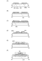
図1に、半導体装置の例として、トップゲート構造のスタガ型トランジスタ(順スタガ型
トランジスタともいう)の断面図及び平面図を示す。図1(A)は平面図であり、図1(
B)及び図1(C)は、図1(A)におけるA1−B1断面及びA2−B2断面に係る断
面図である。なお、図1(A)においては、第1のゲート絶縁膜402a、第2のゲート
絶縁膜402bを省略している。
FIG. 1 illustrates a cross-sectional view and a plan view of a staggered transistor (also referred to as a forward staggered transistor) having a top gate structure as an example of a semiconductor device. FIG. 1A is a plan view, and FIG.
B) and FIG. 1C are cross-sectional views of the A1-B1 cross section and the A2-B2 cross section in FIG. Note that in FIG. 1A, the first
図1(A)、図1(B)、及び図1(C)に示すトランジスタ410は、絶縁表面を有す
る基板400上に、絶縁膜406、ソース電極層405a、ドレイン電極層405b、酸
化物半導体膜403、第1のゲート絶縁膜402a、第2のゲート絶縁膜402b、及び
ゲート電極層401を含む。
A
なお、トランジスタ410上には、さらに絶縁物が設けられていても良い。また、ソース
電極層405aやドレイン電極層405bと配線とを電気的に接続させるために、第2の
ゲート絶縁膜402bなどには開口が形成されていても良い。また、酸化物半導体膜40
3の下方、絶縁膜406の下に、さらに、第2のゲート電極を有していても良い。
Note that an insulator may be further provided over the
2 and under the insulating
トランジスタ410において、酸化物半導体膜403と接する第1のゲート絶縁膜402
aをプラズマCVD法によりフッ化珪素及び酸素を含む成膜ガスを用いた酸化シリコン膜
で形成し、第1のゲート絶縁膜402a上に積層する第2のゲート絶縁膜402bを、プ
ラズマCVD法により水素化珪素及び酸素を含む成膜ガスを用いた酸化シリコン膜で形成
する。
In the
a is formed with a silicon oxide film using a deposition gas containing silicon fluoride and oxygen by a plasma CVD method, and a second
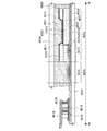
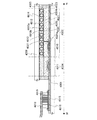
図2(A)乃至図2(F)にトランジスタ410の作製方法の一例を示す。
2A to 2F illustrate an example of a method for manufacturing the
まず、絶縁表面を有する基板400上に下地膜として機能する絶縁膜406を形成する。
First, the insulating
下地膜となる絶縁膜406は、基板400からの不純物元素の拡散を防止する機能があり
、プラズマCVD法又はスパッタリング法等により、酸化シリコン、窒化シリコン、酸化
窒化シリコン、窒化酸化シリコン、酸化アルミニウム、窒化アルミニウム、酸化窒化アル
ミニウム、窒化酸化アルミニウム、酸化ハフニウム、酸化ガリウム、又はこれらの混合材
料を用いて単層で又は積層して形成することができる。
The insulating
また、絶縁膜406は酸化物半導体膜403と接するので、プラズマCVD法により成膜
ガスに水素を含まない、フッ化珪素及び酸素を含む成膜ガスを用いた酸化シリコン膜で形
成してもよい。フッ化珪素としては四フッ化珪素(SiF4)、六フッ化二珪素(Si2
F6)などを用いることができる。また、絶縁膜406の成膜ガスに希ガス(ヘリウム、
アルゴンなど)を含ませてもよい。
Further, since the insulating
F 6 ) or the like can be used. Further, a rare gas (helium,
Argon, etc.) may be included.
プラズマCVD法によりフッ化珪素及び酸素を含む成膜ガスを用いて形成する絶縁膜40
6は、成膜ガスに水素を含まないので、酸化物半導体膜403へ混入することでトランジ
スタの特性変動の要因となる水素濃度を低く抑えた膜とすることができる。よって、絶縁
膜406は酸化物半導体膜403と接して設けられても、酸化物半導体膜403を水素で
汚染することなく、接して設けられることで他の膜より水素等の不純物が酸化物半導体膜
403へ混入することを防止することができる。
Insulating film 40 formed using a film forming gas containing silicon fluoride and oxygen by a plasma CVD method
No. 6 does not contain hydrogen in the deposition gas, so that it can be formed into a film in which the concentration of hydrogen that causes fluctuations in transistor characteristics is suppressed by being mixed into the
また、μ波(例えば周波数2.45GHz)を用いた高密度プラズマCVDは、緻密で絶
縁耐圧の高い高品質な絶縁膜を形成できるので、半導体装置に含まれる絶縁膜の形成に用
いると好ましい。
In addition, high-density plasma CVD using μ waves (for example, a frequency of 2.45 GHz) is preferably used for forming an insulating film included in a semiconductor device because a high-quality insulating film with high density and high withstand voltage can be formed.
絶縁表面を有する基板400に使用することができる基板に大きな制限はないが、少なく
とも、後の熱処理に耐えうる程度の耐熱性を有していることが必要となる。例えば、バリ
ウムホウケイ酸ガラスやアルミノホウケイ酸ガラスなどのガラス基板、セラミック基板、
石英基板、サファイア基板などを用いることができる。また、シリコンや炭化シリコンな
どの単結晶半導体基板、多結晶半導体基板、シリコンゲルマニウムなどの化合物半導体基
板、SOI基板などを適用することもでき、これらの基板上に半導体素子が設けられたも
のを、基板400として用いてもよい。
There is no particular limitation on a substrate that can be used as the
A quartz substrate, a sapphire substrate, or the like can be used. In addition, a single crystal semiconductor substrate such as silicon or silicon carbide, a polycrystalline semiconductor substrate, a compound semiconductor substrate such as silicon germanium, an SOI substrate, or the like can be applied, and a semiconductor element provided on these substrates, The
また、基板400として、可撓性基板を用いてもよい。可撓性基板を用いる場合、可撓性
基板上に酸化物半導体膜を含むトランジスタを直接作製してもよいし、他の作製基板に酸
化物半導体膜を含むトランジスタを作製し、その後可撓性基板に剥離、転置してもよい。
なお、作製基板から可撓性基板に剥離、転置するために、作製基板と酸化物半導体膜を含
むトランジスタとの間に剥離層を設けるとよい。
Further, a flexible substrate may be used as the
Note that in order to separate the transistor from the manufacturing substrate and transfer it to the flexible substrate, a separation layer may be provided between the manufacturing substrate and the transistor including the oxide semiconductor film.
次いで、絶縁膜406上に、ソース電極層405a及びドレイン電極層405b(これと
同じ層で形成される配線を含む)となる導電膜を形成する。ソース電極層405a、及び
ドレイン電極層405bに用いる導電膜としては、例えば、Al、Cr、Cu、Ta、T
i、Mo、Wからから選ばれた元素を含む金属膜、または上述した元素を成分とする金属
窒化物膜(窒化チタン膜、窒化モリブデン膜、窒化タングステン膜)等を用いることがで
きる。また、Al、Cuなどの金属膜の下側又は上側の一方または双方にTi、Mo、W
などの高融点金属膜またはそれらの金属窒化物膜(窒化チタン膜、窒化モリブデン膜、窒
化タングステン膜)を積層させた構成としても良い。また、ソース電極層、及びドレイン
電極層に用いる導電膜としては、導電性の金属酸化物で形成しても良い。導電性の金属酸
化物としては酸化インジウム(In2O3)、酸化スズ(SnO2)、酸化亜鉛(ZnO
)、酸化インジウム酸化スズ合金(In2O3―SnO2、ITOと略記する)、酸化イ
ンジウム酸化亜鉛合金(In2O3―ZnO)またはこれらの金属酸化物材料に酸化シリ
コンを含ませたものを用いることができる。
Next, a conductive film to be the
A metal film containing an element selected from i, Mo, and W, or a metal nitride film (a titanium nitride film, a molybdenum nitride film, or a tungsten nitride film) containing the above-described element as a component can be used. Also, Ti, Mo, W on one or both of the lower side or the upper side of a metal film such as Al, Cu, etc.
Alternatively, a high melting point metal film such as a metal nitride film (titanium nitride film, molybdenum nitride film, tungsten nitride film) may be stacked. The conductive film used for the source electrode layer and the drain electrode layer may be formed using a conductive metal oxide. Examples of the conductive metal oxide include indium oxide (In 2 O 3 ), tin oxide (SnO 2 ), and zinc oxide (ZnO).
), Indium oxide tin oxide alloy (In 2 O 3 —SnO 2 , abbreviated as ITO), indium oxide zinc oxide alloy (In 2 O 3 —ZnO), or these metal oxide materials containing silicon oxide Can be used.
第1のフォトリソグラフィ工程により導電膜上にレジストマスクを形成し、選択的にエッ
チングを行ってソース電極層405a、ドレイン電極層405bを形成した後、レジスト
マスクを除去する(図2(A)参照。)。
A resist mask is formed over the conductive film by a first photolithography step, and selective etching is performed to form a
なお、レジストマスクをインクジェット法で形成してもよい。レジストマスクをインクジ
ェット法で形成するとフォトマスクを使用しないため、製造コストを低減できる。
Note that the resist mask may be formed by an inkjet method. When the resist mask is formed by an ink-jet method, a manufacturing cost can be reduced because a photomask is not used.
また、絶縁膜406、ソース電極層405a、ドレイン電極層405b上に形成される酸
化物半導体膜に水素、水酸基及び水分がなるべく含まれないようにするために、酸化物半
導体膜の成膜の前処理として、スパッタリング装置の予備加熱室で、絶縁膜406が形成
された基板400、又はソース電極層405a、及びドレイン電極層405bまでが形成
された基板400を予備加熱し、基板400に吸着した水素、水分などの不純物を脱離し
排気することが好ましい。なお、予備加熱室に設ける排気手段はクライオポンプが好まし
い。なお、この予備加熱の処理は省略することもできる。
Further, in order to prevent the oxide semiconductor film formed over the insulating
次いで、絶縁膜406、ソース電極層405a、ドレイン電極層405b上に、膜厚2n
m以上200nm以下、好ましくは5nm以上30nm以下の酸化物半導体膜を形成する
。
Next, a film thickness of 2n is formed over the insulating
An oxide semiconductor film having a thickness of m to 200 nm, preferably 5 nm to 30 nm is formed.
酸化物半導体膜に用いる酸化物半導体としては、少なくともIn、Ga、Sn及びZnか
ら選ばれた一種以上の元素を含有する。例えば、四元系金属酸化物であるIn−Sn−G
a−Zn−O系酸化物半導体や、三元系金属酸化物であるIn−Ga−Zn−O系酸化物
半導体、In−Sn−Zn−O系酸化物半導体、In−Al−Zn−O系酸化物半導体、
Sn−Ga−Zn−O系酸化物半導体、Al−Ga−Zn−O系酸化物半導体、Sn−A
l−Zn−O系酸化物半導体や、二元系金属酸化物であるIn−Zn−O系酸化物半導体
、Sn−Zn−O系酸化物半導体、Al−Zn−O系酸化物半導体、Zn−Mg−O系酸
化物半導体、Sn−Mg−O系酸化物半導体、In−Mg−O系酸化物半導体や、In−
Ga−O系の材料、In−O系酸化物半導体、Sn−O系酸化物半導体、Zn−O系酸化
物半導体などを用いることができる。また、上記酸化物半導体にInとGaとSnとZn
以外の元素、例えばSiO2を含んでもよい。
An oxide semiconductor used for the oxide semiconductor film contains at least one element selected from In, Ga, Sn, and Zn. For example, In—Sn—G, which is a quaternary metal oxide
a-Zn-O-based oxide semiconductors, In-Ga-Zn-O-based oxide semiconductors that are ternary metal oxides, In-Sn-Zn-O-based oxide semiconductors, In-Al-Zn-O Oxide semiconductors,
Sn-Ga-Zn-O-based oxide semiconductor, Al-Ga-Zn-O-based oxide semiconductor, Sn-A
l-Zn-O-based oxide semiconductor, binary metal oxide In-Zn-O-based oxide semiconductor, Sn-Zn-O-based oxide semiconductor, Al-Zn-O-based oxide semiconductor, Zn -Mg-O-based oxide semiconductor, Sn-Mg-O-based oxide semiconductor, In-Mg-O-based oxide semiconductor, In-
A Ga—O-based material, an In—O-based oxide semiconductor, a Sn—O-based oxide semiconductor, a Zn—O-based oxide semiconductor, or the like can be used. In addition, the oxide semiconductor includes In, Ga, Sn, and Zn.
Other elements such as SiO 2 may be included.
例えば、In−Ga−Zn−O系酸化物半導体とは、インジウム(In)、ガリウム(G
a)、亜鉛(Zn)を有する酸化物半導体、という意味であり、その組成比は問わない。
For example, an In—Ga—Zn—O-based oxide semiconductor includes indium (In) and gallium (G
a), an oxide semiconductor having zinc (Zn), and the composition ratio is not limited.
また、酸化物半導体膜は、化学式InMO3(ZnO)m(m>0)で表記される薄膜を
用いることができる。ここで、Mは、Ga、Al、MnおよびCoから選ばれた一または
複数の金属元素を示す。例えばMとして、Ga、Ga及びAl、Ga及びMn、またはG
a及びCoなどがある。
As the oxide semiconductor film, a thin film represented by the chemical formula, InMO 3 (ZnO) m (m> 0) can be used. Here, M represents one or more metal elements selected from Ga, Al, Mn, and Co. For example, as M, Ga, Ga and Al, Ga and Mn, or G
a and Co.
酸化物半導体膜に用いる酸化物半導体としては、インジウムを含む酸化物半導体、インジ
ウム及びガリウムを含む酸化物半導体などを好適に用いることができる。
As the oxide semiconductor used for the oxide semiconductor film, an oxide semiconductor containing indium, an oxide semiconductor containing indium and gallium, or the like can be preferably used.
本実施の形態では、酸化物半導体膜としてIn−Ga−Zn−O系酸化物ターゲットを用
いてスパッタリング法により成膜する。また、酸化物半導体膜は、希ガス(代表的にはア
ルゴン)雰囲気下、酸素雰囲気下、又は希ガスと酸素の混合雰囲気下においてスパッタリ
ング法により形成することができる。
In this embodiment, the oxide semiconductor film is formed by a sputtering method using an In—Ga—Zn—O-based oxide target. The oxide semiconductor film can be formed by a sputtering method in a rare gas (typically argon) atmosphere, an oxygen atmosphere, or a mixed atmosphere of a rare gas and oxygen.
また、酸化物半導体としてIn−Zn−O系の材料を用いる場合、用いるターゲットとし
ては、原子数比で、In:Zn=50:1〜1:2(モル数比に換算するとIn2O3:
ZnO=25:1〜1:4)、好ましくはIn:Zn=20:1〜1:1(モル数比に換
算するとIn2O3:ZnO=10:1〜1:2)、さらに好ましくはIn:Zn=15
:1〜1.5:1(モル数比に換算するとIn2O3:ZnO=15:2〜3:4)とす
る。例えば、In−Zn−O系酸化物半導体の形成に用いるターゲットは、原子数比がI
n:Zn:O=X:Y:Zのとき、Z>1.5X+Yとする。
In the case where an In—Zn—O-based material is used as the oxide semiconductor, the target to be used is an atomic ratio of In: Zn = 50: 1 to 1: 2 (in 2 O 3 when converted to a molar ratio). :
ZnO = 25: 1 to 1: 4), preferably In: Zn = 20: 1 to 1: 1 (In 2 O 3 : ZnO = 10: 1 to 1: 2 in terms of molar ratio), more preferably In: Zn = 15
: 1 to 1.5: 1 (In 2 O 3 : ZnO = 15: 2 to 3: 4 when converted to a molar ratio). For example, a target used for forming an In—Zn—O-based oxide semiconductor has an atomic ratio of I
When n: Zn: O = X: Y: Z, Z> 1.5X + Y.
また、酸化物ターゲットの充填率は90%以上100%以下、好ましくは95%以上99
.9%以下である。充填率の高い金属酸化物ターゲットを用いることにより、成膜した酸
化物半導体膜は緻密な膜とすることができる。
The filling rate of the oxide target is 90% to 100%, preferably 95% to 99%.
. 9% or less. By using a metal oxide target with a high filling rate, the formed oxide semiconductor film can be a dense film.
酸化物半導体膜を成膜する際に用いるスパッタリングガスは、水素、水、水酸基又は水素
化物などの不純物が除去された高純度ガスを用いることが好ましい。
As a sputtering gas used for forming the oxide semiconductor film, a high-purity gas from which impurities such as hydrogen, water, a hydroxyl group, or hydride are removed is preferably used.
減圧状態に保持された成膜室内に基板を保持し、基板温度を100℃以上600℃以下好
ましくは200℃以上400℃以下とする。基板を加熱しながら成膜することにより、成
膜した酸化物半導体膜に含まれる不純物濃度を低減することができる。また、スパッタリ
ングによる損傷が軽減される。そして、成膜室内の残留水分を除去しつつ水素及び水分が
除去されたスパッタリングガスを導入し、上記ターゲットを用いて基板400上に酸化物
半導体膜を成膜する。成膜室内の残留水分を除去するためには、吸着型の真空ポンプ、例
えば、クライオポンプ、イオンポンプ、チタンサブリメーションポンプを用いることが好
ましい。また、排気手段としては、ターボ分子ポンプにコールドトラップを加えたもので
あってもよい。クライオポンプを用いて排気した成膜室は、例えば、水素原子、水など水
素原子を含む化合物(より好ましくは炭素原子を含む化合物も)等が排気されるため、当
該成膜室で成膜した酸化物半導体膜に含まれる不純物の濃度を低減できる。
The substrate is held in a deposition chamber kept under reduced pressure, and the substrate temperature is set to 100 ° C. to 600 ° C., preferably 200 ° C. to 400 ° C. By forming the film while heating the substrate, the concentration of impurities contained in the formed oxide semiconductor film can be reduced. Further, damage due to sputtering is reduced. Then, a sputtering gas from which hydrogen and moisture are removed is introduced while moisture remaining in the deposition chamber is removed, and an oxide semiconductor film is formed over the
成膜条件の一例としては、基板とターゲットの間との距離を100mm、圧力0.6Pa
、直流(DC)電源0.5kW、酸素(酸素流量比率100%)雰囲気下の条件が適用さ
れる。なお、パルス直流電源を用いると、成膜時に発生する粉状物質(パーティクル、ご
みともいう)が軽減でき、膜厚分布も均一となるために好ましい。
As an example of film formation conditions, the distance between the substrate and the target is 100 mm, and the pressure is 0.6 Pa.
A condition under a direct current (DC) power supply of 0.5 kW and an oxygen (
次いで、酸化物半導体膜に熱処理を行う。この熱処理によって過剰な水素(水や水酸基を
含む)を除去(脱水化または脱水素化)し、酸化物半導体膜の構造を整え、エネルギーギ
ャップ中の欠陥準位を低減することができる。熱処理の温度は、250℃以上750℃以
下、または400℃以上基板の歪み点未満とする。ここでは、熱処理装置の一つである電
気炉に基板を導入し、酸化物半導体膜に対して窒素雰囲気下450℃において1時間の熱
処理を行った後、大気に触れることなく、酸化物半導体膜への水や水素の再混入を防ぎ、
酸化物半導体膜441を得る(図2(B)参照。)。
Next, heat treatment is performed on the oxide semiconductor film. By this heat treatment, excess hydrogen (including water and hydroxyl groups) can be removed (dehydration or dehydrogenation), the structure of the oxide semiconductor film can be adjusted, and the defect level in the energy gap can be reduced. The heat treatment temperature is 250 ° C. or higher and 750 ° C. or lower, or 400 ° C. or higher and lower than the strain point of the substrate. Here, a substrate is introduced into an electric furnace which is one of heat treatment apparatuses, and the oxide semiconductor film is subjected to heat treatment at 450 ° C. for 1 hour in a nitrogen atmosphere, and then the oxide semiconductor film is not exposed to the air. Prevents re-mixing of water and hydrogen into the
An
なお、熱処理装置は電気炉に限られず、抵抗発熱体などの発熱体からの熱伝導または熱輻
射によって、被処理物を加熱する装置を用いてもよい。例えば、GRTA(Gas Ra
pid Thermal Anneal)装置、LRTA(Lamp Rapid Th
ermal Anneal)装置等のRTA(Rapid Thermal Annea
l)装置を用いることができる。LRTA装置は、ハロゲンランプ、メタルハライドラン
プ、キセノンアークランプ、カーボンアークランプ、高圧ナトリウムランプ、高圧水銀ラ
ンプなどのランプから発する光(電磁波)の輻射により、被処理物を加熱する装置である
。GRTA装置は、高温のガスを用いて熱処理を行う装置である。高温のガスには、アル
ゴンなどの希ガス、または窒素のような、熱処理によって被処理物と反応しない不活性気
体が用いられる。
Note that the heat treatment apparatus is not limited to an electric furnace, and an apparatus for heating an object to be processed by heat conduction or heat radiation from a heating element such as a resistance heating element may be used. For example, GRTA (Gas Ra
pid Thermal Anneal) device, LRTA (Lamp Rapid Th
RTA (Rapid Thermal Annea)
l) An apparatus can be used. The LRTA apparatus is an apparatus that heats an object to be processed by radiation of light (electromagnetic waves) emitted from a lamp such as a halogen lamp, a metal halide lamp, a xenon arc lamp, a carbon arc lamp, a high pressure sodium lamp, or a high pressure mercury lamp. The GRTA apparatus is an apparatus that performs heat treatment using a high-temperature gas. As the high-temperature gas, an inert gas that does not react with an object to be processed by heat treatment, such as nitrogen or a rare gas such as argon, is used.
例えば、熱処理として、650℃以上700℃以下の高温に加熱した不活性ガス中に基板
を移動させて入れ、数分間加熱した後、基板を移動させて高温に加熱した不活性ガス中か
ら出すGRTAを行ってもよい。
For example, as a heat treatment, the substrate is moved into an inert gas heated to a high temperature of 650 ° C. or higher and 700 ° C. or lower, heated for several minutes, and then moved from the inert gas heated to a high temperature by moving the substrate. May be performed.
なお、熱処理においては、窒素、またはヘリウム、ネオン、アルゴン等の希ガスに、水、
水素などが含まれないことが好ましい。または、熱処理装置に導入する窒素、またはヘリ
ウム、ネオン、アルゴン等の希ガスの純度を、6N(99.9999%)以上好ましくは
7N(99.99999%)以上(即ち不純物濃度を1ppm以下、好ましくは0.1p
pm以下)とすることが好ましい。
Note that in the heat treatment, nitrogen, a rare gas such as helium, neon, or argon, water,
It is preferable that hydrogen and the like are not contained. Alternatively, the purity of nitrogen or a rare gas such as helium, neon, or argon introduced into the heat treatment apparatus is 6N (99.9999%) or more, preferably 7N (99.99999%) or more (that is, the impurity concentration is 1 ppm or less, preferably Is 0.1p
pm or less).
また、熱処理で酸化物半導体膜を加熱した後、同じ炉に高純度の酸素ガス、高純度の一酸
化二窒素ガス、又は超乾燥エア(CRDS(キャビティリングダウンレーザー分光法)方
式の露点計を用いて測定した場合の水分量が20ppm(露点換算で−55℃)以下、好
ましくは1ppm以下、好ましくは10ppb以下の空気)を導入してもよい。酸素ガス
または一酸化二窒素ガスに、水、水素などが含まれないことが好ましい。または、熱処理
装置に導入する酸素ガスまたは一酸化二窒素ガスの純度を、6N以上好ましくは7N以上
(即ち、酸素ガスまたは一酸化二窒素ガス中の不純物濃度を1ppm以下、好ましくは0
.1ppm以下)とすることが好ましい。酸素ガス又は一酸化二窒素ガスの作用により、
脱水化または脱水素化処理による不純物の排除工程によって同時に減少してしまった酸化
物半導体を構成する主成分材料である酸素を供給することによって、酸化物半導体膜を高
純度化及び電気的にi型(真性)化する。
After heating the oxide semiconductor film by heat treatment, a high-purity oxygen gas, high-purity dinitrogen monoxide gas, or ultra-dry air (CRDS (cavity ring-down laser spectroscopy) type dew point meter) is installed in the same furnace. The amount of water when measured by use may be 20 ppm (air at dew point conversion of −55 ° C.) or less, preferably 1 ppm or less, preferably 10 ppb or less. It is preferable that water, hydrogen, and the like are not contained in the oxygen gas or the dinitrogen monoxide gas. Alternatively, the purity of the oxygen gas or nitrous oxide introduced into the heat treatment apparatus is 6 N or more, preferably 7 N or more (that is, the impurity concentration in the oxygen gas or nitrous oxide is 1 ppm or less, preferably 0
. 1 ppm or less). By the action of oxygen gas or nitrous oxide gas,
By supplying oxygen, which is a main component material of the oxide semiconductor, which has been simultaneously reduced by the impurity removal step by dehydration or dehydrogenation treatment, the oxide semiconductor film is highly purified and electrically i. Make type (intrinsic).
また、酸化物半導体膜の熱処理は、島状の酸化物半導体膜に加工した後の酸化物半導体膜
に行うこともできる。また、熱処理は、酸化物半導体膜成膜後であれば、島状の酸化物半
導体膜上に第1のゲート絶縁膜、及び/又は第2のゲート絶縁膜を積層させた後で行って
も良い。
The heat treatment of the oxide semiconductor film can be performed on the oxide semiconductor film that has been processed into the island-shaped oxide semiconductor film. Further, the heat treatment may be performed after the first gate insulating film and / or the second gate insulating film are stacked over the island-shaped oxide semiconductor film as long as the oxide semiconductor film is formed. good.
脱水化または脱水素化された酸化物半導体膜441に酸素ドープ処理を行ってもよい。酸
化物半導体膜441に酸素ドープ処理を行うことにより、酸素を酸化物半導体膜441に
供給して、酸化物半導体膜441中、又は酸化物半導体膜441中及び該界面近傍に酸素
を含有させることができる。
The
なお、酸素ドープ処理とは、酸素ラジカルまたは酸素原子、酸素イオンを酸化物半導体膜
の表面及びバルクへ添加することである。特に、酸素をプラズマ化することにより、上記
酸素ラジカルまたは酸素原子、酸素イオンを酸化物半導体膜の表面及びバルク中に添加す
ることを酸素プラズマドープ処理ともいう。なお、酸化物半導体膜が形成される基板にバ
イアスを印加すると好ましい。
Note that the oxygen doping treatment refers to adding oxygen radicals, oxygen atoms, or oxygen ions to the surface and bulk of the oxide semiconductor film. In particular, adding oxygen radicals, oxygen atoms, or oxygen ions to the surface and bulk of the oxide semiconductor film by turning oxygen into plasma is also referred to as oxygen plasma doping treatment. Note that a bias is preferably applied to the substrate over which the oxide semiconductor film is formed.
本明細書に開示する酸化物半導体膜を有するトランジスタの作製工程において、酸素ドー
プ処理を行うことによって、積層する絶縁膜の膜中(バルク中)、酸化物半導体膜の膜中
(バルク中)、ゲート絶縁膜の膜中(バルク中)、ゲート絶縁膜と酸化物半導体膜の界面
、酸化物半導体膜と絶縁膜との界面において、少なくとも1ヶ所以上、該膜の化学量論比
をこえる酸素が存在する酸素過剰領域を設けることができる。
In the manufacturing process of the transistor including an oxide semiconductor film disclosed in this specification, by performing oxygen doping treatment, in the insulating film to be stacked (in the bulk), in the oxide semiconductor film (in the bulk), In the gate insulating film (in the bulk), at the interface between the gate insulating film and the oxide semiconductor film, or at the interface between the oxide semiconductor film and the insulating film, oxygen exceeding the stoichiometric ratio of the film An existing oxygen-excess region can be provided.
また、上記酸素過剰領域を、積層する絶縁膜、酸化物半導体膜、及びゲート絶縁膜におい
て2ヶ所以上に設けてもよい。例えば作製工程において、酸素ドープ処理を行うことによ
って、ゲート絶縁膜と酸化物半導体膜の界面、酸化物半導体膜の膜中(バルク中)、及び
酸化物半導体膜と絶縁膜との界面にそれぞれ酸素過剰領域を設けることができる。
The oxygen-excess region may be provided in two or more places in the insulating film, the oxide semiconductor film, and the gate insulating film to be stacked. For example, by performing oxygen doping treatment in the manufacturing process, oxygen is added to the interface between the gate insulating film and the oxide semiconductor film, the oxide semiconductor film (in the bulk), and the interface between the oxide semiconductor film and the insulating film. An excess region can be provided.
ドープされる酸素(酸素ラジカル、酸素原子、及び/又は酸素イオン)は、酸素を含むガ
スを用いてプラズマ発生装置により供給されてもよいし、又はオゾン発生装置により供給
されてもよい。より具体的には、例えば、半導体装置の作製工程において用いるエッチン
グ処理を行うための装置や、レジストマスクに対してアッシングを行うための装置などを
用いて酸素を発生させ、酸化物半導体膜441を処理することができる。
Doped oxygen (oxygen radicals, oxygen atoms, and / or oxygen ions) may be supplied by a plasma generator using a gas containing oxygen, or may be supplied by an ozone generator. More specifically, for example, oxygen is generated using an apparatus for performing an etching process used in a manufacturing process of a semiconductor device or an apparatus for performing ashing on a resist mask, so that the
また、酸素ドープ処理を行った酸化物半導体膜441に熱処理(温度150℃以上470
℃以下)を行ってもよい。熱処理は、窒素、酸素、超乾燥空気(CRDS(キャビティリ
ングダウンレーザー分光法)方式の露点計を用いて測定した場合の水分量が20ppm(
露点換算で−55℃)以下、好ましくは1ppm以下、より好ましくは10ppb以下の
空気)、または希ガス(アルゴン、ヘリウムなど)の雰囲気下で行えばよいが、上記窒素
、酸素、超乾燥空気、または希ガス等の雰囲気は、水、水素などが含まれず高純度化され
ていることが好ましい。
Further, the
C. or less) may be performed. The heat treatment is performed using nitrogen, oxygen, and ultra-dry air (CRDS (cavity ring down laser spectroscopy) type dew point meter) when the moisture content is 20 ppm (
(Dew point conversion: −55 ° C.) or less, preferably 1 ppm or less, more preferably 10 ppb or less, or a rare gas (argon, helium, etc.) atmosphere. Alternatively, the atmosphere such as a rare gas is preferably highly purified without containing water or hydrogen.
以上の工程で高純度化し、電気的にi型(真性)化された酸化物半導体膜441を得る。
高純度化された酸化物半導体膜441中にはキャリアが極めて少ない(ゼロに近い)。
Through the above steps, an
There are very few carriers (close to zero) in the highly purified
次いで、酸化物半導体膜441上に第1のゲート絶縁膜443を形成する(図2(C)参
照。)。第1のゲート絶縁膜443は、プラズマCVD法により水素を含まないフッ化珪
素及び酸素を含む成膜ガスを用いた酸化シリコン膜で形成する。フッ化珪素としては四フ
ッ化珪素(SiF4)、六フッ化二珪素(Si2F6)などを用いることができる。また
、第1のゲート絶縁膜443の成膜ガスに希ガス(ヘリウム、アルゴンなど)を含ませて
もよい。
Next, a first
プラズマCVD法によりフッ化珪素及び酸素を含む成膜ガスを用いて形成する第1のゲー
ト絶縁膜443は、酸化物半導体膜403へ混入することでトランジスタの特性変動の要
因となる水素を成膜ガスに含まないので、水素濃度を低く抑えた膜とすることができる。
よって、第1のゲート絶縁膜443は酸化物半導体膜403と接して設けられても、酸化
物半導体膜403を水素で汚染することなく、接して設けられることで他の膜より水素等
の不純物が酸化物半導体膜403へ混入することを防止することができる。
The first
Therefore, even when the first
本実施の形態では、第1のゲート絶縁膜443を、プラズマCVD法により四フッ化珪素
(SiF4)、一酸化二窒素(N2O)及びアルゴン(Ar)を含む成膜ガスを用いて形
成する。例えば、第1のゲート絶縁膜443の成膜条件としては、成膜ガスとしては四フ
ッ化珪素(SiF4)、一酸化二窒素(N2O)、及びアルゴン(Ar)(SiF4:N
2O:Ar=6sccm:1000sccm:1000sccm)を用い、チャンバー内
の圧力は133Pa、電力は800W、電源周波数は60MHz、基板(シリコンウエハ
)の温度は400℃とすればよい。
In this embodiment, the first
2 O: Ar = 6 sccm: 1000 sccm: 1000 sccm), the pressure in the chamber is 133 Pa, the power is 800 W, the power frequency is 60 MHz, and the temperature of the substrate (silicon wafer) is 400 ° C.
よって、第1のゲート絶縁膜443はフッ素を含む酸化シリコン膜となる。成膜ガスとし
てフッ化珪素及び酸素を用いて形成した第1のゲート絶縁膜443では、フッ素濃度より
水素濃度の方が低く、好ましくはフッ素濃度は1×10²⁰ atoms/cm3以上で
あり、水素濃度は1×10²⁰ atoms/cm3未満である。第1のゲート絶縁膜4
43の膜厚は1nm以上10nm以下程度とすればよい。
Therefore, the first
The film thickness of 43 may be about 1 nm to 10 nm.
なお、第1のゲート絶縁膜443は、ソース電極層405a及びドレイン電極層405b
を酸化物半導体膜441が覆った状態で酸化物半導体膜441上に形成されるため、ソー
ス電極層405a及びドレイン電極層405bは、第1のゲート絶縁膜443成膜時に用
いるフッ化珪素及び酸素を含む成膜ガスに曝されず、腐蝕などの損傷を受けない。
Note that the first
Is formed over the
次いで、酸化物半導体膜441及び第1のゲート絶縁膜443を第2のフォトリソグラフ
ィ工程により島状の酸化物半導体膜403、及び島状の第1のゲート絶縁膜402aに加
工する(図2(D)参照。)。また、島状の酸化物半導体膜441、及び島状の第1のゲ
ート絶縁膜402aを形成するためのレジストマスクをインクジェット法で形成してもよ
い。レジストマスクをインクジェット法で形成するとフォトマスクを使用しないため、製
造コストを低減できる。
Next, the
なお、ここでの酸化物半導体膜のエッチングは、ドライエッチングでもウェットエッチン
グでもよく、両方を用いてもよい。例えば、第1のゲート絶縁膜443をドライエッチン
グにより加工し、第1のゲート絶縁膜402aをマスクとして酸化物半導体膜441をウ
ェットエッチングによって加工してもよい。第1のゲート絶縁膜443のエッチングガス
としては、塩素を含むガス(塩素系ガス、例えば塩素(Cl2)、三塩化硼素(BCl3
)、四塩化珪素(SiCl4)、四塩化炭素(CCl4)など)、または、フッ素を含む
ガス(フッ素系ガス、例えば四フッ化炭素(CF4)、六フッ化硫黄(SF6)、三フッ
化窒素(NF3)、トリフルオロメタン(CHF3)など)を用いることができる。さら
に上記ガスに酸素や希ガス(例えばArなど)を添加したエッチングガスを用いてもよい
。酸化物半導体膜のウェットエッチングに用いるエッチング液としては、燐酸と酢酸と硝
酸を混ぜた溶液などを用いることができる。また、ITO07N(関東化学社製)を用い
てもよい。
Note that the etching of the oxide semiconductor film here may be either dry etching or wet etching, or both. For example, the first
), Silicon tetrachloride (SiCl 4 ), carbon tetrachloride (CCl 4 ), etc., or a gas containing fluorine (fluorine-based gas such as carbon tetrafluoride (CF 4 ), sulfur hexafluoride (SF 6 ), Nitrogen trifluoride (NF 3 ), trifluoromethane (CHF 3 ), or the like can be used. Further, an etching gas in which oxygen or a rare gas (eg, Ar) is added to the above gas may be used. As an etchant used for wet etching of the oxide semiconductor film, a mixed solution of phosphoric acid, acetic acid, and nitric acid, or the like can be used. In addition, ITO07N (manufactured by Kanto Chemical Co., Inc.) may be used.
酸化物半導体膜441及び第1のゲート絶縁膜443のエッチング加工を同じマスクで行
うと、島状の酸化物半導体膜403、及び島状の第1のゲート絶縁膜402aを同形状に
加工することができ、図2(D)のように端部を一致させることができる。
When the
次に、絶縁膜406、ソース電極層405a、ドレイン電極層405b、酸化物半導体膜
403、及び第1のゲート絶縁膜402a上に第2のゲート絶縁膜402bを形成する(
図2(E)参照。)。第2のゲート絶縁膜402bは、プラズマCVD法により水素化珪
素及び酸素を含む成膜ガスを用いた酸化シリコン膜で形成する。水素化珪素としては四水
素化珪素(モノシラン:SiH4)、六水素化珪素(ジシラン:Si2H6)、八水素化
珪素(トリシラン:Si3H8)などを用いることができる。また、第2のゲート絶縁膜
402bの成膜ガスに希ガス(ヘリウム、アルゴンなど)を含ませてもよい。
Next, the second
Refer to FIG. ). The second
本実施の形態では、第2のゲート絶縁膜402bを、プラズマCVD法により水素化珪素
(SiH4)及び一酸化二窒素(N2O)を含む成膜ガスを用いて形成する。例えば、第
2のゲート絶縁膜402bの成膜条件としては、成膜ガスとしては四水素化珪素(SiH
4)及び一酸化二窒素(N2O)(SiH4:N2O=4sccm:800sccm)を
用い、チャンバー内の圧力は40Pa、電力は150W、電源周波数は60MHz、基板
(シリコンウエハ)の温度は400℃とすればよい。
In this embodiment, the second
4 ) and dinitrogen monoxide (N 2 O) (SiH 4 : N 2 O = 4 sccm: 800 sccm), the pressure in the chamber is 40 Pa, the power is 150 W, the power frequency is 60 MHz, the temperature of the substrate (silicon wafer) May be 400 ° C.
よって、第2のゲート絶縁膜402bは第1のゲート絶縁膜402aと比較してより高濃
度の水素を含む酸化シリコン膜となる。成膜ガスとして水素化珪素及び酸素を用いて形成
した第2のゲート絶縁膜402bでは、フッ素濃度より水素濃度の方が高く、好ましくは
フッ素濃度は1×10²⁰ atoms/cm3未満であり、水素濃度は1×1020
atoms/cm3以上である。第2のゲート絶縁膜402bの膜厚は50nm以上10
0nm以下程度とすればよい。
Therefore, the second
atoms / cm 3 or more. The thickness of the second
What is necessary is just to be about 0 nm or less.
プラズマCVD法によりフッ化珪素及び酸素を含む成膜ガスを用いて形成すると、第1の
ゲート絶縁膜402aを緻密な膜とすることができる。緻密性が高い第1のゲート絶縁膜
402aによって、積層する第2のゲート絶縁膜402bに含まれる水素が酸化物半導体
膜中に侵入するのを防止することができる。
When a film formation gas containing silicon fluoride and oxygen is formed by a plasma CVD method, the first
ソース電極層405a、ドレイン電極層405b、第1のゲート絶縁膜402a上に接し
て形成される第2のゲート絶縁膜402bは、プラズマCVD法により水素化珪素及び酸
素を含む成膜ガスを用いて形成するため比較的速い成膜速度で成膜することができるので
、第1のゲート絶縁膜402aより厚膜化が可能であり、生産性に有利である。また、接
して形成するソース電極層405a、ドレイン電極層405bを腐蝕するフッ素や塩素な
どを成膜ガスに用いないために、ソース電極層405a、ドレイン電極層405b表面を
あらすことなく第2のゲート絶縁膜402bを形成することができる。
The
従って半導体装置の作製工程において、ソース電極層405a、ドレイン電極層405b
の腐蝕による形状不良や、積層する第2のゲート絶縁膜402bの被覆不良などを防止し
、信頼性の高い半導体装置を歩留まり良く作製することができる。
Therefore, in the manufacturing process of the semiconductor device, the
Thus, a highly reliable semiconductor device can be manufactured with high yield by preventing a shape defect due to corrosion and a covering defect of the second
第2のゲート絶縁膜402b上に導電膜を形成した後、第3のフォトリソグラフィ工程に
よりゲート電極層401を形成する。
After a conductive film is formed over the second
ゲート電極層401は、プラズマCVD法又はスパッタリング法等により、モリブデン、
チタン、タンタル、タングステン、アルミニウム、銅、ネオジム、スカンジウム等の金属
材料又はこれらを主成分とする合金材料を用いて、単層で又は積層して形成することがで
きる。
The
A single layer or a stacked layer can be formed using a metal material such as titanium, tantalum, tungsten, aluminum, copper, neodymium, or scandium or an alloy material containing these as a main component.
以上の工程でトランジスタ410が形成される(図2(F)参照。)。トランジスタ41
0は、トランジスタの特性変動の要因となる水素、水分、水酸基又は水素化物(水素化合
物ともいう)などの不純物を酸化物半導体膜より意図的に排除し、かつ酸素を供給される
ことで高純度化された酸化物半導体膜403を含むトランジスタであり、酸化物半導体膜
403に接する第1のゲート絶縁膜402aの水素濃度は低く制御されている。よって、
トランジスタ410は、電気的特性変動が抑制されており、電気的に安定である。
Through the above steps, the
0 has high purity by intentionally removing impurities such as hydrogen, moisture, hydroxyl groups, or hydrides (also referred to as hydrogen compounds) that cause transistor characteristic fluctuations from the oxide semiconductor film and being supplied with oxygen. In the transistor including the oxidized
The
また、図3(A)のように絶縁膜406を第1の絶縁膜406a、第2の絶縁膜406b
と積層構造とし、酸化物半導体膜403と接する第2の絶縁膜406bを第1のゲート絶
縁膜402aと同様に成膜ガスに水素を含まない、プラズマCVD法によりフッ化珪素及
び酸素を含む成膜ガスを用いた酸化シリコン膜で形成してもよい。この場合、第1の絶縁
膜406aとして窒化シリコン膜や窒化酸化シリコン膜などの緻密な窒化膜を用いて、基
板400からの不純物の混入を防止する構成としてもよい。
In addition, as illustrated in FIG. 3A, the insulating
As in the first
また、図3(B)のようにゲート電極層401上にトランジスタ410を覆う保護膜とし
て絶縁膜407を設けてもよい。
Further, as illustrated in FIG. 3B, an insulating
絶縁膜407は、プラズマCVD法又はスパッタリング法等により、酸化シリコン、窒化
シリコン、酸化窒化シリコン、窒化酸化シリコン、酸化アルミニウム、窒化アルミニウム
、酸化窒化アルミニウム、窒化酸化アルミニウム、酸化ハフニウム、酸化ガリウム、又は
これらの混合材料を用いて単層で又は積層して形成することができる。
The insulating
上述の絶縁膜407の形成後には、熱処理を行ってもよい。熱処理の温度は、250℃以
上700℃以下、好ましくは450℃以上600℃以下、または基板の歪み点未満とする
。
Heat treatment may be performed after the above-described
熱処理は、窒素、酸素、超乾燥空気(CRDS(キャビティリングダウンレーザー分光法
)方式の露点計を用いて測定した場合の水分量が20ppm(露点換算で−55℃)以下
、好ましくは1ppm以下、より好ましくは10ppb以下の空気)、または希ガス(ア
ルゴン、ヘリウムなど)の雰囲気下で行えばよいが、上記窒素、酸素、超乾燥空気、また
は希ガス等の雰囲気には、水、水素などが含まれないことが好ましい。また、熱処理装置
に導入する窒素、酸素、または希ガスの純度は、6N(99.9999%)以上(即ち不
純物濃度を1ppm以下)とするのが好ましく、7N(99.99999%)以上(即ち
不純物濃度を0.1ppm以下)とすると、より好ましい。
The heat treatment is performed by using nitrogen, oxygen, and ultra-dry air (CRDS (cavity ring-down laser spectroscopy) type dew point meter) when the moisture content is 20 ppm (-55 ° C. in terms of dew point) or less, preferably 1 ppm or less. More preferably, it may be performed in an atmosphere of 10 ppb or less) or a rare gas (argon, helium, etc.). In the atmosphere of nitrogen, oxygen, ultra-dry air, or rare gas, water, hydrogen, etc. It is preferably not included. The purity of nitrogen, oxygen, or a rare gas introduced into the heat treatment apparatus is preferably 6N (99.9999%) or higher (that is, the impurity concentration is 1 ppm or lower), and 7N (99.99999%) or higher (that is, More preferably, the impurity concentration is 0.1 ppm or less.
本実施の形態を用いて作製した、高純度化された酸化物半導体膜403を用いたトランジ
スタ410は、オフ状態における電流値(オフ電流値)を低くすることができる。
The
また、酸化物半導体膜403を用いたトランジスタ410は、比較的高い電界効果移動度
が得られるため、高速駆動が可能である。よって、表示機能を有する半導体装置の画素部
に上記トランジスタを用いることで、高画質な画像を提供することができる。また、高純
度化された酸化物半導体膜を含むトランジスタによって、同一基板上に駆動回路部または
画素部を作り分けて作製することができるため、半導体装置の部品点数を削減することが
できる。
In addition, the
以上のように、安定した電気的特性を有する酸化物半導体を用いた半導体装置を提供する
ことができる。よって、信頼性の高い半導体装置を提供することができる。
As described above, a semiconductor device including an oxide semiconductor having stable electrical characteristics can be provided. Therefore, a highly reliable semiconductor device can be provided.
(実施の形態2)
実施の形態1で一例を示したトランジスタを用いて表示機能を有する半導体装置(表示装
置ともいう)を作製することができる。また、トランジスタを含む駆動回路の一部または
全体を、画素部と同じ基板上に一体形成し、システムオンパネルを形成することができる
。
(Embodiment 2)
A semiconductor device having a display function (also referred to as a display device) can be manufactured using the transistor described as an example in Embodiment 1. In addition, part or the whole of a driver circuit including a transistor can be formed over the same substrate as the pixel portion to form a system-on-panel.
図10(A)において、第1の基板4001上に設けられた画素部4002を囲むように
して、シール材4005が設けられ、第2の基板4006によって封止されている。図1
0(A)においては、第1の基板4001上のシール材4005によって囲まれている領
域とは異なる領域に、別途用意された基板上に単結晶半導体膜又は多結晶半導体膜で形成
された走査線駆動回路4004、信号線駆動回路4003が実装されている。また別途形
成された信号線駆動回路4003と、走査線駆動回路4004または画素部4002に与
えられる各種信号及び電位は、FPC(Flexible printed circu
it)4018a、4018bから供給されている。
In FIG. 10A, a
In 0 (A), a scan formed using a single crystal semiconductor film or a polycrystalline semiconductor film over a separately prepared substrate in a region different from the region surrounded by the
it) is supplied from 4018a and 4018b.
図10(B)及び図10(C)において、第1の基板4001上に設けられた画素部40
02と、走査線駆動回路4004とを囲むようにして、シール材4005が設けられてい
る。また画素部4002と、走査線駆動回路4004の上に第2の基板4006が設けら
れている。よって画素部4002と、走査線駆動回路4004とは、第1の基板4001
とシール材4005と第2の基板4006とによって、表示素子と共に封止されている。
図10(B)及び図10(C)においては、第1の基板4001上のシール材4005に
よって囲まれている領域とは異なる領域に、別途用意された基板上に単結晶半導体膜又は
多結晶半導体膜で形成された信号線駆動回路4003が実装されている。図10(B)及
び図10(C)においては、別途形成された信号線駆動回路4003と、走査線駆動回路
4004または画素部4002に与えられる各種信号及び電位は、FPC4018から供
給されている。
10B and 10C, the pixel portion 40 provided over the
02 and the scanning
And the
10B and 10C, a single crystal semiconductor film or a polycrystal is formed over a separately prepared substrate in a region different from the region surrounded by the
また図10(B)及び図10(C)においては、信号線駆動回路4003を別途形成し、
第1の基板4001に実装している例を示しているが、この構成に限定されない。走査線
駆動回路を別途形成して実装しても良いし、信号線駆動回路の一部または走査線駆動回路
の一部のみを別途形成して実装しても良い。
In FIGS. 10B and 10C, a signal
Although an example of mounting on the
なお、別途形成した駆動回路の接続方法は、特に限定されるものではなく、COG(Ch
ip On Glass)方法、ワイヤボンディング方法、或いはTAB(Tape A
utomated Bonding)方法などを用いることができる。図10(A)は、
COG方法により信号線駆動回路4003、走査線駆動回路4004を実装する例であり
、図10(B)は、COG方法により信号線駆動回路4003を実装する例であり、図1
0(C)は、TAB方法により信号線駆動回路4003を実装する例である。
Note that a connection method of a separately formed drive circuit is not particularly limited, and COG (Ch
ip On Glass) method, wire bonding method, or TAB (Tape A)
(automated bonding) method or the like can be used. FIG. 10 (A)
FIG. 10B illustrates an example in which the signal
0 (C) is an example in which the signal
また、表示装置は、表示素子が封止された状態にあるパネルと、該パネルにコントローラ
を含むIC等を実装した状態にあるモジュールとを含む。
The display device includes a panel in which the display element is sealed, and a module in which an IC including a controller is mounted on the panel.
なお、本明細書中における表示装置とは、画像表示デバイス、表示デバイス、もしくは光
源(照明装置含む)を指す。また、コネクター、例えばFPCもしくはTABテープもし
くはTCPが取り付けられたモジュール、TABテープやTCPの先にプリント配線板が
設けられたモジュール、または表示素子にCOG方式によりIC(集積回路)が直接実装
されたモジュールも全て表示装置に含むものとする。
Note that a display device in this specification means an image display device, a display device, or a light source (including a lighting device). Further, an IC (integrated circuit) is directly mounted on a connector, for example, a module with an FPC or TAB tape or TCP attached, a module with a printed wiring board provided on the end of the TAB tape or TCP, or a display element by the COG method. All modules are included in the display device.
また第1の基板上に設けられた画素部及び走査線駆動回路は、トランジスタを複数有して
おり、実施の形態1で一例を示したトランジスタを適用することができる。
The pixel portion and the scan line driver circuit provided over the first substrate include a plurality of transistors, and the transistor described as an example in Embodiment 1 can be used.
表示装置に設けられる表示素子としては液晶素子(液晶表示素子ともいう)、発光素子(
発光表示素子ともいう)、を用いることができる。発光素子は、電流または電圧によって
輝度が制御される素子をその範疇に含んでおり、具体的には無機EL(Electro
Luminescence)、有機EL等が含まれる。また、電子インクなど、電気的作
用によりコントラストが変化する表示媒体も適用することができる。
As a display element provided in the display device, a liquid crystal element (also referred to as a liquid crystal display element), a light-emitting element (
A light-emitting display element). A light-emitting element includes an element whose luminance is controlled by current or voltage, specifically, an inorganic EL (Electro Electrode).
Luminescence), organic EL, and the like. In addition, a display medium whose contrast is changed by an electric effect, such as electronic ink, can be used.
半導体装置の一形態について、図4乃至図6を用いて説明する。図4乃至図6は、図10
(B)のM−Nにおける断面図に相当する。
One mode of a semiconductor device is described with reference to FIGS. 4 to 6 are the same as FIG.
This corresponds to a cross-sectional view taken along line MN in FIG.
図4乃至図6で示すように、半導体装置は接続端子電極4015及び端子電極4016を
有しており、接続端子電極4015及び端子電極4016はFPC4018が有する端子
と異方性導電膜4019を介して、電気的に接続されている。
4A to 6B, the semiconductor device includes a
接続端子電極4015は、第1の電極層4030と同じ導電膜から形成され、端子電極4
016は、トランジスタ4010、トランジスタ4011のソース電極及びドレイン電極
と同じ導電膜で形成されている。
The
016 is formed using the same conductive film as the source electrode and the drain electrode of the
また第1の基板4001上に設けられた画素部4002と、走査線駆動回路4004は、
トランジスタを複数有しており、図4乃至図6では、画素部4002に含まれるトランジ
スタ4010と、走査線駆動回路4004に含まれるトランジスタ4011とを例示して
いる。図4では、トランジスタ4010、トランジスタ4011上には絶縁膜4020が
設けられ、図5及び図6ではさらに、絶縁層4021が設けられている。なお、絶縁膜4
023は下地膜として機能する絶縁膜である。
In addition, the
4 to 6 illustrate a
Reference numeral 023 denotes an insulating film functioning as a base film.
本実施の形態では、トランジスタ4010、トランジスタ4011として、実施の形態1
で示したトランジスタを適用することができる。トランジスタ4010、トランジスタ4
011は、電気的特性変動が抑制されており、電気的に安定である。よって、図4乃至図
6で示す本実施の形態の半導体装置として信頼性の高い半導体装置を提供することができ
る。
In this embodiment, the
The transistor shown by can be applied.
011 is electrically stable because fluctuations in electrical characteristics are suppressed. Therefore, a highly reliable semiconductor device can be provided as the semiconductor device of this embodiment illustrated in FIGS.
画素部4002に設けられたトランジスタ4010は表示素子と電気的に接続し、表示パ
ネルを構成する。表示素子は表示を行うことがでれば特に限定されず、様々な表示素子を
用いることができる。
A
図4に表示素子として液晶素子を用いた液晶表示装置の例を示す。図4において、表示素
子である液晶素子4013は、第1の電極層4030、第2の電極層4031、及び液晶
層4008を含む。なお、液晶層4008を挟持するように配向膜として機能する絶縁膜
4032、絶縁膜4033が設けられている。第2の電極層4031は第2の基板400
6側に設けられ、第1の電極層4030と第2の電極層4031とは液晶層4008を介
して積層する構成となっている。
FIG. 4 shows an example of a liquid crystal display device using a liquid crystal element as a display element. In FIG. 4, a
6, the
またスペーサ4035は絶縁膜を選択的にエッチングすることで得られる柱状のスペーサ
であり、液晶層4008の膜厚(セルギャップ)を制御するために設けられている。なお
スペーサの形状は、柱状に限定されるものではなく、例えば、球状のスペーサを用いてい
ても良い。
The
表示素子として、液晶素子を用いる場合、サーモトロピック液晶、低分子液晶、高分子液
晶、高分子分散型液晶、強誘電性液晶、反強誘電性液晶等を用いることができる。これら
の液晶材料は、条件により、コレステリック相、スメクチック相、キュービック相、カイ
ラルネマチック相、等方相等を示す。
When a liquid crystal element is used as the display element, a thermotropic liquid crystal, a low molecular liquid crystal, a polymer liquid crystal, a polymer dispersed liquid crystal, a ferroelectric liquid crystal, an antiferroelectric liquid crystal, or the like can be used. These liquid crystal materials exhibit a cholesteric phase, a smectic phase, a cubic phase, a chiral nematic phase, an isotropic phase, and the like depending on conditions.
また、配向膜を用いないブルー相を示す液晶を用いてもよい。ブルー相は液晶相の一つで
あり、コレステリック液晶を昇温していくと、コレステリック相から等方相へ転移する直
前に発現する相である。ブルー相は狭い温度範囲でしか発現しないため、温度範囲を改善
するために5重量%以上のカイラル剤を混合させた液晶組成物を用いて液晶層に用いる。
ブルー相を示す液晶とカイラル剤とを含む液晶組成物は、応答速度が1msec以下と短
く、光学的等方性であるため配向処理が不要であり、視野角依存性が小さい。また配向膜
を設けなくてもよいのでラビング処理も不要となるため、ラビング処理によって引き起こ
される静電破壊を防止することができ、作製工程中の液晶表示装置の不良や破損を軽減す
ることができる。よって液晶表示装置の生産性を向上させることが可能となる。
Alternatively, a liquid crystal exhibiting a blue phase for which an alignment film is unnecessary may be used. The blue phase is one of the liquid crystal phases. When the temperature of the cholesteric liquid crystal is increased, the blue phase appears immediately before the transition from the cholesteric phase to the isotropic phase. Since the blue phase appears only in a narrow temperature range, in order to improve the temperature range, a liquid crystal composition mixed with 5% by weight or more of a chiral agent is used for the liquid crystal layer.
A liquid crystal composition containing a liquid crystal exhibiting a blue phase and a chiral agent has a response speed as short as 1 msec or less and is optically isotropic, so alignment treatment is unnecessary and viewing angle dependence is small. Further, since it is not necessary to provide an alignment film, a rubbing process is not required, so that electrostatic breakdown caused by the rubbing process can be prevented, and defects or breakage of the liquid crystal display device during the manufacturing process can be reduced. . Therefore, the productivity of the liquid crystal display device can be improved.
また、液晶材料の固有抵抗率は、1×10⁹Ω・cm以上であり、好ましくは1×101
1Ω・cm以上であり、さらに好ましくは1×10¹²Ω・cm以上である。なお、本明
細書における固有抵抗率の値は、20℃で測定した値とする。
The specific resistivity of the liquid crystal material is 1 × 10 9 Ω · cm or more, preferably 1 × 10 1.
1 Ω · cm or more, more preferably 1 × 10 12 Ω · cm or more. In addition, the value of the specific resistivity in this specification shall be the value measured at 20 degreeC.
液晶表示装置に設けられる保持容量の大きさは、画素部に配置されるトランジスタのリー
ク電流等を考慮して、所定の期間電荷を保持できるように設定される。高純度の酸化物半
導体膜を有するトランジスタを用いることにより、各画素における液晶容量に対して1/
3以下、好ましくは1/5以下の容量の大きさを有する保持容量を設ければ充分である。
The size of the storage capacitor provided in the liquid crystal display device is set so that a charge can be held for a predetermined period in consideration of a leakage current of a transistor arranged in the pixel portion. By using a transistor having a high-purity oxide semiconductor film, the liquid crystal capacitance in each pixel is reduced to 1 /
It is sufficient to provide a storage capacitor having a capacity of 3 or less, preferably 1/5 or less.
本実施の形態で用いる高純度化された酸化物半導体膜を用いたトランジスタは、オフ状態
における電流値(オフ電流値)を低くすることができる。よって、画像信号等の電気信号
の保持時間を長くすることができ、電源オン状態では書き込み間隔も長く設定できる。よ
って、リフレッシュ動作の頻度を少なくすることができるため、消費電力を抑制する効果
を奏する。
In the transistor including the highly purified oxide semiconductor film used in this embodiment, the current value in an off state (off-state current value) can be reduced. Therefore, the holding time of an electric signal such as an image signal can be increased, and the writing interval can be set longer in the power-on state. Therefore, since the frequency of the refresh operation can be reduced, there is an effect of suppressing power consumption.
また、本実施の形態で用いる高純度化された酸化物半導体膜を用いたトランジスタは、比
較的高い電界効果移動度が得られるため、高速駆動が可能である。よって、液晶表示装置
の画素部に上記トランジスタを用いることで、高画質な画像を提供することができる。ま
た、上記トランジスタは、同一基板上に駆動回路部または画素部に作り分けて作製するこ
とができるため、液晶表示装置の部品点数を削減することができる。
In addition, the transistor including the highly purified oxide semiconductor film used in this embodiment can have a relatively high field-effect mobility and can be driven at high speed. Therefore, a high-quality image can be provided by using the transistor in the pixel portion of the liquid crystal display device. In addition, since the transistor can be manufactured separately over the same substrate in a driver circuit portion or a pixel portion, the number of parts of the liquid crystal display device can be reduced.
液晶表示装置には、TN(Twisted Nematic)モード、IPS(In−P
lane−Switching)モード、FFS(Fringe Field Swit
ching)モード、ASM(Axially Symmetric aligned
Micro−cell)モード、OCB(Optical Compensated B
irefringence)モード、FLC(Ferroelectric Liqui
d Crystal)モード、AFLC(AntiFerroelectric Liq
uid Crystal)モードなどを用いることができる。
Liquid crystal display devices include TN (Twisted Nematic) mode, IPS (In-P
lane-Switching) mode, FFS (Fringe Field Switch)
ching) mode, ASM (Axial Symmetrical aligned)
Micro-cell mode, OCB (Optical Compensated B)
irefringence mode, FLC (Ferroelectric Liquid)
d Crystal) mode, AFLC (Antiferroelectric Liq)
uid Crystal) mode or the like can be used.
また、ノーマリーブラック型の液晶表示装置、例えば垂直配向(VA)モードを採用した
透過型の液晶表示装置としてもよい。ここで、垂直配向モードとは、液晶表示パネルの液
晶分子の配列を制御する方式の一種であり、電圧が印加されていないときにパネル面に対
して液晶分子が垂直方向を向く方式である。垂直配向モードとしては、いくつか挙げられ
るが、例えば、MVA(Multi−Domain Vertical Alignme
nt)モード、PVA(Patterned Vertical Alignment)
モード、ASV(Advanced Super View)モードなどを用いることが
できる。また、画素(ピクセル)をいくつかの領域(サブピクセル)に分け、それぞれ別
の方向に分子を倒すよう工夫されているマルチドメイン化あるいはマルチドメイン設計と
いわれる方法を用いることができる。
Alternatively, a normally black liquid crystal display device such as a transmissive liquid crystal display device employing a vertical alignment (VA) mode may be used. Here, the vertical alignment mode is a type of method for controlling the alignment of liquid crystal molecules of the liquid crystal display panel, and is a method in which the liquid crystal molecules are oriented in the vertical direction with respect to the panel surface when no voltage is applied. There are several examples of the vertical alignment mode. For example, MVA (Multi-Domain Vertical Alignment)
nt) mode, PVA (Patterned Vertical Alignment)
Mode, ASV (Advanced Super View) mode, etc. can be used. Further, a method called multi-domain or multi-domain design in which pixels (pixels) are divided into several regions (sub-pixels) and molecules are tilted in different directions can be used.
また、表示装置において、ブラックマトリクス(遮光層)、偏光部材、位相差部材、反射
防止部材などの光学部材(光学基板)などは適宜設ける。例えば、偏光基板及び位相差基
板による円偏光を用いてもよい。また、光源としてバックライト、サイドライトなどを用
いてもよい。
In the display device, a black matrix (light shielding layer), a polarizing member, a retardation member, an optical member (an optical substrate) such as an antireflection member, and the like are provided as appropriate. For example, circularly polarized light using a polarizing substrate and a retardation substrate may be used. Further, a backlight, a sidelight, or the like may be used as the light source.
また、バックライトとして複数の発光ダイオード(LED)を用いて、時間分割表示方式
(フィールドシーケンシャル駆動方式)を行うことも可能である。フィールドシーケンシ
ャル駆動方式を適用することで、カラーフィルタを用いることなく、カラー表示を行うこ
とができる。
It is also possible to perform a time division display method (field sequential drive method) using a plurality of light emitting diodes (LEDs) as a backlight. By applying the field sequential driving method, color display can be performed without using a color filter.
また、画素部における表示方式は、プログレッシブ方式やインターレース方式等を用いる
ことができる。また、カラー表示する際に画素で制御する色要素としては、RGB(Rは
赤、Gは緑、Bは青を表す)の三色に限定されない。例えば、RGBW(Wは白を表す)
、又はRGBに、イエロー、シアン、マゼンタ等を一色以上追加したものがある。なお、
色要素のドット毎にその表示領域の大きさが異なっていてもよい。ただし、本発明はカラ
ー表示の表示装置に限定されるものではなく、モノクロ表示の表示装置に適用することも
できる。
As a display method in the pixel portion, a progressive method, an interlace method, or the like can be used. Further, the color elements controlled by the pixels when performing color display are not limited to three colors of RGB (R represents red, G represents green, and B represents blue). For example, RGBW (W represents white)
In addition, there are RGB colors in which one or more colors of yellow, cyan, magenta, and the like are added. In addition,
The size of the display area may be different for each dot of the color element. However, the present invention is not limited to a display device for color display, and can also be applied to a display device for monochrome display.
また、表示装置に含まれる表示素子として、エレクトロルミネッセンスを利用する発光素
子を適用することができる。エレクトロルミネッセンスを利用する発光素子は、発光材料
が有機化合物であるか、無機化合物であるかによって区別され、一般的に、前者は有機E
L素子、後者は無機EL素子と呼ばれている。
In addition, as a display element included in the display device, a light-emitting element utilizing electroluminescence can be used. A light-emitting element using electroluminescence is distinguished depending on whether the light-emitting material is an organic compound or an inorganic compound. In general, the former is organic E
The L element, the latter is called an inorganic EL element.
有機EL素子は、発光素子に電圧を印加することにより、一対の電極から電子および正孔
がそれぞれ発光性の有機化合物を含む層に注入され、電流が流れる。そして、それらキャ
リア(電子および正孔)が再結合することにより、発光性の有機化合物が励起状態を形成
し、その励起状態が基底状態に戻る際に発光する。このようなメカニズムから、このよう
な発光素子は、電流励起型の発光素子と呼ばれる。
In the organic EL element, by applying a voltage to the light emitting element, electrons and holes are respectively injected from the pair of electrodes into the layer containing the light emitting organic compound, and a current flows. Then, these carriers (electrons and holes) recombine, whereby the light-emitting organic compound forms an excited state, and emits light when the excited state returns to the ground state. Due to such a mechanism, such a light-emitting element is referred to as a current-excitation light-emitting element.
無機EL素子は、その素子構成により、分散型無機EL素子と薄膜型無機EL素子とに分
類される。分散型無機EL素子は、発光材料の粒子をバインダ中に分散させた発光層を有
するものであり、発光メカニズムはドナー準位とアクセプター準位を利用するドナー−ア
クセプター再結合型発光である。薄膜型無機EL素子は、発光層を誘電体層で挟み込み、
さらにそれを電極で挟んだ構造であり、発光メカニズムは金属イオンの内殻電子遷移を利
用する局在型発光である。なお、ここでは、発光素子として有機EL素子を用いて説明す
る。
Inorganic EL elements are classified into a dispersion-type inorganic EL element and a thin-film inorganic EL element depending on the element structure. The dispersion-type inorganic EL element has a light-emitting layer in which particles of a light-emitting material are dispersed in a binder, and the light emission mechanism is donor-acceptor recombination light emission using a donor level and an acceptor level. The thin-film inorganic EL element has a light emitting layer sandwiched between dielectric layers,
Furthermore, it has a structure in which it is sandwiched between electrodes, and the light emission mechanism is localized light emission that utilizes inner-shell electron transition of metal ions. Note that description is made here using an organic EL element as a light-emitting element.
発光素子は発光を取り出すために少なくとも一対の電極の一方が透明であればよい。そし
て、基板上にトランジスタ及び発光素子を形成し、基板とは逆側の面から発光を取り出す
上面射出や、基板側の面から発光を取り出す下面射出や、基板側及び基板とは反対側の面
から発光を取り出す両面射出構造の発光素子があり、どの射出構造の発光素子も適用する
ことができる。
In order to extract light emitted from the light-emitting element, at least one of the pair of electrodes may be transparent. Then, a transistor and a light emitting element are formed over the substrate, and a top emission that extracts light from a surface opposite to the substrate, a bottom emission that extracts light from a surface on the substrate side, and a surface opposite to the substrate side and the substrate. There is a light-emitting element having a dual emission structure in which light emission is extracted from the light-emitting element, and any light-emitting element having an emission structure can be applied.
図5に表示素子として発光素子を用いた発光装置の例を示す。表示素子である発光素子4
513は、画素部4002に設けられたトランジスタ4010と電気的に接続している。
なお発光素子4513の構成は、第1の電極層4030、電界発光層4511、第2の電
極層4031の積層構造であるが、示した構成に限定されない。発光素子4513から取
り出す光の方向などに合わせて、発光素子4513の構成は適宜変えることができる。
FIG. 5 illustrates an example of a light-emitting device using a light-emitting element as a display element. Light-emitting element 4 which is a display element
Reference numeral 513 is electrically connected to a
Note that although the structure of the light-emitting
隔壁4510は、有機絶縁材料、又は無機絶縁材料を用いて形成する。特に感光性の樹脂
材料を用い、第1の電極層4030上に開口部を形成し、その開口部の側壁が連続した曲
率を持って形成される傾斜面となるように形成することが好ましい。
A
電界発光層4511は、単数の層で構成されていても、複数の層が積層されるように構成
されていてもどちらでも良い。
The
発光素子4513に酸素、水素、水分、二酸化炭素等が侵入しないように、第2の電極層
4031及び隔壁4510上に保護膜を形成してもよい。保護膜としては、窒化シリコン
膜、窒化酸化シリコン膜、DLC膜等を形成することができる。また、第1の基板400
1、第2の基板4006、及びシール材4005によって封止された空間には充填材45
14が設けられ密封されている。このように外気に曝されないように気密性が高く、脱ガ
スの少ない保護フィルム(貼り合わせフィルム、紫外線硬化樹脂フィルム等)やカバー材
でパッケージング(封入)することが好ましい。
A protective film may be formed over the
In the space sealed by the
14 is provided and sealed. Thus, it is preferable to package (enclose) with a protective film (bonded film, ultraviolet curable resin film, etc.) or a cover material that has high air tightness and little degassing so as not to be exposed to the outside air.
充填材4514としては窒素やアルゴンなどの不活性な気体の他に、紫外線硬化樹脂また
は熱硬化樹脂を用いることができ、PVC(ポリビニルクロライド)、アクリル、ポリイ
ミド、エポキシ樹脂、シリコーン樹脂、PVB(ポリビニルブチラル)またはEVA(エ
チレンビニルアセテート)を用いることができる。例えば充填材として窒素を用いればよ
い。
In addition to an inert gas such as nitrogen or argon, an ultraviolet curable resin or a thermosetting resin can be used as the
また、必要であれば、発光素子の射出面に偏光板、又は円偏光板(楕円偏光板を含む)、
位相差板(λ/4板、λ/2板)、カラーフィルタなどの光学フィルムを適宜設けてもよ
い。また、偏光板又は円偏光板に反射防止膜を設けてもよい。例えば、表面の凹凸により
反射光を拡散し、映り込みを低減できるアンチグレア処理を施すことができる。
In addition, if necessary, a polarizing plate or a circularly polarizing plate (including an elliptical polarizing plate) on the emission surface of the light emitting element,
An optical film such as a retardation plate (λ / 4 plate, λ / 2 plate) or a color filter may be provided as appropriate. Further, an antireflection film may be provided on the polarizing plate or the circularly polarizing plate. For example, anti-glare treatment can be performed that diffuses reflected light due to surface irregularities and reduces reflection.
また、表示装置として、電子インクを駆動させる電子ペーパーを提供することも可能であ
る。電子ペーパーは、電気泳動表示装置(電気泳動ディスプレイ)とも呼ばれており、紙
と同じ読みやすさ、他の表示装置に比べ低消費電力、薄くて軽い形状とすることが可能と
いう利点を有している。
In addition, as a display device, electronic paper that drives electronic ink can be provided. Electronic paper is also called an electrophoretic display device (electrophoretic display), and has the same readability as paper, low power consumption compared to other display devices, and the advantage that it can be made thin and light. ing.
電気泳動表示装置は、様々な形態が考えられ得るが、プラスの電荷を有する第1の粒子と
、マイナスの電荷を有する第2の粒子とを含むマイクロカプセルが溶媒または溶質に複数
分散されたものであり、マイクロカプセルに電界を印加することによって、マイクロカプ
セル中の粒子を互いに反対方向に移動させて一方側に集合した粒子の色のみを表示するも
のである。なお、第1の粒子または第2の粒子は染料を含み、電界がない場合において移
動しないものである。また、第1の粒子の色と第2の粒子の色は異なるもの(無色を含む
)とする。
The electrophoretic display device may have various forms, and a plurality of microcapsules including first particles having a positive charge and second particles having a negative charge are dispersed in a solvent or a solute. By applying an electric field to the microcapsule, the particles in the microcapsule are moved in opposite directions to display only the color of the particles assembled on one side. Note that the first particle or the second particle contains a dye and does not move in the absence of an electric field. In addition, the color of the first particles and the color of the second particles are different (including colorless).
このように、電気泳動表示装置は、誘電定数の高い物質が高い電界領域に移動する、いわ
ゆる誘電泳動的効果を利用したディスプレイである。
As described above, the electrophoretic display device is a display using a so-called dielectrophoretic effect in which a substance having a high dielectric constant moves to a high electric field region.
上記マイクロカプセルを溶媒中に分散させたものが電子インクと呼ばれるものであり、こ
の電子インクはガラス、プラスチック、布、紙などの表面に印刷することができる。また
、カラーフィルタや色素を有する粒子を用いることによってカラー表示も可能である。
A solution in which the above microcapsules are dispersed in a solvent is referred to as electronic ink. This electronic ink can be printed on a surface of glass, plastic, cloth, paper, or the like. Color display is also possible by using particles having color filters or pigments.
なお、マイクロカプセル中の第1の粒子および第2の粒子は、導電体材料、絶縁体材料、
半導体材料、磁性材料、液晶材料、強誘電性材料、エレクトロルミネセント材料、エレク
トロクロミック材料、磁気泳動材料から選ばれた一種の材料、またはこれらの複合材料を
用いればよい。
Note that the first particle and the second particle in the microcapsule are a conductor material, an insulator material,
A material selected from semiconductor materials, magnetic materials, liquid crystal materials, ferroelectric materials, electroluminescent materials, electrochromic materials, and magnetophoretic materials, or a composite material thereof may be used.
また、電子ペーパーとして、ツイストボール表示方式を用いる表示装置も適用することが
できる。ツイストボール表示方式とは、白と黒に塗り分けられた球形粒子を表示素子に用
いる電極層である第1の電極層及び第2の電極層の間に配置し、第1の電極層及び第2の
電極層に電位差を生じさせての球形粒子の向きを制御することにより、表示を行う方法で
ある。
In addition, a display device using a twisting ball display system can be used as the electronic paper. The twist ball display method is a method in which spherical particles separately painted in white and black are arranged between a first electrode layer and a second electrode layer which are electrode layers used for a display element, and the first electrode layer and the second electrode layer are arranged. In this method, display is performed by controlling the orientation of spherical particles by generating a potential difference between the two electrode layers.
図6に、半導体装置の一形態としてアクティブマトリクス型の電子ペーパーを示す。図6
の電子ペーパーは、ツイストボール表示方式を用いた表示装置の例である。ツイストボー
ル表示方式とは、白と黒に塗り分けられた球形粒子を表示素子に用いる電極層間に配置し
、電極層間に電位差を生じさせての球形粒子の向きを制御することにより、表示を行う方
法である。
FIG. 6 illustrates active matrix electronic paper as one embodiment of a semiconductor device. FIG.
The electronic paper is an example of a display device using a twisting ball display system. In the twist ball display system, display is performed by arranging spherical particles that are painted in white and black between electrode layers used for display elements, and controlling the direction of the spherical particles by causing a potential difference between the electrode layers. Is the method.
トランジスタ4010と接続する第1の電極層4030と、第2の基板4006に設けら
れた第2の電極層4031との間には黒色領域4615a及び白色領域4615bを有し
、周りに液体で満たされているキャビティ4612を含む球形粒子4613が設けられて
おり、球形粒子4613の周囲は樹脂等の充填材4614で充填されている。第2の電極
層4031が共通電極(対向電極)に相当する。第2の電極層4031は、共通電位線と
電気的に接続される。
A
なお、図4乃至図6において、第1の基板4001、第2の基板4006としては、ガラ
ス基板の他、可撓性を有する基板も用いることができ、例えば透光性を有するプラスチッ
ク基板などを用いることができる。プラスチックとしては、FRP(Fiberglas
s−Reinforced Plastics)板、PVF(ポリビニルフルオライド)
フィルム、ポリエステルフィルムまたはアクリル樹脂フィルムを用いることができる。ま
た、アルミニウムホイルをPVFフィルムやポリエステルフィルムで挟んだ構造のシート
を用いることもできる。
4 to 6, as the
s-Reinforced Plastics) board, PVF (polyvinyl fluoride)
A film, a polyester film, or an acrylic resin film can be used. A sheet having a structure in which an aluminum foil is sandwiched between PVF films or polyester films can also be used.
絶縁膜4023は、酸化シリコン、酸窒化シリコン、酸化ハフニウム、酸化アルミニウム
、酸化窒化アルミニウム、酸化ガリウム等の無機絶縁材料を含む材料を用いて形成するこ
とができる。
The insulating film 4023 can be formed using a material including an inorganic insulating material such as silicon oxide, silicon oxynitride, hafnium oxide, aluminum oxide, aluminum oxynitride, or gallium oxide.
また、絶縁膜4023を第1のゲート絶縁膜4024aと同様に、プラズマCVD法によ
り水素を含まないフッ化珪素及び酸素を含む成膜ガスを用いた酸化シリコン膜で形成して
もよい。プラズマCVD法によりフッ化珪素及び酸素を含む成膜ガスを用いて形成される
絶縁膜4023は、成膜ガスに水素を含まないので、酸化物半導体膜へ混入することでト
ランジスタの特性変動の要因となる水素濃度を低く抑えた膜とすることができる。
The insulating film 4023 may be formed of a silicon oxide film using a film formation gas containing silicon fluoride and oxygen that does not contain hydrogen by a plasma CVD method as in the case of the first gate insulating film 4024a. Since the insulating film 4023 formed using a deposition gas containing silicon fluoride and oxygen by a plasma CVD method does not contain hydrogen, the insulating film 4023 is mixed into the oxide semiconductor film, which causes a change in transistor characteristics. Thus, a film with a low hydrogen concentration can be obtained.
絶縁膜4020は、酸化シリコン、酸窒化シリコン、酸化ハフニウム、酸化アルミニウム
、酸化ガリウム、また窒化シリコン、窒化酸化シリコン、窒化アルミニウム、酸化窒化ア
ルミニウム、又は窒化酸化アルミニウム等の無機絶縁材料を含む材料を用いて形成するこ
とができる。絶縁膜4020は単層、又は積層で形成すればよく、トランジスタの保護膜
として機能する。絶縁膜4020の作製方法に特に限定はなく、例えば、プラズマCVD
法やスパッタリング法などの成膜方法を用いて作製することができる。
The insulating film 4020 is formed using a material containing an inorganic insulating material such as silicon oxide, silicon oxynitride, hafnium oxide, aluminum oxide, gallium oxide, or silicon nitride, silicon nitride oxide, aluminum nitride, aluminum oxynitride, or aluminum nitride oxide. Can be formed. The insulating film 4020 may be formed as a single layer or a stacked layer, and functions as a protective film of the transistor. There is no particular limitation on the method for manufacturing the insulating film 4020, for example, plasma CVD
It can be manufactured using a film forming method such as a sputtering method or a sputtering method.
第1のゲート絶縁膜4024aは、プラズマCVD法により水素を含まないフッ化珪素及
び酸素を含む成膜ガスを用いた酸化シリコン膜で形成する。フッ化珪素としては四フッ化
珪素(SiF4)、六フッ化二珪素(Si2F6)などを用いることができる。また、第
1のゲート絶縁膜402aの成膜ガスに希ガス(ヘリウム、アルゴンなど)を含ませても
よい。
The first gate insulating film 4024a is formed of a silicon oxide film using a film formation gas containing silicon fluoride and oxygen that do not contain hydrogen by a plasma CVD method. As silicon fluoride, silicon tetrafluoride (SiF 4 ), disilicon hexafluoride (Si 2 F 6 ), or the like can be used. Further, a rare gas (such as helium or argon) may be included in the deposition gas of the first
プラズマCVD法によりフッ化珪素及び酸素を含む成膜ガスを用いて形成する第1のゲー
ト絶縁膜4024aは、成膜ガスに水素を含まないので、酸化物半導体膜へ混入すること
でトランジスタの特性変動の要因となる水素濃度を低く抑えた膜とすることができる。よ
って、第1のゲート絶縁膜4024aは酸化物半導体膜と接して設けられても、酸化物半
導体膜を水素で汚染することなく、接して設けられることで他の膜より水素等の不純物が
酸化物半導体膜へ混入することを防止することができる。
Since the first gate insulating film 4024a formed using a film formation gas containing silicon fluoride and oxygen by a plasma CVD method does not contain hydrogen, the characteristics of the transistor can be obtained by mixing in the oxide semiconductor film. It can be set as the film | membrane which suppressed the hydrogen concentration which becomes a fluctuation | variation factor low. Thus, even when the first gate insulating film 4024a is provided in contact with the oxide semiconductor film, the oxide semiconductor film is provided in contact with the oxide semiconductor film without being contaminated with hydrogen, so that impurities such as hydrogen are oxidized from other films. It is possible to prevent the semiconductor semiconductor film from being mixed.
第1のゲート絶縁膜4024aを、プラズマCVD法により四フッ化珪素(SiF4)、
一酸化二窒素(N2O)及びアルゴン(Ar)を含む成膜ガスを用いて形成する。例えば
、第1のゲート絶縁膜4024aの成膜条件としては、成膜ガスとしては四フッ化珪素(
SiF4)、一酸化二窒素(N2O)、及びアルゴン(Ar)(SiF4:N2O:Ar
=6sccm:1000sccm:1000sccm)を用い、チャンバー内の圧力は1
33Pa、電力は800W、電源周波数は60MHz、基板(シリコンウエハ)の温度は
400℃とすればよい。
The first gate insulating film 4024a is formed using silicon tetrafluoride (SiF 4 ) by plasma CVD,
A film formation gas containing dinitrogen monoxide (N 2 O) and argon (Ar) is used. For example, the film formation conditions of the first gate insulating film 4024a include silicon tetrafluoride (
SiF 4 ), dinitrogen monoxide (N 2 O), and argon (Ar) (SiF 4 : N 2 O: Ar
= 6 sccm: 1000 sccm: 1000 sccm), and the pressure in the chamber is 1
33 Pa, power is 800 W, power supply frequency is 60 MHz, and the temperature of the substrate (silicon wafer) is 400 ° C.
よって、第1のゲート絶縁膜4024aはフッ素を含む酸化シリコン膜となる。成膜ガス
としてフッ化珪素及び酸素を用いて形成した第1のゲート絶縁膜4024aでは、フッ素
濃度より水素濃度の方が低く、好ましくはフッ素濃度は1×10²⁰ atoms/cm
3以上であり、水素濃度は1×10²⁰ atoms/cm3未満である。第1のゲート
絶縁膜4024aの膜厚は1nm以上10nm以下程度とすればよい。
Therefore, the first gate insulating film 4024a is a silicon oxide film containing fluorine. In the first gate insulating film 4024a formed using silicon fluoride and oxygen as a deposition gas, the hydrogen concentration is lower than the fluorine concentration, and the fluorine concentration is preferably 1 × 10 20 atoms / cm.
3 or more, and the hydrogen concentration is less than 1 × 10 20 atoms / cm 3 . The thickness of the first gate insulating film 4024a may be about 1 nm to 10 nm.
なお、実施の形態1で示したように、第1のゲート絶縁膜4024aは、ソース電極層及
びドレイン電極層を酸化物半導体膜が覆った状態で酸化物半導体膜上に形成されるため、
ソース電極層及びドレイン電極層は、第1のゲート絶縁膜4024a成膜時に用いるフッ
化珪素及び酸素を含む成膜ガスに曝されず、腐蝕などの損傷を受けない。
Note that as described in Embodiment 1, the first gate insulating film 4024a is formed over the oxide semiconductor film with the source and drain electrode layers covered with the oxide semiconductor film.
The source electrode layer and the drain electrode layer are not exposed to a film formation gas containing silicon fluoride and oxygen used for forming the first gate insulating film 4024a and are not damaged by corrosion.
第2のゲート絶縁膜4024bは、プラズマCVD法により水素化珪素及び酸素を含む成
膜ガスを用いた酸化シリコン膜で形成する。水素化珪素としては四水素化珪素(モノシラ
ン:SiH4)、六水素化珪素(ジシラン:Si2H6)、八水素化珪素(トリシラン:
Si3H8)などを用いることができる。また、第2のゲート絶縁膜4024bの成膜ガ
スに希ガス(ヘリウム、アルゴンなど)を含ませてもよい。
The second gate insulating film 4024b is formed with a silicon oxide film using a deposition gas containing silicon hydride and oxygen by a plasma CVD method. Examples of silicon hydride include silicon tetrahydride (monosilane: SiH 4 ), silicon hexahydride (disilane: Si 2 H 6 ), and silicon octahydride (trisilane:
Si 3 H 8 ) or the like can be used. Alternatively, a rare gas (such as helium or argon) may be included in the deposition gas of the second gate insulating film 4024b.
本実施の形態では、第2のゲート絶縁膜4024bを、プラズマCVD法により水素化珪
素(SiH4)、一酸化二窒素(N2O)を含む成膜ガスを用いて形成する。例えば、第
2のゲート絶縁膜4024bの成膜条件としては、成膜ガスとしては四水素化珪素(Si
H4)及び一酸化二窒素(N2O)(SiH4:N2O=4sccm:800sccm)
を用い、チャンバー内の圧力は40Pa、電力は150W、電源周波数は60MHz、基
板(シリコンウエハ)の温度は400℃とすればよい。
In this embodiment, the second gate insulating film 4024b is formed by a plasma CVD method using a deposition gas containing silicon hydride (SiH 4 ) and dinitrogen monoxide (N 2 O). For example, the film formation condition of the second gate insulating film 4024b is silicon tetrahydride (Si
H 4 ) and dinitrogen monoxide (N 2 O) (SiH 4 : N 2 O = 4 sccm: 800 sccm)
The pressure in the chamber is 40 Pa, the power is 150 W, the power frequency is 60 MHz, and the temperature of the substrate (silicon wafer) is 400 ° C.
よって、第2のゲート絶縁膜4024bは、第1のゲート絶縁膜4024aと比較してよ
り高濃度の水素を含む酸化シリコン膜となる。成膜ガスとして水素化珪素及び酸素を用い
て形成した第2のゲート絶縁膜4024bでは、フッ素濃度より水素濃度の方が高く、好
ましくはフッ素濃度は1×10²⁰ atoms/cm3未満であり、水素濃度は1×1
020atoms/cm3以上である。第2のゲート絶縁膜4024bの膜厚は50nm
以上100nm以下程度とすればよい。
Therefore, the second gate insulating film 4024b is a silicon oxide film containing hydrogen at a higher concentration than the first gate insulating film 4024a. In the second gate insulating film 4024b formed using silicon hydride and oxygen as a deposition gas, the hydrogen concentration is higher than the fluorine concentration, and the fluorine concentration is preferably less than 1 × 10 20 atoms / cm 3 . Hydrogen concentration is 1x1
0 20 atoms / cm 3 or more. The thickness of the second gate insulating film 4024b is 50 nm.
The thickness may be about 100 nm or more.
プラズマCVD法によりフッ化珪素及び酸素を含む成膜ガスを用いて形成すると、第1の
ゲート絶縁膜4024aを緻密な膜とすることができる。緻密性が高い第1のゲート絶縁
膜4024aによって、積層する第2のゲート絶縁膜4024bに含まれる水素が酸化物
半導体膜中に侵入するのを防止することができる。
When a film formation gas containing silicon fluoride and oxygen is formed by a plasma CVD method, the first gate insulating film 4024a can be a dense film. The first gate insulating film 4024a with high density can prevent hydrogen contained in the second gate insulating film 4024b to be stacked from entering the oxide semiconductor film.
ソース電極層、ドレイン電極層、第1のゲート絶縁膜4024a上に接して形成される第
2のゲート絶縁膜4024bは、プラズマCVD法により水素化珪素及び酸素を含む成膜
ガスを用いて形成するため比較的速い成膜速度で成膜することができるので、第1のゲー
ト絶縁膜4024aより厚膜化が可能であり、生産性に有利である。また、接して形成す
るソース電極層、ドレイン電極層を腐蝕するフッ素や塩素などを成膜ガスに用いないため
に、ソース電極層、ドレイン電極層表面をあらすことなく第2のゲート絶縁膜4024b
を形成することができる。
The second gate insulating film 4024b formed over and in contact with the source electrode layer, the drain electrode layer, and the first gate insulating film 4024a is formed using a film formation gas containing silicon hydride and oxygen by a plasma CVD method. Therefore, since the film can be formed at a relatively high film formation speed, it can be made thicker than the first gate insulating film 4024a, which is advantageous for productivity. In addition, in order not to use fluorine, chlorine, or the like which corrodes the source electrode layer and the drain electrode layer formed in contact with each other as a deposition gas, the second gate insulating film 4024b is formed without exposing the surface of the source electrode layer and the drain electrode layer.
Can be formed.
従ってトランジスタ4010、トランジスタ4011の作製工程において、ソース電極層
、ドレイン電極層の腐蝕による形状不良や、積層する第2のゲート絶縁膜4024bの被
覆不良などを防止し、信頼性の高い半導体装置を歩留まり良く作製することができる。
Accordingly, in the manufacturing process of the
絶縁層4021は、無機絶縁材料又は有機絶縁材料を用いて形成することができる。なお
、アクリル樹脂、ポリイミド、ベンゾシクロブテン系樹脂、ポリアミド、エポキシ樹脂等
の、耐熱性を有する有機絶縁材料を用いると、平坦化絶縁膜として好適である。また上記
有機絶縁材料の他に、低誘電率材料(low−k材料)、シロキサン系樹脂、PSG(リ
ンガラス)、BPSG(リンボロンガラス)等を用いることができる。なお、これらの材
料で形成される絶縁膜を複数積層させることで、絶縁層を形成してもよい。
The insulating
絶縁層4021の形成法は、特に限定されず、その材料に応じて、スパッタリング法、ス
ピンコート法、ディッピング法、スプレー塗布、液滴吐出法(インクジェット法、スクリ
ーン印刷、オフセット印刷等)、ロールコーティング、カーテンコーティング、ナイフコ
ーティング等を用いることができる。
The formation method of the insulating
表示装置は光源又は表示素子からの光を透過させて表示を行う。よって光が透過する画素
部に設けられる基板、絶縁膜、導電膜などの薄膜はすべて可視光の波長領域の光に対して
透光性とする。
The display device performs display by transmitting light from a light source or a display element. Therefore, thin films such as a substrate, an insulating film, and a conductive film provided in the pixel portion where light is transmitted have light-transmitting properties with respect to light in the visible wavelength region.
表示素子に電圧を印加する第1の電極層及び第2の電極層(画素電極層、共通電極層、対
向電極層などともいう)においては、取り出す光の方向、電極層が設けられる場所、及び
電極層のパターン構造によって透光性、反射性を選択すればよい。
In the first electrode layer and the second electrode layer (also referred to as a pixel electrode layer, a common electrode layer, a counter electrode layer, or the like) that applies a voltage to the display element, the direction of light to be extracted, the place where the electrode layer is provided, and What is necessary is just to select translucency and reflectivity by the pattern structure of an electrode layer.
第1の電極層4030、第2の電極層4031は、酸化タングステンを含むインジウム酸
化物、酸化タングステンを含むインジウム亜鉛酸化物、酸化チタンを含むインジウム酸化
物、酸化チタンを含むインジウム錫酸化物、インジウム錫酸化物(以下、ITOと示す。
)、インジウム亜鉛酸化物、酸化ケイ素を添加したインジウム錫酸化物などの透光性を有
する導電性材料を用いることができる。
The
), A light-transmitting conductive material such as indium zinc oxide or indium tin oxide to which silicon oxide is added can be used.
また、第1の電極層4030、第2の電極層4031はタングステン(W)、モリブデン
(Mo)、ジルコニウム(Zr)、ハフニウム(Hf)、バナジウム(V)、ニオブ(N
b)、タンタル(Ta)、クロム(Cr)、コバルト(Co)、ニッケル(Ni)、チタ
ン(Ti)、白金(Pt)、アルミニウム(Al)、銅(Cu)、銀(Ag)等の金属、
又はその合金、若しくはその窒化物から一つ、又は複数種を用いて形成することができる
。
The
b) Metals such as tantalum (Ta), chromium (Cr), cobalt (Co), nickel (Ni), titanium (Ti), platinum (Pt), aluminum (Al), copper (Cu), silver (Ag) ,
Alternatively, it can be formed by using one or plural kinds thereof from an alloy thereof or a nitride thereof.
また、トランジスタは静電気などにより破壊されやすいため、駆動回路保護用の保護回路
を設けることが好ましい。保護回路は、非線形素子を用いて構成することが好ましい。
In addition, since the transistor is easily broken by static electricity or the like, it is preferable to provide a protective circuit for protecting the driving circuit. The protection circuit is preferably configured using a non-linear element.
以上のように実施の形態1で一例を示したトランジスタを適用することで、信頼性の高い
半導体装置を提供することができる。
As described above, by using the transistor described as an example in Embodiment 1, a highly reliable semiconductor device can be provided.
本実施の形態は、他の実施の形態に記載した構成と適宜組み合わせて実施することが可能
である。
This embodiment can be implemented in appropriate combination with the structures described in the other embodiments.
(実施の形態3)
実施の形態1で一例を示したトランジスタを用いて、対象物の情報を読み取るイメージセ
ンサ機能を有する半導体装置を作製することができる。
(Embodiment 3)
With the use of the transistor described as an example in Embodiment 1, a semiconductor device having an image sensor function of reading information on an object can be manufactured.
図7(A)に、イメージセンサ機能を有する半導体装置の一例を示す。図7(A)はフォ
トセンサの等価回路であり、図7(B)はフォトセンサの一部を示す断面図である。
FIG. 7A illustrates an example of a semiconductor device having an image sensor function. FIG. 7A is an equivalent circuit of the photosensor, and FIG. 7B is a cross-sectional view illustrating part of the photosensor.
フォトダイオード602は、一方の電極がフォトダイオードリセット信号線658に、他
方の電極がトランジスタ640のゲートに電気的に接続されている。トランジスタ640
は、ソース又はドレインの一方がフォトセンサ基準信号線672に、ソース又はドレイン
の他方がトランジスタ656のソース又はドレインの一方に電気的に接続されている。ト
ランジスタ656は、ゲートがゲート信号線659に、ソース又はドレインの他方がフォ
トセンサ出力信号線671に電気的に接続されている。
In the
One of the source and the drain is electrically connected to the photosensor
なお、本明細書における回路図において、酸化物半導体膜を用いるトランジスタと明確に
判明できるように、酸化物半導体膜を用いるトランジスタの記号には「OS」と記載して
いる。図7(A)において、トランジスタ640、トランジスタ656は酸化物半導体膜
を用いるトランジスタである。
Note that in a circuit diagram in this specification, a symbol of a transistor using an oxide semiconductor film is described as “OS” so that the transistor can be clearly identified as a transistor using an oxide semiconductor film. In FIG. 7A, a
図7(B)は、フォトセンサにおけるフォトダイオード602及びトランジスタ640に
示す断面図であり、絶縁表面を有する基板601(TFT基板)上に、センサとして機能
するフォトダイオード602及びトランジスタ640が設けられている。フォトダイオー
ド602、トランジスタ640の上には接着層608を用いて基板613が設けられてい
る。
FIG. 7B is a cross-sectional view of the
トランジスタ640上には絶縁膜631、保護絶縁膜632、第1の層間絶縁層633、
第2の層間絶縁層634が設けられている。フォトダイオード602は、第1の層間絶縁
層633上に設けられ、第1の層間絶縁層633上に形成した電極層641と、第2の層
間絶縁層634上に設けられた電極層642との間に、第1の層間絶縁層633側から順
に第1半導体層606a、第2半導体層606b、及び第3半導体層606cを積層した
構造を有している。
Over the
A second
本実施の形態では、トランジスタ640として、実施の形態1で一例を示したトランジス
タを適用することができる。トランジスタ640、トランジスタ656は、電気的特性変
動が抑制されており、電気的に安定であるため、図7で示す本実施の形態の半導体装置と
して信頼性の高い半導体装置を提供することができる。
In this embodiment, as the
電極層641は、第2の層間絶縁層634に形成された導電層643と電気的に接続し、
電極層642は電極層644を介してゲート電極645と電気的に接続している。ゲート
電極645は、トランジスタ640のゲート電極と電気的に接続しており、フォトダイオ
ード602はトランジスタ640と電気的に接続している。
The
The
ここでは、第1半導体層606aとしてp型の導電型を有する半導体層と、第2半導体層
606bとして高抵抗な半導体層(i型半導体層)、第3半導体層606cとしてn型の
導電型を有する半導体層を積層するpin型のフォトダイオードを例示している。
Here, a semiconductor layer having p-type conductivity as the
第1半導体層606aはp型半導体層であり、p型を付与する不純物元素を含むアモルフ
ァスシリコン膜により形成することができる。第1半導体層606aの形成には13族の
不純物元素(例えばボロン(B))を含む半導体材料ガスを用いて、プラズマCVD法に
より形成する。半導体材料ガスとしてはシラン(SiH4)を用いればよい。または、S
i2H6、SiH2Cl2、SiHCl3、SiCl4、SiF4等を用いてもよい。ま
た、不純物元素を含まないアモルファスシリコン膜を形成した後に、拡散法やイオン注入
法を用いて該アモルファスシリコン膜に不純物元素を導入してもよい。イオン注入法等に
より不純物元素を導入した後に加熱等を行うことで、不純物元素を拡散させるとよい。こ
の場合にアモルファスシリコン膜を形成する方法としては、LPCVD法、気相成長法、
又はスパッタリング法等を用いればよい。第1半導体層606aの膜厚は10nm以上5
0nm以下となるよう形成することが好ましい。
The
i 2 H 6 , SiH 2 Cl 2 , SiHCl 3 , SiCl 4 , SiF 4, or the like may be used. Alternatively, after an amorphous silicon film not containing an impurity element is formed, the impurity element may be introduced into the amorphous silicon film by a diffusion method or an ion implantation method. It is preferable to diffuse the impurity element by introducing an impurity element by an ion implantation method or the like and then performing heating or the like. In this case, as a method of forming an amorphous silicon film, LPCVD method, vapor phase growth method,
Alternatively, a sputtering method or the like may be used. The film thickness of the
It is preferable to form it to be 0 nm or less.
第2半導体層606bは、i型半導体層(真性半導体層)であり、アモルファスシリコン
膜により形成する。第2半導体層606bの形成には、半導体材料ガスを用いて、アモル
ファスシリコン膜をプラズマCVD法により形成する。半導体材料ガスとしては、シラン
(SiH4)を用いればよい。または、Si2H6、SiH2Cl2、SiHCl3、S
iCl4、SiF4等を用いてもよい。第2半導体層606bの形成は、LPCVD法、
気相成長法、スパッタリング法等により行っても良い。第2半導体層606bの膜厚は2
00nm以上1000nm以下となるように形成することが好ましい。
The
iCl 4 , SiF 4 or the like may be used. The
You may carry out by the vapor phase growth method, sputtering method, etc. The film thickness of the
It is preferably formed so as to have a thickness of 00 nm to 1000 nm.
第3半導体層606cは、n型半導体層であり、n型を付与する不純物元素を含むアモル
ファスシリコン膜により形成する。第3半導体層606cの形成には、15族の不純物元
素(例えばリン(P))を含む半導体材料ガスを用いて、プラズマCVD法により形成す
る。半導体材料ガスとしてはシラン(SiH4)を用いればよい。または、Si2H6、
SiH2Cl2、SiHCl3、SiCl4、SiF4等を用いてもよい。また、不純物
元素を含まないアモルファスシリコン膜を形成した後に、拡散法やイオン注入法を用いて
該アモルファスシリコン膜に不純物元素を導入してもよい。イオン注入法等により不純物
元素を導入した後に加熱等を行うことで、不純物元素を拡散させるとよい。この場合にア
モルファスシリコン膜を形成する方法としては、LPCVD法、気相成長法、又はスパッ
タリング法等を用いればよい。第3半導体層606cの膜厚は20nm以上200nm以
下となるよう形成することが好ましい。
The
SiH 2 Cl 2 , SiHCl 3 , SiCl 4 , SiF 4 or the like may be used. Alternatively, after an amorphous silicon film not containing an impurity element is formed, the impurity element may be introduced into the amorphous silicon film by a diffusion method or an ion implantation method. It is preferable to diffuse the impurity element by introducing an impurity element by an ion implantation method or the like and then performing heating or the like. In this case, as a method for forming the amorphous silicon film, an LPCVD method, a vapor phase growth method, a sputtering method, or the like may be used. The
また、第1半導体層606a、第2半導体層606b、及び第3半導体層606cは、ア
モルファス半導体ではなく、多結晶半導体を用いて形成してもよいし、微結晶(セミアモ
ルファス半導体(Semi Amorphous Semiconductor:SAS
)を用いて形成してもよい。
In addition, the
) May be used.
微結晶半導体は、ギブスの自由エネルギーを考慮すれば非晶質と単結晶の中間的な準安定
状態に属するものである。すなわち、自由エネルギー的に安定な第3の状態を有する半導
体であって、短距離秩序を持ち格子歪みを有する。柱状または針状結晶が基板表面に対し
て法線方向に成長している。微結晶半導体の代表例である微結晶シリコンは、そのラマン
スペクトルが単結晶シリコンを示す520cm−1よりも低波数側に、シフトしている。
即ち、単結晶シリコンを示す520cm−1とアモルファスシリコンを示す480cm−
1の間に微結晶シリコンのラマンスペクトルのピークがある。また、ダングリングボンド
を終端するため水素またはハロゲンを少なくとも1原子%またはそれ以上含ませている。
さらに、ヘリウム、アルゴン、クリプトン、ネオンなどの希ガス元素を含ませて格子歪み
をさらに助長させることで、安定性が増し良好な微結晶半導体膜が得られる。
A microcrystalline semiconductor belongs to a metastable state between an amorphous state and a single crystal state in consideration of Gibbs free energy. That is, it is a semiconductor having a third state that is stable in terms of free energy, and has a short-range order and lattice distortion. Columnar or needle-like crystals grow in the normal direction with respect to the substrate surface. Microcrystalline silicon which is a typical example of a microcrystalline semiconductor has a Raman spectrum shifted to a lower wave number side than 520 cm −1 indicating single crystal silicon.
That is, 520 cm −1 indicating single crystal silicon and 480 cm − indicating amorphous silicon.
Between 1 there is a peak of the Raman spectrum of microcrystalline silicon. Further, at least 1 atomic% or more of hydrogen or halogen is contained to terminate dangling bonds.
Further, by adding a rare gas element such as helium, argon, krypton, or neon to further promote lattice distortion, stability can be improved and a good microcrystalline semiconductor film can be obtained.
この微結晶半導体膜は、周波数が数十MHz〜数百MHzの高周波プラズマCVD法、ま
たは周波数が1GHz以上のマイクロ波プラズマCVD装置により形成することができる
。代表的には、SiH4、Si2H6、SiH2Cl2、SiHCl3などの水素化珪素
や、SiCl4、SiF4などのハロゲン化珪素を水素で希釈して形成することができる
。また、水素化珪素及び水素に加え、ヘリウム、アルゴン、クリプトン、ネオンから選ば
れた一種または複数種の希ガス元素で希釈して微結晶半導体膜を形成することができる。
これらのときの水素化珪素に対して水素の流量比を5倍以上200倍以下、好ましくは5
0倍以上150倍以下、更に好ましくは100倍とする。さらには、シリコンを含む気体
中に、CH4、C2H6等の炭化物気体、GeH4、GeF4等のゲルマニウム化気体、
F2等を混入させてもよい。
This microcrystalline semiconductor film can be formed by a high-frequency plasma CVD method with a frequency of several tens to several hundreds of MHz or a microwave plasma CVD apparatus with a frequency of 1 GHz or more. Typically, silicon hydrides such as SiH 4 , Si 2 H 6 , SiH 2 Cl 2 , and SiHCl 3 , and silicon halides such as SiCl 4 and SiF 4 can be diluted with hydrogen. In addition to silicon hydride and hydrogen, the microcrystalline semiconductor film can be formed by dilution with one or more kinds of rare gas elements selected from helium, argon, krypton, and neon.
The flow rate ratio of hydrogen to silicon hydride at these times is 5 to 200 times, preferably 5
0 times or more and 150 times or less, more preferably 100 times. Furthermore, in a gas containing silicon, carbide gas such as CH 4 and C 2 H 6 , germanium gas such as GeH 4 and GeF 4 ,
F 2 or the like may be mixed.
また、光電効果で発生した正孔の移動度は電子の移動度に比べて小さいため、pin型の
フォトダイオードはp型の半導体層側(矢印の方向)を受光面とする方がよい特性を示す
。ここでは、pin型のフォトダイオードが形成されている基板601の面からフォトダ
イオード602が受ける光を電気信号に変換する例を示す。また、受光面とした半導体層
側とは逆の導電型を有する半導体層側からの光は外乱光となるため、電極層は遮光性を有
する導電膜を用いるとよい。また、n型の半導体層側を受光面として用いることもできる
。
In addition, since the mobility of holes generated by the photoelectric effect is smaller than the mobility of electrons, the pin type photodiode has a characteristic that it is better to use the p type semiconductor layer side (in the direction of the arrow) as the light receiving surface. Show. Here, an example is shown in which light received by the
第1の層間絶縁層633、第2の層間絶縁層634としては、表面凹凸を低減するため平
坦化絶縁膜として機能する絶縁層が好ましい。第1の層間絶縁層633、第2の層間絶縁
層634としては、例えばポリイミド、アクリル樹脂、ベンゾシクロブテン樹脂、ポリア
ミド、エポキシ樹脂等の有機絶縁材料を用いることができる。また上記有機絶縁材料の他
に、低誘電率材料(low−k材料)、シロキサン系樹脂、PSG(リンガラス)、BP
SG(リンボロンガラス)等の単層、又は積層を用いることができる。
The first
A single layer such as SG (phosphorus boron glass) or a stacked layer can be used.
絶縁膜631、保護絶縁膜632、第1の層間絶縁層633、第2の層間絶縁層634と
しては、絶縁性材料を用いて、その材料に応じて、スパッタリング法、スピンコート法、
ディッピング法、スプレー塗布、液滴吐出法(インクジェット法、スクリーン印刷、オフ
セット印刷等)、ロールコーティング、カーテンコーティング、ナイフコーティング等を
用いて形成することができる。
As the insulating
It can be formed by dipping method, spray coating, droplet discharge method (ink jet method, screen printing, offset printing, etc.), roll coating, curtain coating, knife coating, and the like.
フォトダイオード602に入射する光を検出することによって、被検出物の情報を読み取
ることができる。なお、被検出物の情報を読み取る際にバックライトなどの光源を用いる
ことができる。
By detecting light incident on the
トランジスタ640として、実施の形態1で一例を示したトランジスタを用いることがで
きる。成膜ガスとしてフッ化珪素及び酸素を用いて形成し、水素濃度が低く制御され且つ
フッ素を含む緻密な酸化シリコン膜を酸化物半導体膜と接して設け、該フッ素を含む緻密
な酸化シリコン膜上に、成膜ガスとしてより成膜速度の速い水素化珪素及び酸素を用いて
形成した酸化シリコン膜を積層してゲート絶縁膜として用いることで、トランジスタ64
0に安定した電気的特性を付与し、高信頼性化することができる。
As the
A stable electrical characteristic can be imparted to 0 and high reliability can be achieved.
また、成膜ガスとして生産性に有利な水素化珪素及び酸素を用いて形成した酸化シリコン
膜も用いることで、歩留まり良く半導体装置を作製することができる。
In addition, a semiconductor device can be manufactured with high yield by using a silicon oxide film formed using silicon hydride and oxygen which are advantageous for productivity as a deposition gas.
本実施の形態は、他の実施の形態に記載した構成と適宜組み合わせて実施することが可能
である。
This embodiment can be implemented in appropriate combination with the structures described in the other embodiments.
(実施の形態4)
本明細書に開示する半導体装置は、さまざまな電子機器(遊技機も含む)に適用すること
ができる。電子機器としては、例えば、テレビジョン装置(テレビ、またはテレビジョン
受信機ともいう)、コンピュータ用などのモニタ、デジタルカメラ、デジタルビデオカメ
ラ等のカメラ、デジタルフォトフレーム、携帯電話機(携帯電話、携帯電話装置ともいう
)、携帯型ゲーム機、携帯情報端末、音響再生装置、パチンコ機などの大型ゲーム機など
が挙げられる。上記実施の形態で説明した液晶表示装置を具備する電子機器の例について
説明する。
(Embodiment 4)
The semiconductor device disclosed in this specification can be applied to a variety of electronic devices (including game machines). Examples of the electronic device include a television device (also referred to as a television or a television receiver), a monitor for a computer, a camera such as a digital camera or a digital video camera, a digital photo frame, a mobile phone (a mobile phone or a mobile phone). Large-sized game machines such as portable game machines, portable information terminals, sound reproduction apparatuses, and pachinko machines. Examples of electronic devices each including the liquid crystal display device described in the above embodiment will be described.
図8(A)は電子書籍(E−bookともいう)であり、筐体9630、表示部9631
、操作キー9632、太陽電池9633、充放電制御回路9634を有することができる
。図8(A)に示した電子書籍は、様々な情報(静止画、動画、テキスト画像など)を表
示する機能、カレンダー、日付又は時刻などを表示部に表示する機能、表示部に表示した
情報を操作又は編集する機能、様々なソフトウェア(プログラム)によって処理を制御す
る機能、等を有することができる。なお、図8(A)では充放電制御回路9634の一例
としてバッテリー9635、DCDCコンバータ(以下、コンバータと略記)9636を
有する構成について示している。上記他の実施の形態のいずれかで示した半導体装置を表
示部9631に適用することにより、信頼性の高い電子書籍とすることができる。
FIG. 8A illustrates an electronic book (also referred to as an E-book) which includes a
,
図8(A)に示す構成とすることにより、表示部9631として半透過型、又は反射型の
液晶表示装置を用いる場合、比較的明るい状況下での使用も予想され、太陽電池9633
による発電、及びバッテリー9635での充電を効率よく行うことができ、好適である。
なお太陽電池9633は、筐体9630の空きスペース(表面や裏面)に適宜設けること
ができるため、効率的なバッテリー9635の充電を行う構成とすることができるため好
適である。なおバッテリー9635としては、リチウムイオン電池を用いると、小型化を
図れる等の利点がある。
With the structure illustrated in FIG. 8A, when a transflective or reflective liquid crystal display device is used as the
Therefore, it is possible to efficiently perform the power generation by the battery and the charging with the
Note that the
また図8(A)に示す充放電制御回路9634の構成、及び動作について図8(B)にブ
ロック図を示し説明する。図8(B)には、太陽電池9633、バッテリー9635、コ
ンバータ9636、コンバータ9637、スイッチSW1乃至スイッチSW3、表示部9
631について示しており、バッテリー9635、コンバータ9636、コンバータ96
37、スイッチSW1乃至スイッチSW3が充放電制御回路9634に対応する箇所とな
る。
The structure and operation of the charge /
631, a
37, the switches SW1 to SW3 are locations corresponding to the charge /
まず外光により太陽電池9633により発電がされる場合の動作の例について説明する。
太陽電池で発電した電力は、バッテリー9635を充電するための電圧となるようコンバ
ータ9636で昇圧または降圧がなされる。そして、表示部9631の動作に太陽電池9
633からの電力が用いられる際にはスイッチSW1をオンにし、コンバータ9637で
表示部9631に必要な電圧に昇圧または降圧をすることとなる。また、表示部9631
での表示を行わない際には、SW1をオフにし、SW2をオンにしてバッテリー9635
の充電を行う構成とすればよい。
First, an example of operation in the case where power is generated by the
The power generated by the solar battery is boosted or lowered by the
When power from 633 is used, the switch SW1 is turned on, and the
When the display is not performed, the
The configuration may be such that charging is performed.
次いで外光により太陽電池9633により発電がされない場合の動作の例について説明す
る。バッテリー9635に蓄電された電力は、スイッチSW3をオンにすることでコンバ
ータ9637により昇圧または降圧がなされる。そして、表示部9631の動作にバッテ
リー9635からの電力が用いられることとなる。
Next, an example of operation in the case where power is not generated by the
なお太陽電池9633については、充電手段の一例として示したが、他の手段によるバッ
テリー9635の充電を行う構成であってもよい。また他の充電手段を組み合わせて行う
構成としてもよい。
Note that although the
図9(A)は、ノート型のパーソナルコンピュータであり、本体3001、筐体3002
、表示部3003、キーボード3004などによって構成されている。上記他の実施の形
態のいずれかで示した半導体装置を表示部3003に適用することにより、信頼性の高い
ノート型のパーソナルコンピュータとすることができる。
FIG. 9A illustrates a laptop personal computer, which includes a
, A
図9(B)は、携帯情報端末(PDA)であり、本体3021には表示部3023と、外
部インターフェイス3025と、操作ボタン3024等が設けられている。また操作用の
付属品としてスタイラス3022がある。上記他の実施の形態のいずれかで示した半導体
装置を表示部3023に適用することにより、より信頼性の高い携帯情報端末(PDA)
とすることができる。
FIG. 9B illustrates a personal digital assistant (PDA). A
It can be.
図9(C)は、電子書籍の一例を示している。例えば、電子書籍2700は、筐体270
1および筐体2703の2つの筐体で構成されている。筐体2701および筐体2703
は、軸部2711により一体とされており、該軸部2711を軸として開閉動作を行うこ
とができる。このような構成により、紙の書籍のような動作を行うことが可能となる。
FIG. 9C illustrates an example of an electronic book. For example, the
1 and a
Is integrated by a
筐体2701には表示部2705が組み込まれ、筐体2703には表示部2707が組み
込まれている。表示部2705および表示部2707は、続き画面を表示する構成として
もよいし、異なる画面を表示する構成としてもよい。異なる画面を表示する構成とするこ
とで、例えば右側の表示部(図9(C)では表示部2705)に文章を表示し、左側の表
示部(図9(C)では表示部2707)に画像を表示することができる。上記他の実施の
形態のいずれかで示した半導体装置を表示部2705、表示部2707に適用することに
より、信頼性の高い電子書籍2700とすることができる。
A
また、図9(C)では、筐体2701に操作部などを備えた例を示している。例えば、筐
体2701において、電源2721、操作キー2723、スピーカー2725などを備え
ている。操作キー2723により、頁を送ることができる。なお、筐体の表示部と同一面
にキーボードやポインティングデバイスなどを備える構成としてもよい。また、筐体の裏
面や側面に、外部接続用端子(イヤホン端子、USB端子など)、記録媒体挿入部などを
備える構成としてもよい。さらに、電子書籍2700は、電子辞書としての機能を持たせ
た構成としてもよい。
FIG. 9C illustrates an example in which the
また、電子書籍2700は、無線で情報を送受信できる構成としてもよい。無線により、
電子書籍サーバから、所望の書籍データなどを購入し、ダウンロードする構成とすること
も可能である。
Further, the
It is also possible to purchase desired book data from an electronic book server and download it.
図9(D)は、携帯電話であり、筐体2800及び筐体2801の二つの筐体で構成され
ている。筐体2801には、表示パネル2802、スピーカー2803、マイクロフォン
2804、ポインティングデバイス2806、カメラ用レンズ2807、外部接続端子2
808などを備えている。また、筐体2800には、携帯電話の充電を行う太陽電池セル
2810、外部メモリスロット2811などを備えている。また、アンテナは筐体280
1内部に内蔵されている。上記他の実施の形態のいずれかで示した半導体装置を表示パネ
ル2802に適用することにより、信頼性の高い携帯電話とすることができる。
FIG. 9D illustrates a mobile phone, which includes two housings, a
808 and the like. The
1 is built in. By applying the semiconductor device described in any of the other embodiments to the
また、表示パネル2802はタッチパネルを備えており、図9(D)には映像表示されて
いる複数の操作キー2805を点線で示している。なお、太陽電池セル2810で出力さ
れる電圧を各回路に必要な電圧に昇圧するための昇圧回路も実装している。
Further, the
表示パネル2802は、使用形態に応じて表示の方向が適宜変化する。また、表示パネル
2802と同一面上にカメラ用レンズ2807を備えているため、テレビ電話が可能であ
る。スピーカー2803及びマイクロフォン2804は音声通話に限らず、テレビ電話、
録音、再生などが可能である。さらに、筐体2800と筐体2801は、スライドし、図
9(D)のように展開している状態から重なり合った状態とすることができ、携帯に適し
た小型化が可能である。
In the
Recording, playback, etc. are possible. Further, the
外部接続端子2808はACアダプタ及びUSBケーブルなどの各種ケーブルと接続可能
であり、充電及びパーソナルコンピュータなどとのデータ通信が可能である。また、外部
メモリスロット2811に記録媒体を挿入し、より大量のデータ保存及び移動に対応でき
る。
The
また、上記機能に加えて、赤外線通信機能、テレビ受信機能などを備えたものであっても
よい。
In addition to the above functions, an infrared communication function, a television reception function, or the like may be provided.
図9(E)は、デジタルビデオカメラであり、本体3051、表示部(A)3057、接
眼部3053、操作スイッチ3054、表示部(B)3055、バッテリー3056など
によって構成されている。上記他の実施の形態のいずれかで示した半導体装置を表示部(
A)3057、表示部(B)3055に適用することにより、信頼性の高いデジタルビデ
オカメラとすることができる。
FIG. 9E illustrates a digital video camera which includes a
A) 3057 and the display portion (B) 3055 can be applied to provide a highly reliable digital video camera.
図9(F)は、テレビジョン装置の一例を示している。テレビジョン装置9600は、筐
体9601に表示部9603が組み込まれている。表示部9603により、映像を表示す
ることが可能である。また、ここでは、スタンド9605により筐体9601を支持した
構成を示している。上記他の実施の形態のいずれかで示した半導体装置を表示部9603
に適用することにより、信頼性の高いテレビジョン装置9600とすることができる。
FIG. 9F illustrates an example of a television set. In the
By applying to the above, a highly
テレビジョン装置9600の操作は、筐体9601が備える操作スイッチや、別体のリモ
コン操作機により行うことができる。また、リモコン操作機に、当該リモコン操作機から
出力する情報を表示する表示部を設ける構成としてもよい。
The
なお、テレビジョン装置9600は、受信機やモデムなどを備えた構成とする。受信機に
より一般のテレビ放送の受信を行うことができ、さらにモデムを介して有線または無線に
よる通信ネットワークに接続することにより、一方向(送信者から受信者)または双方向
(送信者と受信者間、あるいは受信者間同士など)の情報通信を行うことも可能である。
Note that the
本実施の形態は、他の実施の形態に記載した構成と適宜組み合わせて実施することが可能
である。
This embodiment can be implemented in appropriate combination with the structures described in the other embodiments.
本実施例では、発明の一形態であるトランジスタにおいて、第1のゲート絶縁膜として用
いることのできる酸化シリコン膜(酸化シリコン膜1)、及び第2のゲート絶縁膜として
用いることのできる酸化シリコン膜(酸化シリコン膜2)を作製し、その膜特性を評価し
た結果を示す。
In this embodiment, in a transistor which is one embodiment of the invention, a silicon oxide film (silicon oxide film 1) that can be used as a first gate insulating film and a silicon oxide film that can be used as a second gate insulating film (Silicon oxide film 2) is prepared and the film characteristics are evaluated.
以下に、本実施例の第1のゲート絶縁膜(酸化シリコン膜1)及び第2のゲート絶縁膜(
酸化シリコン膜2)の作製方法を説明する。
In the following, the first gate insulating film (silicon oxide film 1) and the second gate insulating film (
A method for producing the silicon oxide film 2) will be described.
酸化シリコン膜1及び酸化シリコン膜2は、シリコンウエハ上にプラズマCVD法により
形成した。
The silicon oxide film 1 and the silicon oxide film 2 were formed on a silicon wafer by a plasma CVD method.
酸化シリコン膜1として、シリコンウエハ上にプラズマCVD法により膜厚200nmの
酸化シリコン膜を形成した。酸化シリコン膜1の成膜条件は、成膜ガスとしては四フッ化
珪素(SiF4)、一酸化二窒素(N2O)、及びアルゴン(Ar)(SiF4:N2O
:Ar=6sccm:1000sccm:1000sccm)を用い、チャンバー内の圧
力は133Pa、電力は800W、電源周波数は60MHz、基板(シリコンウエハ)の
温度は400℃、基板及び電極間の距離は7mmとした。また成膜速度は0.5nm/m
in〜1nm/minであった。
As the silicon oxide film 1, a silicon oxide film having a thickness of 200 nm was formed on a silicon wafer by plasma CVD. The film formation conditions of the silicon oxide film 1 include silicon tetrafluoride (SiF 4 ), dinitrogen monoxide (N 2 O), and argon (Ar) (SiF 4 : N 2 O) as film formation gases.
: Ar = 6 sccm: 1000 sccm: 1000 sccm), the pressure in the chamber was 133 Pa, the power was 800 W, the power frequency was 60 MHz, the temperature of the substrate (silicon wafer) was 400 ° C., and the distance between the substrate and the electrode was 7 mm. The film formation rate is 0.5 nm / m.
in to 1 nm / min.
一方、酸化シリコン膜2として、シリコンウエハ上にプラズマCVD法により膜厚200
nmの酸化シリコン膜を形成した。酸化シリコン膜2の成膜条件は、成膜ガスとしては四
水素化珪素(SiH4)及び一酸化二窒素(N2O)(SiH4:N2O=4sccm:
800sccm)を用い、チャンバー内の圧力は40Pa、電力は150W、電源周波数
は60MHz、基板(シリコンウエハ)の温度は400℃、基板及び電極間の距離は28
mmとした。また成膜速度は30nm/min〜50nm/minであった。
On the other hand, as the silicon oxide film 2, a film thickness of 200 is formed on the silicon wafer by plasma CVD.
A silicon oxide film of nm was formed. The film formation conditions of the silicon oxide film 2 include silicon tetrahydride (SiH 4 ) and dinitrogen monoxide (N 2 O) (SiH 4 : N 2 O = 4 sccm:
800 sccm), the pressure in the chamber is 40 Pa, the power is 150 W, the power frequency is 60 MHz, the temperature of the substrate (silicon wafer) is 400 ° C., and the distance between the substrate and the electrode is 28
mm. The film formation rate was 30 nm / min to 50 nm / min.
作製した酸化シリコン膜1と酸化シリコン膜2とに二次イオン質量分析計(SIMS、S
econdary Ion Mass Spectrometry)による分析を行った
。酸化シリコン膜1のSIMSによる測定結果を図11に、酸化シリコン膜2のSIMS
による測定結果を図12に示す。図11及び図12において、縦軸は濃度を示し、横軸は
酸化シリコン膜表面からの深さを示す。
A secondary ion mass spectrometer (SIMS, S) was applied to the silicon oxide film 1 and the silicon oxide film 2 thus manufactured.
analysis by secondary Ion Mass Spectrometry). The results of SIMS measurement of the silicon oxide film 1 are shown in FIG.
The measurement results are shown in FIG. 11 and 12, the vertical axis indicates the concentration, and the horizontal axis indicates the depth from the surface of the silicon oxide film.
図11に示すように、成膜ガスとしてフッ化珪素及び酸素を用いて形成した酸化シリコン
膜1では、フッ素濃度より水素濃度の方が低く、フッ素濃度は1×10²⁰ atoms
/cm3以上であり、水素濃度は1×1020 atoms/cm3未満である。具体的
には、フッ素濃度の範囲は、約2×10²⁰ atoms/cm3〜1.4×1021
atoms/cm3程度であったが、水素濃度の範囲は約1×1018 atoms/c
m3〜5×10¹⁹ atoms/cm3程度と低く抑えられていた。
As shown in FIG. 11, in the silicon oxide film 1 formed using silicon fluoride and oxygen as a film forming gas, the hydrogen concentration is lower than the fluorine concentration, and the fluorine concentration is 1 × 10 20 atoms.
/ Cm 3 or more, and the hydrogen concentration is less than 1 × 10 20 atoms / cm 3 . Specifically, the range of the fluorine concentration is about 2 × 10 20 atoms / cm 3 to 1.4 × 10 21.
Although it was about atoms / cm 3 , the hydrogen concentration range was about 1 × 10 18 atoms / c.
m 3 to 5 × 10 19 atoms / cm 3 was suppressed to a low level.
一方、図12に示すように、成膜ガスとして水素化珪素及び酸素を用いて形成した酸化シ
リコン膜2では、フッ素濃度より水素濃度の方が高く、フッ素濃度は1×10²⁰ at
oms/cm3未満であり、水素濃度は1×1020 atoms/cm3以上である。
酸化シリコン膜2中に含まれるフッ素濃度の範囲は、約2×10¹⁸ atoms/cm
3〜1×10¹⁹atoms/cm3程度であったが、水素濃度の範囲は約1×1020
atoms/cm3〜1×1021 atoms/cm3程度であった。
On the other hand, as shown in FIG. 12, in the silicon oxide film 2 formed using silicon hydride and oxygen as a film forming gas, the hydrogen concentration is higher than the fluorine concentration, and the fluorine concentration is 1 × 10 20 at.
It is less than oms / cm 3 and the hydrogen concentration is 1 × 10 20 atoms / cm 3 or more.
The range of the fluorine concentration contained in the silicon oxide film 2 is about 2 × 10 18 atoms / cm.
It was about 3 to 1 × 10 19 atoms / cm 3 , but the hydrogen concentration range was about 1 × 10 20.
atoms / cm 3 to 1 × 10 21 atoms / cm 3 .
なお、図11及び図12において、上記フッ素及び水素の濃度範囲は定量範囲内での数値
である。
In FIGS. 11 and 12, the fluorine and hydrogen concentration ranges are numerical values within the quantitative range.
以上のように、成膜ガスとしてフッ化珪素及び酸素を用いて形成した酸化シリコン膜1は
フッ素を水素より高濃度に含む酸化シリコン膜であり、水素濃度が低く抑えられているこ
とが確認できた。また、フッ素濃度においては、成膜ガスとしてフッ化珪素及び酸素を用
いて形成した酸化シリコン膜1に含まれるフッ素濃度が、成膜ガスとして水素化珪素及び
酸素を用いて形成した酸化シリコン膜2に含まれるフッ素濃度より高くなり、一方水素濃
度においては、成膜ガスとしてフッ化珪素及び酸素を用いて形成した酸化シリコン膜1に
含まれる水素濃度が、成膜ガスとして水素化珪素及び酸素を用いて形成した酸化シリコン
膜2に含まれる水素濃度より低く抑えることが確認できた。
As described above, the silicon oxide film 1 formed using silicon fluoride and oxygen as the deposition gas is a silicon oxide film containing fluorine at a higher concentration than hydrogen, and it can be confirmed that the hydrogen concentration is kept low. It was. Further, in terms of the fluorine concentration, the fluorine concentration contained in the silicon oxide film 1 formed using silicon fluoride and oxygen as the film forming gas is the same as the silicon oxide film 2 formed using silicon hydride and oxygen as the film forming gas. On the other hand, at a hydrogen concentration, the hydrogen concentration contained in the silicon oxide film 1 formed using silicon fluoride and oxygen as a film forming gas is higher than silicon hydride and oxygen as the film forming gas. It was confirmed that the concentration was kept lower than the hydrogen concentration contained in the silicon oxide film 2 formed by use.
一方、成膜ガスとして水素化珪素及び酸素を用いて形成した酸化シリコン膜2は成膜速度
が、成膜ガスとしてフッ化珪素及び酸素を用いて形成した酸化シリコン膜1より速く生産
性においては有利である。
On the other hand, the silicon oxide film 2 formed using silicon hydride and oxygen as the film forming gas has a higher film forming speed than the silicon oxide film 1 formed using silicon fluoride and oxygen as the film forming gas. It is advantageous.
よって、成膜ガスとしてフッ化珪素及び酸素を用いて形成し、水素濃度が低く制御された
フッ素を含む緻密な酸化シリコン膜(酸化シリコン膜1)を酸化物半導体膜と接して設け
、該フッ素を含む緻密な酸化シリコン膜(酸化シリコン膜1)上に、成膜速度の速い水素
化珪素を用いて形成した酸化シリコン膜(酸化シリコン膜2)を積層してゲート絶縁膜と
して用いることで、トランジスタに安定した電気的特性を付与し、高信頼性化することが
できる。
Therefore, a dense silicon oxide film (silicon oxide film 1) containing fluorine, which is formed using silicon fluoride and oxygen as a deposition gas and whose hydrogen concentration is controlled to be low, is provided in contact with the oxide semiconductor film. A silicon oxide film (silicon oxide film 2) formed using silicon hydride having a high deposition rate on a dense silicon oxide film containing silicon (silicon oxide film 1) and used as a gate insulating film. Stable electrical characteristics can be imparted to the transistor and high reliability can be achieved.
また、生産性に有利な水素化珪素を用いて形成した酸化シリコン膜を用いることで、歩留
まり良く半導体装置を作製することができる。
Further, by using a silicon oxide film formed using silicon hydride which is advantageous for productivity, a semiconductor device can be manufactured with high yield.
Claims (9)
前記酸化物半導体層上に接して、前記酸化物半導体層と同形状の第1の絶縁膜を有し、
前記酸化物半導体層及び前記第1の絶縁膜を覆う第2の絶縁膜を有し、
前記第1の絶縁膜は、フッ素を含み、
前記第2の絶縁膜は、水素を含み、
前記第1の絶縁膜は、前記第2の絶縁膜よりも緻密であり、
前記第2の絶縁膜における水素濃度は、前記第1の絶縁膜における水素濃度より高いことを特徴とする半導体装置。 An oxide semiconductor layer having a channel formation region;
In contact with the oxide semiconductor layer, the first insulating film having the same shape as the oxide semiconductor layer,
A second insulating film covering the oxide semiconductor layer and the first insulating film;
The first insulating film contains fluorine;
The second insulating film contains hydrogen;
The first insulating film is denser than the second insulating film;
2. The semiconductor device according to claim 1, wherein a hydrogen concentration in the second insulating film is higher than a hydrogen concentration in the first insulating film.
前記酸化物半導体層上に接して、前記酸化物半導体層と同形状の第1の絶縁膜を有し、
前記酸化物半導体層及び前記第1の絶縁膜を覆う第2の絶縁膜を有し、
前記第1の絶縁膜は、フッ素を含み、
前記第2の絶縁膜は、水素を含み、
前記第1の絶縁膜は、前記第2の絶縁膜よりも緻密であり、
前記第2の絶縁膜における水素濃度は、前記第1の絶縁膜における水素濃度より高く、
前記第1の絶縁膜におけるフッ素濃度は、前記第1の絶縁膜における水素濃度より高いことを特徴とする半導体装置。 An oxide semiconductor layer having a channel formation region;
In contact with the oxide semiconductor layer, the first insulating film having the same shape as the oxide semiconductor layer,
A second insulating film covering the oxide semiconductor layer and the first insulating film;
The first insulating film contains fluorine;
The second insulating film contains hydrogen;
The first insulating film is denser than the second insulating film;
The hydrogen concentration in the second insulating film is higher than the hydrogen concentration in the first insulating film,
The semiconductor device according to claim 1, wherein a fluorine concentration in the first insulating film is higher than a hydrogen concentration in the first insulating film.
前記酸化物半導体層上に接して、前記酸化物半導体層と同形状の第1の絶縁膜を有し、
前記酸化物半導体層及び前記第1の絶縁膜を覆う第2の絶縁膜を有し、
前記第1の絶縁膜は、フッ素を含み、
前記第2の絶縁膜は、水素を含み、
前記第1の絶縁膜は、前記第2の絶縁膜よりも緻密であり、
前記第2の絶縁膜における水素濃度は、前記第1の絶縁膜における水素濃度より高く、
前記第2の絶縁膜における水素濃度は、前記第2の絶縁膜におけるフッ素濃度より高いことを特徴とする半導体装置。 An oxide semiconductor layer having a channel formation region;
In contact with the oxide semiconductor layer, the first insulating film having the same shape as the oxide semiconductor layer,
A second insulating film covering the oxide semiconductor layer and the first insulating film;
The first insulating film contains fluorine;
The second insulating film contains hydrogen;
The first insulating film is denser than the second insulating film;
The hydrogen concentration in the second insulating film is higher than the hydrogen concentration in the first insulating film,
2. The semiconductor device according to claim 1, wherein a hydrogen concentration in the second insulating film is higher than a fluorine concentration in the second insulating film.
前記酸化物半導体層上に接して、前記酸化物半導体層と同形状の第1の絶縁膜を有し、
前記酸化物半導体層及び前記第1の絶縁膜を覆う第2の絶縁膜を有し、
前記第1の絶縁膜は、フッ素を含み、
前記第2の絶縁膜は、水素を含み、
前記第1の絶縁膜は、前記第2の絶縁膜よりも緻密であり、
前記第1の絶縁膜におけるフッ素濃度は、前記第1の絶縁膜における水素濃度より高く、
前記第2の絶縁膜における水素濃度は、前記第2の絶縁膜におけるフッ素濃度より高いことを特徴とする半導体装置。 An oxide semiconductor layer having a channel formation region;
In contact with the oxide semiconductor layer, the first insulating film having the same shape as the oxide semiconductor layer,
A second insulating film covering the oxide semiconductor layer and the first insulating film;
The first insulating film contains fluorine;
The second insulating film contains hydrogen;
The first insulating film is denser than the second insulating film;
The fluorine concentration in the first insulating film is higher than the hydrogen concentration in the first insulating film,
2. The semiconductor device according to claim 1, wherein a hydrogen concentration in the second insulating film is higher than a fluorine concentration in the second insulating film.
前記酸化物半導体層上に接して、前記酸化物半導体層と同形状の第1の絶縁膜を有し、
前記酸化物半導体層及び前記第1の絶縁膜を覆う第2の絶縁膜を有し、
前記第1の絶縁膜は、前記第2の絶縁膜よりも緻密であり、
前記第2の絶縁膜における水素濃度は、前記第1の絶縁膜における水素濃度より高く、
前記第1の絶縁膜におけるフッ素濃度は、前記第1の絶縁膜における水素濃度より高いことを特徴とする半導体装置。 An oxide semiconductor layer having a channel formation region;
In contact with the oxide semiconductor layer, the first insulating film having the same shape as the oxide semiconductor layer,
A second insulating film covering the oxide semiconductor layer and the first insulating film;
The first insulating film is denser than the second insulating film;
The hydrogen concentration in the second insulating film is higher than the hydrogen concentration in the first insulating film,
The semiconductor device according to claim 1, wherein a fluorine concentration in the first insulating film is higher than a hydrogen concentration in the first insulating film.
前記酸化物半導体層上に接して、前記酸化物半導体層と同形状の第1の絶縁膜を有し、
前記酸化物半導体層及び前記第1の絶縁膜を覆う第2の絶縁膜を有し、
前記第1の絶縁膜は、前記第2の絶縁膜よりも緻密であり、
前記第2の絶縁膜における水素濃度は、前記第1の絶縁膜における水素濃度より高く、
前記第2の絶縁膜における水素濃度は、前記第2の絶縁膜におけるフッ素濃度より高いことを特徴とする半導体装置。 An oxide semiconductor layer having a channel formation region;
In contact with the oxide semiconductor layer, the first insulating film having the same shape as the oxide semiconductor layer,
A second insulating film covering the oxide semiconductor layer and the first insulating film;
The first insulating film is denser than the second insulating film;
The hydrogen concentration in the second insulating film is higher than the hydrogen concentration in the first insulating film,
2. The semiconductor device according to claim 1, wherein a hydrogen concentration in the second insulating film is higher than a fluorine concentration in the second insulating film.
前記酸化物半導体層上に接して、前記酸化物半導体層と同形状の第1の絶縁膜を有し、
前記酸化物半導体層及び前記第1の絶縁膜を覆う第2の絶縁膜を有し、
前記第1の絶縁膜は、前記第2の絶縁膜よりも緻密であり、
前記第1の絶縁膜におけるフッ素濃度は、前記第1の絶縁膜における水素濃度より高く、
前記第2の絶縁膜における水素濃度は、前記第2の絶縁膜におけるフッ素濃度より高いことを特徴とする半導体装置。 An oxide semiconductor layer having a channel formation region;
In contact with the oxide semiconductor layer, the first insulating film having the same shape as the oxide semiconductor layer,
A second insulating film covering the oxide semiconductor layer and the first insulating film;
The first insulating film is denser than the second insulating film;
The fluorine concentration in the first insulating film is higher than the hydrogen concentration in the first insulating film,
2. The semiconductor device according to claim 1, wherein a hydrogen concentration in the second insulating film is higher than a fluorine concentration in the second insulating film.
前記酸化物半導体層上に接して、前記酸化物半導体層と同形状の第1の絶縁膜を有し、
前記酸化物半導体層及び前記第1の絶縁膜を覆う第2の絶縁膜を有し、
前記第1の絶縁膜は、前記第2の絶縁膜よりも緻密であり、
前記第2の絶縁膜における水素濃度は、前記第1の絶縁膜における水素濃度より高いことを特徴とする半導体装置。 An oxide semiconductor layer having a channel formation region;
In contact with the oxide semiconductor layer, the first insulating film having the same shape as the oxide semiconductor layer,
A second insulating film covering the oxide semiconductor layer and the first insulating film;
The first insulating film is denser than the second insulating film;
2. The semiconductor device according to claim 1, wherein a hydrogen concentration in the second insulating film is higher than a hydrogen concentration in the first insulating film.
前記第1の絶縁膜の膜厚は、前記第2の絶縁膜の膜厚より薄いことを特徴とする半導体装置。 In any one of Claims 1 thru | or 8,
The semiconductor device is characterized in that the thickness of the first insulating film is smaller than the thickness of the second insulating film.
Applications Claiming Priority (2)
| Application Number | Priority Date | Filing Date | Title |
|---|---|---|---|
| JP2010116016 | 2010-05-20 | ||
| JP2010116016 | 2010-05-20 |
Related Parent Applications (1)
| Application Number | Title | Priority Date | Filing Date |
|---|---|---|---|
| JP2011109188A Division JP5877653B2 (en) | 2010-05-20 | 2011-05-16 | Method for manufacturing semiconductor device |
Related Child Applications (1)
| Application Number | Title | Priority Date | Filing Date |
|---|---|---|---|
| JP2017118269A Division JP6502601B2 (en) | 2010-05-20 | 2017-06-16 | Semiconductor device |
Publications (2)
| Publication Number | Publication Date |
|---|---|
| JP2016076733A JP2016076733A (en) | 2016-05-12 |
| JP6163217B2 true JP6163217B2 (en) | 2017-07-12 |
Family
ID=44971806
Family Applications (8)
| Application Number | Title | Priority Date | Filing Date |
|---|---|---|---|
| JP2011109188A Expired - Fee Related JP5877653B2 (en) | 2010-05-20 | 2011-05-16 | Method for manufacturing semiconductor device |
| JP2012171807A Active JP5116899B2 (en) | 2010-05-20 | 2012-08-02 | Method for manufacturing semiconductor device |
| JP2012240167A Active JP5613745B2 (en) | 2010-05-20 | 2012-10-31 | Method for manufacturing semiconductor device |
| JP2014179948A Expired - Fee Related JP5830594B2 (en) | 2010-05-20 | 2014-09-04 | Method for manufacturing semiconductor device |
| JP2016012133A Expired - Fee Related JP6163217B2 (en) | 2010-05-20 | 2016-01-26 | Semiconductor device |
| JP2017118269A Expired - Fee Related JP6502601B2 (en) | 2010-05-20 | 2017-06-16 | Semiconductor device |
| JP2019053953A Expired - Fee Related JP6722319B2 (en) | 2010-05-20 | 2019-03-21 | Semiconductor device |
| JP2020105756A Withdrawn JP2020170854A (en) | 2010-05-20 | 2020-06-19 | Semiconductor device |
Family Applications Before (4)
| Application Number | Title | Priority Date | Filing Date |
|---|---|---|---|
| JP2011109188A Expired - Fee Related JP5877653B2 (en) | 2010-05-20 | 2011-05-16 | Method for manufacturing semiconductor device |
| JP2012171807A Active JP5116899B2 (en) | 2010-05-20 | 2012-08-02 | Method for manufacturing semiconductor device |
| JP2012240167A Active JP5613745B2 (en) | 2010-05-20 | 2012-10-31 | Method for manufacturing semiconductor device |
| JP2014179948A Expired - Fee Related JP5830594B2 (en) | 2010-05-20 | 2014-09-04 | Method for manufacturing semiconductor device |
Family Applications After (3)
| Application Number | Title | Priority Date | Filing Date |
|---|---|---|---|
| JP2017118269A Expired - Fee Related JP6502601B2 (en) | 2010-05-20 | 2017-06-16 | Semiconductor device |
| JP2019053953A Expired - Fee Related JP6722319B2 (en) | 2010-05-20 | 2019-03-21 | Semiconductor device |
| JP2020105756A Withdrawn JP2020170854A (en) | 2010-05-20 | 2020-06-19 | Semiconductor device |
Country Status (5)
| Country | Link |
|---|---|
| US (2) | US9490368B2 (en) |
| JP (8) | JP5877653B2 (en) |
| KR (3) | KR101364338B1 (en) |
| TW (2) | TWI577023B (en) |
| WO (1) | WO2011145635A1 (en) |
Families Citing this family (29)
| Publication number | Priority date | Publication date | Assignee | Title |
|---|---|---|---|---|
| TWI658516B (en) | 2011-03-11 | 2019-05-01 | 日商半導體能源研究所股份有限公司 | Method of manufacturing semiconductor device |
| JP6059566B2 (en) * | 2012-04-13 | 2017-01-11 | 株式会社半導体エネルギー研究所 | Method for manufacturing semiconductor device |
| JP5726804B2 (en) * | 2012-04-19 | 2015-06-03 | 株式会社東芝 | Display panel and display device |
| KR102380379B1 (en) * | 2012-05-10 | 2022-04-01 | 가부시키가이샤 한도오따이 에네루기 켄큐쇼 | Semiconductor device |
| US20150206977A1 (en) * | 2012-06-19 | 2015-07-23 | Sharp Kabushiki Kaisha | Metal oxide transistor |
| KR20140026257A (en) * | 2012-08-23 | 2014-03-05 | 가부시키가이샤 한도오따이 에네루기 켄큐쇼 | Display device |
| US9166021B2 (en) | 2012-10-17 | 2015-10-20 | Semiconductor Energy Laboratory Co., Ltd. | Semiconductor device and method for manufacturing the same |
| JP2015005672A (en) * | 2013-06-21 | 2015-01-08 | 出光興産株式会社 | Oxide transistor |
| JP6232219B2 (en) * | 2013-06-28 | 2017-11-15 | 東京エレクトロン株式会社 | Method for forming multilayer protective film |
| JP2015060996A (en) * | 2013-09-19 | 2015-03-30 | 株式会社東芝 | Display device and semiconductor device |
| KR102283814B1 (en) * | 2013-12-25 | 2021-07-29 | 가부시키가이샤 한도오따이 에네루기 켄큐쇼 | Semiconductor device |
| KR102196565B1 (en) * | 2014-02-20 | 2020-12-30 | 삼성디스플레이 주식회사 | Thin film transistor and display substrate comprising the thin film transistor |
| WO2016063159A1 (en) * | 2014-10-20 | 2016-04-28 | Semiconductor Energy Laboratory Co., Ltd. | Semiconductor device and manufacturing method thereof, module, and electronic device |
| JP6613116B2 (en) | 2014-12-02 | 2019-11-27 | 株式会社半導体エネルギー研究所 | Semiconductor device and manufacturing method of semiconductor device |
| JP5790893B1 (en) * | 2015-02-13 | 2015-10-07 | 日新電機株式会社 | Film forming method and thin film transistor manufacturing method |
| US10192995B2 (en) | 2015-04-28 | 2019-01-29 | Semiconductor Energy Laboratory Co., Ltd. | Semiconductor device and manufacturing method thereof |
| JP2016225615A (en) * | 2015-05-26 | 2016-12-28 | 株式会社半導体エネルギー研究所 | Semiconductor device, semiconductor device manufacturing method and display device having semiconductor device |
| WO2017013691A1 (en) * | 2015-07-17 | 2017-01-26 | 株式会社Joled | Thin film transistor and method for manufacturing thin film transistor |
| JP6607013B2 (en) | 2015-12-08 | 2019-11-20 | 株式会社リコー | Field effect transistor, display element, image display device, and system |
| JP6283710B2 (en) * | 2016-05-17 | 2018-02-21 | 株式会社半導体エネルギー研究所 | Method for manufacturing semiconductor device |
| CN105892130A (en) * | 2016-06-20 | 2016-08-24 | 武汉华星光电技术有限公司 | Splicing type liquid crystal display device |
| KR102314142B1 (en) * | 2016-07-12 | 2021-10-19 | 한양대학교 산학협력단 | Switching Atomic Transistor and Method of The Same |
| JP6751613B2 (en) | 2016-07-15 | 2020-09-09 | 株式会社ジャパンディスプレイ | Display device |
| JP6924943B2 (en) * | 2017-05-12 | 2021-08-25 | 東京エレクトロン株式会社 | Film formation method and film deposition equipment |
| TW202032242A (en) * | 2018-08-03 | 2020-09-01 | 日商半導體能源研究所股份有限公司 | Semiconductor device |
| US11069796B2 (en) * | 2018-08-09 | 2021-07-20 | Semiconductor Energy Laboratory Co., Ltd. | Manufacturing method of semiconductor device |
| JP6753450B2 (en) * | 2018-11-12 | 2020-09-09 | セイコーエプソン株式会社 | Substrates for electro-optical devices, electro-optic devices, electronic devices |
| EP4100791A4 (en) | 2020-02-07 | 2024-03-06 | E Ink Corporation | Electrophoretic display layer with thin film top electrode |
| US11557679B2 (en) | 2020-03-02 | 2023-01-17 | Sharp Kabushiki Kaisha | Active matrix substrate and display device |
Family Cites Families (158)
| Publication number | Priority date | Publication date | Assignee | Title |
|---|---|---|---|---|
| JPS60198861A (en) | 1984-03-23 | 1985-10-08 | Fujitsu Ltd | Thin film transistor |
| JPS61248432A (en) | 1985-04-25 | 1986-11-05 | Nec Corp | Formation of film |
| JPH0244256B2 (en) | 1987-01-28 | 1990-10-03 | Kagaku Gijutsucho Mukizaishitsu Kenkyushocho | INGAZN2O5DESHIMESARERUROTSUHOSHOKEINOSOJOKOZOOJUSURUKAGOBUTSUOYOBISONOSEIZOHO |
| JPS63210023A (en) | 1987-02-24 | 1988-08-31 | Natl Inst For Res In Inorg Mater | Compound having laminar structure of hexagonal crystal system expressed by ingazn4o7 and its production |
| JPH0244260B2 (en) | 1987-02-24 | 1990-10-03 | Kagaku Gijutsucho Mukizaishitsu Kenkyushocho | INGAZN5O8DESHIMESARERUROTSUHOSHOKEINOSOJOKOZOOJUSURUKAGOBUTSUOYOBISONOSEIZOHO |
| JPH0244258B2 (en) | 1987-02-24 | 1990-10-03 | Kagaku Gijutsucho Mukizaishitsu Kenkyushocho | INGAZN3O6DESHIMESARERUROTSUHOSHOKEINOSOJOKOZOOJUSURUKAGOBUTSUOYOBISONOSEIZOHO |
| JPH0244262B2 (en) | 1987-02-27 | 1990-10-03 | Kagaku Gijutsucho Mukizaishitsu Kenkyushocho | INGAZN6O9DESHIMESARERUROTSUHOSHOKEINOSOJOKOZOOJUSURUKAGOBUTSUOYOBISONOSEIZOHO |
| JPH0244263B2 (en) | 1987-04-22 | 1990-10-03 | Kagaku Gijutsucho Mukizaishitsu Kenkyushocho | INGAZN7O10DESHIMESARERUROTSUHOSHOKEINOSOJOKOZOOJUSURUKAGOBUTSUOYOBISONOSEIZOHO |
| US4957554A (en) * | 1989-08-16 | 1990-09-18 | Minnesota Mining And Manufacturing Company | Dimensionally-controlled ceramics |
| EP0445535B1 (en) | 1990-02-06 | 1995-02-01 | Sel Semiconductor Energy Laboratory Co., Ltd. | Method of forming an oxide film |
| JPH05251705A (en) | 1992-03-04 | 1993-09-28 | Fuji Xerox Co Ltd | Thin-film transistor |
| JPH0790589A (en) | 1993-09-24 | 1995-04-04 | G T C:Kk | Formation of silicon oxidized film |
| US6037274A (en) * | 1995-02-17 | 2000-03-14 | Fujitsu Limited | Method for forming insulating film |
| JP3479375B2 (en) | 1995-03-27 | 2003-12-15 | 科学技術振興事業団 | Metal oxide semiconductor device in which a pn junction is formed with a thin film transistor made of a metal oxide semiconductor such as cuprous oxide, and methods for manufacturing the same |
| DE69635107D1 (en) | 1995-08-03 | 2005-09-29 | Koninkl Philips Electronics Nv | SEMICONDUCTOR ARRANGEMENT WITH A TRANSPARENT CIRCUIT ELEMENT |
| JP4476984B2 (en) | 1995-09-08 | 2010-06-09 | 株式会社半導体エネルギー研究所 | Method for manufacturing semiconductor device |
| US6228751B1 (en) | 1995-09-08 | 2001-05-08 | Semiconductor Energy Laboratory Co., Ltd. | Method of manufacturing a semiconductor device |
| US5740226A (en) * | 1995-11-30 | 1998-04-14 | Fujitsu Limited | Film thickness measuring and film forming method |
| JP3625598B2 (en) | 1995-12-30 | 2005-03-02 | 三星電子株式会社 | Manufacturing method of liquid crystal display device |
| US5946542A (en) * | 1996-02-26 | 1999-08-31 | Micron Technology, Inc. | Method of depositing passivation layers on semiconductor device arrays |
| JPH09307116A (en) | 1996-05-20 | 1997-11-28 | Sharp Corp | Insulated-gate type field-effect semiconductor device and manufacture thereof |
| JPH1048610A (en) * | 1996-07-31 | 1998-02-20 | Furontetsuku:Kk | Liquid crystal display element |
| JP3355949B2 (en) * | 1996-08-16 | 2002-12-09 | 日本電気株式会社 | Method for forming plasma CVD insulating film |
| JPH1065173A (en) * | 1996-08-19 | 1998-03-06 | Hitachi Ltd | Thin-film transistor and its manufacture |
| JPH10340897A (en) | 1997-06-06 | 1998-12-22 | Toshiba Corp | Semiconductor device and its manufacturing method |
| TW405155B (en) * | 1997-07-15 | 2000-09-11 | Toshiba Corp | Semiconductor device and its manufacture |
| WO1999031732A2 (en) | 1997-12-18 | 1999-06-24 | Micron Technology, Inc. | Semiconductor processing method and field effect transistor |
| US7105411B1 (en) | 1997-12-18 | 2006-09-12 | Micron Technology, Inc. | Methods of forming a transistor gate |
| JP4170454B2 (en) | 1998-07-24 | 2008-10-22 | Hoya株式会社 | Article having transparent conductive oxide thin film and method for producing the same |
| JP2000150861A (en) | 1998-11-16 | 2000-05-30 | Tdk Corp | Oxide thin film |
| JP3276930B2 (en) | 1998-11-17 | 2002-04-22 | 科学技術振興事業団 | Transistor and semiconductor device |
| US6165873A (en) * | 1998-11-27 | 2000-12-26 | Nec Corporation | Process for manufacturing a semiconductor integrated circuit device |
| US7245018B1 (en) * | 1999-06-22 | 2007-07-17 | Semiconductor Energy Laboratory Co., Ltd. | Wiring material, semiconductor device provided with a wiring using the wiring material and method of manufacturing thereof |
| US6952020B1 (en) * | 1999-07-06 | 2005-10-04 | Semiconductor Energy Laboratory Co., Ltd. | Semiconductor device and manufacturing method thereof |
| TW460731B (en) | 1999-09-03 | 2001-10-21 | Ind Tech Res Inst | Electrode structure and production method of wide viewing angle LCD |
| US20030012217A1 (en) * | 1999-10-29 | 2003-01-16 | Christoffer Andersson | Channel-type switching to a common channel based on common channel load |
| TW526380B (en) * | 2000-02-04 | 2003-04-01 | Matsushita Electric Ind Co Ltd | Liquid crystal display device and producing method |
| JP4089858B2 (en) | 2000-09-01 | 2008-05-28 | 国立大学法人東北大学 | Semiconductor device |
| KR20020038482A (en) | 2000-11-15 | 2002-05-23 | 모리시타 요이찌 | Thin film transistor array, method for producing the same, and display panel using the same |
| JP3997731B2 (en) | 2001-03-19 | 2007-10-24 | 富士ゼロックス株式会社 | Method for forming a crystalline semiconductor thin film on a substrate |
| JP2002289859A (en) | 2001-03-23 | 2002-10-04 | Minolta Co Ltd | Thin-film transistor |
| US6596653B2 (en) | 2001-05-11 | 2003-07-22 | Applied Materials, Inc. | Hydrogen assisted undoped silicon oxide deposition process for HDP-CVD |
| US7001854B1 (en) * | 2001-08-03 | 2006-02-21 | Novellus Systems, Inc. | Hydrogen-based phosphosilicate glass process for gap fill of high aspect ratio structures |
| JP4090716B2 (en) | 2001-09-10 | 2008-05-28 | 雅司 川崎 | Thin film transistor and matrix display device |
| JP3925839B2 (en) | 2001-09-10 | 2007-06-06 | シャープ株式会社 | Semiconductor memory device and test method thereof |
| JP4164562B2 (en) | 2002-09-11 | 2008-10-15 | 独立行政法人科学技術振興機構 | Transparent thin film field effect transistor using homologous thin film as active layer |
| US7061014B2 (en) | 2001-11-05 | 2006-06-13 | Japan Science And Technology Agency | Natural-superlattice homologous single crystal thin film, method for preparation thereof, and device using said single crystal thin film |
| US6731064B2 (en) * | 2001-11-20 | 2004-05-04 | International Business Machines Corporation | Yield enchancement pixel structure for active matrix organic light-emitting diode displays |
| JP2003174037A (en) | 2001-12-07 | 2003-06-20 | Nec Corp | Thin-film transistor and manufacturing method therefor, inverter, and electronic equipment |
| US20030122175A1 (en) * | 2001-12-28 | 2003-07-03 | Buskirk Peter Van | Integrated passive devices formed by demascene processing |
| JP4083486B2 (en) | 2002-02-21 | 2008-04-30 | 独立行政法人科学技術振興機構 | Method for producing LnCuO (S, Se, Te) single crystal thin film |
| CN1445821A (en) | 2002-03-15 | 2003-10-01 | 三洋电机株式会社 | Forming method of ZnO film and ZnO semiconductor layer, semiconductor element and manufacturing method thereof |
| JP3933591B2 (en) | 2002-03-26 | 2007-06-20 | 淳二 城戸 | Organic electroluminescent device |
| US7339187B2 (en) | 2002-05-21 | 2008-03-04 | State Of Oregon Acting By And Through The Oregon State Board Of Higher Education On Behalf Of Oregon State University | Transistor structures |
| JP2004022625A (en) | 2002-06-13 | 2004-01-22 | Murata Mfg Co Ltd | Manufacturing method of semiconductor device and its manufacturing method |
| US7105868B2 (en) | 2002-06-24 | 2006-09-12 | Cermet, Inc. | High-electron mobility transistor with zinc oxide |
| TW554586B (en) * | 2002-07-23 | 2003-09-21 | Nanya Technology Corp | Socket of chip scale package |
| US7067843B2 (en) | 2002-10-11 | 2006-06-27 | E. I. Du Pont De Nemours And Company | Transparent oxide semiconductor thin film transistors |
| JP3877672B2 (en) * | 2002-11-20 | 2007-02-07 | 沖電気工業株式会社 | Manufacturing method of semiconductor device |
| US7006753B2 (en) * | 2002-12-18 | 2006-02-28 | General Electric Company | Optical waveguide devices with deuterated amorphous carbon core structures |
| JP4166105B2 (en) | 2003-03-06 | 2008-10-15 | シャープ株式会社 | Semiconductor device and manufacturing method thereof |
| JP2004273732A (en) | 2003-03-07 | 2004-09-30 | Sharp Corp | Active matrix substrate and its producing process |
| JP4141309B2 (en) * | 2003-04-15 | 2008-08-27 | シャープ株式会社 | Semiconductor device and manufacturing method thereof |
| JP4108633B2 (en) | 2003-06-20 | 2008-06-25 | シャープ株式会社 | THIN FILM TRANSISTOR, MANUFACTURING METHOD THEREOF, AND ELECTRONIC DEVICE |
| US7262463B2 (en) | 2003-07-25 | 2007-08-28 | Hewlett-Packard Development Company, L.P. | Transistor including a deposited channel region having a doped portion |
| JP2005167019A (en) * | 2003-12-03 | 2005-06-23 | Sharp Corp | Transistor and cvd device for forming its gate insulating film |
| JP4511307B2 (en) * | 2004-02-10 | 2010-07-28 | セイコーエプソン株式会社 | Gate insulating film, semiconductor element, electronic device and electronic equipment |
| US7297977B2 (en) | 2004-03-12 | 2007-11-20 | Hewlett-Packard Development Company, L.P. | Semiconductor device |
| EP1737044B1 (en) | 2004-03-12 | 2014-12-10 | Japan Science and Technology Agency | Amorphous oxide and thin film transistor |
| US7282782B2 (en) | 2004-03-12 | 2007-10-16 | Hewlett-Packard Development Company, L.P. | Combined binary oxide semiconductor device |
| US7145174B2 (en) | 2004-03-12 | 2006-12-05 | Hewlett-Packard Development Company, Lp. | Semiconductor device |
| KR20050106250A (en) * | 2004-05-04 | 2005-11-09 | 네오폴리((주)) | A method of fabricating poly thin film transistor with plasma treatment |
| US7211825B2 (en) | 2004-06-14 | 2007-05-01 | Yi-Chi Shih | Indium oxide-based thin film transistors and circuits |
| US7037855B2 (en) * | 2004-08-31 | 2006-05-02 | Asm Japan K.K. | Method of forming fluorine-doped low-dielectric-constant insulating film |
| JP2006100760A (en) | 2004-09-02 | 2006-04-13 | Casio Comput Co Ltd | Thin-film transistor and its manufacturing method |
| US7285501B2 (en) | 2004-09-17 | 2007-10-23 | Hewlett-Packard Development Company, L.P. | Method of forming a solution processed device |
| US7298084B2 (en) | 2004-11-02 | 2007-11-20 | 3M Innovative Properties Company | Methods and displays utilizing integrated zinc oxide row and column drivers in conjunction with organic light emitting diodes |
| US7791072B2 (en) | 2004-11-10 | 2010-09-07 | Canon Kabushiki Kaisha | Display |
| RU2358355C2 (en) | 2004-11-10 | 2009-06-10 | Кэнон Кабусики Кайся | Field transistor |
| US7829444B2 (en) | 2004-11-10 | 2010-11-09 | Canon Kabushiki Kaisha | Field effect transistor manufacturing method |
| JP5126729B2 (en) | 2004-11-10 | 2013-01-23 | キヤノン株式会社 | Image display device |
| US7863611B2 (en) | 2004-11-10 | 2011-01-04 | Canon Kabushiki Kaisha | Integrated circuits utilizing amorphous oxides |
| CA2585063C (en) | 2004-11-10 | 2013-01-15 | Canon Kabushiki Kaisha | Light-emitting device |
| BRPI0517568B8 (en) | 2004-11-10 | 2022-03-03 | Canon Kk | field effect transistor |
| US7453065B2 (en) | 2004-11-10 | 2008-11-18 | Canon Kabushiki Kaisha | Sensor and image pickup device |
| US7579224B2 (en) | 2005-01-21 | 2009-08-25 | Semiconductor Energy Laboratory Co., Ltd. | Method for manufacturing a thin film semiconductor device |
| US7608531B2 (en) | 2005-01-28 | 2009-10-27 | Semiconductor Energy Laboratory Co., Ltd. | Semiconductor device, electronic device, and method of manufacturing semiconductor device |
| TWI505473B (en) | 2005-01-28 | 2015-10-21 | Semiconductor Energy Lab | Semiconductor device, electronic device, and method of manufacturing semiconductor device |
| US7858451B2 (en) | 2005-02-03 | 2010-12-28 | Semiconductor Energy Laboratory Co., Ltd. | Electronic device, semiconductor device and manufacturing method thereof |
| US7948171B2 (en) | 2005-02-18 | 2011-05-24 | Semiconductor Energy Laboratory Co., Ltd. | Light emitting device |
| US20060197092A1 (en) | 2005-03-03 | 2006-09-07 | Randy Hoffman | System and method for forming conductive material on a substrate |
| US8681077B2 (en) | 2005-03-18 | 2014-03-25 | Semiconductor Energy Laboratory Co., Ltd. | Semiconductor device, and display device, driving method and electronic apparatus thereof |
| WO2006105077A2 (en) | 2005-03-28 | 2006-10-05 | Massachusetts Institute Of Technology | Low voltage thin film transistor with high-k dielectric material |
| US7645478B2 (en) | 2005-03-31 | 2010-01-12 | 3M Innovative Properties Company | Methods of making displays |
| US8300031B2 (en) | 2005-04-20 | 2012-10-30 | Semiconductor Energy Laboratory Co., Ltd. | Semiconductor device comprising transistor having gate and drain connected through a current-voltage conversion element |
| JP2006344849A (en) | 2005-06-10 | 2006-12-21 | Casio Comput Co Ltd | Thin film transistor |
| US7402506B2 (en) | 2005-06-16 | 2008-07-22 | Eastman Kodak Company | Methods of making thin film transistors comprising zinc-oxide-based semiconductor materials and transistors made thereby |
| US7691666B2 (en) | 2005-06-16 | 2010-04-06 | Eastman Kodak Company | Methods of making thin film transistors comprising zinc-oxide-based semiconductor materials and transistors made thereby |
| US7507618B2 (en) | 2005-06-27 | 2009-03-24 | 3M Innovative Properties Company | Method for making electronic devices using metal oxide nanoparticles |
| US7659577B2 (en) * | 2005-07-01 | 2010-02-09 | International Rectifier Corporation | Power semiconductor device with current sense capability |
| KR100711890B1 (en) | 2005-07-28 | 2007-04-25 | 삼성에스디아이 주식회사 | Organic Light Emitting Display and Fabrication Method for the same |
| JP2007059128A (en) | 2005-08-23 | 2007-03-08 | Canon Inc | Organic electroluminescent display device and manufacturing method thereof |
| JP4873528B2 (en) | 2005-09-02 | 2012-02-08 | 財団法人高知県産業振興センター | Thin film transistor manufacturing method |
| JP5116225B2 (en) | 2005-09-06 | 2013-01-09 | キヤノン株式会社 | Manufacturing method of oxide semiconductor device |
| JP4850457B2 (en) | 2005-09-06 | 2012-01-11 | キヤノン株式会社 | Thin film transistor and thin film diode |
| JP4280736B2 (en) | 2005-09-06 | 2009-06-17 | キヤノン株式会社 | Semiconductor element |
| JP2007073705A (en) | 2005-09-06 | 2007-03-22 | Canon Inc | Oxide-semiconductor channel film transistor and its method of manufacturing same |
| EP1998373A3 (en) | 2005-09-29 | 2012-10-31 | Semiconductor Energy Laboratory Co, Ltd. | Semiconductor device having oxide semiconductor layer and manufacturing method thereof |
| JP5037808B2 (en) | 2005-10-20 | 2012-10-03 | キヤノン株式会社 | Field effect transistor using amorphous oxide, and display device using the transistor |
| CN101577281B (en) * | 2005-11-15 | 2012-01-11 | 株式会社半导体能源研究所 | Active matrix display and TV comprising the display |
| JP5395994B2 (en) | 2005-11-18 | 2014-01-22 | 出光興産株式会社 | Semiconductor thin film, manufacturing method thereof, and thin film transistor |
| JP5099740B2 (en) | 2005-12-19 | 2012-12-19 | 財団法人高知県産業振興センター | Thin film transistor |
| TWI292281B (en) | 2005-12-29 | 2008-01-01 | Ind Tech Res Inst | Pixel structure of active organic light emitting diode and method of fabricating the same |
| US7867636B2 (en) | 2006-01-11 | 2011-01-11 | Murata Manufacturing Co., Ltd. | Transparent conductive film and method for manufacturing the same |
| JP4977478B2 (en) | 2006-01-21 | 2012-07-18 | 三星電子株式会社 | ZnO film and method of manufacturing TFT using the same |
| US7576394B2 (en) | 2006-02-02 | 2009-08-18 | Kochi Industrial Promotion Center | Thin film transistor including low resistance conductive thin films and manufacturing method thereof |
| US7977169B2 (en) | 2006-02-15 | 2011-07-12 | Kochi Industrial Promotion Center | Semiconductor device including active layer made of zinc oxide with controlled orientations and manufacturing method thereof |
| KR20070101595A (en) | 2006-04-11 | 2007-10-17 | 삼성전자주식회사 | Zno thin film transistor |
| JP2007294672A (en) | 2006-04-25 | 2007-11-08 | Mitsubishi Electric Corp | Wiring board, display and their manufacturing method |
| US20070252928A1 (en) | 2006-04-28 | 2007-11-01 | Toppan Printing Co., Ltd. | Structure, transmission type liquid crystal display, reflection type display and manufacturing method thereof |
| JP5028033B2 (en) | 2006-06-13 | 2012-09-19 | キヤノン株式会社 | Oxide semiconductor film dry etching method |
| JP4999400B2 (en) | 2006-08-09 | 2012-08-15 | キヤノン株式会社 | Oxide semiconductor film dry etching method |
| JP4609797B2 (en) | 2006-08-09 | 2011-01-12 | Nec液晶テクノロジー株式会社 | Thin film device and manufacturing method thereof |
| JP5128792B2 (en) | 2006-08-31 | 2013-01-23 | 財団法人高知県産業振興センター | Thin film transistor manufacturing method |
| JP4332545B2 (en) | 2006-09-15 | 2009-09-16 | キヤノン株式会社 | Field effect transistor and manufacturing method thereof |
| JP5164357B2 (en) | 2006-09-27 | 2013-03-21 | キヤノン株式会社 | Semiconductor device and manufacturing method of semiconductor device |
| JP4274219B2 (en) | 2006-09-27 | 2009-06-03 | セイコーエプソン株式会社 | Electronic devices, organic electroluminescence devices, organic thin film semiconductor devices |
| US7622371B2 (en) | 2006-10-10 | 2009-11-24 | Hewlett-Packard Development Company, L.P. | Fused nanocrystal thin film semiconductor and method |
| US7772021B2 (en) | 2006-11-29 | 2010-08-10 | Samsung Electronics Co., Ltd. | Flat panel displays comprising a thin-film transistor having a semiconductive oxide in its channel and methods of fabricating the same for use in flat panel displays |
| JP2008140684A (en) | 2006-12-04 | 2008-06-19 | Toppan Printing Co Ltd | Color el display, and its manufacturing method |
| KR101303578B1 (en) | 2007-01-05 | 2013-09-09 | 삼성전자주식회사 | Etching method of thin film |
| US8207063B2 (en) | 2007-01-26 | 2012-06-26 | Eastman Kodak Company | Process for atomic layer deposition |
| KR101410926B1 (en) | 2007-02-16 | 2014-06-24 | 삼성전자주식회사 | Thin film transistor and method for forming the same |
| KR100851215B1 (en) | 2007-03-14 | 2008-08-07 | 삼성에스디아이 주식회사 | Thin film transistor and organic light-emitting dislplay device having the thin film transistor |
| US7795613B2 (en) | 2007-04-17 | 2010-09-14 | Toppan Printing Co., Ltd. | Structure with transistor |
| KR101325053B1 (en) | 2007-04-18 | 2013-11-05 | 삼성디스플레이 주식회사 | Thin film transistor substrate and manufacturing method thereof |
| KR20080094300A (en) | 2007-04-19 | 2008-10-23 | 삼성전자주식회사 | Thin film transistor and method of manufacturing the same and flat panel display comprising the same |
| KR101334181B1 (en) | 2007-04-20 | 2013-11-28 | 삼성전자주식회사 | Thin Film Transistor having selectively crystallized channel layer and method of manufacturing the same |
| WO2008133345A1 (en) | 2007-04-25 | 2008-11-06 | Canon Kabushiki Kaisha | Oxynitride semiconductor |
| KR101345376B1 (en) | 2007-05-29 | 2013-12-24 | 삼성전자주식회사 | Fabrication method of ZnO family Thin film transistor |
| JP5095293B2 (en) * | 2007-08-01 | 2012-12-12 | 東洋ゴム工業株式会社 | Pneumatic tire and manufacturing method thereof |
| JP5213422B2 (en) | 2007-12-04 | 2013-06-19 | キヤノン株式会社 | Oxide semiconductor element having insulating layer and display device using the same |
| JP5215158B2 (en) | 2007-12-17 | 2013-06-19 | 富士フイルム株式会社 | Inorganic crystalline alignment film, method for manufacturing the same, and semiconductor device |
| EP2075850A3 (en) * | 2007-12-28 | 2011-08-24 | Semiconductor Energy Laboratory Co, Ltd. | Photoelectric conversion device and manufacturing method thereof |
| KR101412761B1 (en) | 2008-01-18 | 2014-07-02 | 삼성디스플레이 주식회사 | Thin film transistor array substrate and method of fabricating the same |
| KR100963026B1 (en) | 2008-06-30 | 2010-06-10 | 삼성모바일디스플레이주식회사 | Thin film transistor, method of manufacturing the thin film transistor and flat panel display device having the thin film transistor |
| TWI495108B (en) | 2008-07-31 | 2015-08-01 | Semiconductor Energy Lab | Method for manufacturing semiconductor devices |
| JP2010056541A (en) * | 2008-07-31 | 2010-03-11 | Semiconductor Energy Lab Co Ltd | Semiconductor device and manufacturing method thereof |
| TWI834207B (en) | 2008-07-31 | 2024-03-01 | 日商半導體能源研究所股份有限公司 | Semiconductor device and method of manufacturing semiconductor device |
| JP5608347B2 (en) * | 2008-08-08 | 2014-10-15 | 株式会社半導体エネルギー研究所 | Semiconductor device and manufacturing method of semiconductor device |
| JP5627071B2 (en) | 2008-09-01 | 2014-11-19 | 株式会社半導体エネルギー研究所 | Method for manufacturing semiconductor device |
| JP5537787B2 (en) | 2008-09-01 | 2014-07-02 | 株式会社半導体エネルギー研究所 | Method for manufacturing semiconductor device |
| US9082857B2 (en) | 2008-09-01 | 2015-07-14 | Semiconductor Energy Laboratory Co., Ltd. | Semiconductor device comprising an oxide semiconductor layer |
| JP4623179B2 (en) | 2008-09-18 | 2011-02-02 | ソニー株式会社 | Thin film transistor and manufacturing method thereof |
| WO2010038887A1 (en) * | 2008-09-30 | 2010-04-08 | 東京エレクトロン株式会社 | Silicon dioxide film and process for production thereof, computer-readable storage medium, and plasma cvd device |
| JP5451280B2 (en) | 2008-10-09 | 2014-03-26 | キヤノン株式会社 | Wurtzite crystal growth substrate, manufacturing method thereof, and semiconductor device |
| KR101627728B1 (en) * | 2008-12-30 | 2016-06-08 | 삼성디스플레이 주식회사 | Thin film transistor array substrate and method of manufacturing the same |
| JP5679143B2 (en) | 2009-12-01 | 2015-03-04 | ソニー株式会社 | Thin film transistor, display device and electronic device |
-
2011
- 2011-05-03 US US13/099,613 patent/US9490368B2/en active Active
- 2011-05-11 WO PCT/JP2011/061353 patent/WO2011145635A1/en active Application Filing
- 2011-05-11 KR KR1020137009877A patent/KR101364338B1/en active IP Right Grant
- 2011-05-11 KR KR1020177037025A patent/KR102005662B1/en active IP Right Grant
- 2011-05-11 KR KR1020127030989A patent/KR101813559B1/en active IP Right Grant
- 2011-05-12 TW TW104141135A patent/TWI577023B/en not_active IP Right Cessation
- 2011-05-12 TW TW100116671A patent/TWI550861B/en active
- 2011-05-16 JP JP2011109188A patent/JP5877653B2/en not_active Expired - Fee Related
-
2012
- 2012-08-02 JP JP2012171807A patent/JP5116899B2/en active Active
- 2012-10-31 JP JP2012240167A patent/JP5613745B2/en active Active
-
2014
- 2014-09-04 JP JP2014179948A patent/JP5830594B2/en not_active Expired - Fee Related
-
2016
- 2016-01-26 JP JP2016012133A patent/JP6163217B2/en not_active Expired - Fee Related
- 2016-10-14 US US15/293,434 patent/US10468531B2/en active Active
-
2017
- 2017-06-16 JP JP2017118269A patent/JP6502601B2/en not_active Expired - Fee Related
-
2019
- 2019-03-21 JP JP2019053953A patent/JP6722319B2/en not_active Expired - Fee Related
-
2020
- 2020-06-19 JP JP2020105756A patent/JP2020170854A/en not_active Withdrawn
Also Published As
| Publication number | Publication date |
|---|---|
| JP2012004549A (en) | 2012-01-05 |
| US20110284959A1 (en) | 2011-11-24 |
| TWI550861B (en) | 2016-09-21 |
| US20170033234A1 (en) | 2017-02-02 |
| JP2015043431A (en) | 2015-03-05 |
| JP5613745B2 (en) | 2014-10-29 |
| JP2020170854A (en) | 2020-10-15 |
| KR20180000748A (en) | 2018-01-03 |
| JP5877653B2 (en) | 2016-03-08 |
| JP5116899B2 (en) | 2013-01-09 |
| JP2016076733A (en) | 2016-05-12 |
| JP2017183754A (en) | 2017-10-05 |
| JP2012256915A (en) | 2012-12-27 |
| KR102005662B1 (en) | 2019-07-30 |
| JP6722319B2 (en) | 2020-07-15 |
| JP2013065864A (en) | 2013-04-11 |
| KR101813559B1 (en) | 2018-01-02 |
| TW201208073A (en) | 2012-02-16 |
| JP5830594B2 (en) | 2015-12-09 |
| TW201611294A (en) | 2016-03-16 |
| KR20130082079A (en) | 2013-07-18 |
| JP2019135772A (en) | 2019-08-15 |
| JP6502601B2 (en) | 2019-04-17 |
| US9490368B2 (en) | 2016-11-08 |
| WO2011145635A1 (en) | 2011-11-24 |
| US10468531B2 (en) | 2019-11-05 |
| TWI577023B (en) | 2017-04-01 |
| KR101364338B1 (en) | 2014-02-18 |
| KR20130070641A (en) | 2013-06-27 |
Similar Documents
| Publication | Publication Date | Title |
|---|---|---|
| JP6722319B2 (en) | Semiconductor device | |
| JP6606228B2 (en) | Method for manufacturing semiconductor device | |
| JP6595067B2 (en) | Method for manufacturing display device | |
| JP2018195834A (en) | Semiconductor device | |
| JP5978353B2 (en) | Method for manufacturing semiconductor device |
Legal Events
| Date | Code | Title | Description |
|---|---|---|---|
| A977 | Report on retrieval |
Free format text: JAPANESE INTERMEDIATE CODE: A971007 Effective date: 20161122 |
|
| A131 | Notification of reasons for refusal |
Free format text: JAPANESE INTERMEDIATE CODE: A131 Effective date: 20161129 |
|
| A521 | Request for written amendment filed |
Free format text: JAPANESE INTERMEDIATE CODE: A523 Effective date: 20170110 |
|
| TRDD | Decision of grant or rejection written | ||
| A01 | Written decision to grant a patent or to grant a registration (utility model) |
Free format text: JAPANESE INTERMEDIATE CODE: A01 Effective date: 20170606 |
|
| A61 | First payment of annual fees (during grant procedure) |
Free format text: JAPANESE INTERMEDIATE CODE: A61 Effective date: 20170616 |
|
| R150 | Certificate of patent or registration of utility model |
Ref document number: 6163217 Country of ref document: JP Free format text: JAPANESE INTERMEDIATE CODE: R150 |
|
| R250 | Receipt of annual fees |
Free format text: JAPANESE INTERMEDIATE CODE: R250 |
|
| LAPS | Cancellation because of no payment of annual fees |