JP6074239B2 - 半導体装置及び表示装置 - Google Patents
半導体装置及び表示装置 Download PDFInfo
- Publication number
- JP6074239B2 JP6074239B2 JP2012255555A JP2012255555A JP6074239B2 JP 6074239 B2 JP6074239 B2 JP 6074239B2 JP 2012255555 A JP2012255555 A JP 2012255555A JP 2012255555 A JP2012255555 A JP 2012255555A JP 6074239 B2 JP6074239 B2 JP 6074239B2
- Authority
- JP
- Japan
- Prior art keywords
- transistor
- source
- drain
- electrically connected
- output circuit
- Prior art date
- Legal status (The legal status is an assumption and is not a legal conclusion. Google has not performed a legal analysis and makes no representation as to the accuracy of the status listed.)
- Active
Links
Images


Classifications
-
- G—PHYSICS
- G09—EDUCATION; CRYPTOGRAPHY; DISPLAY; ADVERTISING; SEALS
- G09G—ARRANGEMENTS OR CIRCUITS FOR CONTROL OF INDICATING DEVICES USING STATIC MEANS TO PRESENT VARIABLE INFORMATION
- G09G3/00—Control arrangements or circuits, of interest only in connection with visual indicators other than cathode-ray tubes
- G09G3/20—Control arrangements or circuits, of interest only in connection with visual indicators other than cathode-ray tubes for presentation of an assembly of a number of characters, e.g. a page, by composing the assembly by combination of individual elements arranged in a matrix no fixed position being assigned to or needed to be assigned to the individual characters or partial characters
- G09G3/22—Control arrangements or circuits, of interest only in connection with visual indicators other than cathode-ray tubes for presentation of an assembly of a number of characters, e.g. a page, by composing the assembly by combination of individual elements arranged in a matrix no fixed position being assigned to or needed to be assigned to the individual characters or partial characters using controlled light sources
- G09G3/30—Control arrangements or circuits, of interest only in connection with visual indicators other than cathode-ray tubes for presentation of an assembly of a number of characters, e.g. a page, by composing the assembly by combination of individual elements arranged in a matrix no fixed position being assigned to or needed to be assigned to the individual characters or partial characters using controlled light sources using electroluminescent panels
- G09G3/32—Control arrangements or circuits, of interest only in connection with visual indicators other than cathode-ray tubes for presentation of an assembly of a number of characters, e.g. a page, by composing the assembly by combination of individual elements arranged in a matrix no fixed position being assigned to or needed to be assigned to the individual characters or partial characters using controlled light sources using electroluminescent panels semiconductive, e.g. using light-emitting diodes [LED]
- G09G3/3208—Control arrangements or circuits, of interest only in connection with visual indicators other than cathode-ray tubes for presentation of an assembly of a number of characters, e.g. a page, by composing the assembly by combination of individual elements arranged in a matrix no fixed position being assigned to or needed to be assigned to the individual characters or partial characters using controlled light sources using electroluminescent panels semiconductive, e.g. using light-emitting diodes [LED] organic, e.g. using organic light-emitting diodes [OLED]
- G09G3/3225—Control arrangements or circuits, of interest only in connection with visual indicators other than cathode-ray tubes for presentation of an assembly of a number of characters, e.g. a page, by composing the assembly by combination of individual elements arranged in a matrix no fixed position being assigned to or needed to be assigned to the individual characters or partial characters using controlled light sources using electroluminescent panels semiconductive, e.g. using light-emitting diodes [LED] organic, e.g. using organic light-emitting diodes [OLED] using an active matrix
- G09G3/3233—Control arrangements or circuits, of interest only in connection with visual indicators other than cathode-ray tubes for presentation of an assembly of a number of characters, e.g. a page, by composing the assembly by combination of individual elements arranged in a matrix no fixed position being assigned to or needed to be assigned to the individual characters or partial characters using controlled light sources using electroluminescent panels semiconductive, e.g. using light-emitting diodes [LED] organic, e.g. using organic light-emitting diodes [OLED] using an active matrix with pixel circuitry controlling the current through the light-emitting element
-
- G—PHYSICS
- G09—EDUCATION; CRYPTOGRAPHY; DISPLAY; ADVERTISING; SEALS
- G09G—ARRANGEMENTS OR CIRCUITS FOR CONTROL OF INDICATING DEVICES USING STATIC MEANS TO PRESENT VARIABLE INFORMATION
- G09G3/00—Control arrangements or circuits, of interest only in connection with visual indicators other than cathode-ray tubes
- G09G3/20—Control arrangements or circuits, of interest only in connection with visual indicators other than cathode-ray tubes for presentation of an assembly of a number of characters, e.g. a page, by composing the assembly by combination of individual elements arranged in a matrix no fixed position being assigned to or needed to be assigned to the individual characters or partial characters
- G09G3/22—Control arrangements or circuits, of interest only in connection with visual indicators other than cathode-ray tubes for presentation of an assembly of a number of characters, e.g. a page, by composing the assembly by combination of individual elements arranged in a matrix no fixed position being assigned to or needed to be assigned to the individual characters or partial characters using controlled light sources
- G09G3/30—Control arrangements or circuits, of interest only in connection with visual indicators other than cathode-ray tubes for presentation of an assembly of a number of characters, e.g. a page, by composing the assembly by combination of individual elements arranged in a matrix no fixed position being assigned to or needed to be assigned to the individual characters or partial characters using controlled light sources using electroluminescent panels
- G09G3/32—Control arrangements or circuits, of interest only in connection with visual indicators other than cathode-ray tubes for presentation of an assembly of a number of characters, e.g. a page, by composing the assembly by combination of individual elements arranged in a matrix no fixed position being assigned to or needed to be assigned to the individual characters or partial characters using controlled light sources using electroluminescent panels semiconductive, e.g. using light-emitting diodes [LED]
- G09G3/3208—Control arrangements or circuits, of interest only in connection with visual indicators other than cathode-ray tubes for presentation of an assembly of a number of characters, e.g. a page, by composing the assembly by combination of individual elements arranged in a matrix no fixed position being assigned to or needed to be assigned to the individual characters or partial characters using controlled light sources using electroluminescent panels semiconductive, e.g. using light-emitting diodes [LED] organic, e.g. using organic light-emitting diodes [OLED]
- G09G3/3266—Details of drivers for scan electrodes
-
- G—PHYSICS
- G11—INFORMATION STORAGE
- G11C—STATIC STORES
- G11C19/00—Digital stores in which the information is moved stepwise, e.g. shift registers
- G11C19/28—Digital stores in which the information is moved stepwise, e.g. shift registers using semiconductor elements
-
- H—ELECTRICITY
- H10—SEMICONDUCTOR DEVICES; ELECTRIC SOLID-STATE DEVICES NOT OTHERWISE PROVIDED FOR
- H10K—ORGANIC ELECTRIC SOLID-STATE DEVICES
- H10K59/00—Integrated devices, or assemblies of multiple devices, comprising at least one organic light-emitting element covered by group H10K50/00
- H10K59/10—OLED displays
- H10K59/12—Active-matrix OLED [AMOLED] displays
-
- G—PHYSICS
- G09—EDUCATION; CRYPTOGRAPHY; DISPLAY; ADVERTISING; SEALS
- G09G—ARRANGEMENTS OR CIRCUITS FOR CONTROL OF INDICATING DEVICES USING STATIC MEANS TO PRESENT VARIABLE INFORMATION
- G09G2300/00—Aspects of the constitution of display devices
- G09G2300/08—Active matrix structure, i.e. with use of active elements, inclusive of non-linear two terminal elements, in the pixels together with light emitting or modulating elements
- G09G2300/0809—Several active elements per pixel in active matrix panels
- G09G2300/0819—Several active elements per pixel in active matrix panels used for counteracting undesired variations, e.g. feedback or autozeroing
-
- G—PHYSICS
- G09—EDUCATION; CRYPTOGRAPHY; DISPLAY; ADVERTISING; SEALS
- G09G—ARRANGEMENTS OR CIRCUITS FOR CONTROL OF INDICATING DEVICES USING STATIC MEANS TO PRESENT VARIABLE INFORMATION
- G09G2300/00—Aspects of the constitution of display devices
- G09G2300/08—Active matrix structure, i.e. with use of active elements, inclusive of non-linear two terminal elements, in the pixels together with light emitting or modulating elements
- G09G2300/0809—Several active elements per pixel in active matrix panels
- G09G2300/0842—Several active elements per pixel in active matrix panels forming a memory circuit, e.g. a dynamic memory with one capacitor
- G09G2300/0852—Several active elements per pixel in active matrix panels forming a memory circuit, e.g. a dynamic memory with one capacitor being a dynamic memory with more than one capacitor
-
- G—PHYSICS
- G09—EDUCATION; CRYPTOGRAPHY; DISPLAY; ADVERTISING; SEALS
- G09G—ARRANGEMENTS OR CIRCUITS FOR CONTROL OF INDICATING DEVICES USING STATIC MEANS TO PRESENT VARIABLE INFORMATION
- G09G2300/00—Aspects of the constitution of display devices
- G09G2300/08—Active matrix structure, i.e. with use of active elements, inclusive of non-linear two terminal elements, in the pixels together with light emitting or modulating elements
- G09G2300/0809—Several active elements per pixel in active matrix panels
- G09G2300/0842—Several active elements per pixel in active matrix panels forming a memory circuit, e.g. a dynamic memory with one capacitor
- G09G2300/0861—Several active elements per pixel in active matrix panels forming a memory circuit, e.g. a dynamic memory with one capacitor with additional control of the display period without amending the charge stored in a pixel memory, e.g. by means of additional select electrodes
-
- G—PHYSICS
- G09—EDUCATION; CRYPTOGRAPHY; DISPLAY; ADVERTISING; SEALS
- G09G—ARRANGEMENTS OR CIRCUITS FOR CONTROL OF INDICATING DEVICES USING STATIC MEANS TO PRESENT VARIABLE INFORMATION
- G09G2310/00—Command of the display device
- G09G2310/02—Addressing, scanning or driving the display screen or processing steps related thereto
- G09G2310/0262—The addressing of the pixel, in a display other than an active matrix LCD, involving the control of two or more scan electrodes or two or more data electrodes, e.g. pixel voltage dependent on signals of two data electrodes
-
- G—PHYSICS
- G09—EDUCATION; CRYPTOGRAPHY; DISPLAY; ADVERTISING; SEALS
- G09G—ARRANGEMENTS OR CIRCUITS FOR CONTROL OF INDICATING DEVICES USING STATIC MEANS TO PRESENT VARIABLE INFORMATION
- G09G2310/00—Command of the display device
- G09G2310/02—Addressing, scanning or driving the display screen or processing steps related thereto
- G09G2310/0264—Details of driving circuits
- G09G2310/0267—Details of drivers for scan electrodes, other than drivers for liquid crystal, plasma or OLED displays
-
- G—PHYSICS
- G09—EDUCATION; CRYPTOGRAPHY; DISPLAY; ADVERTISING; SEALS
- G09G—ARRANGEMENTS OR CIRCUITS FOR CONTROL OF INDICATING DEVICES USING STATIC MEANS TO PRESENT VARIABLE INFORMATION
- G09G2310/00—Command of the display device
- G09G2310/02—Addressing, scanning or driving the display screen or processing steps related thereto
- G09G2310/0264—Details of driving circuits
- G09G2310/0286—Details of a shift registers arranged for use in a driving circuit
-
- G—PHYSICS
- G09—EDUCATION; CRYPTOGRAPHY; DISPLAY; ADVERTISING; SEALS
- G09G—ARRANGEMENTS OR CIRCUITS FOR CONTROL OF INDICATING DEVICES USING STATIC MEANS TO PRESENT VARIABLE INFORMATION
- G09G2320/00—Control of display operating conditions
- G09G2320/04—Maintaining the quality of display appearance
- G09G2320/043—Preventing or counteracting the effects of ageing
-
- G—PHYSICS
- G09—EDUCATION; CRYPTOGRAPHY; DISPLAY; ADVERTISING; SEALS
- G09G—ARRANGEMENTS OR CIRCUITS FOR CONTROL OF INDICATING DEVICES USING STATIC MEANS TO PRESENT VARIABLE INFORMATION
- G09G2330/00—Aspects of power supply; Aspects of display protection and defect management
- G09G2330/02—Details of power systems and of start or stop of display operation
- G09G2330/021—Power management, e.g. power saving
-
- Y—GENERAL TAGGING OF NEW TECHNOLOGICAL DEVELOPMENTS; GENERAL TAGGING OF CROSS-SECTIONAL TECHNOLOGIES SPANNING OVER SEVERAL SECTIONS OF THE IPC; TECHNICAL SUBJECTS COVERED BY FORMER USPC CROSS-REFERENCE ART COLLECTIONS [XRACs] AND DIGESTS
- Y02—TECHNOLOGIES OR APPLICATIONS FOR MITIGATION OR ADAPTATION AGAINST CLIMATE CHANGE
- Y02B—CLIMATE CHANGE MITIGATION TECHNOLOGIES RELATED TO BUILDINGS, e.g. HOUSING, HOUSE APPLIANCES OR RELATED END-USER APPLICATIONS
- Y02B20/00—Energy efficient lighting technologies, e.g. halogen lamps or gas discharge lamps
- Y02B20/30—Semiconductor lamps, e.g. solid state lamps [SSL] light emitting diodes [LED] or organic LED [OLED]
Landscapes
- Engineering & Computer Science (AREA)
- Physics & Mathematics (AREA)
- Computer Hardware Design (AREA)
- General Physics & Mathematics (AREA)
- Theoretical Computer Science (AREA)
- Microelectronics & Electronic Packaging (AREA)
- Control Of Indicators Other Than Cathode Ray Tubes (AREA)
- Control Of El Displays (AREA)
- Electroluminescent Light Sources (AREA)
- Shift Register Type Memory (AREA)
Description
図1は、表示装置の構成例を示す図である。図1に示す表示装置は、m行n列に配設された複数の画素10と、走査線駆動回路1と、信号線駆動回路2と、電流源3と、各々が複数の画素10のうちいずれか1行に配設された画素に電気的に接続され、且つ走査線駆動回路1によって電位が制御される、m本の走査線4、m本の走査線5、及びm本の走査線6、並びにm本の反転走査線7と、各々が複数の画素10のうちいずれか1列に配設された画素に電気的に接続され、且つ信号線駆動回路2によって電位が制御される、n本の信号線8と、複数の支線が設けられ、且つ電流源3に電気的に接続される電源線9とを有する。
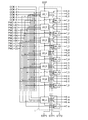
図2は、図1に示す表示装置が有する走査線駆動回路1の構成例を示す図である。図2に示す走査線駆動回路1は、第1の走査線駆動回路用クロック信号(GCK−1)を供給する配線〜第6の走査線駆動回路用クロック信号(GCK−6)を供給する配線と、第1のパルス幅制御信号A(PWC−A1)を供給する配線及び第2のパルス幅制御信号A(PWC−A2)を供給する配線と、第1のパルス幅制御信号B(PWC−B1)を供給する配線〜第6のパルス幅制御信号B(PWC−B6)を供給する配線と、第1のパルス幅制御信号C(PWC−C1)を供給する配線〜第3のパルス幅制御信号C(PWC−C3)を供給する配線と、走査線4_1、走査線5_1、及び走査線6_1を介して1行目に配設されたn個の画素10に電気的に接続された第1のパルス出力回路20_1〜走査線4_m、走査線5_m、及び走査線6_mを介してm行目に配設されたn個の画素10に電気的に接続された第mのパルス出力回路20_mと、反転走査線7_1を介して1行目に配設されたn個の画素10に電気的に接続された第1の反転パルス出力回路60_1〜反転走査線7_mを介してm行目に配設されたn個の画素10に電気的に接続された第mの反転パルス出力回路60_mとを有する。
図5(A)は、図2及び図4(A)に示すパルス出力回路の構成例を示す図である。図5(A)に示すパルス出力回路は、トランジスタ31〜トランジスタ42を有する。
上述したパルス出力回路の動作例について図5(B)を参照して説明する。なお、図5(B)には、第1のパルス出力回路20_1からシフトパルスが入力される際の第2のパルス出力回路20_2の各端子に入力される信号、及び各端子から出力される信号の電位、並びにノードA及びノードBの電位を示している。また、図中において、Gout4は、パルス出力回路の走査線4に対する出力信号を表し、Gout5は、パルス出力回路の走査線5に対する出力信号を表し、Gout6は、パルス出力回路の走査線6に対する出力信号を表し、SRoutは、当該パルス出力回路の、後段のパルス出力回路に対する出力信号を表している。
図6(A)は、図2及び図4(B)に示す反転パルス出力回路の構成例を示す図である。図6(A)に示す反転パルス出力回路は、トランジスタ71〜トランジスタ77を有する。
上述した反転パルス出力回路の動作例について図6(B)を参照して説明する。なお、図6(B)には、図6(B)に示す期間t1〜期間t4において第2の反転パルス出力回路20_2の各端子に入力される信号、及び出力される信号の電位、並びにノードCの電位を示している。また、図6(B)における期間t1〜期間t4は、図5(B)における期間t1〜t4と同じ期間である。また、図6(B)では、各端子に入力される信号を括弧書きで付記している。なお、図中において、GBoutは、反転パルス出力回路の反転走査線に対する出力信号を表している。
図7(A)は、図1に示す画素10の構成例を示す回路図である。図7(A)に示す画素10は、トランジスタ11〜16と、キャパシタ17、18と、一対の電極間に電流励起によって発光する有機物を備えた素子(以下、有機エレクトロルミネッセンス(EL)素子ともいう)19とを有する。
上述した画素の動作例について図7(A)、(B)を参照して説明する。具体的には、以下では、図5(B)及び図6(B)に示す期間t1〜期間t4に含まれる期間である期間ta〜期間thにおける画素の動作例について、図7(A)、(B)を参照して説明する。なお、図7(B)には、画素部において2行目に配設された走査線4_2、走査線5_2、及び走査線6_2、並びに反転走査線7_2の電位、並びにノードD〜ノードFの電位を示している。また、図7(B)では、各配線に入力される信号を括弧書きで付記している。
本明細書で開示される表示装置は、反転パルス出力回路の動作を複数種の信号によって制御する。これにより、当該反転パルス出力回路において生じる貫通電流を低減することが可能となる。また、当該複数種の信号として複数のパルス出力回路の動作に用いられる信号を適用する。すなわち、別途に信号を生成することなく、当該反転パルス出力回路を動作させることが可能である。
上述した表示装置は本発明の一態様であり、上述の表示装置と異なる構成を有する表示装置も本発明に含まれる。以下では、本発明の他の一態様について例示する。なお、本発明の他の一態様として例示する複数の内容を有する表示装置も本発明には含まれる。
上述の表示装置として、各画素に有機EL素子が設けられる表示装置(以下、EL表示装置ともいう)を例示したが、本発明の表示装置は、EL表示装置に限定されない。例えば、本発明の表示装置として、液晶の配向を制御することによって表示を行う表示装置(液晶表示装置)を適用することも可能である。
また、上述の走査線駆動回路の構成は、図2に示す構成に限定されない。例えば、図8に示す走査線駆動回路を上述の表示装置が有する走査線駆動回路として適用することも可能である。
また、上述の走査線駆動回路が有するパルス出力回路の構成は、図5(A)に示す構成に限定されない。例えば、図9〜11に示すパルス出力回路を上述の走査線駆動回路が有するパルス出力回路として適用することも可能である。
また、上述の走査線駆動回路が有する反転パルス出力回路の構成は、図6(A)に示す構成に限定されない。例えば、図12に示す反転パルス出力回路を上述の走査線駆動回路が有するパルス出力回路として適用することも可能である。
また、上述の表示装置が有する画素の構成は、図7(A)に示す構成に限定されない。例えば、図7(A)に示す画素はNチャネル型トランジスタのみによって構成されているが、本発明は当該構成に限定されない。すなわち、本発明の一態様の表示装置においては、Pチャネル型トランジスタのみを用いて画素を構成すること、又はNチャネル型トランジスタ及びPチャネル型トランジスタを組み合わせて画素を構成することも可能である。
以下では、本明細書で開示される液晶表示装置を搭載した電子機器の例について図13を参照して説明する。
2 信号線駆動回路
3 電流源
4〜6 走査線
7 反転走査線
8 信号線
9 電源線
10 画素
11〜16 トランジスタ
17、18 キャパシタ
19 有機EL素子
20 パルス出力回路
21〜30 端子
31〜42 トランジスタ
50〜55 トランジスタ
60 反転パルス出力回路
61〜65 端子
71〜77 トランジスタ
80 トランジスタ
2201 本体
2202 筐体
2203 表示部
2204 キーボード
2211 本体
2212 スタイラス
2213 表示部
2214 操作ボタン
2215 外部インターフェイス
2220 電子書籍
2221 筐体
2223 筐体
2225 表示部
2227 表示部
2231 電源
2233 操作キー
2235 スピーカー
2237 軸部
2240 筐体
2241 筐体
2242 表示パネル
2243 スピーカー
2244 マイクロフォン
2245 操作キー
2246 ポインティングデバイス
2247 カメラ用レンズ
2248 外部接続端子
2249 太陽電池セル
2250 外部メモリスロット
2261 本体
2263 接眼部
2264 操作スイッチ
2265 表示部(B)
2266 バッテリー
2267 表示部(A)
2270 テレビジョン装置
2271 筐体
2273 表示部
2275 スタンド
2277 表示部
2279 操作キー
2280 リモコン操作機
Claims (4)
- シフトパルスを出力する第1乃至第3のパルス出力回路と、反転パルス出力回路と、を有し、
反転パルス出力回路は、第1乃至第8のトランジスタを有し、
前記第1のトランジスタのソース又はドレインの一方は、前記第2のトランジスタのソース又はドレインの一方と電気的に接続され、
前記第1のトランジスタのソース又はドレインの一方は、前記第3のトランジスタのソース又はドレインの一方と電気的に接続され、
前記第1のトランジスタのソース又はドレインの一方は、前記第4のトランジスタのソース又はドレインの一方と電気的に接続され、
前記第5のトランジスタのソース又はドレインの一方は、前記第6のトランジスタのソース又はドレインの一方と電気的に接続され、
前記第5のトランジスタのソース又はドレインの一方は、前記第7のトランジスタのソース又はドレインの一方と電気的に接続され、
前記第5のトランジスタのソース又はドレインの一方は、走査線と電気的に接続され、
前記第8のトランジスタのソース又はドレインの一方は、前記第1のトランジスタのソース又はドレインの一方と電気的に接続され、
前記第8のトランジスタのソース又はドレインの他方は、前記第5のトランジスタのゲートと電気的に接続され、
前記第3のトランジスタのゲート及び前記第6のトランジスタのゲートは、前記第1のパルス出力回路の出力端子と電気的に接続され、
前記第4のトランジスタのゲート及び前記第7のトランジスタのゲートは、前記第2のパルス出力回路の出力端子と電気的に接続され、
前記第1のトランジスタのゲートは、クロック信号を供給する機能を有する配線と電気的に接続され、
前記第2のトランジスタのゲートは、前記第3のパルス出力回路の出力端子と電気的に接続されることを特徴とする半導体装置。 - 請求項1において、
前記第3のトランジスタ又は前記第4のトランジスタがオン状態になった後に、前記第2のトランジスタがオン状態になることを特徴とする半導体装置。 - 請求項1又は請求項2において、
前記第1乃至第3のパルス出力回路の一は、第11乃至第17のトランジスタを有し、
前記第11のトランジスタのソース又はドレインの一方は、前記第12のトランジスタのソース又はドレインの一方と電気的に接続され、
前記第13のトランジスタのソース又はドレインの一方は、前記第14のトランジスタのソース又はドレインの一方と電気的に接続され、
前記第15のトランジスタのソース又はドレインの一方は、前記第16のトランジスタのソース又はドレインの一方と電気的に接続され、
前記第15のトランジスタのソース又はドレインの一方は、前記第12のトランジスタのゲートと電気的に接続され、
前記第15のトランジスタのソース又はドレインの一方は、前記第14のトランジスタのゲートと電気的に接続され、
前記第17のトランジスタのソース又はドレインの一方は、前記第11のトランジスタのソース又はドレインの一方と電気的に接続され、
前記第17のトランジスタのソース又はドレインの他方は、前記第13のトランジスタのゲートと電気的に接続されることを特徴とする半導体装置。 - 請求項1乃至請求項3のいずれか一項に記載の半導体装置と、画素と、を有し、
前記画素は、第9及び第10のトランジスタと、有機EL素子と、を有し、
前記第9のトランジスタのソース又はドレインの一方は、電源線と電気的に接続され、
前記第9のトランジスタのソース又はドレインの他方は、前記第10のトランジスタのソース又はドレインの一方と電気的に接続され、
前記第10のトランジスタのソース又はドレインの他方は、前記有機EL素子と電気的に接続され、
前記第10トランジスタのゲートは、前記走査線と電気的に接続されることを特徴とする表示装置。
Priority Applications (1)
| Application Number | Priority Date | Filing Date | Title |
|---|---|---|---|
| JP2012255555A JP6074239B2 (ja) | 2011-11-30 | 2012-11-21 | 半導体装置及び表示装置 |
Applications Claiming Priority (3)
| Application Number | Priority Date | Filing Date | Title |
|---|---|---|---|
| JP2011261106 | 2011-11-30 | ||
| JP2011261106 | 2011-11-30 | ||
| JP2012255555A JP6074239B2 (ja) | 2011-11-30 | 2012-11-21 | 半導体装置及び表示装置 |
Publications (3)
| Publication Number | Publication Date |
|---|---|
| JP2013137528A JP2013137528A (ja) | 2013-07-11 |
| JP2013137528A5 JP2013137528A5 (ja) | 2016-01-07 |
| JP6074239B2 true JP6074239B2 (ja) | 2017-02-01 |
Family
ID=48466411
Family Applications (1)
| Application Number | Title | Priority Date | Filing Date |
|---|---|---|---|
| JP2012255555A Active JP6074239B2 (ja) | 2011-11-30 | 2012-11-21 | 半導体装置及び表示装置 |
Country Status (7)
| Country | Link |
|---|---|
| US (1) | US8847933B2 (ja) |
| JP (1) | JP6074239B2 (ja) |
| KR (1) | KR102082372B1 (ja) |
| CN (2) | CN103959364B (ja) |
| DE (1) | DE112012004996T5 (ja) |
| TW (2) | TWI570682B (ja) |
| WO (1) | WO2013080845A1 (ja) |
Families Citing this family (9)
| Publication number | Priority date | Publication date | Assignee | Title |
|---|---|---|---|---|
| KR102101167B1 (ko) | 2012-02-03 | 2020-04-16 | 가부시키가이샤 한도오따이 에네루기 켄큐쇼 | 반도체 장치 |
| US9362417B2 (en) | 2012-02-03 | 2016-06-07 | Semiconductor Energy Laboratory Co., Ltd. | Semiconductor device |
| US9041453B2 (en) | 2013-04-04 | 2015-05-26 | Semiconductor Energy Laboratory Co., Ltd. | Pulse generation circuit and semiconductor device |
| US9583063B2 (en) | 2013-09-12 | 2017-02-28 | Semiconductor Energy Laboratory Co., Ltd. | Display device |
| TWI627617B (zh) * | 2017-09-05 | 2018-06-21 | 友達光電股份有限公司 | 顯示裝置 |
| JP6781176B2 (ja) * | 2018-02-22 | 2020-11-04 | 株式会社Joled | 画素回路および表示装置 |
| JP7412360B2 (ja) | 2019-02-05 | 2024-01-12 | 株式会社半導体エネルギー研究所 | 表示装置および電子機器 |
| TWI756969B (zh) * | 2020-12-07 | 2022-03-01 | 友達光電股份有限公司 | 移位暫存器電路 |
| JP7697783B2 (ja) * | 2020-12-23 | 2025-06-24 | 武漢天馬微電子有限公司 | 表示装置 |
Family Cites Families (40)
| Publication number | Priority date | Publication date | Assignee | Title |
|---|---|---|---|---|
| JP3298974B2 (ja) | 1993-03-23 | 2002-07-08 | 電子科学株式会社 | 昇温脱離ガス分析装置 |
| US6859193B1 (en) | 1999-07-14 | 2005-02-22 | Sony Corporation | Current drive circuit and display device using the same, pixel circuit, and drive method |
| US7379039B2 (en) | 1999-07-14 | 2008-05-27 | Sony Corporation | Current drive circuit and display device using same pixel circuit, and drive method |
| TW582005B (en) | 2001-05-29 | 2004-04-01 | Semiconductor Energy Lab | Pulse output circuit, shift register, and display device |
| JP2003101394A (ja) | 2001-05-29 | 2003-04-04 | Semiconductor Energy Lab Co Ltd | パルス出力回路、シフトレジスタ、および表示装置 |
| US7365713B2 (en) | 2001-10-24 | 2008-04-29 | Semiconductor Energy Laboratory Co., Ltd. | Semiconductor device and driving method thereof |
| US7456810B2 (en) | 2001-10-26 | 2008-11-25 | Semiconductor Energy Laboratory Co., Ltd. | Light-emitting device and driving method thereof |
| JP3732477B2 (ja) * | 2001-10-26 | 2006-01-05 | 株式会社半導体エネルギー研究所 | 画素回路、発光装置および電子機器 |
| KR20050101182A (ko) | 2003-01-24 | 2005-10-20 | 코닌클리케 필립스 일렉트로닉스 엔.브이. | 액티브 매트릭스 디스플레이 디바이스 |
| GB0301659D0 (en) * | 2003-01-24 | 2003-02-26 | Koninkl Philips Electronics Nv | Electroluminescent display devices |
| JP4826870B2 (ja) * | 2003-12-02 | 2011-11-30 | ソニー株式会社 | 画素回路及びその駆動方法とアクティブマトリクス装置並びに表示装置 |
| DE602005010936D1 (de) | 2004-05-25 | 2008-12-24 | Samsung Sdi Co Ltd | Zeilenabtasttreiber für eine OLED-Anzeige |
| KR100578812B1 (ko) * | 2004-06-29 | 2006-05-11 | 삼성에스디아이 주식회사 | 발광 표시 장치 |
| KR100624317B1 (ko) * | 2004-12-24 | 2006-09-19 | 삼성에스디아이 주식회사 | 주사 구동부 및 이를 이용한 발광 표시장치와 그의 구동방법 |
| JP4993544B2 (ja) * | 2005-03-30 | 2012-08-08 | 三菱電機株式会社 | シフトレジスタ回路 |
| JP5160748B2 (ja) * | 2005-11-09 | 2013-03-13 | 三星ディスプレイ株式會社 | 発光表示装置 |
| JP4932415B2 (ja) * | 2006-09-29 | 2012-05-16 | 株式会社半導体エネルギー研究所 | 半導体装置 |
| JP5525685B2 (ja) | 2006-10-17 | 2014-06-18 | 株式会社半導体エネルギー研究所 | 半導体装置及び電子機器 |
| TWI427602B (zh) | 2006-10-17 | 2014-02-21 | Semiconductor Energy Lab | 脈衝輸出電路、移位暫存器及顯示裝置 |
| JP5090008B2 (ja) * | 2007-02-07 | 2012-12-05 | 三菱電機株式会社 | 半導体装置およびシフトレジスタ回路 |
| JP2008250093A (ja) | 2007-03-30 | 2008-10-16 | Sony Corp | 表示装置およびその駆動方法 |
| JP2008287134A (ja) * | 2007-05-21 | 2008-11-27 | Seiko Epson Corp | パルス出力回路、シフトレジスタ、走査線駆動回路、データ線駆動回路、電気光学装置及び電子機器 |
| US20080303769A1 (en) * | 2007-06-07 | 2008-12-11 | Mitsubishi Electric Corporation | Image display device and drive circuit |
| JP2009157148A (ja) * | 2007-12-27 | 2009-07-16 | Seiko Epson Corp | 発光装置の駆動方法および駆動方法、電子機器 |
| KR101448910B1 (ko) * | 2008-01-25 | 2014-10-14 | 삼성디스플레이 주식회사 | 게이트 구동회로 및 이를 갖는 표시장치 |
| JP2009188749A (ja) * | 2008-02-06 | 2009-08-20 | Sony Corp | インバータ回路、シフトレジスタ回路、否定論理和回路、否定論理積回路 |
| JP4844598B2 (ja) * | 2008-07-14 | 2011-12-28 | ソニー株式会社 | 走査駆動回路 |
| US8232947B2 (en) * | 2008-11-14 | 2012-07-31 | Semiconductor Energy Laboratory Co., Ltd. | Liquid crystal display device |
| US8330702B2 (en) * | 2009-02-12 | 2012-12-11 | Semiconductor Energy Laboratory Co., Ltd. | Pulse output circuit, display device, and electronic device |
| TW201039325A (en) * | 2009-04-23 | 2010-11-01 | Novatek Microelectronics Corp | Shift register apparatus |
| JP5436049B2 (ja) * | 2009-05-29 | 2014-03-05 | 三菱電機株式会社 | シフトレジスタ回路、シフトレジスタ回路の設計方法及び半導体装置 |
| US9715845B2 (en) * | 2009-09-16 | 2017-07-25 | Semiconductor Energy Laboratory Co., Ltd. | Semiconductor display device |
| US8068577B2 (en) * | 2009-09-23 | 2011-11-29 | Au Optronics Corporation | Pull-down control circuit and shift register of using same |
| CN107886916B (zh) * | 2009-12-18 | 2021-09-21 | 株式会社半导体能源研究所 | 液晶显示装置及其驱动方法 |
| JP5457826B2 (ja) * | 2009-12-28 | 2014-04-02 | 株式会社ジャパンディスプレイ | レベルシフト回路、信号駆動回路、表示装置および電子機器 |
| KR101752834B1 (ko) * | 2009-12-29 | 2017-07-03 | 삼성디스플레이 주식회사 | 게이트 구동회로 및 이를 포함하는 표시장치 |
| KR101324410B1 (ko) * | 2009-12-30 | 2013-11-01 | 엘지디스플레이 주식회사 | 쉬프트 레지스터와 이를 이용한 표시장치 |
| KR101097347B1 (ko) * | 2010-03-11 | 2011-12-21 | 삼성모바일디스플레이주식회사 | 게이트 구동 회로 및 이를 이용한 표시 장치 |
| JP5191522B2 (ja) * | 2010-10-29 | 2013-05-08 | 三菱電機株式会社 | シフトレジスタ回路 |
| WO2012157186A1 (en) | 2011-05-13 | 2012-11-22 | Semiconductor Energy Laboratory Co., Ltd. | Display device |
-
2012
- 2012-11-14 CN CN201280059326.0A patent/CN103959364B/zh not_active Expired - Fee Related
- 2012-11-14 DE DE112012004996.9T patent/DE112012004996T5/de active Pending
- 2012-11-14 CN CN201611102836.8A patent/CN106920512B/zh not_active Expired - Fee Related
- 2012-11-14 KR KR1020147017419A patent/KR102082372B1/ko active Active
- 2012-11-14 WO PCT/JP2012/080114 patent/WO2013080845A1/en not_active Ceased
- 2012-11-21 JP JP2012255555A patent/JP6074239B2/ja active Active
- 2012-11-28 US US13/687,744 patent/US8847933B2/en active Active
- 2012-11-28 TW TW101144494A patent/TWI570682B/zh not_active IP Right Cessation
- 2012-11-28 TW TW105138679A patent/TWI601108B/zh active
Also Published As
| Publication number | Publication date |
|---|---|
| US20130135278A1 (en) | 2013-05-30 |
| TWI570682B (zh) | 2017-02-11 |
| TW201717180A (zh) | 2017-05-16 |
| DE112012004996T5 (de) | 2014-09-11 |
| TWI601108B (zh) | 2017-10-01 |
| CN106920512B (zh) | 2019-12-03 |
| US8847933B2 (en) | 2014-09-30 |
| CN103959364B (zh) | 2017-01-18 |
| JP2013137528A (ja) | 2013-07-11 |
| CN103959364A (zh) | 2014-07-30 |
| CN106920512A (zh) | 2017-07-04 |
| KR102082372B1 (ko) | 2020-02-27 |
| KR20140108658A (ko) | 2014-09-12 |
| WO2013080845A1 (en) | 2013-06-06 |
| TW201322240A (zh) | 2013-06-01 |
Similar Documents
| Publication | Publication Date | Title |
|---|---|---|
| JP6074239B2 (ja) | 半導体装置及び表示装置 | |
| CN110972504B (zh) | 移位寄存器单元及驱动方法、栅极驱动电路、显示装置 | |
| US8564629B2 (en) | Liquid crystal display device and driving method thereof | |
| CN107331351B (zh) | 一种像素补偿电路、其驱动方法、显示面板及显示装置 | |
| JP5568510B2 (ja) | 半導体装置及びアクティブマトリクス型表示装置 | |
| JP2021013191A (ja) | 液晶表示装置 | |
| CN108281123A (zh) | 移位寄存器单元、栅极驱动电路、显示装置以及驱动方法 | |
| WO2021223579A1 (zh) | 像素驱动电路及驱动方法、移位寄存器电路、显示装置 | |
| CN109166542B (zh) | 移位寄存器单元及驱动方法、栅极驱动电路、显示装置 | |
| US11081031B2 (en) | Gate control unit, driving method thereof, gate driver on array and display apparatus | |
| US10748465B2 (en) | Gate drive circuit, display device and method for driving gate drive circuit | |
| JP2012150455A (ja) | 液晶表示装置の駆動方法 | |
| JP2008140490A (ja) | シフトレジスタ、走査線駆動回路、電気光学装置及び電子機器 | |
| KR102069321B1 (ko) | 스테이지 및 이를 이용한 유기전계발광 표시장치 | |
| JP2009049859A (ja) | 電気回路、電気回路の駆動方法、表示装置および電子機器。 | |
| CN220474323U (zh) | 显示装置 | |
| CN116825019A (zh) | 显示面板和显示装置 | |
| KR20150002250A (ko) | 게이트 구동부 및 이를 포함하는 평판표시장치 | |
| JP5061793B2 (ja) | 電気回路、電気回路の駆動方法、表示装置および電子機器。 | |
| CN118038788A (zh) | 一种显示面板和显示装置 | |
| CN121214858A (zh) | 显示面板的驱动电路和电子设备 |
Legal Events
| Date | Code | Title | Description |
|---|---|---|---|
| A521 | Request for written amendment filed |
Free format text: JAPANESE INTERMEDIATE CODE: A523 Effective date: 20151112 |
|
| A621 | Written request for application examination |
Free format text: JAPANESE INTERMEDIATE CODE: A621 Effective date: 20151112 |
|
| A977 | Report on retrieval |
Free format text: JAPANESE INTERMEDIATE CODE: A971007 Effective date: 20160729 |
|
| A131 | Notification of reasons for refusal |
Free format text: JAPANESE INTERMEDIATE CODE: A131 Effective date: 20160823 |
|
| A521 | Request for written amendment filed |
Free format text: JAPANESE INTERMEDIATE CODE: A523 Effective date: 20160916 |
|
| TRDD | Decision of grant or rejection written | ||
| A01 | Written decision to grant a patent or to grant a registration (utility model) |
Free format text: JAPANESE INTERMEDIATE CODE: A01 Effective date: 20161227 |
|
| A61 | First payment of annual fees (during grant procedure) |
Free format text: JAPANESE INTERMEDIATE CODE: A61 Effective date: 20170106 |
|
| R150 | Certificate of patent or registration of utility model |
Ref document number: 6074239 Country of ref document: JP Free format text: JAPANESE INTERMEDIATE CODE: R150 |
|
| R250 | Receipt of annual fees |
Free format text: JAPANESE INTERMEDIATE CODE: R250 |
|
| R250 | Receipt of annual fees |
Free format text: JAPANESE INTERMEDIATE CODE: R250 |
|
| R250 | Receipt of annual fees |
Free format text: JAPANESE INTERMEDIATE CODE: R250 |
|
| R250 | Receipt of annual fees |
Free format text: JAPANESE INTERMEDIATE CODE: R250 |
|
| R250 | Receipt of annual fees |
Free format text: JAPANESE INTERMEDIATE CODE: R250 |
|
| R250 | Receipt of annual fees |
Free format text: JAPANESE INTERMEDIATE CODE: R250 |
|
| R250 | Receipt of annual fees |
Free format text: JAPANESE INTERMEDIATE CODE: R250 |