JP5982758B2 - マイクロ波照射装置 - Google Patents
マイクロ波照射装置 Download PDFInfo
- Publication number
- JP5982758B2 JP5982758B2 JP2011192069A JP2011192069A JP5982758B2 JP 5982758 B2 JP5982758 B2 JP 5982758B2 JP 2011192069 A JP2011192069 A JP 2011192069A JP 2011192069 A JP2011192069 A JP 2011192069A JP 5982758 B2 JP5982758 B2 JP 5982758B2
- Authority
- JP
- Japan
- Prior art keywords
- gas
- wafer
- microwave
- processing
- microwave irradiation
- Prior art date
- Legal status (The legal status is an assumption and is not a legal conclusion. Google has not performed a legal analysis and makes no representation as to the accuracy of the status listed.)
- Active
Links
Images


Classifications
-
- H—ELECTRICITY
- H01—ELECTRIC ELEMENTS
- H01L—SEMICONDUCTOR DEVICES NOT COVERED BY CLASS H10
- H01L21/00—Processes or apparatus adapted for the manufacture or treatment of semiconductor or solid state devices or of parts thereof
- H01L21/67—Apparatus specially adapted for handling semiconductor or electric solid state devices during manufacture or treatment thereof; Apparatus specially adapted for handling wafers during manufacture or treatment of semiconductor or electric solid state devices or components ; Apparatus not specifically provided for elsewhere
- H01L21/67005—Apparatus not specifically provided for elsewhere
- H01L21/67011—Apparatus for manufacture or treatment
- H01L21/67017—Apparatus for fluid treatment
-
- H—ELECTRICITY
- H01—ELECTRIC ELEMENTS
- H01L—SEMICONDUCTOR DEVICES NOT COVERED BY CLASS H10
- H01L21/00—Processes or apparatus adapted for the manufacture or treatment of semiconductor or solid state devices or of parts thereof
- H01L21/02—Manufacture or treatment of semiconductor devices or of parts thereof
- H01L21/04—Manufacture or treatment of semiconductor devices or of parts thereof the devices having at least one potential-jump barrier or surface barrier, e.g. PN junction, depletion layer or carrier concentration layer
- H01L21/18—Manufacture or treatment of semiconductor devices or of parts thereof the devices having at least one potential-jump barrier or surface barrier, e.g. PN junction, depletion layer or carrier concentration layer the devices having semiconductor bodies comprising elements of Group IV of the Periodic System or AIIIBV compounds with or without impurities, e.g. doping materials
- H01L21/30—Treatment of semiconductor bodies using processes or apparatus not provided for in groups H01L21/20 - H01L21/26
- H01L21/324—Thermal treatment for modifying the properties of semiconductor bodies, e.g. annealing, sintering
-
- H—ELECTRICITY
- H01—ELECTRIC ELEMENTS
- H01L—SEMICONDUCTOR DEVICES NOT COVERED BY CLASS H10
- H01L21/00—Processes or apparatus adapted for the manufacture or treatment of semiconductor or solid state devices or of parts thereof
- H01L21/67—Apparatus specially adapted for handling semiconductor or electric solid state devices during manufacture or treatment thereof; Apparatus specially adapted for handling wafers during manufacture or treatment of semiconductor or electric solid state devices or components ; Apparatus not specifically provided for elsewhere
- H01L21/67005—Apparatus not specifically provided for elsewhere
- H01L21/67011—Apparatus for manufacture or treatment
- H01L21/67098—Apparatus for thermal treatment
- H01L21/67109—Apparatus for thermal treatment mainly by convection
-
- H—ELECTRICITY
- H01—ELECTRIC ELEMENTS
- H01L—SEMICONDUCTOR DEVICES NOT COVERED BY CLASS H10
- H01L21/00—Processes or apparatus adapted for the manufacture or treatment of semiconductor or solid state devices or of parts thereof
- H01L21/67—Apparatus specially adapted for handling semiconductor or electric solid state devices during manufacture or treatment thereof; Apparatus specially adapted for handling wafers during manufacture or treatment of semiconductor or electric solid state devices or components ; Apparatus not specifically provided for elsewhere
- H01L21/67005—Apparatus not specifically provided for elsewhere
- H01L21/67011—Apparatus for manufacture or treatment
- H01L21/67098—Apparatus for thermal treatment
- H01L21/67115—Apparatus for thermal treatment mainly by radiation
-
- H—ELECTRICITY
- H01—ELECTRIC ELEMENTS
- H01L—SEMICONDUCTOR DEVICES NOT COVERED BY CLASS H10
- H01L21/00—Processes or apparatus adapted for the manufacture or treatment of semiconductor or solid state devices or of parts thereof
- H01L21/67—Apparatus specially adapted for handling semiconductor or electric solid state devices during manufacture or treatment thereof; Apparatus specially adapted for handling wafers during manufacture or treatment of semiconductor or electric solid state devices or components ; Apparatus not specifically provided for elsewhere
- H01L21/67005—Apparatus not specifically provided for elsewhere
- H01L21/67242—Apparatus for monitoring, sorting or marking
- H01L21/67248—Temperature monitoring
-
- H—ELECTRICITY
- H05—ELECTRIC TECHNIQUES NOT OTHERWISE PROVIDED FOR
- H05B—ELECTRIC HEATING; ELECTRIC LIGHT SOURCES NOT OTHERWISE PROVIDED FOR; CIRCUIT ARRANGEMENTS FOR ELECTRIC LIGHT SOURCES, IN GENERAL
- H05B6/00—Heating by electric, magnetic or electromagnetic fields
- H05B6/64—Heating using microwaves
- H05B6/80—Apparatus for specific applications
- H05B6/806—Apparatus for specific applications for laboratory use
Description
本発明の関連技術によれば、被処理体に対してマイクロ波を照射しつつ放射温度計で被処理体の温度を測定し、この測定値に基づいて加熱手段とガス冷却手段とを制御することにより被処理体の温度を調整することができる。
本発明によれば、被処理体に対してマイクロ波を照射しつつ放射温度計で被処理体の温度を測定し、この測定値に基づいてガス冷却手段を制御することにより被処理体の温度を調整することができる。
本発明の他の関連技術によれば、被処理体に対してマイクロ波を照射しつつ放射温度計で被処理体の温度を測定し、この測定値に基づいて加熱手段を制御することにより被処理体の温度を調整することができる。
本発明の更に他の関連技術によれば、被処理体に対してマイクロ波を効率的に照射しつつ被処理体を効率的に冷却することができる。
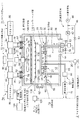
図示するように、このマイクロ波照射装置2は、アルミニウム、アルミニウム合金又はステンレス等により内部が断面円形に成形された筒体状の処理容器4を有している。この処理容器4内には、円板状になされた支持機構としての支持台6が、円筒状になされた支柱8により容器底部より起立されて設けられている。上記支持台6及び支柱8は、アルミニウム、アルミニウム合金又はステンレス等の金属により形成されている。
次に本発明のマイクロ波照射装置の第2実施例について説明する。半導体ウエハWの処理態様によっては、ウエハWの温度をそれ程高くする必要はなく、マイクロ波照射による加熱量で十分に目標とする温度滞域までウエハ温度を昇温できる場合がある。このような場合には、先の第1実施例で用いた加熱手段16を不要にすることができる。図4はこのような本発明に係るマイクロ波照射装置の第2実施例を示す構成図である。尚、図4において、先の図1乃至図3に示した部分と同一構成部分については同一参照符号を付してその説明を省略する。
次に本発明のマイクロ波照射装置の第3実施例について説明する。半導体ウエハWの処理態様によっては、プロセス温度が比較的高くウエハWの温度をガス冷却手段を用いて冷却する必要はなく、加熱手段の制御で十分に目標とする温度にウエハ温度を制御できる場合がある。このような場合には、先の第1実施例で用いたガス冷却手段104を不要にすることができる。図5はこのような本発明に係るマイクロ波照射装置の第3実施例を示す構成図である。尚、図5において、先の図1乃至図3に示した部分と同一構成部分については同一参照符号を付してその説明を省略する。
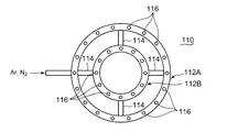
次に、ガス冷却手段(処理ガス導入手段)の変形例について説明する。先に説明した第1〜第3実施例においては、ガス冷却手段104或いは処理ガス導入手段106は、同心円状に配置された2本の分散管112A、112B(図3参照)を有していたが、これに限定されず、ノズルを用いてもよい。図6はガス冷却手段(処理ガス導入手段)の変形例を示す図である。尚、図6において先に説明した図と同一構成部分については同一参照符号を付して、その説明を省略する。
次に、本発明のマイクロ波照射装置の第4実施例について説明する。半導体ウエハの処理態様によっては、先の第2実施例と同様に、例えば下地膜等を熱的に保護する目的でウエハWのプロセス温度を低く抑えたい場合がある。このような場合には、第1実施例で用いた加熱手段16は不要になると共に、マイクロ波照射による加熱量でもウエハ温度はかなり上昇するので、プロセス中にはウエハを効率的に冷却する必要がある。
4 処理容器
6 支持台
10 支持ピン
12 チャック用密閉空間
14 真空チャック機構
16 加熱手段
18 発光素子ユニット
22 加熱電源
38 真空排気系
64 放射温度計
66 プローブライン
68 温度測定部
70 温度制御部
72 マイクロ波導入手段
74 マイクロ波ユニット
86 マイクロ波発生器
92 撹拌機
94 撹拌プロペラ
104 ガス冷却手段
106 処理ガス導入手段
110 シャワーヘッド部
132 リフトピン
134 リフタ機構
136 ガス冷却手段
138 真空チャック機構
140 リフト板
142 昇降ロッド
144 アクチュエータ
150 吸引孔
152 吸引通路
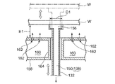
158 冷却ガス噴射箱
160 ガス拡散室
162 ガス噴射孔
164 ピン挿通管
W 半導体ウエハ(被処理体)
Claims (8)
- 被処理体に対してマイクロ波を照射して処理をするマイクロ波照射装置において、
前記被処理体を収容する処理容器と、
前記被処理体を支持する支持機構と、
前記処理容器内へ処理ガスを導入する処理ガス導入手段と、
前記処理容器内へマイクロ波を導入するマイクロ波導入手段と、
前記支持機構の上方に設置されたシャワーヘッド部を有して前記被処理体を冷却ガスにより冷却するガス冷却手段と、
前記被処理体の温度を測定する放射温度計と、
前記放射温度計の測定値に基づいて前記ガス冷却手段を制御することにより前記被処理体の温度を調整する温度制御部とを備え、
前記シャワーヘッド部から前記被処理体の被処理面に向けてシャワー状に冷却ガスを供給しながら前記マイクロ波を導入するように構成したことを特徴とするマイクロ波照射装置。 - 前記ガス冷却手段と前記ガス導入手段とは兼用されていることを特徴とする請求項1記載のマイクロ波照射装置。
- 前記処理容器内の天井部には、前記マイクロ波導入手段より導入されるマイクロ波を撹拌する撹拌機が設けられていることを特徴とする請求項1又は2記載のマイクロ波照射装置。
- 前記撹拌機と前記支持機構との間には、誘電体よりなる仕切板が設けられていることを特徴とする請求項3記載のマイクロ波照射装置。
- 前記仕切板の周辺部には、前記仕切板で仕切られた上下の空間を連通するための連通孔が形成されていることを特徴とする請求項4記載のマイクロ波照射装置。
- 前記被処理体は、前記支持機構上に複数の支持ピンを介して支持されていることを特徴とする請求項1乃至5のいずれか一項に記載のマイクロ波照射装置。
- 前記支持ピンは中空になされており、前記被処理体の裏面を吸着するチャック機構として形成されていることを特徴とする請求項6記載のマイクロ波照射装置。
- 前記支持機構の下部は、前記チャック機構の一部を形成するために真空引きされたチャック用密閉空間として形成されていると共に、前記チャック用密閉空間と前記支持ピンとは連通されていることを特徴とする請求項7記載のマイクロ波照射装置。
Priority Applications (5)
| Application Number | Priority Date | Filing Date | Title |
|---|---|---|---|
| JP2011192069A JP5982758B2 (ja) | 2011-02-23 | 2011-09-02 | マイクロ波照射装置 |
| US13/399,163 US9224623B2 (en) | 2011-02-23 | 2012-02-17 | Microwave irradiation apparatus |
| KR1020120017275A KR101332252B1 (ko) | 2011-02-23 | 2012-02-21 | 마이크로파 조사 장치 |
| TW101105730A TW201251515A (en) | 2011-02-23 | 2012-02-22 | Microwave irradiation apparatus |
| CN2012100445966A CN102651923A (zh) | 2011-02-23 | 2012-02-23 | 微波照射装置 |
Applications Claiming Priority (3)
| Application Number | Priority Date | Filing Date | Title |
|---|---|---|---|
| JP2011037396 | 2011-02-23 | ||
| JP2011037396 | 2011-02-23 | ||
| JP2011192069A JP5982758B2 (ja) | 2011-02-23 | 2011-09-02 | マイクロ波照射装置 |
Publications (3)
| Publication Number | Publication Date |
|---|---|
| JP2012191158A JP2012191158A (ja) | 2012-10-04 |
| JP2012191158A5 JP2012191158A5 (ja) | 2014-08-14 |
| JP5982758B2 true JP5982758B2 (ja) | 2016-08-31 |
Family
ID=46651903
Family Applications (1)
| Application Number | Title | Priority Date | Filing Date |
|---|---|---|---|
| JP2011192069A Active JP5982758B2 (ja) | 2011-02-23 | 2011-09-02 | マイクロ波照射装置 |
Country Status (5)
| Country | Link |
|---|---|
| US (1) | US9224623B2 (ja) |
| JP (1) | JP5982758B2 (ja) |
| KR (1) | KR101332252B1 (ja) |
| CN (1) | CN102651923A (ja) |
| TW (1) | TW201251515A (ja) |
Families Citing this family (26)
| Publication number | Priority date | Publication date | Assignee | Title |
|---|---|---|---|---|
| US9048270B2 (en) * | 2007-03-08 | 2015-06-02 | Joseph M. Wander | Apparatus and method for heating semiconductor wafers via microwaves |
| JP2014056806A (ja) * | 2012-02-27 | 2014-03-27 | Tokyo Electron Ltd | マイクロ波加熱処理装置および処理方法 |
| CN103389156A (zh) * | 2012-05-08 | 2013-11-13 | 全亿大科技(佛山)有限公司 | 发光二极管检测量具 |
| JP5738814B2 (ja) | 2012-09-12 | 2015-06-24 | 株式会社東芝 | マイクロ波アニール装置及び半導体装置の製造方法 |
| US9750091B2 (en) * | 2012-10-15 | 2017-08-29 | Applied Materials, Inc. | Apparatus and method for heat treatment of coatings on substrates |
| JP2014090058A (ja) * | 2012-10-30 | 2014-05-15 | Tokyo Electron Ltd | マイクロ波加熱処理装置および処理方法 |
| CN103792474A (zh) * | 2012-11-02 | 2014-05-14 | 全亿大科技(佛山)有限公司 | 发光二极管检测量具 |
| CN103008203B (zh) * | 2012-12-13 | 2015-07-15 | 京东方科技集团股份有限公司 | 一种膜固化装置 |
| US9989417B2 (en) * | 2013-09-12 | 2018-06-05 | Goji Limited | Temperature measurement arrangement |
| JP2015103726A (ja) * | 2013-11-27 | 2015-06-04 | 東京エレクトロン株式会社 | マイクロ波加熱処理装置及びマイクロ波加熱処理方法 |
| JP2015187955A (ja) * | 2014-03-27 | 2015-10-29 | 日本碍子株式会社 | マイクロ波照射方法 |
| JP6390153B2 (ja) * | 2014-04-30 | 2018-09-19 | 富士電機株式会社 | 熱処理装置 |
| KR101563495B1 (ko) * | 2014-07-31 | 2015-10-27 | 한국에너지기술연구원 | 광-전자적 측정 시에 샘플의 온도를 제어하는 장치 및 이를 이용한 태양전지 측정 장치 |
| JP6435135B2 (ja) * | 2014-08-26 | 2018-12-05 | 株式会社日立ハイテクノロジーズ | プラズマ処理装置 |
| US10403880B2 (en) * | 2015-09-11 | 2019-09-03 | Iftikhar Ahmad | Apparatus and method for processing battery electrodes |
| US11104502B2 (en) * | 2016-03-01 | 2021-08-31 | Jeffrey S. Melcher | Multi-function compact appliance and methods for a food or item in a container with a container storage technology |
| WO2017149663A1 (ja) * | 2016-03-01 | 2017-09-08 | 株式会社日立国際電気 | 基板処理装置、半導体装置の製造方法および記録媒体 |
| CN108660513A (zh) * | 2017-03-28 | 2018-10-16 | 上海新昇半导体科技有限公司 | 一种减少晶片缺陷的设备及方法 |
| KR102538177B1 (ko) | 2017-11-16 | 2023-05-31 | 삼성전자주식회사 | 상부 샤워 헤드 및 하부 샤워 헤드를 포함하는 증착 장치 |
| KR102404061B1 (ko) * | 2017-11-16 | 2022-05-31 | 삼성전자주식회사 | 상부 샤워 헤드 및 하부 샤워 헤드를 포함하는 증착 장치 |
| US10747968B2 (en) | 2017-11-22 | 2020-08-18 | Jeffrey S. Melcher | Wireless device and selective user control and management of a wireless device and data |
| JP7161854B2 (ja) * | 2018-03-05 | 2022-10-27 | 東京エレクトロン株式会社 | 検査装置 |
| JP7079317B2 (ja) * | 2018-03-23 | 2022-06-01 | 株式会社Kokusai Electric | 基板処理装置、半導体装置の製造方法及びプログラム |
| WO2019186655A1 (ja) * | 2018-03-26 | 2019-10-03 | 株式会社Kokusai Electric | 基板処理装置、半導体装置の製造方法およびプログラム |
| JP7338441B2 (ja) * | 2019-12-13 | 2023-09-05 | ウシオ電機株式会社 | 光加熱装置 |
| WO2023047922A1 (ja) * | 2021-09-24 | 2023-03-30 | 株式会社Kokusai Electric | 基板処理装置、半導体装置の製造方法およびプログラム |
Family Cites Families (31)
| Publication number | Priority date | Publication date | Assignee | Title |
|---|---|---|---|---|
| JPS6035992Y2 (ja) * | 1980-11-11 | 1985-10-25 | 株式会社東芝 | 高周波加熱装置 |
| JPH0752749B2 (ja) * | 1986-02-19 | 1995-06-05 | 富士通株式会社 | ウエハ−保持機構 |
| JPH07114188B2 (ja) * | 1988-02-25 | 1995-12-06 | 株式会社東芝 | 半導体基板の熱処理方法及びそれに用いる熱処理装置 |
| JPH0536641A (ja) * | 1991-08-01 | 1993-02-12 | Mitsubishi Electric Corp | 半導体製造装置 |
| JPH08139084A (ja) * | 1994-11-04 | 1996-05-31 | Kokusai Electric Co Ltd | 基板加熱装置 |
| JPH11243086A (ja) * | 1998-02-24 | 1999-09-07 | Sony Corp | 枚葉式cvd装置 |
| JP4053173B2 (ja) * | 1999-03-29 | 2008-02-27 | 東京エレクトロン株式会社 | マイクロ波プラズマ処理装置及び方法 |
| JP4236329B2 (ja) * | 1999-04-15 | 2009-03-11 | 日本碍子株式会社 | プラズマ処理装置 |
| JP3063761B2 (ja) * | 1999-05-31 | 2000-07-12 | 株式会社日立製作所 | プラズマ処理方法及び装置 |
| KR100338768B1 (ko) | 1999-10-25 | 2002-05-30 | 윤종용 | 산화막 제거방법 및 산화막 제거를 위한 반도체 제조 장치 |
| US7037797B1 (en) * | 2000-03-17 | 2006-05-02 | Mattson Technology, Inc. | Localized heating and cooling of substrates |
| TWI234417B (en) * | 2001-07-10 | 2005-06-11 | Tokyo Electron Ltd | Plasma procesor and plasma processing method |
| JP3912208B2 (ja) * | 2002-02-28 | 2007-05-09 | 東京エレクトロン株式会社 | 熱処理装置 |
| JP2004296625A (ja) * | 2003-03-26 | 2004-10-21 | Dainippon Screen Mfg Co Ltd | 基板処理装置、熱処理装置および熱処理方法 |
| JP3718688B2 (ja) * | 2003-06-17 | 2005-11-24 | 東京エレクトロン株式会社 | 加熱装置 |
| CN100492600C (zh) * | 2003-11-05 | 2009-05-27 | 大见忠弘 | 等离子体处理装置 |
| US8277569B2 (en) | 2004-07-01 | 2012-10-02 | Dainippon Screen Mfg. Co., Ltd. | Substrate treating apparatus and substrate treating method |
| US7436645B2 (en) | 2004-10-07 | 2008-10-14 | Applied Materials, Inc. | Method and apparatus for controlling temperature of a substrate |
| US7544251B2 (en) | 2004-10-07 | 2009-06-09 | Applied Materials, Inc. | Method and apparatus for controlling temperature of a substrate |
| JP2006173445A (ja) * | 2004-12-17 | 2006-06-29 | Hitachi High-Technologies Corp | 荷電粒子線装置 |
| CN101147244B (zh) * | 2005-07-28 | 2010-05-19 | 东京毅力科创株式会社 | 基板处理方法和基板处理装置 |
| JP5269602B2 (ja) | 2005-11-11 | 2013-08-21 | ディーエスジー テクノロジーズ | シリコンウエハを熱加工するための装置及び方法 |
| US7589028B1 (en) * | 2005-11-15 | 2009-09-15 | Novellus Systems, Inc. | Hydroxyl bond removal and film densification method for oxide films using microwave post treatment |
| KR101029691B1 (ko) | 2006-01-17 | 2011-04-15 | 다이닛뽕스크린 세이조오 가부시키가이샤 | 기판처리장치 및 기판처리방법 |
| JP2007258286A (ja) * | 2006-03-22 | 2007-10-04 | Tokyo Electron Ltd | 熱処理装置、熱処理方法及び記憶媒体 |
| JP5045000B2 (ja) | 2006-06-20 | 2012-10-10 | 東京エレクトロン株式会社 | 成膜装置、ガス供給装置、成膜方法及び記憶媒体 |
| WO2008081723A1 (ja) * | 2006-12-28 | 2008-07-10 | Tokyo Electron Limited | 絶縁膜の形成方法および半導体装置の製造方法 |
| JP5130761B2 (ja) * | 2007-03-23 | 2013-01-30 | 東京エレクトロン株式会社 | 載置台構造及び処理装置 |
| US7947570B2 (en) * | 2008-01-16 | 2011-05-24 | Semiconductor Energy Laboratory Co., Ltd. | Manufacturing method and manufacturing apparatus of semiconductor substrate |
| JP2010129790A (ja) | 2008-11-27 | 2010-06-10 | Tokyo Electron Ltd | 成膜方法 |
| JP4780202B2 (ja) * | 2009-02-05 | 2011-09-28 | パナソニック株式会社 | プラズマ処理装置 |
-
2011
- 2011-09-02 JP JP2011192069A patent/JP5982758B2/ja active Active
-
2012
- 2012-02-17 US US13/399,163 patent/US9224623B2/en active Active
- 2012-02-21 KR KR1020120017275A patent/KR101332252B1/ko active IP Right Grant
- 2012-02-22 TW TW101105730A patent/TW201251515A/zh unknown
- 2012-02-23 CN CN2012100445966A patent/CN102651923A/zh active Pending
Also Published As
| Publication number | Publication date |
|---|---|
| US20120211486A1 (en) | 2012-08-23 |
| KR20120096892A (ko) | 2012-08-31 |
| US9224623B2 (en) | 2015-12-29 |
| JP2012191158A (ja) | 2012-10-04 |
| CN102651923A (zh) | 2012-08-29 |
| KR101332252B1 (ko) | 2013-11-22 |
| TW201251515A (en) | 2012-12-16 |
Similar Documents
| Publication | Publication Date | Title |
|---|---|---|
| JP5982758B2 (ja) | マイクロ波照射装置 | |
| JP5077018B2 (ja) | 熱処理装置 | |
| JP5955394B2 (ja) | 基板処理装置、半導体装置の製造方法及びプログラム | |
| WO2005124840A1 (ja) | 熱処理装置 | |
| JP2009187990A (ja) | プラズマ処理装置 | |
| JP2011077065A (ja) | 熱処理装置 | |
| JP5657059B2 (ja) | マイクロ波加熱処理装置および処理方法 | |
| JP2002057209A (ja) | 枚葉式処理装置および枚葉式処理方法 | |
| TW202008467A (zh) | 熱處理裝置及熱處理方法 | |
| JP5560556B2 (ja) | 処理装置 | |
| JP4583618B2 (ja) | プラズマ処理装置 | |
| JP2009182177A (ja) | プラズマ処理システム | |
| JP2010034491A (ja) | アニール装置 | |
| JP2019212923A (ja) | 基板処理装置 | |
| TW201203373A (en) | Substrate processing apparatus and substrate processing method | |
| JP5155790B2 (ja) | 基板載置台およびそれを用いた基板処理装置 | |
| JP2016009796A (ja) | 基板加熱装置、基板支持装置、基板処理装置及び基板処理方法 | |
| TW201406211A (zh) | 加熱機構、成膜裝置及成膜方法 | |
| JP2010129861A (ja) | 熱処理装置 | |
| JP2011091389A (ja) | 基板処理装置及び半導体装置の製造方法 | |
| JP2008243844A (ja) | 載置台構造及び処理装置 | |
| WO2009157484A1 (ja) | アニール装置 | |
| JP4995579B2 (ja) | 基板処理装置及び半導体デバイスの製造方法 | |
| JP2011187786A (ja) | 熱処理装置 | |
| JP2010086985A (ja) | 基板処理装置 |
Legal Events
| Date | Code | Title | Description |
|---|---|---|---|
| A521 | Request for written amendment filed |
Free format text: JAPANESE INTERMEDIATE CODE: A523 Effective date: 20140630 |
|
| A621 | Written request for application examination |
Free format text: JAPANESE INTERMEDIATE CODE: A621 Effective date: 20140630 |
|
| A977 | Report on retrieval |
Free format text: JAPANESE INTERMEDIATE CODE: A971007 Effective date: 20150831 |
|
| A131 | Notification of reasons for refusal |
Free format text: JAPANESE INTERMEDIATE CODE: A131 Effective date: 20151006 |
|
| A521 | Request for written amendment filed |
Free format text: JAPANESE INTERMEDIATE CODE: A523 Effective date: 20151124 |
|
| TRDD | Decision of grant or rejection written | ||
| A01 | Written decision to grant a patent or to grant a registration (utility model) |
Free format text: JAPANESE INTERMEDIATE CODE: A01 Effective date: 20160705 |
|
| A61 | First payment of annual fees (during grant procedure) |
Free format text: JAPANESE INTERMEDIATE CODE: A61 Effective date: 20160718 |
|
| R150 | Certificate of patent or registration of utility model |
Ref document number: 5982758 Country of ref document: JP Free format text: JAPANESE INTERMEDIATE CODE: R150 |
|
| R250 | Receipt of annual fees |
Free format text: JAPANESE INTERMEDIATE CODE: R250 |
|
| R250 | Receipt of annual fees |
Free format text: JAPANESE INTERMEDIATE CODE: R250 |
|
| R250 | Receipt of annual fees |
Free format text: JAPANESE INTERMEDIATE CODE: R250 |
|
| R250 | Receipt of annual fees |
Free format text: JAPANESE INTERMEDIATE CODE: R250 |
|
| R250 | Receipt of annual fees |
Free format text: JAPANESE INTERMEDIATE CODE: R250 |