JP5951191B2 - Method for manufacturing semiconductor device - Google Patents
Method for manufacturing semiconductor device Download PDFInfo
- Publication number
- JP5951191B2 JP5951191B2 JP2011110963A JP2011110963A JP5951191B2 JP 5951191 B2 JP5951191 B2 JP 5951191B2 JP 2011110963 A JP2011110963 A JP 2011110963A JP 2011110963 A JP2011110963 A JP 2011110963A JP 5951191 B2 JP5951191 B2 JP 5951191B2
- Authority
- JP
- Japan
- Prior art keywords
- layer
- oxide semiconductor
- insulating layer
- film
- conductive
- Prior art date
- Legal status (The legal status is an assumption and is not a legal conclusion. Google has not performed a legal analysis and makes no representation as to the accuracy of the status listed.)
- Active
Links
- 239000004065 semiconductor Substances 0.000 title claims description 321
- 238000000034 method Methods 0.000 title claims description 88
- 238000004519 manufacturing process Methods 0.000 title claims description 32
- 229910052760 oxygen Inorganic materials 0.000 claims description 38
- 239000001301 oxygen Substances 0.000 claims description 38
- QVGXLLKOCUKJST-UHFFFAOYSA-N atomic oxygen Chemical compound [O] QVGXLLKOCUKJST-UHFFFAOYSA-N 0.000 claims description 37
- 150000001768 cations Chemical class 0.000 claims description 36
- 229910052736 halogen Inorganic materials 0.000 claims description 14
- 150000002367 halogens Chemical class 0.000 claims description 14
- 239000012212 insulator Substances 0.000 claims description 12
- 239000010410 layer Substances 0.000 description 459
- 239000010408 film Substances 0.000 description 200
- 239000000758 substrate Substances 0.000 description 115
- 238000010438 heat treatment Methods 0.000 description 99
- 239000000463 material Substances 0.000 description 53
- 239000010409 thin film Substances 0.000 description 42
- 239000012298 atmosphere Substances 0.000 description 36
- 239000004973 liquid crystal related substance Substances 0.000 description 34
- 238000009832 plasma treatment Methods 0.000 description 34
- 229910007541 Zn O Inorganic materials 0.000 description 31
- 238000005530 etching Methods 0.000 description 28
- XLOMVQKBTHCTTD-UHFFFAOYSA-N Zinc monoxide Chemical compound [Zn]=O XLOMVQKBTHCTTD-UHFFFAOYSA-N 0.000 description 27
- 239000001257 hydrogen Substances 0.000 description 25
- 229910052739 hydrogen Inorganic materials 0.000 description 25
- IJGRMHOSHXDMSA-UHFFFAOYSA-N Atomic nitrogen Chemical compound N#N IJGRMHOSHXDMSA-UHFFFAOYSA-N 0.000 description 24
- 230000006870 function Effects 0.000 description 24
- UFHFLCQGNIYNRP-UHFFFAOYSA-N Hydrogen Chemical compound [H][H] UFHFLCQGNIYNRP-UHFFFAOYSA-N 0.000 description 22
- 238000004544 sputter deposition Methods 0.000 description 22
- 125000004429 atom Chemical group 0.000 description 21
- 229910052782 aluminium Inorganic materials 0.000 description 19
- VYPSYNLAJGMNEJ-UHFFFAOYSA-N silicon dioxide Inorganic materials O=[Si]=O VYPSYNLAJGMNEJ-UHFFFAOYSA-N 0.000 description 18
- XAGFODPZIPBFFR-UHFFFAOYSA-N aluminium Chemical compound [Al] XAGFODPZIPBFFR-UHFFFAOYSA-N 0.000 description 17
- 238000005268 plasma chemical vapour deposition Methods 0.000 description 17
- 239000002585 base Substances 0.000 description 16
- 238000005401 electroluminescence Methods 0.000 description 16
- 229910052814 silicon oxide Inorganic materials 0.000 description 16
- 239000004020 conductor Substances 0.000 description 15
- 239000011521 glass Substances 0.000 description 15
- 239000011787 zinc oxide Substances 0.000 description 15
- -1 and the like Substances 0.000 description 14
- 238000001312 dry etching Methods 0.000 description 14
- 239000007789 gas Substances 0.000 description 14
- 229910052751 metal Inorganic materials 0.000 description 14
- 229910052581 Si3N4 Inorganic materials 0.000 description 13
- 239000000460 chlorine Substances 0.000 description 13
- 239000002184 metal Substances 0.000 description 13
- HQVNEWCFYHHQES-UHFFFAOYSA-N silicon nitride Chemical compound N12[Si]34N5[Si]62N3[Si]51N64 HQVNEWCFYHHQES-UHFFFAOYSA-N 0.000 description 13
- 230000015572 biosynthetic process Effects 0.000 description 12
- 238000004891 communication Methods 0.000 description 12
- 230000007547 defect Effects 0.000 description 12
- 229910052757 nitrogen Inorganic materials 0.000 description 12
- 238000012545 processing Methods 0.000 description 12
- 239000010936 titanium Substances 0.000 description 12
- 238000001039 wet etching Methods 0.000 description 12
- 238000009616 inductively coupled plasma Methods 0.000 description 11
- 239000000203 mixture Substances 0.000 description 11
- 239000010949 copper Substances 0.000 description 10
- 229910052733 gallium Inorganic materials 0.000 description 10
- 150000002500 ions Chemical class 0.000 description 10
- 229920005989 resin Polymers 0.000 description 10
- 239000011347 resin Substances 0.000 description 10
- 239000000565 sealant Substances 0.000 description 10
- 239000011701 zinc Substances 0.000 description 10
- 239000002356 single layer Substances 0.000 description 9
- XKRFYHLGVUSROY-UHFFFAOYSA-N Argon Chemical compound [Ar] XKRFYHLGVUSROY-UHFFFAOYSA-N 0.000 description 8
- RYGMFSIKBFXOCR-UHFFFAOYSA-N Copper Chemical compound [Cu] RYGMFSIKBFXOCR-UHFFFAOYSA-N 0.000 description 8
- XUIMIQQOPSSXEZ-UHFFFAOYSA-N Silicon Chemical compound [Si] XUIMIQQOPSSXEZ-UHFFFAOYSA-N 0.000 description 8
- RTAQQCXQSZGOHL-UHFFFAOYSA-N Titanium Chemical compound [Ti] RTAQQCXQSZGOHL-UHFFFAOYSA-N 0.000 description 8
- 229910052802 copper Inorganic materials 0.000 description 8
- 230000000694 effects Effects 0.000 description 8
- 229910003437 indium oxide Inorganic materials 0.000 description 8
- PJXISJQVUVHSOJ-UHFFFAOYSA-N indium(iii) oxide Chemical compound [O-2].[O-2].[O-2].[In+3].[In+3] PJXISJQVUVHSOJ-UHFFFAOYSA-N 0.000 description 8
- 239000012299 nitrogen atmosphere Substances 0.000 description 8
- 229910052710 silicon Inorganic materials 0.000 description 8
- 239000010703 silicon Substances 0.000 description 8
- 229910052719 titanium Inorganic materials 0.000 description 8
- 230000008859 change Effects 0.000 description 7
- 229910052738 indium Inorganic materials 0.000 description 7
- AMGQUBHHOARCQH-UHFFFAOYSA-N indium;oxotin Chemical compound [In].[Sn]=O AMGQUBHHOARCQH-UHFFFAOYSA-N 0.000 description 7
- 239000011159 matrix material Substances 0.000 description 7
- 229910052750 molybdenum Inorganic materials 0.000 description 7
- 239000011733 molybdenum Substances 0.000 description 7
- 230000008569 process Effects 0.000 description 7
- QTBSBXVTEAMEQO-UHFFFAOYSA-N Acetic acid Chemical compound CC(O)=O QTBSBXVTEAMEQO-UHFFFAOYSA-N 0.000 description 6
- ZOKXTWBITQBERF-UHFFFAOYSA-N Molybdenum Chemical compound [Mo] ZOKXTWBITQBERF-UHFFFAOYSA-N 0.000 description 6
- 125000001309 chloro group Chemical group Cl* 0.000 description 6
- 238000011161 development Methods 0.000 description 6
- 239000011229 interlayer Substances 0.000 description 6
- 229910044991 metal oxide Inorganic materials 0.000 description 6
- 150000004706 metal oxides Chemical class 0.000 description 6
- 229910052725 zinc Inorganic materials 0.000 description 6
- PXHVJJICTQNCMI-UHFFFAOYSA-N Nickel Chemical compound [Ni] PXHVJJICTQNCMI-UHFFFAOYSA-N 0.000 description 5
- 239000000956 alloy Substances 0.000 description 5
- 229910045601 alloy Inorganic materials 0.000 description 5
- 239000003990 capacitor Substances 0.000 description 5
- 239000000969 carrier Substances 0.000 description 5
- 229910052801 chlorine Inorganic materials 0.000 description 5
- 239000000945 filler Substances 0.000 description 5
- 239000012535 impurity Substances 0.000 description 5
- 238000003780 insertion Methods 0.000 description 5
- 230000037431 insertion Effects 0.000 description 5
- QGLKJKCYBOYXKC-UHFFFAOYSA-N nonaoxidotritungsten Chemical compound O=[W]1(=O)O[W](=O)(=O)O[W](=O)(=O)O1 QGLKJKCYBOYXKC-UHFFFAOYSA-N 0.000 description 5
- TWNQGVIAIRXVLR-UHFFFAOYSA-N oxo(oxoalumanyloxy)alumane Chemical compound O=[Al]O[Al]=O TWNQGVIAIRXVLR-UHFFFAOYSA-N 0.000 description 5
- BPUBBGLMJRNUCC-UHFFFAOYSA-N oxygen(2-);tantalum(5+) Chemical compound [O-2].[O-2].[O-2].[O-2].[O-2].[Ta+5].[Ta+5] BPUBBGLMJRNUCC-UHFFFAOYSA-N 0.000 description 5
- 229920003023 plastic Polymers 0.000 description 5
- 239000004033 plastic Substances 0.000 description 5
- 125000006850 spacer group Chemical group 0.000 description 5
- 239000012798 spherical particle Substances 0.000 description 5
- 229910001936 tantalum oxide Inorganic materials 0.000 description 5
- 229910001930 tungsten oxide Inorganic materials 0.000 description 5
- YVTHLONGBIQYBO-UHFFFAOYSA-N zinc indium(3+) oxygen(2-) Chemical compound [O--].[Zn++].[In+3] YVTHLONGBIQYBO-UHFFFAOYSA-N 0.000 description 5
- ZAMOUSCENKQFHK-UHFFFAOYSA-N Chlorine atom Chemical compound [Cl] ZAMOUSCENKQFHK-UHFFFAOYSA-N 0.000 description 4
- GYHNNYVSQQEPJS-UHFFFAOYSA-N Gallium Chemical compound [Ga] GYHNNYVSQQEPJS-UHFFFAOYSA-N 0.000 description 4
- NBIIXXVUZAFLBC-UHFFFAOYSA-N Phosphoric acid Chemical compound OP(O)(O)=O NBIIXXVUZAFLBC-UHFFFAOYSA-N 0.000 description 4
- GWEVSGVZZGPLCZ-UHFFFAOYSA-N Titan oxide Chemical compound O=[Ti]=O GWEVSGVZZGPLCZ-UHFFFAOYSA-N 0.000 description 4
- 229910052786 argon Inorganic materials 0.000 description 4
- 239000011651 chromium Substances 0.000 description 4
- 229920001940 conductive polymer Polymers 0.000 description 4
- 239000013078 crystal Substances 0.000 description 4
- OSVXSBDYLRYLIG-UHFFFAOYSA-N dioxidochlorine(.) Chemical compound O=Cl=O OSVXSBDYLRYLIG-UHFFFAOYSA-N 0.000 description 4
- 230000005284 excitation Effects 0.000 description 4
- 238000000605 extraction Methods 0.000 description 4
- 239000010419 fine particle Substances 0.000 description 4
- 239000011810 insulating material Substances 0.000 description 4
- 229910052749 magnesium Inorganic materials 0.000 description 4
- OGIDPMRJRNCKJF-UHFFFAOYSA-N titanium oxide Inorganic materials [Ti]=O OGIDPMRJRNCKJF-UHFFFAOYSA-N 0.000 description 4
- WFKWXMTUELFFGS-UHFFFAOYSA-N tungsten Chemical compound [W] WFKWXMTUELFFGS-UHFFFAOYSA-N 0.000 description 4
- 229910052721 tungsten Inorganic materials 0.000 description 4
- 239000010937 tungsten Substances 0.000 description 4
- BSYNRYMUTXBXSQ-UHFFFAOYSA-N Aspirin Chemical compound CC(=O)OC1=CC=CC=C1C(O)=O BSYNRYMUTXBXSQ-UHFFFAOYSA-N 0.000 description 3
- MYMOFIZGZYHOMD-UHFFFAOYSA-N Dioxygen Chemical compound O=O MYMOFIZGZYHOMD-UHFFFAOYSA-N 0.000 description 3
- XEEYBQQBJWHFJM-UHFFFAOYSA-N Iron Chemical compound [Fe] XEEYBQQBJWHFJM-UHFFFAOYSA-N 0.000 description 3
- 229910019092 Mg-O Inorganic materials 0.000 description 3
- 229910019395 Mg—O Inorganic materials 0.000 description 3
- 229910052779 Neodymium Inorganic materials 0.000 description 3
- 230000002411 adverse Effects 0.000 description 3
- 229910052791 calcium Inorganic materials 0.000 description 3
- 239000000919 ceramic Substances 0.000 description 3
- 239000000470 constituent Substances 0.000 description 3
- 238000003795 desorption Methods 0.000 description 3
- 238000009792 diffusion process Methods 0.000 description 3
- 229910001882 dioxygen Inorganic materials 0.000 description 3
- KPUWHANPEXNPJT-UHFFFAOYSA-N disiloxane Chemical class [SiH3]O[SiH3] KPUWHANPEXNPJT-UHFFFAOYSA-N 0.000 description 3
- 230000005684 electric field Effects 0.000 description 3
- 230000002349 favourable effect Effects 0.000 description 3
- 150000002431 hydrogen Chemical class 0.000 description 3
- APFVFJFRJDLVQX-UHFFFAOYSA-N indium atom Chemical compound [In] APFVFJFRJDLVQX-UHFFFAOYSA-N 0.000 description 3
- 239000007788 liquid Substances 0.000 description 3
- 230000007774 longterm Effects 0.000 description 3
- 230000007246 mechanism Effects 0.000 description 3
- QEFYFXOXNSNQGX-UHFFFAOYSA-N neodymium atom Chemical compound [Nd] QEFYFXOXNSNQGX-UHFFFAOYSA-N 0.000 description 3
- 229910052759 nickel Inorganic materials 0.000 description 3
- 239000002245 particle Substances 0.000 description 3
- 229920006267 polyester film Polymers 0.000 description 3
- 229920002620 polyvinyl fluoride Polymers 0.000 description 3
- 230000001681 protective effect Effects 0.000 description 3
- 238000007650 screen-printing Methods 0.000 description 3
- 239000007787 solid Substances 0.000 description 3
- 238000004528 spin coating Methods 0.000 description 3
- 239000010935 stainless steel Substances 0.000 description 3
- 229910001220 stainless steel Inorganic materials 0.000 description 3
- 238000001771 vacuum deposition Methods 0.000 description 3
- UWCWUCKPEYNDNV-LBPRGKRZSA-N 2,6-dimethyl-n-[[(2s)-pyrrolidin-2-yl]methyl]aniline Chemical compound CC1=CC=CC(C)=C1NC[C@H]1NCCC1 UWCWUCKPEYNDNV-LBPRGKRZSA-N 0.000 description 2
- 239000004925 Acrylic resin Substances 0.000 description 2
- 229920000178 Acrylic resin Polymers 0.000 description 2
- PAYRUJLWNCNPSJ-UHFFFAOYSA-N Aniline Chemical compound NC1=CC=CC=C1 PAYRUJLWNCNPSJ-UHFFFAOYSA-N 0.000 description 2
- CURLTUGMZLYLDI-UHFFFAOYSA-N Carbon dioxide Chemical compound O=C=O CURLTUGMZLYLDI-UHFFFAOYSA-N 0.000 description 2
- 239000004155 Chlorine dioxide Substances 0.000 description 2
- VYZAMTAEIAYCRO-UHFFFAOYSA-N Chromium Chemical compound [Cr] VYZAMTAEIAYCRO-UHFFFAOYSA-N 0.000 description 2
- GRYLNZFGIOXLOG-UHFFFAOYSA-N Nitric acid Chemical compound O[N+]([O-])=O GRYLNZFGIOXLOG-UHFFFAOYSA-N 0.000 description 2
- 239000004642 Polyimide Substances 0.000 description 2
- KAESVJOAVNADME-UHFFFAOYSA-N Pyrrole Chemical compound C=1C=CNC=1 KAESVJOAVNADME-UHFFFAOYSA-N 0.000 description 2
- YTPLMLYBLZKORZ-UHFFFAOYSA-N Thiophene Chemical compound C=1C=CSC=1 YTPLMLYBLZKORZ-UHFFFAOYSA-N 0.000 description 2
- HCHKCACWOHOZIP-UHFFFAOYSA-N Zinc Chemical compound [Zn] HCHKCACWOHOZIP-UHFFFAOYSA-N 0.000 description 2
- 230000001133 acceleration Effects 0.000 description 2
- NIXOWILDQLNWCW-UHFFFAOYSA-N acrylic acid group Chemical group C(C=C)(=O)O NIXOWILDQLNWCW-UHFFFAOYSA-N 0.000 description 2
- 230000001154 acute effect Effects 0.000 description 2
- 239000003513 alkali Substances 0.000 description 2
- 229910052783 alkali metal Inorganic materials 0.000 description 2
- 150000001340 alkali metals Chemical class 0.000 description 2
- 229910052784 alkaline earth metal Inorganic materials 0.000 description 2
- 150000001342 alkaline earth metals Chemical class 0.000 description 2
- 229910000147 aluminium phosphate Inorganic materials 0.000 description 2
- 239000005407 aluminoborosilicate glass Substances 0.000 description 2
- 239000005354 aluminosilicate glass Substances 0.000 description 2
- 229910052788 barium Inorganic materials 0.000 description 2
- DSAJWYNOEDNPEQ-UHFFFAOYSA-N barium atom Chemical compound [Ba] DSAJWYNOEDNPEQ-UHFFFAOYSA-N 0.000 description 2
- 230000008901 benefit Effects 0.000 description 2
- 230000000903 blocking effect Effects 0.000 description 2
- 239000005388 borosilicate glass Substances 0.000 description 2
- DQXBYHZEEUGOBF-UHFFFAOYSA-N but-3-enoic acid;ethene Chemical compound C=C.OC(=O)CC=C DQXBYHZEEUGOBF-UHFFFAOYSA-N 0.000 description 2
- 230000001413 cellular effect Effects 0.000 description 2
- 235000019398 chlorine dioxide Nutrition 0.000 description 2
- 229910052804 chromium Inorganic materials 0.000 description 2
- 150000001875 compounds Chemical class 0.000 description 2
- 238000001816 cooling Methods 0.000 description 2
- 230000007797 corrosion Effects 0.000 description 2
- 238000005260 corrosion Methods 0.000 description 2
- 238000000151 deposition Methods 0.000 description 2
- 230000008021 deposition Effects 0.000 description 2
- 238000009826 distribution Methods 0.000 description 2
- 238000001678 elastic recoil detection analysis Methods 0.000 description 2
- 239000003822 epoxy resin Substances 0.000 description 2
- 239000005038 ethylene vinyl acetate Substances 0.000 description 2
- 230000001747 exhibiting effect Effects 0.000 description 2
- 239000005262 ferroelectric liquid crystals (FLCs) Substances 0.000 description 2
- 239000011152 fibreglass Substances 0.000 description 2
- 230000005669 field effect Effects 0.000 description 2
- 229910052731 fluorine Inorganic materials 0.000 description 2
- 239000011737 fluorine Substances 0.000 description 2
- 125000001153 fluoro group Chemical group F* 0.000 description 2
- 229910052735 hafnium Inorganic materials 0.000 description 2
- 238000002347 injection Methods 0.000 description 2
- 239000007924 injection Substances 0.000 description 2
- 229910052742 iron Inorganic materials 0.000 description 2
- 229910052747 lanthanoid Inorganic materials 0.000 description 2
- 150000002602 lanthanoids Chemical class 0.000 description 2
- 239000011572 manganese Substances 0.000 description 2
- 239000011259 mixed solution Substances 0.000 description 2
- 229910017604 nitric acid Inorganic materials 0.000 description 2
- 150000004767 nitrides Chemical class 0.000 description 2
- 230000003287 optical effect Effects 0.000 description 2
- 150000002894 organic compounds Chemical class 0.000 description 2
- 125000000962 organic group Chemical group 0.000 description 2
- 239000011368 organic material Substances 0.000 description 2
- 230000003647 oxidation Effects 0.000 description 2
- 238000007254 oxidation reaction Methods 0.000 description 2
- 238000005192 partition Methods 0.000 description 2
- 238000001020 plasma etching Methods 0.000 description 2
- 229920001200 poly(ethylene-vinyl acetate) Polymers 0.000 description 2
- 229920002037 poly(vinyl butyral) polymer Polymers 0.000 description 2
- 229920000647 polyepoxide Polymers 0.000 description 2
- 229920001721 polyimide Polymers 0.000 description 2
- 229920000915 polyvinyl chloride Polymers 0.000 description 2
- 239000004800 polyvinyl chloride Substances 0.000 description 2
- 239000010453 quartz Substances 0.000 description 2
- 238000005001 rutherford backscattering spectroscopy Methods 0.000 description 2
- 229910052594 sapphire Inorganic materials 0.000 description 2
- 239000010980 sapphire Substances 0.000 description 2
- 229910052706 scandium Inorganic materials 0.000 description 2
- SIXSYDAISGFNSX-UHFFFAOYSA-N scandium atom Chemical compound [Sc] SIXSYDAISGFNSX-UHFFFAOYSA-N 0.000 description 2
- 229910052708 sodium Inorganic materials 0.000 description 2
- 239000000243 solution Substances 0.000 description 2
- 238000003860 storage Methods 0.000 description 2
- 238000003786 synthesis reaction Methods 0.000 description 2
- 229910052715 tantalum Inorganic materials 0.000 description 2
- GUVRBAGPIYLISA-UHFFFAOYSA-N tantalum atom Chemical compound [Ta] GUVRBAGPIYLISA-UHFFFAOYSA-N 0.000 description 2
- JBQYATWDVHIOAR-UHFFFAOYSA-N tellanylidenegermanium Chemical compound [Te]=[Ge] JBQYATWDVHIOAR-UHFFFAOYSA-N 0.000 description 2
- 229910052718 tin Inorganic materials 0.000 description 2
- 230000007704 transition Effects 0.000 description 2
- 229910052723 transition metal Inorganic materials 0.000 description 2
- 238000002834 transmittance Methods 0.000 description 2
- 210000003462 vein Anatomy 0.000 description 2
- 229910017073 AlLi Inorganic materials 0.000 description 1
- OKTJSMMVPCPJKN-UHFFFAOYSA-N Carbon Chemical compound [C] OKTJSMMVPCPJKN-UHFFFAOYSA-N 0.000 description 1
- YCKRFDGAMUMZLT-UHFFFAOYSA-N Fluorine atom Chemical compound [F] YCKRFDGAMUMZLT-UHFFFAOYSA-N 0.000 description 1
- 229910005191 Ga 2 O 3 Inorganic materials 0.000 description 1
- 206010052128 Glare Diseases 0.000 description 1
- 206010021143 Hypoxia Diseases 0.000 description 1
- PWHULOQIROXLJO-UHFFFAOYSA-N Manganese Chemical compound [Mn] PWHULOQIROXLJO-UHFFFAOYSA-N 0.000 description 1
- OAICVXFJPJFONN-UHFFFAOYSA-N Phosphorus Chemical compound [P] OAICVXFJPJFONN-UHFFFAOYSA-N 0.000 description 1
- 239000004952 Polyamide Substances 0.000 description 1
- 229910004298 SiO 2 Inorganic materials 0.000 description 1
- 229910002808 Si–O–Si Inorganic materials 0.000 description 1
- 229910020833 Sn-Al-Zn Inorganic materials 0.000 description 1
- 229910020923 Sn-O Inorganic materials 0.000 description 1
- 229910006404 SnO 2 Inorganic materials 0.000 description 1
- GDFCWFBWQUEQIJ-UHFFFAOYSA-N [B].[P] Chemical compound [B].[P] GDFCWFBWQUEQIJ-UHFFFAOYSA-N 0.000 description 1
- 125000000217 alkyl group Chemical group 0.000 description 1
- 125000003118 aryl group Chemical group 0.000 description 1
- UMIVXZPTRXBADB-UHFFFAOYSA-N benzocyclobutene Chemical compound C1=CC=C2CCC2=C1 UMIVXZPTRXBADB-UHFFFAOYSA-N 0.000 description 1
- 230000002457 bidirectional effect Effects 0.000 description 1
- 239000011230 binding agent Substances 0.000 description 1
- 239000005380 borophosphosilicate glass Substances 0.000 description 1
- 229910052799 carbon Inorganic materials 0.000 description 1
- 239000001569 carbon dioxide Substances 0.000 description 1
- 229910002092 carbon dioxide Inorganic materials 0.000 description 1
- 238000005229 chemical vapour deposition Methods 0.000 description 1
- 230000003098 cholesteric effect Effects 0.000 description 1
- 229910017052 cobalt Inorganic materials 0.000 description 1
- 239000010941 cobalt Substances 0.000 description 1
- GUTLYIVDDKVIGB-UHFFFAOYSA-N cobalt atom Chemical compound [Co] GUTLYIVDDKVIGB-UHFFFAOYSA-N 0.000 description 1
- 238000004040 coloring Methods 0.000 description 1
- 229920001577 copolymer Polymers 0.000 description 1
- 238000007872 degassing Methods 0.000 description 1
- 238000013461 design Methods 0.000 description 1
- 238000001514 detection method Methods 0.000 description 1
- 239000010432 diamond Substances 0.000 description 1
- 229910003460 diamond Inorganic materials 0.000 description 1
- 238000003618 dip coating Methods 0.000 description 1
- 238000006073 displacement reaction Methods 0.000 description 1
- 239000000428 dust Substances 0.000 description 1
- 239000007772 electrode material Substances 0.000 description 1
- 239000000284 extract Substances 0.000 description 1
- 230000004907 flux Effects 0.000 description 1
- 239000011888 foil Substances 0.000 description 1
- 239000001307 helium Substances 0.000 description 1
- 229910052734 helium Inorganic materials 0.000 description 1
- SWQJXJOGLNCZEY-UHFFFAOYSA-N helium atom Chemical compound [He] SWQJXJOGLNCZEY-UHFFFAOYSA-N 0.000 description 1
- 230000005525 hole transport Effects 0.000 description 1
- 230000001771 impaired effect Effects 0.000 description 1
- 230000006872 improvement Effects 0.000 description 1
- 239000011261 inert gas Substances 0.000 description 1
- 150000002484 inorganic compounds Chemical class 0.000 description 1
- 229910010272 inorganic material Inorganic materials 0.000 description 1
- 238000009413 insulation Methods 0.000 description 1
- 230000005389 magnetism Effects 0.000 description 1
- 229910052748 manganese Inorganic materials 0.000 description 1
- 229910021645 metal ion Inorganic materials 0.000 description 1
- 239000003094 microcapsule Substances 0.000 description 1
- 150000002751 molybdenum Chemical class 0.000 description 1
- 238000007645 offset printing Methods 0.000 description 1
- 239000012788 optical film Substances 0.000 description 1
- AHLBNYSZXLDEJQ-FWEHEUNISA-N orlistat Chemical compound CCCCCCCCCCC[C@H](OC(=O)[C@H](CC(C)C)NC=O)C[C@@H]1OC(=O)[C@H]1CCCCCC AHLBNYSZXLDEJQ-FWEHEUNISA-N 0.000 description 1
- 229910052698 phosphorus Inorganic materials 0.000 description 1
- 239000011574 phosphorus Substances 0.000 description 1
- 238000000206 photolithography Methods 0.000 description 1
- 239000000049 pigment Substances 0.000 description 1
- 229920006122 polyamide resin Polymers 0.000 description 1
- 229920000767 polyaniline Polymers 0.000 description 1
- 229920000128 polypyrrole Polymers 0.000 description 1
- 229920001296 polysiloxane Polymers 0.000 description 1
- 229920000123 polythiophene Polymers 0.000 description 1
- 230000005855 radiation Effects 0.000 description 1
- 238000001552 radio frequency sputter deposition Methods 0.000 description 1
- 230000006798 recombination Effects 0.000 description 1
- 238000005215 recombination Methods 0.000 description 1
- 230000003252 repetitive effect Effects 0.000 description 1
- 238000011160 research Methods 0.000 description 1
- 230000004044 response Effects 0.000 description 1
- 239000003566 sealing material Substances 0.000 description 1
- 229920002050 silicone resin Polymers 0.000 description 1
- 238000005507 spraying Methods 0.000 description 1
- 239000007858 starting material Substances 0.000 description 1
- 239000000126 substance Substances 0.000 description 1
- 125000001424 substituent group Chemical group 0.000 description 1
- 230000003746 surface roughness Effects 0.000 description 1
- 229920001187 thermosetting polymer Polymers 0.000 description 1
- 229930192474 thiophene Natural products 0.000 description 1
- XOLBLPGZBRYERU-UHFFFAOYSA-N tin dioxide Chemical compound O=[Sn]=O XOLBLPGZBRYERU-UHFFFAOYSA-N 0.000 description 1
- 229910001887 tin oxide Inorganic materials 0.000 description 1
- 229910000314 transition metal oxide Inorganic materials 0.000 description 1
- 150000003624 transition metals Chemical class 0.000 description 1
- 238000009827 uniform distribution Methods 0.000 description 1
Images


Classifications
-
- H—ELECTRICITY
- H01—ELECTRIC ELEMENTS
- H01L—SEMICONDUCTOR DEVICES NOT COVERED BY CLASS H10
- H01L29/00—Semiconductor devices adapted for rectifying, amplifying, oscillating or switching, or capacitors or resistors with at least one potential-jump barrier or surface barrier, e.g. PN junction depletion layer or carrier concentration layer; Details of semiconductor bodies or of electrodes thereof ; Multistep manufacturing processes therefor
- H01L29/66—Types of semiconductor device ; Multistep manufacturing processes therefor
- H01L29/68—Types of semiconductor device ; Multistep manufacturing processes therefor controllable by only the electric current supplied, or only the electric potential applied, to an electrode which does not carry the current to be rectified, amplified or switched
- H01L29/76—Unipolar devices, e.g. field effect transistors
- H01L29/772—Field effect transistors
- H01L29/78—Field effect transistors with field effect produced by an insulated gate
- H01L29/786—Thin film transistors, i.e. transistors with a channel being at least partly a thin film
- H01L29/7869—Thin film transistors, i.e. transistors with a channel being at least partly a thin film having a semiconductor body comprising an oxide semiconductor material, e.g. zinc oxide, copper aluminium oxide, cadmium stannate
-
- H—ELECTRICITY
- H01—ELECTRIC ELEMENTS
- H01L—SEMICONDUCTOR DEVICES NOT COVERED BY CLASS H10
- H01L27/00—Devices consisting of a plurality of semiconductor or other solid-state components formed in or on a common substrate
- H01L27/02—Devices consisting of a plurality of semiconductor or other solid-state components formed in or on a common substrate including semiconductor components specially adapted for rectifying, oscillating, amplifying or switching and having at least one potential-jump barrier or surface barrier; including integrated passive circuit elements with at least one potential-jump barrier or surface barrier
- H01L27/12—Devices consisting of a plurality of semiconductor or other solid-state components formed in or on a common substrate including semiconductor components specially adapted for rectifying, oscillating, amplifying or switching and having at least one potential-jump barrier or surface barrier; including integrated passive circuit elements with at least one potential-jump barrier or surface barrier the substrate being other than a semiconductor body, e.g. an insulating body
- H01L27/1214—Devices consisting of a plurality of semiconductor or other solid-state components formed in or on a common substrate including semiconductor components specially adapted for rectifying, oscillating, amplifying or switching and having at least one potential-jump barrier or surface barrier; including integrated passive circuit elements with at least one potential-jump barrier or surface barrier the substrate being other than a semiconductor body, e.g. an insulating body comprising a plurality of TFTs formed on a non-semiconducting substrate, e.g. driving circuits for AMLCDs
- H01L27/1222—Devices consisting of a plurality of semiconductor or other solid-state components formed in or on a common substrate including semiconductor components specially adapted for rectifying, oscillating, amplifying or switching and having at least one potential-jump barrier or surface barrier; including integrated passive circuit elements with at least one potential-jump barrier or surface barrier the substrate being other than a semiconductor body, e.g. an insulating body comprising a plurality of TFTs formed on a non-semiconducting substrate, e.g. driving circuits for AMLCDs with a particular composition, shape or crystalline structure of the active layer
- H01L27/1225—Devices consisting of a plurality of semiconductor or other solid-state components formed in or on a common substrate including semiconductor components specially adapted for rectifying, oscillating, amplifying or switching and having at least one potential-jump barrier or surface barrier; including integrated passive circuit elements with at least one potential-jump barrier or surface barrier the substrate being other than a semiconductor body, e.g. an insulating body comprising a plurality of TFTs formed on a non-semiconducting substrate, e.g. driving circuits for AMLCDs with a particular composition, shape or crystalline structure of the active layer with semiconductor materials not belonging to the group IV of the periodic table, e.g. InGaZnO
-
- H—ELECTRICITY
- H01—ELECTRIC ELEMENTS
- H01L—SEMICONDUCTOR DEVICES NOT COVERED BY CLASS H10
- H01L29/00—Semiconductor devices adapted for rectifying, amplifying, oscillating or switching, or capacitors or resistors with at least one potential-jump barrier or surface barrier, e.g. PN junction depletion layer or carrier concentration layer; Details of semiconductor bodies or of electrodes thereof ; Multistep manufacturing processes therefor
- H01L29/66—Types of semiconductor device ; Multistep manufacturing processes therefor
- H01L29/66007—Multistep manufacturing processes
- H01L29/66969—Multistep manufacturing processes of devices having semiconductor bodies not comprising group 14 or group 13/15 materials
Description
本発明は、酸化物半導体を用いた半導体素子を有する半導体装置の作製方法に係り、開示される発明の一形態は、初期特性が良好で長期的な特性変動の小さい酸化物半導体素子を有する半導体装置の作製方法に関する。 The present invention relates to a method for manufacturing a semiconductor device including a semiconductor element including an oxide semiconductor. One embodiment of the disclosed invention includes a semiconductor including an oxide semiconductor element with favorable initial characteristics and small long-term characteristics fluctuations. The present invention relates to a method for manufacturing a device.
金属酸化物は多様に存在し、さまざまな用途に用いられている。酸化インジウムはよく知られた材料であり、液晶ディスプレイなどで必要とされる透明電極材料として用いられている。 There are various metal oxides and they are used in various applications. Indium oxide is a well-known material and is used as a transparent electrode material required for liquid crystal displays and the like.
金属酸化物の中には半導体特性を示すものがある。半導体特性を示す金属酸化物としては、例えば、酸化タングステン、酸化錫、酸化インジウム、酸化亜鉛などがあり、このような半導体特性を示す金属酸化物をチャネル形成領域とする薄膜トランジスタが既に知られている(例えば、特許文献1乃至特許文献4、非特許文献1等参照)。 Some metal oxides exhibit semiconductor properties. Examples of metal oxides that exhibit semiconductor characteristics include tungsten oxide, tin oxide, indium oxide, and zinc oxide. Thin film transistors that use such metal oxides that exhibit semiconductor characteristics as a channel formation region are already known. (For example, see Patent Document 1 to Patent Document 4, Non-Patent Document 1, etc.).
ところで、金属酸化物は一元系酸化物のみでなく多元系酸化物も知られている。例えば、ホモロガス相を有するInGaO3(ZnO)m(m:自然数)は、In、Ga及びZnを有する多元系酸化物半導体として知られている(例えば、非特許文献2乃至非特許文献4等参照)。
By the way, not only single-component oxides but also multi-component oxides are known as metal oxides. For example, InGaO 3 (ZnO) m (m: natural number) having a homologous phase is known as a multi-element oxide semiconductor having In, Ga, and Zn (see, for example, Non-Patent
そして、上記のようなIn−Ga−Zn−O系酸化物で構成される酸化物半導体を薄膜トランジスタのチャネル層として適用可能であることが確認されている(例えば、特許文献5、非特許文献5および非特許文献6等参照)。 Then, it has been confirmed that an oxide semiconductor including the above-described In—Ga—Zn—O-based oxide can be used as a channel layer of a thin film transistor (for example, Patent Document 5 and Non-Patent Document 5). And non-patent document 6).
このように、酸化物半導体に関する研究は精力的に行われているが、その組成の複雑さなどから、酸化物半導体材料自体の性質は未だ解明に至っていない。このような事情と相まって、酸化物半導体を用いた半導体素子に関して、良好な特性が得られる作製条件は見出されていないというのが現状である。特に、ノーマリーオンになりやすい、特性の変動が大きいなどの欠点が顕著に見られる。ノーマリーオンになりやすい原因は酸化物半導体中にキャリアが多く存在するためである。キャリアの生成の原因となるものとして酸化物半導体中の水素や酸素欠損の存在などがある。 As described above, research on oxide semiconductors has been energetically performed, but due to the complexity of the composition, the properties of oxide semiconductor materials themselves have not yet been elucidated. Coupled with such circumstances, the present condition is that a manufacturing condition for obtaining good characteristics has not been found for a semiconductor element using an oxide semiconductor. In particular, defects such as a tendency to be normally on and a large variation in characteristics are noticeable. The reason for being likely to be normally on is that there are many carriers in the oxide semiconductor. As a cause of generation of carriers, hydrogen or oxygen vacancies exist in the oxide semiconductor.
上述の問題点に鑑み、本明細書等(少なくとも明細書、特許請求の範囲、図面を含む)において開示する発明の一形態は、長期的な特性変動の少ない酸化物半導体素子を有する半導体装置を提供することを目的の一とする。また、ノーマリーオフの酸化物半導体素子を得ることを目的の一とする。 In view of the above problems, one embodiment of the invention disclosed in this specification and the like (including at least the specification, claims, and drawings) includes a semiconductor device including an oxide semiconductor element with little long-term characteristic variation. One purpose is to provide. Another object is to obtain a normally-off oxide semiconductor element.
本発明の一形態は、酸化物半導体層に対して、酸素、ハロゲンから選ばれた一、またはそれらの内の2元素以上を含む陽イオンの添加を行い、半導体素子を形成するものである。それに加えて、当該陽イオンの添加は、当該酸化物半導体層に接する絶縁層または絶縁体に対して行ってもよい。 In one embodiment of the present invention, a semiconductor element is formed by adding a cation containing one or more elements selected from oxygen and halogen to an oxide semiconductor layer. In addition, the cation may be added to the insulating layer or the insulator in contact with the oxide semiconductor layer.
例えば、本明細書において開示する発明の一形態は、基板上に、ゲート電極として機能する第1の導電層を形成する工程と、第1の導電層を覆うように第1の絶縁層を形成する工程と、第1の導電層と一部が重畳するように、第1の絶縁層上に酸化物半導体層を形成する工程と、酸化物半導体層と電気的に接続されるように第2の導電層を形成する工程と、酸化物半導体層および第2の導電層を覆う第2の絶縁層を形成する工程と、酸化物半導体層に、酸素、ハロゲンから選ばれた一、またはそれらの内の2元素以上を含む陽イオンを添加する工程と、を有することを特徴とする半導体装置の作製方法である。 For example, in one embodiment of the invention disclosed in this specification, a step of forming a first conductive layer functioning as a gate electrode over a substrate and a first insulating layer so as to cover the first conductive layer are formed. A step of forming an oxide semiconductor layer over the first insulating layer so as to partially overlap the first conductive layer, and a second step of being electrically connected to the oxide semiconductor layer. A step of forming a conductive layer, a step of forming a second insulating layer covering the oxide semiconductor layer and the second conductive layer, and the oxide semiconductor layer selected from oxygen, halogen, or one of them And a step of adding a cation containing two or more of these elements. A method for manufacturing a semiconductor device, comprising:
なお、上述の酸化物半導体層は、インジウム、ガリウムおよび亜鉛を含むと好ましい。 Note that the above oxide semiconductor layer preferably contains indium, gallium, and zinc.
また、上記において、酸化物半導体層と第2の導電層の位置関係や形成順序などは特に限定されない。第2の導電層を積層構造とする場合には、第2の導電層で酸化物半導体層の上下を挟み込むような構成としても良い。 In the above description, the positional relationship, the formation order, and the like of the oxide semiconductor layer and the second conductive layer are not particularly limited. In the case where the second conductive layer has a stacked structure, the top and bottom of the oxide semiconductor layer may be sandwiched between the second conductive layers.
また、上記において、酸化物半導体層を熱処理する工程を含んでいてもよい。当該熱処理は、100℃以上500℃以下、好ましくは200℃以上400℃以下であることが望ましい。当該熱処理は、陽イオンの添加中であってもよい。これにより、水素の添加を抑制できる。 In addition, in the above, a step of heat-treating the oxide semiconductor layer may be included. The heat treatment is desirably performed at 100 ° C. or higher and 500 ° C. or lower, preferably 200 ° C. or higher and 400 ° C. or lower. The heat treatment may be during the addition of cations. Thereby, addition of hydrogen can be suppressed.
また、上記において、酸化物半導体層に陽イオンを添加する工程は、少なくとも酸化物半導体層の一部が露出している段階で行うことが好ましい。 In the above, the step of adding a cation to the oxide semiconductor layer is preferably performed in a stage where at least part of the oxide semiconductor layer is exposed.
また、上記において、第1の絶縁層または第2の絶縁層に対し、酸素、ハロゲンから選ばれた一、またはそれらの内の2元素以上を含む陽イオンを添加すると好ましい。 In the above, it is preferable to add a cation containing one or more elements selected from oxygen and halogen to the first insulating layer or the second insulating layer.
また、上記において、陽イオンを添加する工程は、電子サイクロトン共鳴プラズマ(ECR:Electron Cyclotron Resonance Plasma)方式、ヘリコン波励起プラズマ(HWP:Helicon Wave Plasma)方式、誘導結合型プラズマ(ICP:Inductively Coupled Plasma)方式、マイクロ波励起表面波プラズマ(SWP:Surface Wave Plasma)方式から選ばれた一つの方式、または、それらの組み合わせにより為されると、添加される対象へのダメージが小さいため好ましい。 In the above, the step of adding a cation includes an electron cyclotron resonance plasma (ECR) system, a helicon wave excitation plasma (HWP) system, an inductively coupled plasma (ICP: Inductively Coupled). It is preferable to use one method selected from the Plasma) method, the microwave-excited surface wave plasma (SWP) method, or a combination thereof because damage to the target to be added is small.
例えば、本明細書において開示する他の発明の一形態は、絶縁体上に酸化物半導体層を形成する工程と、酸化物半導体層と電気的に接続されるように第1の導電層を形成する工程と、酸化物半導体層および第1の導電層を覆う絶縁層を形成する工程と、絶縁層の上に、酸化物半導体層と一部重畳するように第2の導電層を形成する工程と、酸化物半導体層に、酸素、ハロゲンから選ばれた一、またはそれらの内の2元素以上を含む陽イオンを添加する工程と、を有することを特徴とする半導体装置の作製方法である。 For example, according to another embodiment of the invention disclosed in this specification, a step of forming an oxide semiconductor layer over an insulator and a first conductive layer so as to be electrically connected to the oxide semiconductor layer are formed A step of forming an insulating layer covering the oxide semiconductor layer and the first conductive layer, and a step of forming a second conductive layer on the insulating layer so as to partially overlap the oxide semiconductor layer And a step of adding a cation containing one or more elements selected from oxygen and halogen to the oxide semiconductor layer.
なお、上述の酸化物半導体層は、インジウム、ガリウムおよび亜鉛を含むと好ましい。 Note that the above oxide semiconductor layer preferably contains indium, gallium, and zinc.
また、上記において、酸化物半導体層と第2の導電層の位置関係や形成順序などは特に限定されない。第2の導電層を積層構造とする場合には、第2の導電層で酸化物半導体層の上下を挟み込むような構成としても良い。 In the above description, the positional relationship, the formation order, and the like of the oxide semiconductor layer and the second conductive layer are not particularly limited. In the case where the second conductive layer has a stacked structure, the top and bottom of the oxide semiconductor layer may be sandwiched between the second conductive layers.
また、上記において、酸化物半導体層を熱処理する工程を含んでいてもよい。当該熱処理は、100℃以上500℃以下、好ましくは200℃以上400℃以下であることが望ましい。当該熱処理は、陽イオンの添加中であってもよい。これにより、水素の添加を抑制できる。 In addition, in the above, a step of heat-treating the oxide semiconductor layer may be included. The heat treatment is desirably performed at 100 ° C. or higher and 500 ° C. or lower, preferably 200 ° C. or higher and 400 ° C. or lower. The heat treatment may be during the addition of cations. Thereby, addition of hydrogen can be suppressed.
また、上記において、酸化物半導体層に陽イオンを添加する工程は、少なくとも酸化物半導体層の一部が露出している段階で行うことが好ましい。 In the above, the step of adding a cation to the oxide semiconductor layer is preferably performed in a stage where at least part of the oxide semiconductor layer is exposed.
また、上記において、絶縁体または絶縁層に対し、酸素、ハロゲンから選ばれた一、またはそれらの内の2元素以上を含む陽イオンを添加すると好ましい。 In the above, it is preferable to add a cation containing one or more elements selected from oxygen and halogen to the insulator or the insulating layer.
また、上記において、陽イオンを添加する工程は、電子サイクロトン共鳴プラズマ(ECR:Electron Cyclotron Resonance Plasma)方式、ヘリコン波励起プラズマ(HWP:Helicon Wave Plasma)方式、誘導結合型プラズマ(ICP:Inductively Coupled Plasma)方式、マイクロ波励起表面波プラズマ(SWP:Surface Wave Plasma)方式から選ばれた一つの方式、または、それらの組み合わせにより成されると、添加される対象へのダメージが小さいため好ましい。 In the above, the step of adding a cation includes an electron cyclotron resonance plasma (ECR) system, a helicon wave excitation plasma (HWP) system, an inductively coupled plasma (ICP: Inductively Coupled). It is preferable to use one method selected from a plasma method, a microwave-excited surface wave plasma (SWP) method, or a combination thereof because damage to an object to be added is small.
なお、本明細書等において半導体装置とは、半導体特性を利用することで機能しうる装置全般を指し、表示装置、半導体回路および電子機器は全て半導体装置に含まれる。 Note that in this specification and the like, a semiconductor device refers to all devices that can function by utilizing semiconductor characteristics, and a display device, a semiconductor circuit, and an electronic device are all included in the semiconductor device.
開示する発明の一形態は、酸化物半導体層に対して、酸素、ハロゲンから選ばれた一、またはそれらの内の2元素以上を含む陽イオンの添加を行うものである。酸素を含む陽イオンの添加により、酸化物半導体中の酸素欠損部を減らすことができる。これにより、キャリアの数を減らすことができるため、ノーマリーオフの電界効果トランジスタを得ることが出来る。また、酸化物半導体層からの酸素の脱離を抑制できるため、長期的な特性変動の少ない酸化物半導体素子を有する半導体装置を提供することが出来る。 In one embodiment of the disclosed invention, a cation containing one or more elements selected from oxygen and halogen is added to an oxide semiconductor layer. By the addition of a cation containing oxygen, oxygen deficiency in the oxide semiconductor can be reduced. Thereby, since the number of carriers can be reduced, a normally-off field effect transistor can be obtained. Further, since desorption of oxygen from the oxide semiconductor layer can be suppressed, a semiconductor device including an oxide semiconductor element with little long-term characteristic variation can be provided.
酸素の脱離は、酸化物半導体内に酸素欠損を生じさせ、キャリア数の増加の原因となるため好ましくない。さらなる酸素脱離の抑制には、それに加えて、酸素を含む陽イオンの添加を、当該酸化物半導体層に接する絶縁層または絶縁体に対して行うと効果的である。なお、これらの処理には、半導体素子の特性ばらつきを抑制する効果もある。 Oxygen detachment is not preferable because it causes oxygen vacancies in the oxide semiconductor and increases the number of carriers. In order to further suppress oxygen desorption, it is effective to add a cation containing oxygen to the insulating layer or the insulator in contact with the oxide semiconductor layer. Note that these processes also have an effect of suppressing variation in characteristics of semiconductor elements.
他方、ハロゲンを含む陽イオンを酸化物半導体層に添加することにより、あらかじめ水素を脱離させる、または、水素の動きを抑制することができるため、より真性に近い酸化物半導体を得ることができる。これにより、ノーマリーオフの電界効果トランジスタを得ることが出来る。ハロゲンを含む陽イオンは、隣接する絶縁層または絶縁体にも添加すると、酸化物半導体層の外からの水素の進入を抑えることができるため好ましい。 On the other hand, by adding a cation containing halogen to the oxide semiconductor layer, hydrogen can be desorbed in advance or movement of hydrogen can be suppressed, so that an oxide semiconductor that is more intrinsic can be obtained. . Thereby, a normally-off field effect transistor can be obtained. A cation containing halogen is preferably added to an adjacent insulating layer or insulator because entry of hydrogen from the outside of the oxide semiconductor layer can be suppressed.
以上のように、開示する発明の一形態により、特性の良い半導体素子を有する半導体装置を提供することができる。 As described above, according to one embodiment of the disclosed invention, a semiconductor device including a semiconductor element with favorable characteristics can be provided.
以下、実施の形態について、図面を用いて詳細に説明する。但し、発明は以下に示す実施の形態の記載内容に限定されず、本明細書等において開示する発明の趣旨から逸脱することなく形態および詳細を様々に変更し得ることは当業者にとって自明である。また、異なる実施の形態に係る構成は、適宜組み合わせて実施することが可能である。なお、以下に説明する発明の構成において、同一部分または同様な機能を有する部分には同一の符号を用い、その繰り返しの説明は省略する。また、本明細書中において半導体装置とは、半導体特性を利用することで機能しうる装置全般を指すものとする。 Hereinafter, embodiments will be described in detail with reference to the drawings. However, the present invention is not limited to the description of the embodiments described below, and it is obvious to those skilled in the art that modes and details can be variously changed without departing from the spirit of the invention disclosed in this specification and the like. . In addition, structures according to different embodiments can be implemented in appropriate combination. Note that in the structures of the invention described below, the same portions or portions having similar functions are denoted by the same reference numerals, and repetitive description thereof is omitted. In this specification, a semiconductor device refers to any device that can function by utilizing semiconductor characteristics.
(実施の形態1)
本実施の形態では、半導体装置に用いられる半導体素子の作製方法の一例について、図面を参照して説明する。本明細書中において、第一のプラズマ処理と第二のプラズマ処理を開示するが、第二のプラズマ処理を行うことが非常に重要である。第一のプラズマ処理については要求される仕様により実施者が適宜選択して実施すればよい。なお、本明細書中において、第一のプラズマ処理とは酸化物半導体層に隣接する絶縁体または絶縁層に対し為されるものであり、第二のプラズマ処理とは酸化物半導体層に対し為されるものであると定義する。
(Embodiment 1)
In this embodiment, an example of a method for manufacturing a semiconductor element used for a semiconductor device will be described with reference to drawings. In the present specification, the first plasma treatment and the second plasma treatment are disclosed, but it is very important to perform the second plasma treatment. The practitioner may select and implement the first plasma treatment according to the required specifications. Note that in this specification, the first plasma treatment is performed on an insulator or an insulating layer adjacent to the oxide semiconductor layer, and the second plasma treatment is performed on the oxide semiconductor layer. It is defined that
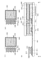
はじめに、基板100上に導電膜102を形成する(図1(A)参照)。
First, the
基板100は、絶縁表面を有する基板であればよく、例えば、ガラス基板とすることができる。ガラス基板は無アルカリガラス基板であることが好ましい。無アルカリガラス基板には、例えば、アルミノシリケートガラス、アルミノホウケイ酸ガラス、バリウムホウケイ酸ガラス等のガラス材料が用いられる。他にも、基板100として、セラミック基板、石英基板やサファイア基板等の絶縁体でなる絶縁性基板、シリコン等の半導体材料でなる半導体基板の表面を絶縁材料で被覆したもの、金属やステンレス等の導電体でなる導電性基板の表面を絶縁材料で被覆したものを用いることができる。また、作製工程の熱処理に耐えられるのであれば、プラスチック基板を用いることもできる。
The
導電膜102は、アルミニウム(Al)、銅(Cu)、モリブデン(Mo)、タングステン(W)、チタン(Ti)等の導電性材料で形成することが望ましい。形成方法としては、スパッタリング法や真空蒸着法、プラズマCVD法などがある。なお、導電膜102にアルミニウム(または銅)を用いる場合、アルミニウム単体(または銅単体)では耐熱性が低く、腐蝕しやすい等の問題があるため、耐熱性導電性材料と組み合わせて形成することが好ましい。
The
耐熱性導電性材料としては、チタン(Ti)、タンタル(Ta)、タングステン(W)、モリブデン(Mo)、クロム(Cr)、ネオジム(Nd)、スカンジウム(Sc)から選ばれた元素を含む金属、上述した元素を成分とする合金、上述した元素を組み合わせた合金、または上述した元素を成分とする窒化物などを用いることができる。これらの耐熱性導電性材料とアルミニウム(または銅)を積層させて、導電膜102を形成すればよい。
As a heat-resistant conductive material, a metal containing an element selected from titanium (Ti), tantalum (Ta), tungsten (W), molybdenum (Mo), chromium (Cr), neodymium (Nd), and scandium (Sc) An alloy containing the above-described element as a component, an alloy combining the above-described elements, or a nitride containing the above-described element as a component can be used. The
図示しないが、基板100上には下地層を設けても良い。下地層は、基板100からのアルカリ金属(Li、Cs、Na等)やアルカリ土類金属(Ca、Mg等)、その他の不純物の拡散を防止する機能を有する。つまり、下地層を設けることにより、半導体装置の信頼性向上という課題を解決することができる。下地層は、窒化シリコン、酸化シリコンなどの各種絶縁材料を用いて、単層構造または積層構造で形成すればよい。具体的には、例えば、基板100側から窒化シリコンと酸化シリコンを順に積層した構成とすることが好適である。窒化シリコンは、不純物に対するブロッキング効果が高いためである。一方で、窒化シリコンが半導体と接する場合には、半導体素子に不具合が発生する可能性もあるため、半導体と接する材料としては、酸化シリコンを適用するのがよい。
Although not shown, a base layer may be provided on the
次に、導電膜102上に選択的にレジストマスク104を形成し、該レジストマスク104を用いて導電膜102を選択的にエッチングすることで、ゲート電極として機能する導電層106を形成する(図1(B)参照)。
Next, a resist
レジストマスク104は、レジスト材料の塗布、フォトマスクを用いた露光、現像、等の工程を経ることにより形成される。レジスト材料の塗布は、スピンコート法などの方法を適用することができる。また、レジストマスク104は、液滴吐出法やスクリーン印刷法などを用いて選択的に形成しても良い。この場合、フォトマスクを用いた露光、現像等の工程が不要になるため、生産性向上という課題を解決することが可能である。なお、レジストマスク104は、導電膜102のエッチングにより導電層106が形成された後には除去される。
The resist
上述のエッチングには、ドライエッチングを用いても良いし、ウエットエッチングを用いても良い。また、後に形成されるゲート絶縁層等の被覆性を向上し、段切れを防止するために、導電層106の端部がテーパー形状となるようエッチングすると良い。例えば、テーパー角が20°以上90°未満となるような形状とすることが好ましい。ここで、「テーパー角」とは、テーパー形状を有する層を断面方向から観察した際に、当該層の側面と底面とがなす鋭角をいう。
As the above-described etching, dry etching or wet etching may be used. In order to improve coverage with a gate insulating layer or the like to be formed later and to prevent disconnection, etching is preferably performed so that the end portion of the
次に、導電層106を覆うように、ゲート絶縁層として機能する絶縁層108を形成する(図1(C)参照)。絶縁層108は、酸化シリコン、酸化窒化シリコン、窒化シリコン、窒化酸化シリコン、酸化アルミニウム、酸化タンタル等の材料を用いて形成することができる。また、これらの材料からなる膜を積層させて形成しても良い。これらの膜は、スパッタリング法等を用いて厚さが5nm以上250nm以下となるように形成すると好ましい。例えば、絶縁層108として、スパッタリング法を用いて、酸化シリコン膜を100nmの厚さで形成することができる。
Next, an insulating
他の方法(プラズマCVD法など)を用いて絶縁層108を形成する場合には、膜中の水素や窒素などの影響を考慮すべきであるが、所定の絶縁層108が得られるのであれば、作製方法については特に限定されない。例えば、絶縁層108中の水素濃度、窒素濃度が、後に形成される酸化物半導体層中より低いことを目安とすればよい。より具体的には、絶縁層108中の水素の濃度が1×10²¹atoms/cm3以下(好ましくは、5×1020atoms/cm3以下)、絶縁層108中の窒素の濃度が1×1019atoms/cm3以下とすれば良い。なお、良好な特性の絶縁層108を得るためには、成膜の温度条件は400℃以下とすることが望ましいが、開示する発明の一形態がこれに限定して解釈されるものではない。また、上記濃度は、絶縁層108中での平均値を示している。
When the insulating
また、スパッタリング法とCVD法(プラズマCVD法など)とを組み合わせて、積層構造の絶縁層108を形成しても良い。例えば、絶縁層108の下層(導電層106と接する領域)をプラズマCVD法により形成し、絶縁層108の上層をスパッタリング法により形成することができる。プラズマCVD法は、段差被覆性の良い膜を形成することが容易であるため、導電層106の直上に形成する膜を形成する方法として適している。また、スパッタリング法では、プラズマCVD法と比較して、膜中の水素濃度を低減することが容易であるため、スパッタリング法による膜を酸化物半導体層と接する領域に設けることで、絶縁層108中の水素が酸化物半導体層中へ拡散することを防止できる。酸化物半導体層内もしくはその近傍に存在する水素の半導体特性に与える影響は極めて大きいため、このような構成を採用することは効果的である。
Alternatively, the insulating
なお、本明細書等において、酸化窒化物とは、その組成において、窒素よりも酸素の含有量(原子数)が多いものを示し、例えば、酸化窒化シリコンとは、酸素が50原子%以上70原子%以下、窒素が0.5原子%以上15原子%以下、シリコンが25原子%以上35原子%以下、水素が0.1原子%以上10原子%以下の範囲で含まれるものをいう。また、窒化酸化物とは、その組成において、酸素よりも窒素の含有量(原子数)が多いものを示し、例えば、窒化酸化シリコンとは、酸素が5原子%以上30原子%以下、窒素が20原子%以上55原子%以下、シリコンが25原子%以上35原子%以下、水素が10原子%以上25原子%以下の範囲で含まれるものをいう。但し、上記範囲は、ラザフォード後方散乱法(RBS:Rutherford Backscattering Spectrometry)や、水素前方散乱法(HFS:Hydrogen Forward Scattering)を用いて測定した場合のものである。また、構成元素の含有比率の合計は100原子%を超えない。 Note that in this specification and the like, the term “oxynitride” refers to a composition whose oxygen content (number of atoms) is higher than that of nitrogen. For example, silicon oxynitride refers to oxygen at 50 atomic% or more and 70 It includes atoms in a range of not more than atomic%, nitrogen not less than 0.5 atom% and not more than 15 atom%, silicon not less than 25 atom% and not more than 35 atom%, and hydrogen not less than 0.1 atom% and not more than 10 atom%. In addition, a nitrided oxide indicates a composition whose nitrogen content (number of atoms) is higher than that of oxygen. For example, silicon nitride oxide refers to an oxygen content of 5 atomic% to 30 atomic% and nitrogen content. It includes 20 atomic% to 55 atomic%, silicon 25 atomic% to 35 atomic%, and hydrogen 10 atomic% to 25 atomic%. However, the above ranges are those measured using Rutherford Backscattering Spectrometry (RBS) or Hydrogen Forward Scattering (HFS). Further, the total content ratio of the constituent elements does not exceed 100 atomic%.
つづいて、絶縁層108に対し、第一のプラズマ処理を行う。当該処理は、酸素、またはハロゲン、またはそれらの内の2元素以上を含むプラズマを発生させて行う。プラズマを発生させる方式として、電子サイクロトン共鳴プラズマ(ECR:Electron Cyclotron Resonance Plasma)方式、ヘリコン波励起プラズマ(HWP:Helicon Wave Plasma)方式、誘導結合型プラズマ(ICP:Inductively Coupled Plasma)方式、マイクロ波励起表面波プラズマ(SWP:Surface Wave Plasma)方式などがある。これらの方式では、放電パワーによるイオンフラックスの制御と、バイアスパワーによるイオンエネルギーをそれぞれ独立で制御でき、1×10¹¹ions/cm3以上1×1013ions/cm3以下程度の高い電子密度が得られる。このとき、基板100には負のバイアスがかかっているため、絶縁層108に導入されるイオンは陽イオンのみである。代表的には、O+、O2+、O3+、O4+、O5+、O6+などの酸素イオン、Cl+、Cl2+、Cl3+、Cl4+、Cl5+、Cl6+、Cl7+などの塩素イオン、F+、F2+、F3+、F4+、F5+、F6+、F7+などのフッ素イオンなどが絶縁層108に注入される。
Subsequently, a first plasma treatment is performed on the insulating
プラズマのエネルギーを高くすることにより、低い価数の陽イオンに加え、高い価数の陽イオンが生成される。高い価数の陽イオンはより高いエネルギーを持って絶縁層108に注入されるため、低い価数の陽イオンと比較して、絶縁層108の表面からより深い位置に添加される。その深さは価数におおよそ比例する。これにより、陽イオンは絶縁層108に対してより一様な分布で添加されるため好ましい。具体的には、1価の陽イオンが深さdあたりにピークを持つ分布を形成するのであれば、2価の陽イオンは深さ2dあたりにピークを形成する。同様に3価、4価と価数が増えるに従って、ピーク位置も3d、4dと深くなる。また、当該ピーク位置が深くなるに伴い、分布も広がる傾向にある。従って、例えば、d=10nmの場合、厚さ50nmの絶縁層108に対しては、2価以上好ましくは4価以上の陽イオンを含むプラズマを形成し、添加することが好ましい。厚さ70nmの絶縁層108に対しては、3価以上好ましくは6価以上の陽イオンを含むプラズマを形成し、添加することが好ましい。陽イオンを添加する層の厚さtと、含まれると好ましい陽イオンの価数nとの関係式を以下に示す。n=[t/2d]、好ましくは、n=2×[t/2d]である。なお、[x]は、xを超えない最大の整数を示す。
By increasing the plasma energy, high valence cations are generated in addition to low cation cations. Since the high valence cation is injected into the insulating
このような高い価数の陽イオンを生成するためには、プラズマの電子温度を5eV以上100eV以下とすればよい。また、陽イオンの添加の際、基板温度を100℃以上500℃以下とすることで、同時に添加される水素の量を抑えることができるため好ましい。基板温度を高温にすればするほど絶縁層108からの水素の脱離が顕著となるためである。しかし、500℃以上の高温としてしまうと、低温で作製可能な酸化物半導体素子の特長を損なうため好ましくない。また、当該熱処理後、冷却速度を高める工程を入れてもよい。なお、当該第一のプラズマ処理は室温(本明細書中では25℃と定義する)で行ってもよく、室温より低い温度にて行ってもよい。
In order to generate such high valence cations, the electron temperature of the plasma may be 5 eV or more and 100 eV or less. In addition, when the cation is added, it is preferable to set the substrate temperature to 100 ° C. or more and 500 ° C. or less because the amount of hydrogen added simultaneously can be suppressed. This is because desorption of hydrogen from the insulating
本実施の形態において、上記第一のプラズマ処理に、誘導結合型プラズマ(ICP)方式を採用した。推奨される処理条件の一例は、ICPへの投入電力100W以上2000W以下、基板側に設けられる下部電極への投入電力0W以上300W以下、処理時間10秒以上100秒以下、処理チャンバー内圧力0.1Pa以上100Pa以下、酸素(O2)流量10sccm以上500sccm以下、下部電極温度−20℃以上500℃以下、ICPのRF電源周波数13.56MHzである。なお、下部電極温度は基板に伝わるため、基板温度が500℃を超えないようにする。また、下部電極へ電力を投入する場合、下部電極に与えるRF電源周波数は、3.2MHzまたは13.56MHzを推奨する。なお、酸素(O2)の代わりにフッ素や塩素などのハロゲンを同程度の流量にて流してもよい。また、これらの元素を2元素以上含む気体を流してもよい。 In this embodiment, an inductively coupled plasma (ICP) method is employed for the first plasma treatment. Examples of recommended processing conditions are: input power to the ICP of 100 W to 2000 W, input power to the lower electrode provided on the substrate side of 0 W to 300 W, processing time of 10 seconds to 100 seconds, processing chamber pressure of 0. 1 Pa to 100 Pa, oxygen (O 2 ) flow rate of 10 sccm to 500 sccm, lower electrode temperature of −20 ° C. to 500 ° C., and ICP RF power frequency of 13.56 MHz. Since the lower electrode temperature is transmitted to the substrate, the substrate temperature should not exceed 500 ° C. In addition, when power is supplied to the lower electrode, it is recommended that the RF power supply frequency applied to the lower electrode is 3.2 MHz or 13.56 MHz. Note that halogen such as fluorine or chlorine may be supplied at a similar flow rate instead of oxygen (O 2 ). Further, a gas containing two or more of these elements may be flowed.
次に、絶縁層108を覆うように酸化物半導体膜110を形成する(図1(D)参照)。本実施の形態においては、酸化物半導体膜110に金属酸化物半導体材料を用いる。
Next, the
酸化物半導体層としては、少なくともIn、Ga、Sn、Zn、Al、Mg、Hf及びランタノイドから選ばれた一種以上の元素を含有する。例えば、四元系金属の酸化物であるIn−Sn−Ga−Zn−O系酸化物半導体や、三元系金属の酸化物であるIn−Ga−Zn−O系酸化物半導体、In−Sn−Zn−O系酸化物半導体、In−Al−Zn−O系酸化物半導体、Sn−Ga−Zn−O系酸化物半導体、Al−Ga−Zn−O系酸化物半導体、Sn−Al−Zn−O系酸化物半導体、In−Hf−Zn−O系酸化物半導体、In−La−Zn−O系酸化物半導体、In−Ce−Zn−O系酸化物半導体、In−Pr−Zn−O系酸化物半導体、In−Nd−Zn−O系酸化物半導体、In−Pm−Zn−O系酸化物半導体、In−Sm−Zn−O系酸化物半導体、In−Eu−Zn−O系酸化物半導体、In−Gd−Zn−O系酸化物半導体、In−Tb−Zn−O系酸化物半導体、In−Dy−Zn−O系酸化物半導体、In−Ho−Zn−O系酸化物半導体、In−Er−Zn−O系酸化物半導体、In−Tm−Zn−O系酸化物半導体、In−Yb−Zn−O系酸化物半導体、In−Lu−Zn−O系酸化物半導体や、二元系金属の酸化物であるIn−Zn−O系酸化物半導体、Sn−Zn−O系酸化物半導体、Al−Zn−O系酸化物半導体、Zn−Mg−O系酸化物半導体、Sn−Mg−O系酸化物半導体、In−Mg−O系酸化物半導体や、In−Ga−O系の材料、一元系金属の酸化物であるIn−O系酸化物半導体、Sn−O系酸化物半導体、Zn−O系酸化物半導体などを用いることができる。また、上記酸化物半導体にInとGaとSnとZnとAlとMgとHf及びランタノイド以外の元素、例えばSiO2を含ませてもよい。 The oxide semiconductor layer contains at least one element selected from In, Ga, Sn, Zn, Al, Mg, Hf, and a lanthanoid. For example, an In—Sn—Ga—Zn—O-based oxide semiconductor that is an oxide of a quaternary metal, an In—Ga—Zn—O-based oxide semiconductor that is an oxide of a ternary metal, or In—Sn -Zn-O-based oxide semiconductor, In-Al-Zn-O-based oxide semiconductor, Sn-Ga-Zn-O-based oxide semiconductor, Al-Ga-Zn-O-based oxide semiconductor, Sn-Al-Zn -O-based oxide semiconductor, In-Hf-Zn-O-based oxide semiconductor, In-La-Zn-O-based oxide semiconductor, In-Ce-Zn-O-based oxide semiconductor, In-Pr-Zn-O Oxide semiconductor, In—Nd—Zn—O oxide semiconductor, In—Pm—Zn—O oxide semiconductor, In—Sm—Zn—O oxide semiconductor, In—Eu—Zn—O oxide Semiconductor, In-Gd-Zn-O-based oxide semiconductor, In-Tb-Zn-O-based oxidation Semiconductor, In-Dy-Zn-O-based oxide semiconductor, In-Ho-Zn-O-based oxide semiconductor, In-Er-Zn-O-based oxide semiconductor, In-Tm-Zn-O-based oxide semiconductor, In-Yb-Zn-O-based oxide semiconductor, In-Lu-Zn-O-based oxide semiconductor, In-Zn-O-based oxide semiconductor that is an oxide of a binary metal, Sn-Zn-O-based Oxide semiconductor, Al-Zn-O-based oxide semiconductor, Zn-Mg-O-based oxide semiconductor, Sn-Mg-O-based oxide semiconductor, In-Mg-O-based oxide semiconductor, In-Ga-O For example, an In—O-based oxide semiconductor, a Sn—O-based oxide semiconductor, or a Zn—O-based oxide semiconductor that is an oxide of a single metal can be used. The oxide semiconductor may contain elements other than In, Ga, Sn, Zn, Al, Mg, Hf, and lanthanoid, for example, SiO 2 .
例えば、In―Ga―Zn―O系酸化物半導体とは、インジウム(In)、ガリウム(Ga)、亜鉛(Zn)を有する酸化物半導体、という意味であり、その組成比は問わない。 For example, an In—Ga—Zn—O-based oxide semiconductor means an oxide semiconductor containing indium (In), gallium (Ga), and zinc (Zn), and there is no limitation on the composition ratio.
上記酸化物半導体材料の一例としては、InMO3(ZnO)m(m>0)で表記されるものがある。ここで、Mは、亜鉛(Zn)、ガリウム(Ga)、鉄(Fe)、ニッケル(Ni)、マンガン(Mn)、コバルト(Co)などから選ばれた一の金属元素または複数の金属元素を示す。例えばMとしてGaが選択される場合には、Gaのみの場合の他に、GaとNiや、GaとFeなど、Ga以外の上記金属元素が選択される場合を含む。また、上記酸化物半導体において、Mとして含まれる金属元素の他に、不純物元素としてFe、Niその他の遷移金属元素、または該遷移金属の酸化物が含まれているものがある。もちろん、酸化物半導体材料は上記の材料に限定されず、酸化亜鉛や酸化インジウムをはじめとする各種酸化物半導体材料を用いることができる。 As an example of the oxide semiconductor material, there is a material represented by InMO 3 (ZnO) m (m> 0). Here, M represents one metal element or a plurality of metal elements selected from zinc (Zn), gallium (Ga), iron (Fe), nickel (Ni), manganese (Mn), cobalt (Co), and the like. Show. For example, the case where Ga is selected as M includes the case where the above metal element other than Ga, such as Ga and Ni or Ga and Fe, is selected in addition to the case of Ga alone. In addition to the metal element contained as M, some of the above oxide semiconductors contain Fe, Ni, other transition metal elements, or oxides of the transition metal as impurity elements. Needless to say, the oxide semiconductor material is not limited to the above materials, and various oxide semiconductor materials including zinc oxide and indium oxide can be used.
酸化物半導体材料としてIn−Ga−Zn−O系の材料を用いて酸化物半導体膜110を形成する場合には、例えば、In、Ga、Znを含む酸化物半導体ターゲット(In2O3:Ga2O3:ZnO=1:1:1)を用いたスパッタリング法で形成することができる。該スパッタリングは、例えば、基板100とターゲットとの距離を30mm〜500mm、圧力を0.1Pa〜2.0Pa、直流(DC)電源を0.25kW〜5.0kW、温度を20℃〜100℃、雰囲気をアルゴン等の希ガス雰囲気、酸素雰囲気、またはアルゴン等の希ガスと酸素との混合雰囲気とする条件で行うことができる。また、上記のスパッタリング法としては、スパッタリング用電源に高周波電源を用いるRFスパッタリング法や、直流電源を用いるDCスパッタリング法、パルス的に直流バイアスを加えるパルスDCスパッタリング法などを用いることができる。
In the case where the
また、酸化物半導体としてIn−Zn−O系の材料を用いる場合、用いるターゲットの組成比は、原子数比で、In:Zn=50:1〜1:2(モル数比に換算するとIn2O3:ZnO=25:1〜1:4)、好ましくはIn:Zn=20:1〜1:1(モル数比に換算するとIn2O3:ZnO=10:1〜1:2)、さらに好ましくはIn:Zn=15:1〜1.5:1(モル数比に換算するとIn2O3:ZnO=15:2〜3:4)とする。例えば、In−Zn−O系酸化物半導体の形成に用いるターゲットは、原子数比がIn:Zn:O=X:Y:Zのとき、Z>1.5X+Yとする。 In the case where an In—Zn—O-based material is used as the oxide semiconductor, the composition ratio of the target used is an atomic ratio, and In: Zn = 50: 1 to 1: 2 (in terms of the molar ratio, In 2 O 3 : ZnO = 25: 1 to 1: 4), preferably In: Zn = 20: 1 to 1: 1 (In 2 O 3 : ZnO = 10: 1 to 1: 2 in terms of molar ratio), More preferably, In: Zn = 15: 1 to 1.5: 1 (In 2 O 3 : ZnO = 15: 2 to 3: 4 in terms of molar ratio). For example, a target used for forming an In—Zn—O-based oxide semiconductor satisfies Z> 1.5X + Y when the atomic ratio is In: Zn: O = X: Y: Z.
本実施の形態においては、酸化物半導体膜110を単層で形成する場合について示しているが、酸化物半導体膜110は、積層構造としても良い。例えば、絶縁層108上に、酸化物半導体膜110と同様の組成の酸化物半導体膜(以下「通常の導電性の酸化物半導体膜」と呼ぶ)を形成し、その後、酸化物半導体膜110と構成元素が同じでその構成比率が異なる酸化物半導体膜(以下「導電性の高い酸化物半導体膜」と呼ぶ)を形成して、上記構成に代えることができる。この場合、導電性の高い酸化物半導体膜をソース電極(またはドレイン電極)と通常の導電性の酸化物半導体膜との間に設けることになるため、素子特性の向上につながる。
Although this embodiment shows the case where the
通常の導電性の酸化物半導体膜と、導電性の高い酸化物半導体膜とは、例えば、成膜条件を異ならせることで形成することができる。この場合、導電性の高い酸化物半導体膜の成膜条件は、通常の導電性の酸化物半導体膜の成膜条件より、アルゴンガスの流量に対する酸素ガスの流量を小さいものとすると良い。より具体的には、導電性の高い酸化物半導体膜の成膜条件は、希ガス(アルゴン、又はヘリウムなど)雰囲気下、または、酸素ガス10%以下、希ガス90%以上の雰囲気下とし、通常の導電性の酸化物半導体膜の成膜条件は、酸素雰囲気下、または、希ガスに対する酸素ガスの流量比が1以上の雰囲気下とする。このようにすることで、導電性の異なる2種類の酸化物半導体膜を形成することができる。 A normal conductive oxide semiconductor film and a highly conductive oxide semiconductor film can be formed, for example, by different film formation conditions. In this case, the deposition condition of the highly conductive oxide semiconductor film is preferably set so that the flow rate of the oxygen gas is smaller than the deposition condition of the normal conductive oxide semiconductor film. More specifically, the film formation condition of the highly conductive oxide semiconductor film is a rare gas (argon, helium, or the like) atmosphere or an oxygen gas atmosphere of 10% or less and a rare gas atmosphere of 90% or more. The conditions for forming a normal conductive oxide semiconductor film are an oxygen atmosphere or an atmosphere having a flow ratio of oxygen gas to a rare gas of 1 or more. Thus, two types of oxide semiconductor films having different conductivity can be formed.
また、プラズマ処理を行った後、大気に曝すことなく酸化物半導体膜110を形成する場合には、絶縁層108と酸化物半導体膜110の界面にゴミや水分が付着することを抑制することができる。
In addition, in the case where the
なお、酸化物半導体膜110の膜厚は、5nm〜200nm程度とすればよい。
Note that the thickness of the
つづいて、酸化物半導体膜110に対し、第二のプラズマ処理を行う。図1(D)中の+の記号は陽イオンを示す。当該処理は、第一のプラズマ処理と同様の方法を用いて行うことができる。なお、当該第二のプラズマ処理は、酸化物半導体膜110の露出している段階で行えばよいため、必ずしもこの段階で行う必要はない。当該プラズマ処理を行うことで、半導体素子の特性を飛躍的に向上させ、また、特性ばらつきを低減させることができる。
Subsequently, a second plasma treatment is performed on the
また、酸化物半導体膜110をm層の多層構造とする場合、例えば第1層から(m−1)層を形成後のいずれかの段階において、第二のプラズマ処理を行ってもよい。また、当該第二のプラズマ処理での熱処理後、冷却速度を高める工程を入れてもよい。なお、当該第二のプラズマ処理は室温で行ってもよく、室温より低い温度にて行ってもよい。
In the case where the
次に、酸化物半導体膜110上に選択的にレジストマスク112を形成し、該レジストマスク112を用いて酸化物半導体膜110を選択的にエッチングすることで、酸化物半導体層114を形成する(図1(E)参照)。ここで、レジストマスク112は、レジストマスク104と同様の方法で形成することができる。また、レジストマスク112は、酸化物半導体膜110のエッチングにより酸化物半導体層114が形成された後には除去される。
Next, a resist
酸化物半導体膜110のエッチングの方法としては、ウエットエッチングまたはドライエッチングを用いることができる。ここでは、酢酸と硝酸と燐酸との混合液を用いたウエットエッチングにより、酸化物半導体膜110の不要な部分を除去して、酸化物半導体層114を形成する。なお、上記のウエットエッチングに用いることができるエッチャント(エッチング液)は酸化物半導体膜110をエッチングできるものであればよく、上述したものに限られない。
As a method for etching the
ドライエッチングを行う場合は、例えば、塩素原子を含有するガス(例えば、塩素(Cl2)、二酸化塩素(ClO2)など)または塩素原子を含有するガスに酸素(O2)が添加されたガスを用いると良い。塩素原子を含有するガスを用いることで、導電層や下地層と、酸化物半導体膜110とのエッチング選択比がとりやすくなるためである。
In the case of performing dry etching, for example, a gas containing chlorine atoms (for example, chlorine (Cl 2 ), chlorine dioxide (ClO 2 ), etc.) or a gas in which oxygen (O 2 ) is added to a gas containing chlorine atoms. It is good to use. This is because by using a gas containing chlorine atoms, an etching selectivity between the conductive layer or the base layer and the
ドライエッチングには、反応性イオンエッチング法(RIE法)を用いたエッチング装置や、ECR(Electron Cyclotron Resonance)やICP(Inductively Coupled Plasma)などの高密度プラズマ源を用いたドライエッチング装置を用いることができる。また、それらに類似した技術を用いてもよい。 For the dry etching, an etching apparatus using a reactive ion etching method (RIE method) or a dry etching apparatus using a high-density plasma source such as ECR (Electron Cyclotron Resonance) or ICP (Inductively Coupled Plasma) is used. it can. Moreover, you may use the technique similar to them.
次に、絶縁層108および酸化物半導体層114を覆うように、導電膜116を形成する(図2(A)参照)。導電膜116は、導電膜102と同様の材料、方法によって形成することができる。例えば、導電膜116を、モリブデン膜やチタン膜の単層構造で形成することができる。また、導電膜116を積層構造で形成してもよく、例えば、アルミニウム膜とチタン膜との積層構造とすることができる。また、チタン膜と、アルミニウム膜と、チタン膜とを順に積層した3層構造としてもよい。また、モリブデン膜とアルミニウム膜とモリブデン膜とを順に積層した3層構造としてもよい。また、これらの積層構造に用いるアルミニウム膜として、ネオジムを含むアルミニウム(Al−Nd)膜を用いてもよい。さらに、導電膜116を、シリコンを含むアルミニウムの単層構造としてもよい。
Next, the
次に、導電膜116上に選択的にレジストマスク118およびレジストマスク120を形成し、該レジストマスクを用いて導電膜116を選択的にエッチングすることで、ソース電極またはドレイン電極の一方として機能する導電層122およびソース電極またはドレイン電極の他方として機能する導電層124を形成する(図2(B)参照)。ここで、レジストマスク118およびレジストマスク120は、レジストマスク104と同様の方法で形成することができる。また、レジストマスク118およびレジストマスク120は、導電膜116のエッチングにより導電層122および導電層124が形成された後には除去される。
Next, a resist
レジストマスク118は、多階調マスクを用いて形成しても良い。ここで、多階調マスクとは、多段階の光量で露光を行うことが可能なマスクをいう。これを用いることで、一度の露光および現像工程によって、複数(代表的には2種類)の厚さのレジストマスクを形成することができる。つまり、多階調マスクを用いることで、工程数の増加を抑制することができる。
The resist
導電膜116のエッチングの方法としては、ウエットエッチングまたはドライエッチングを用いることができる。ここでは、ドライエッチングにより導電膜116の不要な部分を除去して、導電層122および導電層124を形成する。
As a method for etching the
なお、本実施の形態においては、上記導電膜116のエッチングの際に酸化物半導体層114の一部が除去される構成(チャネルエッチ型)としているが、開示する発明の一形態はこれに限定されない。エッチングの進行を停止させる層(エッチストッパ)を酸化物半導体層114と導電膜116との間に形成して、酸化物半導体層114がエッチングされない構成(エッチストップ型)とすることもできる。
Note that in this embodiment, the
導電層122および導電層124を形成した後には、100℃〜500℃、代表的には200℃〜400℃の熱処理を行う。熱処理の雰囲気は、例えば、大気雰囲気や窒素雰囲気、酸素雰囲気等とすることができる。また、熱処理時間は、0.1時間〜5時間程度とすればよい。ここでは、大気雰囲気下で350℃、1時間の熱処理を行うこととする。なお、該熱処理のタイミングは、酸化物半導体膜110を形成した後、層間絶縁層にあたる絶縁層を形成する前であれば特に限定されない。例えば、酸化物半導体膜110を形成した直後に上記の熱処理を行っても良い。また、酸化物半導体層114を形成した直後や、導電膜116を形成した直後であっても良い。当該熱処理(第1の熱処理)と後の熱処理(第2の熱処理)とを行うことで、半導体素子の特性を向上させ、また、特性ばらつきを低減させることができる。
After the
なお、上記熱処理の条件を400℃以下とすることは、ゲート絶縁層として機能する絶縁層108の特性を変化させない(劣化させない)ために好適である。もちろん、開示する発明の一形態がこれに限定して解釈されるものではない。
Note that it is preferable that the heat treatment be performed at 400 ° C. or lower in order not to change (deteriorate) the characteristics of the insulating
次に、導電層122、導電層124、酸化物半導体層114などを覆うように絶縁層126を形成する(図2(C)参照)。ここで、絶縁層126は、いわゆる層間絶縁層にあたる。絶縁層126は、酸化シリコン、酸化アルミニウム、酸化タンタル等の材料を用いて形成することができる。また、これらの材料からなる膜を積層させて形成しても良い。
Next, the insulating
絶縁層126中の水素の濃度が1×10²¹atoms/cm3以下(特に、5×1020atoms/cm3以下)であると好ましい。また、絶縁層126中の窒素の濃度が1×1019atoms/cm3以下であると好ましい。なお、上記濃度は、絶縁層126中での平均値を示している。
It is preferable that the concentration of hydrogen in the insulating
上述のような条件を満たす絶縁層126のより具体的な一例として、スパッタリング法により形成された酸化シリコン膜を挙げることができる。スパッタリング法を用いる場合には、プラズマCVD法を用いる場合と比較して、膜中の水素濃度の低減が容易になるためである。もちろん、上述の条件を満たすのであれば、プラズマCVD法を含む他の方法により形成しても良い。例えば、プラズマCVD法にて絶縁層126を形成後、絶縁層108に対して行ったのと同様のプラズマ処理を当該絶縁層126に施して、膜中の水素濃度を下げることができる。絶縁層126のその他の条件については、特に限定されない。例えば、絶縁層126の厚さについては、実現可能な範囲であればどのような値をとっても良い。
As a more specific example of the insulating
その後、各種電極や配線を形成することでトランジスタ150を具備する半導体装置が完成する(図2(D)参照)。本実施の形態においては代表的に、表示装置の画素電極として機能する導電層128を形成する例について示すが、開示する発明の一形態はこれに限定されない。
After that, by forming various electrodes and wirings, a semiconductor device including the
導電層128を形成した後には、100℃〜500℃、代表的には200℃〜400℃の熱処理を行う。熱処理の雰囲気は、例えば、大気雰囲気や窒素雰囲気、酸素雰囲気等とすることができる。また、熱処理時間は、0.1時間〜5時間程度とすればよい。ここでは、大気雰囲気下で350℃、1時間の熱処理を行うこととする。なお、該熱処理のタイミングは、絶縁層126を形成した後であれば特に限定されない。例えば、絶縁層126を形成した直後に上記の熱処理を行っても良いし、さらに他の絶縁層や導電層などを形成した後に、上記の熱処理を行っても良い。当該熱処理(第2の熱処理)と先の熱処理(第1の熱処理)とを行うことによって、半導体素子の特性を向上させ、また、特性ばらつきを低減させることができる。
After the
なお、第2の熱処理の効果は、上述のものに留まらない。例えば、第2の熱処理は、絶縁層126の欠陥を修復するという効果をも有している。絶縁層126は比較的低温で形成されるため、膜中には欠陥が存在しており、そのまま使用した場合には素子特性に悪影響を及ぼすおそれがある。このような絶縁層126中の欠陥を修復するという観点からも、上述の熱処理は重要な役割を果たすと言える。
Note that the effect of the second heat treatment is not limited to the above. For example, the second heat treatment also has an effect of repairing defects in the insulating
また、上記熱処理の条件を400℃以下とすることは、ゲート絶縁層として機能する絶縁層108の特性を変化させない(劣化させない)ために好適である。もちろん、開示する発明の一形態がこれに限定して解釈されるものではない。
In addition, it is preferable that the heat treatment condition is 400 ° C. or lower in order not to change (deteriorate) the characteristics of the insulating
本実施の形態において示すように、酸化物半導体膜110に陽イオンによるプラズマ処理を施すことにより、優れた特性の酸化物半導体素子を提供することができる。当該処理は、酸化物半導体膜110に接する絶縁層108または絶縁層126またはそれらの両方にも行うことにより、より信頼性の高い半導体素子を得ることができる。これにより、優れた特性の酸化物半導体素子を備えた半導体装置を提供することができる。
As described in this embodiment, an oxide semiconductor element with excellent characteristics can be provided by performing plasma treatment with positive ions on the
本実施の形態は他の実施の形態と適宜組み合わせることができる。 This embodiment can be combined with any of the other embodiments as appropriate.
(実施の形態2)
本実施の形態では、半導体装置に用いられる半導体素子の作製方法につき、上記実施の形態と異なる一例について図面を参照して説明する。なお、本実施の形態における半導体装置の作製工程は、多くの部分で先の実施の形態と共通している。したがって、以下においては、重複する部分の説明は省略し、異なる点について詳細に説明する。
(Embodiment 2)
In this embodiment, an example of a method for manufacturing a semiconductor element used for a semiconductor device, which is different from that in the above embodiment, will be described with reference to drawings. Note that the manufacturing process of the semiconductor device in this embodiment mode is similar to that of the above embodiment mode in many parts. Therefore, in the following, description of overlapping parts is omitted, and different points will be described in detail.
はじめに、基板200上に導電膜202を形成する(図3(A)参照)。基板200、導電膜202、その他の詳細については、先の実施の形態(図1(A)の説明部分など)を参照すればよい。また、基板200上には下地層を設けても良い。下地層の詳細についても、先の実施の形態を参照することができる。
First, the
次に、導電膜202上に選択的にレジストマスク204を形成し、該レジストマスク204を用いて導電膜202を選択的にエッチングすることで、ゲート電極として機能する導電層206を形成する(図3(B)参照)。レジストマスク204、導電層206、エッチング、その他の詳細については、先の実施の形態(図1(B)の説明部分など)を参照することができる。
Next, a resist
次に、導電層206を覆うように、ゲート絶縁層として機能する絶縁層208を形成する(図3(C)参照)。絶縁層208、その他の詳細については、先の実施の形態(図1(C)の説明部分など)を参照すればよい。
Next, an insulating
つづいて、実施の形態1で示した第一のプラズマ処理と同様の処理を行う。当該プラズマ処理は、絶縁層208の少なくとも一部が露出している段階で行えばよく、必ずしもこの段階で行う必要はない。当該プラズマはマイクロ波により生成してもよい。このときの周波数は例えば、2.45GHzとする。
Subsequently, the same processing as the first plasma processing described in Embodiment 1 is performed. The plasma treatment may be performed at a stage where at least part of the insulating
次に、絶縁層208を覆うように導電膜210を形成する(図3(D)参照)。導電膜210は、導電膜202と同様の材料、方法によって形成することができる。つまり、詳細については、先の実施の形態(図1(A)、図2(A)の説明部分など)を参照すればよい。
Next, a
次に、導電膜210上に選択的にレジストマスク212およびレジストマスク214を形成し、該レジストマスクを用いて導電膜210を選択的にエッチングすることで、ソース電極またはドレイン電極の一方として機能する導電層216およびソース電極またはドレイン電極の他方として機能する導電層218を形成する(図3(E)参照)。レジストマスク212およびレジストマスク214は、レジストマスク204と同様にして形成することができる。つまり、レジストマスクの詳細については、先の実施の形態(図1(B)、図2(B)の説明部分など)を参照すればよい。
Next, a resist
導電膜210のエッチングの方法としては、ウエットエッチングまたはドライエッチングを用いることができる。ここでは、ドライエッチングにより導電膜210の不要な部分を除去して、導電層216および導電層218を形成する。なお、本実施の形態においては示していないが、当該エッチングにより絶縁層208の一部が除去されることがある。
As a method for etching the
次に、絶縁層208、導電層216、導電層218等を覆うように酸化物半導体膜220を形成する(図4(A)参照)。酸化物半導体膜220の詳細については、先の実施の形態(図1(D)の説明部分など)を参照することができる。
Next, the
つづいて、実施の形態1で示した第二のプラズマ処理と同様の処理を行う。図4(A)中の+の記号は陽イオンを示す。当該プラズマ処理は、酸化物半導体膜220の少なくとも一部が露出している段階で行えばよく、必ずしもこの段階で行う必要はない。当該プラズマはマイクロ波により生成してもよい。このときの周波数は例えば、2.45GHzとする。
Subsequently, the same processing as the second plasma processing described in Embodiment 1 is performed. The symbol “+” in FIG. 4A represents a cation. The plasma treatment may be performed when at least part of the
次に、酸化物半導体膜220上に選択的にレジストマスク222を形成し、該レジストマスク222を用いて酸化物半導体膜220を選択的にエッチングすることで、酸化物半導体層224を形成する(図4(B)参照)。レジストマスク222の詳細については、先の実施の形態(図1(B)、図1(E)の説明部分など)を参照すればよい。
Next, a resist
酸化物半導体膜220のエッチングの方法としては、ウエットエッチングまたはドライエッチングを用いることができる。ここでは、酢酸と硝酸と燐酸との混合液を用いたウエットエッチングにより、酸化物半導体膜220の不要な部分を除去して、酸化物半導体層224を形成する。なお、上記のウエットエッチングに用いることができるエッチャント(エッチング液)は酸化物半導体膜220をエッチングできるものであればよく、上述したものに限られない。
As a method for etching the
ドライエッチングを行う場合は、例えば、塩素原子を含有するガス(例えば、塩素(Cl2)、二酸化塩素(ClO2)など)または塩素原子を含有するガスに酸素(O2)が添加されたガスを用いると良い。塩素原子を含有するガスを用いることで、導電層や下地層と、酸化物半導体膜220とのエッチング選択比がとりやすくなるためである。なお、エッチングのその他の詳細については、先の実施の形態を参照すればよい。
In the case of performing dry etching, for example, a gas containing chlorine atoms (for example, chlorine (Cl 2 ), chlorine dioxide (ClO 2 ), etc.) or a gas in which oxygen (O 2 ) is added to a gas containing chlorine atoms. It is good to use. This is because by using a gas containing a chlorine atom, an etching selectivity between the conductive layer or the base layer and the
酸化物半導体層224を形成した後には、100℃〜500℃、代表的には200℃〜400℃の熱処理を行う。熱処理の雰囲気は、例えば、大気雰囲気や窒素雰囲気、酸素雰囲気等とすることができる。また、熱処理時間は、0.1時間〜5時間程度とすればよい。ここでは、大気雰囲気下で350℃、1時間の熱処理を行うこととする。なお、該熱処理のタイミングは、酸化物半導体膜220を形成した後、層間絶縁層にあたる絶縁層を形成する前であれば特に限定されない。例えば、酸化物半導体膜220を形成した直後に上記の熱処理を行っても良い。当該熱処理(第1の熱処理)と後の熱処理(第2の熱処理)とを行うことで、半導体素子の特性を向上させ、また、特性ばらつきを低減させることができる。
After the
なお、上記熱処理の条件を400℃以下とすることは、ゲート絶縁層として機能する絶縁層208の特性を変化させない(劣化させない)ために好適である。もちろん、開示する発明の一形態がこれに限定して解釈されるものではない。
Note that it is preferable that the heat treatment condition be 400 ° C. or lower in order not to change (deteriorate) the characteristics of the insulating
次に、導電層216、導電層218、酸化物半導体層224などを覆うように絶縁層226を形成する(図4(C)参照)。ここで、絶縁層226は、いわゆる層間絶縁層にあたる。絶縁層226は、酸化シリコン、酸化アルミニウム、酸化タンタル等の材料を用いて形成することができる。また、これらの材料からなる膜を積層させて形成しても良い。
Next, an insulating
つづいて、実施の形態1で示した第一のプラズマ処理と同様の処理を行う。当該プラズマ処理は、絶縁層226の少なくとも一部が露出している段階で行えばよく、必ずしもこの段階で行う必要はない。
Subsequently, the same processing as the first plasma processing described in Embodiment 1 is performed. The plasma treatment may be performed at a stage where at least part of the insulating
絶縁層226中の水素の濃度が1×10²¹atoms/cm3以下(特に、5×1020atoms/cm3以下)であると好ましい。また、絶縁層226中の窒素の濃度が1×1019atoms/cm3以下であると好ましい。なお、上記濃度は、絶縁層226中での平均値を示している。
The concentration of hydrogen in the insulating
上述のような条件を満たす絶縁層226のより具体的な一例として、スパッタリング法により形成された酸化シリコン膜を挙げることができる。スパッタリング法を用いる場合には、プラズマCVD法を用いる場合と比較して、膜中の水素濃度の低減が容易になるためである。もちろん、上述の条件を満たすのであれば、プラズマCVD法を含む他の方法により形成しても良い。例えば、プラズマCVD法にて絶縁層226を形成後、先の実施の形態1に示した絶縁層108に対して行ったのと同様のプラズマ処理を当該絶縁層226に施して、膜中の水素濃度を下げることができる。絶縁層226のその他の条件については、特に限定されない。例えば、絶縁層226の厚さについては、実現可能な範囲であればどのような値をとっても良い。
As a more specific example of the insulating
その後、各種電極や配線を形成することでトランジスタ250を具備する半導体装置が完成する(図4(D)参照)。本実施の形態においては代表的に、表示装置の画素電極として機能する導電層228を形成する例について示す(図4(D)参照)が、開示する発明の一形態はこれに限定されない。
After that, a semiconductor device including the
導電層228を形成した後には、100℃〜500℃、代表的には200℃〜400℃の熱処理を行う。熱処理の雰囲気は、例えば、大気雰囲気や窒素雰囲気、酸素雰囲気等とすることができる。また、熱処理時間は、0.1時間〜5時間程度とすればよい。ここでは、大気雰囲気下で350℃、1時間の熱処理を行うこととする。なお、該熱処理のタイミングは、絶縁層226を形成した後であれば特に限定されない。例えば、絶縁層226を形成した直後に上記の熱処理を行っても良いし、さらに他の絶縁層や導電層などを形成した後に、上記の熱処理を行っても良い。当該熱処理(第2の熱処理)と先の熱処理(第1の熱処理)とを行うことによって、半導体素子の特性を向上させ、また、特性ばらつきを低減させることができる。
After the
なお、第2の熱処理の効果は、上述のものに留まらない。例えば、第2の熱処理は、絶縁層226の欠陥を修復するという効果をも有している。絶縁層226は比較的低温で形成されるため、膜中には欠陥が存在しており、そのまま使用した場合には素子特性に悪影響を及ぼすおそれがある。このような絶縁層226中の欠陥を修復するという観点からも、上述の熱処理は重要な役割を果たすと言える。
Note that the effect of the second heat treatment is not limited to the above. For example, the second heat treatment also has an effect of repairing defects in the insulating
また、上記熱処理の条件を400℃以下とすることは、ゲート絶縁層として機能する絶縁層208の特性を変化させない(劣化させない)ために好適である。もちろん、開示する発明の一形態がこれに限定して解釈されるものではない。
In addition, it is preferable that the heat treatment condition be 400 ° C. or lower in order not to change (deteriorate) the characteristics of the insulating
本実施の形態において示すように、酸化物半導体膜220に陽イオンによるプラズマ処理を施すことにより、優れた特性の酸化物半導体素子を提供することができる。当該処理は、酸化物半導体膜220に接する絶縁層208または絶縁層226、またはそれらの両方にも行うことにより、より信頼性の高い半導体素子を得ることができる。これにより、優れた特性の酸化物半導体素子を備えた半導体装置を提供することができる。
As described in this embodiment, by performing plasma treatment with positive ions on the
なお、本実施の形態は、先の実施の形態と適宜組み合わせて用いることができる。 Note that this embodiment can be combined with any of the above embodiments as appropriate.
(実施の形態3)
本実施の形態では、半導体装置に用いられる半導体素子の作製方法の一例について、図面を参照して説明する。
(Embodiment 3)
In this embodiment, an example of a method for manufacturing a semiconductor element used for a semiconductor device will be described with reference to drawings.
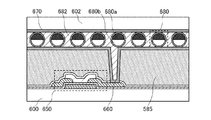
はじめに、基板500上に導電膜502を形成する(図5(A)参照)。導電膜502を形成する前に、絶縁体である基板500に対し、実施の形態1で示した第一のプラズマ処理と同様の処理を行ってもよい。当該プラズマ処理は、後に形成する酸化物半導体層508に接する基板の絶縁表面に施せばよいため、必ずしもこの段階で行う必要はない。また、後に説明する下地層501を基板500と導電膜502の間に絶縁層として形成する場合は、下地層501に対して行ってもよい。なお、当該プラズマはマイクロ波により生成してもよい。このときの周波数は例えば、2.45GHzとする。
First, a
基板500は、絶縁表面を有する基板であればよく、例えば、ガラス基板とすることができる。ガラス基板は無アルカリガラス基板であることが好ましい。無アルカリガラス基板には、例えば、アルミノシリケートガラス、アルミノホウケイ酸ガラス、バリウムホウケイ酸ガラス等のガラス材料が用いられる。他にも、基板500として、セラミック基板、石英基板やサファイア基板等の絶縁体でなる絶縁性基板、シリコン等の半導体材料でなる半導体基板の表面を絶縁材料で被覆したもの、金属やステンレス等の導電体でなる導電性基板の表面を絶縁材料で被覆したものを用いることができる。また、作製工程の熱処理に耐えられるのであれば、プラスチック基板を用いることもできる。
The
導電膜502は、アルミニウム(Al)、銅(Cu)、モリブデン(Mo)、タングステン(W)、チタン(Ti)等の導電性材料で形成することが望ましい。形成方法としては、スパッタリング法や真空蒸着法、プラズマCVD法などがある。なお、導電膜502にアルミニウム(または銅)を用いる場合、アルミニウム単体(または銅単体)では耐熱性が低く、腐蝕しやすい等の問題があるため、耐熱性導電性材料と組み合わせて形成することが好ましい。
The
耐熱性導電性材料としては、チタン(Ti)、タンタル(Ta)、タングステン(W)、モリブデン(Mo)、クロム(Cr)、ネオジム(Nd)、スカンジウム(Sc)から選ばれた元素を含む金属、上述した元素を成分とする合金、上述した元素を組み合わせた合金、または上述した元素を成分とする窒化物などを用いることができる。これらの耐熱性導電性材料とアルミニウム(または銅)を積層させて、導電膜502を形成すればよい。
As a heat-resistant conductive material, a metal containing an element selected from titanium (Ti), tantalum (Ta), tungsten (W), molybdenum (Mo), chromium (Cr), neodymium (Nd), and scandium (Sc) An alloy containing the above-described element as a component, an alloy combining the above-described elements, or a nitride containing the above-described element as a component can be used. The
基板500上には下地層501を設けても良い。下地層501は、基板500からのアルカリ金属(Li、Cs、Na等)やアルカリ土類金属(Ca、Mg等)、その他の不純物の拡散を防止する機能を有する。つまり、下地層501を設けることより、半導体装置の信頼性向上という課題を解決することができる。下地層501は、窒化シリコン、酸化シリコンなどの各種絶縁材料を用いて、単層構造または積層構造で形成すればよい。具体的には、例えば、基板500側から窒化シリコンと酸化シリコンを順に積層した構成とすることが好適である。窒化シリコンは、不純物に対するブロッキング効果が高いためである。一方で、窒化シリコンが半導体と接する場合には、半導体素子に不具合が発生する可能性もあるため、半導体と接する材料としては、酸化シリコンを適用するのがよい。下地層501は、スパッタリング法やプラズマCVD法などにより形成できる。
A
次に、導電膜502上に選択的にレジストマスクを形成し、該レジストマスクを用いて導電膜502を選択的にエッチングすることで、ソース電極、またはドレイン電極として機能する導電層506を形成する。
Next, a resist mask is selectively formed over the
レジストマスクは、レジスト材料の塗布、フォトマスクを用いた露光、現像、等の工程を経ることにより形成される。レジスト材料の塗布は、スピンコート法などの方法を適用することができる。また、レジストマスクは、液滴吐出法やスクリーン印刷法などを用いて選択的に形成しても良い。この場合、フォトマスクを用いた露光、現像等の工程が不要になるため、生産性向上という課題を解決することが可能である。なお、レジストマスクは、導電膜502のエッチングにより導電層506が形成された後には除去される。
The resist mask is formed through steps such as application of a resist material, exposure using a photomask, and development. A method such as a spin coating method can be applied to the application of the resist material. The resist mask may be selectively formed using a droplet discharge method, a screen printing method, or the like. In this case, steps such as exposure and development using a photomask are not necessary, so that the problem of improving productivity can be solved. Note that the resist mask is removed after the
レジストマスクは、多階調マスクを用いて形成しても良い。ここで、多階調マスクとは、多段階の光量で露光を行うことが可能なマスクをいう。これを用いることで、一度の露光および現像工程によって、複数(代表的には2種類)の厚さのレジストマスクを形成することができる。つまり、多階調マスクを用いることで、工程数の増加を抑制することができる。 The resist mask may be formed using a multi-tone mask. Here, the multi-tone mask means a mask that can be exposed with multi-level light quantity. By using this, resist masks having a plurality of thicknesses (typically two types) can be formed by a single exposure and development process. That is, an increase in the number of steps can be suppressed by using a multi-tone mask.
上述のエッチングには、ドライエッチングを用いても良いし、ウエットエッチングを用いても良い。また、後に形成されるゲート絶縁層等の被覆性を向上し、段切れを防止するために、導電層506の端部がテーパー形状となるようエッチングすると良い。例えば、テーパー角が20°以上90°未満となるような形状とすることが好ましい。ここで、「テーパー角」とは、テーパー形状を有する層を断面方向から観察した際に、当該層の側面と底面とがなす鋭角をいう。
As the above-described etching, dry etching or wet etching may be used. In addition, in order to improve coverage with a gate insulating layer or the like to be formed later and prevent disconnection, etching is preferably performed so that an end portion of the
次に、導電層506を覆うように、酸化物半導体膜503を形成する(図5(B)参照)。酸化物半導体膜503は、実施の形態1にて示した材料、方法にて形成することができる。なお、酸化物半導体膜503を形成後、島状に加工する前もしくは後に熱処理を行ってもよい。本実施の形態では、実施の形態1に示した第一の熱処理と同様の処理を行う。
Next, the
引き続き、第二のプラズマ処理と同様の処理を酸化物半導体膜503に対して行う。この処理は、酸化物半導体膜503を島状に分割する前(図5(B)参照)もしくは後(図5(C)参照)に行う。酸化物半導体膜503は、フォトリソグラフィー法などにより島状に加工され、酸化物半導体層508となる。当該プラズマはマイクロ波により生成してもよい。このときの周波数は例えば、2.45GHzとする。
Subsequently, treatment similar to the second plasma treatment is performed on the
つづいて、ゲート絶縁膜として機能する絶縁層510を形成する。その後、絶縁層510に対し、第一のプラズマ処理と同様の処理を行ってもよい。つぎに、ゲート電極として機能する導電層512を形成する。これらの層は、先の実施の形態にて示した材料、方法にて形成できる。当該プラズマはマイクロ波により生成してもよい。このときの周波数は例えば、2.45GHzとする。
Subsequently, an insulating
次に、導電層512、絶縁層510を覆うように絶縁層514を形成する(図5(C)参照)。ここで、絶縁層514は、いわゆる層間絶縁層にあたる。絶縁層514は、酸化シリコン、酸化アルミニウム、酸化タンタル等の材料を用いて形成することができる。また、これらの材料からなる膜を積層させて形成しても良い。
Next, an insulating
その後、各種電極や配線を形成することでトランジスタ550を具備する半導体装置が完成する(図5(D)参照)。本実施の形態においては代表的に、表示装置の画素電極として機能する導電層528を形成する例について示す(図5(D)参照)が、開示する発明の一形態はこれに限定されない。
After that, various electrodes and wirings are formed, whereby the semiconductor device including the
導電層528を形成した後には、100℃〜500℃、代表的には200℃〜400℃の熱処理を行う。熱処理の雰囲気は、例えば、大気雰囲気や窒素雰囲気、酸素雰囲気等とすることができる。また、熱処理時間は、0.1時間〜5時間程度とすればよい。ここでは、窒素雰囲気下で250℃、1時間の熱処理を行うこととする。なお、該熱処理のタイミングは、絶縁層510を形成した後であれば特に限定されない。例えば、絶縁層510を形成した直後に上記の熱処理を行っても良いし、さらに他の絶縁層や導電層などを形成した後に、上記の熱処理を行っても良い。当該熱処理(第2の熱処理)と先の熱処理(第1の熱処理)とを行うことによって、半導体素子の特性を向上させ、また、特性ばらつきを低減させることができる。
After the
また、上記熱処理の条件を400℃以下とすることは、ゲート絶縁層として機能する絶縁層510の特性を変化させない(劣化させない)ために好適である。もちろん、開示する発明の一形態がこれに限定して解釈されるものではない。
In addition, setting the heat treatment condition to 400 ° C. or lower is preferable in order not to change (deteriorate) the characteristics of the insulating
本実施の形態において示すように、酸化物半導体膜503または酸化物半導体層508に陽イオンによるプラズマ処理を施すことにより、優れた特性の酸化物半導体素子を提供することができる。当該処理は、酸化物半導体層508に接する絶縁層510にも行うことにより、より信頼性の高い半導体素子を得ることができる。また、酸化物半導体層508に接する基板500または下地層501に同様の処理を行ってもよい。これにより、優れた特性の酸化物半導体素子を備えた半導体装置を提供することができる。
As described in this embodiment, by performing plasma treatment with positive ions on the
また、図6(D)に示すように、導電層506と酸化物半導体層508の積層順を逆にしてもよい。この場合、酸化物半導体層の露出している段階で第二のプラズマ処理と同様の処理を行うと好ましい。例えば、図6(A)に示すように、酸化物半導体膜503を形成した後、島状に加工する前や、図6(B)に示すように、酸化物半導体膜503を島状の酸化物半導体層508とした後や、図6(C)に示すように、導電層506を形成した後などに行うとよい。当該プラズマはマイクロ波により生成してもよい。このときの周波数は例えば、2.45GHzとする。
6D, the stacking order of the
なお、本実施の形態は、先の実施の形態と適宜組み合わせて用いることができる。 Note that this embodiment can be combined with any of the above embodiments as appropriate.
(実施の形態4)
本実施の形態では、半導体装置の一例であるアクティブマトリクス基板の作製工程について、図面を用いて説明する。なお、本実施の形態で示す作製工程は、多くの部分で先の実施の形態と共通している。したがって、以下においては、重複する部分の説明は省略し、異なる点について詳細に説明する。なお、以下の説明において、図7、図8は断面図を示しており、図9は平面図を示している。また、図7および図8のA1−A2、B1−B2はそれぞれ、図9のA1−A2、B1−B2に対応する領域を示す。また、本実施の形態においてA1−A2に示す半導体素子は、実施の形態2において示した半導体素子と類似する。
(Embodiment 4)
In this embodiment, a manufacturing process of an active matrix substrate which is an example of a semiconductor device is described with reference to drawings. Note that the manufacturing process described in this embodiment mode is common to the above embodiment modes in many portions. Therefore, in the following, description of overlapping parts is omitted, and different points will be described in detail. In the following description, FIGS. 7 and 8 show cross-sectional views, and FIG. 9 shows a plan view. Further, A1-A2 and B1-B2 in FIGS. 7 and 8 indicate regions corresponding to A1-A2 and B1-B2 in FIG. 9, respectively. In addition, the semiconductor element indicated by A1-A2 in this embodiment is similar to the semiconductor element described in
はじめに、基板300上に配線または電極(ゲート電極302、容量配線304、第1の端子306)を形成する(図7(A)参照)。具体的には、基板上に導電層を形成した後、レジストマスクを用いたエッチングにより各種配線、各種電極を形成する。本実施の形態においては、先の実施の形態に示した方法と同様の方法で各種配線、各種電極を形成することができるから、詳細については先の実施の形態(図1(A)、図1(B)、図3(A)、図3(B)の説明部分など)を参照すればよい。なお、上記において、電極と配線との区別は便宜的なものに過ぎないから、その機能は電極または配線の称呼に限定して解釈されない。例えば、ゲート電極はゲート配線を指す場合がある。
First, a wiring or an electrode (a
なお、容量配線304、第1の端子306については、ゲート電極302と同一の材料および作製方法を用いて、同時に形成することができる。このため、例えば、ゲート電極302と第1の端子306とを電気的に接続する構成とすることが可能である。ゲート電極302の材料や作製方法の詳細については、先の実施の形態を参照することができる。
Note that the
次に、ゲート電極302上にゲート絶縁層308を形成し、第1の端子306を露出させるようにゲート絶縁層308を選択的にエッチングして、コンタクトホールを形成する(図7(B)参照)。ゲート絶縁層308についての詳細は、先の実施の形態(図1(C)、図3(C)の説明部分など)を参照すればよい。エッチング処理については特に限定されず、ウエットエッチングを用いても良いし、ドライエッチングを用いても良い。
Next, a
次に、ゲート絶縁層308や第1の端子306を覆う導電膜を形成した後、該導電膜を選択的にエッチングすることでソース電極310、ドレイン電極312、接続電極314、第2の端子316を形成する(図7(C)参照)。なお、上記において、電極と配線との区別は便宜的なものに過ぎないから、その機能は電極または配線の称呼に限定して解釈されない。例えば、ソース電極はソース配線と同一物を指す場合がある。また、ソース電極及びドレイン電極はトランジスタの構造や動作条件によって入れ替わることがある。
Next, after a conductive film is formed to cover the
上記導電膜の材料や作製方法、エッチング処理などについては、先の実施の形態(図2(A)、図2(B)、図3(D)、図3(E)の説明部分など)を参照すればよい。なお、エッチング処理においてドライエッチングを用いる場合には、ウエットエッチングを用いる場合と比較して配線構造の微細化が可能になるというメリットがある。接続電極314は、ゲート絶縁層308に形成されたコンタクトホールを介して第1の端子306と直接接続する構成とすることができる。また、第2の端子316は、ソース電極310と電気的に接続する構成とすることができる。
With respect to the material, manufacturing method, etching treatment, and the like of the conductive film, the above embodiment mode (the description in FIGS. 2A, 2B, 3D, and 3E) is used. You can refer to it. Note that, when dry etching is used in the etching process, there is an advantage that the wiring structure can be made finer than when wet etching is used. The
次に、少なくともソース電極310およびドレイン電極312を覆うように酸化物半導体膜を形成した後、該酸化物半導体膜を選択的にエッチングして酸化物半導体層318を形成する(図8(A)参照)。ここで、酸化物半導体層318は、ソース電極310およびドレイン電極312の一部と接している。酸化物半導体層318の詳細についても、先の実施の形態(図1(D)、図1(E)、図4(A)、図4(B)の説明部分など)を参照することができる。
Next, after an oxide semiconductor film is formed so as to cover at least the
つづいて、実施の形態1で示した第二のプラズマ処理と同様の処理を行う。当該プラズマ処理は、酸化物半導体層318の少なくとも一部が露出している段階で行えばよく、必ずしもこの段階で行う必要はない。なお、当該処理に加え、酸化物半導体層318に隣接する絶縁層の少なくとも一部が露出している段階で、先の実施の形態の第一のプラズマ処理と同様の処理を行ってもよい。
Subsequently, the same processing as the second plasma processing described in Embodiment 1 is performed. The plasma treatment may be performed when at least part of the
酸化物半導体層318を形成した後には、100℃〜500℃、代表的には200℃〜400℃の熱処理を行う。熱処理の雰囲気は、例えば、大気雰囲気や窒素雰囲気、酸素雰囲気等とすることができる。また、熱処理時間は、0.1時間〜5時間程度とすればよい。ここでは、大気雰囲気下で350℃、1時間の熱処理を行うこととする。なお、該熱処理のタイミングは、酸化物半導体層318を形成した後、層間絶縁層にあたる絶縁層を形成する前であれば特に限定されない。例えば、酸化物半導体層318を形成した直後に上記の熱処理を行っても良い。当該熱処理(第1の熱処理)と後の熱処理(第2の熱処理)とを行うことで、半導体素子の特性を向上させ、また、特性ばらつきを低減させることができる。
After the
なお、上記熱処理の条件を400℃以下とすることは、ゲート絶縁層308の特性を変化させない(劣化させない)ために好適である。もちろん、開示する発明の一形態がこれに限定して解釈されるものではない。
Note that it is preferable that the heat treatment be performed at 400 ° C. or lower in order not to change (deteriorate) the characteristics of the
次に、ソース電極310、ドレイン電極312、酸化物半導体層318などを覆うように絶縁層320を形成し、当該絶縁層320を選択的にエッチングしてドレイン電極312、接続電極314、および第2の端子316に達するコンタクトホールを形成する(図8(B)参照)。絶縁層320は、酸化シリコン、酸化アルミニウム、酸化タンタル等の材料を用いて形成することができる。また、これらの材料からなる膜を積層させて形成しても良い。
Next, an insulating
絶縁層320中の水素の濃度が1×10²¹atoms/cm3以下(好ましくは、5×1020atoms/cm3以下)であると好ましい。また、絶縁層320中の窒素の濃度が1×1019atoms/cm3以下であると好ましい。なお、上記濃度は、絶縁層320中での平均値を示している。
The concentration of hydrogen in the insulating
上述のような条件を満たす絶縁層320のより具体的な一例として、スパッタリング法により形成された酸化シリコン膜を挙げることができる。スパッタリング法を用いる場合には、プラズマCVD法を用いる場合と比較して、膜中の水素濃度の低減が容易になるためである。もちろん、上述の条件を満たすのであれば、プラズマCVD法を含む他の方法により形成しても良い。例えば、プラズマCVD法にて絶縁層320を形成後、実施の形態1に示した絶縁層108に対して行ったのと同様のプラズマ処理を当該絶縁層320に施して、膜中の水素濃度を下げることができる。絶縁層320のその他の条件については、特に限定されない。例えば、絶縁層320の厚さについては、実現可能な範囲であればどのような値をとっても良い。
As a more specific example of the insulating
次に、ドレイン電極312と電気的に接続する透明導電層322、接続電極314と電気的に接続する透明導電層324および第2の端子316と電気的に接続する透明導電層326を形成する(図8(C)、図9参照)。
Next, a transparent
透明導電層322は画素電極として機能し、透明導電層324および透明導電層326は、FPC(Flexible printed circuits)との接続に用いられる電極または配線として機能する。より具体的には、接続電極314上に形成された透明導電層324をゲート配線の入力端子として機能する接続用の端子電極として用い、第2の端子316上に形成された透明導電層326をソース配線の入力端子として機能する接続用の端子電極として用いることができる。
The transparent
また、容量配線304、ゲート絶縁層308、および透明導電層322により保持容量を形成することができる。
In addition, a storage capacitor can be formed using the
透明導電層322、透明導電層324、透明導電層326は、酸化インジウム(In2O3)、インジウム錫酸化物(In2O3―SnO2、ITOとも称す)、酸化インジウム酸化亜鉛合金(In2O3―ZnO)等の材料を用いて形成することができる。例えば、上記材料を含有する膜をスパッタリング法や真空蒸着法等を用いて形成した後、エッチングにより不要な部分を除去することで形成すれば良い。
The transparent
透明導電層322、透明導電層324、透明導電層326を形成した後には、100℃〜500℃、代表的には200℃〜400℃の熱処理を行う。熱処理の雰囲気は、例えば、大気雰囲気や窒素雰囲気、酸素雰囲気等とすることができる。また、熱処理時間は、0.1時間〜5時間程度とすればよい。ここでは、大気雰囲気下で350℃、1時間の熱処理を行うこととする。なお、該熱処理のタイミングは、絶縁層320を形成した後であれば特に限定されない。例えば、絶縁層320を形成した直後に上記の熱処理を行っても良いし、絶縁層320にコンタクトホールを形成した後に熱処理を行っても良い。さらに他の絶縁層や導電層などを形成した後に、上記の熱処理を行っても良い。当該熱処理(第2の熱処理)と先の熱処理(第1の熱処理)とを行うことによって、半導体素子の特性を向上させ、また、特性ばらつきを低減させることができる。
After the transparent
なお、第2の熱処理の効果は、上述のものに留まらない。例えば、第2の熱処理は、絶縁層320の欠陥を修復するという効果をも有している。絶縁層320は比較的低温で形成されるため、膜中には欠陥が存在しており、そのまま使用した場合には素子特性に悪影響を及ぼすおそれがある。このような絶縁層320中の欠陥を修復するという観点からも、上述の熱処理は重要な役割を果たすと言える。
Note that the effect of the second heat treatment is not limited to the above. For example, the second heat treatment also has an effect of repairing defects in the insulating
また、上記熱処理の条件を400℃以下とすることは、ゲート絶縁層308の特性を変化させない(劣化させない)ために好適である。もちろん、開示する発明の一形態がこれに限定して解釈されるものではない。
In addition, it is preferable that the heat treatment condition be 400 ° C. or lower in order not to change (deteriorate) the characteristics of the
以上の工程により、ボトムゲート型のトランジスタ350や保持容量等の素子を有するアクティブマトリクス基板を完成させることができる。例えば、これを用いてアクティブマトリクス型の液晶表示装置を作製する場合には、アクティブマトリクス基板と、対向電極が設けられた対向基板との間に液晶層を設け、アクティブマトリクス基板と対向基板とを固定すれば良い。
Through the above steps, an active matrix substrate having elements such as a
本実施の形態において示すように、酸化物半導体層318に陽イオンによるプラズマ処理を施すことにより、優れた特性の酸化物半導体素子を提供することができる。当該処理は、酸化物半導体層318に接する絶縁層308または絶縁層320、またはそれらの両方にも行うことにより、より信頼性の高い半導体素子を得ることができる。これにより、優れた特性の酸化物半導体素子を備えた半導体装置を提供することができる。
As described in this embodiment, by performing plasma treatment with positive ions on the
なお、本実施の形態においては、実施の形態2に示す方法を用いてトランジスタ350やその他の構成を形成する場合について説明しているが、開示される発明はこれに限定されない。実施の形態1などに示す方法を用いても良い。なお、本実施の形態は、先の実施の形態と適宜組み合わせて用いることができる。
Note that although the case where the
(実施の形態5)
本実施の形態では、薄膜トランジスタを作製し、該薄膜トランジスタを画素部や駆動回路に用いて表示機能を有する半導体装置(表示装置ともいう)を作製する例について説明する。また、駆動回路の一部または全体を、画素部と同じ基板上に一体形成し、システムオンパネルを形成することができる。
(Embodiment 5)
In this embodiment, an example in which a thin film transistor is manufactured and a semiconductor device having a display function (also referred to as a display device) is manufactured using the thin film transistor in a pixel portion or a driver circuit will be described. In addition, part or the whole of the driver circuit can be formed over the same substrate as the pixel portion to form a system-on-panel.
表示装置は表示素子を含む。表示素子としては液晶素子(液晶表示素子ともいう)や、発光素子(発光表示素子ともいう)などを用いることができる。発光素子は、電流または電圧によって輝度が制御される素子をその範疇に含んでおり、具体的には無機EL(Electro Luminescence)、有機EL等が含まれる。また、電子インクなど、電気的作用によりコントラストが変化する表示媒体を適用しても良い。 The display device includes a display element. As the display element, a liquid crystal element (also referred to as a liquid crystal display element), a light-emitting element (also referred to as a light-emitting display element), or the like can be used. The light-emitting element includes, in its category, an element whose luminance is controlled by current or voltage, and specifically includes inorganic EL (Electro Luminescence), organic EL, and the like. Alternatively, a display medium whose contrast is changed by an electric effect, such as electronic ink, may be used.
また、表示装置は、表示素子が封止された状態にあるパネルと、該パネルにコントローラを含むIC等を実装した状態にあるモジュールとを含む。さらに、表示装置を構成する素子基板は、電流を表示素子に供給するための手段を各画素に備える。素子基板は、具体的には、表示素子の画素電極のみが形成された状態であっても良いし、画素電極となる導電膜の成膜後、エッチング前の状態であっても良い。 The display device includes a panel in which the display element is sealed, and a module in which an IC including a controller is mounted on the panel. Further, the element substrate constituting the display device includes means for supplying current to the display element in each pixel. Specifically, the element substrate may be in a state where only the pixel electrode of the display element is formed, or may be in a state before the etching after the formation of the conductive film to be the pixel electrode.
なお、本明細書中における表示装置とは、画像表示デバイス、表示デバイス、光源(照明装置含む)などを指す。また、FPC(Flexible printed circuit)、TAB(Tape Automated Bonding)テープ、TCP(Tape Carrier Package)などのコネクターが取り付けられたモジュール、TABテープやTCPの先にプリント配線板が設けられたモジュール、表示素子にCOG(Chip On Glass)方式によりIC(集積回路)が直接実装されたモジュールなども全て表示装置に含むものとする。 Note that a display device in this specification refers to an image display device, a display device, a light source (including a lighting device), and the like. In addition, a module to which a connector such as a FPC (Flexible printed circuit), a TAB (Tape Automated Bonding) tape, a TCP (Tape Carrier Package) or the like is attached, a module provided with a printed wiring board at the end of the TAB tape or TCP, and a display element Further, a module in which an IC (integrated circuit) is directly mounted by a COG (Chip On Glass) method is also included in the display device.
以下、本実施の形態では、液晶表示装置の一例について示す。図10は、第1の基板4001上に形成された薄膜トランジスタ4010、薄膜トランジスタ4011および液晶素子4013を、第2の基板4006とシール材4005によって封止した、パネルの平面図および断面図である。ここで、図10(A1)および図10(A2)は平面図を示し、図10(B)は、図10(A1)および図10(A2)のM−Nにおける断面図に相当する。
Hereinafter, in this embodiment, an example of a liquid crystal display device is described. 10A and 10B are a plan view and a cross-sectional view of a panel in which a
第1の基板4001上に設けられた画素部4002および走査線駆動回路4004を囲むようにして、シール材4005が設けられている。また、画素部4002と走査線駆動回路4004の上に、第2の基板4006が設けられている。つまり、画素部4002と走査線駆動回路4004は、第1の基板4001とシール材4005と第2の基板4006とによって、液晶層4008と共に封止されている。また、第1の基板4001上のシール材4005によって囲まれる領域とは異なる領域に、別途用意された基板上に単結晶半導体膜または多結晶半導体膜で形成された信号線駆動回路4003が実装されている。
A
なお、別途形成した駆動回路の接続方法は、特に限定されるものではなく、COG法、ワイヤボンディング法、TAB法などを適宜用いることができる。図10(A1)は、COG法により信号線駆動回路4003を実装する例であり、図10(A2)は、TAB法により信号線駆動回路4003を実装する例である。
Note that a connection method of a driver circuit which is separately formed is not particularly limited, and a COG method, a wire bonding method, a TAB method, or the like can be used as appropriate. 10A1 illustrates an example in which the signal
また、第1の基板4001上に設けられた画素部4002と走査線駆動回路4004は、薄膜トランジスタを複数有しており、図10(B)では、画素部4002に含まれる薄膜トランジスタ4010と、走査線駆動回路4004に含まれる薄膜トランジスタ4011を例示している。薄膜トランジスタ4010、薄膜トランジスタ4011上には絶縁層4020、絶縁層4021が設けられている。
Further, the
薄膜トランジスタ4010、薄膜トランジスタ4011には、先の実施の形態において示したトランジスタなどを適用することができる。なお、本実施の形態において、薄膜トランジスタ4010、薄膜トランジスタ4011はnチャネル型薄膜トランジスタとした。
The transistor described in any of the above embodiments can be applied to the
また、液晶素子4013が有する画素電極層4030は、薄膜トランジスタ4010と電気的に接続されている。そして、液晶素子4013の対向電極層4031は第2の基板4006上に形成されている。上記の画素電極層4030と対向電極層4031、液晶層4008により、液晶素子4013が形成される。なお、画素電極層4030、対向電極層4031には、それぞれ配向膜として機能する絶縁層4032、絶縁層4033が設けられ、画素電極層4030および対向電極層4031は、これらを介して液晶層4008を挟持している。
In addition, the pixel electrode layer 4030 included in the
なお、第1の基板4001、第2の基板4006としては、ガラス、金属(代表的にはステンレス)、セラミックス、プラスチックなどを用いることができる。プラスチックとしては、FRP(Fiberglass−Reinforced Plastics)基板、PVF(ポリビニルフルオライド)フィルム、ポリエステルフィルム、アクリル樹脂フィルムなどを用いることができる。また、アルミニウム箔をPVFフィルムやポリエステルフィルムで挟んだ構造のシートを用いることもできる。
Note that as the
また、画素電極層4030と対向電極層4031との間の距離(セルギャップ)を制御するために、柱状のスペーサ4035が設けられている。柱状のスペーサ4035は絶縁膜を選択的にエッチングすることで得られる。なお、柱状のスペーサに代えて球状のスペーサを用いていても良い。また、対向電極層4031は、薄膜トランジスタ4010と同一基板上に設けられる共通電位線と電気的に接続される。例えば、一対の基板間に配置される導電性粒子を介して、対向電極層4031と共通電位線とを電気的に接続することができる。なお、導電性粒子はシール材4005に含有させると良い。
A
また、横電界方式を採用する場合、配向膜が不要なブルー相を示す液晶を用いてもよい。ブルー相は液晶相の一つであり、昇温によってコレステリック相から等方相へ転移する直前に発現する相である。ブルー相は狭い温度範囲でしか発現しないため、5重量%以上のカイラル剤を混合させた液晶組成物を用いると良い。これにより、発現する温度範囲を広げることができる。ブルー相を示す液晶とカイラル剤とを含む液晶組成物は、応答時間が10μs〜100μsと短く、光学的等方性を有するため配向処理が不要であり、視野角依存性が小さい、といった特徴を有している。 In the case of employing a horizontal electric field method, a liquid crystal exhibiting a blue phase that does not require an alignment film may be used. The blue phase is one of the liquid crystal phases, and is a phase that appears immediately before the transition from the cholesteric phase to the isotropic phase due to temperature rise. Since the blue phase appears only in a narrow temperature range, it is preferable to use a liquid crystal composition in which 5% by weight or more of a chiral agent is mixed. Thereby, the temperature range which expresses can be expanded. A liquid crystal composition containing a liquid crystal exhibiting a blue phase and a chiral agent has characteristics such as a short response time of 10 μs to 100 μs, optical isotropy, no alignment treatment, and low viewing angle dependency. Have.
なお、本実施の形態では透過型液晶表示装置の一例を示しているが、これに限定されず、反射型液晶表示装置としても良いし、半透過型液晶表示装置としても良い。 Note that although an example of a transmissive liquid crystal display device is described in this embodiment, the present invention is not limited thereto, and a reflective liquid crystal display device or a transflective liquid crystal display device may be used.
また、本実施の形態で示す液晶表示装置では、基板の外側(視認側)に偏光板を設け、内側に着色層、表示素子に用いる電極層を順に設ける例を示す(図11参照)が、偏光板は基板の内側に設けてもよい。また、偏光板と着色層の積層構造も本実施の形態に限定されず、偏光板や着色層の材料、作製条件などに合わせて適宜変更することができる。また、ブラックマトリクスとして機能する遮光膜を設けてもよい。 In the liquid crystal display device described in this embodiment, an example in which a polarizing plate is provided on the outer side (viewing side) of a substrate, a colored layer is provided on the inner side, and an electrode layer used for a display element is sequentially provided (see FIG. 11). The polarizing plate may be provided inside the substrate. Further, the stacked structure of the polarizing plate and the colored layer is not limited to this embodiment mode, and can be changed as appropriate in accordance with the material of the polarizing plate and the colored layer, production conditions, and the like. Further, a light shielding film functioning as a black matrix may be provided.
また、本実施の形態では、薄膜トランジスタの表面凹凸を低減するため、先の実施の形態で得られたトランジスタを絶縁層4021で覆う構成を採用している。絶縁層4021としては、ポリイミド、アクリル樹脂、ベンゾシクロブテン樹脂、ポリアミド、エポキシ樹脂等の、耐熱性を有する有機材料を用いることができる。また上記有機材料の他に、低誘電率材料(low−k材料)、シロキサン系樹脂、PSG(リンガラス)、BPSG(リンボロンガラス)等を用いることができる。なお、これらの材料で形成される絶縁膜を複数積層させて、絶縁層4021を形成してもよい。 In this embodiment, a structure in which the transistor obtained in the above embodiment is covered with an insulating layer 4021 is employed in order to reduce surface roughness of the thin film transistor. As the insulating layer 4021, an organic material having heat resistance such as polyimide, acrylic resin, benzocyclobutene resin, polyamide, or epoxy resin can be used. In addition to the organic material, a low dielectric constant material (low-k material), a siloxane resin, PSG (phosphorus glass), BPSG (phosphorus boron glass), or the like can be used. Note that the insulating layer 4021 may be formed by stacking a plurality of insulating films formed using these materials.
ここで、シロキサン系樹脂とは、シロキサン系材料を出発材料として形成されたSi−O−Si結合を含む樹脂に相当する。置換基としては、有機基(例えばアルキル基やアリール基)やフルオロ基を用いても良い。また、有機基はフルオロ基を有していても良い。 Here, the siloxane-based resin corresponds to a resin including a Si—O—Si bond formed using a siloxane-based material as a starting material. As a substituent, an organic group (for example, an alkyl group or an aryl group) or a fluoro group may be used. The organic group may have a fluoro group.
絶縁層4021の形成法は、特に限定されず、その材料に応じて、スパッタリング法、SOG法、スピンコート、ディップ、スプレー塗布、液滴吐出法(インクジェット法、スクリーン印刷、オフセット印刷等)等の成膜方法や、ドクターナイフ、ロールコーター、カーテンコーター、ナイフコーター等の器具を用いることができる。 There is no particular limitation on the formation method of the insulating layer 4021, and a sputtering method, an SOG method, spin coating, dip coating, spray coating, a droplet discharge method (ink jet method, screen printing, offset printing, or the like) is used depending on the material. An apparatus such as a film forming method, a doctor knife, a roll coater, a curtain coater, or a knife coater can be used.
画素電極層4030、対向電極層4031は、酸化タングステンを含むインジウム酸化物、酸化タングステンを含むインジウム亜鉛酸化物、酸化チタンを含むインジウム酸化物、酸化チタンを含むインジウム錫酸化物、インジウム錫酸化物(ITO)、インジウム亜鉛酸化物、酸化ケイ素を添加したインジウム錫酸化物などの透光性を有する導電性材料を用いることができる。
The pixel electrode layer 4030 and the
また、画素電極層4030、対向電極層4031に、導電性高分子(導電性ポリマーともいう)を含む導電性組成物を用いても良い。導電性組成物を用いて形成した画素電極は、シート抵抗が1.0×10⁴Ω/sq.以下、波長550nmにおける透光率が70%以上であることが好ましい。また、導電性組成物に含まれる導電性高分子の抵抗率は0.1Ω・cm以下であることが好ましい。
Alternatively, a conductive composition containing a conductive high molecule (also referred to as a conductive polymer) may be used for the pixel electrode layer 4030 and the
導電性高分子としては、いわゆるπ電子共役系導電性高分子を用いることができる。例えば、ポリアニリンまたはその誘導体、ポリピロールまたはその誘導体、ポリチオフェンまたはその誘導体、若しくはアニリン、ピロール、およびチオフェン2種以上からなる共重合体若しくはその誘導体などがあげられる。 As the conductive polymer, a so-called π-electron conjugated conductive polymer can be used. For example, polyaniline or a derivative thereof, polypyrrole or a derivative thereof, polythiophene or a derivative thereof, a copolymer of aniline, pyrrole, and thiophene or a derivative thereof, and the like can be given.
信号線駆動回路4003、走査線駆動回路4004、画素部4002などに与えられる各種信号は、FPC4018から供給されている。
Various signals supplied to the signal
また、接続端子電極4015は、液晶素子4013が有する画素電極層4030と同じ導電膜から形成され、端子電極4016は、薄膜トランジスタ4010、薄膜トランジスタ4011のソース電極層およびドレイン電極層と同じ導電膜で形成されている。
The
接続端子電極4015は、FPC4018が有する端子と、異方性導電膜4019を介して電気的に接続されている。
The
なお、図10においては、信号線駆動回路4003を別途形成し、第1の基板4001に実装する例を示しているが、本実施の形態はこの構成に限定されない。走査線駆動回路を別途形成して実装しても良いし、信号線駆動回路の一部または走査線駆動回路の一部のみを別途形成して実装しても良い。
Note that although FIG. 10 illustrates an example in which the signal
図11は、半導体装置の一形態に相当する液晶表示モジュールを、酸化物半導体素子を形成した基板2600を用いて構成する一例を示している。
FIG. 11 illustrates an example in which a liquid crystal display module corresponding to one embodiment of a semiconductor device is formed using a
図11では、酸化物半導体素子を形成した基板2600と対向基板2601がシール材2602により固着され、その間に酸化物半導体素子等を含む素子層2603、配向膜や液晶層を含む液晶層2604、着色層2605、偏光板2606などが設けられることにより表示領域が形成されている。着色層2605、偏光板2606はカラー表示を行う場合に必要であり、RGB方式の場合には、赤、緑、青の各色に対応した着色層が、各画素に対応して設けられている。酸化物半導体素子を形成した基板2600と対向基板2601の外側には偏光板2606、偏光板2607、拡散板2613が配設されている。また、光源は冷陰極管2610と反射板2611により構成されている。回路基板2612は、フレキシブル配線基板2609により酸化物半導体素子を形成した基板2600の配線回路部2608と接続され、これによって、コントロール回路や電源回路などの外部回路が液晶モジュールに組みこまれる。また、偏光板と液晶層との間には、位相差板を設けても良い。
In FIG. 11, a
液晶の駆動方式としては、TN(Twisted Nematic)モード、IPS(In−Plane−Switching)モード、FFS(Fringe Field Switching)モード、MVA(Multi−domain Vertical Alignment)モード、PVA(Patterned Vertical Alignment)モード、ASM(Axially Symmetric aligned Micro−cell)モード、OCB(Optical Compensated Birefringence)モード、FLC(Ferroelectric Liquid Crystal)モード、AFLC(AntiFerroelectric Liquid Crystal)モードなどを用いることができる。 As a driving method of the liquid crystal, a TN (Twisted Nematic) mode, an IPS (In-Plane-Switching) mode, an FFS (Fringe Field Switching) mode, an MVA (Multi-domain Vertical Alignment) mode, and a PVA (Vental Alignment mode) ASM (Axial Symmetrical Aligned Micro-cell) mode, OCB (Optically Compensated Birefringence) mode, FLC (Ferroelectric Liquid Crystal) mode, AFLC (Anti-Frequential Liquid mode) It is possible to have.
以上により、高性能な液晶表示装置を作製することができる。本実施の形態は、先の実施の形態と適宜組み合わせて用いることができる。 As described above, a high-performance liquid crystal display device can be manufactured. This embodiment can be combined with any of the above embodiments as appropriate.
(実施の形態6)
本実施の形態では、図12を参照して半導体装置の一例であるアクティブマトリクス型の電子ペーパーについて説明する。半導体装置に用いられる薄膜トランジスタ650は、先の実施の形態において示したトランジスタなどと同様に作製することができる。
(Embodiment 6)
In this embodiment, active matrix electronic paper which is an example of a semiconductor device is described with reference to FIGS. A
図12に示す電子ペーパーは、ツイストボール表示方式を用いたものの一例である。ツイストボール表示方式とは、白と黒に塗り分けられた球形粒子を第1の電極層及び第2の電極層の間に配置し、第1の電極層及び第2の電極層に電位差を生じさせることによって、球形粒子の向きを制御して、表示を行う方法である。 The electronic paper illustrated in FIG. 12 is an example using a twisting ball display system. In the twist ball display system, spherical particles that are separately painted in white and black are arranged between the first electrode layer and the second electrode layer, and a potential difference is generated between the first electrode layer and the second electrode layer. By controlling the orientation of the spherical particles, the display is performed.
薄膜トランジスタ650のソース電極層またはドレイン電極層は、絶縁層に形成されたコンタクトホールを介して、第1の電極層660と電気的に接続している。基板602には第2の電極層670が設けられており、第1の電極層660と第2の電極層670との間には、黒色領域680a及び白色領域680bを有する球形粒子680が設けられている。また、球形粒子680の周囲は樹脂等の充填材682で満たされている(図12参照)。図12において、第1の電極層660が画素電極に相当し、第2の電極層670が共通電極に相当する。第2の電極層670は、薄膜トランジスタ650と同一基板上に設けられる共通電位線と電気的に接続される。
The source electrode layer or the drain electrode layer of the
ツイストボールの代わりに、電気泳動表示素子を用いることも可能である。その場合、例えば、透明な液体と、正に帯電した白い微粒子と負に帯電した黒い微粒子とを封入した直径10μm〜200μm程度のマイクロカプセルを用いると良い。第1の電極層と第2の電極層によって電場が与えられると、白い微粒子と黒い微粒子が互いに逆方向に移動し、白または黒が表示される。電気泳動表示素子は液晶表示素子に比べて反射率が高いため、補助ライトが不要であり、また、明るさが十分ではない場所であっても表示部を認識することが可能である。また、表示部に電源が供給されない場合であっても、一度表示した像を保持することが可能であるという利点も有している。 Instead of the twisting ball, an electrophoretic display element can be used. In that case, for example, a microcapsule having a diameter of about 10 μm to 200 μm in which transparent liquid, positively charged white fine particles, and negatively charged black fine particles are enclosed may be used. When an electric field is applied by the first electrode layer and the second electrode layer, the white fine particles and the black fine particles move in opposite directions to display white or black. Since the electrophoretic display element has a higher reflectance than the liquid crystal display element, an auxiliary light is unnecessary, and the display portion can be recognized even in a place where the brightness is not sufficient. Further, even when power is not supplied to the display portion, there is an advantage that an image once displayed can be held.
以上、開示する発明の一形態により高性能な電子ペーパーを作製することができる。なお、本実施の形態は、先の実施の形態と適宜組み合わせて用いることができる。 As described above, high-performance electronic paper can be manufactured according to one embodiment of the disclosed invention. Note that this embodiment can be combined with any of the above embodiments as appropriate.
(実施の形態7)
本実施の形態では、半導体装置の一例である発光表示装置について説明する。ここでは、表示素子としてエレクトロルミネッセンスを利用する発光素子を用いる場合について示す。なお、エレクトロルミネッセンスを利用する発光素子は、発光材料が有機化合物であるか、無機化合物であるかによって区別され、一般的に、前者は有機EL素子、後者は無機EL素子と呼ばれている。
(Embodiment 7)
In this embodiment, a light-emitting display device which is an example of a semiconductor device will be described. Here, a case where a light-emitting element utilizing electroluminescence is used as a display element is described. Note that a light-emitting element utilizing electroluminescence is distinguished depending on whether the light-emitting material is an organic compound or an inorganic compound, and the former is generally called an organic EL element and the latter is called an inorganic EL element.
有機EL素子は、発光素子に電圧を印加することにより、一対の電極から電子および正孔がそれぞれ発光性の有機化合物を含む層に注入される。そして、それらキャリア(電子および正孔)が再結合することにより発光する。このようなメカニズムから、該発光素子は、電流励起型の発光素子と呼ばれる。 In the organic EL element, by applying a voltage to the light emitting element, electrons and holes are respectively injected from the pair of electrodes into a layer containing a light emitting organic compound. The carriers (electrons and holes) recombine to emit light. From such a mechanism, the light-emitting element is referred to as a current-excitation light-emitting element.
無機EL素子は、その素子構成により、分散型無機EL素子と薄膜型無機EL素子とに分類される。分散型無機EL素子は、発光材料の粒子をバインダ中に分散させた発光層を有するものであり、発光メカニズムはドナー準位とアクセプター準位を利用するもの(ドナー−アクセプター再結合型発光)である。薄膜型無機EL素子は、発光層を誘電体層で挟み込み、さらにそれを電極で挟んだ構造であり、発光メカニズムは金属イオンの内殻電子遷移を利用するもの(局在型発光)である。なお、ここでは、発光素子として有機EL素子を用いて説明する。 Inorganic EL elements are classified into a dispersion-type inorganic EL element and a thin-film inorganic EL element depending on the element structure. The dispersion-type inorganic EL element has a light emitting layer in which particles of a light emitting material are dispersed in a binder, and the light emission mechanism uses a donor level and an acceptor level (donor-acceptor recombination light emission). is there. A thin-film inorganic EL element has a structure in which a light-emitting layer is sandwiched between dielectric layers and further sandwiched between electrodes, and the light-emission mechanism utilizes inner-shell electron transition of metal ions (localized light emission). Note that description is made here using an organic EL element as a light-emitting element.
発光素子の構成について、図13を用いて説明する。ここでは、駆動用トランジスタがn型の場合を例に挙げて、画素の断面構造について説明する。図13(A)、図13(B)、図13(C)の半導体装置に用いられるトランジスタ701、トランジスタ711、トランジスタ721は、先の実施の形態で示すトランジスタと同様に作製することができる。
A structure of the light-emitting element will be described with reference to FIG. Here, the cross-sectional structure of the pixel will be described by taking an example in which the driving transistor is an n-type. The
発光素子は、光を取り出すために、陽極または陰極の少なくとも一方が透明になっている。ここで、透明とは、少なくとも発光波長における透過率が十分に高いことを意味する。光の取り出し方式としては、基板上に薄膜トランジスタおよび発光素子を形成し、該基板とは反対側の面から光を取り出す上面射出方式(上面取り出し方式)や、基板側の面から光を取り出す下面射出方式(下面取り出し方式)、基板側およびその反対側の面から光を取り出す両面射出方式(両面取り出し方式)などがある。 In the light emitting element, at least one of an anode and a cathode is transparent in order to extract light. Here, “transparent” means that the transmittance at least at the emission wavelength is sufficiently high. As a light extraction method, a thin film transistor and a light emitting element are formed on a substrate, and an upper surface emission method (upper surface extraction method) in which light is extracted from a surface opposite to the substrate, or a lower surface emission in which light is extracted from a surface on the substrate side. There are a method (lower surface extraction method), a double-sided emission method (double-side extraction method) that extracts light from the substrate side and the opposite surface.
上面射出方式の発光素子について図13(A)を参照して説明する。 A top emission light-emitting element will be described with reference to FIG.
図13(A)は、発光素子702から発せられる光が陽極705側に抜ける場合の、画素の断面図を示している。ここでは、発光素子702の陰極703と駆動用トランジスタであるトランジスタ701が電気的に接続されており、陰極703上に発光層704、陽極705が順に積層されている。陰極703としては、仕事関数が小さく、光を反射する導電膜を用いることができる。例えば、Ca、Al、MgAg、AlLi等の材料を用いて陰極703を形成することが望ましい。発光層704は、単層で構成されていても、複数の層が積層されるように構成されていても良い。複数の層で構成されている場合、陰極703上に電子注入層、電子輸送層、発光層、ホール輸送層、ホール注入層の順に積層すると良いが、もちろん、これらの層を全て設ける必要はないし、異なる積層構造としてもよい。陽極705は光を透過する導電性材料を用いて形成する。例えば、酸化タングステンを含むインジウム酸化物、酸化タングステンを含むインジウム亜鉛酸化物、酸化チタンを含むインジウム酸化物、酸化チタンを含むインジウム錫酸化物、インジウム錫酸化物(ITO)、インジウム亜鉛酸化物、酸化ケイ素を添加したインジウム錫酸化物などの透光性を有する導電性材料を用いれば良い。
FIG. 13A illustrates a cross-sectional view of a pixel in the case where light emitted from the light-emitting
陰極703および陽極705で発光層704を挟んだ構造を、発光素子702と呼ぶことができる。図13(A)に示した画素の場合、発光素子702から発せられる光は、矢印で示すように陽極705側に射出される。
A structure in which the light-emitting
次に、下面射出方式の発光素子について図13(B)を参照して説明する。 Next, a bottom emission light-emitting element is described with reference to FIG.
図13(B)は、発光素子712から発せられる光が陰極713側に抜ける場合の、画素の断面図を示している。ここでは、駆動用のトランジスタ711と電気的に接続された透光性を有する導電膜717上に、発光素子712の陰極713が形成されており、陰極713上に発光層714、陽極715が順に積層されている。なお、陽極715が透光性を有する場合、該陽極715上を覆うように遮蔽膜716を設けても良い。陰極713は、図13(A)の場合と同様に、仕事関数が小さい導電性材料を用いることができる。ただしその膜厚は、光を透過する程度(好ましくは、5nm〜30nm程度)とする。例えば20nm程度の膜厚を有するアルミニウム膜を、陰極713として用いることができる。発光層714は、図13(A)と同様に、単層で構成されていても、複数の層が積層されるように構成されていても良い。陽極715は、光を透過する必要はないが、図13(A)と同様に、透光性を有する導電性材料を用いて形成しても良い。遮蔽膜716には、光を反射する金属等を用いることができるが、これに限定されない。例えば、黒の顔料を添加した樹脂等を用いることもできる。
FIG. 13B is a cross-sectional view of a pixel in the case where light emitted from the light-emitting element 712 is emitted to the
陰極713および陽極715で、発光層714を挟んだ構造を発光素子712と呼ぶことができる。図13(B)に示した画素の場合、発光素子712から発せられる光は、矢印で示すように陰極713側に射出される。
A structure in which the light-emitting
次に、両面射出方式の発光素子について、図13(C)を参照して説明する。 Next, a dual-emission-type light-emitting element is described with reference to FIG.
図13(C)は、駆動用のトランジスタ721と電気的に接続された透光性を有する導電膜727上に、発光素子722の陰極723が形成されており、陰極723上に発光層724、陽極725が順に積層されている。陰極723は、図13(A)の場合と同様に、仕事関数が小さい導電性材料を用いることができる。ただしその膜厚は、光を透過する程度とする。例えば20nmの膜厚を有するAlを、陰極723として用いることができる。発光層724は、図13(A)と同様に、単層で構成されていても、複数の層が積層されるように構成されていても良い。陽極725は、図13(A)と同様に、透光性を有する導電性材料を用いて形成することができる。
In FIG. 13C, a
陰極723と、発光層724と、陽極725とが重なった構造を発光素子722と呼ぶことができる。図13(C)に示した画素の場合、発光素子722から発せられる光は、矢印で示すように陽極725側と陰極723側の両方に射出される。
A structure in which the
なお、ここでは、発光素子として有機EL素子を用いる場合について述べたが、発光素子として無機EL素子を用いることも可能である。また、ここでは、発光素子の駆動を制御する薄膜トランジスタ(駆動用トランジスタ)と発光素子が電気的に接続されている例を示したが、駆動用トランジスタと発光素子との間に電流制御用トランジスタなどが接続されていてもよい。 Note that although the case where an organic EL element is used as a light-emitting element is described here, an inorganic EL element can also be used as a light-emitting element. Although an example in which a thin film transistor (driving transistor) for controlling driving of a light emitting element and the light emitting element are electrically connected is shown here, a current control transistor or the like is provided between the driving transistor and the light emitting element. May be connected.
なお、本実施の形態で示す半導体装置は、図13に示した構成に限定されるものではなく、各種の変形が可能である。 Note that the semiconductor device described in this embodiment is not limited to the structure illustrated in FIG. 13 and can be variously modified.
次に、発光表示パネル(発光パネルともいう)の外観及び断面について、図14を参照して説明する。図14は、第1の基板4501上に形成された薄膜トランジスタ4509、薄膜トランジスタ4510および発光素子4511を、第2の基板4506とシール材4505によって封止したパネルの平面図および断面図である。ここで、図14(A)は平面図を示し、図14(B)は、図14(A)のH−Iにおける断面図に相当する。
Next, the appearance and cross section of a light-emitting display panel (also referred to as a light-emitting panel) will be described with reference to FIGS. 14A and 14B are a plan view and a cross-sectional view of a panel in which a
第1の基板4501上に設けられた画素部4502、信号線駆動回路4503a、4503b、走査線駆動回路4504a、走査線駆動回路4504bを囲むようにして、シール材4505が設けられている。また、画素部4502、信号線駆動回路4503a、信号線駆動回路4503b、走査線駆動回路4504a、走査線駆動回路4504bの上に第2の基板4506が設けられている。つまり、画素部4502、信号線駆動回路4503a、信号線駆動回路4503b、走査線駆動回路4504a、走査線駆動回路4504bは、第1の基板4501とシール材4505と第2の基板4506とによって、充填材4507と共に密封されている。このように、気密性が高く、脱ガスの少ない保護フィルム(貼り合わせフィルム、紫外線硬化樹脂フィルム等)やカバー材などを用いてパッケージング(封入)することが好ましい。
A
また、第1の基板4501上に設けられた画素部4502、信号線駆動回路4503a、信号線駆動回路4503b、走査線駆動回路4504a、走査線駆動回路4504bは、薄膜トランジスタを複数有しており、図14(B)では、画素部4502に含まれる薄膜トランジスタ4510と、信号線駆動回路4503aに含まれる薄膜トランジスタ4509を例示している。
In addition, the
薄膜トランジスタ4509、薄膜トランジスタ4510は、先の実施の形態において示したトランジスタを適用することができる。なお、本実施の形態において、薄膜トランジスタ4509、薄膜トランジスタ4510はnチャネル型の薄膜トランジスタである。
The transistors described in any of the above embodiments can be applied to the
また、4511は発光素子に相当し、発光素子4511が有する画素電極である第1の電極層4517は、薄膜トランジスタ4510のソース電極層またはドレイン電極層と電気的に接続されている。なお発光素子4511の構成は、第1の電極層4517、電界発光層4512、第2の電極層4513の積層構造であるが、本実施の形態に示した構成に限定されない。発光素子4511から取り出す光の方向などに合わせて、発光素子4511の構成は適宜変えることができる。
4511 corresponds to a light-emitting element, and a
隔壁4520は、有機樹脂膜、無機絶縁膜、有機ポリシロキサンなどを用いて形成する。特に、感光性を有する材料を用いて第1の電極層4517上に開口部を形成し、その開口部の側壁が、連続した曲率を持つ傾斜面となるようにすることが好ましい。
A
電界発光層4512は、単層で構成されていても、複数の層が積層されるように構成されていても良い。
The
発光素子4511に酸素、水素、水分、二酸化炭素等が侵入しないように、第2の電極層4513および隔壁4520上に保護膜を形成してもよい。保護膜としては、窒化珪素膜、窒化酸化珪素膜、DLC(Diamond Like Carbon)膜等を形成することができる。
A protective film may be formed over the
また、信号線駆動回路4503a、信号線駆動回路4503b、走査線駆動回路4504a、走査線駆動回路4504b、画素部4502などに与えられる各種信号は、FPC4518a、FPC4518bから供給されている。
In addition, a variety of signals are supplied to the signal
本実施の形態では、接続端子電極4515が、発光素子4511の第1の電極層4517と同じ導電膜から形成され、端子電極4516は、薄膜トランジスタ4509や薄膜トランジスタ4510のソース電極層及びドレイン電極層と同じ導電膜から形成される例について示している。
In this embodiment, the
接続端子電極4515は、FPC4518aが有する端子と、異方性導電膜4519を介して電気的に接続されている。
The
発光素子4511からの光の取り出し方向に位置する基板は、透光性を有している必要がある。透光性を有する基板としては、ガラス板、プラスチック板、ポリエステルフィルム、アクリルフィルムなどがある。
The substrate located in the direction in which light is extracted from the light-emitting
充填材4507としては、窒素やアルゴンなどの不活性な気体の他に、紫外線硬化樹脂や熱硬化樹脂などを用いることができる。例えば、PVC(ポリビニルクロライド)、アクリル、ポリイミド、エポキシ樹脂、シリコーン樹脂、PVB(ポリビニルブチラル)、EVA(エチレンビニルアセテート)などを用いることができる。本実施の形態では、充填材として窒素を用いる例について示している。
As the
必要であれば、発光素子の射出面に偏光板、円偏光板(楕円偏光板を含む)、位相差板(λ/4板、λ/2板)、カラーフィルタなどの光学フィルムを設けてもよい。また、表面には反射防止処理を施しても良い。例えば、表面の凹凸により反射光を拡散し、映り込みを低減できるアンチグレア処理を施すことができる。 If necessary, an optical film such as a polarizing plate, a circularly polarizing plate (including an elliptical polarizing plate), a retardation plate (λ / 4 plate, λ / 2 plate), a color filter, or the like may be provided on the emission surface of the light emitting element. Good. The surface may be subjected to antireflection treatment. For example, anti-glare treatment can be performed that diffuses reflected light due to surface irregularities and reduces reflection.
信号線駆動回路4503a、信号線駆動回路4503b、走査線駆動回路4504a、走査線駆動回路4504bは、別途用意された基板上の単結晶半導体膜または多結晶半導体膜によって形成されていても良い。また、信号線駆動回路のみ、若しくはその一部、または走査線駆動回路のみ、若しくはその一部のみを別途形成して実装しても良く、本実施の形態は図14の構成に限定されない。
The signal
以上により、高性能な発光表示装置(表示パネル)を作製することができる。なお、本実施の形態は、先の実施の形態と適宜組み合わせて用いることができる。 Through the above steps, a high-performance light-emitting display device (display panel) can be manufactured. Note that this embodiment can be combined with any of the above embodiments as appropriate.
(実施の形態8)
本発明の一実施形態に係る半導体装置の作製方法により作製された半導体装置は、電子ペーパーとして適用することができる。電子ペーパーは、情報を表示するものであればあらゆる分野の電子機器に用いることが可能である。例えば、電子ペーパーを用いて、電子書籍(電子ブック)、ポスター、電車などの乗り物の車内広告、クレジットカード等の各種カードにおける表示等に適用することができる。電子機器の一例を図15、図16に示す。
(Embodiment 8)
A semiconductor device manufactured by a method for manufacturing a semiconductor device according to an embodiment of the present invention can be applied as electronic paper. Electronic paper can be used for electronic devices in various fields as long as they display information. For example, the electronic paper can be applied to an electronic book (electronic book), a poster, an advertisement in a vehicle such as a train, and a display on various cards such as a credit card. Examples of electronic devices are illustrated in FIGS.
図15(A)は、電子ペーパーで作られたポスター2631を示している。広告媒体が紙の印刷物である場合には、広告の交換は人手によって行われるが、電子ペーパーを用いれば短時間で広告の表示を変えることができる。また、表示も崩れることなく安定した画像が得られる。なお、ポスターは無線で情報を送受信できる構成としてもよい。
FIG. 15A illustrates a
また、図15(B)は、電車などの乗り物の車内広告2632を示している。広告媒体が紙の印刷物である場合には、広告の交換は人手によって行われるが、電子ペーパーを用いれば人手を多くかけることなく短時間で広告の表示を変えることができる。また表示も崩れることなく安定した画像が得られる。なお、車内広告は無線で情報を送受信できる構成としてもよい。
FIG. 15B illustrates an
また、図16は、電子書籍の一例を示している。例えば、電子書籍2700は、筐体2701および筐体2703で構成されている。筐体2701および筐体2703は、軸部2711により一体とされており、該軸部2711を軸として開閉動作を行うことができる。このような構成により、紙の書籍のような動作を行うことが可能となる。
FIG. 16 illustrates an example of an electronic book. For example, the
筐体2701には表示部2705が組み込まれ、筐体2703には表示部2707が組み込まれている。表示部2705および表示部2707は、続き画面を表示する構成としてもよいし、異なる画面を表示する構成としてもよい。異なる画面を表示する構成とすることで、例えば右側の表示部(図16では表示部2705)に文章を表示し、左側の表示部(図16では表示部2707)に画像を表示することができる。
A
また、図16では、筐体2701に操作部などを備えた例を示している。例えば、筐体2701において、電源2721、操作キー2723、スピーカ2725などを備えている。操作キー2723により、頁を送ることができる。なお、筐体の表示部と同一面にキーボードやポインティングディバイスなどを備える構成としてもよい。また、筐体の裏面や側面に、外部接続用端子(イヤホン端子、USB端子、またはACアダプタおよびUSBケーブルなどの各種ケーブルと接続可能な端子など)、記録媒体挿入部などを備える構成としてもよい。さらに、電子書籍2700は、電子辞書としての機能を持たせた構成としてもよい。
FIG. 16 illustrates an example in which the
また、電子書籍2700は、無線で情報を送受信できる構成としてもよい。無線により、電子書籍サーバから、所望の書籍データなどを購入し、ダウンロードする構成とすることも可能である。
Further, the
本実施の形態は、先の実施の形態と適宜組み合わせて用いることができる。 This embodiment can be combined with any of the above embodiments as appropriate.
(実施の形態9)
本発明の一実施形態に係る半導体装置の作製方法により作製された半導体装置は、さまざまな電子機器(遊技機も含む)に適用することができる。電子機器としては、例えば、テレビジョン装置(テレビ、またはテレビジョン受信機ともいう)、コンピュータ用などのモニタ、デジタルカメラ、デジタルビデオカメラ、デジタルフォトフレーム、携帯電話機(携帯電話、携帯電話装置ともいう)、携帯型ゲーム機、携帯情報端末、音響再生装置、パチンコ機などの大型ゲーム機などが挙げられる。
(Embodiment 9)
A semiconductor device manufactured by a method for manufacturing a semiconductor device according to an embodiment of the present invention can be applied to a variety of electronic devices (including game machines). Examples of the electronic device include a television device (also referred to as a television or a television receiver), a monitor for a computer, a digital camera, a digital video camera, a digital photo frame, a mobile phone (also referred to as a mobile phone or a mobile phone device). ), Large game machines such as portable game machines, portable information terminals, sound reproduction apparatuses, and pachinko machines.
図17(A)は、テレビジョン装置の一例を示している。テレビジョン装置9600は、筐体9601に表示部9603が組み込まれている。表示部9603により、映像を表示することが可能である。また、ここでは、スタンド9605により筐体9601を支持した構成を示している。
FIG. 17A illustrates an example of a television set. In the
テレビジョン装置9600の操作は、筐体9601が備える操作スイッチや、別体のリモコン操作機9610により行うことができる。リモコン操作機9610が備える操作キー9609により、チャンネルや音量の操作を行うことができ、表示部9603に表示される映像を操作することができる。また、リモコン操作機9610に、当該リモコン操作機9610から出力する情報を表示する表示部9607を設ける構成としてもよい。
The
なお、テレビジョン装置9600は、受信機やモデムなどを備えた構成とする。受信機により一般のテレビ放送の受信を行うことができ、さらにモデムを介して有線または無線による通信ネットワークに接続することにより、一方向(送信者から受信者)または双方向(送信者と受信者間、あるいは受信者間同士など)の情報通信を行うことも可能である。
Note that the
図17(B)は、デジタルフォトフレームの一例を示している。例えば、デジタルフォトフレーム9700は、筐体9701に表示部9703が組み込まれている。表示部9703は、各種画像を表示することが可能であり、例えばデジタルカメラなどで撮影した画像データを表示させることで、通常の写真立てと同様に機能させることができる。
FIG. 17B illustrates an example of a digital photo frame. For example, a
なお、デジタルフォトフレーム9700は、操作部、外部接続用端子(USB端子、USBケーブルなどの各種ケーブルと接続可能な端子など)、記録媒体挿入部などを備える構成とする。これらの構成は、表示部と同一面に組み込まれていてもよいが、側面や裏面に備えるとデザイン性が向上するため好ましい。例えば、デジタルフォトフレームの記録媒体挿入部に、デジタルカメラで撮影した画像データを記憶したメモリを挿入して画像データを取り込み、取り込んだ画像データを表示部9703に表示させることができる。
Note that the
また、デジタルフォトフレーム9700は、無線で情報を送受信できる構成としてもよい。無線により、所望の画像データを取り込み、表示させる構成とすることもできる。
Further, the
図18(A)は携帯型遊技機であり、筐体9881と筐体9891で構成されており、連結部9893により、開閉可能に連結されている。筐体9881には表示部9882が組み込まれ、筐体9891には表示部9883が組み込まれている。また、図18(A)に示す携帯型遊技機は、その他、スピーカ部9884、記録媒体挿入部9886、LEDランプ9890、入力手段(操作キー9885、接続端子9887、センサ9888(力、変位、位置、速度、加速度、角速度、回転数、距離、光、液、磁気、温度、化学物質、音声、時間、硬度、電場、電流、電圧、電力、放射線、流量、湿度、傾度、振動、におい又は赤外線を測定する機能を含むもの)、マイクロフォン9889)等を備えている。もちろん、携帯型遊技機の構成は上述のものに限定されず、少なくとも半導体装置を備えた構成であればよく、その他付属設備が適宜設けられた構成とすることができる。図18(A)に示す携帯型遊技機は、記録媒体に記録されているプログラム又はデータを読み出して表示部に表示する機能や、他の携帯型遊技機と無線通信を行って情報を共有する機能を有する。なお、図18(A)に示す携帯型遊技機が有する機能はこれに限定されず、様々な機能を有することができる。
FIG. 18A illustrates a portable game machine which includes a
図18(B)は大型遊技機であるスロットマシンの一例を示している。スロットマシン9900は、筐体9901に表示部9903が組み込まれている。また、スロットマシン9900は、その他、スタートレバーやストップスイッチなどの操作手段、コイン投入口、スピーカなどを備えている。もちろん、スロットマシン9900の構成は上述のものに限定されず、少なくとも半導体装置を備えた構成であればよく、その他付属設備が適宜設けられた構成とすることができる。
FIG. 18B illustrates an example of a slot machine which is a large-sized game machine. In the
図19(A)は、携帯電話機の一例を示している。携帯電話機1000は、筐体1001に組み込まれた表示部1002の他、操作ボタン1003、外部接続ポート1004、スピーカ1005、マイク1006などを備えている。
FIG. 19A illustrates an example of a mobile phone. A
図19(A)に示す携帯電話機1000は、表示部1002を指などで触れることで、情報を入力することができる。また、電話を掛ける、或いはメールを打つなどの操作は、表示部1002を指などで触れることにより行うことができる。
A
表示部1002の画面は主として3つのモードがある。第1は、画像の表示を主とする表示モードであり、第2は、文字等の情報の入力を主とする入力モードである。第3は表示モードと入力モードの2つのモードが混合した表示+入力モードである。
There are mainly three screen modes of the
例えば、電話を掛ける、或いはメールを作成する場合は、表示部1002を文字の入力を主とする文字入力モードとし、画面に表示させた文字の入力操作を行えばよい。この場合、表示部1002の画面のほとんどにキーボードまたは番号ボタンを表示させることが好ましい。
For example, when making a phone call or creating an e-mail, the
また、携帯電話機1000内部に、ジャイロ、加速度センサ等の傾きを検出するセンサを有する検出装置を設けることで、携帯電話機1000の向き(縦か横か)を判断して、表示部1002の画面表示を自動的に切り替えるようにすることができる。
Further, by providing a detection device having a sensor for detecting the inclination, such as a gyroscope or an acceleration sensor, in the
また、画面モードの切り替えは、表示部1002を触れること、又は筐体1001の操作ボタン1003の操作により行われる。また、表示部1002に表示される画像の種類によって切り替えるようにすることもできる。例えば、表示部に表示する画像信号が動画のデータであれば表示モード、テキストデータであれば入力モードに切り替える。
The screen mode is switched by touching the
また、入力モードにおいて、表示部1002の光センサで検出される信号を検知し、表示部1002のタッチ操作による入力が一定期間ない場合には、画面のモードを入力モードから表示モードに切り替えるように制御してもよい。
Further, in the input mode, when a signal detected by the optical sensor of the
表示部1002は、イメージセンサとして機能させることもできる。例えば、表示部1002に掌や指を触れることで、掌紋、指紋等を撮像することで、本人認証を行うことができる。また、表示部に近赤外光を発光するバックライトまたは近赤外光を発光するセンシング用光源を用いれば、指静脈、掌静脈などを撮像することもできる。
The
図19(B)も携帯電話機の一例である。図19(B)の携帯電話機は、筐体9411に、表示部9412、及び操作ボタン9413を含む表示装置9410と、筐体9401に操作ボタン9402、外部入力端子9403、マイク9404、スピーカ9405、及び着信時に発光する発光部9406を含む通信装置9400とを有しており、表示機能を有する表示装置9410は電話機能を有する通信装置9400と矢印の2方向に脱着可能である。よって、表示装置9410と通信装置9400の短軸同士を取り付けることも、表示装置9410と通信装置9400の長軸同士を取り付けることもできる。また、表示機能のみを必要とする場合、通信装置9400より表示装置9410を取り外し、表示装置9410を単独で用いることもできる。通信装置9400と表示装置9410とは無線通信又は有線通信により画像又は入力情報を授受することができ、それぞれ充電可能なバッテリーを有する。
FIG. 19B is also an example of a mobile phone. A mobile phone in FIG. 19B includes a
なお、本実施の形態は、先の実施の形態と適宜組み合わせて用いることができる。 Note that this embodiment can be combined with any of the above embodiments as appropriate.
100 基板
102 導電膜
104 レジストマスク
106 導電層
108 絶縁層
110 酸化物半導体膜
112 レジストマスク
114 酸化物半導体層
116 導電膜
118 レジストマスク
120 レジストマスク
122 導電層
124 導電層
126 絶縁層
128 導電層
150 トランジスタ
200 基板
202 導電膜
204 レジストマスク
206 導電層
208 絶縁層
210 導電膜
212 レジストマスク
214 レジストマスク
216 導電層
218 導電層
220 酸化物半導体膜
222 レジストマスク
224 酸化物半導体層
226 絶縁層
228 導電層
250 トランジスタ
300 基板
302 ゲート電極
304 容量配線
306 端子
308 絶縁層
310 ソース電極
312 ドレイン電極
314 接続電極
316 端子
318 酸化物半導体層
320 絶縁層
322 透明導電層
324 透明導電層
326 透明導電層
350 トランジスタ
500 基板
501 下地層
502 導電膜
503 酸化物半導体膜
506 導電層
508 酸化物半導体層
510 絶縁層
512 導電層
514 絶縁層
528 導電層
550 トランジスタ
602 基板
650 薄膜トランジスタ
660 電極層
670 電極層
680 球形粒子
680a 黒色領域
680b 白色領域
682 充填材
701 トランジスタ
702 発光素子
703 陰極
704 発光層
705 陽極
711 トランジスタ
712 発光素子
713 陰極
714 発光層
715 陽極
716 遮蔽膜
717 導電膜
721 トランジスタ
722 発光素子
723 陰極
724 発光層
725 陽極
727 導電膜
1000 携帯電話機
1001 筐体
1002 表示部
1003 操作ボタン
1004 外部接続ポート
1005 スピーカ
1006 マイク
2600 基板
2601 対向基板
2602 シール材
2603 素子層
2604 液晶層
2605 着色層
2606 偏光板
2607 偏光板
2608 配線回路部
2609 フレキシブル配線基板
2610 冷陰極管
2611 反射板
2612 回路基板
2613 拡散板
2631 ポスター
2632 車内広告
2700 電子書籍
2701 筐体
2703 筐体
2705 表示部
2707 表示部
2711 軸部
2721 電源
2723 操作キー
2725 スピーカ
4001 基板
4002 画素部
4003 信号線駆動回路
4004 走査線駆動回路
4005 シール材
4006 基板
4008 液晶層
4010 薄膜トランジスタ
4011 薄膜トランジスタ
4013 液晶素子
4015 接続端子電極
4016 端子電極
4018 FPC
4019 異方性導電膜
4020 絶縁層
4021 絶縁層
4030 画素電極層
4031 対向電極層
4032 絶縁層
4033 絶縁層
4035 スペーサ
4501 基板
4502 画素部
4503a 信号線駆動回路
4503b 信号線駆動回路
4504a 走査線駆動回路
4504b 走査線駆動回路
4505 シール材
4506 基板
4507 充填材
4509 薄膜トランジスタ
4510 薄膜トランジスタ
4511 発光素子
4512 電界発光層
4513 電極層
4515 接続端子電極
4516 端子電極
4517 電極層
4518a FPC
4518b FPC
4519 異方性導電膜
4520 隔壁
9400 通信装置
9401 筐体
9402 操作ボタン
9403 外部入力端子
9404 マイク
9405 スピーカ
9406 発光部
9410 表示装置
9411 筐体
9412 表示部
9413 操作ボタン
9600 テレビジョン装置
9601 筐体
9603 表示部
9605 スタンド
9607 表示部
9609 操作キー
9610 リモコン操作機
9700 デジタルフォトフレーム
9701 筐体
9703 表示部
9881 筐体
9882 表示部
9883 表示部
9884 スピーカ部
9885 操作キー
9886 記録媒体挿入部
9887 接続端子
9888 センサ
9889 マイクロフォン
9890 LEDランプ
9891 筐体
9893 連結部
9900 スロットマシン
9901 筐体
9903 表示部
100 substrate 102 conductive film 104 resist mask 106 conductive layer 108 insulating layer 110 oxide semiconductor film 112 resist mask 114 oxide semiconductor layer 116 conductive film 118 resist mask 120 resist mask 122 conductive layer 124 conductive layer 126 insulating layer 128 conductive layer 150 transistor 200 substrate 202 conductive film 204 resist mask 206 conductive layer 208 insulating layer 210 conductive film 212 resist mask 214 resist mask 216 conductive layer 218 conductive layer 220 oxide semiconductor film 222 resist mask 224 oxide semiconductor layer 226 insulating layer 228 conductive layer 250 transistor 300 Substrate 302 Gate electrode 304 Capacitance wiring 306 Terminal 308 Insulating layer 310 Source electrode 312 Drain electrode 314 Connection electrode 316 Terminal 318 Oxide semiconductor layer 320 Insulation Layer 322 transparent conductive layer 324 transparent conductive layer 326 transparent conductive layer 350 transistor 500 substrate 501 base layer 502 conductive film 503 oxide semiconductor film 506 conductive layer 508 oxide semiconductor layer 510 insulating layer 512 conductive layer 514 insulating layer 528 conductive layer 550 transistor 602 Substrate 650 Thin film transistor 660 Electrode layer 670 Electrode layer 680 Spherical particle 680a Black region 680b White region 682 Filler 701 Transistor 702 Light emitting element 703 Cathode 704 Light emitting layer 705 Anode 711 Transistor 712 Light emitting element 713 Cathode 714 Light emitting layer 715 Anode 716 Shielding film 717 Conductive film 721 Transistor 722 Light-emitting element 723 Cathode 724 Light-emitting layer 725 Anode 727 Conductive film 1000 Mobile phone 1001 Case 1002 Display unit 1003 Operation button 1004 External Connection port 1005 Speaker 1006 Microphone 2600 Substrate 2601 Counter substrate 2602 Sealing material 2603 Element layer 2604 Liquid crystal layer 2605 Colored layer 2606 Polarizing plate 2607 Polarizing plate 2608 Wiring circuit portion 2609 Flexible wiring substrate 2610 Cold cathode tube 2611 Reflecting plate 2612 Circuit substrate 2613 Diffusing plate 2631 Poster 2632 In-car advertisement 2700 Electronic book 2701 Housing 2703 Housing 2705 Display unit 2707 Display unit 2711 Shaft unit 2721 Power supply 2723 Operation key 2725 Speaker 4001 Substrate 4002 Pixel unit 4003 Signal line driver circuit 4004 Scan line driver circuit 4005 Sealant 4006 Substrate 4008 Liquid crystal layer 4010 Thin film transistor 4011 Thin film transistor 4013 Liquid crystal element 4015 Connection terminal electrode 4016 Terminal electrode 4018 FP C
4019 Anisotropic conductive film 4020 Insulating layer 4021 Insulating layer 4030
4518b FPC
4519 Anisotropic
Claims (2)
前記第1の導電層を覆う第1の絶縁層を形成する工程と、
前記第1の導電層と重畳するように、前記第1の絶縁層上に酸化物半導体層を形成する工程と、
前記酸化物半導体層と電気的に接続される、ソース電極およびドレイン電極を含む第2の導電層を形成する工程と、
前記酸化物半導体層および前記第2の導電層を覆う第2の絶縁層を形成する工程と、
前記酸化物半導体層に、酸素、ハロゲンから選ばれた一、またはそれらの内の2元素以上を含む陽イオンを添加する工程と、
前記第1の絶縁層または前記第2の絶縁層に、酸素、ハロゲンから選ばれた一、またはそれらの内の2元素以上を含む陽イオンを添加する工程と、
を有することを特徴とする半導体装置の作製方法。 Forming a first conductive layer functioning as a gate electrode on an insulator;
Forming a first insulating layer covering the first conductive layer;
Forming an oxide semiconductor layer over the first insulating layer so as to overlap with the first conductive layer;
Forming a second conductive layer including a source electrode and a drain electrode electrically connected to the oxide semiconductor layer;
Forming a second insulating layer covering the oxide semiconductor layer and the second conductive layer;
Adding a cation containing one or more elements selected from oxygen and halogen to the oxide semiconductor layer;
Adding a cation containing one or more elements selected from oxygen and halogen to the first insulating layer or the second insulating layer;
A method for manufacturing a semiconductor device, comprising:
前記酸化物半導体層と電気的に接続される、ソース電極およびドレイン電極を含む第1の導電層を形成する工程と、
前記酸化物半導体層および前記第1の導電層を覆う絶縁層を形成する工程と、
前記絶縁層の上に、前記酸化物半導体層と重畳するように、ゲート電極として機能する第2の導電層を形成する工程と、
前記酸化物半導体層に、酸素、ハロゲンから選ばれた一、またはそれらの内の2元素以上を含む陽イオンを添加する工程と、
前記絶縁体または前記絶縁層に、酸素、ハロゲンから選ばれた一、またはそれらの内の2元素以上を含む陽イオンを添加する工程と、
を有することを特徴とする半導体装置の作製方法。 Forming an oxide semiconductor layer over the insulator;
Forming a first conductive layer including a source electrode and a drain electrode electrically connected to the oxide semiconductor layer;
Forming an insulating layer covering the oxide semiconductor layer and the first conductive layer;
Forming a second conductive layer functioning as a gate electrode on the insulating layer so as to overlap with the oxide semiconductor layer;
Adding a cation containing one or more elements selected from oxygen and halogen to the oxide semiconductor layer;
Adding a cation containing one or more elements selected from oxygen and halogen to the insulator or the insulating layer;
A method for manufacturing a semiconductor device, comprising:
Priority Applications (1)
| Application Number | Priority Date | Filing Date | Title |
|---|---|---|---|
| JP2011110963A JP5951191B2 (en) | 2010-05-20 | 2011-05-18 | Method for manufacturing semiconductor device |
Applications Claiming Priority (3)
| Application Number | Priority Date | Filing Date | Title |
|---|---|---|---|
| JP2010115940 | 2010-05-20 | ||
| JP2010115940 | 2010-05-20 | ||
| JP2011110963A JP5951191B2 (en) | 2010-05-20 | 2011-05-18 | Method for manufacturing semiconductor device |
Related Child Applications (1)
| Application Number | Title | Priority Date | Filing Date |
|---|---|---|---|
| JP2016114208A Division JP6243478B2 (en) | 2010-05-20 | 2016-06-08 | Method for manufacturing semiconductor device |
Publications (3)
| Publication Number | Publication Date |
|---|---|
| JP2012004554A JP2012004554A (en) | 2012-01-05 |
| JP2012004554A5 JP2012004554A5 (en) | 2014-06-19 |
| JP5951191B2 true JP5951191B2 (en) | 2016-07-13 |
Family
ID=44972818
Family Applications (2)
| Application Number | Title | Priority Date | Filing Date |
|---|---|---|---|
| JP2011110963A Active JP5951191B2 (en) | 2010-05-20 | 2011-05-18 | Method for manufacturing semiconductor device |
| JP2016114208A Expired - Fee Related JP6243478B2 (en) | 2010-05-20 | 2016-06-08 | Method for manufacturing semiconductor device |
Family Applications After (1)
| Application Number | Title | Priority Date | Filing Date |
|---|---|---|---|
| JP2016114208A Expired - Fee Related JP6243478B2 (en) | 2010-05-20 | 2016-06-08 | Method for manufacturing semiconductor device |
Country Status (2)
| Country | Link |
|---|---|
| US (2) | US9496405B2 (en) |
| JP (2) | JP5951191B2 (en) |
Families Citing this family (13)
| Publication number | Priority date | Publication date | Assignee | Title |
|---|---|---|---|---|
| US8642380B2 (en) | 2010-07-02 | 2014-02-04 | Semiconductor Energy Laboratory Co., Ltd. | Manufacturing method of semiconductor device |
| US8802493B2 (en) | 2011-09-13 | 2014-08-12 | Semiconductor Energy Laboratory Co., Ltd. | Manufacturing method of oxide semiconductor device |
| JP6026839B2 (en) * | 2011-10-13 | 2016-11-16 | 株式会社半導体エネルギー研究所 | Semiconductor device |
| KR101618489B1 (en) | 2012-01-13 | 2016-05-04 | 신닛테츠스미킨 카부시키카이샤 | Hot-rolled steel sheet and manufacturing method for same |
| JP6220526B2 (en) * | 2012-02-29 | 2017-10-25 | 株式会社半導体エネルギー研究所 | Method for manufacturing semiconductor device |
| DE112013003041T5 (en) * | 2012-06-29 | 2015-03-12 | Semiconductor Energy Laboratory Co., Ltd. | Semiconductor device |
| WO2015097586A1 (en) * | 2013-12-25 | 2015-07-02 | Semiconductor Energy Laboratory Co., Ltd. | Semiconductor device |
| TWI548723B (en) * | 2014-10-14 | 2016-09-11 | 瑞化股份有限公司 | A composition of patterning etchant and patterning processes |
| US20160155803A1 (en) * | 2014-11-28 | 2016-06-02 | Semiconductor Energy Laboratory Co., Ltd. | Semiconductor Device, Method for Manufacturing the Semiconductor Device, and Display Device Including the Semiconductor Device |
| JP7023114B2 (en) * | 2015-11-20 | 2022-02-21 | 株式会社半導体エネルギー研究所 | Semiconductor devices, display devices, display modules, electronic devices |
| JP6283710B2 (en) * | 2016-05-17 | 2018-02-21 | 株式会社半導体エネルギー研究所 | Method for manufacturing semiconductor device |
| TWI675502B (en) * | 2017-01-09 | 2019-10-21 | 美商應用材料股份有限公司 | Method for forming a thin film encapsulation structure over and oled structure and corresponding method for manufacturing oled devices on a substrate |
| JP2018133398A (en) * | 2017-02-14 | 2018-08-23 | 株式会社ジャパンディスプレイ | Semiconductor device |
Family Cites Families (145)
| Publication number | Priority date | Publication date | Assignee | Title |
|---|---|---|---|---|
| JPS60198861A (en) | 1984-03-23 | 1985-10-08 | Fujitsu Ltd | Thin film transistor |
| JPH0234926Y2 (en) | 1984-11-26 | 1990-09-20 | ||
| JPH0244256B2 (en) | 1987-01-28 | 1990-10-03 | Kagaku Gijutsucho Mukizaishitsu Kenkyushocho | INGAZN2O5DESHIMESARERUROTSUHOSHOKEINOSOJOKOZOOJUSURUKAGOBUTSUOYOBISONOSEIZOHO |
| JPH0244260B2 (en) | 1987-02-24 | 1990-10-03 | Kagaku Gijutsucho Mukizaishitsu Kenkyushocho | INGAZN5O8DESHIMESARERUROTSUHOSHOKEINOSOJOKOZOOJUSURUKAGOBUTSUOYOBISONOSEIZOHO |
| JPH0244258B2 (en) | 1987-02-24 | 1990-10-03 | Kagaku Gijutsucho Mukizaishitsu Kenkyushocho | INGAZN3O6DESHIMESARERUROTSUHOSHOKEINOSOJOKOZOOJUSURUKAGOBUTSUOYOBISONOSEIZOHO |
| JPS63210023A (en) | 1987-02-24 | 1988-08-31 | Natl Inst For Res In Inorg Mater | Compound having laminar structure of hexagonal crystal system expressed by ingazn4o7 and its production |
| JPH0244262B2 (en) | 1987-02-27 | 1990-10-03 | Kagaku Gijutsucho Mukizaishitsu Kenkyushocho | INGAZN6O9DESHIMESARERUROTSUHOSHOKEINOSOJOKOZOOJUSURUKAGOBUTSUOYOBISONOSEIZOHO |
| JPH0244263B2 (en) | 1987-04-22 | 1990-10-03 | Kagaku Gijutsucho Mukizaishitsu Kenkyushocho | INGAZN7O10DESHIMESARERUROTSUHOSHOKEINOSOJOKOZOOJUSURUKAGOBUTSUOYOBISONOSEIZOHO |
| JP2506961B2 (en) | 1988-07-25 | 1996-06-12 | 松下電器産業株式会社 | Method for manufacturing thin film transistor |
| DE69125886T2 (en) | 1990-05-29 | 1997-11-20 | Semiconductor Energy Lab | Thin film transistors |
| JP3071851B2 (en) | 1991-03-25 | 2000-07-31 | 株式会社半導体エネルギー研究所 | Electro-optical device |
| US6849872B1 (en) * | 1991-08-26 | 2005-02-01 | Semiconductor Energy Laboratory Co., Ltd. | Thin film transistor |
| JPH05251705A (en) | 1992-03-04 | 1993-09-28 | Fuji Xerox Co Ltd | Thin-film transistor |
| JP3479375B2 (en) | 1995-03-27 | 2003-12-15 | 科学技術振興事業団 | Metal oxide semiconductor device in which a pn junction is formed with a thin film transistor made of a metal oxide semiconductor such as cuprous oxide, and methods for manufacturing the same |
| EP0820644B1 (en) | 1995-08-03 | 2005-08-24 | Koninklijke Philips Electronics N.V. | Semiconductor device provided with transparent switching element |
| JP3625598B2 (en) | 1995-12-30 | 2005-03-02 | 三星電子株式会社 | Manufacturing method of liquid crystal display device |
| EP0876677B1 (en) * | 1996-01-23 | 1999-07-21 | Fraunhofer-Gesellschaft Zur Förderung Der Angewandten Forschung E.V. | Ion source for an ion beam arrangement |
| US6013566A (en) * | 1996-10-29 | 2000-01-11 | Micron Technology Inc. | Method of forming a doped region in a semiconductor substrate |
| JPH118238A (en) * | 1997-06-16 | 1999-01-12 | Nippon Steel Corp | Method of forming silicon oxide thin film where generation of initial particle is suppressed |
| JP3390633B2 (en) * | 1997-07-14 | 2003-03-24 | 株式会社半導体エネルギー研究所 | Method for manufacturing semiconductor device |
| JP4170454B2 (en) | 1998-07-24 | 2008-10-22 | Hoya株式会社 | Article having transparent conductive oxide thin film and method for producing the same |
| JP2000150861A (en) | 1998-11-16 | 2000-05-30 | Tdk Corp | Oxide thin film |
| JP3276930B2 (en) | 1998-11-17 | 2002-04-22 | 科学技術振興事業団 | Transistor and semiconductor device |
| TW460731B (en) | 1999-09-03 | 2001-10-21 | Ind Tech Res Inst | Electrode structure and production method of wide viewing angle LCD |
| US6451390B1 (en) * | 2000-04-06 | 2002-09-17 | Applied Materials, Inc. | Deposition of TEOS oxide using pulsed RF plasma |
| JP3241708B2 (en) | 2000-08-07 | 2001-12-25 | 株式会社半導体エネルギー研究所 | Active matrix display |
| JP4089858B2 (en) | 2000-09-01 | 2008-05-28 | 国立大学法人東北大学 | Semiconductor device |
| KR20020038482A (en) | 2000-11-15 | 2002-05-23 | 모리시타 요이찌 | Thin film transistor array, method for producing the same, and display panel using the same |
| JP3997731B2 (en) | 2001-03-19 | 2007-10-24 | 富士ゼロックス株式会社 | Method for forming a crystalline semiconductor thin film on a substrate |
| JP2002289859A (en) | 2001-03-23 | 2002-10-04 | Minolta Co Ltd | Thin-film transistor |
| JP4090716B2 (en) | 2001-09-10 | 2008-05-28 | 雅司 川崎 | Thin film transistor and matrix display device |
| JP3925839B2 (en) | 2001-09-10 | 2007-06-06 | シャープ株式会社 | Semiconductor memory device and test method thereof |
| JP4164562B2 (en) | 2002-09-11 | 2008-10-15 | 独立行政法人科学技術振興機構 | Transparent thin film field effect transistor using homologous thin film as active layer |
| WO2003040441A1 (en) | 2001-11-05 | 2003-05-15 | Japan Science And Technology Agency | Natural superlattice homologous single crystal thin film, method for preparation thereof, and device using said single crystal thin film |
| JP4083486B2 (en) | 2002-02-21 | 2008-04-30 | 独立行政法人科学技術振興機構 | Method for producing LnCuO (S, Se, Te) single crystal thin film |
| US7049190B2 (en) * | 2002-03-15 | 2006-05-23 | Sanyo Electric Co., Ltd. | Method for forming ZnO film, method for forming ZnO semiconductor layer, method for fabricating semiconductor device, and semiconductor device |
| JP3933591B2 (en) | 2002-03-26 | 2007-06-20 | 淳二 城戸 | Organic electroluminescent device |
| US7339187B2 (en) | 2002-05-21 | 2008-03-04 | State Of Oregon Acting By And Through The Oregon State Board Of Higher Education On Behalf Of Oregon State University | Transistor structures |
| JP2004022625A (en) | 2002-06-13 | 2004-01-22 | Murata Mfg Co Ltd | Manufacturing method of semiconductor device and its manufacturing method |
| US7105868B2 (en) | 2002-06-24 | 2006-09-12 | Cermet, Inc. | High-electron mobility transistor with zinc oxide |
| US7067843B2 (en) | 2002-10-11 | 2006-06-27 | E. I. Du Pont De Nemours And Company | Transparent oxide semiconductor thin film transistors |
| JP4166105B2 (en) | 2003-03-06 | 2008-10-15 | シャープ株式会社 | Semiconductor device and manufacturing method thereof |
| JP2004273732A (en) | 2003-03-07 | 2004-09-30 | Sharp Corp | Active matrix substrate and its producing process |
| JP4108633B2 (en) | 2003-06-20 | 2008-06-25 | シャープ株式会社 | THIN FILM TRANSISTOR, MANUFACTURING METHOD THEREOF, AND ELECTRONIC DEVICE |
| US7262463B2 (en) | 2003-07-25 | 2007-08-28 | Hewlett-Packard Development Company, L.P. | Transistor including a deposited channel region having a doped portion |
| US7145174B2 (en) | 2004-03-12 | 2006-12-05 | Hewlett-Packard Development Company, Lp. | Semiconductor device |
| US7297977B2 (en) | 2004-03-12 | 2007-11-20 | Hewlett-Packard Development Company, L.P. | Semiconductor device |
| US7282782B2 (en) | 2004-03-12 | 2007-10-16 | Hewlett-Packard Development Company, L.P. | Combined binary oxide semiconductor device |
| KR20070116888A (en) | 2004-03-12 | 2007-12-11 | 도꾸리쯔교세이호징 가가꾸 기쥬쯔 신꼬 기꼬 | Amorphous oxide and thin film transistor |
| US7211825B2 (en) | 2004-06-14 | 2007-05-01 | Yi-Chi Shih | Indium oxide-based thin film transistors and circuits |
| JP2006100760A (en) | 2004-09-02 | 2006-04-13 | Casio Comput Co Ltd | Thin-film transistor and its manufacturing method |
| US7285501B2 (en) | 2004-09-17 | 2007-10-23 | Hewlett-Packard Development Company, L.P. | Method of forming a solution processed device |
| US7298084B2 (en) | 2004-11-02 | 2007-11-20 | 3M Innovative Properties Company | Methods and displays utilizing integrated zinc oxide row and column drivers in conjunction with organic light emitting diodes |
| US7829444B2 (en) * | 2004-11-10 | 2010-11-09 | Canon Kabushiki Kaisha | Field effect transistor manufacturing method |
| JP5118811B2 (en) | 2004-11-10 | 2013-01-16 | キヤノン株式会社 | Light emitting device and display device |
| US7453065B2 (en) | 2004-11-10 | 2008-11-18 | Canon Kabushiki Kaisha | Sensor and image pickup device |
| US7863611B2 (en) | 2004-11-10 | 2011-01-04 | Canon Kabushiki Kaisha | Integrated circuits utilizing amorphous oxides |
| US7791072B2 (en) | 2004-11-10 | 2010-09-07 | Canon Kabushiki Kaisha | Display |
| EP1815530B1 (en) | 2004-11-10 | 2021-02-17 | Canon Kabushiki Kaisha | Field effect transistor employing an amorphous oxide |
| BRPI0517568B8 (en) | 2004-11-10 | 2022-03-03 | Canon Kk | field effect transistor |
| JP5118810B2 (en) | 2004-11-10 | 2013-01-16 | キヤノン株式会社 | Field effect transistor |
| US7579224B2 (en) | 2005-01-21 | 2009-08-25 | Semiconductor Energy Laboratory Co., Ltd. | Method for manufacturing a thin film semiconductor device |
| TWI412138B (en) | 2005-01-28 | 2013-10-11 | Semiconductor Energy Lab | Semiconductor device, electronic device, and method of manufacturing semiconductor device |
| US7608531B2 (en) | 2005-01-28 | 2009-10-27 | Semiconductor Energy Laboratory Co., Ltd. | Semiconductor device, electronic device, and method of manufacturing semiconductor device |
| US7858451B2 (en) | 2005-02-03 | 2010-12-28 | Semiconductor Energy Laboratory Co., Ltd. | Electronic device, semiconductor device and manufacturing method thereof |
| US7948171B2 (en) | 2005-02-18 | 2011-05-24 | Semiconductor Energy Laboratory Co., Ltd. | Light emitting device |
| US20060197092A1 (en) | 2005-03-03 | 2006-09-07 | Randy Hoffman | System and method for forming conductive material on a substrate |
| US8681077B2 (en) | 2005-03-18 | 2014-03-25 | Semiconductor Energy Laboratory Co., Ltd. | Semiconductor device, and display device, driving method and electronic apparatus thereof |
| WO2006105077A2 (en) | 2005-03-28 | 2006-10-05 | Massachusetts Institute Of Technology | Low voltage thin film transistor with high-k dielectric material |
| US7645478B2 (en) | 2005-03-31 | 2010-01-12 | 3M Innovative Properties Company | Methods of making displays |
| US8300031B2 (en) | 2005-04-20 | 2012-10-30 | Semiconductor Energy Laboratory Co., Ltd. | Semiconductor device comprising transistor having gate and drain connected through a current-voltage conversion element |
| JP2006344849A (en) | 2005-06-10 | 2006-12-21 | Casio Comput Co Ltd | Thin film transistor |
| US7691666B2 (en) | 2005-06-16 | 2010-04-06 | Eastman Kodak Company | Methods of making thin film transistors comprising zinc-oxide-based semiconductor materials and transistors made thereby |
| US7402506B2 (en) | 2005-06-16 | 2008-07-22 | Eastman Kodak Company | Methods of making thin film transistors comprising zinc-oxide-based semiconductor materials and transistors made thereby |
| US7507618B2 (en) | 2005-06-27 | 2009-03-24 | 3M Innovative Properties Company | Method for making electronic devices using metal oxide nanoparticles |
| KR100711890B1 (en) | 2005-07-28 | 2007-04-25 | 삼성에스디아이 주식회사 | Organic Light Emitting Display and Fabrication Method for the same |
| JP2007059128A (en) | 2005-08-23 | 2007-03-08 | Canon Inc | Organic electroluminescent display device and manufacturing method thereof |
| JP2007073705A (en) | 2005-09-06 | 2007-03-22 | Canon Inc | Oxide-semiconductor channel film transistor and its method of manufacturing same |
| JP4280736B2 (en) | 2005-09-06 | 2009-06-17 | キヤノン株式会社 | Semiconductor element |
| JP4850457B2 (en) | 2005-09-06 | 2012-01-11 | キヤノン株式会社 | Thin film transistor and thin film diode |
| JP5116225B2 (en) | 2005-09-06 | 2013-01-09 | キヤノン株式会社 | Manufacturing method of oxide semiconductor device |
| EP1998375A3 (en) | 2005-09-29 | 2012-01-18 | Semiconductor Energy Laboratory Co, Ltd. | Semiconductor device having oxide semiconductor layer and manufacturing method |
| JP5037808B2 (en) | 2005-10-20 | 2012-10-03 | キヤノン株式会社 | Field effect transistor using amorphous oxide, and display device using the transistor |
| KR101358954B1 (en) | 2005-11-15 | 2014-02-06 | 가부시키가이샤 한도오따이 에네루기 켄큐쇼 | Diode and Active Matrix Display Device |
| TWI292281B (en) | 2005-12-29 | 2008-01-01 | Ind Tech Res Inst | Pixel structure of active organic light emitting diode and method of fabricating the same |
| US7867636B2 (en) | 2006-01-11 | 2011-01-11 | Murata Manufacturing Co., Ltd. | Transparent conductive film and method for manufacturing the same |
| JP4977478B2 (en) | 2006-01-21 | 2012-07-18 | 三星電子株式会社 | ZnO film and method of manufacturing TFT using the same |
| US7576394B2 (en) | 2006-02-02 | 2009-08-18 | Kochi Industrial Promotion Center | Thin film transistor including low resistance conductive thin films and manufacturing method thereof |
| JP5015470B2 (en) | 2006-02-15 | 2012-08-29 | 財団法人高知県産業振興センター | Thin film transistor and manufacturing method thereof |
| US7977169B2 (en) | 2006-02-15 | 2011-07-12 | Kochi Industrial Promotion Center | Semiconductor device including active layer made of zinc oxide with controlled orientations and manufacturing method thereof |
| WO2007125671A1 (en) * | 2006-03-31 | 2007-11-08 | Nippon Kayaku Kabushiki Kaisha | Field effect transistor |
| KR20070101595A (en) | 2006-04-11 | 2007-10-17 | 삼성전자주식회사 | Zno thin film transistor |
| JP2007287451A (en) * | 2006-04-14 | 2007-11-01 | Kochi Univ Of Technology | Device for doping ion, method for doping ion, manufacturing method of semiconductor device, and manufacturing method of thin-film transistor |
| JP5135709B2 (en) | 2006-04-28 | 2013-02-06 | 凸版印刷株式会社 | Thin film transistor and manufacturing method thereof |
| US20070252928A1 (en) | 2006-04-28 | 2007-11-01 | Toppan Printing Co., Ltd. | Structure, transmission type liquid crystal display, reflection type display and manufacturing method thereof |
| EP2025004A1 (en) | 2006-06-02 | 2009-02-18 | Kochi Industrial Promotion Center | Semiconductor device including an oxide semiconductor thin film layer of zinc oxide and manufacturing method thereof |
| JP5028033B2 (en) | 2006-06-13 | 2012-09-19 | キヤノン株式会社 | Oxide semiconductor film dry etching method |
| JP2008021750A (en) * | 2006-07-11 | 2008-01-31 | Matsushita Electric Ind Co Ltd | Resistance change element, method for manufacturing the same, and resistance change memory using the same element |
| JP4609797B2 (en) | 2006-08-09 | 2011-01-12 | Nec液晶テクノロジー株式会社 | Thin film device and manufacturing method thereof |
| JP4999400B2 (en) | 2006-08-09 | 2012-08-15 | キヤノン株式会社 | Oxide semiconductor film dry etching method |
| JP4332545B2 (en) | 2006-09-15 | 2009-09-16 | キヤノン株式会社 | Field effect transistor and manufacturing method thereof |
| JP5164357B2 (en) | 2006-09-27 | 2013-03-21 | キヤノン株式会社 | Semiconductor device and manufacturing method of semiconductor device |
| JP4274219B2 (en) | 2006-09-27 | 2009-06-03 | セイコーエプソン株式会社 | Electronic devices, organic electroluminescence devices, organic thin film semiconductor devices |
| US7622371B2 (en) | 2006-10-10 | 2009-11-24 | Hewlett-Packard Development Company, L.P. | Fused nanocrystal thin film semiconductor and method |
| JP2008108985A (en) * | 2006-10-26 | 2008-05-08 | Kochi Prefecture Sangyo Shinko Center | Method of manufacturing semiconductor element |
| JP5116290B2 (en) | 2006-11-21 | 2013-01-09 | キヤノン株式会社 | Thin film transistor manufacturing method |
| US7772021B2 (en) | 2006-11-29 | 2010-08-10 | Samsung Electronics Co., Ltd. | Flat panel displays comprising a thin-film transistor having a semiconductive oxide in its channel and methods of fabricating the same for use in flat panel displays |
| JP2008140684A (en) | 2006-12-04 | 2008-06-19 | Toppan Printing Co Ltd | Color el display, and its manufacturing method |
| KR101303578B1 (en) | 2007-01-05 | 2013-09-09 | 삼성전자주식회사 | Etching method of thin film |
| US8207063B2 (en) | 2007-01-26 | 2012-06-26 | Eastman Kodak Company | Process for atomic layer deposition |
| TWI478347B (en) | 2007-02-09 | 2015-03-21 | Idemitsu Kosan Co | A thin film transistor, a thin film transistor substrate, and an image display device, and an image display device, and a semiconductor device |
| KR100851215B1 (en) | 2007-03-14 | 2008-08-07 | 삼성에스디아이 주식회사 | Thin film transistor and organic light-emitting dislplay device having the thin film transistor |
| US7795613B2 (en) | 2007-04-17 | 2010-09-14 | Toppan Printing Co., Ltd. | Structure with transistor |
| KR101325053B1 (en) | 2007-04-18 | 2013-11-05 | 삼성디스플레이 주식회사 | Thin film transistor substrate and manufacturing method thereof |
| KR20080094300A (en) | 2007-04-19 | 2008-10-23 | 삼성전자주식회사 | Thin film transistor and method of manufacturing the same and flat panel display comprising the same |
| KR101334181B1 (en) | 2007-04-20 | 2013-11-28 | 삼성전자주식회사 | Thin Film Transistor having selectively crystallized channel layer and method of manufacturing the same |
| WO2008133345A1 (en) | 2007-04-25 | 2008-11-06 | Canon Kabushiki Kaisha | Oxynitride semiconductor |
| JPWO2008136505A1 (en) | 2007-05-08 | 2010-07-29 | 出光興産株式会社 | Semiconductor device, thin film transistor, and manufacturing method thereof |
| KR101345378B1 (en) * | 2007-05-17 | 2013-12-24 | 삼성전자주식회사 | Fabrication method of ZnO family Thin film transistor |
| KR101345376B1 (en) * | 2007-05-29 | 2013-12-24 | 삼성전자주식회사 | Fabrication method of ZnO family Thin film transistor |
| JPWO2009031423A1 (en) | 2007-09-03 | 2010-12-09 | コニカミノルタホールディングス株式会社 | Method for producing metal oxide semiconductor thin film and thin film transistor using the same |
| JP5213422B2 (en) | 2007-12-04 | 2013-06-19 | キヤノン株式会社 | Oxide semiconductor element having insulating layer and display device using the same |
| JP5215158B2 (en) | 2007-12-17 | 2013-06-19 | 富士フイルム株式会社 | Inorganic crystalline alignment film, method for manufacturing the same, and semiconductor device |
| JP5372776B2 (en) | 2007-12-25 | 2013-12-18 | 出光興産株式会社 | Oxide semiconductor field effect transistor and manufacturing method thereof |
| KR20090124527A (en) * | 2008-05-30 | 2009-12-03 | 삼성모바일디스플레이주식회사 | Thin film transistor, method of manufacturing the thin film transistor and flat panel display device having the thin film transistor |
| JP2010021170A (en) | 2008-07-08 | 2010-01-28 | Hitachi Ltd | Semiconductor device, and method of manufacturing the same |
| TWI711182B (en) | 2008-07-31 | 2020-11-21 | 日商半導體能源研究所股份有限公司 | Semiconductor device and method of manufacturing semiconductor device |
| TWI642113B (en) | 2008-08-08 | 2018-11-21 | 半導體能源研究所股份有限公司 | Method for manufacturing semiconductor device |
| JP5345456B2 (en) * | 2008-08-14 | 2013-11-20 | 富士フイルム株式会社 | Thin film field effect transistor |
| JP4623179B2 (en) | 2008-09-18 | 2011-02-02 | ソニー株式会社 | Thin film transistor and manufacturing method thereof |
| JP5451280B2 (en) | 2008-10-09 | 2014-03-26 | キヤノン株式会社 | Wurtzite crystal growth substrate, manufacturing method thereof, and semiconductor device |
| KR101671210B1 (en) | 2009-03-06 | 2016-11-01 | 가부시키가이샤 한도오따이 에네루기 켄큐쇼 | Semiconductor device and method for manufacturing the same |
| JP4415062B1 (en) | 2009-06-22 | 2010-02-17 | 富士フイルム株式会社 | THIN FILM TRANSISTOR AND METHOD FOR PRODUCING THIN FILM TRANSISTOR |
| JP5663214B2 (en) | 2009-07-03 | 2015-02-04 | 株式会社半導体エネルギー研究所 | Method for manufacturing semiconductor device |
| KR102096109B1 (en) | 2009-07-03 | 2020-04-01 | 가부시키가이샤 한도오따이 에네루기 켄큐쇼 | Method for manufacturing semiconductor device |
| WO2011048959A1 (en) | 2009-10-21 | 2011-04-28 | Semiconductor Energy Laboratory Co., Ltd. | Semiconductor device and method for manufacturing the same |
| WO2011108382A1 (en) | 2010-03-05 | 2011-09-09 | Semiconductor Energy Laboratory Co., Ltd. | Method for manufacturing semiconductor device |
| KR101929190B1 (en) | 2010-03-05 | 2018-12-17 | 가부시키가이샤 한도오따이 에네루기 켄큐쇼 | Semiconductor device |
| KR20130055607A (en) | 2010-04-23 | 2013-05-28 | 가부시키가이샤 한도오따이 에네루기 켄큐쇼 | Manufacturing method of semiconductor device |
| DE112011101410B4 (en) | 2010-04-23 | 2018-03-01 | Semiconductor Energy Laboratory Co., Ltd. | Method for producing a semiconductor device |
| KR101754380B1 (en) | 2010-04-23 | 2017-07-05 | 가부시키가이샤 한도오따이 에네루기 켄큐쇼 | Method for manufacturing semiconductor device |
| CN104465408B (en) | 2010-04-23 | 2017-09-15 | 株式会社半导体能源研究所 | The manufacture method of semiconductor device and semiconductor device |
| WO2011132591A1 (en) | 2010-04-23 | 2011-10-27 | Semiconductor Energy Laboratory Co., Ltd. | Method for manufacturing semiconductor device |
| CN117410348A (en) | 2010-04-23 | 2024-01-16 | 株式会社半导体能源研究所 | Method for manufacturing semiconductor device and transistor |
| KR101806271B1 (en) | 2010-05-14 | 2017-12-07 | 가부시키가이샤 한도오따이 에네루기 켄큐쇼 | Method for manufacturing semiconductor device |
-
2011
- 2011-05-13 US US13/107,054 patent/US9496405B2/en active Active
- 2011-05-18 JP JP2011110963A patent/JP5951191B2/en active Active
-
2016
- 2016-06-08 JP JP2016114208A patent/JP6243478B2/en not_active Expired - Fee Related
- 2016-11-03 US US15/342,316 patent/US9780229B2/en active Active
Also Published As
| Publication number | Publication date |
|---|---|
| US9496405B2 (en) | 2016-11-15 |
| US20110287580A1 (en) | 2011-11-24 |
| US9780229B2 (en) | 2017-10-03 |
| JP6243478B2 (en) | 2017-12-06 |
| JP2012004554A (en) | 2012-01-05 |
| US20170054030A1 (en) | 2017-02-23 |
| JP2016189476A (en) | 2016-11-04 |
Similar Documents
| Publication | Publication Date | Title |
|---|---|---|
| JP7108753B2 (en) | Display device | |
| JP6243478B2 (en) | Method for manufacturing semiconductor device | |
| JP5903144B2 (en) | Method for manufacturing display device | |
| JP6078104B2 (en) | Semiconductor device | |
| JP5514447B2 (en) | Semiconductor device | |
| US8927981B2 (en) | Semiconductor device and method for manufacturing the same | |
| JP5719949B2 (en) | Semiconductor device |
Legal Events
| Date | Code | Title | Description |
|---|---|---|---|
| A521 | Request for written amendment filed |
Free format text: JAPANESE INTERMEDIATE CODE: A523 Effective date: 20140422 |
|
| A621 | Written request for application examination |
Free format text: JAPANESE INTERMEDIATE CODE: A621 Effective date: 20140422 |
|
| A977 | Report on retrieval |
Free format text: JAPANESE INTERMEDIATE CODE: A971007 Effective date: 20150318 |
|
| A131 | Notification of reasons for refusal |
Free format text: JAPANESE INTERMEDIATE CODE: A131 Effective date: 20150324 |
|
| A521 | Request for written amendment filed |
Free format text: JAPANESE INTERMEDIATE CODE: A523 Effective date: 20150408 |
|
| A131 | Notification of reasons for refusal |
Free format text: JAPANESE INTERMEDIATE CODE: A131 Effective date: 20160106 |
|
| A521 | Request for written amendment filed |
Free format text: JAPANESE INTERMEDIATE CODE: A523 Effective date: 20160107 |
|
| TRDD | Decision of grant or rejection written | ||
| A01 | Written decision to grant a patent or to grant a registration (utility model) |
Free format text: JAPANESE INTERMEDIATE CODE: A01 Effective date: 20160510 |
|
| A61 | First payment of annual fees (during grant procedure) |
Free format text: JAPANESE INTERMEDIATE CODE: A61 Effective date: 20160608 |
|
| R150 | Certificate of patent or registration of utility model |
Ref document number: 5951191 Country of ref document: JP Free format text: JAPANESE INTERMEDIATE CODE: R150 |
|
| R250 | Receipt of annual fees |
Free format text: JAPANESE INTERMEDIATE CODE: R250 |
|
| R250 | Receipt of annual fees |
Free format text: JAPANESE INTERMEDIATE CODE: R250 |
|
| R250 | Receipt of annual fees |
Free format text: JAPANESE INTERMEDIATE CODE: R250 |
|
| R250 | Receipt of annual fees |
Free format text: JAPANESE INTERMEDIATE CODE: R250 |
|
| R250 | Receipt of annual fees |
Free format text: JAPANESE INTERMEDIATE CODE: R250 |