JP5908030B2 - 貫通電極を有する半導体パッケージ及びその製造方法 - Google Patents

貫通電極を有する半導体パッケージ及びその製造方法 Download PDF

Info

Publication number
JP5908030B2
JP5908030B2 JP2014125069A JP2014125069A JP5908030B2 JP 5908030 B2 JP5908030 B2 JP 5908030B2 JP 2014125069 A JP2014125069 A JP 2014125069A JP 2014125069 A JP2014125069 A JP 2014125069A JP 5908030 B2 JP5908030 B2 JP 5908030B2
Authority
JP
Japan
Prior art keywords
substrate
mold layer
chip
manufacturing
layer
Prior art date
Legal status (The legal status is an assumption and is not a legal conclusion. Google has not performed a legal analysis and makes no representation as to the accuracy of the status listed.)
Active
Application number
JP2014125069A
Other languages
English (en)
Other versions
JP2015005748A (ja
JP2015005748A5 (ja
Inventor
顯秀 鄭
顯秀 鄭
金希 馬
金希 馬
仁榮 李
仁榮 李
文祺 趙
文祺 趙
▲チャ▼済 趙
▲チャ▼済 趙
趙 泰済
泰済 趙
Current Assignee (The listed assignees may be inaccurate. Google has not performed a legal analysis and makes no representation or warranty as to the accuracy of the list.)
Samsung Electronics Co Ltd
Original Assignee
Samsung Electronics Co Ltd
Priority date (The priority date is an assumption and is not a legal conclusion. Google has not performed a legal analysis and makes no representation as to the accuracy of the date listed.)
Filing date
Publication date
Application filed by Samsung Electronics Co Ltd filed Critical Samsung Electronics Co Ltd
Publication of JP2015005748A publication Critical patent/JP2015005748A/ja
Publication of JP2015005748A5 publication Critical patent/JP2015005748A5/ja
Application granted granted Critical
Publication of JP5908030B2 publication Critical patent/JP5908030B2/ja
Active legal-status Critical Current
Anticipated expiration legal-status Critical

Links

Images

Classifications

    • HELECTRICITY
    • H01ELECTRIC ELEMENTS
    • H01LSEMICONDUCTOR DEVICES NOT COVERED BY CLASS H10
    • H01L23/00Details of semiconductor or other solid state devices
    • H01L23/12Mountings, e.g. non-detachable insulating substrates
    • HELECTRICITY
    • H01ELECTRIC ELEMENTS
    • H01LSEMICONDUCTOR DEVICES NOT COVERED BY CLASS H10
    • H01L21/00Processes or apparatus adapted for the manufacture or treatment of semiconductor or solid state devices or of parts thereof
    • H01L21/02Manufacture or treatment of semiconductor devices or of parts thereof
    • H01L21/04Manufacture or treatment of semiconductor devices or of parts thereof the devices having potential barriers, e.g. a PN junction, depletion layer or carrier concentration layer
    • H01L21/50Assembly of semiconductor devices using processes or apparatus not provided for in a single one of the subgroups H01L21/06 - H01L21/326, e.g. sealing of a cap to a base of a container
    • H01L21/56Encapsulations, e.g. encapsulation layers, coatings
    • H01L21/561Batch processing
    • HELECTRICITY
    • H01ELECTRIC ELEMENTS
    • H01LSEMICONDUCTOR DEVICES NOT COVERED BY CLASS H10
    • H01L21/00Processes or apparatus adapted for the manufacture or treatment of semiconductor or solid state devices or of parts thereof
    • H01L21/67Apparatus specially adapted for handling semiconductor or electric solid state devices during manufacture or treatment thereof; Apparatus specially adapted for handling wafers during manufacture or treatment of semiconductor or electric solid state devices or components ; Apparatus not specifically provided for elsewhere
    • H01L21/683Apparatus specially adapted for handling semiconductor or electric solid state devices during manufacture or treatment thereof; Apparatus specially adapted for handling wafers during manufacture or treatment of semiconductor or electric solid state devices or components ; Apparatus not specifically provided for elsewhere for supporting or gripping
    • H01L21/6835Apparatus specially adapted for handling semiconductor or electric solid state devices during manufacture or treatment thereof; Apparatus specially adapted for handling wafers during manufacture or treatment of semiconductor or electric solid state devices or components ; Apparatus not specifically provided for elsewhere for supporting or gripping using temporarily an auxiliary support
    • H01L21/6836Wafer tapes, e.g. grinding or dicing support tapes
    • HELECTRICITY
    • H01ELECTRIC ELEMENTS
    • H01LSEMICONDUCTOR DEVICES NOT COVERED BY CLASS H10
    • H01L23/00Details of semiconductor or other solid state devices
    • H01L23/28Encapsulations, e.g. encapsulating layers, coatings, e.g. for protection
    • H01L23/31Encapsulations, e.g. encapsulating layers, coatings, e.g. for protection characterised by the arrangement or shape
    • H01L23/3107Encapsulations, e.g. encapsulating layers, coatings, e.g. for protection characterised by the arrangement or shape the device being completely enclosed
    • H01L23/3135Double encapsulation or coating and encapsulation
    • HELECTRICITY
    • H01ELECTRIC ELEMENTS
    • H01LSEMICONDUCTOR DEVICES NOT COVERED BY CLASS H10
    • H01L23/00Details of semiconductor or other solid state devices
    • H01L23/48Arrangements for conducting electric current to or from the solid state body in operation, e.g. leads, terminal arrangements ; Selection of materials therefor
    • HELECTRICITY
    • H01ELECTRIC ELEMENTS
    • H01LSEMICONDUCTOR DEVICES NOT COVERED BY CLASS H10
    • H01L24/00Arrangements for connecting or disconnecting semiconductor or solid-state bodies; Methods or apparatus related thereto
    • H01L24/91Methods for connecting semiconductor or solid state bodies including different methods provided for in two or more of groups H01L24/80 - H01L24/90
    • H01L24/92Specific sequence of method steps
    • HELECTRICITY
    • H01ELECTRIC ELEMENTS
    • H01LSEMICONDUCTOR DEVICES NOT COVERED BY CLASS H10
    • H01L24/00Arrangements for connecting or disconnecting semiconductor or solid-state bodies; Methods or apparatus related thereto
    • H01L24/93Batch processes
    • H01L24/94Batch processes at wafer-level, i.e. with connecting carried out on a wafer comprising a plurality of undiced individual devices
    • HELECTRICITY
    • H01ELECTRIC ELEMENTS
    • H01LSEMICONDUCTOR DEVICES NOT COVERED BY CLASS H10
    • H01L24/00Arrangements for connecting or disconnecting semiconductor or solid-state bodies; Methods or apparatus related thereto
    • H01L24/93Batch processes
    • H01L24/95Batch processes at chip-level, i.e. with connecting carried out on a plurality of singulated devices, i.e. on diced chips
    • H01L24/97Batch processes at chip-level, i.e. with connecting carried out on a plurality of singulated devices, i.e. on diced chips the devices being connected to a common substrate, e.g. interposer, said common substrate being separable into individual assemblies after connecting
    • HELECTRICITY
    • H01ELECTRIC ELEMENTS
    • H01LSEMICONDUCTOR DEVICES NOT COVERED BY CLASS H10
    • H01L25/00Assemblies consisting of a plurality of individual semiconductor or other solid state devices ; Multistep manufacturing processes thereof
    • H01L25/03Assemblies consisting of a plurality of individual semiconductor or other solid state devices ; Multistep manufacturing processes thereof all the devices being of a type provided for in the same subgroup of groups H01L27/00 - H01L33/00, or in a single subclass of H10K, H10N, e.g. assemblies of rectifier diodes
    • H01L25/04Assemblies consisting of a plurality of individual semiconductor or other solid state devices ; Multistep manufacturing processes thereof all the devices being of a type provided for in the same subgroup of groups H01L27/00 - H01L33/00, or in a single subclass of H10K, H10N, e.g. assemblies of rectifier diodes the devices not having separate containers
    • H01L25/065Assemblies consisting of a plurality of individual semiconductor or other solid state devices ; Multistep manufacturing processes thereof all the devices being of a type provided for in the same subgroup of groups H01L27/00 - H01L33/00, or in a single subclass of H10K, H10N, e.g. assemblies of rectifier diodes the devices not having separate containers the devices being of a type provided for in group H01L27/00
    • H01L25/0657Stacked arrangements of devices
    • HELECTRICITY
    • H01ELECTRIC ELEMENTS
    • H01LSEMICONDUCTOR DEVICES NOT COVERED BY CLASS H10
    • H01L25/00Assemblies consisting of a plurality of individual semiconductor or other solid state devices ; Multistep manufacturing processes thereof
    • H01L25/50Multistep manufacturing processes of assemblies consisting of devices, each device being of a type provided for in group H01L27/00 or H01L29/00
    • HELECTRICITY
    • H01ELECTRIC ELEMENTS
    • H01LSEMICONDUCTOR DEVICES NOT COVERED BY CLASS H10
    • H01L2221/00Processes or apparatus adapted for the manufacture or treatment of semiconductor or solid state devices or of parts thereof covered by H01L21/00
    • H01L2221/67Apparatus for handling semiconductor or electric solid state devices during manufacture or treatment thereof; Apparatus for handling wafers during manufacture or treatment of semiconductor or electric solid state devices or components; Apparatus not specifically provided for elsewhere
    • H01L2221/683Apparatus for handling semiconductor or electric solid state devices during manufacture or treatment thereof; Apparatus for handling wafers during manufacture or treatment of semiconductor or electric solid state devices or components; Apparatus not specifically provided for elsewhere for supporting or gripping
    • H01L2221/68304Apparatus for handling semiconductor or electric solid state devices during manufacture or treatment thereof; Apparatus for handling wafers during manufacture or treatment of semiconductor or electric solid state devices or components; Apparatus not specifically provided for elsewhere for supporting or gripping using temporarily an auxiliary support
    • H01L2221/68327Apparatus for handling semiconductor or electric solid state devices during manufacture or treatment thereof; Apparatus for handling wafers during manufacture or treatment of semiconductor or electric solid state devices or components; Apparatus not specifically provided for elsewhere for supporting or gripping using temporarily an auxiliary support used during dicing or grinding
    • HELECTRICITY
    • H01ELECTRIC ELEMENTS
    • H01LSEMICONDUCTOR DEVICES NOT COVERED BY CLASS H10
    • H01L2221/00Processes or apparatus adapted for the manufacture or treatment of semiconductor or solid state devices or of parts thereof covered by H01L21/00
    • H01L2221/67Apparatus for handling semiconductor or electric solid state devices during manufacture or treatment thereof; Apparatus for handling wafers during manufacture or treatment of semiconductor or electric solid state devices or components; Apparatus not specifically provided for elsewhere
    • H01L2221/683Apparatus for handling semiconductor or electric solid state devices during manufacture or treatment thereof; Apparatus for handling wafers during manufacture or treatment of semiconductor or electric solid state devices or components; Apparatus not specifically provided for elsewhere for supporting or gripping
    • H01L2221/68304Apparatus for handling semiconductor or electric solid state devices during manufacture or treatment thereof; Apparatus for handling wafers during manufacture or treatment of semiconductor or electric solid state devices or components; Apparatus not specifically provided for elsewhere for supporting or gripping using temporarily an auxiliary support
    • H01L2221/6834Apparatus for handling semiconductor or electric solid state devices during manufacture or treatment thereof; Apparatus for handling wafers during manufacture or treatment of semiconductor or electric solid state devices or components; Apparatus not specifically provided for elsewhere for supporting or gripping using temporarily an auxiliary support used to protect an active side of a device or wafer
    • HELECTRICITY
    • H01ELECTRIC ELEMENTS
    • H01LSEMICONDUCTOR DEVICES NOT COVERED BY CLASS H10
    • H01L2224/00Indexing scheme for arrangements for connecting or disconnecting semiconductor or solid-state bodies and methods related thereto as covered by H01L24/00
    • H01L2224/01Means for bonding being attached to, or being formed on, the surface to be connected, e.g. chip-to-package, die-attach, "first-level" interconnects; Manufacturing methods related thereto
    • H01L2224/02Bonding areas; Manufacturing methods related thereto
    • H01L2224/03Manufacturing methods
    • H01L2224/034Manufacturing methods by blanket deposition of the material of the bonding area
    • H01L2224/03444Manufacturing methods by blanket deposition of the material of the bonding area in gaseous form
    • H01L2224/0345Physical vapour deposition [PVD], e.g. evaporation, or sputtering
    • HELECTRICITY
    • H01ELECTRIC ELEMENTS
    • H01LSEMICONDUCTOR DEVICES NOT COVERED BY CLASS H10
    • H01L2224/00Indexing scheme for arrangements for connecting or disconnecting semiconductor or solid-state bodies and methods related thereto as covered by H01L24/00
    • H01L2224/01Means for bonding being attached to, or being formed on, the surface to be connected, e.g. chip-to-package, die-attach, "first-level" interconnects; Manufacturing methods related thereto
    • H01L2224/02Bonding areas; Manufacturing methods related thereto
    • H01L2224/03Manufacturing methods
    • H01L2224/034Manufacturing methods by blanket deposition of the material of the bonding area
    • H01L2224/0346Plating
    • H01L2224/03462Electroplating
    • HELECTRICITY
    • H01ELECTRIC ELEMENTS
    • H01LSEMICONDUCTOR DEVICES NOT COVERED BY CLASS H10
    • H01L2224/00Indexing scheme for arrangements for connecting or disconnecting semiconductor or solid-state bodies and methods related thereto as covered by H01L24/00
    • H01L2224/01Means for bonding being attached to, or being formed on, the surface to be connected, e.g. chip-to-package, die-attach, "first-level" interconnects; Manufacturing methods related thereto
    • H01L2224/02Bonding areas; Manufacturing methods related thereto
    • H01L2224/04Structure, shape, material or disposition of the bonding areas prior to the connecting process
    • H01L2224/0401Bonding areas specifically adapted for bump connectors, e.g. under bump metallisation [UBM]
    • HELECTRICITY
    • H01ELECTRIC ELEMENTS
    • H01LSEMICONDUCTOR DEVICES NOT COVERED BY CLASS H10
    • H01L2224/00Indexing scheme for arrangements for connecting or disconnecting semiconductor or solid-state bodies and methods related thereto as covered by H01L24/00
    • H01L2224/01Means for bonding being attached to, or being formed on, the surface to be connected, e.g. chip-to-package, die-attach, "first-level" interconnects; Manufacturing methods related thereto
    • H01L2224/02Bonding areas; Manufacturing methods related thereto
    • H01L2224/04Structure, shape, material or disposition of the bonding areas prior to the connecting process
    • H01L2224/05Structure, shape, material or disposition of the bonding areas prior to the connecting process of an individual bonding area
    • H01L2224/05001Internal layers
    • H01L2224/05005Structure
    • H01L2224/05009Bonding area integrally formed with a via connection of the semiconductor or solid-state body
    • HELECTRICITY
    • H01ELECTRIC ELEMENTS
    • H01LSEMICONDUCTOR DEVICES NOT COVERED BY CLASS H10
    • H01L2224/00Indexing scheme for arrangements for connecting or disconnecting semiconductor or solid-state bodies and methods related thereto as covered by H01L24/00
    • H01L2224/01Means for bonding being attached to, or being formed on, the surface to be connected, e.g. chip-to-package, die-attach, "first-level" interconnects; Manufacturing methods related thereto
    • H01L2224/02Bonding areas; Manufacturing methods related thereto
    • H01L2224/04Structure, shape, material or disposition of the bonding areas prior to the connecting process
    • H01L2224/05Structure, shape, material or disposition of the bonding areas prior to the connecting process of an individual bonding area
    • H01L2224/0554External layer
    • H01L2224/05541Structure
    • H01L2224/05548Bonding area integrally formed with a redistribution layer on the semiconductor or solid-state body
    • HELECTRICITY
    • H01ELECTRIC ELEMENTS
    • H01LSEMICONDUCTOR DEVICES NOT COVERED BY CLASS H10
    • H01L2224/00Indexing scheme for arrangements for connecting or disconnecting semiconductor or solid-state bodies and methods related thereto as covered by H01L24/00
    • H01L2224/01Means for bonding being attached to, or being formed on, the surface to be connected, e.g. chip-to-package, die-attach, "first-level" interconnects; Manufacturing methods related thereto
    • H01L2224/02Bonding areas; Manufacturing methods related thereto
    • H01L2224/04Structure, shape, material or disposition of the bonding areas prior to the connecting process
    • H01L2224/05Structure, shape, material or disposition of the bonding areas prior to the connecting process of an individual bonding area
    • H01L2224/0554External layer
    • H01L2224/0556Disposition
    • H01L2224/05568Disposition the whole external layer protruding from the surface
    • HELECTRICITY
    • H01ELECTRIC ELEMENTS
    • H01LSEMICONDUCTOR DEVICES NOT COVERED BY CLASS H10
    • H01L2224/00Indexing scheme for arrangements for connecting or disconnecting semiconductor or solid-state bodies and methods related thereto as covered by H01L24/00
    • H01L2224/01Means for bonding being attached to, or being formed on, the surface to be connected, e.g. chip-to-package, die-attach, "first-level" interconnects; Manufacturing methods related thereto
    • H01L2224/02Bonding areas; Manufacturing methods related thereto
    • H01L2224/04Structure, shape, material or disposition of the bonding areas prior to the connecting process
    • H01L2224/05Structure, shape, material or disposition of the bonding areas prior to the connecting process of an individual bonding area
    • H01L2224/0554External layer
    • H01L2224/0556Disposition
    • H01L2224/0557Disposition the external layer being disposed on a via connection of the semiconductor or solid-state body
    • HELECTRICITY
    • H01ELECTRIC ELEMENTS
    • H01LSEMICONDUCTOR DEVICES NOT COVERED BY CLASS H10
    • H01L2224/00Indexing scheme for arrangements for connecting or disconnecting semiconductor or solid-state bodies and methods related thereto as covered by H01L24/00
    • H01L2224/01Means for bonding being attached to, or being formed on, the surface to be connected, e.g. chip-to-package, die-attach, "first-level" interconnects; Manufacturing methods related thereto
    • H01L2224/10Bump connectors; Manufacturing methods related thereto
    • H01L2224/11Manufacturing methods
    • H01L2224/114Manufacturing methods by blanket deposition of the material of the bump connector
    • H01L2224/1146Plating
    • H01L2224/11462Electroplating
    • HELECTRICITY
    • H01ELECTRIC ELEMENTS
    • H01LSEMICONDUCTOR DEVICES NOT COVERED BY CLASS H10
    • H01L2224/00Indexing scheme for arrangements for connecting or disconnecting semiconductor or solid-state bodies and methods related thereto as covered by H01L24/00
    • H01L2224/01Means for bonding being attached to, or being formed on, the surface to be connected, e.g. chip-to-package, die-attach, "first-level" interconnects; Manufacturing methods related thereto
    • H01L2224/10Bump connectors; Manufacturing methods related thereto
    • H01L2224/11Manufacturing methods
    • H01L2224/114Manufacturing methods by blanket deposition of the material of the bump connector
    • H01L2224/1146Plating
    • H01L2224/11464Electroless plating
    • HELECTRICITY
    • H01ELECTRIC ELEMENTS
    • H01LSEMICONDUCTOR DEVICES NOT COVERED BY CLASS H10
    • H01L2224/00Indexing scheme for arrangements for connecting or disconnecting semiconductor or solid-state bodies and methods related thereto as covered by H01L24/00
    • H01L2224/01Means for bonding being attached to, or being formed on, the surface to be connected, e.g. chip-to-package, die-attach, "first-level" interconnects; Manufacturing methods related thereto
    • H01L2224/10Bump connectors; Manufacturing methods related thereto
    • H01L2224/11Manufacturing methods
    • H01L2224/119Methods of manufacturing bump connectors involving a specific sequence of method steps
    • HELECTRICITY
    • H01ELECTRIC ELEMENTS
    • H01LSEMICONDUCTOR DEVICES NOT COVERED BY CLASS H10
    • H01L2224/00Indexing scheme for arrangements for connecting or disconnecting semiconductor or solid-state bodies and methods related thereto as covered by H01L24/00
    • H01L2224/01Means for bonding being attached to, or being formed on, the surface to be connected, e.g. chip-to-package, die-attach, "first-level" interconnects; Manufacturing methods related thereto
    • H01L2224/10Bump connectors; Manufacturing methods related thereto
    • H01L2224/12Structure, shape, material or disposition of the bump connectors prior to the connecting process
    • H01L2224/13Structure, shape, material or disposition of the bump connectors prior to the connecting process of an individual bump connector
    • H01L2224/13001Core members of the bump connector
    • H01L2224/1301Shape
    • H01L2224/13016Shape in side view
    • H01L2224/13017Shape in side view being non uniform along the bump connector
    • HELECTRICITY
    • H01ELECTRIC ELEMENTS
    • H01LSEMICONDUCTOR DEVICES NOT COVERED BY CLASS H10
    • H01L2224/00Indexing scheme for arrangements for connecting or disconnecting semiconductor or solid-state bodies and methods related thereto as covered by H01L24/00
    • H01L2224/01Means for bonding being attached to, or being formed on, the surface to be connected, e.g. chip-to-package, die-attach, "first-level" interconnects; Manufacturing methods related thereto
    • H01L2224/10Bump connectors; Manufacturing methods related thereto
    • H01L2224/12Structure, shape, material or disposition of the bump connectors prior to the connecting process
    • H01L2224/13Structure, shape, material or disposition of the bump connectors prior to the connecting process of an individual bump connector
    • H01L2224/13001Core members of the bump connector
    • H01L2224/1301Shape
    • H01L2224/13016Shape in side view
    • H01L2224/13018Shape in side view comprising protrusions or indentations
    • HELECTRICITY
    • H01ELECTRIC ELEMENTS
    • H01LSEMICONDUCTOR DEVICES NOT COVERED BY CLASS H10
    • H01L2224/00Indexing scheme for arrangements for connecting or disconnecting semiconductor or solid-state bodies and methods related thereto as covered by H01L24/00
    • H01L2224/01Means for bonding being attached to, or being formed on, the surface to be connected, e.g. chip-to-package, die-attach, "first-level" interconnects; Manufacturing methods related thereto
    • H01L2224/10Bump connectors; Manufacturing methods related thereto
    • H01L2224/12Structure, shape, material or disposition of the bump connectors prior to the connecting process
    • H01L2224/13Structure, shape, material or disposition of the bump connectors prior to the connecting process of an individual bump connector
    • H01L2224/13001Core members of the bump connector
    • H01L2224/1302Disposition
    • H01L2224/13022Disposition the bump connector being at least partially embedded in the surface
    • HELECTRICITY
    • H01ELECTRIC ELEMENTS
    • H01LSEMICONDUCTOR DEVICES NOT COVERED BY CLASS H10
    • H01L2224/00Indexing scheme for arrangements for connecting or disconnecting semiconductor or solid-state bodies and methods related thereto as covered by H01L24/00
    • H01L2224/01Means for bonding being attached to, or being formed on, the surface to be connected, e.g. chip-to-package, die-attach, "first-level" interconnects; Manufacturing methods related thereto
    • H01L2224/10Bump connectors; Manufacturing methods related thereto
    • H01L2224/12Structure, shape, material or disposition of the bump connectors prior to the connecting process
    • H01L2224/13Structure, shape, material or disposition of the bump connectors prior to the connecting process of an individual bump connector
    • H01L2224/13001Core members of the bump connector
    • H01L2224/13075Plural core members
    • H01L2224/1308Plural core members being stacked
    • H01L2224/13082Two-layer arrangements
    • HELECTRICITY
    • H01ELECTRIC ELEMENTS
    • H01LSEMICONDUCTOR DEVICES NOT COVERED BY CLASS H10
    • H01L2224/00Indexing scheme for arrangements for connecting or disconnecting semiconductor or solid-state bodies and methods related thereto as covered by H01L24/00
    • H01L2224/01Means for bonding being attached to, or being formed on, the surface to be connected, e.g. chip-to-package, die-attach, "first-level" interconnects; Manufacturing methods related thereto
    • H01L2224/10Bump connectors; Manufacturing methods related thereto
    • H01L2224/15Structure, shape, material or disposition of the bump connectors after the connecting process
    • H01L2224/16Structure, shape, material or disposition of the bump connectors after the connecting process of an individual bump connector
    • H01L2224/161Disposition
    • H01L2224/16135Disposition the bump connector connecting between different semiconductor or solid-state bodies, i.e. chip-to-chip
    • H01L2224/16145Disposition the bump connector connecting between different semiconductor or solid-state bodies, i.e. chip-to-chip the bodies being stacked
    • H01L2224/16146Disposition the bump connector connecting between different semiconductor or solid-state bodies, i.e. chip-to-chip the bodies being stacked the bump connector connecting to a via connection in the semiconductor or solid-state body
    • HELECTRICITY
    • H01ELECTRIC ELEMENTS
    • H01LSEMICONDUCTOR DEVICES NOT COVERED BY CLASS H10
    • H01L2224/00Indexing scheme for arrangements for connecting or disconnecting semiconductor or solid-state bodies and methods related thereto as covered by H01L24/00
    • H01L2224/01Means for bonding being attached to, or being formed on, the surface to be connected, e.g. chip-to-package, die-attach, "first-level" interconnects; Manufacturing methods related thereto
    • H01L2224/10Bump connectors; Manufacturing methods related thereto
    • H01L2224/15Structure, shape, material or disposition of the bump connectors after the connecting process
    • H01L2224/16Structure, shape, material or disposition of the bump connectors after the connecting process of an individual bump connector
    • H01L2224/161Disposition
    • H01L2224/16135Disposition the bump connector connecting between different semiconductor or solid-state bodies, i.e. chip-to-chip
    • H01L2224/16145Disposition the bump connector connecting between different semiconductor or solid-state bodies, i.e. chip-to-chip the bodies being stacked
    • H01L2224/16148Disposition the bump connector connecting between different semiconductor or solid-state bodies, i.e. chip-to-chip the bodies being stacked the bump connector connecting to a bonding area protruding from the surface
    • HELECTRICITY
    • H01ELECTRIC ELEMENTS
    • H01LSEMICONDUCTOR DEVICES NOT COVERED BY CLASS H10
    • H01L2224/00Indexing scheme for arrangements for connecting or disconnecting semiconductor or solid-state bodies and methods related thereto as covered by H01L24/00
    • H01L2224/01Means for bonding being attached to, or being formed on, the surface to be connected, e.g. chip-to-package, die-attach, "first-level" interconnects; Manufacturing methods related thereto
    • H01L2224/10Bump connectors; Manufacturing methods related thereto
    • H01L2224/15Structure, shape, material or disposition of the bump connectors after the connecting process
    • H01L2224/16Structure, shape, material or disposition of the bump connectors after the connecting process of an individual bump connector
    • H01L2224/161Disposition
    • H01L2224/16151Disposition the bump connector connecting between a semiconductor or solid-state body and an item not being a semiconductor or solid-state body, e.g. chip-to-substrate, chip-to-passive
    • H01L2224/16221Disposition the bump connector connecting between a semiconductor or solid-state body and an item not being a semiconductor or solid-state body, e.g. chip-to-substrate, chip-to-passive the body and the item being stacked
    • H01L2224/16225Disposition the bump connector connecting between a semiconductor or solid-state body and an item not being a semiconductor or solid-state body, e.g. chip-to-substrate, chip-to-passive the body and the item being stacked the item being non-metallic, e.g. insulating substrate with or without metallisation
    • HELECTRICITY
    • H01ELECTRIC ELEMENTS
    • H01LSEMICONDUCTOR DEVICES NOT COVERED BY CLASS H10
    • H01L2224/00Indexing scheme for arrangements for connecting or disconnecting semiconductor or solid-state bodies and methods related thereto as covered by H01L24/00
    • H01L2224/01Means for bonding being attached to, or being formed on, the surface to be connected, e.g. chip-to-package, die-attach, "first-level" interconnects; Manufacturing methods related thereto
    • H01L2224/10Bump connectors; Manufacturing methods related thereto
    • H01L2224/15Structure, shape, material or disposition of the bump connectors after the connecting process
    • H01L2224/17Structure, shape, material or disposition of the bump connectors after the connecting process of a plurality of bump connectors
    • H01L2224/1705Shape
    • H01L2224/17051Bump connectors having different shapes
    • HELECTRICITY
    • H01ELECTRIC ELEMENTS
    • H01LSEMICONDUCTOR DEVICES NOT COVERED BY CLASS H10
    • H01L2224/00Indexing scheme for arrangements for connecting or disconnecting semiconductor or solid-state bodies and methods related thereto as covered by H01L24/00
    • H01L2224/01Means for bonding being attached to, or being formed on, the surface to be connected, e.g. chip-to-package, die-attach, "first-level" interconnects; Manufacturing methods related thereto
    • H01L2224/10Bump connectors; Manufacturing methods related thereto
    • H01L2224/15Structure, shape, material or disposition of the bump connectors after the connecting process
    • H01L2224/17Structure, shape, material or disposition of the bump connectors after the connecting process of a plurality of bump connectors
    • H01L2224/171Disposition
    • H01L2224/1718Disposition being disposed on at least two different sides of the body, e.g. dual array
    • H01L2224/17181On opposite sides of the body
    • HELECTRICITY
    • H01ELECTRIC ELEMENTS
    • H01LSEMICONDUCTOR DEVICES NOT COVERED BY CLASS H10
    • H01L2224/00Indexing scheme for arrangements for connecting or disconnecting semiconductor or solid-state bodies and methods related thereto as covered by H01L24/00
    • H01L2224/01Means for bonding being attached to, or being formed on, the surface to be connected, e.g. chip-to-package, die-attach, "first-level" interconnects; Manufacturing methods related thereto
    • H01L2224/26Layer connectors, e.g. plate connectors, solder or adhesive layers; Manufacturing methods related thereto
    • H01L2224/31Structure, shape, material or disposition of the layer connectors after the connecting process
    • H01L2224/32Structure, shape, material or disposition of the layer connectors after the connecting process of an individual layer connector
    • H01L2224/321Disposition
    • H01L2224/32135Disposition the layer connector connecting between different semiconductor or solid-state bodies, i.e. chip-to-chip
    • H01L2224/32145Disposition the layer connector connecting between different semiconductor or solid-state bodies, i.e. chip-to-chip the bodies being stacked
    • HELECTRICITY
    • H01ELECTRIC ELEMENTS
    • H01LSEMICONDUCTOR DEVICES NOT COVERED BY CLASS H10
    • H01L2224/00Indexing scheme for arrangements for connecting or disconnecting semiconductor or solid-state bodies and methods related thereto as covered by H01L24/00
    • H01L2224/01Means for bonding being attached to, or being formed on, the surface to be connected, e.g. chip-to-package, die-attach, "first-level" interconnects; Manufacturing methods related thereto
    • H01L2224/42Wire connectors; Manufacturing methods related thereto
    • H01L2224/47Structure, shape, material or disposition of the wire connectors after the connecting process
    • H01L2224/48Structure, shape, material or disposition of the wire connectors after the connecting process of an individual wire connector
    • H01L2224/481Disposition
    • H01L2224/48151Connecting between a semiconductor or solid-state body and an item not being a semiconductor or solid-state body, e.g. chip-to-substrate, chip-to-passive
    • H01L2224/48221Connecting between a semiconductor or solid-state body and an item not being a semiconductor or solid-state body, e.g. chip-to-substrate, chip-to-passive the body and the item being stacked
    • H01L2224/48225Connecting between a semiconductor or solid-state body and an item not being a semiconductor or solid-state body, e.g. chip-to-substrate, chip-to-passive the body and the item being stacked the item being non-metallic, e.g. insulating substrate with or without metallisation
    • H01L2224/4824Connecting between the body and an opposite side of the item with respect to the body
    • HELECTRICITY
    • H01ELECTRIC ELEMENTS
    • H01LSEMICONDUCTOR DEVICES NOT COVERED BY CLASS H10
    • H01L2224/00Indexing scheme for arrangements for connecting or disconnecting semiconductor or solid-state bodies and methods related thereto as covered by H01L24/00
    • H01L2224/73Means for bonding being of different types provided for in two or more of groups H01L2224/10, H01L2224/18, H01L2224/26, H01L2224/34, H01L2224/42, H01L2224/50, H01L2224/63, H01L2224/71
    • H01L2224/732Location after the connecting process
    • H01L2224/73201Location after the connecting process on the same surface
    • H01L2224/73203Bump and layer connectors
    • H01L2224/73204Bump and layer connectors the bump connector being embedded into the layer connector
    • HELECTRICITY
    • H01ELECTRIC ELEMENTS
    • H01LSEMICONDUCTOR DEVICES NOT COVERED BY CLASS H10
    • H01L2224/00Indexing scheme for arrangements for connecting or disconnecting semiconductor or solid-state bodies and methods related thereto as covered by H01L24/00
    • H01L2224/73Means for bonding being of different types provided for in two or more of groups H01L2224/10, H01L2224/18, H01L2224/26, H01L2224/34, H01L2224/42, H01L2224/50, H01L2224/63, H01L2224/71
    • H01L2224/732Location after the connecting process
    • H01L2224/73251Location after the connecting process on different surfaces
    • H01L2224/73257Bump and wire connectors
    • HELECTRICITY
    • H01ELECTRIC ELEMENTS
    • H01LSEMICONDUCTOR DEVICES NOT COVERED BY CLASS H10
    • H01L2224/00Indexing scheme for arrangements for connecting or disconnecting semiconductor or solid-state bodies and methods related thereto as covered by H01L24/00
    • H01L2224/80Methods for connecting semiconductor or other solid state bodies using means for bonding being attached to, or being formed on, the surface to be connected
    • H01L2224/81Methods for connecting semiconductor or other solid state bodies using means for bonding being attached to, or being formed on, the surface to be connected using a bump connector
    • H01L2224/81001Methods for connecting semiconductor or other solid state bodies using means for bonding being attached to, or being formed on, the surface to be connected using a bump connector involving a temporary auxiliary member not forming part of the bonding apparatus
    • H01L2224/81005Methods for connecting semiconductor or other solid state bodies using means for bonding being attached to, or being formed on, the surface to be connected using a bump connector involving a temporary auxiliary member not forming part of the bonding apparatus being a temporary or sacrificial substrate
    • HELECTRICITY
    • H01ELECTRIC ELEMENTS
    • H01LSEMICONDUCTOR DEVICES NOT COVERED BY CLASS H10
    • H01L2224/00Indexing scheme for arrangements for connecting or disconnecting semiconductor or solid-state bodies and methods related thereto as covered by H01L24/00
    • H01L2224/80Methods for connecting semiconductor or other solid state bodies using means for bonding being attached to, or being formed on, the surface to be connected
    • H01L2224/81Methods for connecting semiconductor or other solid state bodies using means for bonding being attached to, or being formed on, the surface to be connected using a bump connector
    • H01L2224/81007Methods for connecting semiconductor or other solid state bodies using means for bonding being attached to, or being formed on, the surface to be connected using a bump connector involving a permanent auxiliary member being left in the finished device, e.g. aids for holding or protecting the bump connector during or after the bonding process
    • HELECTRICITY
    • H01ELECTRIC ELEMENTS
    • H01LSEMICONDUCTOR DEVICES NOT COVERED BY CLASS H10
    • H01L2224/00Indexing scheme for arrangements for connecting or disconnecting semiconductor or solid-state bodies and methods related thereto as covered by H01L24/00
    • H01L2224/91Methods for connecting semiconductor or solid state bodies including different methods provided for in two or more of groups H01L2224/80 - H01L2224/90
    • H01L2224/92Specific sequence of method steps
    • H01L2224/922Connecting different surfaces of the semiconductor or solid-state body with connectors of different types
    • H01L2224/9222Sequential connecting processes
    • H01L2224/92222Sequential connecting processes the first connecting process involving a bump connector
    • H01L2224/92227Sequential connecting processes the first connecting process involving a bump connector the second connecting process involving a wire connector
    • HELECTRICITY
    • H01ELECTRIC ELEMENTS
    • H01LSEMICONDUCTOR DEVICES NOT COVERED BY CLASS H10
    • H01L2224/00Indexing scheme for arrangements for connecting or disconnecting semiconductor or solid-state bodies and methods related thereto as covered by H01L24/00
    • H01L2224/93Batch processes
    • H01L2224/94Batch processes at wafer-level, i.e. with connecting carried out on a wafer comprising a plurality of undiced individual devices
    • HELECTRICITY
    • H01ELECTRIC ELEMENTS
    • H01LSEMICONDUCTOR DEVICES NOT COVERED BY CLASS H10
    • H01L2224/00Indexing scheme for arrangements for connecting or disconnecting semiconductor or solid-state bodies and methods related thereto as covered by H01L24/00
    • H01L2224/93Batch processes
    • H01L2224/95Batch processes at chip-level, i.e. with connecting carried out on a plurality of singulated devices, i.e. on diced chips
    • H01L2224/97Batch processes at chip-level, i.e. with connecting carried out on a plurality of singulated devices, i.e. on diced chips the devices being connected to a common substrate, e.g. interposer, said common substrate being separable into individual assemblies after connecting
    • HELECTRICITY
    • H01ELECTRIC ELEMENTS
    • H01LSEMICONDUCTOR DEVICES NOT COVERED BY CLASS H10
    • H01L2225/00Details relating to assemblies covered by the group H01L25/00 but not provided for in its subgroups
    • H01L2225/03All the devices being of a type provided for in the same subgroup of groups H01L27/00 - H01L33/648 and H10K99/00
    • H01L2225/04All the devices being of a type provided for in the same subgroup of groups H01L27/00 - H01L33/648 and H10K99/00 the devices not having separate containers
    • H01L2225/065All the devices being of a type provided for in the same subgroup of groups H01L27/00 - H01L33/648 and H10K99/00 the devices not having separate containers the devices being of a type provided for in group H01L27/00
    • H01L2225/06503Stacked arrangements of devices
    • H01L2225/0651Wire or wire-like electrical connections from device to substrate
    • HELECTRICITY
    • H01ELECTRIC ELEMENTS
    • H01LSEMICONDUCTOR DEVICES NOT COVERED BY CLASS H10
    • H01L2225/00Details relating to assemblies covered by the group H01L25/00 but not provided for in its subgroups
    • H01L2225/03All the devices being of a type provided for in the same subgroup of groups H01L27/00 - H01L33/648 and H10K99/00
    • H01L2225/04All the devices being of a type provided for in the same subgroup of groups H01L27/00 - H01L33/648 and H10K99/00 the devices not having separate containers
    • H01L2225/065All the devices being of a type provided for in the same subgroup of groups H01L27/00 - H01L33/648 and H10K99/00 the devices not having separate containers the devices being of a type provided for in group H01L27/00
    • H01L2225/06503Stacked arrangements of devices
    • H01L2225/06513Bump or bump-like direct electrical connections between devices, e.g. flip-chip connection, solder bumps
    • HELECTRICITY
    • H01ELECTRIC ELEMENTS
    • H01LSEMICONDUCTOR DEVICES NOT COVERED BY CLASS H10
    • H01L2225/00Details relating to assemblies covered by the group H01L25/00 but not provided for in its subgroups
    • H01L2225/03All the devices being of a type provided for in the same subgroup of groups H01L27/00 - H01L33/648 and H10K99/00
    • H01L2225/04All the devices being of a type provided for in the same subgroup of groups H01L27/00 - H01L33/648 and H10K99/00 the devices not having separate containers
    • H01L2225/065All the devices being of a type provided for in the same subgroup of groups H01L27/00 - H01L33/648 and H10K99/00 the devices not having separate containers the devices being of a type provided for in group H01L27/00
    • H01L2225/06503Stacked arrangements of devices
    • H01L2225/06541Conductive via connections through the device, e.g. vertical interconnects, through silicon via [TSV]
    • HELECTRICITY
    • H01ELECTRIC ELEMENTS
    • H01LSEMICONDUCTOR DEVICES NOT COVERED BY CLASS H10
    • H01L2225/00Details relating to assemblies covered by the group H01L25/00 but not provided for in its subgroups
    • H01L2225/03All the devices being of a type provided for in the same subgroup of groups H01L27/00 - H01L33/648 and H10K99/00
    • H01L2225/04All the devices being of a type provided for in the same subgroup of groups H01L27/00 - H01L33/648 and H10K99/00 the devices not having separate containers
    • H01L2225/065All the devices being of a type provided for in the same subgroup of groups H01L27/00 - H01L33/648 and H10K99/00 the devices not having separate containers the devices being of a type provided for in group H01L27/00
    • H01L2225/06503Stacked arrangements of devices
    • H01L2225/06555Geometry of the stack, e.g. form of the devices, geometry to facilitate stacking
    • H01L2225/06568Geometry of the stack, e.g. form of the devices, geometry to facilitate stacking the devices decreasing in size, e.g. pyramidical stack
    • HELECTRICITY
    • H01ELECTRIC ELEMENTS
    • H01LSEMICONDUCTOR DEVICES NOT COVERED BY CLASS H10
    • H01L23/00Details of semiconductor or other solid state devices
    • H01L23/28Encapsulations, e.g. encapsulating layers, coatings, e.g. for protection
    • H01L23/31Encapsulations, e.g. encapsulating layers, coatings, e.g. for protection characterised by the arrangement or shape
    • H01L23/3107Encapsulations, e.g. encapsulating layers, coatings, e.g. for protection characterised by the arrangement or shape the device being completely enclosed
    • H01L23/3121Encapsulations, e.g. encapsulating layers, coatings, e.g. for protection characterised by the arrangement or shape the device being completely enclosed a substrate forming part of the encapsulation
    • H01L23/3128Encapsulations, e.g. encapsulating layers, coatings, e.g. for protection characterised by the arrangement or shape the device being completely enclosed a substrate forming part of the encapsulation the substrate having spherical bumps for external connection
    • HELECTRICITY
    • H01ELECTRIC ELEMENTS
    • H01LSEMICONDUCTOR DEVICES NOT COVERED BY CLASS H10
    • H01L24/00Arrangements for connecting or disconnecting semiconductor or solid-state bodies; Methods or apparatus related thereto
    • H01L24/01Means for bonding being attached to, or being formed on, the surface to be connected, e.g. chip-to-package, die-attach, "first-level" interconnects; Manufacturing methods related thereto
    • H01L24/02Bonding areas ; Manufacturing methods related thereto
    • H01L24/03Manufacturing methods
    • HELECTRICITY
    • H01ELECTRIC ELEMENTS
    • H01LSEMICONDUCTOR DEVICES NOT COVERED BY CLASS H10
    • H01L24/00Arrangements for connecting or disconnecting semiconductor or solid-state bodies; Methods or apparatus related thereto
    • H01L24/01Means for bonding being attached to, or being formed on, the surface to be connected, e.g. chip-to-package, die-attach, "first-level" interconnects; Manufacturing methods related thereto
    • H01L24/02Bonding areas ; Manufacturing methods related thereto
    • H01L24/04Structure, shape, material or disposition of the bonding areas prior to the connecting process
    • H01L24/05Structure, shape, material or disposition of the bonding areas prior to the connecting process of an individual bonding area
    • HELECTRICITY
    • H01ELECTRIC ELEMENTS
    • H01LSEMICONDUCTOR DEVICES NOT COVERED BY CLASS H10
    • H01L24/00Arrangements for connecting or disconnecting semiconductor or solid-state bodies; Methods or apparatus related thereto
    • H01L24/01Means for bonding being attached to, or being formed on, the surface to be connected, e.g. chip-to-package, die-attach, "first-level" interconnects; Manufacturing methods related thereto
    • H01L24/10Bump connectors ; Manufacturing methods related thereto
    • H01L24/11Manufacturing methods
    • HELECTRICITY
    • H01ELECTRIC ELEMENTS
    • H01LSEMICONDUCTOR DEVICES NOT COVERED BY CLASS H10
    • H01L24/00Arrangements for connecting or disconnecting semiconductor or solid-state bodies; Methods or apparatus related thereto
    • H01L24/01Means for bonding being attached to, or being formed on, the surface to be connected, e.g. chip-to-package, die-attach, "first-level" interconnects; Manufacturing methods related thereto
    • H01L24/10Bump connectors ; Manufacturing methods related thereto
    • H01L24/12Structure, shape, material or disposition of the bump connectors prior to the connecting process
    • H01L24/13Structure, shape, material or disposition of the bump connectors prior to the connecting process of an individual bump connector
    • HELECTRICITY
    • H01ELECTRIC ELEMENTS
    • H01LSEMICONDUCTOR DEVICES NOT COVERED BY CLASS H10
    • H01L24/00Arrangements for connecting or disconnecting semiconductor or solid-state bodies; Methods or apparatus related thereto
    • H01L24/80Methods for connecting semiconductor or other solid state bodies using means for bonding being attached to, or being formed on, the surface to be connected
    • H01L24/81Methods for connecting semiconductor or other solid state bodies using means for bonding being attached to, or being formed on, the surface to be connected using a bump connector
    • HELECTRICITY
    • H01ELECTRIC ELEMENTS
    • H01LSEMICONDUCTOR DEVICES NOT COVERED BY CLASS H10
    • H01L2924/00Indexing scheme for arrangements or methods for connecting or disconnecting semiconductor or solid-state bodies as covered by H01L24/00
    • H01L2924/0001Technical content checked by a classifier
    • H01L2924/00014Technical content checked by a classifier the subject-matter covered by the group, the symbol of which is combined with the symbol of this group, being disclosed without further technical details
    • HELECTRICITY
    • H01ELECTRIC ELEMENTS
    • H01LSEMICONDUCTOR DEVICES NOT COVERED BY CLASS H10
    • H01L2924/00Indexing scheme for arrangements or methods for connecting or disconnecting semiconductor or solid-state bodies as covered by H01L24/00
    • H01L2924/10Details of semiconductor or other solid state devices to be connected
    • H01L2924/11Device type
    • H01L2924/12Passive devices, e.g. 2 terminal devices
    • H01L2924/1204Optical Diode
    • H01L2924/12042LASER
    • HELECTRICITY
    • H01ELECTRIC ELEMENTS
    • H01LSEMICONDUCTOR DEVICES NOT COVERED BY CLASS H10
    • H01L2924/00Indexing scheme for arrangements or methods for connecting or disconnecting semiconductor or solid-state bodies as covered by H01L24/00
    • H01L2924/15Details of package parts other than the semiconductor or other solid state devices to be connected
    • H01L2924/181Encapsulation
    • H01L2924/1815Shape
    • H01L2924/1816Exposing the passive side of the semiconductor or solid-state body
    • H01L2924/18161Exposing the passive side of the semiconductor or solid-state body of a flip chip

Landscapes

  • Engineering & Computer Science (AREA)
  • Microelectronics & Electronic Packaging (AREA)
  • Power Engineering (AREA)
  • Computer Hardware Design (AREA)
  • Condensed Matter Physics & Semiconductors (AREA)
  • General Physics & Mathematics (AREA)
  • Physics & Mathematics (AREA)
  • Manufacturing & Machinery (AREA)
  • Mechanical Treatment Of Semiconductor (AREA)
  • Dicing (AREA)
  • Internal Circuitry In Semiconductor Integrated Circuit Devices (AREA)
  • Structures Or Materials For Encapsulating Or Coating Semiconductor Devices Or Solid State Devices (AREA)
  • Encapsulation Of And Coatings For Semiconductor Or Solid State Devices (AREA)

Description

本発明は半導体に関し、より具体的には貫通電極を有する半導体パッケージ及びその製造方法に関する。
貫通電極によって高性能の半導体パッケージが具現される。貫通電極を半導体パッケージに適用するためには、接着剤を利用してウエハーにキャリヤーをボンディングした後、ウエハーを練磨することが一般的である。半導体パッケージに貫通電極を適用するためにはキャリヤー工程が必要とされるので、生産性の低下と工程費用の上昇のような問題点があった。
米国特許第8338939号明細書 米国特許第8373261号明細書
本発明は、従来技術での問題点を解決するために案出されたことであって、本発明の目的は、工程費用を減らし、生産性を向上させることができる貫通電極を有する半導体パッケージ及びその製造方法を提供することである。
本発明の一実施形態は、半導体素子の製造方法を提供し、前記方法は、ウエハーの前面上に第1活性層を含む基板を提供し、前記第1活性層上にポリマー物質を含む第1モールド層を形成して前記基板に剛性を提供し、前記第1モールド層を形成した後に、接着剤の使用無しで前記第1モールド層に装置を除去できるように付着して前記基板が支持された状態で、前記基板の第1後面を除去して前記基板を薄型化し、第2後面を露出させ、前記薄型化された基板に前記基板に提供された貫通電極と電気的に連結されるパッドを形成すること包含することができる。
前記装置は、前記装置が前記第1モールド層に接着されないまま、前記第1モールド層に除去できるように付着され得る。
前記装置は、前記装置と前記第1モールド層との間に接着剤を使用せずに、前記第1モールド層に除去できるように付着され得る。
前記基板の第1後面を薄型化することは、機械的な工程を使用して前記第1後面を除去することを包含することができる。
前記基板の第1後面を薄型化することは、前記基板の第1後面をグラインディングすることを包含することができる。
一実施形態において、前記方法は、前記薄型化された基板内に前記貫通電極を形成することをさらに含むことができる。
一実施形態において、前記方法は、前記薄型化された基板の第2後面上にチップを積層することをさらに含み、前記チップの活性面は、前記薄型化された基板の第2後面に向かうことができる。
一実施形態において、前記方法は、前記チップ上に前記チップをモールディングする第2モールド層を形成して前記基板に剛性を付し、前記第2モールド層を形成した後に前記第1モールド層の少なくとも一部を除去して滑らかで平坦な面を形成することをさらに含むことができる。
一実施形態において、前記方法は、前記第1及び第2モールド層と前記基板とをカッティングして半導体パッケージを形成することをさらに含み、
前記半導体パッケージの第1モールド層の幅、前記半導体パッケージの第2モールド層の幅、及び前記半導体パッケージの基板の幅の中でいずれか1つは、前記チップの幅に比べて大きくなり得る。
前記半導体パッケージの第1モールド層の幅、前記半導体パッケージの第2モールド層の幅、及び前記半導体パッケージの基板の幅は、同一であり得る。
前記第2モールド層は、前記チップと前記基板との間に配置されないことがあり得る。
前記基板を薄型化する時、前記装置は、前記第1モールド層と直接接触して支持する真空チャックであり得る。
前記第1モールド層の少なくとも一部を除去する時、前記第2モールド層は、真空チャックに直接接触して支持され得る。
前記第1モールド層の熱膨張係数CTEと前記基板の熱膨張係数CTEとは、1つの桁程度(an order of magnitude)の範囲であり得る。
前記第1モールド層の熱膨張係数CTEと前記基板の熱膨張係数CTEとの比は、3乃至1であり得る。
前記第1活性層は、回路層であり得る。
本発明の他の実施形態は、半導体素子の製造方法を提供し、前記方法は、ウエハーの前面上に提供された第1活性層を含む基板を提供し、
前記第1活性層上にポリマー物質を含む第1モールド層を形成して前記基板に剛性を付し、前記第1モールド層を形成した後に、前記基板の第1後面を除去して前記基板を薄型化し、第2後面を露出させ、前記薄型化された基板内に前記第1活性層と電気的に連結される貫通電極を形成し、前記薄型化された基板上に前記基板内に提供された前記貫通電極と電気的に連結されるパッドを形成することを包含することができる。
前記装置は、前記装置が前記第1モールド層に接着されないまま、前記第1モールド層に除去できるように付着され得る。
前記装置は、前記装置と前記第1モールド層との間に接着剤を使用せずに、前記第1モールド層に除去できるように付着され得る。
前記基板の第1後面を薄型化することは、機械的な工程を使用して前記第1後面を除去することを包含することができる。
前記基板の第1後面を薄型化することは、前記基板の第1後面をグラインディングすることを包含することができる。
他の実施形態において、前記方法は、前記薄型化された基板の第2後面上にチップを積層することをさらに含み、前記チップの活性面は、前記薄型化された基板の第2後面に向かうことができる。
他の実施形態において、前記方法は、前記チップ上に前記チップをモールディングする第2モールド層を形成して前記基板に剛性を付し、前記第2モールド層を形成した後に前記第1モールド層の少なくとも一部を除去して滑らかで平坦な面を形成することをさらに含むことができる。
他の実施形態において、前記方法は、前記第1及び第2モールド層と前記基板とをカッティングして半導体パッケージを形成することをさらに含み、前記半導体パッケージの第1モールド層の幅、前記半導体パッケージの第2モールド層の幅、及び前記半導体パッケージの基板の幅の中でいずれか1つは、前記チップの幅に比べて大きくなり得る。
前記半導体パッケージの第1モールド層の幅、前記半導体パッケージの第2モールド層の幅、及び前記半導体パッケージの基板の幅は、同一であり得る。
前記第2モールド層は、前記チップと前記基板との間に配置されないことがあり得る。
前記基板を薄型化する時、前記装置は、前記第1モールド層と直接接触して支持する真空チャックであり得る。
前記第1モールド層の少なくとも一部を除去する時、前記第2モールド層は、真空チャックに直接接触して支持され得る。
前記第1モールド層の熱膨張係数CTEと前記基板の熱膨張係数CTEは、1つの桁程度(an order of magnitude)の範囲であり得る。
前記第1モールド層の熱膨張係数CTEと前記基板の熱膨張係数CTEとの比は、3乃至1であり得る。
本発明の一実施形態は、半導体素素子を提供し、前記半導体素子は、第1ポリマー物質を含む第1モールド層と、前記第1モールド層上に配置された第1活性層と、前記第1活性層上に配置され、前記第1活性層と電気的に連結される貫通電極が内部に形成された基板と、前記基板上に形成されて前記貫通電極と電気的に連結されるパッドと、前記基板上に配置され、前記チップの第2活性層に向かって、そして前記パッドと電気的に連結されたチップと、前記チップの少なくとも一部を覆い、前記基板に剛性を付し、そして第2ポリマー物質を含む第2モールド層と、を含み、前記基板の幅は、前記チップの幅に比べて大きくなり得る。
前記チップは、前記第2モールド層によって囲まれることができる。
前記基板の側壁と前記第1活性層の側壁とは、前記第2モールド層によって覆わないこともあり得る。
前記第1モールド層の熱膨張係数CTEと前記基板の熱膨張係数CTEとは、1つの桁程度(an order of magnitude)の範囲であり得る。
前記第1モールド層の熱膨張係数CTEと前記基板の熱膨張係数CTEとの比は、3乃至1であり得る。
本発明によると、ウエハーを練磨する段階において、必要であるキャリヤーのボンディング及びデボンディング工程が必要としないので、生産性を向上させ、工程費用を減少させることができる効果がある。ウエハーと類似の熱膨張係数を有するモールド層をウエハー上に形成することによってウエハーの歪み現象を無くすか、或いは減らすことができるので、工程不良を抑制することができる効果がある。さらに、本発明は貫通電極を形成するためのビアファースト、ビアミドル、及びビアラスト工程の中でいずれかのスキームとの互換性がある。
本発明の一実施形態による半導体パッケージの製造方法を示した断面図である。 本発明の一実施形態による半導体パッケージの製造方法を示した断面図である。 本発明の一実施形態による半導体パッケージの製造方法を示した断面図である。 図1Bの変形形態を示した断面図である。 本発明の一実施形態による半導体パッケージの製造方法を示した断面図である。 本発明の一実施形態による半導体パッケージの製造方法を示した断面図である。 本発明の一実施形態による半導体パッケージの製造方法を示した断面図である。 本発明の一実施形態による半導体パッケージの製造方法を示した断面図である。 本発明の一実施形態による半導体パッケージの製造方法を示した断面図である。 本発明の一実施形態による半導体パッケージの製造方法を示した断面図である。 本発明の他の実施形態による半導体パッケージの製造方法を示した断面図である。 本発明の他の実施形態による半導体パッケージの製造方法を示した断面図である。 本発明の他の実施形態による半導体パッケージの製造方法を示した断面図である。 本発明の他の実施形態による半導体パッケージの製造方法を示した断面図である。 本発明のその他の実施形態による半導体パッケージの製造方法を示した断面図である。 本発明のその他の実施形態による半導体パッケージの製造方法を示した断面図である。 本発明のその他の実施形態による半導体パッケージの製造方法を示した断面図である。 本発明のその他の実施形態による半導体パッケージの製造方法を示した断面図である。 本発明のその他の実施形態による半導体パッケージの製造方法を示した断面図である。 本発明のその他の実施形態による半導体パッケージの製造方法を示した断面図である。 本発明のその他の実施形態による半導体パッケージの製造方法を示した断面図である。 本発明のその他の実施形態による半導体パッケージの製造方法を示した断面図である。 図3Aの変形形態を示した断面図である。 図3Gの変形形態を示した断面図である。 本発明のその他の実施形態による半導体パッケージの製造方法を示した断面図である。 本発明のその他の実施形態による半導体パッケージの製造方法を示した断面図である。 本発明のその他の実施形態による半導体パッケージの製造方法を示した断面図である。 本発明のその他の実施形態による半導体パッケージの製造方法を示した断面図である。 本発明のその他の実施形態による半導体パッケージの製造方法を示した断面図である。 本発明のその他の実施形態による半導体パッケージの製造方法を示した断面図である。 本発明のその他の実施形態による半導体パッケージの製造方法を示した断面図である。 本発明のその他の実施形態による半導体パッケージの製造方法を示した断面図である。 本発明のその他の実施形態による半導体パッケージの製造方法を示した断面図である。 本発明のその他の実施形態による半導体パッケージの製造方法を示した断面図である。 本発明のその他の実施形態による半導体パッケージの製造方法を示した断面図である。 本発明のその他の実施形態による半導体パッケージの製造方法を示した断面図である。 本発明のその他の実施形態による半導体パッケージの製造方法を示した断面図である。 本発明のその他の実施形態による半導体パッケージの製造方法を示した断面図である。 本発明の実施形態による半導体パッケージを具備するメモリカードを示したブロック図である。 本発明の実施形態による半導体パッケージを応用した情報処理システムを示したブロック図である。
以下、本発明による半導体パッケージ及びその製造方法を添付した図面を参照して詳細に説明する。
本発明と従来技術とを比較した長所は添付された図面を参照した詳細な説明と特許請求の範囲を通じて明確になり得る。特に、本発明は特許請求の範囲で明確に請求される。しかし、本発明は添付された図面と関連して次の詳細な説明を参照することによって最も良く理解されることができる。図面において、同一の参照符号は多様な図面を通じて同一の構成要素を示す。
<実施形態1>
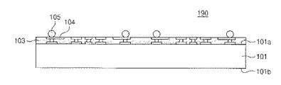
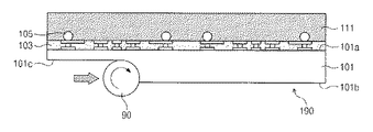
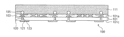
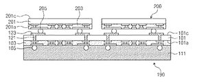
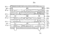
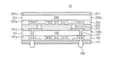
図1A乃至図1Jは本発明の一実施形態による半導体パッケージの製造方法を示した断面図である。図1Dは図1Bの変形形態を示した断面図である。
図1Aを参照すれば、ウエハー101上に活性層が形成されたウエハーレベルチップ190が提供され得る。一例によれば、活性層は回路層103であり、本発明はこれに限定されない。ウエハー101は前面101aと第1後面101bとを有するシリコンのような半導体を包含することができる。ウエハーレベルチップ190の前面101aの上には回路層103と電気的に連結されたバンプ105が提供され得る。回路層103はメモリ回路、ロジック回路或いはこれらの組み合わせのような集積回路を含み、回路層103の構成要素と電気的に連結された前面パッド104をさらに包含することができる。バンプ105は前面パッド104に直接或いは間接的に接続されて回路層103と電気的に連結され得る。
図1Bを参照すれば、ウエハーレベルチップ190上に前面モールド層111を形成し、ウエハー101を薄型化することができる。例えば、ウエハー101の前面101a上に前面モールド層111を形成し、ウエハー101を研磨することができる。一例として、前面モールド層111がウエハー101を支持した状態でウエハー101の第1後面101bをグラインダ90によって研磨することができる。前記ウエハー後面研磨によってウエハー101の厚さが縮小されて第2後面101cが露出され得る。一例によれば、ウエハー101は機械的な工程のような薄型化工程によって薄型化され得る。本明細書で前面は活性面に相当し、第2後面は非活性面に相当することがあり得る。
前面モールド層111はウエハー101に剛性乃至硬直性を提供するのに充分な厚さを有するので、ウエハー後面研磨工程の時、ウエハー101は曲がらず、屈曲されず、或いは変形されず、その状態を維持することができる。以下ではウエハー101の曲げに対して説明されるが、本発明の実施形態はこれに限定されず、ウエハー101の屈曲、変形、或いは歪み等に対しても適用され得る。前面モールド層111は絶縁体、例えばエポキシ樹脂のような高分子物質を包含することができる。エポキシ樹脂は約50〜80ppm/℃の熱膨張係数CTEを有していると知られている。ウエハー101を構成するシリコンのCTEは大略3ppm/℃であるので、ウエハー101と前面モールド層111との間の熱膨張係数の差(CTEmismatch)によってウエハー101の歪み(warpage)現象が発生することがあり得る。本発明をこれに限定しようとする意図ではなく、単なる一例として、前面モールド層111はエポキシ樹脂にシリカが混合された(例:約80wt%のシリカ含量)約5〜7ppm/℃のCTEを有するエポキシピラー複合体を包含することができる。このようにウエハー101のCTEと類似のCTEを有する前面モールド層111を形成することによってウエハー101の歪み現象が無くなるか、或いは減少され得る。一例によれば、ウエハー101の熱膨張係数CTEと前面モールド層111の熱膨張係数CTEとは同じ大きさの程度(same order of magnitude)、例えば2つの熱膨張係数は1乃至10ppm/℃であり得る。他の例として、前面モールド層111の熱膨張係数CTE:ウエハー101の熱膨張係数CTE=3:1であり得る。
本実施形態によれば、前記ウエハー後面研磨工程の時、前面モールド層111がウエハー101を支持するので、ウエハー101の前面101a上に接着剤を利用してキャリヤーを付着する工程が必要としない。その上に、前面モールド層111はウエハー101と類似のCTEを有するので、歪み現象によるウエハー101の損傷を避けることができる。
前面モールド層111はウエハー101と回路層103とを含むウエハーレベルチップ190に全体的に剛性乃至硬直性を提供する。ウエハー研磨工程の時、ウエハーレベルチップ190、特に前面モールド層111は剛性乃至硬直性を提供して曲げやすいことを防止する真空チャックやその以外の他の器具のような装置によって支持される。一例として、真空チャックは前面モールド層111に直接接触して支持することができる。
前記装置は接着剤の使用無しで前面モールド層111に脱付着され得る。例えば、前記装置は前面モールド層111に接着されない状態で脱付着され得る。他の例として、前記装置と前面モールド層111との間に接着剤を形成しなかった状態で前記装置が前面モールド層111とに脱付着され得る。
図1Cを参照すれば、ウエハー101を貫通して回路層103に電気的に連結される貫通電極121を形成することができる。言い換えれば、貫通電極121は貫通シリコンビアTSVであり得る。例えば、ウエハー101の非活性面101cをドライエッチングするか、或いはドリリングして垂直ホール120を形成し、垂直ホール120をタングステンや銅等のような伝導体を電気鍍金するか、或いは蒸着して貫通電極121を形成することができる。ウエハー101の非活性面101c上に貫通電極121と連結される後面パッド123をさらに形成することができる。一例として、電気鍍金で貫通電極121と後面パッド123とを同時に形成することができる。この場合、貫通電極121と後面パッド123とは一体化された1つの構造(single structure)を成し得る。他の例として、貫通電極121を形成した後に後面パッド123を別個の工程で形成することができる。
他の例として、図1Dに示したように、ウエハー101はウエハー101を一部貫通して第1後面101bに至らない貫通電極121を包含することができる。ウエハー101の前面101a上に前面モールド層111を形成し、ウエハー101は、前面モールド層111がウエハー101を支持する状態で、グラインダ90で第1後面101bを研磨することができる。前記ウエハー後面研磨は貫通電極121を露出させる第2後面101cが露出される時まで進行することができる。続いて、ウエハー101の第2後面101c上に貫通電極121と連結される図1Cに図示されたような後面パッド123を形成することができる。
本実施形態によれば、貫通電極121は図1Cに図示したようにウエハー後面研磨後に即ち、ビアラスト(Via Last)工程で形成するか、又は図1Dに示したようにウエハー後面研磨以前に、即ちビアファースト(Via First)或いはビアミドル(Via Middle)工程で形成され得る。このように本実施形態はビアファースト、ビアミドル、ビアラスト工程の全てに適用され得る。
図1Eを参照すれば、ウエハーレベルチップ190上に複数個のチップ200を積層することができる。例えば、基板201の活性面201aがウエハー101の非活性面101cに向かうようにチップ200を覆してフリップチップ実装することができる。ウエハー101は非活性面101cが上に向かうように覆してあり得る。チップ200は基板201の活性面201a上に提供された回路層203に電気的に連結されたバンプ205が貫通電極121に連結されることによってウエハー101の回路層103と電気的に連結され得る。チップ200の回路層203はメモリ回路、ロジック回路、或いはこれらの組み合わせを包含することができる。基板201はチップ単位の半導体ウエハーであり得る。チップ200のバンプ205は貫通電極121と垂直整列されるか、或いは垂直整列されないことがあり得る。垂直整列されないバンプ205と貫通電極121とを電気的に連結するために後面パッド123は再配線されてあり得る。
図1Fを参照すれば、ウエハー101の非活性面101c上にチップ200をモールディングする後面モールド層211を形成し、前面モールド層111を除去することができる。一例として、後面モールド層211はウエハー101を含む最終構造に剛性を提供することができる。後面モールド層211は前面モールド層111と同一又は類似のエポキシピラー複合体を包含することができる。前面モールド層111はグラインディング工程、化学機械的な研磨工程、或いはエッチング工程で除去することができる。例えば、滑らかで平坦な面が形成され得る。一例によれば、前面モールド層111はバンプ105が露出される時までグラインダ90によって研磨され得る。これにしたがって、ウエハー101の活性面101a乃至回路層103は隣接するバンプ105の間を満たす前面モールド層111で覆われていることがあり得る。図1Bを参照して前述したように、前面モールド層111が研磨される時、真空チャックやその以外の他の器具のような装置が前面モールド層111に脱付着される方法と類似に後面モールド層211に脱付着され得る。一例として、真空チャックは後面モールド層211に直接接触して支持(hold)することができる。
図1Gを参照すれば、バンプ105上に第2バンプ107を付着して外部端子109を形成することができる。第2バンプ107は蒸発(evaporation)、電気鍍金(electrolytic plating)、無電解鍍金(electroless plating)、ボールドロップ(ball drop)、スクリーンプリンティング(screen printing)工程等にバンプ105上にソルダペースト等を提供した後、リフロして形成することができる。前記一連の工程を通じてウエハーレベルチップ190上に複数個のチップ200が積層されたウエハーレベルパッケージ1を製造することができる。ウエハーレベルパッケージ1は以下で後述するようにパッケージングされ得る。
図1Hを参照すれば、ウエハーレベルパッケージ1をダイシングすることができる。一例として、ブレード95やレーザーを利用して隣接するチップ200間の後面モールド層211、ウエハー101、前面モールド層111を分離することができる。前記ダイシングによってウエハーレベルチップ190は複数個に単位チップ、例えば図1Iのチップ100に分離され得る。
図1Iを参照すれば、前記ダイシングによってウエハーレベルパッケージ1が分離されて、チップ100(以下、マスターチップ)上にチップ200(以下、スレーブチップ)が積層された複数個のチップレベルの半導体パッケージ11が製造され得る。マスターチップ100はスレーブチップ200に比べて左右幅が大きい大きさを有することができる。マスターチップ100はウエハー101のダイシングによって形成されるので、マスターチップ100の側面100sは露出され得る。反面に、スレーブチップ200は後面モールド層211にモールディングされており、その側面200sは露出されないこともあり得る。前面モールド層111はマスターチップ100の回路層103を覆う保護層として活用され得る。一例として、前面モールド層111の幅と後面モールド層211の幅との中でいずれか1つ、そしてウエハーレベルパッケージ1のカッティングされたウエハー101の幅はスレーブチップ200の幅に比べて実質的に大きくなり得る。他の例として、前面モールド層111の幅、後面モールド層211の幅、及びウエハーレベルパッケージ1のカッティングされたウエハー101の幅は実質的に同一であり得る。
本実施形態によれば、半導体パッケージ11はマスターチップ100の非活性面101cとスレーブチップ200の活性面201aが対面する方式に積層されたバック−フロント(back−to−front)構造を有することができる。スレーブチップ200のバンプ205がマスターチップ100の貫通電極121と連結されることによって、スレーブチップ200とマスターチップ100とが電気的に連結され得る。外部端子109は前面モールド層111上へ突出されることによって、半導体パッケージ11と電気的な装置(例:半導体チップ、半導体パッケージ、印刷回路基板、モジュール基板)との電気的な連結が容易になり得る。一例として、後面モールド層211はスレーブチップ200とカッティングされたウエハー101との間に配置されないことがあり得る。
図1Jを参照すれば、半導体パッケージ11をパッケージ基板80上に実装して半導体パッケージ12を製造することができる。一例として、印刷回路基板のようなパッケージ基板80の前面80a上に半導体パッケージ11を実装し、半導体パッケージ11を覆う外部モールド層83を形成して半導体パッケージ12を製造することができる。パッケージ基板80の後面80bにソルダボール85を付着することができる。マスターチップ100は前面モールド層111と、後面モールド層211と、外部モールド層83とによって囲まれてモールディングされ得る。スレーブチップ200は後面モールド層211と外部モールド層83とによって二重に囲まれてモールディングされ得る。半導体パッケージ12は外部端子109を媒介にパッケージ基板80と電気的に連結され、ソルダボール85を通じて電気的な装置(例:半導体チップ、半導体パッケージ、モジュール基板)と電気的に連結され得る。
<実施形態2>
図2A乃至図2Dは本発明の他の実施形態による半導体パッケージの製造方法を示した断面図である。以下には第1実施形態と異なる点に対して詳説し、同一な点に対しては省略するか、或いは概説する。
図2Aを参照すれば、ウエハーレベルチップ190上に複数個のチップ200を積層し、前面モールド層111を除去することができる。一例として、図1A乃至図1Fで説明したことと同一又は類似にウエハー101の活性面101a上に前面モールド層111を形成した後、ウエハー101を研磨し、貫通電極121と後面パッド123とを形成した後、ウエハー101の非活性面101c上に複数個のチップ200をフリップチップ実装し、ウエハー101の非活性面101c上にチップ200をモールディングする後面モールド層211を形成した後、前面モールド層111を除去することができる。一例によれば、前面モールド層111を選択的に除去することができる化学物質を提供して前面モールド層111を除去することができる。
図2Bを参照すれば、前面モールド層111の除去によってウエハー101の非活性面101c上に複数個のチップ200がフリップチップ実装されたウエハーレベルパッケージ2が製造され得る。本実施形態によれば、前面モールド層111が完全に除去されて、バンプ105は突出された状態を有することができる。他の例として、前面モールド層111は完全に除去されなく、バンプ105を埋め込まらせない厚さにウエハー101の活性面101a乃至回路層103上に残留することができる。
図2Cを参照すれば、ウエハーレベルパッケージ2をダイシングして半導体パッケージ21を製造することができる。半導体パッケージ21はマスターチップ100上にスレーブチップ200がフリップチップ実装されたバック−フロント構造を有することができる。本実施形態によれば、バンプ105が突出されているので、バンプ105上に第2バンプを形成する工程が必要としないことがあり得る。
図2Dを参照すれば、半導体パッケージ21を印刷回路基板のようなパッケージ基板80の前面80a上に実装し、外部モールド層83を形成して半導体パッケージ22を製造することができる。マスターチップ100は後面モールド層211と外部モールド層83とによって囲まれてモールディングされ得る。スレーブチップ200は後面モールド層211と外部モールド層83とによって二重に囲まれてモールディングされ得る。
<実施形態3>
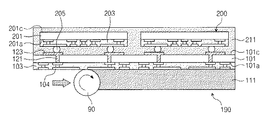
図3A乃至図3Hは本発明のその他の実施形態による半導体パッケージの製造方法を示した断面図である。図3Iは図3Aの変形形態を示した断面図である。図3Jは図3Gの変形形態を示した断面図である。
以下には第1実施形態と異なる点に対して詳説し、同一な点に対しては省略するか、或いは概説する。
図3Aを参照すれば、ウエハーレベルチップ190上に複数個のチップ200を積層することができる。例えば、図1A乃至図1Eで説明したことと同一又は類似にウエハー101の活性面101a上に前面モールド層111を形成した後、ウエハー101を研磨し、そして貫通電極121と後面パッド123とを形成した後、ウエハー101の非活性面101c上に複数個のチップ200を実装することができる。チップ200は前面201aと第1後面201bとを有する基板201上に提供された回路層203とバンプ205とを包含することができる。チップ200はウエハー101の非活性面101c上にフリップチップが実装され、バンプ205と貫通電極121とが連結されてウエハー101の回路層103と電気的に連結され得る。
図3Bを参照すれば、ウエハーレベルチップ190上に後面モールド層211を形成し、チップ200を薄型化することができる。一例として、ウエハー101の非活性面101c上にチップ200をモールディングする後面モールド層211を形成し、チップ200を研磨することができる。後面モールド層211はチップ200の第1後面201bを覆う形態であるか、或いは露出させる形態を有することができる。チップ200を練磨することはグラインダ90を利用するグラインディング工程或いは化学機械的な研磨工程を包含することができる。前記チップ研磨によってチップ200の第1後面201bが練磨されて第2後面201b(以下、非活性面)が露出され得る。後面モールド層211はチップ200と共に練磨されてチップ200をモールディングし、チップ200の非活性面201cを露出させる形態を有することができる。言い換えれば、後面モールド層211はチップ200の間、及びチップ200とウエハー101との間を満たすことができる。
図3Cを参照すれば、チップ200の基板201を貫通して回路層203と電気的に連結される貫通電極221を形成することができる。例えば、チップ200の非活性面201cをドライエッチングするか、或いはドリリングして垂直ホール220を形成し、垂直ホール220をタングステンや銅等のような伝導体を電気鍍金するか、或いは蒸着して貫通電極221を形成することができる。チップ200の非活性面201c上に貫通電極221と連結される後面パッド223をさらに形成することができる。一例として、電気鍍金によって貫通電極221と後面パッド223とを同時に蒸着して一体化された1つの構造に形成することができる。他の例として、貫通電極221を形成した後に後面パッド223を別個の工程によって形成することができる。その他の例として、図1Dに図示されたことと類似に、チップ200はビアファースト或いはビアミドル工程によって形成された貫通電極221を包含することができる。この場合、前記チップ研磨によって貫通電極221を露出させた後、貫通電極221と連結される後面パッド223を形成することができる。
図3Dを参照すれば、チップ200の非活性面201c上に複数個のチップ300を実装することができる。チップ200(以下、第1スレーブチップ)とチップ300(以下、第2スレーブチップ)は1:1対応され得る。第2スレーブチップ300は活性面301aと非活性面301cとを有する基板301上に提供された回路層303とバンプ305とを包含することができる。第2スレーブチップ300は第1スレーブチップ200の非活性面201c上にフリップチップ実装され、バンプ305と貫通電極221とが連結されることによって第1スレーブチップ200と電気的に連結され得る。第2スレーブチップ300の回路層303はメモリ回路、ロジック回路、或いはこれらの組み合わせを包含することができる。第2スレーブチップ300の基板301はチップ単位の半導体ウエハーであり得る。
図3Eを参照すれば、第2スレーブチップ300をモールディングする第2後面モールド層311を形成し、前面モールド層111を除去することができる。一例によれば、グラインダ90で前面モールド層111を研磨してバンプ105を露出させ得る。前面モールド層111は一部が残留して隣接するバンプ105間を満たすことができる。他の例として、前面モールド層111は図2A及び図2Bに示したように化学物質を利用するエッチングによって完全に除去されるか、或いはバンプ105を露出させる埋め込まさせない厚さにウエハー101の活性面101a上に残留することができる。
図3Fを参照すれば、バンプ105上に第2バンプ107を付着して外部端子109を形成することによってウエハーレベルパッケージ3を製造することができる。ウエハーレベルパッケージ3はウエハーレベルチップ190上にフリップチップ実装された第1スレーブチップ200と第2スレーブチップ300とを包含することができる。
図3Gを参照すれば、ウエハーレベルパッケージ3をダイシングしてウエハー101が分離されて形成されたマスターチップ100上に第1スレーブチップ200と第2スレーブチップ300とがフリップチップ実装された半導体パッケージ31を製造することができる。半導体パッケージ31はマスターチップ100と第1スレーブチップ200との間のバック−フロント構造及び第1スレーブチップ200と第2スレーブチップ300との間のバック−フロント構造を有することができる。第1スレーブチップ200のバンプ205がマスターチップ100の貫通電極121と連結されることによって、第1スレーブチップ200とマスターチップ100とが電気的に連結され、第2スレーブチップ300のバンプ305が第1スレーブチップ200の貫通電極221と連結されることによって、第1スレーブチップ200と第2スレーブチップ300とが電気的に連結され得る。
マスターチップ100は第1スレーブチップ200と第2スレーブチップ300とに比べて左右幅が大きい大きさを有することができる。第2スレーブチップ200と第2スレーブチップ300とは同一であるか、或いは類似の幅を有することができる。マスターチップ100はウエハー101のダイシングによって形成されるので、マスターチップ100の側面100sは露出され得る。反面に、第1スレーブチップ200の側面200sは後面モールド層211によって覆っており、第2スレーブチップ300の側面300sは第2後面モールド層311によって覆っているので、露出されないこともあり得る。
図3Hを参照すれば、半導体パッケージ31を印刷回路基板のようなパッケージ基板80の前面80a上に実装し、外部モールド層83を形成して半導体パッケージ32を製造することができる。マスターチップ100は前面モールド層111と、後面モールド層211と、外部モールド層83とによって囲まれてモールディングされ得る。第1スレーブチップ200は第1スレーブチップ200を囲む後面モールド層211及び第2後面モールド層311を外部モールド層83がさらに囲む形態にモールディングされ得る。第2スレーブチップ300は第2後面モールド層311と外部モールド層83とによって二重に囲まれてモールディングされ得る。
他の例として、図3Iに示したようにウエハーレベルチップ190上に上部ウエハーレベルチップ290を積層することができる。上部ウエハーレベルチップ290は回路層203とバンプ205が提供された上部ウエハー201を包含することができる。上部ウエハー201はその活性面201aがウエハー101の非活性面101cに向かうように覆して下部ウエハー101上に積層され得る。上部ウエハー201の第1後面201bが図3Bでのように練磨されて非活性面201cが露出され得る。
図3B乃至図3Gで説明したことと同一又は類似の工程によってマスターチップ100上に第1スレーブチップ200と第2スレーブチップ300とがフリップチップ実装された半導体パッケージ31aが製造され得る。マスターチップ100はウエハー101のダイシングによって形成されるので、その側面100sが露出され得る。類似に、第1スレーブチップ200は上部ウエハー201のダイシングによって形成されるので、その側面200sが露出され得る。反面に、第2スレーブチップ300の側面300sは第2後面モールド層311によって覆っているので、露出されないこともあり得る。半導体パッケージ31aはパッケージ基板80上に実装され、外部モールド層83によってモールディングされて図3Hに図示された半導体パッケージ32と類似にパッケージングされ得る。
<実施形態4>
図4A乃至図4Eは本発明のその他の実施形態による半導体パッケージの製造方法を示した断面図である。以下には第1実施形態と異なる点に対して詳説し、同一な点に対しては省略するか、或いは概説する。
図4Aを参照すれば、ウエハーレベルチップ190上に複数個の半導体パッケージ11を積層することができる。一例として、図1A乃至図1Cで説明したことと同一又は類似にウエハー101の活性面101a上に前面モールド層111を形成し、ウエハー101を研磨した後、貫通電極121と後面パッド123とを形成することができる。その後、ウエハー101の非活性面101c上に図1Iに図示された複数個の半導体パッケージ11を実装することができる。半導体パッケージ11の外部端子109がウエハーレベルチップ190の貫通電極121に連結されることによって、半導体パッケージ1とウエハーレベルチップ190とが電気的に連結され得る。
図4Bを参照すれば、ウエハー101の非活性面101c上に半導体パッケージ11をモールディングする後面モールド層211を形成し、前面モールド層111を除去することができる。前面モールド層111はグラインダ90を利用するグラインディング工程、或いは化学物質を利用するエッチング工程等に除去されることができる。例えばグラインダ90で前面モールド層111を研磨してバンプ105を露出させ得る。
図4Cを参照すれば、バンプ105上に第2バンプ107を付着して外部端子109aを形成することによってウエハーレベルパッケージ4を製造することができる。ウエハーレベルパッケージ4はウエハーレベルチップ190上に実装された複数個の半導体パッケージ11を包含することができる。
図4Dを参照すれば、ウエハーレベルパッケージ4をダイシングしてウエハー101が分離されて形成されたマスターチップ100上に半導体パッケージ11が実装された半導体パッケージ41を製造することができる。一例によれば、マスターチップ100の側面100sは露出され、半導体パッケージ11は後面モールド層211によってモールディングされ得る。
図4Eを参照すれば、半導体パッケージ41を印刷回路基板のようなパッケージ基板80の前面80a上に実装し、外部モールド層83を形成して、半導体パッケージ42を製造することができる。マスターチップ100は前面モールド層111と、後面モールド層211と、外部モールド層83とによって囲まれてモールディングされ得る。半導体パッケージ11は後面モールド層111と外部モールド層83とによって二重に囲まれてモールディングされ得る。
<実施形態5>
図5A乃至図5Eは本発明のその他の実施形態による半導体パッケージの製造方法を示した断面図である。以下には第1実施形態と異なる点に対して詳説し、同一な点に対しては省略するか、或いは概説する。
図5Aを参照すれば、下部ウエハーレベルチップ190上に上部ウエハーレベルチップ295を積層することができる。例えば、図1A乃至図1Cで説明したことと同一又は類似にウエハー101の活性面101a上に前面モールド層111を形成し、ウエハー101を研磨した後、貫通電極121と後面パッド123とを形成することができる。その後、ウエハー101(以下、下部ウエハー)の非活性面101c上に回路層253を有するウエハー251(以下、上部ウエハー)を積層することができる。上部ウエハー251は活性面251aと非活性面251cとを有するシリコンのような半導体を包含することができる。上部ウエハー251の活性面251aの上には回路層253と電気的に連結されたバンプ255が提供され得る。上部ウエハー251はその活性面251aが下部ウエハー101の非活性面101cに向かうように覆して下部ウエハー101上に積層され得る。
図5Bを参照すれば、下部ウエハー101の非活性面101c上に上部ウエハーレベルチップ295をモールディングする後面モールド層211を形成し、前面モールド層111を除去することができる。前面モールド層111はグラインダ90によってバンプ105を露出させる時まで研磨され得る。他の例として、前面モールド層111は図2A及び図2Bに示したように化学物質を利用するエッチングによって完全に除去されるか、或いはバンプ105を露出させる埋め込まさせない厚さにウエハー101の活性面101a上に残留することができる。
図5Cを参照すれば、バンプ105上に第2バンプ107を付着して外部端子109を形成することができる。前記一連の工程を通じて上部ウエハーレベルチップ295が後面モールド層211でモールディングされて、下部ウエハーレベルチップ190上に積層されたウエハーレベルパッケージ5を製造することができる。
図5Dを参照すれば、ウエハーレベルパッケージ5をダイシングして下部ウエハー101が分離されて形成されたマスターチップ100上に上部ウエハー251が分離されて形成されたスレーブチップ250が実装された半導体パッケージ51を製造することができる。マスターチップ100の側面100sとスレーブチップ250の側面250sとは露出され得る。
図5Eを参照すれば、半導体パッケージ51を印刷回路基板のようなパッケージ基板80の前面80a上に実装し、外部モールド層83を形成して、半導体パッケージ52を製造することができる。マスターチップ100は前面モールド層111と、後面モールド層211と、外部モールド層83とによって囲まれてモールディングされ得る。スレーブチップ250は後面モールド層211と外部モールド層83とによって囲まれてモールディングされ得る。
<実施形態6>
図6A乃至図6Dは本発明のその他の実施形態による半導体パッケージの製造方法を示した断面図である。以下には第1実施形態と異なる点に対して詳説し、同一な点に対しては省略するか、或いは概説する。
図6Aを参照すれば、ウエハーレベルチップ190上に複数個のチップ200を積層することができる。例えば、図1A乃至図1Eで説明したことと同一又は類似にウエハー101の活性面101a上に前面モールド層111を形成し、ウエハー101を研磨した後、貫通電極121と後面パッド123とを形成し、そしてウエハー101の非活性面101c上に複数個のチップ200をフリップチップ実装することができる。本実施形態によれば、ウエハーレベルチップ190はウエハー101の活性面101a上に提供されて前面パッド104と連結されるバンプを包含しないことがあり得る。
図6Bを参照すれば、ウエハーレベルチップ190上に後面モールド層211を形成し、前面モールド層111をグラインディング工程、化学機械的研磨工程、或いはエッチング工程等によって除去することができる。一例によれば、前面モールド層111はグラインダ90によって練磨されて前面パッド104が露出され得る。
図6Cを参照すれば、前面モールド層111の除去によってウエハーレベルチップ190上に複数個のチップ200が積層されたウエハーレベルパッケージ6が製造され得る。バンプ205が貫通電極121と連結されることによって、チップ200がウエハーレベルチップ190と電気的に連結され得る。
図6Dを参照すれば、ウエハーレベルパッケージ6のダイシングによって形成されたチップ積層体195を印刷回路基板のようなパッケージ基板70上に実装して半導体パッケージ61を製造することができる。一例として、前面パッド104に連結されるボンディングパッド74を形成し、接着層71の介在下にチップ積層体195を実装してパッケージ基板70の前面70a上に実装することができる。チップ積層体195はウエハー101のダイシングによって分離されて形成されたマスターチップ100上にフリップチップ実装されたスレーブチップ200を包含することができる。
パッケージ基板70の後面70bにはソルダボール75が付着され得る。本実施形態によれば、パッケージ基板70はチップ積層体195のセンターを開放するウインドー70wを包含することができる。チップ積層体195はウインドー70wを通過してボンディングパッド74に接続するボンディングワイヤ72を通じてパッケージ基板70と電気的に連結され得る。ウインドー70wはボンディングワイヤ72を固定させ、保護するモールド層73によって満たされ得る。
<応用例>
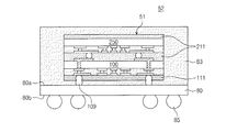
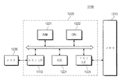
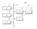
図7Aは本発明の実施形態による半導体パッケージを具備するメモリカードを示したブロック図である。図7Bは本発明の実施形態による半導体パッケージを応用した情報処理システムを示したブロック図である。
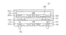
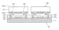
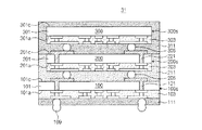
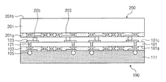
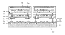
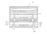
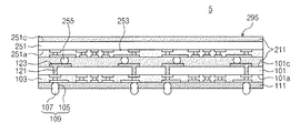
図7Aを参照すれば、メモリカード1200はホストとメモリ1210との間の諸般データ交換を制御するメモリコントローラ1220を包含することができる。SRAM1221は中央処理装置1222の動作メモリとして使用され得る。ホストインターフェイス1223はメモリカード1200と接続されるホストのデータ交換プロトコルを具備することができる。誤謬修正コード1224はメモリ1210から読出されたデータに含まれる誤謬を検出及び訂正することができる。メモリインターフェイス1225はメモリ1210とインターフェイシングする。中央処理装置1222はメモリコントローラ1220のデータを交換するための諸般制御動作を遂行することができる。メモリ1210は本実施形態の半導体パッケージの中で少なくともいずれか1つを包含することができる。
図7Bを参照すれば、情報処理システム1300は本実施形態の半導体パッケージの中で少なくともいずれか1つを具備するメモリシステム1310を包含することができる。情報処理システム1300はモバイル機器やコンピューター等を包含することができる。一例として、情報処理システム1300はシステムバス1360に電気的に連結されたメモリシステム1310、モデム1320、中央処理装置1330、RAM1340、ユーザーインターフェイス1350を包含することができる。メモリシステム1310はメモリ1311とメモリコントローラ1312とを包含でき、図7Aのメモリカード1200と実質的に同様に構成され得る。このようなメモリシステム1310には中央処理装置1330によって処理されたデータ又は外部から入力されたデータが格納され得る。情報処理システム1300はメモリカード、半導体ディスク装置(Solid State Disk)、カメライメージプロセッサ(Camera Image Sensor)、及びその他の応用チップセット(Application Chipset)に提供され得る。
以上の発明の詳細な説明は開示された実施状態に本発明を制限しようとする意図ではなく、本発明の要旨を逸脱しない範囲内で多様な他の組み合わせ、変更及び環境で使用することができる。添付された請求の範囲は他の実施状態も含むことと理解しなければならない。
1、11・・・半導体パッケージ
100・・・マスターチップ
101・・・下部ウエハー
101a・・・前面、活性面
101b・・・第1後面、非活性面
101c・・・第2後面
103・・・回路層
104・・・前面パッド
105・・・バンプ
109・・・外部端子
111・・・前面モールド層
120・・・垂直ホール
121・・・貫通電極
123・・・後面パッド
200・・・スレーブチップ

Claims (20)

  1. ウエハーの前面上に第1活性層を含む基板を提供し、
    前記第1活性層上にポリマー物質を含む第1モールド層を形成して前記基板に剛性を提供し、
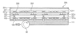
    前記第1モールド層を形成した後に、接着剤の使用無しで前記第1モールド層に装置を付着して前記基板が支持された状態で、前記基板の第1後面を除去して前記基板を薄型化し、第2後面を露出させ、
    前記薄型化された基板に前記基板に提供された貫通電極と電気的に連結されるパッドを形成することを含み、
    前記第1モールド層は、前記基板が薄型化の間に曲がらないように、基板に剛性を提供するための所定の厚さを有する、半導体素子の製造方法。
  2. 前記装置は、前記装置が前記第1モールド層に接着されないまま、前記第1モールド層に付着される請求項1に記載の半導体素子の製造方法。
  3. 前記装置は、前記装置と前記第1モールド層との間に接着剤を使用せずに、前記第1モールド層に付着される請求項1に記載の半導体素子の製造方法。
  4. 前記基板の第1後面を薄型化することは、
    機械的な工程を使用して前記第1後面を除去することを含む請求項1に記載の半導体素子の製造方法。
  5. 前記基板の第1後面を薄型化することは、
    前記基板の第1後面をグラインディングすることを含む請求項1に記載の半導体素子の製造方法。
  6. 前記薄型化された基板内に前記貫通電極を形成することをさらに含む請求項4に記載の半導体素子の製造方法。
  7. 前記薄型化された基板の第2後面上にチップを積層することをさらに含み、
    前記チップの活性面は、前記薄型化された基板の第2後面に向かう請求項6に記載の半導体素子の製造方法。
  8. 前記チップ上に前記チップをモールディングする第2モールド層を形成して前記基板に剛性を付し、
    前記第2モールド層を形成した後に前記第1モールド層の少なくとも一部を除去して滑らかで平坦な面を形成することをさらに含む請求項7に記載の半導体素子の製造方法。
  9. 前記第1及び第2モールド層と前記基板とをカッティングして半導体パッケージを形成することをさらに含み、
    前記半導体パッケージの第1モールド層の幅、前記半導体パッケージの第2モールド層の幅、及び前記半導体パッケージの基板の幅の中でいずれか1つは、前記チップの幅に比べて大きい請求項8に記載の半導体素子の製造方法。
  10. 前記半導体パッケージの第1モールド層の幅、前記半導体パッケージの第2モールド層の幅、及び前記半導体パッケージの基板の幅は、同一である請求項9に記載の半導体素子の製造方法。
  11. 前記第2モールド層は、前記チップと前記基板との間に配置されない請求項9に記載の半導体素子の製造方法。
  12. 前記基板を薄型化する時、前記装置は、前記第1モールド層と直接接触して支持する真空チャックである請求項1に記載の半導体素子の製造方法。
  13. 前記第1モールド層の少なくとも一部を除去する時、前記第2モールド層は、真空チャックに直接接触して支持される請求項8に記載の半導体素子の製造方法。
  14. 前記第1モールド層の熱膨張係数CTEと前記基板の熱膨張係数CTEとは、1つの桁程度(an order of magnitude)の範囲である請求項1に記載の半導体素子の製造方法。
  15. 前記第1モールド層の熱膨張係数CTEと前記基板の熱膨張係数CTEとの比は、3乃至1である請求項1に記載の半導体素子の製造方法。
  16. 前記第1活性層は、回路層である請求項1に記載の半導体素子の製造方法。
  17. ウエハーの前面上に提供された第1活性層を含む基板を提供し、
    前記第1活性層上にポリマー物質を含む第1モールド層を形成して前記基板に剛性を付し、
    前記第1モールド層を形成した後に、前記基板の第1後面を除去して前記基板を薄型化し、第2後面を露出させ、
    前記薄型化された基板内に前記第1活性層と電気的に連結される貫通電極を形成し、
    前記薄型化された基板上に前記基板内に提供された前記貫通電極と電気的に連結されるパッドを形成することを
    み、
    前記第1モールド層の熱膨張係数CTEと前記基板の熱膨張係数CTEとは、1つの桁程度(an order of magnitude)の範囲である、半導体素子の製造方法。
  18. 前記第1モールド層は、装置が前記第1モールド層に接着されないまま、前記装置に付着される、請求項17に記載の半導体素子の製造方法。
  19. 前記第1モールド層は、装置と前記第1モールド層との間に接着剤を使用せずに、前記装置に付着される、請求項17に記載の半導体素子の製造方法。
  20. 前面上に第1活性層を含む基板を提供し、
    前記第1活性層上に第1モールド層を形成して前記基板に剛性を提供し、
    前記第1モールド層を形成した後に、前記基板の第1後面を除去して前記基板を薄型化し、第2後面を露出させ、
    前記薄型化された基板内に前記第1活性層と電気的に連結される貫通電極を形成し、
    前記薄型化された基板に前記基板内に提供された前記貫通電極と電気的に連結されるパッドを形成し、
    前記薄型化された基板の第2後面上に、チップの活性面が前記薄型化された基板の第2後面に向かう前記チップを積層すること含み、
    前記基板が薄型化されるときに接着剤の使用無しで装置に前記第1モールド層を付着して、前記基板が支持され、
    前記第1モールド層の幅、及び前記基板の幅は、同一である、半導体素子の製造方法。
JP2014125069A 2013-06-21 2014-06-18 貫通電極を有する半導体パッケージ及びその製造方法 Active JP5908030B2 (ja)

Applications Claiming Priority (4)

Application Number Priority Date Filing Date Title
KR10-2013-0071775 2013-06-21
KR1020130071775A KR102077153B1 (ko) 2013-06-21 2013-06-21 관통전극을 갖는 반도체 패키지 및 그 제조방법
US14/264,120 US9245771B2 (en) 2013-06-21 2014-04-29 Semiconductor packages having through electrodes and methods for fabricating the same
US14/264,120 2014-04-29

Publications (3)

Publication Number Publication Date
JP2015005748A JP2015005748A (ja) 2015-01-08
JP2015005748A5 JP2015005748A5 (ja) 2016-02-25
JP5908030B2 true JP5908030B2 (ja) 2016-04-26

Family

ID=52111252

Family Applications (1)

Application Number Title Priority Date Filing Date
JP2014125069A Active JP5908030B2 (ja) 2013-06-21 2014-06-18 貫通電極を有する半導体パッケージ及びその製造方法

Country Status (4)

Country Link
US (1) US9245771B2 (ja)
JP (1) JP5908030B2 (ja)
KR (1) KR102077153B1 (ja)
CN (1) CN104241229B (ja)

Families Citing this family (25)

* Cited by examiner, † Cited by third party
Publication number Priority date Publication date Assignee Title
KR102174336B1 (ko) * 2014-07-08 2020-11-04 삼성전자주식회사 반도체 패키지 및 그 제조 방법
US9899285B2 (en) * 2015-07-30 2018-02-20 Semtech Corporation Semiconductor device and method of forming small Z semiconductor package
US20170062240A1 (en) * 2015-08-25 2017-03-02 Inotera Memories, Inc. Method for manufacturing a wafer level package
JP2017073472A (ja) * 2015-10-07 2017-04-13 株式会社ディスコ 半導体装置の製造方法
US10872879B2 (en) 2015-11-12 2020-12-22 Amkor Technology Singapore Holding Pte. Ltd. Semiconductor package and manufacturing method thereof
KR101712288B1 (ko) * 2015-11-12 2017-03-03 앰코 테크놀로지 코리아 주식회사 반도체 패키지 및 그 제조 방법
KR102506697B1 (ko) * 2016-05-18 2023-03-08 에스케이하이닉스 주식회사 관통 몰드 볼 커넥터를 포함하는 반도체 패키지
US10204893B2 (en) 2016-05-19 2019-02-12 Invensas Bonding Technologies, Inc. Stacked dies and methods for forming bonded structures
US9922845B1 (en) * 2016-11-03 2018-03-20 Micron Technology, Inc. Semiconductor package and fabrication method thereof
US10879212B2 (en) 2017-05-11 2020-12-29 Invensas Bonding Technologies, Inc. Processed stacked dies
US20180358398A1 (en) * 2017-06-13 2018-12-13 Xintec Inc. Chip package and manufacturing method thereof
KR102085654B1 (ko) * 2017-12-07 2020-03-06 주식회사 아모텍 다이오드 복합소자 및 그의 제조 방법
US11276676B2 (en) 2018-05-15 2022-03-15 Invensas Bonding Technologies, Inc. Stacked devices and methods of fabrication
US10727204B2 (en) * 2018-05-29 2020-07-28 Advances Micro Devices, Inc. Die stacking for multi-tier 3D integration
US11158606B2 (en) 2018-07-06 2021-10-26 Invensas Bonding Technologies, Inc. Molded direct bonded and interconnected stack
CN108831861A (zh) * 2018-08-09 2018-11-16 苏州晶方半导体科技股份有限公司 堆叠式芯片封装方法及封装结构
US20220406765A9 (en) * 2018-10-02 2022-12-22 Micron Technology, Inc. Semiconductor device packages having stacked semiconductor dice
WO2020085715A1 (ko) * 2018-10-26 2020-04-30 주식회사 네패스 반도체 패키지
CN113330557A (zh) 2019-01-14 2021-08-31 伊文萨思粘合技术公司 键合结构
US11296053B2 (en) 2019-06-26 2022-04-05 Invensas Bonding Technologies, Inc. Direct bonded stack structures for increased reliability and improved yield in microelectronics
KR20210013429A (ko) 2019-07-25 2021-02-04 삼성전자주식회사 반도체 패키지 및 그의 제조 방법
JP7488116B2 (ja) 2020-06-03 2024-05-21 株式会社ディスコ 電極形成方法
KR20220009218A (ko) 2020-07-15 2022-01-24 삼성전자주식회사 반도체 패키지, 및 이를 가지는 패키지 온 패키지
US20220165669A1 (en) * 2020-11-25 2022-05-26 Taiwan Semiconductor Manufacturing Company, Ltd. Semiconductor device structure, stacked semiconductor device structure and method of manufacturing semiconductor device structure
CN113035825A (zh) * 2021-02-02 2021-06-25 日月光半导体制造股份有限公司 半导体封装结构及其形成方法

Family Cites Families (26)

* Cited by examiner, † Cited by third party
Publication number Priority date Publication date Assignee Title
JP3525808B2 (ja) 1999-06-28 2004-05-10 松下電器産業株式会社 半導体装置の製造方法および半導体装置
JP2001237205A (ja) * 2000-02-24 2001-08-31 Sumitomo Metal Ind Ltd 化学機械的研磨装置、ダマシン配線形成装置及びダマシン配線形成方法
US6841883B1 (en) * 2003-03-31 2005-01-11 Micron Technology, Inc. Multi-dice chip scale semiconductor components and wafer level methods of fabrication
JP4390775B2 (ja) 2006-02-08 2009-12-24 Okiセミコンダクタ株式会社 半導体パッケージの製造方法
US8409920B2 (en) * 2007-04-23 2013-04-02 Stats Chippac Ltd. Integrated circuit package system for package stacking and method of manufacture therefor
US7948095B2 (en) 2008-02-12 2011-05-24 United Test And Assembly Center Ltd. Semiconductor package and method of making the same
US7955895B2 (en) * 2008-11-07 2011-06-07 Taiwan Semiconductor Manufacturing Co., Ltd. Structure and method for stacked wafer fabrication
US8487444B2 (en) 2009-03-06 2013-07-16 Taiwan Semiconductor Manufacturing Company, Ltd. Three-dimensional system-in-package architecture
US8531015B2 (en) 2009-03-26 2013-09-10 Stats Chippac, Ltd. Semiconductor device and method of forming a thin wafer without a carrier
KR20100109241A (ko) 2009-03-31 2010-10-08 삼성전자주식회사 칩 적층 패키지 및 그 제조방법
US8143097B2 (en) 2009-09-23 2012-03-27 Stats Chippac, Ltd. Semiconductor device and method of forming open cavity in TSV interposer to contain semiconductor die in WLCSMP
KR20110105159A (ko) 2010-03-18 2011-09-26 주식회사 하이닉스반도체 적층 반도체 패키지 및 그 형성방법
KR101667656B1 (ko) 2010-03-24 2016-10-20 삼성전자주식회사 패키지-온-패키지 형성방법
KR101142339B1 (ko) * 2010-06-17 2012-05-17 에스케이하이닉스 주식회사 반도체 칩
US8338939B2 (en) 2010-07-12 2012-12-25 Taiwan Semiconductor Manufacturing Company, Ltd. TSV formation processes using TSV-last approach
KR101678539B1 (ko) * 2010-07-21 2016-11-23 삼성전자 주식회사 적층 패키지, 반도체 패키지 및 적층 패키지의 제조 방법
KR20120045402A (ko) 2010-10-29 2012-05-09 에스케이하이닉스 주식회사 반도체 집적회로 및 그의 제조 방법
KR20120053332A (ko) 2010-11-17 2012-05-25 삼성전자주식회사 반도체 패키지 및 이의 제조 방법
JP2012209545A (ja) 2011-03-17 2012-10-25 Sekisui Chem Co Ltd 半導体積層体の製造方法
KR20120123919A (ko) 2011-05-02 2012-11-12 삼성전자주식회사 칩 적층 반도체 패키지 제조 방법 및 이에 의해 제조된 칩 적층 반도체 패키지
US8642385B2 (en) 2011-08-09 2014-02-04 Alpha & Omega Semiconductor, Inc. Wafer level package structure and the fabrication method thereof
US8853003B2 (en) * 2011-08-09 2014-10-07 Alpha & Omega Semiconductor, Inc. Wafer level chip scale package with thick bottom metal exposed and preparation method thereof
US8779599B2 (en) * 2011-11-16 2014-07-15 Taiwan Semiconductor Manufacturing Company, Ltd. Packages including active dies and dummy dies and methods for forming the same
KR101784507B1 (ko) * 2011-12-14 2017-10-12 에스케이하이닉스 주식회사 반도체 적층 패키지 및 제조 방법, 이를 포함하는 전자 시스템
US9006004B2 (en) * 2012-03-23 2015-04-14 Taiwan Semiconductor Manufacturing Company, Ltd. Probing chips during package formation
JP5399542B2 (ja) * 2012-08-08 2014-01-29 富士通株式会社 半導体装置の製造方法

Also Published As

Publication number Publication date
CN104241229B (zh) 2017-10-13
KR102077153B1 (ko) 2020-02-14
JP2015005748A (ja) 2015-01-08
US20140377909A1 (en) 2014-12-25
KR20150000064A (ko) 2015-01-02
US9245771B2 (en) 2016-01-26
CN104241229A (zh) 2014-12-24

Similar Documents

Publication Publication Date Title
JP5908030B2 (ja) 貫通電極を有する半導体パッケージ及びその製造方法
US11183493B2 (en) Semiconductor device using EMC wafer support system and fabricating method thereof
KR102094924B1 (ko) 관통전극을 갖는 반도체 패키지 및 그 제조방법
US10867897B2 (en) PoP device
US8536672B2 (en) Image sensor package and fabrication method thereof
TWI710079B (zh) 使用導線接合之混合式添加結構之可堆疊記憶體晶粒
TW201921625A (zh) 具有橫向偏移堆疊之半導體晶粒之半導體裝置
US20150069607A1 (en) Through via package
US11302675B2 (en) Semiconductor device and method for manufacturing the same
JP2013526066A (ja) 低減されたダイ歪みアッセンブリのためのパッケージ基板のためのcte補償
US8691625B2 (en) Method for making a chip package
US8785297B2 (en) Method for encapsulating electronic components on a wafer
US20180315718A1 (en) Semiconductor packages and devices
KR101958831B1 (ko) 양면 접착성 테이프, 반도체 패키지 및 그 제조 방법
US10991597B2 (en) Method of fabricating a semiconductor device using an adhesive layer
KR100577015B1 (ko) 반도체 소자의 적층 칩 패키지 및 그 제조 방법
KR20210129895A (ko) 반도체 패키지 및 반도체 패키지의 제조 방법
CN116313844A (zh) 基于面板形态的芯片封装方法和芯片封装件
JP2005340483A (ja) 半導体チップ、半導体装置、およびその製造方法
KR20080084282A (ko) 반도체 칩과 이의 제조방법 및 이를 이용한 반도체 패키지

Legal Events

Date Code Title Description
RD04 Notification of resignation of power of attorney

Free format text: JAPANESE INTERMEDIATE CODE: A7424

Effective date: 20141226

A521 Request for written amendment filed

Free format text: JAPANESE INTERMEDIATE CODE: A523

Effective date: 20160108

A621 Written request for application examination

Free format text: JAPANESE INTERMEDIATE CODE: A621

Effective date: 20160108

A871 Explanation of circumstances concerning accelerated examination

Free format text: JAPANESE INTERMEDIATE CODE: A871

Effective date: 20160108

A975 Report on accelerated examination

Free format text: JAPANESE INTERMEDIATE CODE: A971005

Effective date: 20160126

TRDD Decision of grant or rejection written
A01 Written decision to grant a patent or to grant a registration (utility model)

Free format text: JAPANESE INTERMEDIATE CODE: A01

Effective date: 20160222

A61 First payment of annual fees (during grant procedure)

Free format text: JAPANESE INTERMEDIATE CODE: A61

Effective date: 20160322

R150 Certificate of patent or registration of utility model

Ref document number: 5908030

Country of ref document: JP

Free format text: JAPANESE INTERMEDIATE CODE: R150

R250 Receipt of annual fees

Free format text: JAPANESE INTERMEDIATE CODE: R250

R250 Receipt of annual fees

Free format text: JAPANESE INTERMEDIATE CODE: R250

R250 Receipt of annual fees

Free format text: JAPANESE INTERMEDIATE CODE: R250

R250 Receipt of annual fees

Free format text: JAPANESE INTERMEDIATE CODE: R250

R250 Receipt of annual fees

Free format text: JAPANESE INTERMEDIATE CODE: R250

R250 Receipt of annual fees

Free format text: JAPANESE INTERMEDIATE CODE: R250