JP5789157B2 - Method for manufacturing semiconductor device - Google Patents
Method for manufacturing semiconductor device Download PDFInfo
- Publication number
- JP5789157B2 JP5789157B2 JP2011187729A JP2011187729A JP5789157B2 JP 5789157 B2 JP5789157 B2 JP 5789157B2 JP 2011187729 A JP2011187729 A JP 2011187729A JP 2011187729 A JP2011187729 A JP 2011187729A JP 5789157 B2 JP5789157 B2 JP 5789157B2
- Authority
- JP
- Japan
- Prior art keywords
- oxide semiconductor
- oxide
- sputtering target
- less
- sintered body
- Prior art date
- Legal status (The legal status is an assumption and is not a legal conclusion. Google has not performed a legal analysis and makes no representation as to the accuracy of the status listed.)
- Active
Links
- 239000004065 semiconductor Substances 0.000 title claims description 123
- 238000000034 method Methods 0.000 title claims description 41
- 238000004519 manufacturing process Methods 0.000 title claims description 20
- 238000005477 sputtering target Methods 0.000 claims description 84
- 238000010438 heat treatment Methods 0.000 claims description 28
- 229910052783 alkali metal Inorganic materials 0.000 claims description 20
- 150000001340 alkali metals Chemical class 0.000 claims description 20
- XLOMVQKBTHCTTD-UHFFFAOYSA-N Zinc monoxide Chemical compound [Zn]=O XLOMVQKBTHCTTD-UHFFFAOYSA-N 0.000 claims description 18
- 238000004544 sputter deposition Methods 0.000 claims description 13
- 239000001257 hydrogen Substances 0.000 claims description 12
- 229910052739 hydrogen Inorganic materials 0.000 claims description 12
- 239000011734 sodium Substances 0.000 claims description 12
- 239000011787 zinc oxide Substances 0.000 claims description 9
- UFHFLCQGNIYNRP-UHFFFAOYSA-N Hydrogen Chemical compound [H][H] UFHFLCQGNIYNRP-UHFFFAOYSA-N 0.000 claims description 7
- 239000013078 crystal Substances 0.000 claims description 7
- TWNQGVIAIRXVLR-UHFFFAOYSA-N oxo(oxoalumanyloxy)alumane Chemical compound O=[Al]O[Al]=O TWNQGVIAIRXVLR-UHFFFAOYSA-N 0.000 claims description 6
- AJNVQOSZGJRYEI-UHFFFAOYSA-N digallium;oxygen(2-) Chemical compound [O-2].[O-2].[O-2].[Ga+3].[Ga+3] AJNVQOSZGJRYEI-UHFFFAOYSA-N 0.000 claims description 5
- 229910001195 gallium oxide Inorganic materials 0.000 claims description 5
- DGAQECJNVWCQMB-PUAWFVPOSA-M Ilexoside XXIX Chemical compound C[C@@H]1CC[C@@]2(CC[C@@]3(C(=CC[C@H]4[C@]3(CC[C@@H]5[C@@]4(CC[C@@H](C5(C)C)OS(=O)(=O)[O-])C)C)[C@@H]2[C@]1(C)O)C)C(=O)O[C@H]6[C@@H]([C@H]([C@@H]([C@H](O6)CO)O)O)O.[Na+] DGAQECJNVWCQMB-PUAWFVPOSA-M 0.000 claims description 4
- 229910003437 indium oxide Inorganic materials 0.000 claims description 4
- PJXISJQVUVHSOJ-UHFFFAOYSA-N indium(iii) oxide Chemical compound [O-2].[O-2].[O-2].[In+3].[In+3] PJXISJQVUVHSOJ-UHFFFAOYSA-N 0.000 claims description 4
- 229910052708 sodium Inorganic materials 0.000 claims description 4
- XOLBLPGZBRYERU-UHFFFAOYSA-N tin dioxide Chemical compound O=[Sn]=O XOLBLPGZBRYERU-UHFFFAOYSA-N 0.000 claims description 4
- 229910001887 tin oxide Inorganic materials 0.000 claims description 4
- WHXSMMKQMYFTQS-UHFFFAOYSA-N Lithium Chemical compound [Li] WHXSMMKQMYFTQS-UHFFFAOYSA-N 0.000 claims description 3
- ZLMJMSJWJFRBEC-UHFFFAOYSA-N Potassium Chemical compound [K] ZLMJMSJWJFRBEC-UHFFFAOYSA-N 0.000 claims description 3
- 229910052744 lithium Inorganic materials 0.000 claims description 3
- 229910052700 potassium Inorganic materials 0.000 claims description 3
- 239000011591 potassium Substances 0.000 claims description 3
- 239000010410 layer Substances 0.000 description 38
- 239000012535 impurity Substances 0.000 description 30
- 239000000758 substrate Substances 0.000 description 21
- 238000001004 secondary ion mass spectrometry Methods 0.000 description 18
- 150000001875 compounds Chemical class 0.000 description 17
- IJGRMHOSHXDMSA-UHFFFAOYSA-N Atomic nitrogen Chemical compound N#N IJGRMHOSHXDMSA-UHFFFAOYSA-N 0.000 description 16
- 230000015572 biosynthetic process Effects 0.000 description 14
- 239000000463 material Substances 0.000 description 11
- QVGXLLKOCUKJST-UHFFFAOYSA-N atomic oxygen Chemical compound [O] QVGXLLKOCUKJST-UHFFFAOYSA-N 0.000 description 10
- 239000001301 oxygen Substances 0.000 description 10
- 229910052760 oxygen Inorganic materials 0.000 description 10
- 239000011701 zinc Substances 0.000 description 10
- 229910052784 alkaline earth metal Inorganic materials 0.000 description 9
- 150000001342 alkaline earth metals Chemical class 0.000 description 9
- 239000007789 gas Substances 0.000 description 9
- XKRFYHLGVUSROY-UHFFFAOYSA-N Argon Chemical compound [Ar] XKRFYHLGVUSROY-UHFFFAOYSA-N 0.000 description 8
- 239000002585 base Substances 0.000 description 8
- 229910052757 nitrogen Inorganic materials 0.000 description 8
- 239000013077 target material Substances 0.000 description 8
- 238000010304 firing Methods 0.000 description 6
- 125000004435 hydrogen atom Chemical group [H]* 0.000 description 6
- 229910052751 metal Inorganic materials 0.000 description 6
- 239000002184 metal Substances 0.000 description 6
- 150000002431 hydrogen Chemical class 0.000 description 5
- 239000011261 inert gas Substances 0.000 description 5
- XLYOFNOQVPJJNP-UHFFFAOYSA-N water Substances O XLYOFNOQVPJJNP-UHFFFAOYSA-N 0.000 description 5
- MYMOFIZGZYHOMD-UHFFFAOYSA-N Dioxygen Chemical compound O=O MYMOFIZGZYHOMD-UHFFFAOYSA-N 0.000 description 4
- 229910052786 argon Inorganic materials 0.000 description 4
- 229910001882 dioxygen Inorganic materials 0.000 description 4
- 239000011521 glass Substances 0.000 description 4
- 239000000843 powder Substances 0.000 description 4
- 229910005191 Ga 2 O 3 Inorganic materials 0.000 description 3
- 229910021417 amorphous silicon Inorganic materials 0.000 description 3
- 238000004140 cleaning Methods 0.000 description 3
- 238000005530 etching Methods 0.000 description 3
- 230000005669 field effect Effects 0.000 description 3
- 229910052733 gallium Inorganic materials 0.000 description 3
- -1 moisture Chemical class 0.000 description 3
- 229910021420 polycrystalline silicon Inorganic materials 0.000 description 3
- 229910018137 Al-Zn Inorganic materials 0.000 description 2
- 229910018573 Al—Zn Inorganic materials 0.000 description 2
- RYGMFSIKBFXOCR-UHFFFAOYSA-N Copper Chemical compound [Cu] RYGMFSIKBFXOCR-UHFFFAOYSA-N 0.000 description 2
- GYHNNYVSQQEPJS-UHFFFAOYSA-N Gallium Chemical compound [Ga] GYHNNYVSQQEPJS-UHFFFAOYSA-N 0.000 description 2
- 229910020868 Sn-Ga-Zn Inorganic materials 0.000 description 2
- 229910020994 Sn-Zn Inorganic materials 0.000 description 2
- 229910009069 Sn—Zn Inorganic materials 0.000 description 2
- 229910045601 alloy Inorganic materials 0.000 description 2
- 239000000956 alloy Substances 0.000 description 2
- 229910052782 aluminium Inorganic materials 0.000 description 2
- 229910052802 copper Inorganic materials 0.000 description 2
- 239000010949 copper Substances 0.000 description 2
- 238000006356 dehydrogenation reaction Methods 0.000 description 2
- 238000009792 diffusion process Methods 0.000 description 2
- 229910052738 indium Inorganic materials 0.000 description 2
- 239000004973 liquid crystal related substance Substances 0.000 description 2
- 238000003754 machining Methods 0.000 description 2
- 239000000203 mixture Substances 0.000 description 2
- 238000000206 photolithography Methods 0.000 description 2
- 238000005498 polishing Methods 0.000 description 2
- 230000001681 protective effect Effects 0.000 description 2
- 229910052710 silicon Inorganic materials 0.000 description 2
- VYPSYNLAJGMNEJ-UHFFFAOYSA-N silicon dioxide Inorganic materials O=[Si]=O VYPSYNLAJGMNEJ-UHFFFAOYSA-N 0.000 description 2
- 238000005245 sintering Methods 0.000 description 2
- 229910052718 tin Inorganic materials 0.000 description 2
- 229910052725 zinc Inorganic materials 0.000 description 2
- VUFNLQXQSDUXKB-DOFZRALJSA-N 2-[4-[4-[bis(2-chloroethyl)amino]phenyl]butanoyloxy]ethyl (5z,8z,11z,14z)-icosa-5,8,11,14-tetraenoate Chemical compound CCCCC\C=C/C\C=C/C\C=C/C\C=C/CCCC(=O)OCCOC(=O)CCCC1=CC=C(N(CCCl)CCCl)C=C1 VUFNLQXQSDUXKB-DOFZRALJSA-N 0.000 description 1
- 239000004215 Carbon black (E152) Substances 0.000 description 1
- 229910000881 Cu alloy Inorganic materials 0.000 description 1
- 229910052581 Si3N4 Inorganic materials 0.000 description 1
- XUIMIQQOPSSXEZ-UHFFFAOYSA-N Silicon Chemical compound [Si] XUIMIQQOPSSXEZ-UHFFFAOYSA-N 0.000 description 1
- 229910020833 Sn-Al-Zn Inorganic materials 0.000 description 1
- ATJFFYVFTNAWJD-UHFFFAOYSA-N Tin Chemical compound [Sn] ATJFFYVFTNAWJD-UHFFFAOYSA-N 0.000 description 1
- RTAQQCXQSZGOHL-UHFFFAOYSA-N Titanium Chemical compound [Ti] RTAQQCXQSZGOHL-UHFFFAOYSA-N 0.000 description 1
- HCHKCACWOHOZIP-UHFFFAOYSA-N Zinc Chemical compound [Zn] HCHKCACWOHOZIP-UHFFFAOYSA-N 0.000 description 1
- XAGFODPZIPBFFR-UHFFFAOYSA-N aluminium Chemical compound [Al] XAGFODPZIPBFFR-UHFFFAOYSA-N 0.000 description 1
- 238000004458 analytical method Methods 0.000 description 1
- 239000000969 carrier Substances 0.000 description 1
- 238000011109 contamination Methods 0.000 description 1
- 238000001816 cooling Methods 0.000 description 1
- 238000002425 crystallisation Methods 0.000 description 1
- 230000008025 crystallization Effects 0.000 description 1
- 238000004821 distillation Methods 0.000 description 1
- 238000009826 distribution Methods 0.000 description 1
- 238000001312 dry etching Methods 0.000 description 1
- 239000000428 dust Substances 0.000 description 1
- 238000005401 electroluminescence Methods 0.000 description 1
- 238000001704 evaporation Methods 0.000 description 1
- 238000011049 filling Methods 0.000 description 1
- 239000012530 fluid Substances 0.000 description 1
- 238000000227 grinding Methods 0.000 description 1
- 229910000449 hafnium oxide Inorganic materials 0.000 description 1
- WIHZLLGSGQNAGK-UHFFFAOYSA-N hafnium(4+);oxygen(2-) Chemical compound [O-2].[O-2].[Hf+4] WIHZLLGSGQNAGK-UHFFFAOYSA-N 0.000 description 1
- 238000001513 hot isostatic pressing Methods 0.000 description 1
- 238000007731 hot pressing Methods 0.000 description 1
- 229930195733 hydrocarbon Natural products 0.000 description 1
- 150000002430 hydrocarbons Chemical class 0.000 description 1
- APFVFJFRJDLVQX-UHFFFAOYSA-N indium atom Chemical compound [In] APFVFJFRJDLVQX-UHFFFAOYSA-N 0.000 description 1
- 239000011810 insulating material Substances 0.000 description 1
- 238000005224 laser annealing Methods 0.000 description 1
- 230000003211 malignant effect Effects 0.000 description 1
- 229910044991 metal oxide Inorganic materials 0.000 description 1
- 150000004706 metal oxides Chemical class 0.000 description 1
- 150000002739 metals Chemical class 0.000 description 1
- 238000002156 mixing Methods 0.000 description 1
- 230000003287 optical effect Effects 0.000 description 1
- 239000003960 organic solvent Substances 0.000 description 1
- 230000035699 permeability Effects 0.000 description 1
- 230000000704 physical effect Effects 0.000 description 1
- 238000001953 recrystallisation Methods 0.000 description 1
- 239000010703 silicon Substances 0.000 description 1
- HQVNEWCFYHHQES-UHFFFAOYSA-N silicon nitride Chemical compound N12[Si]34N5[Si]62N3[Si]51N64 HQVNEWCFYHHQES-UHFFFAOYSA-N 0.000 description 1
- 229910052814 silicon oxide Inorganic materials 0.000 description 1
- 239000002356 single layer Substances 0.000 description 1
- 239000005361 soda-lime glass Substances 0.000 description 1
- 239000007787 solid Substances 0.000 description 1
- 238000000859 sublimation Methods 0.000 description 1
- 230000008022 sublimation Effects 0.000 description 1
- 239000000126 substance Substances 0.000 description 1
- 230000003746 surface roughness Effects 0.000 description 1
- 239000010936 titanium Substances 0.000 description 1
- 229910052719 titanium Inorganic materials 0.000 description 1
- 238000004506 ultrasonic cleaning Methods 0.000 description 1
- 238000001039 wet etching Methods 0.000 description 1
Images


Classifications
-
- C—CHEMISTRY; METALLURGY
- C23—COATING METALLIC MATERIAL; COATING MATERIAL WITH METALLIC MATERIAL; CHEMICAL SURFACE TREATMENT; DIFFUSION TREATMENT OF METALLIC MATERIAL; COATING BY VACUUM EVAPORATION, BY SPUTTERING, BY ION IMPLANTATION OR BY CHEMICAL VAPOUR DEPOSITION, IN GENERAL; INHIBITING CORROSION OF METALLIC MATERIAL OR INCRUSTATION IN GENERAL
- C23C—COATING METALLIC MATERIAL; COATING MATERIAL WITH METALLIC MATERIAL; SURFACE TREATMENT OF METALLIC MATERIAL BY DIFFUSION INTO THE SURFACE, BY CHEMICAL CONVERSION OR SUBSTITUTION; COATING BY VACUUM EVAPORATION, BY SPUTTERING, BY ION IMPLANTATION OR BY CHEMICAL VAPOUR DEPOSITION, IN GENERAL
- C23C14/00—Coating by vacuum evaporation, by sputtering or by ion implantation of the coating forming material
- C23C14/22—Coating by vacuum evaporation, by sputtering or by ion implantation of the coating forming material characterised by the process of coating
- C23C14/34—Sputtering
- C23C14/3407—Cathode assembly for sputtering apparatus, e.g. Target
- C23C14/3414—Metallurgical or chemical aspects of target preparation, e.g. casting, powder metallurgy
-
- C—CHEMISTRY; METALLURGY
- C23—COATING METALLIC MATERIAL; COATING MATERIAL WITH METALLIC MATERIAL; CHEMICAL SURFACE TREATMENT; DIFFUSION TREATMENT OF METALLIC MATERIAL; COATING BY VACUUM EVAPORATION, BY SPUTTERING, BY ION IMPLANTATION OR BY CHEMICAL VAPOUR DEPOSITION, IN GENERAL; INHIBITING CORROSION OF METALLIC MATERIAL OR INCRUSTATION IN GENERAL
- C23C—COATING METALLIC MATERIAL; COATING MATERIAL WITH METALLIC MATERIAL; SURFACE TREATMENT OF METALLIC MATERIAL BY DIFFUSION INTO THE SURFACE, BY CHEMICAL CONVERSION OR SUBSTITUTION; COATING BY VACUUM EVAPORATION, BY SPUTTERING, BY ION IMPLANTATION OR BY CHEMICAL VAPOUR DEPOSITION, IN GENERAL
- C23C14/00—Coating by vacuum evaporation, by sputtering or by ion implantation of the coating forming material
- C23C14/06—Coating by vacuum evaporation, by sputtering or by ion implantation of the coating forming material characterised by the coating material
- C23C14/08—Oxides
- C23C14/081—Oxides of aluminium, magnesium or beryllium
-
- C—CHEMISTRY; METALLURGY
- C23—COATING METALLIC MATERIAL; COATING MATERIAL WITH METALLIC MATERIAL; CHEMICAL SURFACE TREATMENT; DIFFUSION TREATMENT OF METALLIC MATERIAL; COATING BY VACUUM EVAPORATION, BY SPUTTERING, BY ION IMPLANTATION OR BY CHEMICAL VAPOUR DEPOSITION, IN GENERAL; INHIBITING CORROSION OF METALLIC MATERIAL OR INCRUSTATION IN GENERAL
- C23C—COATING METALLIC MATERIAL; COATING MATERIAL WITH METALLIC MATERIAL; SURFACE TREATMENT OF METALLIC MATERIAL BY DIFFUSION INTO THE SURFACE, BY CHEMICAL CONVERSION OR SUBSTITUTION; COATING BY VACUUM EVAPORATION, BY SPUTTERING, BY ION IMPLANTATION OR BY CHEMICAL VAPOUR DEPOSITION, IN GENERAL
- C23C14/00—Coating by vacuum evaporation, by sputtering or by ion implantation of the coating forming material
- C23C14/06—Coating by vacuum evaporation, by sputtering or by ion implantation of the coating forming material characterised by the coating material
- C23C14/08—Oxides
- C23C14/086—Oxides of zinc, germanium, cadmium, indium, tin, thallium or bismuth
-
- H—ELECTRICITY
- H01—ELECTRIC ELEMENTS
- H01L—SEMICONDUCTOR DEVICES NOT COVERED BY CLASS H10
- H01L21/00—Processes or apparatus adapted for the manufacture or treatment of semiconductor or solid state devices or of parts thereof
- H01L21/02—Manufacture or treatment of semiconductor devices or of parts thereof
- H01L21/02104—Forming layers
- H01L21/02365—Forming inorganic semiconducting materials on a substrate
- H01L21/02518—Deposited layers
- H01L21/02521—Materials
- H01L21/02565—Oxide semiconducting materials not being Group 12/16 materials, e.g. ternary compounds
-
- H—ELECTRICITY
- H01—ELECTRIC ELEMENTS
- H01L—SEMICONDUCTOR DEVICES NOT COVERED BY CLASS H10
- H01L21/00—Processes or apparatus adapted for the manufacture or treatment of semiconductor or solid state devices or of parts thereof
- H01L21/02—Manufacture or treatment of semiconductor devices or of parts thereof
- H01L21/02104—Forming layers
- H01L21/02365—Forming inorganic semiconducting materials on a substrate
- H01L21/02612—Formation types
- H01L21/02617—Deposition types
- H01L21/02631—Physical deposition at reduced pressure, e.g. MBE, sputtering, evaporation
-
- H—ELECTRICITY
- H01—ELECTRIC ELEMENTS
- H01L—SEMICONDUCTOR DEVICES NOT COVERED BY CLASS H10
- H01L21/00—Processes or apparatus adapted for the manufacture or treatment of semiconductor or solid state devices or of parts thereof
- H01L21/02—Manufacture or treatment of semiconductor devices or of parts thereof
- H01L21/04—Manufacture or treatment of semiconductor devices or of parts thereof the devices having at least one potential-jump barrier or surface barrier, e.g. PN junction, depletion layer or carrier concentration layer
- H01L21/34—Manufacture or treatment of semiconductor devices or of parts thereof the devices having at least one potential-jump barrier or surface barrier, e.g. PN junction, depletion layer or carrier concentration layer the devices having semiconductor bodies not provided for in groups H01L21/0405, H01L21/0445, H01L21/06, H01L21/16 and H01L21/18 with or without impurities, e.g. doping materials
-
- H—ELECTRICITY
- H01—ELECTRIC ELEMENTS
- H01L—SEMICONDUCTOR DEVICES NOT COVERED BY CLASS H10
- H01L29/00—Semiconductor devices adapted for rectifying, amplifying, oscillating or switching, or capacitors or resistors with at least one potential-jump barrier or surface barrier, e.g. PN junction depletion layer or carrier concentration layer; Details of semiconductor bodies or of electrodes thereof ; Multistep manufacturing processes therefor
- H01L29/66—Types of semiconductor device ; Multistep manufacturing processes therefor
- H01L29/66007—Multistep manufacturing processes
- H01L29/66075—Multistep manufacturing processes of devices having semiconductor bodies comprising group 14 or group 13/15 materials
- H01L29/66227—Multistep manufacturing processes of devices having semiconductor bodies comprising group 14 or group 13/15 materials the devices being controllable only by the electric current supplied or the electric potential applied, to an electrode which does not carry the current to be rectified, amplified or switched, e.g. three-terminal devices
- H01L29/66409—Unipolar field-effect transistors
- H01L29/66477—Unipolar field-effect transistors with an insulated gate, i.e. MISFET
- H01L29/66742—Thin film unipolar transistors
-
- H—ELECTRICITY
- H01—ELECTRIC ELEMENTS
- H01L—SEMICONDUCTOR DEVICES NOT COVERED BY CLASS H10
- H01L29/00—Semiconductor devices adapted for rectifying, amplifying, oscillating or switching, or capacitors or resistors with at least one potential-jump barrier or surface barrier, e.g. PN junction depletion layer or carrier concentration layer; Details of semiconductor bodies or of electrodes thereof ; Multistep manufacturing processes therefor
- H01L29/66—Types of semiconductor device ; Multistep manufacturing processes therefor
- H01L29/66007—Multistep manufacturing processes
- H01L29/66969—Multistep manufacturing processes of devices having semiconductor bodies not comprising group 14 or group 13/15 materials
-
- H—ELECTRICITY
- H01—ELECTRIC ELEMENTS
- H01L—SEMICONDUCTOR DEVICES NOT COVERED BY CLASS H10
- H01L29/00—Semiconductor devices adapted for rectifying, amplifying, oscillating or switching, or capacitors or resistors with at least one potential-jump barrier or surface barrier, e.g. PN junction depletion layer or carrier concentration layer; Details of semiconductor bodies or of electrodes thereof ; Multistep manufacturing processes therefor
- H01L29/66—Types of semiconductor device ; Multistep manufacturing processes therefor
- H01L29/68—Types of semiconductor device ; Multistep manufacturing processes therefor controllable by only the electric current supplied, or only the electric potential applied, to an electrode which does not carry the current to be rectified, amplified or switched
- H01L29/76—Unipolar devices, e.g. field effect transistors
- H01L29/772—Field effect transistors
- H01L29/78—Field effect transistors with field effect produced by an insulated gate
- H01L29/786—Thin film transistors, i.e. transistors with a channel being at least partly a thin film
- H01L29/7869—Thin film transistors, i.e. transistors with a channel being at least partly a thin film having a semiconductor body comprising an oxide semiconductor material, e.g. zinc oxide, copper aluminium oxide, cadmium stannate
Description
本発明はスパッタリングターゲット及びその製造方法に関する。また、当該スパッタリングターゲットを用いて製造された、酸化物半導体を用いる半導体装置の作製方法に関する。 The present invention relates to a sputtering target and a manufacturing method thereof. Further, the present invention relates to a method for manufacturing a semiconductor device using an oxide semiconductor manufactured using the sputtering target.
なお、本明細書中において半導体装置とは、半導体特性を利用することで機能しうる装置全般を指し、電気光学装置、半導体回路および電子機器は全て半導体装置である。 Note that in this specification, a semiconductor device refers to all devices that can function by utilizing semiconductor characteristics, and an electro-optical device, a semiconductor circuit, and an electronic device are all semiconductor devices.
液晶表示装置に代表されるように、ガラス基板などの平板に形成されるトランジスタは、主にアモルファスシリコン、または多結晶シリコンなどの半導体材料を用いて作製される。アモルファスシリコンを用いたトランジスタは、電界効果移動度が低いもののガラス基板の大面積化に対応することができ、一方、多結晶シリコンを用いたトランジスタは、電界効果移動度が高いもののレーザアニールなどの結晶化工程が必要であり、ガラス基板の大面積化には必ずしも適応しないといった特性を有している。 As represented by a liquid crystal display device, a transistor formed over a flat plate such as a glass substrate is manufactured mainly using a semiconductor material such as amorphous silicon or polycrystalline silicon. A transistor using amorphous silicon can cope with an increase in area of a glass substrate although the field effect mobility is low, while a transistor using polycrystalline silicon has a high field effect mobility, such as laser annealing. A crystallization process is required, and it has a characteristic that it is not necessarily adapted to an increase in area of a glass substrate.
これに対し、半導体材料として酸化物半導体を用いてトランジスタを作製し、該トランジスタを電子デバイスや光デバイスに応用する技術が注目されている。例えば、半導体材料として酸化亜鉛、In−Ga−Zn系酸化物半導体を用いてトランジスタを作製し、画像表示装置のスイッチング素子などに用いる技術が特許文献1及び特許文献2で開示されている。 In contrast, a technique in which a transistor is manufactured using an oxide semiconductor as a semiconductor material and the transistor is applied to an electronic device or an optical device has attracted attention. For example, Patent Documents 1 and 2 disclose a technique in which a transistor is manufactured using zinc oxide or an In—Ga—Zn-based oxide semiconductor as a semiconductor material and used for a switching element of an image display device.
酸化物半導体にチャネル形成領域(チャネル領域ともいう)を設けたトランジスタは、アモルファスシリコンを用いたトランジスタよりも高い電界効果移動度が得られている。酸化物半導体膜はスパッタリング法などによって比較的低温で膜形成が可能であり、多結晶シリコンを用いたトランジスタよりも製造工程が簡単である。 A transistor in which a channel formation region (also referred to as a channel region) is provided in an oxide semiconductor has higher field-effect mobility than a transistor using amorphous silicon. An oxide semiconductor film can be formed at a relatively low temperature by a sputtering method or the like, and its manufacturing process is simpler than that of a transistor using polycrystalline silicon.
このような酸化物半導体を用いてガラス基板、プラスチック基板などにトランジスタを形成し、液晶ディスプレイ、エレクトロルミネセンスディスプレイ(ELディスプレイともいう)または電子ペーパーなどの表示装置への応用が期待されている。 A transistor is formed using such an oxide semiconductor on a glass substrate, a plastic substrate, or the like, and application to a display device such as a liquid crystal display, an electroluminescence display (also referred to as an EL display), or electronic paper is expected.
しかしながら、酸化物半導体を用いて作製した半導体素子の特性は未だ充分なものとは言えない。例えば、酸化物半導体膜を用いたトランジスタには、制御された閾値電圧、速い動作速度、そして十分な信頼性が求められている。 However, the characteristics of a semiconductor element manufactured using an oxide semiconductor are not yet satisfactory. For example, a transistor including an oxide semiconductor film is required to have a controlled threshold voltage, a high operation speed, and sufficient reliability.
本発明の一態様の目的は、酸化物半導体膜を成膜する成膜技術を提供することを課題の一とする。また、その酸化物半導体膜を用いた信頼性の高い半導体素子を作製する方法を提供することを課題の一とする。 An object of one embodiment of the present invention is to provide a film formation technique for forming an oxide semiconductor film. Another object is to provide a method for manufacturing a highly reliable semiconductor element using the oxide semiconductor film.
酸化物半導体を用いたトランジスタの閾値電圧は酸化物半導体膜に含まれるキャリア密度に影響される。また、酸化物半導体膜に含まれるキャリアは、酸化物半導体膜に含まれる不純物により発生する。例えば、成膜された酸化物半導体膜に含まれるH2Oに代表される水素原子を含む化合物や、アルカリ金属を含む化合物、もしくはアルカリ土類金属を含む化合物等の不純物は、酸化物半導体膜のキャリア密度を高める。 The threshold voltage of a transistor including an oxide semiconductor is affected by the carrier density included in the oxide semiconductor film. Further, carriers contained in the oxide semiconductor film are generated by impurities contained in the oxide semiconductor film. For example, impurities such as a compound containing a hydrogen atom typified by H 2 O, a compound containing an alkali metal, or a compound containing an alkaline earth metal contained in the formed oxide semiconductor film may be used as the oxide semiconductor film. Increase carrier density.
そこで、上記目的を達成するためには、酸化物半導体膜に含まれるキャリア密度に影響する不純物、例えば、H2Oに代表される水素原子を含む化合物、アルカリ金属を含む化合物、もしくはアルカリ土類金属を含む化合物等の不純物を排除すればよい。具体的には、成膜に用いるスパッタリングターゲットの中の不純物であるアルカリ金属、アルカリ土類金属、及び水素を排除することにより得られる新規なスパッタリングターゲットを用いれば、これらの不純物の含有量の少ない酸化物半導体膜を成膜することができる。 Therefore, in order to achieve the above object, an impurity affecting the carrier density contained in the oxide semiconductor film, for example, a compound containing a hydrogen atom typified by H 2 O, a compound containing an alkali metal, or an alkaline earth What is necessary is just to exclude impurities, such as a compound containing a metal. Specifically, if a novel sputtering target obtained by eliminating alkali metal, alkaline earth metal, and hydrogen, which are impurities in the sputtering target used for film formation, is used, the content of these impurities is low. An oxide semiconductor film can be formed.
本発明の一態様のスパッタリングターゲットは、酸化物半導体膜を形成するスパッタリングターゲットであって、亜鉛、アルミニウム、ガリウム、インジウム、またはスズから選ばれた少なくとも一の酸化物の焼結体を含み、SIMSにおける焼結体の含有アルカリ金属濃度が5×1016cm−3以下であることを特徴とする。さらに、SIMSにおけるその焼結体の含有水素濃度が1×1019cm−3以下、好ましくは1×1018cm−3以下、さらに好ましくは1×1016cm−3未満であることを特徴とする。 A sputtering target of one embodiment of the present invention is a sputtering target for forming an oxide semiconductor film, and includes a sintered body of at least one oxide selected from zinc, aluminum, gallium, indium, or tin, and SIMS The content of the alkali metal in the sintered body is 5 × 10 16 cm −3 or less. Furthermore, the hydrogen concentration of the sintered body in SIMS is 1 × 10 19 cm −3 or less, preferably 1 × 10 18 cm −3 or less, more preferably less than 1 × 10 16 cm −3. To do.
より具体的には、SIMSにおけるNa(ナトリウム)の濃度が5×1016cm−3以下、好ましくは1×1016cm−3以下、さらに好ましくは1×1015cm−3以下とする。また、SIMSにおけるLi(リチウム)の濃度が5×1015cm−3以下、好ましくは1×1015cm−3以下とする。また、SIMSにおけるK(カリウム)の濃度が5×1015cm−3以下、好ましくは1×1015cm−3以下とする。 More specifically, the concentration of Na (sodium) in SIMS is 5 × 10 16 cm −3 or less, preferably 1 × 10 16 cm −3 or less, and more preferably 1 × 10 15 cm −3 or less. In addition, the concentration of Li (lithium) in SIMS is 5 × 10 15 cm −3 or less, preferably 1 × 10 15 cm −3 or less. Further, the concentration of K (potassium) in SIMS is 5 × 10 15 cm −3 or less, preferably 1 × 10 15 cm −3 or less.
酸化物半導体は不純物に対して鈍感であり、膜中にはかなりの金属不純物が含まれていても問題がなく、ナトリウムのようなアルカリ金属が多量に含まれる廉価なソーダ石灰ガラスも使えると指摘されている(神谷、野村、細野、「アモルファス酸化物半導体の物性とデバイス開発の現状」、アグネ技術センター、固体物理、2009年9月号、Vol.44、p.621−633)。しかし、このような指摘は適切でない。 It is pointed out that oxide semiconductors are insensitive to impurities, and there is no problem if the film contains considerable metal impurities, and inexpensive soda-lime glass containing a large amount of alkali metals such as sodium can also be used. (Kamiya, Nomura, Hosono, “Physical Properties of Amorphous Oxide Semiconductors and Current Status of Device Development”, Agne Technology Center, Solid State Physics, September 2009, Vol. 44, p. 621-633). However, such an indication is not appropriate.
アルカリ金属、及びアルカリ土類金属は酸化物半導体層を用いたトランジスタにとっては悪性の不純物であり、少ないほうがよい。特にアルカリ金属のうち、Naは酸化物半導体層に接する絶縁膜が酸化物であった場合、その中に拡散し、Na+となる。また、酸化物半導体層内において、金属と酸素の結合を分断し、あるいは結合中に割り込む。その結果、トランジスタ特性の劣化(例えば、ノーマリオン化(しきい値の負へのシフト)、移動度の低下等)をもたらす。加えて、特性のばらつきの原因ともなる。このような問題は、特に酸化物半導体層中の水素の濃度が十分に低い場合において顕著となる。したがって、酸化物半導体層中の水素の濃度が5×1019cm−3以下、特に5×1018cm−3以下である場合には、アルカリ金属の濃度を上記の値にすることが強く求められる。 Alkali metal and alkaline earth metal are malignant impurities for a transistor including an oxide semiconductor layer, and it is preferable that the amount of alkali metal and alkaline earth metal be small. In particular, among alkali metals, Na diffuses into an Na + when the insulating film in contact with the oxide semiconductor layer is an oxide. In the oxide semiconductor layer, the bond between metal and oxygen is broken or interrupted. As a result, the transistor characteristics are deteriorated (for example, normally-on (threshold shift to negative), mobility decrease, etc.). In addition, it causes variation in characteristics. Such a problem becomes prominent particularly when the concentration of hydrogen in the oxide semiconductor layer is sufficiently low. Therefore, when the concentration of hydrogen in the oxide semiconductor layer is 5 × 10 19 cm −3 or less, particularly 5 × 10 18 cm −3 or less, it is strongly required to set the alkali metal concentration to the above value. It is done.
なお、本明細書において、スパッタリングターゲットまたは酸化物半導体膜中の不純物濃度は、二次イオン質量分析法(SIMS:Secondary Ion Mass Spectroscopy)による測定値を用いる。なお、SIMS分析は、その原理上、試料表面近傍や、材質が異なる膜との積層界面近傍のデータを正確に得ることが困難であることが知られている。そこで、膜中における不純物濃度の厚さ方向の分布を、SIMSで分析する場合、不純物濃度は、対象となる膜の存在する範囲において、極端な変動が無く、ほぼ一定の強度が得られる領域における最低値を採用する。また、測定の対象となる膜の厚さが小さい場合、隣接する膜中の不純物濃度の影響を受けて、ほぼ一定の強度の得られる領域を見いだせない場合がある。この場合、当該膜の存在する領域における、最低値を、不純物濃度として採用する。 Note that in this specification, the impurity concentration in the sputtering target or the oxide semiconductor film is a value measured by secondary ion mass spectrometry (SIMS). In addition, it is known that SIMS analysis has difficulty in accurately obtaining data in the vicinity of the sample surface and in the vicinity of the laminated interface with films of different materials. Therefore, when analyzing the distribution in the thickness direction of the impurity concentration in the film by SIMS, the impurity concentration is in a region where there is no extreme variation and a substantially constant intensity can be obtained in the range where the target film exists. Adopt minimum value. In addition, when the thickness of a film to be measured is small, there may be a case where a region where a substantially constant intensity is obtained cannot be found due to the influence of the impurity concentration in the adjacent film. In this case, the lowest value in the region where the film exists is adopted as the impurity concentration.
本発明の一態様は、水素原子や、アルカリ金属や、アルカリ土類金属等の不純物の含有量が少ないスパッタリングターゲットを提供することが可能である。また、そのスパッタリングターゲットを用い、不純物の低減された酸化物半導体膜を成膜することが可能である。また、不純物の含有量が少ない酸化物半導体膜を用いた信頼性の高い半導体素子を作製する方法を提供することができる。 One embodiment of the present invention can provide a sputtering target with a low content of impurities such as hydrogen atoms, alkali metals, and alkaline earth metals. In addition, an oxide semiconductor film with reduced impurities can be formed using the sputtering target. In addition, a method for manufacturing a highly reliable semiconductor element using an oxide semiconductor film with low impurity content can be provided.
以下では、本発明の実施の形態について図面を用いて詳細に説明する。ただし、本発明は以下の説明に限定されず、その形態および詳細を様々に変更し得ることは、当業者であれば容易に理解される。また、本発明は以下に示す実施の形態の記載内容に限定して解釈されるものではない。 Hereinafter, embodiments of the present invention will be described in detail with reference to the drawings. However, the present invention is not limited to the following description, and it will be easily understood by those skilled in the art that modes and details can be variously changed. In addition, the present invention is not construed as being limited to the description of the embodiments below.
(実施の形態1)
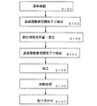
本実施の形態では、本発明の一態様であるスパッタリングターゲットの製造方法について図1を参照して説明する。図1は、本実施の形態に係るスパッタリングターゲットの製造方法の一例を示すフローチャートである。
(Embodiment 1)
In this embodiment, a method for manufacturing a sputtering target which is one embodiment of the present invention will be described with reference to FIGS. FIG. 1 is a flowchart showing an example of a method for manufacturing a sputtering target according to the present embodiment.
はじめに、スパッタリングターゲットの材料を構成する複数の単体金属(Zn、In、Al、Snなど)をそれぞれ蒸留、昇華、または再結晶を繰り返して精製する(S101)。その後、それぞれ精製した金属を粉末状に加工する。なお、スパッタリングターゲットの材料として、GaやSiを用いる場合は、ゾーンメルト法や、チョクラルスキー法を使って単結晶を得た後、粉末状に加工する。そして、これら各スパッタリングターゲット材料を高純度の酸素雰囲気下で焼成して酸化させる(S102)。そして得られた各酸化物粉末の秤量を適宜行い、秤量した各酸化物粉末を混合する(S103)。 First, a plurality of simple metals (Zn, In, Al, Sn, etc.) constituting the material of the sputtering target are purified by repeating distillation, sublimation, or recrystallization (S101). Thereafter, each refined metal is processed into powder. In addition, when using Ga and Si as a material of a sputtering target, after obtaining a single crystal using the zone melt method or the Czochralski method, it processes into a powder form. Each of these sputtering target materials is fired and oxidized in a high purity oxygen atmosphere (S102). The obtained oxide powders are weighed appropriately, and the weighed oxide powders are mixed (S103).
高純度の酸素雰囲気は、例えば6N(99.9999%)以上、好ましくは7N(99.99999%)以上、(即ち不純物濃度を1ppm以下、好ましくは0.1ppm以下)の純度とする。 The high-purity oxygen atmosphere has a purity of, for example, 6N (99.9999%) or more, preferably 7N (99.99999%) or more (that is, the impurity concentration is 1 ppm or less, preferably 0.1 ppm or less).
本実施の形態では、In−Ga−Zn系酸化物半導体用スパッタリングターゲットを製造するものとし、例えば、In2O3、Ga2O3、及びZnOを、組成比として、In2O3:Ga2O3:ZnO=1:1:1[mol数比]となるように秤量する。 In this embodiment, a sputtering target for an In—Ga—Zn-based oxide semiconductor is manufactured. For example, In 2 O 3 , Ga 2 O 3 , and ZnO are used as the composition ratio, and In 2 O 3 : Ga. Weigh so that 2 O 3 : ZnO = 1: 1: 1 [molar ratio].
また、本実施の形態において製造される酸化物半導体用スパッタリングターゲットとしては、In−Ga−Zn系酸化物半導体用スパッタリングターゲットに限られるものではなく、他にも、In−Sn−Ga−Zn系酸化物半導体用スパッタリングターゲット、In−Sn−Zn系酸化物半導体用スパッタリングターゲット、In−Al−Zn系酸化物半導体用スパッタリングターゲット、Sn−Ga−Zn系酸化物半導体用スパッタリングターゲット、Al−Ga−Zn系酸化物半導体用スパッタリングターゲット、Sn−Al−Zn系酸化物半導体用スパッタリングターゲット、In−Zn系酸化物半導体用スパッタリングターゲット、Sn−Zn系酸化物半導体用スパッタリングターゲット、Al−Zn系酸化物半導体用スパッタリングターゲット、In系酸化物半導体用スパッタリングターゲット、Sn系酸化物半導体用スパッタリングターゲット、Zn系酸化物半導体用スパッタリングターゲットなどが挙げられる。 The sputtering target for an oxide semiconductor manufactured in this embodiment is not limited to the sputtering target for an In—Ga—Zn-based oxide semiconductor, and other than that, the In—Sn—Ga—Zn-based sputtering target. Sputtering target for oxide semiconductor, sputtering target for In-Sn-Zn-based oxide semiconductor, sputtering target for In-Al-Zn-based oxide semiconductor, sputtering target for Sn-Ga-Zn-based oxide semiconductor, Al-Ga- Sputtering target for Zn-based oxide semiconductor, sputtering target for Sn-Al-Zn-based oxide semiconductor, sputtering target for In-Zn-based oxide semiconductor, sputtering target for Sn-Zn-based oxide semiconductor, Al-Zn-based oxide Spatter for semiconductors Grayed target, In-based oxide semiconductor sputtering target for, Sn-based oxide semiconductor, a sputtering target for such Zn-based oxide semiconductor sputtering target for the like.
次いで、混合物を所定の形状に成形し、焼成して、金属酸化物の焼結体を得る(S104)。スパッタリングターゲット材料を焼成することにより、スパッタリングターゲットに水素や水分やハイドロカーボン等が混入することを防ぐことが出来る。焼成は、不活性ガス雰囲気(窒素または希ガス雰囲気)下、真空中または高圧雰囲気中で行うことができ、さらに機械的な圧力を加えながら行ってもよい。焼成法としては、常圧焼成法、加圧焼成法等を適宜用いることができる。また、加圧焼成法としては、ホットプレス法、熱間等方加圧(HIP;Hot Isostatic Pressing)法、放電プラズマ焼結法、又は衝撃法を適用することが好ましい。焼成の最高温度はスパッタリングターゲット材料の焼結温度により選択するが、1000℃〜2000℃程度とするのが好ましく、1200℃〜1500℃とするのがより好ましい。また、最高温度の保持時間は、スパッタリングターゲット材料により選択するが、0.5時間〜3時間とするのが好ましい。 Next, the mixture is formed into a predetermined shape and fired to obtain a metal oxide sintered body (S104). By firing the sputtering target material, it is possible to prevent the sputtering target from being mixed with hydrogen, moisture, hydrocarbon, or the like. Firing can be performed in an inert gas atmosphere (nitrogen or rare gas atmosphere), in a vacuum or in a high-pressure atmosphere, and may be performed while applying mechanical pressure. As the firing method, a normal pressure firing method, a pressure firing method, or the like can be used as appropriate. As the pressure firing method, it is preferable to apply a hot pressing method, a hot isostatic pressing (HIP) method, a discharge plasma sintering method, or an impact method. Although the maximum temperature of baking is selected by the sintering temperature of sputtering target material, it is preferable to set it as about 1000 to 2000 degreeC, and it is more preferable to set it as 1200 to 1500 degreeC. The maximum temperature holding time is selected according to the sputtering target material, but is preferably 0.5 hours to 3 hours.
なお、本実施の形態の酸化物半導体用スパッタリングターゲットは充填率が90%以上100%以下、より好ましくは95%以上99.9%以下とするのが好ましい。 Note that the oxide semiconductor sputtering target of this embodiment has a filling rate of 90% to 100%, more preferably 95% to 99.9%.
次いで、所望の寸法、所望の形状、及び所望の表面粗さを有するスパッタリングターゲットに成形するための機械加工を施す(S105)。加工手段としては、例えば機械的研磨、化学的機械研磨(Chemical Mechanical Polishing CMP)、またはこれらの併用等を用いることができる。 Next, machining for forming a sputtering target having a desired dimension, a desired shape, and a desired surface roughness is performed (S105). As a processing means, for example, mechanical polishing, chemical mechanical polishing (CMP), or a combination thereof can be used.
次いで、機械加工によって発生する細かな塵や、研削液成分の除去のために洗浄をおこなってもよい。ただし、洗浄として水や有機溶媒に浸漬させた超音波洗浄、流水洗浄等によってスパッタリングターゲットを洗浄する場合、その後にターゲット中及び表面の含水素濃度が充分低減するための加熱処理を行うことが好ましい。 Next, cleaning may be performed to remove fine dust generated by machining and grinding fluid components. However, when the sputtering target is cleaned by ultrasonic cleaning immersed in water or an organic solvent as cleaning, running water cleaning, or the like, it is preferable to perform a heat treatment for sufficiently reducing the hydrogen-containing concentration in the target and on the surface thereafter. .
その後、スパッタリングターゲットに加熱処理を加える(S106)。加熱処理は、不活性ガス雰囲気(窒素または希ガス雰囲気)中で行うのが好ましく、加熱処理の温度は、スパッタリングターゲット材料によって異なるが、スパッタリングターゲット材料が変性しない温度とする。具体的には、150℃以上であって750℃以下、好ましくは425℃以上であって750℃以下とする。また、加熱時間は、具体的には0.5時間以上、好ましくは1時間以上とする。なお、加熱処理は、真空中または高圧雰囲気中で行ってもよい。 Thereafter, heat treatment is applied to the sputtering target (S106). The heat treatment is preferably performed in an inert gas atmosphere (nitrogen or rare gas atmosphere), and the temperature of the heat treatment varies depending on the sputtering target material, but is a temperature at which the sputtering target material is not denatured. Specifically, the temperature is 150 ° C. or higher and 750 ° C. or lower, preferably 425 ° C. or higher and 750 ° C. or lower. The heating time is specifically 0.5 hours or longer, preferably 1 hour or longer. Note that the heat treatment may be performed in a vacuum or in a high-pressure atmosphere.
その後、スパッタリングターゲットをバッキングプレートと呼ばれる金属板に貼り合わせる(S107)。バッキングプレートは、スパッタリングターゲット材料の冷却とスパッタ電極としての役割をもつため、熱伝導性および導電性に優れた銅を用いることが好ましい。また、銅以外にも、チタン、銅合金、ステンレス合金等を用いることも可能である。 Thereafter, the sputtering target is bonded to a metal plate called a backing plate (S107). Since the backing plate has a role of cooling the sputtering target material and serving as a sputtering electrode, it is preferable to use copper having excellent thermal conductivity and conductivity. In addition to copper, titanium, a copper alloy, a stainless alloy, or the like can also be used.
また、バッキングプレートにスパッタリングターゲットを貼り付ける際、スパッタリングターゲットを分割して一枚のバッキングプレートにボンディングしてもよい。図2(A)(B)にスパッタリングターゲットを分割して一枚のバッキングプレートに貼り付ける(ボンディング)する例を示す。 Further, when the sputtering target is attached to the backing plate, the sputtering target may be divided and bonded to a single backing plate. FIGS. 2A and 2B show an example in which a sputtering target is divided and attached (bonded) to a single backing plate.
図2(A)はバッキングプレート850にスパッタリングターゲット851をスパッタリングターゲット851a、851b、851c、851dと4分割して貼り付ける例である。また、図2(B)はより多数にスパッタリングターゲットを分割した例であり、バッキングプレート850にスパッタリングターゲット852をスパッタリングターゲット852a、852b、852c、852d、852e、852f、852g、852h、852iと9分割して貼り付けている。なお、スパッタリングターゲットの分割数及びターゲット形状は図2(A)(B)に限定されない。スパッタリングターゲットを分割するとバッキングプレートに貼り付ける際のスパッタリングターゲットの反りを緩和することができる。このような分割したスパッタリングターゲットは、大面積基板に成膜する場合、それに伴って大型化するスパッタリングターゲットに特に好適に用いることができる。もちろん、一枚のバッキングプレートに一枚のスパッタリングターゲットを貼り付けてもよい。
FIG. 2A illustrates an example in which a
また、加熱処理後のスパッタリングターゲットは、水分や水素やアルカリ金属などの不純物の再混入を防止するため、高純度の酸素ガス、高純度のN2Oガス、又は超乾燥エア(露点が−40℃以下、好ましくは−60℃以下)雰囲気で搬送、保存等するのが好ましい。または、ステンレス合金等の透水性の低い材料で形成された保護材で覆ってもよく、またその保護材とターゲットの間隙に上述のガスを導入しても良い。酸素ガスまたはN2Oガスには、水、水素などが含まれないことが好ましい。または、酸素ガスまたはN2Oガスの純度を、6N(99.9999%)以上、好ましくは7N(99.99999%)以上、(即ち酸素ガスまたはN2Oガス中の不純物濃度を1ppm以下、好ましくは0.1ppm以下)とすることが好ましい。 In addition, the sputtering target after heat treatment has a high-purity oxygen gas, a high-purity N 2 O gas, or ultra-dry air (with a dew point of −40) in order to prevent re-mixing of impurities such as moisture, hydrogen, and alkali metal. It is preferable to carry, store, etc. in an atmosphere (° C or lower, preferably -60 ° C or lower). Or you may cover with the protective material formed with materials with low water permeability, such as a stainless alloy, and you may introduce | transduce the above-mentioned gas into the clearance gap between the protective material and a target. The oxygen gas or N 2 O gas preferably does not contain water, hydrogen, or the like. Alternatively, the purity of the oxygen gas or N 2 O gas is 6N (99.9999%) or more, preferably 7N (99.99999%) or more (that is, the impurity concentration in the oxygen gas or N 2 O gas is 1 ppm or less, Preferably it is 0.1 ppm or less.
以上により、本実施の形態のスパッタリングターゲットを製造することができる。本実施の形態で示すスパッタリングターゲットは、製造工程において、それぞれ精製した高純度の材料を用いることで不純物の含有量の少ないものとすることができる。また、当該ターゲットを用いて作製された酸化物半導体膜が含有する不純物の濃度も低減することができる。 As described above, the sputtering target of this embodiment can be manufactured. The sputtering target shown in this embodiment can have a low impurity content by using purified high-purity materials in the manufacturing process. In addition, the concentration of impurities contained in the oxide semiconductor film manufactured using the target can be reduced.
また、上記スパッタリングターゲットの製造において、大気にさらさず不活性ガス雰囲気(窒素または希ガス雰囲気)下で行うことが好ましい。 In addition, the sputtering target is preferably manufactured under an inert gas atmosphere (nitrogen or a rare gas atmosphere) without being exposed to the air.
なお、スパッタリングターゲットをスパッタ装置に取り付ける際も、大気にさらさず不活性ガス雰囲気(窒素または希ガス雰囲気)下で行うことで、スパッタリングターゲットに水素や水分やアルカリ金属等が付着することを防ぐことができる。 In addition, when attaching the sputtering target to the sputtering apparatus, it is performed under an inert gas atmosphere (nitrogen or a rare gas atmosphere) without being exposed to the air to prevent hydrogen, moisture, alkali metal, etc. from adhering to the sputtering target. Can do.
また、スパッタリングターゲットをスパッタ装置に取り付けた後、ターゲット表面やターゲット材料中に残存している水素を除去するために脱水素処理を行うことが好ましい。脱水素処理としては成膜チャンバー内を減圧下で200℃〜600℃に加熱する方法や、加熱しながら窒素や不活性ガスの導入と排気を繰り返す方法等がある。 In addition, after the sputtering target is attached to the sputtering apparatus, it is preferable to perform a dehydrogenation process in order to remove hydrogen remaining on the target surface and the target material. As the dehydrogenation treatment, there are a method in which the inside of the film formation chamber is heated to 200 ° C. to 600 ° C. under reduced pressure, a method in which introduction and exhaust of nitrogen and an inert gas are repeated while heating, and the like.
また、スパッタリングターゲットを取り付けたスパッタ装置は、リークレートを1×10⁻¹⁰Pa・m3/秒以下とし、特に排気手段としてクライオポンプを用いて水の不純物としての混入を減らし、逆流防止も図ることが好ましい。 In addition, the sputtering apparatus to which the sputtering target is attached has a leak rate of 1 × 10 −10 Pa · m 3 / sec or less, and in particular, a cryopump is used as an evacuation unit to reduce contamination as water impurities and to prevent backflow. It is preferable.
以下に、上記フローにより得られたスパッタリングターゲットが取り付けられたスパッタ装置を用いてトランジスタを作製する例を図3を用いて説明する。トランジスタを作製する工程においても、スパッタ装置で成膜された酸化物半導体膜に対して、H2Oに代表される水素原子を含む化合物や、アルカリ金属を含む化合物、もしくはアルカリ土類金属を含む化合物等の不純物が混入しないようにすることが好ましい。 An example in which a transistor is manufactured using a sputtering apparatus to which a sputtering target obtained by the above flow is attached will be described below with reference to FIGS. In the process for manufacturing the transistor, the oxide semiconductor film formed with a sputtering apparatus includes a compound containing a hydrogen atom typified by H 2 O, a compound containing an alkali metal, or an alkaline earth metal. It is preferable to prevent impurities such as compounds from entering.
まず、絶縁表面を有する基板100上に導電膜を形成した後、第1のフォトリソグラフィ工程、及びエッチング工程によりゲート電極層112を形成する。
First, after a conductive film is formed over the
基板100とゲート電極層112との間には、下地膜となる絶縁膜を設けてもよく、本実施の形態では下地膜101を設ける。下地膜101は、基板100からの不純物元素(Naなど)の拡散を防止する機能があり、酸化シリコン、酸窒化シリコン、窒化シリコン、酸化ハフニウム、酸化アルミニウム、酸化ガリウム、酸化ガリウムアルミニウム(GaxAl2−xO3+y(xは0以上2以下、yは0より大きく、1未満))から選ばれた膜で形成することができる。下地膜101を設けることによって、後に形成する酸化物半導体膜に基板100からの不純物元素(Naなど)が拡散されることをブロックできる。また、該下地膜は単層に限らず、上記の複数の膜の積層であっても良い。
An insulating film serving as a base film may be provided between the
次いで、ゲート電極層112上に、スパッタリング法またはPCVD法によりゲート絶縁層102を形成する(図3(A)参照)。ゲート絶縁層102の形成時も、アルカリ金属を含む化合物、もしくはアルカリ土類金属を含む化合物等の不純物が混入しないようにすることが好ましく、下地膜101の成膜後、大気にふれることなくゲート絶縁層102を形成する。
Next, the
次いで、上記ゲート絶縁層102を形成した後、大気に触れることなく、ゲート絶縁層102上に膜厚1nm以上10nm以下の第1の酸化物半導体膜をスパッタリング法により形成する。本実施の形態では、酸化物半導体用ターゲット(In−Ga−Zn系酸化物半導体用ターゲット(In2O3:Ga2O3:ZnO=1:1:2[mol数比])を用いて、基板とターゲットの間との距離を170mm、基板温度250℃、圧力0.4Pa、直流(DC)電源0.5kW、酸素のみ、アルゴンのみ、又はアルゴン及び酸素雰囲気下で膜厚5nmの第1の酸化物半導体膜を成膜する。酸化物半導体用ターゲットは、酸化亜鉛、酸化アルミニウム、酸化ガリウム、酸化インジウム、または酸化スズから選ばれた少なくとも一の酸化物の焼結体を含み、SIMSにおける前記焼結体の含有アルカリ金属濃度が5×1016cm−3以下とする。また、前記焼結体は、SIMSにおけるNaの濃度が5×1016cm−3以下、好ましくは1×1016cm−3以下、さらに好ましくは1×1015cm−3以下とする。また、前記焼結体は、SIMSにおけるLiの濃度が5×1015cm−3以下、好ましくは1×1015cm−3以下とする。また、前記焼結体は、SIMSにおけるKの濃度が5×1015cm−3以下、好ましくは1×1015cm−3以下とする。
Next, after the
次いで、上記第1の酸化物半導体膜を成膜後、大気に触れることなく、基板を配置する雰囲気を窒素、または乾燥空気とし、第1の加熱処理を行う。第1の加熱処理の温度は、400℃以上750℃以下とする。また、第1の加熱処理の加熱時間は1分以上24時間以下とする。第1の加熱処理によって第1の結晶性酸化物半導体膜108aを形成する(図3(B)参照)。
Next, after the first oxide semiconductor film is formed, the first heat treatment is performed with the atmosphere in which the substrate is placed being nitrogen or dry air without being exposed to the air. The temperature of the first heat treatment is 400 ° C. or higher and 750 ° C. or lower. The heating time for the first heat treatment is 1 minute to 24 hours. The first crystalline
次いで、上記第1の加熱処理後に大気に触れることなく、第1の結晶性酸化物半導体膜108a上に10nmよりも厚い第2の酸化物半導体膜をスパッタリング法により形成する。本実施の形態では、酸化物半導体用ターゲット(In−Ga−Zn系酸化物半導体用ターゲット(In2O3:Ga2O3:ZnO=1:1:2[mol数比])を用いて、基板とターゲットの間との距離を170mm、基板温度400℃、圧力0.4Pa、直流(DC)電源0.5kW、酸素のみ、アルゴンのみ、又はアルゴン及び酸素雰囲気下で膜厚25nmの第2の酸化物半導体膜を成膜する。酸化物半導体用ターゲットは、酸化亜鉛、酸化アルミニウム、酸化ガリウム、酸化インジウム、または酸化スズから選ばれた少なくとも一の酸化物の焼結体を含み、SIMSにおける前記焼結体の含有アルカリ金属濃度が5×1016cm−3以下とする。また、前記焼結体は、SIMSにおけるNaの濃度が5×1016cm−3以下、好ましくは1×1016cm−3以下、さらに好ましくは1×1015cm−3以下とする。また、前記焼結体は、SIMSにおけるLiの濃度が5×1015cm−3以下、好ましくは1×1015cm−3以下とする。また、前記焼結体は、SIMSにおけるKの濃度が5×1015cm−3以下、好ましくは1×1015cm−3以下とする。
Next, a second oxide semiconductor film having a thickness greater than 10 nm is formed over the first crystalline
なお、第1の酸化物半導体膜及び第2の酸化物半導体膜の成膜時において、H2Oに代表される水素原子を含む化合物や、アルカリ金属を含む化合物、もしくはアルカリ土類金属を含む化合物等の不純物が混入しないようにすることが好ましく、具体的には、基板とターゲットの間との距離(TS距離とも呼ぶ)を長くすることによって質量の重い不純物元素を排気し、成膜中での混入を低減する、または成膜室内を高真空として基板上に付着したH2Oなどを膜形成面から再蒸発させる。また、成膜時の基板温度を250℃以上450℃以下とすることによって、H2Oに代表される水素原子を含む化合物や、アルカリ金属を含む化合物、もしくはアルカリ土類金属を含む化合物等の不純物が酸化物半導体膜中に混入することを防ぐことが好ましい。 Note that in the formation of the first oxide semiconductor film and the second oxide semiconductor film, a compound containing a hydrogen atom typified by H 2 O, a compound containing an alkali metal, or an alkaline earth metal is included. It is preferable to prevent impurities such as compounds from being mixed. Specifically, by increasing the distance between the substrate and the target (also referred to as the TS distance), the heavy impurity element is exhausted and the film is being formed. Or by re-evaporating H 2 O or the like adhering to the substrate from the film formation surface. In addition, by setting the substrate temperature during film formation to 250 ° C. or more and 450 ° C. or less, a compound containing a hydrogen atom typified by H 2 O, a compound containing an alkali metal, or a compound containing an alkaline earth metal, etc. It is preferable to prevent impurities from entering the oxide semiconductor film.
次いで、上記第2の酸化物半導体膜を成膜後、大気に触れることなく、基板を配置する雰囲気を窒素、または乾燥空気とし、第2の加熱処理を行う。第2の加熱処理の温度は、400℃以上750℃以下とする。また、第2の加熱処理の加熱時間は1分以上24時間以下とする。第2の加熱処理によって第2の結晶性酸化物半導体膜108bを形成する(図3(C)参照)。
Next, after the second oxide semiconductor film is formed, the atmosphere in which the substrate is placed is set to nitrogen or dry air without being exposed to the air, and second heat treatment is performed. The temperature of the second heat treatment is 400 ° C to 750 ° C. The heating time for the second heat treatment is 1 minute to 24 hours. The second crystalline
次いで、第1の結晶性酸化物半導体膜108aと第2の結晶性酸化物半導体膜108bからなる酸化物半導体積層を加工して島状の酸化物半導体積層を形成する(図3(D)参照)。
Next, the oxide semiconductor stack including the first crystalline
酸化物半導体積層の加工は、所望の形状のマスクを酸化物半導体積層上に形成した後、当該酸化物半導体積層をエッチングすることによって行うことができる。上述のマスクは、フォトリソグラフィなどの方法を用いて形成することができる。または、インクジェット法などの方法を用いてマスクを形成しても良い。 The oxide semiconductor stack can be processed by forming a mask having a desired shape over the oxide semiconductor stack and then etching the oxide semiconductor stack. The above-described mask can be formed using a method such as photolithography. Alternatively, the mask may be formed using a method such as an inkjet method.
なお、酸化物半導体積層のエッチングは、ドライエッチングでもウェットエッチングでもよい。もちろん、これらを組み合わせて用いてもよい。 Note that etching of the oxide semiconductor stack may be dry etching or wet etching. Of course, these may be used in combination.
次いで、酸化物半導体積層上にソース電極層およびドレイン電極層(これと同じ層で形成される配線を含む)を形成するための導電膜を形成し、当該導電膜を加工して、ソース電極層104aおよびドレイン電極層104bを形成する。
Next, a conductive film for forming a source electrode layer and a drain electrode layer (including a wiring formed using the same layer) is formed over the oxide semiconductor stack, the conductive film is processed, and the
次いで、酸化物半導体積層、ソース電極層104a、及びドレイン電極層104bを覆う絶縁膜110a、絶縁膜110bを形成する(図3(E)参照)。絶縁膜110aは、酸化物絶縁材料を用い、成膜後に第3の加熱処理を行うことが好ましい。第3の加熱処理によって、絶縁膜110aから酸化物半導体積層への酸素供給が行われる。第3の加熱処理の条件は、不活性雰囲気、酸素雰囲気、酸素と窒素の混合雰囲気下で、200℃以上400℃、好ましくは250℃以上320℃以下とする。また、第3の加熱処理の加熱時間は1分以上24時間以下とする。
Next, the insulating
以上の工程でボトムゲート型のトランジスタ150が形成される。
Through the above process, the
トランジスタ150は、絶縁表面を有する基板100上に、下地膜101、ゲート電極層112、ゲート絶縁層102、チャネル形成領域を含む酸化物半導体積層、ソース電極層104a、ドレイン電極層104b、絶縁膜110aを含む。酸化物半導体積層を覆ってソース電極層104a、及びドレイン電極層104bが設けられる。酸化物半導体積層において、ゲート絶縁層102を介してゲート電極層112と重なる領域の一部がチャネル形成領域として機能する。
The
図3(E)に示すトランジスタ150のチャネル形成領域を含む半導体層(上記、酸化物半導体積層を指す)は、SIMSにおけるNaの濃度が5×1016cm−3以下、好ましくは1×1016cm−3以下、さらに好ましくは1×1015cm−3以下とする。また、トランジスタ150のチャネル形成領域を含む半導体層は、SIMSにおけるLiの濃度が5×1015cm−3以下、好ましくは1×1015cm−3以下とする。また、トランジスタ150のチャネル形成領域を含む半導体層は、SIMSにおけるKの濃度が5×1015cm−3以下、好ましくは1×1015cm−3以下とする。
In the semiconductor layer including the channel formation region of the
また、図3(E)に示すトランジスタ150のチャネル形成領域を含む半導体層は、SIMSにおける水素の濃度が5×1019cm−3以下、特に5×1018cm−3以下とすることが好ましい。
In addition, the semiconductor layer including the channel formation region of the
また、図3(E)に示すトランジスタ150のチャネル形成領域を含む半導体層は、第1の結晶性酸化物半導体膜108a、及び第2の結晶性酸化物半導体膜108bの積層となる。第1の結晶性酸化物半導体膜108a、及び第2の結晶性酸化物半導体膜108bは、c軸配向を有している。第1の結晶性酸化物半導体膜108a及び第2の結晶性酸化物半導体膜108bは、単結晶構造ではなく、非晶質構造でもない構造であり、c軸配向を有した結晶(C Axis Aligned Crystal; CAACとも呼ぶ)を含む酸化物を有する。なお、第1の結晶性酸化物半導体膜108a及び第2の結晶性酸化物半導体膜108bは、一部に結晶粒界を有しており、非晶質構造(アモフルファス構造)の酸化物半導体膜とは明らかに別材料である。
In addition, the semiconductor layer including the channel formation region of the
第1の結晶性酸化物半導体膜と第2の結晶性酸化物半導体膜の積層を有するトランジスタは、トランジスタに光照射が行われ、またはバイアス−熱ストレス(BT)試験前後においてもトランジスタのしきい値電圧の変化量が低減でき、安定した電気的特性を有する。 In the transistor including a stack of the first crystalline oxide semiconductor film and the second crystalline oxide semiconductor film, the transistor is irradiated with light or the threshold of the transistor before and after the bias-thermal stress (BT) test. The amount of change in value voltage can be reduced, and stable electrical characteristics are obtained.
なお、図3では、ボトムゲート型のトランジスタの例を示したが特に限定されず、例えばトップゲート型のトランジスタを作製することもできる。 Note that FIG. 3 illustrates an example of a bottom-gate transistor, but the invention is not particularly limited. For example, a top-gate transistor can be manufactured.
100 基板
101 下地膜
102 ゲート絶縁層
104a ソース電極層
104b ドレイン電極層
108a 第1の結晶性酸化物半導体膜
108b 第2の結晶性酸化物半導体膜
110a 絶縁膜
110b 絶縁膜
112 ゲート電極層
150 トランジスタ
850 バッキングプレート
851 スパッタリングターゲット
851a スパッタリングターゲット
851b スパッタリングターゲット
851c スパッタリングターゲット
851d スパッタリングターゲット
852 スパッタリングターゲット
852a スパッタリングターゲット
852b スパッタリングターゲット
852c スパッタリングターゲット
852d スパッタリングターゲット
852e スパッタリングターゲット
852f スパッタリングターゲット
852g スパッタリングターゲット
852h スパッタリングターゲット
852i スパッタリングターゲット
100
Claims (8)
ゲート絶縁膜を形成する工程と、
スパッタリングターゲットを用いてスパッタリング法によって酸化物半導体膜を形成する工程と、
前記酸化物半導体膜に対して加熱処理を行う工程と、を有し、
前記スパッタリングターゲットは、酸化亜鉛、酸化アルミニウム、酸化ガリウム、酸化インジウム、または酸化スズから選ばれた少なくとも一の酸化物の焼結体を含み、
SIMSにおける前記焼結体の含有アルカリ金属濃度は、5×1016cm−3以下であり、
前記加熱処理後の前記酸化物半導体膜は、c軸配向を有する結晶を含むことを特徴とする半導体装置の作製方法。 Forming a gate electrode;
Forming a gate insulating film;
Forming an oxide semiconductor film by a sputtering method using a spatter ring target,
And a step of performing a heat treatment on the oxide semiconductor film,
The sputtering target includes a sintered body of at least one oxide selected from zinc oxide, aluminum oxide, gallium oxide, indium oxide, or tin oxide,
Containing alkali metal concentration of the sintered body in the SIMS state, and are 5 × 10 16 cm -3,
The method for manufacturing a semiconductor device, wherein the oxide semiconductor film after the heat treatment includes a crystal having c-axis orientation .
ゲート絶縁膜を形成する工程と、
スパッタリングターゲットを用いてスパッタリング法によって酸化物半導体膜を形成する工程と、
前記酸化物半導体膜に対して加熱処理を行う工程と、を有し、
前記スパッタリングターゲットは、酸化亜鉛、酸化アルミニウム、酸化ガリウム、酸化インジウム、または酸化スズから選ばれた少なくとも一の酸化物の焼結体を含み、
SIMSにおける前記焼結体の含有アルカリ金属濃度は、5×1016cm−3以下であり、且つ、SIMSにおける前記焼結体の含有水素濃度は、1×1019cm−3以下であり、
前記加熱処理後の前記酸化物半導体膜は、c軸配向を有する結晶を含むことを特徴とする半導体装置の作製方法。 Forming a gate electrode;
Forming a gate insulating film;
Forming an oxide semiconductor film by a sputtering method using a spatter ring target,
And a step of performing a heat treatment on the oxide semiconductor film,
The sputtering target includes a sintered body of at least one oxide selected from zinc oxide, aluminum oxide, gallium oxide, indium oxide, or tin oxide,
Containing alkali metal concentration of the sintered body in SIMS is a 5 × 10 16 cm -3 or less, and, hydrogen concentration of the sintered body in the SIMS state, and are 1 × 10 19 cm -3 or less,
The method for manufacturing a semiconductor device, wherein the oxide semiconductor film after the heat treatment includes a crystal having c-axis orientation .
SIMSにおける前記焼結体の含有ナトリウム濃度は、1×1016cm−3以下であることを特徴とする半導体装置の作製方法。 In claim 1 or claim 2,
The method for manufacturing a semiconductor device, wherein a concentration of sodium contained in the sintered body in SIMS is 1 × 10 16 cm −3 or less.
SIMSにおける前記焼結体の含有ナトリウム濃度は、1×1015cm−3以下であることを特徴とする半導体装置の作製方法。 In claim 1 or claim 2,
A method for manufacturing a semiconductor device, wherein a concentration of sodium contained in the sintered body in SIMS is 1 × 10 15 cm −3 or less.
SIMSにおける前記焼結体の含有リチウム濃度は、5×1015cm−3以下であることを特徴とする半導体装置の作製方法。 In any one of Claims 1 thru | or 4,
The method for manufacturing a semiconductor device, wherein a concentration of lithium contained in the sintered body in SIMS is 5 × 10 15 cm −3 or less.
SIMSにおける前記焼結体の含有リチウム濃度は、1×1015cm−3以下であることを特徴とする半導体装置の作製方法。 In any one of Claims 1 thru | or 4,
The method for manufacturing a semiconductor device, wherein the concentration of lithium contained in the sintered body in SIMS is 1 × 10 15 cm −3 or less.
SIMSにおける前記焼結体の含有カリウム濃度は、5×1015cm−3以下であることを特徴とする半導体装置の作製方法。 In any one of Claims 1 thru | or 6,
The method for manufacturing a semiconductor device, wherein a concentration of potassium contained in the sintered body in SIMS is 5 × 10 15 cm −3 or less.
SIMSにおける前記焼結体の含有カリウム濃度は、1×1015cm−3以下であることを特徴とする半導体装置の作製方法。 In any one of Claims 1 thru | or 6,
The method for manufacturing a semiconductor device, wherein a concentration of potassium contained in the sintered body in SIMS is 1 × 10 15 cm −3 or less.
Priority Applications (1)
| Application Number | Priority Date | Filing Date | Title |
|---|---|---|---|
| JP2011187729A JP5789157B2 (en) | 2010-09-03 | 2011-08-30 | Method for manufacturing semiconductor device |
Applications Claiming Priority (3)
| Application Number | Priority Date | Filing Date | Title |
|---|---|---|---|
| JP2010197509 | 2010-09-03 | ||
| JP2010197509 | 2010-09-03 | ||
| JP2011187729A JP5789157B2 (en) | 2010-09-03 | 2011-08-30 | Method for manufacturing semiconductor device |
Related Child Applications (1)
| Application Number | Title | Priority Date | Filing Date |
|---|---|---|---|
| JP2015151789A Division JP2015187312A (en) | 2010-09-03 | 2015-07-31 | sputtering target |
Publications (3)
| Publication Number | Publication Date |
|---|---|
| JP2012072493A JP2012072493A (en) | 2012-04-12 |
| JP2012072493A5 JP2012072493A5 (en) | 2014-08-28 |
| JP5789157B2 true JP5789157B2 (en) | 2015-10-07 |
Family
ID=45770024
Family Applications (3)
| Application Number | Title | Priority Date | Filing Date |
|---|---|---|---|
| JP2011187729A Active JP5789157B2 (en) | 2010-09-03 | 2011-08-30 | Method for manufacturing semiconductor device |
| JP2015151789A Withdrawn JP2015187312A (en) | 2010-09-03 | 2015-07-31 | sputtering target |
| JP2016246486A Expired - Fee Related JP6397878B2 (en) | 2010-09-03 | 2016-12-20 | Method for manufacturing semiconductor device |
Family Applications After (2)
| Application Number | Title | Priority Date | Filing Date |
|---|---|---|---|
| JP2015151789A Withdrawn JP2015187312A (en) | 2010-09-03 | 2015-07-31 | sputtering target |
| JP2016246486A Expired - Fee Related JP6397878B2 (en) | 2010-09-03 | 2016-12-20 | Method for manufacturing semiconductor device |
Country Status (5)
| Country | Link |
|---|---|
| US (3) | US8835214B2 (en) |
| JP (3) | JP5789157B2 (en) |
| KR (1) | KR20130099074A (en) |
| TW (1) | TWI570808B (en) |
| WO (1) | WO2012029612A1 (en) |
Families Citing this family (16)
| Publication number | Priority date | Publication date | Assignee | Title |
|---|---|---|---|---|
| US8894825B2 (en) | 2010-12-17 | 2014-11-25 | Semiconductor Energy Laboratory Co., Ltd. | Sputtering target, method for manufacturing the same, manufacturing semiconductor device |
| US9057126B2 (en) | 2011-11-29 | 2015-06-16 | Semiconductor Energy Laboratory Co., Ltd. | Method for manufacturing sputtering target and method for manufacturing semiconductor device |
| JP5795551B2 (en) * | 2012-05-14 | 2015-10-14 | 富士フイルム株式会社 | Method for manufacturing field effect transistor |
| KR102113160B1 (en) * | 2012-06-15 | 2020-05-20 | 가부시키가이샤 한도오따이 에네루기 켄큐쇼 | Semiconductor device |
| SG11201505097QA (en) * | 2012-06-29 | 2015-08-28 | Semiconductor Energy Lab | Method for using sputtering target and method for manufacturing oxide film |
| KR101389911B1 (en) | 2012-06-29 | 2014-04-29 | 삼성디스플레이 주식회사 | Thin film transistor and zinc oxide based sputtering target for the same |
| JP5965338B2 (en) | 2012-07-17 | 2016-08-03 | 出光興産株式会社 | Sputtering target, oxide semiconductor thin film, and manufacturing method thereof |
| JP6134230B2 (en) * | 2012-08-31 | 2017-05-24 | 株式会社神戸製鋼所 | Thin film transistor and display device |
| US8927985B2 (en) | 2012-09-20 | 2015-01-06 | Semiconductor Energy Laboratory Co., Ltd. | Semiconductor device |
| JP6284710B2 (en) * | 2012-10-18 | 2018-02-28 | 出光興産株式会社 | Sputtering target, oxide semiconductor thin film, and manufacturing method thereof |
| US9263531B2 (en) * | 2012-11-28 | 2016-02-16 | Semiconductor Energy Laboratory Co., Ltd. | Oxide semiconductor film, film formation method thereof, and semiconductor device |
| JP6141777B2 (en) | 2013-02-28 | 2017-06-07 | 株式会社半導体エネルギー研究所 | Method for manufacturing semiconductor device |
| JP6180908B2 (en) * | 2013-12-06 | 2017-08-16 | 富士フイルム株式会社 | Metal oxide semiconductor film, thin film transistor, display device, image sensor and X-ray sensor |
| CN107919365B (en) * | 2017-11-21 | 2019-10-11 | 深圳市华星光电半导体显示技术有限公司 | Carry on the back channel etch type TFT substrate and preparation method thereof |
| TWI756535B (en) * | 2019-04-15 | 2022-03-01 | 久盛光電股份有限公司 | Magnetron sputtering system and magnetron sputtering method |
| JP7317282B2 (en) * | 2019-07-19 | 2023-07-31 | 日新電機株式会社 | Method for manufacturing thin film transistor |
Family Cites Families (127)
| Publication number | Priority date | Publication date | Assignee | Title |
|---|---|---|---|---|
| JPS60198861A (en) | 1984-03-23 | 1985-10-08 | Fujitsu Ltd | Thin film transistor |
| JPH0244256B2 (en) | 1987-01-28 | 1990-10-03 | Kagaku Gijutsucho Mukizaishitsu Kenkyushocho | INGAZN2O5DESHIMESARERUROTSUHOSHOKEINOSOJOKOZOOJUSURUKAGOBUTSUOYOBISONOSEIZOHO |
| JPH0244258B2 (en) | 1987-02-24 | 1990-10-03 | Kagaku Gijutsucho Mukizaishitsu Kenkyushocho | INGAZN3O6DESHIMESARERUROTSUHOSHOKEINOSOJOKOZOOJUSURUKAGOBUTSUOYOBISONOSEIZOHO |
| JPS63210023A (en) | 1987-02-24 | 1988-08-31 | Natl Inst For Res In Inorg Mater | Compound having laminar structure of hexagonal crystal system expressed by ingazn4o7 and its production |
| JPH0244260B2 (en) | 1987-02-24 | 1990-10-03 | Kagaku Gijutsucho Mukizaishitsu Kenkyushocho | INGAZN5O8DESHIMESARERUROTSUHOSHOKEINOSOJOKOZOOJUSURUKAGOBUTSUOYOBISONOSEIZOHO |
| JPH0244262B2 (en) | 1987-02-27 | 1990-10-03 | Kagaku Gijutsucho Mukizaishitsu Kenkyushocho | INGAZN6O9DESHIMESARERUROTSUHOSHOKEINOSOJOKOZOOJUSURUKAGOBUTSUOYOBISONOSEIZOHO |
| JPH0244263B2 (en) | 1987-04-22 | 1990-10-03 | Kagaku Gijutsucho Mukizaishitsu Kenkyushocho | INGAZN7O10DESHIMESARERUROTSUHOSHOKEINOSOJOKOZOOJUSURUKAGOBUTSUOYOBISONOSEIZOHO |
| JPH05251705A (en) | 1992-03-04 | 1993-09-28 | Fuji Xerox Co Ltd | Thin-film transistor |
| JP3479375B2 (en) | 1995-03-27 | 2003-12-15 | 科学技術振興事業団 | Metal oxide semiconductor device in which a pn junction is formed with a thin film transistor made of a metal oxide semiconductor such as cuprous oxide, and methods for manufacturing the same |
| DE69635107D1 (en) | 1995-08-03 | 2005-09-29 | Koninkl Philips Electronics Nv | SEMICONDUCTOR ARRANGEMENT WITH A TRANSPARENT CIRCUIT ELEMENT |
| JP3625598B2 (en) | 1995-12-30 | 2005-03-02 | 三星電子株式会社 | Manufacturing method of liquid crystal display device |
| JP4170454B2 (en) | 1998-07-24 | 2008-10-22 | Hoya株式会社 | Article having transparent conductive oxide thin film and method for producing the same |
| JP2000150861A (en) | 1998-11-16 | 2000-05-30 | Tdk Corp | Oxide thin film |
| JP3276930B2 (en) | 1998-11-17 | 2002-04-22 | 科学技術振興事業団 | Transistor and semiconductor device |
| JP4230594B2 (en) * | 1999-03-05 | 2009-02-25 | 出光興産株式会社 | Sputtering target, transparent conductive glass and transparent conductive film |
| TW460731B (en) | 1999-09-03 | 2001-10-21 | Ind Tech Res Inst | Electrode structure and production method of wide viewing angle LCD |
| JP4089858B2 (en) | 2000-09-01 | 2008-05-28 | 国立大学法人東北大学 | Semiconductor device |
| KR20020038482A (en) | 2000-11-15 | 2002-05-23 | 모리시타 요이찌 | Thin film transistor array, method for producing the same, and display panel using the same |
| JP3997731B2 (en) | 2001-03-19 | 2007-10-24 | 富士ゼロックス株式会社 | Method for forming a crystalline semiconductor thin film on a substrate |
| JP2002289859A (en) | 2001-03-23 | 2002-10-04 | Minolta Co Ltd | Thin-film transistor |
| JP4090716B2 (en) | 2001-09-10 | 2008-05-28 | 雅司 川崎 | Thin film transistor and matrix display device |
| JP3925839B2 (en) | 2001-09-10 | 2007-06-06 | シャープ株式会社 | Semiconductor memory device and test method thereof |
| US7061014B2 (en) | 2001-11-05 | 2006-06-13 | Japan Science And Technology Agency | Natural-superlattice homologous single crystal thin film, method for preparation thereof, and device using said single crystal thin film |
| JP4164562B2 (en) | 2002-09-11 | 2008-10-15 | 独立行政法人科学技術振興機構 | Transparent thin film field effect transistor using homologous thin film as active layer |
| JP4083486B2 (en) | 2002-02-21 | 2008-04-30 | 独立行政法人科学技術振興機構 | Method for producing LnCuO (S, Se, Te) single crystal thin film |
| CN1445821A (en) | 2002-03-15 | 2003-10-01 | 三洋电机株式会社 | Forming method of ZnO film and ZnO semiconductor layer, semiconductor element and manufacturing method thereof |
| JP3933591B2 (en) | 2002-03-26 | 2007-06-20 | 淳二 城戸 | Organic electroluminescent device |
| US7339187B2 (en) | 2002-05-21 | 2008-03-04 | State Of Oregon Acting By And Through The Oregon State Board Of Higher Education On Behalf Of Oregon State University | Transistor structures |
| JP2004022625A (en) | 2002-06-13 | 2004-01-22 | Murata Mfg Co Ltd | Manufacturing method of semiconductor device and its manufacturing method |
| US7105868B2 (en) | 2002-06-24 | 2006-09-12 | Cermet, Inc. | High-electron mobility transistor with zinc oxide |
| US7067843B2 (en) | 2002-10-11 | 2006-06-27 | E. I. Du Pont De Nemours And Company | Transparent oxide semiconductor thin film transistors |
| JP4166105B2 (en) | 2003-03-06 | 2008-10-15 | シャープ株式会社 | Semiconductor device and manufacturing method thereof |
| JP2004273732A (en) | 2003-03-07 | 2004-09-30 | Sharp Corp | Active matrix substrate and its producing process |
| JP4108633B2 (en) | 2003-06-20 | 2008-06-25 | シャープ株式会社 | THIN FILM TRANSISTOR, MANUFACTURING METHOD THEREOF, AND ELECTRONIC DEVICE |
| US7262463B2 (en) | 2003-07-25 | 2007-08-28 | Hewlett-Packard Development Company, L.P. | Transistor including a deposited channel region having a doped portion |
| KR100753329B1 (en) | 2003-09-30 | 2007-08-29 | 닛코킨조쿠 가부시키가이샤 | High purity zinc oxide powder and method for production thereof, and high purity zinc oxide target and thin film of high purity zinc oxide |
| US7145174B2 (en) | 2004-03-12 | 2006-12-05 | Hewlett-Packard Development Company, Lp. | Semiconductor device |
| CN102856390B (en) | 2004-03-12 | 2015-11-25 | 独立行政法人科学技术振兴机构 | Comprise the LCD of thin-film transistor or the transition components of OLED display |
| US7297977B2 (en) | 2004-03-12 | 2007-11-20 | Hewlett-Packard Development Company, L.P. | Semiconductor device |
| US7282782B2 (en) | 2004-03-12 | 2007-10-16 | Hewlett-Packard Development Company, L.P. | Combined binary oxide semiconductor device |
| US7211825B2 (en) | 2004-06-14 | 2007-05-01 | Yi-Chi Shih | Indium oxide-based thin film transistors and circuits |
| JP2006100760A (en) | 2004-09-02 | 2006-04-13 | Casio Comput Co Ltd | Thin-film transistor and its manufacturing method |
| US7285501B2 (en) | 2004-09-17 | 2007-10-23 | Hewlett-Packard Development Company, L.P. | Method of forming a solution processed device |
| US7298084B2 (en) | 2004-11-02 | 2007-11-20 | 3M Innovative Properties Company | Methods and displays utilizing integrated zinc oxide row and column drivers in conjunction with organic light emitting diodes |
| US7829444B2 (en) | 2004-11-10 | 2010-11-09 | Canon Kabushiki Kaisha | Field effect transistor manufacturing method |
| EP1812969B1 (en) | 2004-11-10 | 2015-05-06 | Canon Kabushiki Kaisha | Field effect transistor comprising an amorphous oxide |
| US7791072B2 (en) | 2004-11-10 | 2010-09-07 | Canon Kabushiki Kaisha | Display |
| US7453065B2 (en) | 2004-11-10 | 2008-11-18 | Canon Kabushiki Kaisha | Sensor and image pickup device |
| WO2006051994A2 (en) | 2004-11-10 | 2006-05-18 | Canon Kabushiki Kaisha | Light-emitting device |
| BRPI0517560B8 (en) | 2004-11-10 | 2018-12-11 | Canon Kk | field effect transistor |
| US7863611B2 (en) | 2004-11-10 | 2011-01-04 | Canon Kabushiki Kaisha | Integrated circuits utilizing amorphous oxides |
| US7579224B2 (en) | 2005-01-21 | 2009-08-25 | Semiconductor Energy Laboratory Co., Ltd. | Method for manufacturing a thin film semiconductor device |
| TWI569441B (en) | 2005-01-28 | 2017-02-01 | 半導體能源研究所股份有限公司 | Semiconductor device, electronic device, and method of manufacturing semiconductor device |
| TWI472037B (en) | 2005-01-28 | 2015-02-01 | Semiconductor Energy Lab | Semiconductor device, electronic device, and method of manufacturing semiconductor device |
| US7858451B2 (en) | 2005-02-03 | 2010-12-28 | Semiconductor Energy Laboratory Co., Ltd. | Electronic device, semiconductor device and manufacturing method thereof |
| US7948171B2 (en) | 2005-02-18 | 2011-05-24 | Semiconductor Energy Laboratory Co., Ltd. | Light emitting device |
| US20060197092A1 (en) | 2005-03-03 | 2006-09-07 | Randy Hoffman | System and method for forming conductive material on a substrate |
| US8681077B2 (en) | 2005-03-18 | 2014-03-25 | Semiconductor Energy Laboratory Co., Ltd. | Semiconductor device, and display device, driving method and electronic apparatus thereof |
| US7544967B2 (en) | 2005-03-28 | 2009-06-09 | Massachusetts Institute Of Technology | Low voltage flexible organic/transparent transistor for selective gas sensing, photodetecting and CMOS device applications |
| US7645478B2 (en) | 2005-03-31 | 2010-01-12 | 3M Innovative Properties Company | Methods of making displays |
| US8300031B2 (en) | 2005-04-20 | 2012-10-30 | Semiconductor Energy Laboratory Co., Ltd. | Semiconductor device comprising transistor having gate and drain connected through a current-voltage conversion element |
| JP2006344849A (en) | 2005-06-10 | 2006-12-21 | Casio Comput Co Ltd | Thin film transistor |
| US7402506B2 (en) | 2005-06-16 | 2008-07-22 | Eastman Kodak Company | Methods of making thin film transistors comprising zinc-oxide-based semiconductor materials and transistors made thereby |
| US7691666B2 (en) | 2005-06-16 | 2010-04-06 | Eastman Kodak Company | Methods of making thin film transistors comprising zinc-oxide-based semiconductor materials and transistors made thereby |
| US7507618B2 (en) | 2005-06-27 | 2009-03-24 | 3M Innovative Properties Company | Method for making electronic devices using metal oxide nanoparticles |
| KR100711890B1 (en) | 2005-07-28 | 2007-04-25 | 삼성에스디아이 주식회사 | Organic Light Emitting Display and Fabrication Method for the same |
| JP2007059128A (en) | 2005-08-23 | 2007-03-08 | Canon Inc | Organic electroluminescent display device and manufacturing method thereof |
| JP2007073705A (en) | 2005-09-06 | 2007-03-22 | Canon Inc | Oxide-semiconductor channel film transistor and its method of manufacturing same |
| JP4280736B2 (en) | 2005-09-06 | 2009-06-17 | キヤノン株式会社 | Semiconductor element |
| JP5116225B2 (en) | 2005-09-06 | 2013-01-09 | キヤノン株式会社 | Manufacturing method of oxide semiconductor device |
| JP4850457B2 (en) | 2005-09-06 | 2012-01-11 | キヤノン株式会社 | Thin film transistor and thin film diode |
| JP5078246B2 (en) | 2005-09-29 | 2012-11-21 | 株式会社半導体エネルギー研究所 | Semiconductor device and manufacturing method of semiconductor device |
| JP5064747B2 (en) | 2005-09-29 | 2012-10-31 | 株式会社半導体エネルギー研究所 | Semiconductor device, electrophoretic display device, display module, electronic device, and method for manufacturing semiconductor device |
| EP1770788A3 (en) | 2005-09-29 | 2011-09-21 | Semiconductor Energy Laboratory Co., Ltd. | Semiconductor device having oxide semiconductor layer and manufacturing method thereof |
| JP5037808B2 (en) | 2005-10-20 | 2012-10-03 | キヤノン株式会社 | Field effect transistor using amorphous oxide, and display device using the transistor |
| KR101112655B1 (en) | 2005-11-15 | 2012-02-16 | 가부시키가이샤 한도오따이 에네루기 켄큐쇼 | Active Matrix Display Device and a Television Receiver Including the Same |
| TWI292281B (en) | 2005-12-29 | 2008-01-01 | Ind Tech Res Inst | Pixel structure of active organic light emitting diode and method of fabricating the same |
| US7867636B2 (en) | 2006-01-11 | 2011-01-11 | Murata Manufacturing Co., Ltd. | Transparent conductive film and method for manufacturing the same |
| JP4977478B2 (en) | 2006-01-21 | 2012-07-18 | 三星電子株式会社 | ZnO film and method of manufacturing TFT using the same |
| US7576394B2 (en) | 2006-02-02 | 2009-08-18 | Kochi Industrial Promotion Center | Thin film transistor including low resistance conductive thin films and manufacturing method thereof |
| US7977169B2 (en) | 2006-02-15 | 2011-07-12 | Kochi Industrial Promotion Center | Semiconductor device including active layer made of zinc oxide with controlled orientations and manufacturing method thereof |
| KR20070101595A (en) | 2006-04-11 | 2007-10-17 | 삼성전자주식회사 | Zno thin film transistor |
| US20070252928A1 (en) | 2006-04-28 | 2007-11-01 | Toppan Printing Co., Ltd. | Structure, transmission type liquid crystal display, reflection type display and manufacturing method thereof |
| JP5028033B2 (en) | 2006-06-13 | 2012-09-19 | キヤノン株式会社 | Oxide semiconductor film dry etching method |
| JP4999400B2 (en) | 2006-08-09 | 2012-08-15 | キヤノン株式会社 | Oxide semiconductor film dry etching method |
| JP4609797B2 (en) | 2006-08-09 | 2011-01-12 | Nec液晶テクノロジー株式会社 | Thin film device and manufacturing method thereof |
| JP4332545B2 (en) | 2006-09-15 | 2009-09-16 | キヤノン株式会社 | Field effect transistor and manufacturing method thereof |
| JP4274219B2 (en) | 2006-09-27 | 2009-06-03 | セイコーエプソン株式会社 | Electronic devices, organic electroluminescence devices, organic thin film semiconductor devices |
| JP5164357B2 (en) | 2006-09-27 | 2013-03-21 | キヤノン株式会社 | Semiconductor device and manufacturing method of semiconductor device |
| US7622371B2 (en) | 2006-10-10 | 2009-11-24 | Hewlett-Packard Development Company, L.P. | Fused nanocrystal thin film semiconductor and method |
| US7772021B2 (en) | 2006-11-29 | 2010-08-10 | Samsung Electronics Co., Ltd. | Flat panel displays comprising a thin-film transistor having a semiconductive oxide in its channel and methods of fabricating the same for use in flat panel displays |
| JP2008140684A (en) | 2006-12-04 | 2008-06-19 | Toppan Printing Co Ltd | Color el display, and its manufacturing method |
| KR101303578B1 (en) | 2007-01-05 | 2013-09-09 | 삼성전자주식회사 | Etching method of thin film |
| US8207063B2 (en) | 2007-01-26 | 2012-06-26 | Eastman Kodak Company | Process for atomic layer deposition |
| KR100851215B1 (en) | 2007-03-14 | 2008-08-07 | 삼성에스디아이 주식회사 | Thin film transistor and organic light-emitting dislplay device having the thin film transistor |
| CN101680081B (en) | 2007-03-20 | 2012-10-31 | 出光兴产株式会社 | Sputtering target, oxide semiconductor film, and semiconductor device |
| JP5466939B2 (en) | 2007-03-23 | 2014-04-09 | 出光興産株式会社 | Semiconductor device, polycrystalline semiconductor thin film, method for manufacturing polycrystalline semiconductor thin film, field effect transistor, and method for manufacturing field effect transistor |
| US7795613B2 (en) | 2007-04-17 | 2010-09-14 | Toppan Printing Co., Ltd. | Structure with transistor |
| KR101325053B1 (en) | 2007-04-18 | 2013-11-05 | 삼성디스플레이 주식회사 | Thin film transistor substrate and manufacturing method thereof |
| KR20080094300A (en) | 2007-04-19 | 2008-10-23 | 삼성전자주식회사 | Thin film transistor and method of manufacturing the same and flat panel display comprising the same |
| KR101334181B1 (en) | 2007-04-20 | 2013-11-28 | 삼성전자주식회사 | Thin Film Transistor having selectively crystallized channel layer and method of manufacturing the same |
| WO2008133345A1 (en) | 2007-04-25 | 2008-11-06 | Canon Kabushiki Kaisha | Oxynitride semiconductor |
| WO2008136505A1 (en) * | 2007-05-08 | 2008-11-13 | Idemitsu Kosan Co., Ltd. | Semiconductor device, thin film transistor and methods for manufacturing the semiconductor device and the thin film transistor |
| KR20080099084A (en) * | 2007-05-08 | 2008-11-12 | 삼성전자주식회사 | Thin film transistor and manufacturing method for the same |
| KR101345376B1 (en) | 2007-05-29 | 2013-12-24 | 삼성전자주식회사 | Fabrication method of ZnO family Thin film transistor |
| JP4759598B2 (en) * | 2007-09-28 | 2011-08-31 | キヤノン株式会社 | THIN FILM TRANSISTOR, MANUFACTURING METHOD THEREOF, AND DISPLAY DEVICE USING THE SAME |
| JP5215158B2 (en) | 2007-12-17 | 2013-06-19 | 富士フイルム株式会社 | Inorganic crystalline alignment film, method for manufacturing the same, and semiconductor device |
| JP5403390B2 (en) * | 2008-05-16 | 2014-01-29 | 出光興産株式会社 | Oxides containing indium, gallium and zinc |
| JP5153449B2 (en) | 2008-05-16 | 2013-02-27 | 中国電力株式会社 | Artificial ground fault test equipment for distributed reactor system |
| JP5269501B2 (en) * | 2008-07-08 | 2013-08-21 | 出光興産株式会社 | Oxide sintered body and sputtering target comprising the same |
| JP2010040552A (en) * | 2008-07-31 | 2010-02-18 | Idemitsu Kosan Co Ltd | Thin film transistor and manufacturing method thereof |
| JP2010045263A (en) * | 2008-08-15 | 2010-02-25 | Idemitsu Kosan Co Ltd | Oxide semiconductor, sputtering target, and thin-film transistor |
| US9082857B2 (en) | 2008-09-01 | 2015-07-14 | Semiconductor Energy Laboratory Co., Ltd. | Semiconductor device comprising an oxide semiconductor layer |
| JP2010070418A (en) * | 2008-09-18 | 2010-04-02 | Idemitsu Kosan Co Ltd | SnO2-In2O3-BASED OXIDE SINTERED COMPACT AND AMORPHOUS TRANSPARENT CONDUCTIVE FILM |
| JP4623179B2 (en) | 2008-09-18 | 2011-02-02 | ソニー株式会社 | Thin film transistor and manufacturing method thereof |
| KR101889287B1 (en) * | 2008-09-19 | 2018-08-20 | 가부시키가이샤 한도오따이 에네루기 켄큐쇼 | Semiconductor device |
| JP5451280B2 (en) | 2008-10-09 | 2014-03-26 | キヤノン株式会社 | Wurtzite crystal growth substrate, manufacturing method thereof, and semiconductor device |
| KR101631454B1 (en) * | 2008-10-31 | 2016-06-17 | 가부시키가이샤 한도오따이 에네루기 켄큐쇼 | Logic circuit |
| KR101642384B1 (en) | 2008-12-19 | 2016-07-25 | 가부시키가이샤 한도오따이 에네루기 켄큐쇼 | Method for manufacturing transistor |
| US8383470B2 (en) | 2008-12-25 | 2013-02-26 | Semiconductor Energy Laboratory Co., Ltd. | Thin film transistor (TFT) having a protective layer and manufacturing method thereof |
| JP5606682B2 (en) | 2009-01-29 | 2014-10-15 | 富士フイルム株式会社 | Thin film transistor, method for manufacturing polycrystalline oxide semiconductor thin film, and method for manufacturing thin film transistor |
| EP2256814B1 (en) * | 2009-05-29 | 2019-01-16 | Semiconductor Energy Laboratory Co, Ltd. | Oxide semiconductor device and method for manufacturing the same |
| JP4571221B1 (en) | 2009-06-22 | 2010-10-27 | 富士フイルム株式会社 | IGZO-based oxide material and method for producing IGZO-based oxide material |
| JP4415062B1 (en) | 2009-06-22 | 2010-02-17 | 富士フイルム株式会社 | THIN FILM TRANSISTOR AND METHOD FOR PRODUCING THIN FILM TRANSISTOR |
| EP3540772A1 (en) | 2009-09-16 | 2019-09-18 | Semiconductor Energy Laboratory Co., Ltd. | Transistor and display device |
| US10347473B2 (en) * | 2009-09-24 | 2019-07-09 | The United States Of America, As Represented By The Secretary Of The Navy | Synthesis of high-purity bulk copper indium gallium selenide materials |
| WO2011058882A1 (en) * | 2009-11-13 | 2011-05-19 | Semiconductor Energy Laboratory Co., Ltd. | Sputtering target and manufacturing method thereof, and transistor |
-
2011
- 2011-08-18 KR KR1020137007676A patent/KR20130099074A/en active Search and Examination
- 2011-08-18 WO PCT/JP2011/069100 patent/WO2012029612A1/en active Application Filing
- 2011-08-30 JP JP2011187729A patent/JP5789157B2/en active Active
- 2011-08-30 US US13/221,252 patent/US8835214B2/en active Active
- 2011-09-01 TW TW100131474A patent/TWI570808B/en not_active IP Right Cessation
-
2014
- 2014-09-02 US US14/474,365 patent/US8980686B2/en active Active
-
2015
- 2015-03-16 US US14/658,876 patent/US9410239B2/en active Active
- 2015-07-31 JP JP2015151789A patent/JP2015187312A/en not_active Withdrawn
-
2016
- 2016-12-20 JP JP2016246486A patent/JP6397878B2/en not_active Expired - Fee Related
Also Published As
| Publication number | Publication date |
|---|---|
| JP2017103462A (en) | 2017-06-08 |
| US20120056176A1 (en) | 2012-03-08 |
| JP6397878B2 (en) | 2018-09-26 |
| KR20130099074A (en) | 2013-09-05 |
| US8980686B2 (en) | 2015-03-17 |
| TW201230202A (en) | 2012-07-16 |
| TWI570808B (en) | 2017-02-11 |
| US20140370653A1 (en) | 2014-12-18 |
| JP2012072493A (en) | 2012-04-12 |
| US9410239B2 (en) | 2016-08-09 |
| WO2012029612A1 (en) | 2012-03-08 |
| JP2015187312A (en) | 2015-10-29 |
| US20150252465A1 (en) | 2015-09-10 |
| US8835214B2 (en) | 2014-09-16 |
Similar Documents
| Publication | Publication Date | Title |
|---|---|---|
| JP6397878B2 (en) | Method for manufacturing semiconductor device | |
| JP6722812B2 (en) | Semiconductor device | |
| JP6043244B2 (en) | Thin film transistor | |
| US20120052624A1 (en) | Manufacturing method of semiconductor device | |
| US9224838B2 (en) | Method for manufacturing oxide semiconductor film and method for manufacturing semiconductor device | |
| JP2022101670A (en) | Semiconductor device | |
| JP2014212309A (en) | Semiconductor device | |
| JP2013183001A (en) | Semiconductor device | |
| JP6001308B2 (en) | Semiconductor device | |
| JP6143423B2 (en) | Manufacturing method of semiconductor device | |
| JP6059460B2 (en) | Target assembly | |
| JP2014067856A (en) | Method for manufacturing oxide semiconductor layer of thin-film transistor |
Legal Events
| Date | Code | Title | Description |
|---|---|---|---|
| A521 | Request for written amendment filed |
Free format text: JAPANESE INTERMEDIATE CODE: A523 Effective date: 20140711 |
|
| A621 | Written request for application examination |
Free format text: JAPANESE INTERMEDIATE CODE: A621 Effective date: 20140711 |
|
| A977 | Report on retrieval |
Free format text: JAPANESE INTERMEDIATE CODE: A971007 Effective date: 20150325 |
|
| A131 | Notification of reasons for refusal |
Free format text: JAPANESE INTERMEDIATE CODE: A131 Effective date: 20150421 |
|
| A521 | Request for written amendment filed |
Free format text: JAPANESE INTERMEDIATE CODE: A523 Effective date: 20150519 |
|
| TRDD | Decision of grant or rejection written | ||
| A01 | Written decision to grant a patent or to grant a registration (utility model) |
Free format text: JAPANESE INTERMEDIATE CODE: A01 Effective date: 20150707 |
|
| A61 | First payment of annual fees (during grant procedure) |
Free format text: JAPANESE INTERMEDIATE CODE: A61 Effective date: 20150731 |
|
| R150 | Certificate of patent or registration of utility model |
Ref document number: 5789157 Country of ref document: JP Free format text: JAPANESE INTERMEDIATE CODE: R150 |
|
| R250 | Receipt of annual fees |
Free format text: JAPANESE INTERMEDIATE CODE: R250 |
|
| R250 | Receipt of annual fees |
Free format text: JAPANESE INTERMEDIATE CODE: R250 |
|
| R250 | Receipt of annual fees |
Free format text: JAPANESE INTERMEDIATE CODE: R250 |
|
| R250 | Receipt of annual fees |
Free format text: JAPANESE INTERMEDIATE CODE: R250 |
|
| R250 | Receipt of annual fees |
Free format text: JAPANESE INTERMEDIATE CODE: R250 |
|
| R250 | Receipt of annual fees |
Free format text: JAPANESE INTERMEDIATE CODE: R250 |