JP5498762B2 - 薄膜トランジスタの作製方法 - Google Patents
薄膜トランジスタの作製方法 Download PDFInfo
- Publication number
- JP5498762B2 JP5498762B2 JP2009257696A JP2009257696A JP5498762B2 JP 5498762 B2 JP5498762 B2 JP 5498762B2 JP 2009257696 A JP2009257696 A JP 2009257696A JP 2009257696 A JP2009257696 A JP 2009257696A JP 5498762 B2 JP5498762 B2 JP 5498762B2
- Authority
- JP
- Japan
- Prior art keywords
- layer
- semiconductor layer
- microcrystalline
- flow rate
- film transistor
- Prior art date
- Legal status (The legal status is an assumption and is not a legal conclusion. Google has not performed a legal analysis and makes no representation as to the accuracy of the status listed.)
- Expired - Fee Related
Links
- 239000010409 thin film Substances 0.000 title claims description 97
- 238000000034 method Methods 0.000 title claims description 75
- 238000004519 manufacturing process Methods 0.000 title claims description 29
- 239000004065 semiconductor Substances 0.000 claims description 488
- 239000007789 gas Substances 0.000 claims description 168
- IJGRMHOSHXDMSA-UHFFFAOYSA-N Atomic nitrogen Chemical compound N#N IJGRMHOSHXDMSA-UHFFFAOYSA-N 0.000 claims description 153
- 239000000758 substrate Substances 0.000 claims description 92
- 230000008021 deposition Effects 0.000 claims description 85
- 239000012535 impurity Substances 0.000 claims description 80
- 229910052757 nitrogen Inorganic materials 0.000 claims description 69
- 229910052710 silicon Inorganic materials 0.000 claims description 43
- XUIMIQQOPSSXEZ-UHFFFAOYSA-N Silicon Chemical compound [Si] XUIMIQQOPSSXEZ-UHFFFAOYSA-N 0.000 claims description 42
- 239000010703 silicon Substances 0.000 claims description 42
- 229910052739 hydrogen Inorganic materials 0.000 claims description 37
- 239000001257 hydrogen Substances 0.000 claims description 37
- 229910052732 germanium Inorganic materials 0.000 claims description 28
- GNPVGFCGXDBREM-UHFFFAOYSA-N germanium atom Chemical compound [Ge] GNPVGFCGXDBREM-UHFFFAOYSA-N 0.000 claims description 28
- 239000013078 crystal Substances 0.000 claims description 27
- UFHFLCQGNIYNRP-UHFFFAOYSA-N Hydrogen Chemical compound [H][H] UFHFLCQGNIYNRP-UHFFFAOYSA-N 0.000 claims description 21
- 150000002431 hydrogen Chemical class 0.000 claims description 18
- 239000010410 layer Substances 0.000 description 644
- XKRFYHLGVUSROY-UHFFFAOYSA-N Argon Chemical compound [Ar] XKRFYHLGVUSROY-UHFFFAOYSA-N 0.000 description 112
- 238000000151 deposition Methods 0.000 description 89
- 238000012545 processing Methods 0.000 description 71
- 229910052786 argon Inorganic materials 0.000 description 57
- 229910021424 microcrystalline silicon Inorganic materials 0.000 description 55
- QGZKDVFQNNGYKY-UHFFFAOYSA-N Ammonia Chemical compound N QGZKDVFQNNGYKY-UHFFFAOYSA-N 0.000 description 54
- 230000015572 biosynthetic process Effects 0.000 description 37
- 230000001965 increasing effect Effects 0.000 description 37
- 239000000463 material Substances 0.000 description 33
- 229910052581 Si3N4 Inorganic materials 0.000 description 28
- HQVNEWCFYHHQES-UHFFFAOYSA-N silicon nitride Chemical compound N12[Si]34N5[Si]62N3[Si]51N64 HQVNEWCFYHHQES-UHFFFAOYSA-N 0.000 description 28
- 229910021529 ammonia Inorganic materials 0.000 description 27
- 239000004973 liquid crystal related substance Substances 0.000 description 27
- 229910021417 amorphous silicon Inorganic materials 0.000 description 24
- 238000005268 plasma chemical vapour deposition Methods 0.000 description 18
- BLRPTPMANUNPDV-UHFFFAOYSA-N Silane Chemical compound [SiH4] BLRPTPMANUNPDV-UHFFFAOYSA-N 0.000 description 17
- 239000010408 film Substances 0.000 description 17
- 229910000077 silane Inorganic materials 0.000 description 17
- 238000005530 etching Methods 0.000 description 16
- 229910001873 dinitrogen Inorganic materials 0.000 description 15
- 230000006870 function Effects 0.000 description 13
- QVGXLLKOCUKJST-UHFFFAOYSA-N atomic oxygen Chemical compound [O] QVGXLLKOCUKJST-UHFFFAOYSA-N 0.000 description 11
- 230000005669 field effect Effects 0.000 description 11
- 239000011521 glass Substances 0.000 description 11
- 239000001301 oxygen Substances 0.000 description 11
- 229910052760 oxygen Inorganic materials 0.000 description 11
- ZOKXTWBITQBERF-UHFFFAOYSA-N Molybdenum Chemical compound [Mo] ZOKXTWBITQBERF-UHFFFAOYSA-N 0.000 description 10
- OAICVXFJPJFONN-UHFFFAOYSA-N Phosphorus Chemical compound [P] OAICVXFJPJFONN-UHFFFAOYSA-N 0.000 description 10
- 239000003990 capacitor Substances 0.000 description 10
- 229910052734 helium Inorganic materials 0.000 description 10
- 239000001307 helium Substances 0.000 description 10
- SWQJXJOGLNCZEY-UHFFFAOYSA-N helium atom Chemical compound [He] SWQJXJOGLNCZEY-UHFFFAOYSA-N 0.000 description 10
- 229910052743 krypton Inorganic materials 0.000 description 10
- DNNSSWSSYDEUBZ-UHFFFAOYSA-N krypton atom Chemical compound [Kr] DNNSSWSSYDEUBZ-UHFFFAOYSA-N 0.000 description 10
- 229910052750 molybdenum Inorganic materials 0.000 description 10
- 239000011733 molybdenum Substances 0.000 description 10
- 229910052754 neon Inorganic materials 0.000 description 10
- GKAOGPIIYCISHV-UHFFFAOYSA-N neon atom Chemical compound [Ne] GKAOGPIIYCISHV-UHFFFAOYSA-N 0.000 description 10
- 229910052698 phosphorus Inorganic materials 0.000 description 10
- 239000011574 phosphorus Substances 0.000 description 10
- 229910052724 xenon Inorganic materials 0.000 description 9
- FHNFHKCVQCLJFQ-UHFFFAOYSA-N xenon atom Chemical compound [Xe] FHNFHKCVQCLJFQ-UHFFFAOYSA-N 0.000 description 9
- 238000001069 Raman spectroscopy Methods 0.000 description 8
- 238000004040 coloring Methods 0.000 description 8
- 230000007547 defect Effects 0.000 description 8
- 229910052814 silicon oxide Inorganic materials 0.000 description 8
- VYPSYNLAJGMNEJ-UHFFFAOYSA-N Silicium dioxide Chemical compound O=[Si]=O VYPSYNLAJGMNEJ-UHFFFAOYSA-N 0.000 description 7
- 238000010790 dilution Methods 0.000 description 6
- 239000012895 dilution Substances 0.000 description 6
- 238000009616 inductively coupled plasma Methods 0.000 description 6
- XLYOFNOQVPJJNP-UHFFFAOYSA-N water Substances O XLYOFNOQVPJJNP-UHFFFAOYSA-N 0.000 description 6
- 238000001237 Raman spectrum Methods 0.000 description 5
- 229910052782 aluminium Inorganic materials 0.000 description 5
- XAGFODPZIPBFFR-UHFFFAOYSA-N aluminium Chemical compound [Al] XAGFODPZIPBFFR-UHFFFAOYSA-N 0.000 description 5
- 239000000460 chlorine Substances 0.000 description 5
- 238000001312 dry etching Methods 0.000 description 5
- 229910021420 polycrystalline silicon Inorganic materials 0.000 description 5
- 239000011241 protective layer Substances 0.000 description 5
- 238000001004 secondary ion mass spectrometry Methods 0.000 description 5
- 238000004611 spectroscopical analysis Methods 0.000 description 5
- 238000002834 transmittance Methods 0.000 description 5
- ZAMOUSCENKQFHK-UHFFFAOYSA-N Chlorine atom Chemical compound [Cl] ZAMOUSCENKQFHK-UHFFFAOYSA-N 0.000 description 4
- VYZAMTAEIAYCRO-UHFFFAOYSA-N Chromium Chemical compound [Cr] VYZAMTAEIAYCRO-UHFFFAOYSA-N 0.000 description 4
- RYGMFSIKBFXOCR-UHFFFAOYSA-N Copper Chemical compound [Cu] RYGMFSIKBFXOCR-UHFFFAOYSA-N 0.000 description 4
- XYFCBTPGUUZFHI-UHFFFAOYSA-N Phosphine Chemical compound P XYFCBTPGUUZFHI-UHFFFAOYSA-N 0.000 description 4
- BOTDANWDWHJENH-UHFFFAOYSA-N Tetraethyl orthosilicate Chemical compound CCO[Si](OCC)(OCC)OCC BOTDANWDWHJENH-UHFFFAOYSA-N 0.000 description 4
- RTAQQCXQSZGOHL-UHFFFAOYSA-N Titanium Chemical compound [Ti] RTAQQCXQSZGOHL-UHFFFAOYSA-N 0.000 description 4
- LEVVHYCKPQWKOP-UHFFFAOYSA-N [Si].[Ge] Chemical compound [Si].[Ge] LEVVHYCKPQWKOP-UHFFFAOYSA-N 0.000 description 4
- 238000005229 chemical vapour deposition Methods 0.000 description 4
- 229910052801 chlorine Inorganic materials 0.000 description 4
- 229910052804 chromium Inorganic materials 0.000 description 4
- 239000011651 chromium Substances 0.000 description 4
- 238000004140 cleaning Methods 0.000 description 4
- 229910052802 copper Inorganic materials 0.000 description 4
- 239000010949 copper Substances 0.000 description 4
- 238000011161 development Methods 0.000 description 4
- 238000005259 measurement Methods 0.000 description 4
- 229910021421 monocrystalline silicon Inorganic materials 0.000 description 4
- 238000009832 plasma treatment Methods 0.000 description 4
- 239000012495 reaction gas Substances 0.000 description 4
- 238000004544 sputter deposition Methods 0.000 description 4
- 229910052715 tantalum Inorganic materials 0.000 description 4
- GUVRBAGPIYLISA-UHFFFAOYSA-N tantalum atom Chemical compound [Ta] GUVRBAGPIYLISA-UHFFFAOYSA-N 0.000 description 4
- 229910052719 titanium Inorganic materials 0.000 description 4
- 239000010936 titanium Substances 0.000 description 4
- WFKWXMTUELFFGS-UHFFFAOYSA-N tungsten Chemical compound [W] WFKWXMTUELFFGS-UHFFFAOYSA-N 0.000 description 4
- 229910052721 tungsten Inorganic materials 0.000 description 4
- 239000010937 tungsten Substances 0.000 description 4
- 229910000838 Al alloy Inorganic materials 0.000 description 3
- 239000000956 alloy Substances 0.000 description 3
- 238000006243 chemical reaction Methods 0.000 description 3
- 230000007423 decrease Effects 0.000 description 3
- 238000003780 insertion Methods 0.000 description 3
- 230000037431 insertion Effects 0.000 description 3
- 229910052751 metal Inorganic materials 0.000 description 3
- 239000002184 metal Substances 0.000 description 3
- 239000013081 microcrystal Substances 0.000 description 3
- 238000002156 mixing Methods 0.000 description 3
- 150000004767 nitrides Chemical class 0.000 description 3
- QJGQUHMNIGDVPM-UHFFFAOYSA-N nitrogen group Chemical group [N] QJGQUHMNIGDVPM-UHFFFAOYSA-N 0.000 description 3
- -1 preferably NH groups Substances 0.000 description 3
- 238000007639 printing Methods 0.000 description 3
- 239000002356 single layer Substances 0.000 description 3
- 239000000126 substance Substances 0.000 description 3
- 238000001039 wet etching Methods 0.000 description 3
- WZJUBBHODHNQPW-UHFFFAOYSA-N 2,4,6,8-tetramethyl-1,3,5,7,2$l^{3},4$l^{3},6$l^{3},8$l^{3}-tetraoxatetrasilocane Chemical compound C[Si]1O[Si](C)O[Si](C)O[Si](C)O1 WZJUBBHODHNQPW-UHFFFAOYSA-N 0.000 description 2
- 229910052779 Neodymium Inorganic materials 0.000 description 2
- BQCADISMDOOEFD-UHFFFAOYSA-N Silver Chemical compound [Ag] BQCADISMDOOEFD-UHFFFAOYSA-N 0.000 description 2
- WGLPBDUCMAPZCE-UHFFFAOYSA-N Trioxochromium Chemical compound O=[Cr](=O)=O WGLPBDUCMAPZCE-UHFFFAOYSA-N 0.000 description 2
- 229910045601 alloy Inorganic materials 0.000 description 2
- 238000004380 ashing Methods 0.000 description 2
- 239000000969 carrier Substances 0.000 description 2
- 230000001413 cellular effect Effects 0.000 description 2
- 229910000423 chromium oxide Inorganic materials 0.000 description 2
- 238000000576 coating method Methods 0.000 description 2
- 238000004891 communication Methods 0.000 description 2
- 230000008878 coupling Effects 0.000 description 2
- 238000010168 coupling process Methods 0.000 description 2
- 238000005859 coupling reaction Methods 0.000 description 2
- 229910021419 crystalline silicon Inorganic materials 0.000 description 2
- 238000013461 design Methods 0.000 description 2
- 238000001514 detection method Methods 0.000 description 2
- 238000007599 discharging Methods 0.000 description 2
- 238000010494 dissociation reaction Methods 0.000 description 2
- 230000005593 dissociations Effects 0.000 description 2
- 230000000694 effects Effects 0.000 description 2
- 238000005401 electroluminescence Methods 0.000 description 2
- 238000005868 electrolysis reaction Methods 0.000 description 2
- 230000002349 favourable effect Effects 0.000 description 2
- PCHJSUWPFVWCPO-UHFFFAOYSA-N gold Chemical compound [Au] PCHJSUWPFVWCPO-UHFFFAOYSA-N 0.000 description 2
- 229910052737 gold Inorganic materials 0.000 description 2
- 239000010931 gold Substances 0.000 description 2
- 239000007769 metal material Substances 0.000 description 2
- QEFYFXOXNSNQGX-UHFFFAOYSA-N neodymium atom Chemical compound [Nd] QEFYFXOXNSNQGX-UHFFFAOYSA-N 0.000 description 2
- QEHKBHWEUPXBCW-UHFFFAOYSA-N nitrogen trichloride Chemical compound ClN(Cl)Cl QEHKBHWEUPXBCW-UHFFFAOYSA-N 0.000 description 2
- GVGCUCJTUSOZKP-UHFFFAOYSA-N nitrogen trifluoride Chemical compound FN(F)F GVGCUCJTUSOZKP-UHFFFAOYSA-N 0.000 description 2
- HMMGMWAXVFQUOA-UHFFFAOYSA-N octamethylcyclotetrasiloxane Chemical compound C[Si]1(C)O[Si](C)(C)O[Si](C)(C)O[Si](C)(C)O1 HMMGMWAXVFQUOA-UHFFFAOYSA-N 0.000 description 2
- 230000003287 optical effect Effects 0.000 description 2
- 230000000737 periodic effect Effects 0.000 description 2
- 229910000073 phosphorus hydride Inorganic materials 0.000 description 2
- 238000000206 photolithography Methods 0.000 description 2
- 238000001020 plasma etching Methods 0.000 description 2
- 239000011148 porous material Substances 0.000 description 2
- 239000002994 raw material Substances 0.000 description 2
- 229910052706 scandium Inorganic materials 0.000 description 2
- SIXSYDAISGFNSX-UHFFFAOYSA-N scandium atom Chemical compound [Sc] SIXSYDAISGFNSX-UHFFFAOYSA-N 0.000 description 2
- 239000000565 sealant Substances 0.000 description 2
- 229910052709 silver Inorganic materials 0.000 description 2
- 239000004332 silver Substances 0.000 description 2
- TXEYQDLBPFQVAA-UHFFFAOYSA-N tetrafluoromethane Chemical compound FC(F)(F)F TXEYQDLBPFQVAA-UHFFFAOYSA-N 0.000 description 2
- CZDYPVPMEAXLPK-UHFFFAOYSA-N tetramethylsilane Chemical compound C[Si](C)(C)C CZDYPVPMEAXLPK-UHFFFAOYSA-N 0.000 description 2
- 238000001771 vacuum deposition Methods 0.000 description 2
- 210000003462 vein Anatomy 0.000 description 2
- ZOXJGFHDIHLPTG-UHFFFAOYSA-N Boron Chemical compound [B] ZOXJGFHDIHLPTG-UHFFFAOYSA-N 0.000 description 1
- 229910019974 CrSi Inorganic materials 0.000 description 1
- 229910016006 MoSi Inorganic materials 0.000 description 1
- 229910000583 Nd alloy Inorganic materials 0.000 description 1
- NRTOMJZYCJJWKI-UHFFFAOYSA-N Titanium nitride Chemical compound [Ti]#N NRTOMJZYCJJWKI-UHFFFAOYSA-N 0.000 description 1
- 230000001133 acceleration Effects 0.000 description 1
- 239000005407 aluminoborosilicate glass Substances 0.000 description 1
- 239000005354 aluminosilicate glass Substances 0.000 description 1
- UBSJOWMHLJZVDJ-UHFFFAOYSA-N aluminum neodymium Chemical compound [Al].[Nd] UBSJOWMHLJZVDJ-UHFFFAOYSA-N 0.000 description 1
- 238000013459 approach Methods 0.000 description 1
- 125000004429 atom Chemical group 0.000 description 1
- 229910052788 barium Inorganic materials 0.000 description 1
- DSAJWYNOEDNPEQ-UHFFFAOYSA-N barium atom Chemical compound [Ba] DSAJWYNOEDNPEQ-UHFFFAOYSA-N 0.000 description 1
- 230000002457 bidirectional effect Effects 0.000 description 1
- 229910052796 boron Inorganic materials 0.000 description 1
- 239000005388 borosilicate glass Substances 0.000 description 1
- 230000015556 catabolic process Effects 0.000 description 1
- 239000000919 ceramic Substances 0.000 description 1
- 239000011248 coating agent Substances 0.000 description 1
- 238000002425 crystallisation Methods 0.000 description 1
- 230000008025 crystallization Effects 0.000 description 1
- 230000000994 depressogenic effect Effects 0.000 description 1
- 238000007865 diluting Methods 0.000 description 1
- 238000006073 displacement reaction Methods 0.000 description 1
- OYFJQPXVCSSHAI-QFPUQLAESA-N enalapril maleate Chemical compound OC(=O)\C=C/C(O)=O.C([C@@H](C(=O)OCC)N[C@@H](C)C(=O)N1[C@@H](CCC1)C(O)=O)CC1=CC=CC=C1 OYFJQPXVCSSHAI-QFPUQLAESA-N 0.000 description 1
- 238000005516 engineering process Methods 0.000 description 1
- 238000011049 filling Methods 0.000 description 1
- NBVXSUQYWXRMNV-UHFFFAOYSA-N fluoromethane Chemical compound FC NBVXSUQYWXRMNV-UHFFFAOYSA-N 0.000 description 1
- 239000008187 granular material Substances 0.000 description 1
- 229910052736 halogen Inorganic materials 0.000 description 1
- 150000002367 halogens Chemical class 0.000 description 1
- 238000010438 heat treatment Methods 0.000 description 1
- FFUAGWLWBBFQJT-UHFFFAOYSA-N hexamethyldisilazane Chemical compound C[Si](C)(C)N[Si](C)(C)C FFUAGWLWBBFQJT-UHFFFAOYSA-N 0.000 description 1
- 230000001939 inductive effect Effects 0.000 description 1
- 150000002484 inorganic compounds Chemical class 0.000 description 1
- 229910010272 inorganic material Inorganic materials 0.000 description 1
- 238000009413 insulation Methods 0.000 description 1
- 150000002500 ions Chemical class 0.000 description 1
- 238000005224 laser annealing Methods 0.000 description 1
- 150000002894 organic compounds Chemical class 0.000 description 1
- 150000001282 organosilanes Chemical class 0.000 description 1
- 238000005424 photoluminescence Methods 0.000 description 1
- 230000002265 prevention Effects 0.000 description 1
- 230000001681 protective effect Effects 0.000 description 1
- 239000010453 quartz Substances 0.000 description 1
- 238000007650 screen-printing Methods 0.000 description 1
- 239000002210 silicon-based material Substances 0.000 description 1
- 125000006850 spacer group Chemical group 0.000 description 1
- 238000003860 storage Methods 0.000 description 1
- 238000010896 thin film analysis Methods 0.000 description 1
- QQQSFSZALRVCSZ-UHFFFAOYSA-N triethoxysilane Chemical compound CCO[SiH](OCC)OCC QQQSFSZALRVCSZ-UHFFFAOYSA-N 0.000 description 1
Images


Classifications
-
- H—ELECTRICITY
- H01—ELECTRIC ELEMENTS
- H01L—SEMICONDUCTOR DEVICES NOT COVERED BY CLASS H10
- H01L27/00—Devices consisting of a plurality of semiconductor or other solid-state components formed in or on a common substrate
- H01L27/02—Devices consisting of a plurality of semiconductor or other solid-state components formed in or on a common substrate including semiconductor components specially adapted for rectifying, oscillating, amplifying or switching and having at least one potential-jump barrier or surface barrier; including integrated passive circuit elements with at least one potential-jump barrier or surface barrier
- H01L27/12—Devices consisting of a plurality of semiconductor or other solid-state components formed in or on a common substrate including semiconductor components specially adapted for rectifying, oscillating, amplifying or switching and having at least one potential-jump barrier or surface barrier; including integrated passive circuit elements with at least one potential-jump barrier or surface barrier the substrate being other than a semiconductor body, e.g. an insulating body
- H01L27/1214—Devices consisting of a plurality of semiconductor or other solid-state components formed in or on a common substrate including semiconductor components specially adapted for rectifying, oscillating, amplifying or switching and having at least one potential-jump barrier or surface barrier; including integrated passive circuit elements with at least one potential-jump barrier or surface barrier the substrate being other than a semiconductor body, e.g. an insulating body comprising a plurality of TFTs formed on a non-semiconducting substrate, e.g. driving circuits for AMLCDs
- H01L27/1259—Multistep manufacturing methods
- H01L27/1288—Multistep manufacturing methods employing particular masking sequences or specially adapted masks, e.g. half-tone mask
-
- C—CHEMISTRY; METALLURGY
- C23—COATING METALLIC MATERIAL; COATING MATERIAL WITH METALLIC MATERIAL; CHEMICAL SURFACE TREATMENT; DIFFUSION TREATMENT OF METALLIC MATERIAL; COATING BY VACUUM EVAPORATION, BY SPUTTERING, BY ION IMPLANTATION OR BY CHEMICAL VAPOUR DEPOSITION, IN GENERAL; INHIBITING CORROSION OF METALLIC MATERIAL OR INCRUSTATION IN GENERAL
- C23C—COATING METALLIC MATERIAL; COATING MATERIAL WITH METALLIC MATERIAL; SURFACE TREATMENT OF METALLIC MATERIAL BY DIFFUSION INTO THE SURFACE, BY CHEMICAL CONVERSION OR SUBSTITUTION; COATING BY VACUUM EVAPORATION, BY SPUTTERING, BY ION IMPLANTATION OR BY CHEMICAL VAPOUR DEPOSITION, IN GENERAL
- C23C16/00—Chemical coating by decomposition of gaseous compounds, without leaving reaction products of surface material in the coating, i.e. chemical vapour deposition [CVD] processes
- C23C16/02—Pretreatment of the material to be coated
- C23C16/0272—Deposition of sub-layers, e.g. to promote the adhesion of the main coating
-
- C—CHEMISTRY; METALLURGY
- C23—COATING METALLIC MATERIAL; COATING MATERIAL WITH METALLIC MATERIAL; CHEMICAL SURFACE TREATMENT; DIFFUSION TREATMENT OF METALLIC MATERIAL; COATING BY VACUUM EVAPORATION, BY SPUTTERING, BY ION IMPLANTATION OR BY CHEMICAL VAPOUR DEPOSITION, IN GENERAL; INHIBITING CORROSION OF METALLIC MATERIAL OR INCRUSTATION IN GENERAL
- C23C—COATING METALLIC MATERIAL; COATING MATERIAL WITH METALLIC MATERIAL; SURFACE TREATMENT OF METALLIC MATERIAL BY DIFFUSION INTO THE SURFACE, BY CHEMICAL CONVERSION OR SUBSTITUTION; COATING BY VACUUM EVAPORATION, BY SPUTTERING, BY ION IMPLANTATION OR BY CHEMICAL VAPOUR DEPOSITION, IN GENERAL
- C23C16/00—Chemical coating by decomposition of gaseous compounds, without leaving reaction products of surface material in the coating, i.e. chemical vapour deposition [CVD] processes
- C23C16/22—Chemical coating by decomposition of gaseous compounds, without leaving reaction products of surface material in the coating, i.e. chemical vapour deposition [CVD] processes characterised by the deposition of inorganic material, other than metallic material
- C23C16/24—Deposition of silicon only
-
- C—CHEMISTRY; METALLURGY
- C23—COATING METALLIC MATERIAL; COATING MATERIAL WITH METALLIC MATERIAL; CHEMICAL SURFACE TREATMENT; DIFFUSION TREATMENT OF METALLIC MATERIAL; COATING BY VACUUM EVAPORATION, BY SPUTTERING, BY ION IMPLANTATION OR BY CHEMICAL VAPOUR DEPOSITION, IN GENERAL; INHIBITING CORROSION OF METALLIC MATERIAL OR INCRUSTATION IN GENERAL
- C23C—COATING METALLIC MATERIAL; COATING MATERIAL WITH METALLIC MATERIAL; SURFACE TREATMENT OF METALLIC MATERIAL BY DIFFUSION INTO THE SURFACE, BY CHEMICAL CONVERSION OR SUBSTITUTION; COATING BY VACUUM EVAPORATION, BY SPUTTERING, BY ION IMPLANTATION OR BY CHEMICAL VAPOUR DEPOSITION, IN GENERAL
- C23C16/00—Chemical coating by decomposition of gaseous compounds, without leaving reaction products of surface material in the coating, i.e. chemical vapour deposition [CVD] processes
- C23C16/44—Chemical coating by decomposition of gaseous compounds, without leaving reaction products of surface material in the coating, i.e. chemical vapour deposition [CVD] processes characterised by the method of coating
- C23C16/50—Chemical coating by decomposition of gaseous compounds, without leaving reaction products of surface material in the coating, i.e. chemical vapour deposition [CVD] processes characterised by the method of coating using electric discharges
-
- H—ELECTRICITY
- H01—ELECTRIC ELEMENTS
- H01L—SEMICONDUCTOR DEVICES NOT COVERED BY CLASS H10
- H01L27/00—Devices consisting of a plurality of semiconductor or other solid-state components formed in or on a common substrate
- H01L27/02—Devices consisting of a plurality of semiconductor or other solid-state components formed in or on a common substrate including semiconductor components specially adapted for rectifying, oscillating, amplifying or switching and having at least one potential-jump barrier or surface barrier; including integrated passive circuit elements with at least one potential-jump barrier or surface barrier
- H01L27/12—Devices consisting of a plurality of semiconductor or other solid-state components formed in or on a common substrate including semiconductor components specially adapted for rectifying, oscillating, amplifying or switching and having at least one potential-jump barrier or surface barrier; including integrated passive circuit elements with at least one potential-jump barrier or surface barrier the substrate being other than a semiconductor body, e.g. an insulating body
- H01L27/1214—Devices consisting of a plurality of semiconductor or other solid-state components formed in or on a common substrate including semiconductor components specially adapted for rectifying, oscillating, amplifying or switching and having at least one potential-jump barrier or surface barrier; including integrated passive circuit elements with at least one potential-jump barrier or surface barrier the substrate being other than a semiconductor body, e.g. an insulating body comprising a plurality of TFTs formed on a non-semiconducting substrate, e.g. driving circuits for AMLCDs
-
- H—ELECTRICITY
- H01—ELECTRIC ELEMENTS
- H01L—SEMICONDUCTOR DEVICES NOT COVERED BY CLASS H10
- H01L29/00—Semiconductor devices adapted for rectifying, amplifying, oscillating or switching, or capacitors or resistors with at least one potential-jump barrier or surface barrier, e.g. PN junction depletion layer or carrier concentration layer; Details of semiconductor bodies or of electrodes thereof ; Multistep manufacturing processes therefor
- H01L29/66—Types of semiconductor device ; Multistep manufacturing processes therefor
- H01L29/66007—Multistep manufacturing processes
- H01L29/66075—Multistep manufacturing processes of devices having semiconductor bodies comprising group 14 or group 13/15 materials
- H01L29/66227—Multistep manufacturing processes of devices having semiconductor bodies comprising group 14 or group 13/15 materials the devices being controllable only by the electric current supplied or the electric potential applied, to an electrode which does not carry the current to be rectified, amplified or switched, e.g. three-terminal devices
- H01L29/66409—Unipolar field-effect transistors
- H01L29/66477—Unipolar field-effect transistors with an insulated gate, i.e. MISFET
- H01L29/66742—Thin film unipolar transistors
- H01L29/6675—Amorphous silicon or polysilicon transistors
- H01L29/66765—Lateral single gate single channel transistors with inverted structure, i.e. the channel layer is formed after the gate
-
- H—ELECTRICITY
- H01—ELECTRIC ELEMENTS
- H01L—SEMICONDUCTOR DEVICES NOT COVERED BY CLASS H10
- H01L29/00—Semiconductor devices adapted for rectifying, amplifying, oscillating or switching, or capacitors or resistors with at least one potential-jump barrier or surface barrier, e.g. PN junction depletion layer or carrier concentration layer; Details of semiconductor bodies or of electrodes thereof ; Multistep manufacturing processes therefor
- H01L29/66—Types of semiconductor device ; Multistep manufacturing processes therefor
- H01L29/68—Types of semiconductor device ; Multistep manufacturing processes therefor controllable by only the electric current supplied, or only the electric potential applied, to an electrode which does not carry the current to be rectified, amplified or switched
- H01L29/76—Unipolar devices, e.g. field effect transistors
- H01L29/772—Field effect transistors
- H01L29/78—Field effect transistors with field effect produced by an insulated gate
- H01L29/786—Thin film transistors, i.e. transistors with a channel being at least partly a thin film
- H01L29/78651—Silicon transistors
- H01L29/7866—Non-monocrystalline silicon transistors
- H01L29/78663—Amorphous silicon transistors
- H01L29/78669—Amorphous silicon transistors with inverted-type structure, e.g. with bottom gate
-
- H—ELECTRICITY
- H01—ELECTRIC ELEMENTS
- H01L—SEMICONDUCTOR DEVICES NOT COVERED BY CLASS H10
- H01L29/00—Semiconductor devices adapted for rectifying, amplifying, oscillating or switching, or capacitors or resistors with at least one potential-jump barrier or surface barrier, e.g. PN junction depletion layer or carrier concentration layer; Details of semiconductor bodies or of electrodes thereof ; Multistep manufacturing processes therefor
- H01L29/66—Types of semiconductor device ; Multistep manufacturing processes therefor
- H01L29/68—Types of semiconductor device ; Multistep manufacturing processes therefor controllable by only the electric current supplied, or only the electric potential applied, to an electrode which does not carry the current to be rectified, amplified or switched
- H01L29/76—Unipolar devices, e.g. field effect transistors
- H01L29/772—Field effect transistors
- H01L29/78—Field effect transistors with field effect produced by an insulated gate
- H01L29/786—Thin film transistors, i.e. transistors with a channel being at least partly a thin film
- H01L29/78651—Silicon transistors
- H01L29/7866—Non-monocrystalline silicon transistors
- H01L29/78672—Polycrystalline or microcrystalline silicon transistor
- H01L29/78678—Polycrystalline or microcrystalline silicon transistor with inverted-type structure, e.g. with bottom gate
Description
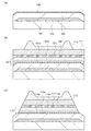
本実施の形態では、薄膜トランジスタの作製方法について、図1乃至図9を用いて示す。薄膜トランジスタは、p型よりもn型の方が、キャリアの移動度が高い。また、同一の基板上に形成する薄膜トランジスタを全て同じ極性に統一すると、工程数を抑えることができ、好ましい。そのため、本実施の形態では、n型の薄膜トランジスタの作製方法について説明する。
本実施の形態では、ゲート絶縁層105、第1の半導体層106、第2の半導体層107、及び不純物半導体層109の形成に用いることが可能なプラズマCVD装置の一形態について詳細に説明する。これらの層はCVD法等を用いて形成する。
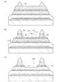
本実施の形態では、実施の形態1に適用可能な第2の半導体層107の形成工程について説明する。
本実施の形態では、実施の形態1に適用可能な第2の半導体層107の形成工程について説明する。
実施の形態1において、第2の半導体層107の作製方法について、図9を用いて示す。
実施の形態1とは異なる薄膜トランジスタの作製方法について、図10及び図11を用いて示す。
本実施の形態では、チャネル長が10μm以下と短い薄膜トランジスタにおいて、ソース領域及びドレイン領域の抵抗を低減することが可能な形態について、以下に示す。ここでは、実施の形態1を用いて説明するが、適宜他の実施の形態に適用可能である。
本実施の形態では、実施の形態1乃至実施の形態7で示す薄膜トランジスタを用いることが可能な、素子基板、及び当該素子基板を有する表示装置について、以下に示す。表示装置としては、液晶表示装置、発光表示装置、電子ペーパー等があるが、上記実施の形態の薄膜トランジスタは他の表示装置の素子基板にも用いることができる。ここでは、上記実施の形態1で示す薄膜トランジスタを有する液晶表示装置、代表的には、VA(Vertical Alignment)型の液晶表示装置について、図12及び図13を用いて説明する。
実施の形態8で示す素子基板313において、配向膜311を形成せず、発光素子を設けることにより、当該素子基板を発光表示装置や、発光装置に用いることができる。発光表示装置や発光装置は、発光素子として代表的には、エレクトロルミネッセンスを利用する発光素子がある。エレクトロルミネッセンスを利用する発光素子は、発光材料が有機化合物であるか、無機化合物であるかによって大別され、一般的に、前者は有機EL素子、後者は無機EL素子と呼ばれている。
上記実施の形態に係る薄膜トランジスタを有する表示装置は、さまざまな電子機器(遊技機も含む)に適用することができる。電子機器としては、例えば、テレビジョン装置(テレビ、またはテレビジョン受信機ともいう)、コンピュータ用などのモニタ、電子ペーパー、デジタルカメラやデジタルビデオカメラ等のカメラ、デジタルフォトフレーム、携帯電話機(携帯電話、携帯電話装置ともいう)、携帯型ゲーム機、携帯情報端末、音響再生装置、パチンコ機などの大型ゲーム機などが挙げられる。特に、実施の形態8及び実施の形態9で示したように、上記実施の形態に係る薄膜トランジスタを液晶表示装置、発光装置、電気泳動方式表示装置などに適用することにより、電子機器の表示部に用いることができる。以下に具体的に例示する。
Claims (3)
- 基板上のゲート電極と、
前記ゲート電極上のゲート絶縁層と、
前記ゲート絶縁層上の半導体層と、
前記半導体層上の不純物元素を含む半導体層と、
前記不純物元素を含む半導体層上のソース電極とドレイン電極とを有する薄膜トランジスタの作製方法であって、
前記半導体層は、前記ゲート絶縁層側から、第1の層と、前記第1の層上の第2の層と、前記第2の層上の第3の層とを有し、
前記第1の層は、微結晶半導体層であり、
前記第2の層は、微結晶半導体領域と、非晶質半導体領域とを有し、
前記第3の層は、非晶質半導体層であり、
前記第1の層は、前記ゲート絶縁層側の第1の領域と、前記第1の部分上の第2の領域とを有し、
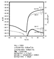
シリコンまたはゲルマニウムを含む堆積性気体と、水素と、希ガスとを混合し、シリコンまたはゲルマニウムを含む堆積性気体の流量に対して、水素の流量を10〜2000倍にし、高周波電力を印加することで、前記第1の領域を形成し、
前記第1の領域を形成後、シリコンまたはゲルマニウムを含む堆積性気体と、水素と、窒素を含む気体を混合し、シリコンまたはゲルマニウムを含む堆積性気体の流量に対して、水素の流量を10〜2000倍にし、高周波電力を印加することで、前記第2の領域と前記第2の層と前記第3の層とを形成することを特徴とする薄膜トランジスタの作製方法。 - 請求項1において、
前記第2の領域は、前記第1の領域を種結晶として結晶成長することで形成されることを特徴とする薄膜トランジスタの作製方法。 - 請求項1または請求項2において、
前記第2の層の前記微結晶半導体領域は、前記第1の層から前記第3の層に向かって、先端が狭まる凸状の領域であり、
前記第2の層の前記微結晶半導体領域以外は、前記非晶質半導体領域であることを特徴とする薄膜トランジスタの作製方法。
Priority Applications (1)
| Application Number | Priority Date | Filing Date | Title |
|---|---|---|---|
| JP2009257696A JP5498762B2 (ja) | 2008-11-17 | 2009-11-11 | 薄膜トランジスタの作製方法 |
Applications Claiming Priority (3)
| Application Number | Priority Date | Filing Date | Title |
|---|---|---|---|
| JP2008293954 | 2008-11-17 | ||
| JP2008293954 | 2008-11-17 | ||
| JP2009257696A JP5498762B2 (ja) | 2008-11-17 | 2009-11-11 | 薄膜トランジスタの作製方法 |
Publications (3)
| Publication Number | Publication Date |
|---|---|
| JP2010141306A JP2010141306A (ja) | 2010-06-24 |
| JP2010141306A5 JP2010141306A5 (ja) | 2012-12-20 |
| JP5498762B2 true JP5498762B2 (ja) | 2014-05-21 |
Family
ID=42172354
Family Applications (1)
| Application Number | Title | Priority Date | Filing Date |
|---|---|---|---|
| JP2009257696A Expired - Fee Related JP5498762B2 (ja) | 2008-11-17 | 2009-11-11 | 薄膜トランジスタの作製方法 |
Country Status (2)
| Country | Link |
|---|---|
| US (1) | US8569120B2 (ja) |
| JP (1) | JP5498762B2 (ja) |
Families Citing this family (8)
| Publication number | Priority date | Publication date | Assignee | Title |
|---|---|---|---|---|
| JP5525224B2 (ja) | 2008-09-30 | 2014-06-18 | 株式会社半導体エネルギー研究所 | 表示装置 |
| US8383434B2 (en) * | 2010-02-22 | 2013-02-26 | Semiconductor Energy Laboratory Co., Ltd. | Thin film transistor and manufacturing method thereof |
| TWI606490B (zh) | 2010-07-02 | 2017-11-21 | 半導體能源研究所股份有限公司 | 半導體膜的製造方法,半導體裝置的製造方法,和光電轉換裝置的製造方法 |
| JP5948025B2 (ja) * | 2010-08-06 | 2016-07-06 | 株式会社半導体エネルギー研究所 | 液晶表示装置 |
| JP5948040B2 (ja) | 2010-11-04 | 2016-07-06 | 株式会社半導体エネルギー研究所 | 結晶性半導体膜の作製方法及び半導体装置の作製方法 |
| US9048327B2 (en) * | 2011-01-25 | 2015-06-02 | Semiconductor Energy Laboratory Co., Ltd. | Microcrystalline semiconductor film, method for manufacturing the same, and method for manufacturing semiconductor device |
| JP6006948B2 (ja) * | 2011-03-17 | 2016-10-12 | 株式会社半導体エネルギー研究所 | 微結晶半導体膜、及び半導体装置の作製方法 |
| CN110797357A (zh) * | 2018-08-02 | 2020-02-14 | 夏普株式会社 | 摄像面板及其制造方法 |
Family Cites Families (54)
| Publication number | Priority date | Publication date | Assignee | Title |
|---|---|---|---|---|
| JPS56122123A (en) * | 1980-03-03 | 1981-09-25 | Shunpei Yamazaki | Semiamorphous semiconductor |
| US5091334A (en) * | 1980-03-03 | 1992-02-25 | Semiconductor Energy Laboratory Co., Ltd. | Semiconductor device |
| JPS5771126A (en) | 1980-10-21 | 1982-05-01 | Semiconductor Energy Lab Co Ltd | Semiamorhous semiconductor |
| JPS5892217A (ja) | 1981-11-28 | 1983-06-01 | Semiconductor Energy Lab Co Ltd | 半導体装置作製方法 |
| JPS5972781A (ja) | 1982-10-20 | 1984-04-24 | Semiconductor Energy Lab Co Ltd | 光電変換半導体装置 |
| JPS6027122A (ja) * | 1983-07-22 | 1985-02-12 | Semiconductor Energy Lab Co Ltd | 光プラズマ気相反応法 |
| JPS60160170A (ja) | 1984-01-31 | 1985-08-21 | Seiko Instr & Electronics Ltd | 薄膜トランジスタ |
| JPS62141776A (ja) * | 1985-12-17 | 1987-06-25 | Hitachi Ltd | 薄膜トランジスタ |
| US5221631A (en) * | 1989-02-17 | 1993-06-22 | International Business Machines Corporation | Method of fabricating a thin film transistor having a silicon carbide buffer layer |
| JP2839529B2 (ja) * | 1989-02-17 | 1998-12-16 | 株式会社東芝 | 薄膜トランジスタ |
| JPH03278466A (ja) * | 1990-03-27 | 1991-12-10 | Toshiba Corp | 薄膜トランジスタおよびその製造方法 |
| US7115902B1 (en) * | 1990-11-20 | 2006-10-03 | Semiconductor Energy Laboratory Co., Ltd. | Electro-optical device and method for manufacturing the same |
| US5514879A (en) * | 1990-11-20 | 1996-05-07 | Semiconductor Energy Laboratory Co., Ltd. | Gate insulated field effect transistors and method of manufacturing the same |
| KR950013784B1 (ko) * | 1990-11-20 | 1995-11-16 | 가부시키가이샤 한도오따이 에네루기 겐큐쇼 | 반도체 전계효과 트랜지스터 및 그 제조방법과 박막트랜지스터 |
| US5849601A (en) * | 1990-12-25 | 1998-12-15 | Semiconductor Energy Laboratory Co., Ltd. | Electro-optical device and method for manufacturing the same |
| US7098479B1 (en) * | 1990-12-25 | 2006-08-29 | Semiconductor Energy Laboratory Co., Ltd. | Electro-optical device and method for manufacturing the same |
| JPH04266019A (ja) | 1991-02-20 | 1992-09-22 | Canon Inc | 成膜方法 |
| JP3255942B2 (ja) * | 1991-06-19 | 2002-02-12 | 株式会社半導体エネルギー研究所 | 逆スタガ薄膜トランジスタの作製方法 |
| EP0535979A3 (en) | 1991-10-02 | 1993-07-21 | Sharp Kabushiki Kaisha | A thin film transistor and a method for producing the same |
| JPH05129608A (ja) | 1991-10-31 | 1993-05-25 | Sharp Corp | 半導体装置 |
| US6835523B1 (en) * | 1993-05-09 | 2004-12-28 | Semiconductor Energy Laboratory Co., Ltd. | Apparatus for fabricating coating and method of fabricating the coating |
| JPH06326312A (ja) | 1993-05-14 | 1994-11-25 | Toshiba Corp | アクティブマトリクス型表示装置 |
| US5932302A (en) * | 1993-07-20 | 1999-08-03 | Semiconductor Energy Laboratory Co., Ltd. | Method for fabricating with ultrasonic vibration a carbon coating |
| JPH07131030A (ja) * | 1993-11-05 | 1995-05-19 | Sony Corp | 表示用薄膜半導体装置及びその製造方法 |
| TW303526B (ja) * | 1994-12-27 | 1997-04-21 | Matsushita Electric Ind Co Ltd | |
| US5677236A (en) * | 1995-02-24 | 1997-10-14 | Mitsui Toatsu Chemicals, Inc. | Process for forming a thin microcrystalline silicon semiconductor film |
| US5920772A (en) * | 1997-06-27 | 1999-07-06 | Industrial Technology Research Institute | Method of fabricating a hybrid polysilicon/amorphous silicon TFT |
| JP2000277439A (ja) | 1999-03-25 | 2000-10-06 | Kanegafuchi Chem Ind Co Ltd | 結晶質シリコン系薄膜のプラズマcvd方法およびシリコン系薄膜光電変換装置の製造方法 |
| JP2001007024A (ja) | 1999-06-18 | 2001-01-12 | Sanyo Electric Co Ltd | 多結晶シリコン膜の形成方法 |
| JP2001053283A (ja) * | 1999-08-12 | 2001-02-23 | Semiconductor Energy Lab Co Ltd | 半導体装置及びその作製方法 |
| KR100436181B1 (ko) * | 2002-04-16 | 2004-06-12 | 엘지.필립스 엘시디 주식회사 | 액정표시장치용 어레이기판 제조방법 |
| JP2004014958A (ja) | 2002-06-11 | 2004-01-15 | Fuji Electric Holdings Co Ltd | 薄膜多結晶太陽電池とその製造方法 |
| WO2004086487A1 (ja) | 2003-03-26 | 2004-10-07 | Semiconductor Energy Laboratory Co. Ltd. | 半導体装置およびその作製方法 |
| JP4748954B2 (ja) | 2003-07-14 | 2011-08-17 | 株式会社半導体エネルギー研究所 | 液晶表示装置 |
| TWI368774B (en) * | 2003-07-14 | 2012-07-21 | Semiconductor Energy Lab | Light-emitting device |
| TWI336921B (en) * | 2003-07-18 | 2011-02-01 | Semiconductor Energy Lab | Method for manufacturing semiconductor device |
| US7211454B2 (en) * | 2003-07-25 | 2007-05-01 | Semiconductor Energy Laboratory Co., Ltd. | Manufacturing method of a light emitting device including moving the source of the vapor deposition parallel to the substrate |
| JP2005050905A (ja) * | 2003-07-30 | 2005-02-24 | Sharp Corp | シリコン薄膜太陽電池の製造方法 |
| JP5159021B2 (ja) | 2003-12-02 | 2013-03-06 | 株式会社半導体エネルギー研究所 | 半導体装置の作製方法 |
| TWI372463B (en) * | 2003-12-02 | 2012-09-11 | Semiconductor Energy Lab | Laser irradiation apparatus, laser irradiation method, and method for manufacturing semiconductor device |
| JP2005167051A (ja) | 2003-12-04 | 2005-06-23 | Sony Corp | 薄膜トランジスタおよび薄膜トランジスタの製造方法 |
| US7753751B2 (en) * | 2004-09-29 | 2010-07-13 | Semiconductor Energy Laboratory Co., Ltd. | Method of fabricating the display device |
| FR2893951B1 (fr) * | 2005-11-30 | 2008-02-29 | Centre Nat Rech Scient | Procede de production chez les procaryotes de transposases actives et stables d'elements genetiques mobiles mariner |
| JP2008124392A (ja) * | 2006-11-15 | 2008-05-29 | Sharp Corp | 半導体装置、その製造方法及び表示装置 |
| JP5331389B2 (ja) * | 2007-06-15 | 2013-10-30 | 株式会社半導体エネルギー研究所 | 表示装置の作製方法 |
| KR101635625B1 (ko) * | 2008-04-18 | 2016-07-01 | 가부시키가이샤 한도오따이 에네루기 켄큐쇼 | 박막 트랜지스터 및 그 제작 방법 |
| WO2009128522A1 (en) * | 2008-04-18 | 2009-10-22 | Semiconductor Energy Laboratory Co., Ltd. | Thin film transistor and method for manufacturing the same |
| JP5416460B2 (ja) * | 2008-04-18 | 2014-02-12 | 株式会社半導体エネルギー研究所 | 薄膜トランジスタおよび薄膜トランジスタの作製方法 |
| US8053294B2 (en) * | 2008-04-21 | 2011-11-08 | Semiconductor Energy Laboratory Co., Ltd. | Manufacturing method of thin film transistor by controlling generation of crystal nuclei of microcrystalline semiconductor film |
| US8049215B2 (en) * | 2008-04-25 | 2011-11-01 | Semiconductor Energy Laboratory Co., Ltd. | Thin film transistor |
| JP5436017B2 (ja) * | 2008-04-25 | 2014-03-05 | 株式会社半導体エネルギー研究所 | 半導体装置 |
| JP5518366B2 (ja) * | 2008-05-16 | 2014-06-11 | 株式会社半導体エネルギー研究所 | 薄膜トランジスタ |
| KR101703511B1 (ko) * | 2008-06-27 | 2017-02-07 | 가부시키가이샤 한도오따이 에네루기 켄큐쇼 | 박막 트랜지스터 |
| KR101602252B1 (ko) | 2008-06-27 | 2016-03-10 | 가부시키가이샤 한도오따이 에네루기 켄큐쇼 | 박막 트랜지스터, 반도체장치 및 전자기기 |
-
2009
- 2009-11-11 JP JP2009257696A patent/JP5498762B2/ja not_active Expired - Fee Related
- 2009-11-12 US US12/617,406 patent/US8569120B2/en not_active Expired - Fee Related
Also Published As
| Publication number | Publication date |
|---|---|
| JP2010141306A (ja) | 2010-06-24 |
| US8569120B2 (en) | 2013-10-29 |
| US20100124804A1 (en) | 2010-05-20 |
Similar Documents
| Publication | Publication Date | Title |
|---|---|---|
| JP5525215B2 (ja) | 半導体装置の作製方法 | |
| JP5506448B2 (ja) | 半導体装置 | |
| JP5498762B2 (ja) | 薄膜トランジスタの作製方法 | |
| JP5542277B2 (ja) | 微結晶半導体膜及び薄膜トランジスタの作製方法 | |
| US7989325B2 (en) | Method for manufacturing crystalline semiconductor film and method for manufacturing thin film transistor | |
| JP5542364B2 (ja) | 薄膜トランジスタの作製方法 | |
| US8956934B2 (en) | Thin film transistor and method for manufacturing the same | |
| JP5553703B2 (ja) | 半導体膜の作製方法および半導体装置の作製方法 | |
| JP5878603B2 (ja) | 半導体装置の作製方法 | |
| JP5495775B2 (ja) | 半導体装置 | |
| JP5490515B2 (ja) | 半導体装置 |
Legal Events
| Date | Code | Title | Description |
|---|---|---|---|
| A521 | Request for written amendment filed |
Free format text: JAPANESE INTERMEDIATE CODE: A523 Effective date: 20121101 |
|
| A621 | Written request for application examination |
Free format text: JAPANESE INTERMEDIATE CODE: A621 Effective date: 20121101 |
|
| A977 | Report on retrieval |
Free format text: JAPANESE INTERMEDIATE CODE: A971007 Effective date: 20131219 |
|
| A131 | Notification of reasons for refusal |
Free format text: JAPANESE INTERMEDIATE CODE: A131 Effective date: 20131224 |
|
| A521 | Request for written amendment filed |
Free format text: JAPANESE INTERMEDIATE CODE: A523 Effective date: 20140214 |
|
| TRDD | Decision of grant or rejection written | ||
| A01 | Written decision to grant a patent or to grant a registration (utility model) |
Free format text: JAPANESE INTERMEDIATE CODE: A01 Effective date: 20140304 |
|
| A61 | First payment of annual fees (during grant procedure) |
Free format text: JAPANESE INTERMEDIATE CODE: A61 Effective date: 20140310 |
|
| R150 | Certificate of patent or registration of utility model |
Ref document number: 5498762 Country of ref document: JP Free format text: JAPANESE INTERMEDIATE CODE: R150 |
|
| R250 | Receipt of annual fees |
Free format text: JAPANESE INTERMEDIATE CODE: R250 |
|
| R250 | Receipt of annual fees |
Free format text: JAPANESE INTERMEDIATE CODE: R250 |
|
| R250 | Receipt of annual fees |
Free format text: JAPANESE INTERMEDIATE CODE: R250 |
|
| R250 | Receipt of annual fees |
Free format text: JAPANESE INTERMEDIATE CODE: R250 |
|
| R250 | Receipt of annual fees |
Free format text: JAPANESE INTERMEDIATE CODE: R250 |
|
| LAPS | Cancellation because of no payment of annual fees |