JP5498762B2 - Method for manufacturing thin film transistor - Google Patents
Method for manufacturing thin film transistor Download PDFInfo
- Publication number
- JP5498762B2 JP5498762B2 JP2009257696A JP2009257696A JP5498762B2 JP 5498762 B2 JP5498762 B2 JP 5498762B2 JP 2009257696 A JP2009257696 A JP 2009257696A JP 2009257696 A JP2009257696 A JP 2009257696A JP 5498762 B2 JP5498762 B2 JP 5498762B2
- Authority
- JP
- Japan
- Prior art keywords
- layer
- semiconductor layer
- microcrystalline
- flow rate
- film transistor
- Prior art date
- Legal status (The legal status is an assumption and is not a legal conclusion. Google has not performed a legal analysis and makes no representation as to the accuracy of the status listed.)
- Expired - Fee Related
Links
- 239000010409 thin film Substances 0.000 title claims description 97
- 238000000034 method Methods 0.000 title claims description 75
- 238000004519 manufacturing process Methods 0.000 title claims description 29
- 239000004065 semiconductor Substances 0.000 claims description 488
- 239000007789 gas Substances 0.000 claims description 168
- IJGRMHOSHXDMSA-UHFFFAOYSA-N Atomic nitrogen Chemical compound N#N IJGRMHOSHXDMSA-UHFFFAOYSA-N 0.000 claims description 153
- 239000000758 substrate Substances 0.000 claims description 92
- 230000008021 deposition Effects 0.000 claims description 85
- 239000012535 impurity Substances 0.000 claims description 80
- 229910052757 nitrogen Inorganic materials 0.000 claims description 69
- 229910052710 silicon Inorganic materials 0.000 claims description 43
- XUIMIQQOPSSXEZ-UHFFFAOYSA-N Silicon Chemical compound [Si] XUIMIQQOPSSXEZ-UHFFFAOYSA-N 0.000 claims description 42
- 239000010703 silicon Substances 0.000 claims description 42
- 229910052739 hydrogen Inorganic materials 0.000 claims description 37
- 239000001257 hydrogen Substances 0.000 claims description 37
- 229910052732 germanium Inorganic materials 0.000 claims description 28
- GNPVGFCGXDBREM-UHFFFAOYSA-N germanium atom Chemical compound [Ge] GNPVGFCGXDBREM-UHFFFAOYSA-N 0.000 claims description 28
- 239000013078 crystal Substances 0.000 claims description 27
- UFHFLCQGNIYNRP-UHFFFAOYSA-N Hydrogen Chemical compound [H][H] UFHFLCQGNIYNRP-UHFFFAOYSA-N 0.000 claims description 21
- 150000002431 hydrogen Chemical class 0.000 claims description 18
- 239000010410 layer Substances 0.000 description 644
- XKRFYHLGVUSROY-UHFFFAOYSA-N Argon Chemical compound [Ar] XKRFYHLGVUSROY-UHFFFAOYSA-N 0.000 description 112
- 238000000151 deposition Methods 0.000 description 89
- 238000012545 processing Methods 0.000 description 71
- 229910052786 argon Inorganic materials 0.000 description 57
- 229910021424 microcrystalline silicon Inorganic materials 0.000 description 55
- QGZKDVFQNNGYKY-UHFFFAOYSA-N Ammonia Chemical compound N QGZKDVFQNNGYKY-UHFFFAOYSA-N 0.000 description 54
- 230000015572 biosynthetic process Effects 0.000 description 37
- 230000001965 increasing effect Effects 0.000 description 37
- 239000000463 material Substances 0.000 description 33
- 229910052581 Si3N4 Inorganic materials 0.000 description 28
- HQVNEWCFYHHQES-UHFFFAOYSA-N silicon nitride Chemical compound N12[Si]34N5[Si]62N3[Si]51N64 HQVNEWCFYHHQES-UHFFFAOYSA-N 0.000 description 28
- 229910021529 ammonia Inorganic materials 0.000 description 27
- 239000004973 liquid crystal related substance Substances 0.000 description 27
- 229910021417 amorphous silicon Inorganic materials 0.000 description 24
- 238000005268 plasma chemical vapour deposition Methods 0.000 description 18
- BLRPTPMANUNPDV-UHFFFAOYSA-N Silane Chemical compound [SiH4] BLRPTPMANUNPDV-UHFFFAOYSA-N 0.000 description 17
- 239000010408 film Substances 0.000 description 17
- 229910000077 silane Inorganic materials 0.000 description 17
- 238000005530 etching Methods 0.000 description 16
- 229910001873 dinitrogen Inorganic materials 0.000 description 15
- 230000006870 function Effects 0.000 description 13
- QVGXLLKOCUKJST-UHFFFAOYSA-N atomic oxygen Chemical compound [O] QVGXLLKOCUKJST-UHFFFAOYSA-N 0.000 description 11
- 230000005669 field effect Effects 0.000 description 11
- 239000011521 glass Substances 0.000 description 11
- 239000001301 oxygen Substances 0.000 description 11
- 229910052760 oxygen Inorganic materials 0.000 description 11
- ZOKXTWBITQBERF-UHFFFAOYSA-N Molybdenum Chemical compound [Mo] ZOKXTWBITQBERF-UHFFFAOYSA-N 0.000 description 10
- OAICVXFJPJFONN-UHFFFAOYSA-N Phosphorus Chemical compound [P] OAICVXFJPJFONN-UHFFFAOYSA-N 0.000 description 10
- 239000003990 capacitor Substances 0.000 description 10
- 229910052734 helium Inorganic materials 0.000 description 10
- 239000001307 helium Substances 0.000 description 10
- SWQJXJOGLNCZEY-UHFFFAOYSA-N helium atom Chemical compound [He] SWQJXJOGLNCZEY-UHFFFAOYSA-N 0.000 description 10
- 229910052743 krypton Inorganic materials 0.000 description 10
- DNNSSWSSYDEUBZ-UHFFFAOYSA-N krypton atom Chemical compound [Kr] DNNSSWSSYDEUBZ-UHFFFAOYSA-N 0.000 description 10
- 229910052750 molybdenum Inorganic materials 0.000 description 10
- 239000011733 molybdenum Substances 0.000 description 10
- 229910052754 neon Inorganic materials 0.000 description 10
- GKAOGPIIYCISHV-UHFFFAOYSA-N neon atom Chemical compound [Ne] GKAOGPIIYCISHV-UHFFFAOYSA-N 0.000 description 10
- 229910052698 phosphorus Inorganic materials 0.000 description 10
- 239000011574 phosphorus Substances 0.000 description 10
- 229910052724 xenon Inorganic materials 0.000 description 9
- FHNFHKCVQCLJFQ-UHFFFAOYSA-N xenon atom Chemical compound [Xe] FHNFHKCVQCLJFQ-UHFFFAOYSA-N 0.000 description 9
- 238000001069 Raman spectroscopy Methods 0.000 description 8
- 238000004040 coloring Methods 0.000 description 8
- 230000007547 defect Effects 0.000 description 8
- 229910052814 silicon oxide Inorganic materials 0.000 description 8
- VYPSYNLAJGMNEJ-UHFFFAOYSA-N Silicium dioxide Chemical compound O=[Si]=O VYPSYNLAJGMNEJ-UHFFFAOYSA-N 0.000 description 7
- 238000010790 dilution Methods 0.000 description 6
- 239000012895 dilution Substances 0.000 description 6
- 238000009616 inductively coupled plasma Methods 0.000 description 6
- XLYOFNOQVPJJNP-UHFFFAOYSA-N water Substances O XLYOFNOQVPJJNP-UHFFFAOYSA-N 0.000 description 6
- 238000001237 Raman spectrum Methods 0.000 description 5
- 229910052782 aluminium Inorganic materials 0.000 description 5
- XAGFODPZIPBFFR-UHFFFAOYSA-N aluminium Chemical compound [Al] XAGFODPZIPBFFR-UHFFFAOYSA-N 0.000 description 5
- 239000000460 chlorine Substances 0.000 description 5
- 238000001312 dry etching Methods 0.000 description 5
- 229910021420 polycrystalline silicon Inorganic materials 0.000 description 5
- 239000011241 protective layer Substances 0.000 description 5
- 238000001004 secondary ion mass spectrometry Methods 0.000 description 5
- 238000004611 spectroscopical analysis Methods 0.000 description 5
- 238000002834 transmittance Methods 0.000 description 5
- ZAMOUSCENKQFHK-UHFFFAOYSA-N Chlorine atom Chemical compound [Cl] ZAMOUSCENKQFHK-UHFFFAOYSA-N 0.000 description 4
- VYZAMTAEIAYCRO-UHFFFAOYSA-N Chromium Chemical compound [Cr] VYZAMTAEIAYCRO-UHFFFAOYSA-N 0.000 description 4
- RYGMFSIKBFXOCR-UHFFFAOYSA-N Copper Chemical compound [Cu] RYGMFSIKBFXOCR-UHFFFAOYSA-N 0.000 description 4
- XYFCBTPGUUZFHI-UHFFFAOYSA-N Phosphine Chemical compound P XYFCBTPGUUZFHI-UHFFFAOYSA-N 0.000 description 4
- BOTDANWDWHJENH-UHFFFAOYSA-N Tetraethyl orthosilicate Chemical compound CCO[Si](OCC)(OCC)OCC BOTDANWDWHJENH-UHFFFAOYSA-N 0.000 description 4
- RTAQQCXQSZGOHL-UHFFFAOYSA-N Titanium Chemical compound [Ti] RTAQQCXQSZGOHL-UHFFFAOYSA-N 0.000 description 4
- LEVVHYCKPQWKOP-UHFFFAOYSA-N [Si].[Ge] Chemical compound [Si].[Ge] LEVVHYCKPQWKOP-UHFFFAOYSA-N 0.000 description 4
- 238000005229 chemical vapour deposition Methods 0.000 description 4
- 229910052801 chlorine Inorganic materials 0.000 description 4
- 229910052804 chromium Inorganic materials 0.000 description 4
- 239000011651 chromium Substances 0.000 description 4
- 238000004140 cleaning Methods 0.000 description 4
- 229910052802 copper Inorganic materials 0.000 description 4
- 239000010949 copper Substances 0.000 description 4
- 238000011161 development Methods 0.000 description 4
- 238000005259 measurement Methods 0.000 description 4
- 229910021421 monocrystalline silicon Inorganic materials 0.000 description 4
- 238000009832 plasma treatment Methods 0.000 description 4
- 239000012495 reaction gas Substances 0.000 description 4
- 238000004544 sputter deposition Methods 0.000 description 4
- 229910052715 tantalum Inorganic materials 0.000 description 4
- GUVRBAGPIYLISA-UHFFFAOYSA-N tantalum atom Chemical compound [Ta] GUVRBAGPIYLISA-UHFFFAOYSA-N 0.000 description 4
- 229910052719 titanium Inorganic materials 0.000 description 4
- 239000010936 titanium Substances 0.000 description 4
- WFKWXMTUELFFGS-UHFFFAOYSA-N tungsten Chemical compound [W] WFKWXMTUELFFGS-UHFFFAOYSA-N 0.000 description 4
- 229910052721 tungsten Inorganic materials 0.000 description 4
- 239000010937 tungsten Substances 0.000 description 4
- 229910000838 Al alloy Inorganic materials 0.000 description 3
- 239000000956 alloy Substances 0.000 description 3
- 238000006243 chemical reaction Methods 0.000 description 3
- 230000007423 decrease Effects 0.000 description 3
- 238000003780 insertion Methods 0.000 description 3
- 230000037431 insertion Effects 0.000 description 3
- 229910052751 metal Inorganic materials 0.000 description 3
- 239000002184 metal Substances 0.000 description 3
- 239000013081 microcrystal Substances 0.000 description 3
- 238000002156 mixing Methods 0.000 description 3
- 150000004767 nitrides Chemical class 0.000 description 3
- QJGQUHMNIGDVPM-UHFFFAOYSA-N nitrogen group Chemical group [N] QJGQUHMNIGDVPM-UHFFFAOYSA-N 0.000 description 3
- -1 preferably NH groups Substances 0.000 description 3
- 238000007639 printing Methods 0.000 description 3
- 239000002356 single layer Substances 0.000 description 3
- 239000000126 substance Substances 0.000 description 3
- 238000001039 wet etching Methods 0.000 description 3
- WZJUBBHODHNQPW-UHFFFAOYSA-N 2,4,6,8-tetramethyl-1,3,5,7,2$l^{3},4$l^{3},6$l^{3},8$l^{3}-tetraoxatetrasilocane Chemical compound C[Si]1O[Si](C)O[Si](C)O[Si](C)O1 WZJUBBHODHNQPW-UHFFFAOYSA-N 0.000 description 2
- 229910052779 Neodymium Inorganic materials 0.000 description 2
- BQCADISMDOOEFD-UHFFFAOYSA-N Silver Chemical compound [Ag] BQCADISMDOOEFD-UHFFFAOYSA-N 0.000 description 2
- WGLPBDUCMAPZCE-UHFFFAOYSA-N Trioxochromium Chemical compound O=[Cr](=O)=O WGLPBDUCMAPZCE-UHFFFAOYSA-N 0.000 description 2
- 229910045601 alloy Inorganic materials 0.000 description 2
- 238000004380 ashing Methods 0.000 description 2
- 239000000969 carrier Substances 0.000 description 2
- 230000001413 cellular effect Effects 0.000 description 2
- 229910000423 chromium oxide Inorganic materials 0.000 description 2
- 238000000576 coating method Methods 0.000 description 2
- 238000004891 communication Methods 0.000 description 2
- 230000008878 coupling Effects 0.000 description 2
- 238000010168 coupling process Methods 0.000 description 2
- 238000005859 coupling reaction Methods 0.000 description 2
- 229910021419 crystalline silicon Inorganic materials 0.000 description 2
- 238000013461 design Methods 0.000 description 2
- 238000001514 detection method Methods 0.000 description 2
- 238000007599 discharging Methods 0.000 description 2
- 238000010494 dissociation reaction Methods 0.000 description 2
- 230000005593 dissociations Effects 0.000 description 2
- 230000000694 effects Effects 0.000 description 2
- 238000005401 electroluminescence Methods 0.000 description 2
- 238000005868 electrolysis reaction Methods 0.000 description 2
- 230000002349 favourable effect Effects 0.000 description 2
- PCHJSUWPFVWCPO-UHFFFAOYSA-N gold Chemical compound [Au] PCHJSUWPFVWCPO-UHFFFAOYSA-N 0.000 description 2
- 229910052737 gold Inorganic materials 0.000 description 2
- 239000010931 gold Substances 0.000 description 2
- 239000007769 metal material Substances 0.000 description 2
- QEFYFXOXNSNQGX-UHFFFAOYSA-N neodymium atom Chemical compound [Nd] QEFYFXOXNSNQGX-UHFFFAOYSA-N 0.000 description 2
- QEHKBHWEUPXBCW-UHFFFAOYSA-N nitrogen trichloride Chemical compound ClN(Cl)Cl QEHKBHWEUPXBCW-UHFFFAOYSA-N 0.000 description 2
- GVGCUCJTUSOZKP-UHFFFAOYSA-N nitrogen trifluoride Chemical compound FN(F)F GVGCUCJTUSOZKP-UHFFFAOYSA-N 0.000 description 2
- HMMGMWAXVFQUOA-UHFFFAOYSA-N octamethylcyclotetrasiloxane Chemical compound C[Si]1(C)O[Si](C)(C)O[Si](C)(C)O[Si](C)(C)O1 HMMGMWAXVFQUOA-UHFFFAOYSA-N 0.000 description 2
- 230000003287 optical effect Effects 0.000 description 2
- 230000000737 periodic effect Effects 0.000 description 2
- 229910000073 phosphorus hydride Inorganic materials 0.000 description 2
- 238000000206 photolithography Methods 0.000 description 2
- 238000001020 plasma etching Methods 0.000 description 2
- 239000011148 porous material Substances 0.000 description 2
- 239000002994 raw material Substances 0.000 description 2
- 229910052706 scandium Inorganic materials 0.000 description 2
- SIXSYDAISGFNSX-UHFFFAOYSA-N scandium atom Chemical compound [Sc] SIXSYDAISGFNSX-UHFFFAOYSA-N 0.000 description 2
- 239000000565 sealant Substances 0.000 description 2
- 229910052709 silver Inorganic materials 0.000 description 2
- 239000004332 silver Substances 0.000 description 2
- TXEYQDLBPFQVAA-UHFFFAOYSA-N tetrafluoromethane Chemical compound FC(F)(F)F TXEYQDLBPFQVAA-UHFFFAOYSA-N 0.000 description 2
- CZDYPVPMEAXLPK-UHFFFAOYSA-N tetramethylsilane Chemical compound C[Si](C)(C)C CZDYPVPMEAXLPK-UHFFFAOYSA-N 0.000 description 2
- 238000001771 vacuum deposition Methods 0.000 description 2
- 210000003462 vein Anatomy 0.000 description 2
- ZOXJGFHDIHLPTG-UHFFFAOYSA-N Boron Chemical compound [B] ZOXJGFHDIHLPTG-UHFFFAOYSA-N 0.000 description 1
- 229910019974 CrSi Inorganic materials 0.000 description 1
- 229910016006 MoSi Inorganic materials 0.000 description 1
- 229910000583 Nd alloy Inorganic materials 0.000 description 1
- NRTOMJZYCJJWKI-UHFFFAOYSA-N Titanium nitride Chemical compound [Ti]#N NRTOMJZYCJJWKI-UHFFFAOYSA-N 0.000 description 1
- 230000001133 acceleration Effects 0.000 description 1
- 239000005407 aluminoborosilicate glass Substances 0.000 description 1
- 239000005354 aluminosilicate glass Substances 0.000 description 1
- UBSJOWMHLJZVDJ-UHFFFAOYSA-N aluminum neodymium Chemical compound [Al].[Nd] UBSJOWMHLJZVDJ-UHFFFAOYSA-N 0.000 description 1
- 238000013459 approach Methods 0.000 description 1
- 125000004429 atom Chemical group 0.000 description 1
- 229910052788 barium Inorganic materials 0.000 description 1
- DSAJWYNOEDNPEQ-UHFFFAOYSA-N barium atom Chemical compound [Ba] DSAJWYNOEDNPEQ-UHFFFAOYSA-N 0.000 description 1
- 230000002457 bidirectional effect Effects 0.000 description 1
- 229910052796 boron Inorganic materials 0.000 description 1
- 239000005388 borosilicate glass Substances 0.000 description 1
- 230000015556 catabolic process Effects 0.000 description 1
- 239000000919 ceramic Substances 0.000 description 1
- 239000011248 coating agent Substances 0.000 description 1
- 238000002425 crystallisation Methods 0.000 description 1
- 230000008025 crystallization Effects 0.000 description 1
- 230000000994 depressogenic effect Effects 0.000 description 1
- 238000007865 diluting Methods 0.000 description 1
- 238000006073 displacement reaction Methods 0.000 description 1
- OYFJQPXVCSSHAI-QFPUQLAESA-N enalapril maleate Chemical compound OC(=O)\C=C/C(O)=O.C([C@@H](C(=O)OCC)N[C@@H](C)C(=O)N1[C@@H](CCC1)C(O)=O)CC1=CC=CC=C1 OYFJQPXVCSSHAI-QFPUQLAESA-N 0.000 description 1
- 238000005516 engineering process Methods 0.000 description 1
- 238000011049 filling Methods 0.000 description 1
- NBVXSUQYWXRMNV-UHFFFAOYSA-N fluoromethane Chemical compound FC NBVXSUQYWXRMNV-UHFFFAOYSA-N 0.000 description 1
- 239000008187 granular material Substances 0.000 description 1
- 229910052736 halogen Inorganic materials 0.000 description 1
- 150000002367 halogens Chemical class 0.000 description 1
- 238000010438 heat treatment Methods 0.000 description 1
- FFUAGWLWBBFQJT-UHFFFAOYSA-N hexamethyldisilazane Chemical compound C[Si](C)(C)N[Si](C)(C)C FFUAGWLWBBFQJT-UHFFFAOYSA-N 0.000 description 1
- 230000001939 inductive effect Effects 0.000 description 1
- 150000002484 inorganic compounds Chemical class 0.000 description 1
- 229910010272 inorganic material Inorganic materials 0.000 description 1
- 238000009413 insulation Methods 0.000 description 1
- 150000002500 ions Chemical class 0.000 description 1
- 238000005224 laser annealing Methods 0.000 description 1
- 150000002894 organic compounds Chemical class 0.000 description 1
- 150000001282 organosilanes Chemical class 0.000 description 1
- 238000005424 photoluminescence Methods 0.000 description 1
- 230000002265 prevention Effects 0.000 description 1
- 230000001681 protective effect Effects 0.000 description 1
- 239000010453 quartz Substances 0.000 description 1
- 238000007650 screen-printing Methods 0.000 description 1
- 239000002210 silicon-based material Substances 0.000 description 1
- 125000006850 spacer group Chemical group 0.000 description 1
- 238000003860 storage Methods 0.000 description 1
- 238000010896 thin film analysis Methods 0.000 description 1
- QQQSFSZALRVCSZ-UHFFFAOYSA-N triethoxysilane Chemical compound CCO[SiH](OCC)OCC QQQSFSZALRVCSZ-UHFFFAOYSA-N 0.000 description 1
Images


Classifications
-
- H—ELECTRICITY
- H01—ELECTRIC ELEMENTS
- H01L—SEMICONDUCTOR DEVICES NOT COVERED BY CLASS H10
- H01L27/00—Devices consisting of a plurality of semiconductor or other solid-state components formed in or on a common substrate
- H01L27/02—Devices consisting of a plurality of semiconductor or other solid-state components formed in or on a common substrate including semiconductor components specially adapted for rectifying, oscillating, amplifying or switching and having potential barriers; including integrated passive circuit elements having potential barriers
- H01L27/12—Devices consisting of a plurality of semiconductor or other solid-state components formed in or on a common substrate including semiconductor components specially adapted for rectifying, oscillating, amplifying or switching and having potential barriers; including integrated passive circuit elements having potential barriers the substrate being other than a semiconductor body, e.g. an insulating body
- H01L27/1214—Devices consisting of a plurality of semiconductor or other solid-state components formed in or on a common substrate including semiconductor components specially adapted for rectifying, oscillating, amplifying or switching and having potential barriers; including integrated passive circuit elements having potential barriers the substrate being other than a semiconductor body, e.g. an insulating body comprising a plurality of TFTs formed on a non-semiconducting substrate, e.g. driving circuits for AMLCDs
- H01L27/1259—Multistep manufacturing methods
- H01L27/1288—Multistep manufacturing methods employing particular masking sequences or specially adapted masks, e.g. half-tone mask
-
- C—CHEMISTRY; METALLURGY
- C23—COATING METALLIC MATERIAL; COATING MATERIAL WITH METALLIC MATERIAL; CHEMICAL SURFACE TREATMENT; DIFFUSION TREATMENT OF METALLIC MATERIAL; COATING BY VACUUM EVAPORATION, BY SPUTTERING, BY ION IMPLANTATION OR BY CHEMICAL VAPOUR DEPOSITION, IN GENERAL; INHIBITING CORROSION OF METALLIC MATERIAL OR INCRUSTATION IN GENERAL
- C23C—COATING METALLIC MATERIAL; COATING MATERIAL WITH METALLIC MATERIAL; SURFACE TREATMENT OF METALLIC MATERIAL BY DIFFUSION INTO THE SURFACE, BY CHEMICAL CONVERSION OR SUBSTITUTION; COATING BY VACUUM EVAPORATION, BY SPUTTERING, BY ION IMPLANTATION OR BY CHEMICAL VAPOUR DEPOSITION, IN GENERAL
- C23C16/00—Chemical coating by decomposition of gaseous compounds, without leaving reaction products of surface material in the coating, i.e. chemical vapour deposition [CVD] processes
- C23C16/02—Pretreatment of the material to be coated
- C23C16/0272—Deposition of sub-layers, e.g. to promote the adhesion of the main coating
-
- C—CHEMISTRY; METALLURGY
- C23—COATING METALLIC MATERIAL; COATING MATERIAL WITH METALLIC MATERIAL; CHEMICAL SURFACE TREATMENT; DIFFUSION TREATMENT OF METALLIC MATERIAL; COATING BY VACUUM EVAPORATION, BY SPUTTERING, BY ION IMPLANTATION OR BY CHEMICAL VAPOUR DEPOSITION, IN GENERAL; INHIBITING CORROSION OF METALLIC MATERIAL OR INCRUSTATION IN GENERAL
- C23C—COATING METALLIC MATERIAL; COATING MATERIAL WITH METALLIC MATERIAL; SURFACE TREATMENT OF METALLIC MATERIAL BY DIFFUSION INTO THE SURFACE, BY CHEMICAL CONVERSION OR SUBSTITUTION; COATING BY VACUUM EVAPORATION, BY SPUTTERING, BY ION IMPLANTATION OR BY CHEMICAL VAPOUR DEPOSITION, IN GENERAL
- C23C16/00—Chemical coating by decomposition of gaseous compounds, without leaving reaction products of surface material in the coating, i.e. chemical vapour deposition [CVD] processes
- C23C16/22—Chemical coating by decomposition of gaseous compounds, without leaving reaction products of surface material in the coating, i.e. chemical vapour deposition [CVD] processes characterised by the deposition of inorganic material, other than metallic material
- C23C16/24—Deposition of silicon only
-
- C—CHEMISTRY; METALLURGY
- C23—COATING METALLIC MATERIAL; COATING MATERIAL WITH METALLIC MATERIAL; CHEMICAL SURFACE TREATMENT; DIFFUSION TREATMENT OF METALLIC MATERIAL; COATING BY VACUUM EVAPORATION, BY SPUTTERING, BY ION IMPLANTATION OR BY CHEMICAL VAPOUR DEPOSITION, IN GENERAL; INHIBITING CORROSION OF METALLIC MATERIAL OR INCRUSTATION IN GENERAL
- C23C—COATING METALLIC MATERIAL; COATING MATERIAL WITH METALLIC MATERIAL; SURFACE TREATMENT OF METALLIC MATERIAL BY DIFFUSION INTO THE SURFACE, BY CHEMICAL CONVERSION OR SUBSTITUTION; COATING BY VACUUM EVAPORATION, BY SPUTTERING, BY ION IMPLANTATION OR BY CHEMICAL VAPOUR DEPOSITION, IN GENERAL
- C23C16/00—Chemical coating by decomposition of gaseous compounds, without leaving reaction products of surface material in the coating, i.e. chemical vapour deposition [CVD] processes
- C23C16/44—Chemical coating by decomposition of gaseous compounds, without leaving reaction products of surface material in the coating, i.e. chemical vapour deposition [CVD] processes characterised by the method of coating
- C23C16/50—Chemical coating by decomposition of gaseous compounds, without leaving reaction products of surface material in the coating, i.e. chemical vapour deposition [CVD] processes characterised by the method of coating using electric discharges
-
- H—ELECTRICITY
- H01—ELECTRIC ELEMENTS
- H01L—SEMICONDUCTOR DEVICES NOT COVERED BY CLASS H10
- H01L27/00—Devices consisting of a plurality of semiconductor or other solid-state components formed in or on a common substrate
- H01L27/02—Devices consisting of a plurality of semiconductor or other solid-state components formed in or on a common substrate including semiconductor components specially adapted for rectifying, oscillating, amplifying or switching and having potential barriers; including integrated passive circuit elements having potential barriers
- H01L27/12—Devices consisting of a plurality of semiconductor or other solid-state components formed in or on a common substrate including semiconductor components specially adapted for rectifying, oscillating, amplifying or switching and having potential barriers; including integrated passive circuit elements having potential barriers the substrate being other than a semiconductor body, e.g. an insulating body
- H01L27/1214—Devices consisting of a plurality of semiconductor or other solid-state components formed in or on a common substrate including semiconductor components specially adapted for rectifying, oscillating, amplifying or switching and having potential barriers; including integrated passive circuit elements having potential barriers the substrate being other than a semiconductor body, e.g. an insulating body comprising a plurality of TFTs formed on a non-semiconducting substrate, e.g. driving circuits for AMLCDs
-
- H—ELECTRICITY
- H01—ELECTRIC ELEMENTS
- H01L—SEMICONDUCTOR DEVICES NOT COVERED BY CLASS H10
- H01L29/00—Semiconductor devices specially adapted for rectifying, amplifying, oscillating or switching and having potential barriers; Capacitors or resistors having potential barriers, e.g. a PN-junction depletion layer or carrier concentration layer; Details of semiconductor bodies or of electrodes thereof ; Multistep manufacturing processes therefor
- H01L29/66—Types of semiconductor device ; Multistep manufacturing processes therefor
- H01L29/66007—Multistep manufacturing processes
- H01L29/66075—Multistep manufacturing processes of devices having semiconductor bodies comprising group 14 or group 13/15 materials
- H01L29/66227—Multistep manufacturing processes of devices having semiconductor bodies comprising group 14 or group 13/15 materials the devices being controllable only by the electric current supplied or the electric potential applied, to an electrode which does not carry the current to be rectified, amplified or switched, e.g. three-terminal devices
- H01L29/66409—Unipolar field-effect transistors
- H01L29/66477—Unipolar field-effect transistors with an insulated gate, i.e. MISFET
- H01L29/66742—Thin film unipolar transistors
- H01L29/6675—Amorphous silicon or polysilicon transistors
- H01L29/66765—Lateral single gate single channel transistors with inverted structure, i.e. the channel layer is formed after the gate
-
- H—ELECTRICITY
- H01—ELECTRIC ELEMENTS
- H01L—SEMICONDUCTOR DEVICES NOT COVERED BY CLASS H10
- H01L29/00—Semiconductor devices specially adapted for rectifying, amplifying, oscillating or switching and having potential barriers; Capacitors or resistors having potential barriers, e.g. a PN-junction depletion layer or carrier concentration layer; Details of semiconductor bodies or of electrodes thereof ; Multistep manufacturing processes therefor
- H01L29/66—Types of semiconductor device ; Multistep manufacturing processes therefor
- H01L29/68—Types of semiconductor device ; Multistep manufacturing processes therefor controllable by only the electric current supplied, or only the electric potential applied, to an electrode which does not carry the current to be rectified, amplified or switched
- H01L29/76—Unipolar devices, e.g. field effect transistors
- H01L29/772—Field effect transistors
- H01L29/78—Field effect transistors with field effect produced by an insulated gate
- H01L29/786—Thin film transistors, i.e. transistors with a channel being at least partly a thin film
- H01L29/78651—Silicon transistors
- H01L29/7866—Non-monocrystalline silicon transistors
- H01L29/78663—Amorphous silicon transistors
- H01L29/78669—Amorphous silicon transistors with inverted-type structure, e.g. with bottom gate
-
- H—ELECTRICITY
- H01—ELECTRIC ELEMENTS
- H01L—SEMICONDUCTOR DEVICES NOT COVERED BY CLASS H10
- H01L29/00—Semiconductor devices specially adapted for rectifying, amplifying, oscillating or switching and having potential barriers; Capacitors or resistors having potential barriers, e.g. a PN-junction depletion layer or carrier concentration layer; Details of semiconductor bodies or of electrodes thereof ; Multistep manufacturing processes therefor
- H01L29/66—Types of semiconductor device ; Multistep manufacturing processes therefor
- H01L29/68—Types of semiconductor device ; Multistep manufacturing processes therefor controllable by only the electric current supplied, or only the electric potential applied, to an electrode which does not carry the current to be rectified, amplified or switched
- H01L29/76—Unipolar devices, e.g. field effect transistors
- H01L29/772—Field effect transistors
- H01L29/78—Field effect transistors with field effect produced by an insulated gate
- H01L29/786—Thin film transistors, i.e. transistors with a channel being at least partly a thin film
- H01L29/78651—Silicon transistors
- H01L29/7866—Non-monocrystalline silicon transistors
- H01L29/78672—Polycrystalline or microcrystalline silicon transistor
- H01L29/78678—Polycrystalline or microcrystalline silicon transistor with inverted-type structure, e.g. with bottom gate
Landscapes
- Engineering & Computer Science (AREA)
- Chemical & Material Sciences (AREA)
- Power Engineering (AREA)
- Microelectronics & Electronic Packaging (AREA)
- Physics & Mathematics (AREA)
- Condensed Matter Physics & Semiconductors (AREA)
- General Physics & Mathematics (AREA)
- Computer Hardware Design (AREA)
- General Chemical & Material Sciences (AREA)
- Organic Chemistry (AREA)
- Ceramic Engineering (AREA)
- Chemical Kinetics & Catalysis (AREA)
- Materials Engineering (AREA)
- Mechanical Engineering (AREA)
- Metallurgy (AREA)
- Manufacturing & Machinery (AREA)
- Inorganic Chemistry (AREA)
- Crystallography & Structural Chemistry (AREA)
- Plasma & Fusion (AREA)
- Liquid Crystal (AREA)
- Thin Film Transistor (AREA)
- Formation Of Insulating Films (AREA)
- Recrystallisation Techniques (AREA)
Description
本発明は、薄膜トランジスタの作製方法、及び該薄膜トランジスタを用いた表示装置に関する。 The present invention relates to a method for manufacturing a thin film transistor and a display device using the thin film transistor.
電界効果トランジスタの一種として、絶縁表面を有する基板上に形成された半導体層にチャネル領域が形成される薄膜トランジスタが知られている。薄膜トランジスタに用いられる半導体層として、非晶質シリコン、微結晶シリコン及び多結晶シリコンを用いる技術が開示されている(特許文献1乃至5参照)。薄膜トランジスタの代表的な応用例は、液晶テレビジョン装置であり、表示画面を構成する各画素のスイッチングトランジスタとして実用化されている。
As a kind of field effect transistor, a thin film transistor in which a channel region is formed in a semiconductor layer formed over a substrate having an insulating surface is known. A technique using amorphous silicon, microcrystalline silicon, or polycrystalline silicon as a semiconductor layer used in a thin film transistor is disclosed (see
非晶質シリコン層を用いてチャネルが形成される薄膜トランジスタは、電界効果移動度及びオン電流が低いといった問題がある。一方、微結晶シリコン層にチャネルが形成される薄膜トランジスタは、非晶質シリコンでチャネルが形成される薄膜トランジスタと比較して、電界効果移動度が向上するもののオフ電流が高くなってしまい、十分なスイッチング特性が得られないといった問題がある。 A thin film transistor in which a channel is formed using an amorphous silicon layer has a problem that field-effect mobility and on-state current are low. On the other hand, a thin film transistor in which a channel is formed in a microcrystalline silicon layer improves field effect mobility but has a higher off-state current than a thin film transistor in which a channel is formed of amorphous silicon, and thus has sufficient switching. There is a problem that characteristics cannot be obtained.
多結晶シリコン層がチャネル形成領域となる薄膜トランジスタは、上記二種類の薄膜トランジスタよりも電界効果移動度が格段に高く、高いオン電流が得られるといった特性がある。この薄膜トランジスタは、前記した特性により、画素に設けられるスイッチング用のトランジスタのみならず、高速動作が要求されるドライバ回路をも構成することができる。 A thin film transistor in which a polycrystalline silicon layer serves as a channel formation region has characteristics that field effect mobility is significantly higher than that of the two types of thin film transistors, and a high on-state current can be obtained. Due to the above-described characteristics, this thin film transistor can constitute not only a switching transistor provided in a pixel but also a driver circuit that requires high-speed operation.
しかし、多結晶シリコン層により薄膜トランジスタは、非晶質シリコン層で薄膜トランジスタを形成する場合に比べ半導体層の結晶化工程が必要となり、製造コストが増大することが問題となっている。例えば、多結晶シリコン層の製造のために必要なレーザアニール技術は、レーザビームの照射面積が小さく大画面の液晶パネルを効率良く生産することができないといった問題がある。 However, a thin film transistor using a polycrystalline silicon layer requires a crystallization process of a semiconductor layer as compared with a case where a thin film transistor is formed using an amorphous silicon layer, which increases the manufacturing cost. For example, a laser annealing technique necessary for manufacturing a polycrystalline silicon layer has a problem that a large area liquid crystal panel cannot be efficiently produced with a small laser beam irradiation area.
ところで、表示パネルの製造に用いられているガラス基板は、第3世代(550mm×650mm)、第3.5世代(600mm×720mm、または620mm×750mm)、第4世代(680mm×880mm、または730mm×920mm)、第5世代(1100mm×1300mm)、第6世代(1500mm×1850mm)、第7世代(1870mm×2200mm)、第8世代(2200mm×2400mm)と年々大型化が進んでおり、今後は第9世代(2400mm×2800mm、2450mm×3050mm)、第10世代(2950mm×3400mm)へと大面積化が進むと予測されている。ガラス基板の大型化はコストミニマム設計の思想に基づいている。 By the way, the glass substrate used for manufacturing the display panel is the third generation (550 mm × 650 mm), the 3.5th generation (600 mm × 720 mm, or 620 mm × 750 mm), the fourth generation (680 mm × 880 mm, or 730 mm). × 920mm), 5th generation (1100mm × 1300mm), 6th generation (1500mm × 1850mm), 7th generation (1870mm × 2200mm), 8th generation (2200mm × 2400mm) It is predicted that the area will increase toward the ninth generation (2400 mm × 2800 mm, 2450 mm × 3050 mm) and the tenth generation (2950 mm × 3400 mm). The increase in size of the glass substrate is based on the idea of cost minimum design.
これに対して、第10世代(2950mm×3400mm)におけるような大面積のマザーガラス基板に、高速動作が可能な薄膜トランジスタを、生産性良く製造することができる技術は依然として確立されておらず、そのことが産業界の問題となっている。 On the other hand, a technology capable of manufacturing a thin film transistor capable of high-speed operation with high productivity on a mother glass substrate having a large area as in the 10th generation (2950 mm × 3400 mm) has not yet been established. This is a problem for industry.
そこで、電気特性が良好な薄膜トランジスタを、生産性高く作製する方法を提供することを課題の一とする。 Therefore, an object is to provide a method for manufacturing a thin film transistor with favorable electrical characteristics with high productivity.
基板上にゲート電極を形成し、ゲート電極上にゲート絶縁層を形成し、ゲート絶縁層上に、シリコンまたはゲルマニウムを含む堆積性気体と、水素と、ヘリウム、アルゴン、ネオン、クリプトン、キセノン等の希ガスとを用い、プラズマを発生させて、厚さ3〜10nm、好ましくは3〜5nmの第1の半導体層を形成する。 A gate electrode is formed over the substrate, a gate insulating layer is formed over the gate electrode, a deposition gas containing silicon or germanium, hydrogen, helium, argon, neon, krypton, xenon, or the like over the gate insulating layer Using a rare gas, plasma is generated to form a first semiconductor layer having a thickness of 3 to 10 nm, preferably 3 to 5 nm.
次に、シリコンまたはゲルマニウムを含む堆積性気体と、水素と、窒素を含む気体とを用い、プラズマを発生させて、第1の半導体層を種結晶として部分的に結晶成長させて、微結晶半導体で形成される複数の錐形状の凸部を有する第2の半導体層を形成する。 Next, plasma is generated using a deposition gas containing silicon or germanium, a gas containing hydrogen, and nitrogen, and the first semiconductor layer is partially grown as a seed crystal, so that a microcrystalline semiconductor is formed. A second semiconductor layer having a plurality of cone-shaped protrusions formed in step (1) is formed.
次に、一導電型を付与する不純物元素が添加された半導体層(以下、不純物半導体層と示す。)を形成し、導電層を形成して、薄膜トランジスタを作製する。 Next, a semiconductor layer to which an impurity element imparting one conductivity type is added (hereinafter referred to as an impurity semiconductor layer) is formed, a conductive layer is formed, and a thin film transistor is manufactured.
第1の半導体層としては微結晶半導体層を形成する。第2の半導体層は、第1の半導体層を含む半導体層であり、ゲート絶縁層に接する微結晶半導体層と、当該微結晶半導体層に接する微結晶半導体及び非晶質半導体を有する層とを有する。さらに、微結晶半導体及び非晶質半導体を有する層に接する非晶質半導体層を有してもよい。なお、ゲート絶縁層に接する微結晶半導体層は、第1の半導体層と、第1の半導体層を種結晶として結晶成長した微結晶半導体層とを含む。 A microcrystalline semiconductor layer is formed as the first semiconductor layer. The second semiconductor layer is a semiconductor layer including the first semiconductor layer, and includes a microcrystalline semiconductor layer in contact with the gate insulating layer, and a layer having a microcrystalline semiconductor and an amorphous semiconductor in contact with the microcrystalline semiconductor layer. Have. Further, an amorphous semiconductor layer in contact with a layer including a microcrystalline semiconductor and an amorphous semiconductor may be included. Note that the microcrystalline semiconductor layer in contact with the gate insulating layer includes a first semiconductor layer and a microcrystalline semiconductor layer which is crystal-grown using the first semiconductor layer as a seed crystal.
第2の半導体層に含まれる微結晶半導体層は、薄膜トランジスタのチャネル形成領域として機能し、非晶質半導体層は、高抵抗領域として機能する。不純物半導体層は、薄膜トランジスタのソース領域及びドレイン領域として機能し、導電層は配線として機能する。 The microcrystalline semiconductor layer included in the second semiconductor layer functions as a channel formation region of the thin film transistor, and the amorphous semiconductor layer functions as a high resistance region. The impurity semiconductor layer functions as a source region and a drain region of the thin film transistor, and the conductive layer functions as a wiring.
第1の半導体層の原料ガスとして、ヘリウム、アルゴン、ネオン、クリプトン、キセノン等の希ガスを用いることで、プラズマが安定し、シリコンまたはゲルマニウムを含む堆積性気体、及び水素の解離が促進され、活性種の量が増加する。このため、活性種同士の反応が促進され、第1の半導体層の成膜速度が高まる。また、成膜速度が高まると、第1の半導体層の堆積時間が短くなり、堆積中に取り込まれる処理室内の不純物量が低減するため、第1の半導体層に含まれる不純物量が低減し、第1の半導体層の結晶性が高まる。このため、薄膜トランジスタのオン電流及び電界効果移動度を高めることができる。 By using a rare gas such as helium, argon, neon, krypton, or xenon as the source gas for the first semiconductor layer, the plasma is stabilized, the deposition gas containing silicon or germanium, and the dissociation of hydrogen are promoted. The amount of active species increases. For this reason, the reaction between the active species is promoted, and the deposition rate of the first semiconductor layer is increased. Further, when the deposition rate is increased, the deposition time of the first semiconductor layer is shortened, and the amount of impurities in the processing chamber taken in during the deposition is reduced, so that the amount of impurities contained in the first semiconductor layer is reduced, The crystallinity of the first semiconductor layer is increased. Therefore, the on-state current and field effect mobility of the thin film transistor can be increased.
また、シリコンまたはゲルマニウムを含む堆積性気体、水素と共に、アンモニア、窒素、フッ化窒素、塩化窒素等の窒素を含む気体を用いて、第2の半導体層を形成することで、微結晶半導体で形成される複数の錐形状の凸部を有する、微結晶半導体及び非晶質半導体を有する層を形成することができる。更には、微結晶半導体及び非晶質半導体を有する層上に窒素を有する非晶質半導体層を形成することができる。このため、ソース領域及びドレイン領域に接する領域及びバックチャネル側は高抵抗な非晶質半導体層であるものの、チャネル形成領域と、ソース領域及びドレイン領域との間において、低抵抗である微結晶半導体で形成される複数の錐形状の凸部が形成されるため、オフ電流を低減することが可能であると共に、ソース領域及びドレイン領域と、チャネル形成領域の間の抵抗を低減することによりオン電流が上昇する。また、第2の半導体層の原料ガスに窒素を含む気体を用いることで、しきい値電圧を制御することができる。 In addition, a second semiconductor layer is formed using a gas containing nitrogen such as ammonia, nitrogen, nitrogen fluoride, or nitrogen chloride together with a deposition gas including hydrogen or silicon, or hydrogen, and thus formed with a microcrystalline semiconductor. A layer including a microcrystalline semiconductor and an amorphous semiconductor having a plurality of cone-shaped convex portions can be formed. Further, an amorphous semiconductor layer containing nitrogen can be formed over the layer containing a microcrystalline semiconductor and an amorphous semiconductor. Therefore, although the region in contact with the source region and the drain region and the back channel side are amorphous semiconductor layers having high resistance, the microcrystalline semiconductor has low resistance between the channel formation region and the source region and drain region. A plurality of cone-shaped projections formed by the step S1 is formed, so that off-current can be reduced, and on-current can be reduced by reducing resistance between the source and drain regions and the channel formation region. Rises. In addition, the threshold voltage can be controlled by using a nitrogen-containing gas as a source gas for the second semiconductor layer.
なお、第2の半導体層の原料ガスとして、ヘリウム、アルゴン、ネオン、クリプトン、キセノン等の希ガスを用いることで、成膜速度を上昇させることができる。 Note that the deposition rate can be increased by using a rare gas such as helium, argon, neon, krypton, or xenon as a source gas for the second semiconductor layer.
以上のことから、オフ電流が低く、オン電流が高く、しきい値電圧が制御された薄膜トランジスタを生産性高く作製することができる。 From the above, a thin film transistor with a low off-state current, a high on-state current, and a controlled threshold voltage can be manufactured with high productivity.
以下に開示する実施の形態について、図面を用いて詳細に説明する。但し、開示される発明は以下の説明に限定されず、開示される発明の趣旨及びその範囲から逸脱することなくその形態及び詳細を様々に変更し得ることは当業者であれば容易に理解される。従って、開示される発明は以下に示す実施の形態の記載内容に限定して解釈されるものではない。なお、以下に説明する発明の構成において、同一部分または同様な機能を有する部分には同一の符号を異なる図面間で共通して用い、その繰り返しの説明は省略する。 Embodiments disclosed below will be described in detail with reference to the drawings. However, the disclosed invention is not limited to the following description, and it is easily understood by those skilled in the art that modes and details can be variously changed without departing from the spirit and scope of the disclosed invention. The Therefore, the disclosed invention is not construed as being limited to the description of the embodiments below. Note that in structures of the invention described below, the same portions or portions having similar functions are denoted by the same reference numerals in different drawings, and description thereof is not repeated.
(実施の形態1)
本実施の形態では、薄膜トランジスタの作製方法について、図1乃至図9を用いて示す。薄膜トランジスタは、p型よりもn型の方が、キャリアの移動度が高い。また、同一の基板上に形成する薄膜トランジスタを全て同じ極性に統一すると、工程数を抑えることができ、好ましい。そのため、本実施の形態では、n型の薄膜トランジスタの作製方法について説明する。
(Embodiment 1)
In this embodiment, a method for manufacturing a thin film transistor will be described with reference to FIGS. Thin film transistors have higher carrier mobility in the n-type than in the p-type. In addition, it is preferable that all thin film transistors formed over the same substrate have the same polarity because the number of steps can be reduced. Therefore, in this embodiment, a method for manufacturing an n-type thin film transistor is described.
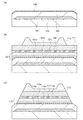
基板101上にゲート電極103を形成する。次に、ゲート電極103を覆ってゲート絶縁層105を形成し、ゲート絶縁層105上に第1の半導体層106を形成する(図1(A)参照)。
A
基板101としては、ガラス基板、セラミック基板の他、本作製工程の処理温度に耐えうる程度の耐熱性を有するプラスチック基板等を用いることができる。また、基板に透光性を要しない場合には、ステンレス合金等の金属の基板の表面に絶縁層を設けたものを用いてもよい。ガラス基板としては、例えば、バリウムホウケイ酸ガラス、アルミノホウケイ酸ガラス若しくはアルミノケイ酸ガラス等の無アルカリガラス基板を用いるとよい。
As the
ゲート電極103は、モリブデン、チタン、クロム、タンタル、タングステン、アルミニウム、銅、ネオジム、スカンジウム等の金属材料またはこれらを主成分とする合金材料を用いて、単層でまたは積層して形成することができる。また、リン等の不純物元素をドーピングした多結晶シリコンに代表される半導体層やAgPdCu合金を用いてもよい。
The
ゲート電極103は、基板101上に、スパッタリング法または真空蒸着法を用いて上記した材料を用いた導電層を形成し、該導電層上にフォトリソグラフィ法またはインクジェット法等によりマスクを形成し、該マスクを用いて導電層をエッチングして形成することができる。フォトリソグラフィ工程においては、レジストを基板全面に塗布してもよいが、レジストマスクを形成する領域に印刷法によりレジストを印刷した後、露光することで、レジストを節約することが可能であり、コスト削減が可能である。
The
また、銀、金または銅等の導電性ナノペーストをインクジェット法により基板上に吐出し、焼成することで形成することもできる。なお、ゲート電極103と、基板101との密着性向上のため、上記の金属材料の窒化物層を、基板101と、ゲート電極103との間に設けてもよい。ここでは、基板101上に導電層を形成し、フォトマスクを用いて形成した第1のレジストマスクによりエッチングする。
Alternatively, a conductive nano paste such as silver, gold, or copper can be formed by discharging onto a substrate by an ink jet method and baking. Note that a nitride layer of the above metal material may be provided between the
なお、ゲート電極103の側面は、テーパー形状とすることが好ましい。ゲート電極103上には、後の工程で半導体層及び配線層を形成するので、段差の箇所における配線切れ防止のためである。ゲート電極103の側面をテーパー形状にするためには、レジストマスクを後退させつつエッチングを行えばよい。
Note that the side surface of the
また、ゲート電極103を形成する工程によりゲート配線(走査線)及び容量配線も同時に形成することができる。なお、走査線とは画素を選択する配線をいい、容量配線とは画素の保持容量の一方の電極に接続された配線をいう。ただし、これに限定されず、ゲート配線及び容量配線の一方または双方と、ゲート電極103とは別に設けてもよい。
Further, a gate wiring (scanning line) and a capacitor wiring can be formed at the same time by the step of forming the
ゲート絶縁層105は、酸化シリコン層、窒化シリコン層、酸化窒化シリコン層または窒化酸化シリコン層を単層でまたは積層して形成することができる。また、ゲート絶縁層105を酸化シリコン層または酸化窒化シリコン層により形成することで、薄膜トランジスタのしきい値電圧の変動を抑制することができる。
The
ゲート絶縁層105は、CVD法またはスパッタリング法等を用いて形成することができる。また、ゲート絶縁層105は、高周波数(1GHz以上)のマイクロ波プラズマCVD装置を用いて形成してもよい。マイクロ波プラズマCVD装置を用いて高い周波数によりゲート絶縁層105を形成すると、ゲート電極と、ドレイン電極及びソース電極との間の耐圧を向上させることができるため、信頼性の高い薄膜トランジスタを得ることができる。また、ゲート絶縁層105として、有機シランガスを用いたCVD法により酸化シリコン層を形成することで、ゲート絶縁層の水素含有量を低減することが可能であり、薄膜トランジスタのしきい値電圧の変動を低減することができる。有機シランガスとしては、珪酸エチル(TEOS:化学式Si(OC2H5)4)、テトラメチルシラン(TMS:化学式Si(CH3)4)、テトラメチルシクロテトラシロキサン(TMCTS)、オクタメチルシクロテトラシロキサン(OMCTS)、ヘキサメチルジシラザン(HMDS)、トリエトキシシラン(SiH(OC2H5)3)、トリスジメチルアミノシラン(SiH(N(CH3)2)3)等のシリコン含有化合物を用いることができる。
The
ゲート絶縁層105上に第1の半導体層106を形成する。第1の半導体層106は、微結晶半導体層を用いて形成し、代表的には微結晶シリコン層、微結晶ゲルマニウム層、微結晶シリコンゲルマニウム層を形成する。第1の半導体層106の厚さは、厚さ3〜10nm、好ましくは3〜5nmと薄くすることで、後に形成される第2の半導体層において、微結晶半導体で形成される複数の錐形状の凸部の長さを制御することができる。
A
第1の半導体層106は、プラズマCVD装置の処理室内において、シリコンまたはゲルマニウムを含む堆積性気体と、水素と、希ガスとを混合し、グロー放電プラズマにより形成する。代表的には、シリコンまたはゲルマニウムを含む堆積性気体と、水素と、ヘリウム、ネオン、アルゴン、キセノン、またはクリプトンとを混合し、グロー放電プラズマにより形成する。シリコンまたはゲルマニウムを含む堆積性気体の流量に対して、水素の流量を10〜2000倍、好ましくは10〜200倍に希釈して、微結晶シリコン、微結晶シリコンゲルマニウム、微結晶ゲルマニウム等を形成する。
The
シリコンまたはゲルマニウムを含む堆積性気体の代表例としては、SiH4、Si2H6、GeH4、Ge2H6等がある。希ガスとしては、ヘリウム、ネオン、アルゴン、キセノン、またはクリプトンの一または複数を用いる。 Typical examples of the deposition gas containing silicon or germanium include SiH 4 , Si 2 H 6 , GeH 4 , and Ge 2 H 6 . As the rare gas, one or more of helium, neon, argon, xenon, or krypton are used.
第1の半導体層106の原料ガスとして、ヘリウム、アルゴン、ネオン、クリプトン、キセノン等の希ガスを用いることで、プラズマが安定し、シリコンまたはゲルマニウムを含む堆積性気体、及び水素の解離が促進され、活性種の量が増加する。このため、活性種同士の反応が促進され、第1の半導体層の成膜速度が高まる。また、成膜速度が高まると、第1の半導体層106が堆積する際に、処理室内の不純物が取り込まれにくくなるため、第1の半導体層106に含まれる不純物量が低減し、第1の半導体層106の結晶性が高まる。このため、薄膜トランジスタのオン電流及び電界効果移動度が高まると共に、薄膜トランジスタの生産性を高めることができる。
By using a rare gas such as helium, argon, neon, krypton, or xenon as a source gas for the
また、第1の半導体層106を形成する際の、グロー放電プラズマの生成は、3MHzから30MHz、代表的には13.56MHz、27.12MHzのHF帯の高周波電力、または30MHzより大きく300MHz程度までのVHF帯の高周波電力、代表的には、60MHzを印加することで行われる。また、1GHz以上のマイクロ波の高周波電力を印加することで行われる。なお、VHF帯やマイクロ波の高周波電力を用いることで、成膜速度を高めることが可能である。更には、HF帯の高周波電力と、VHF帯の高周波電力を重畳させることで、大面積基板においてもプラズマのムラを低減し、均一性を高めることができると共に、成膜速度を高めることができる。
In addition, when the
なお、第1の半導体層106を形成する前に、CVD装置の処理室内を減圧しながら、シリコンまたはゲルマニウムを含む堆積性気体を導入して、処理室内の不純物元素を除去することで、後に形成される薄膜トランジスタのゲート絶縁層105及び第1の半導体層106の界面における不純物元素を低減することが可能であり、薄膜トランジスタの電気特性を向上させることができる。
Note that before the
次に、図1(B)に示すように、第1の半導体層106上に半導体層を堆積して、第2の半導体層107を形成し、第2の半導体層107上に不純物半導体層109を形成し、不純物半導体層109上に導電層111を形成する。その後、導電層111上に第2のレジストマスク113を形成する(図1(B)を参照)。ここでは、第1の半導体層106を種結晶として、部分的に結晶成長させる条件で第2の半導体層107を形成する。なお、プラズマCVD装置の処理室内において、シリコンまたはゲルマニウムを含む堆積性気体と、水素と、窒素を含む気体とを混合し、グロー放電プラズマにより形成する。窒素を含む気体としては、アンモニア、窒素、フッ化窒素、塩化窒素等があるが、これに限定されず窒素を有する気体であればよい。
Next, as illustrated in FIG. 1B, a semiconductor layer is deposited over the
このとき、シリコンまたはゲルマニウムを含む堆積性気体と、水素との流量比は、第1の半導体層106と同様に微結晶半導体層を形成する条件を用い、原料ガスに窒素を含む気体を用いることで、第1の半導体層106の成膜条件よりも、結晶成長を低減する条件とすることができる。なお、第2の半導体層107の成膜条件として、シリコンまたはゲルマニウムを含む堆積性気体と、水素との流量比を、通常の非晶質半導体層を形成する条件とし、かつ窒素を含む気体を用いても、第2の半導体層107において、微結晶半導体及び非晶質半導体を有する層107bを形成することが困難であるため、好ましくない。
At this time, the flow rate ratio between the deposition gas containing silicon or germanium and hydrogen is the same as that of the
ここでは、微結晶半導体層を形成する条件の代表例は、シリコンまたはゲルマニウムを含む堆積性気体の流量に対する水素の流量が10〜2000倍、好ましくは50〜200倍である。なお、通常の非晶質半導体層を形成する条件の代表例は、シリコンまたはゲルマニウムを含む堆積性気体の流量に対する水素の流量は0〜5倍である。 Here, as a typical example of the conditions for forming the microcrystalline semiconductor layer, the flow rate of hydrogen is 10 to 2000 times, preferably 50 to 200 times that of the deposition gas containing silicon or germanium. Note that as a typical example of a condition for forming a normal amorphous semiconductor layer, the flow rate of hydrogen is 0 to 5 times the flow rate of the deposition gas containing silicon or germanium.
また、第2の半導体層107の原料ガスに、ヘリウム、ネオン、アルゴン、キセノン、またはクリプトン等の希ガスを導入し、成膜速度を高めることができる。
In addition, a deposition gas can be increased by introducing a rare gas such as helium, neon, argon, xenon, or krypton into the source gas of the
第2の半導体層107の堆積初期においては、第1の半導体層106を種結晶として、第1の半導体層106上全体的に微結晶半導体層が堆積される(堆積初期)。この後、部分的に、結晶成長が抑制され、錐形状の微結晶半導体領域が成長する(堆積中期)。さらに、錐形状の微結晶半導体領域の結晶成長が抑制され、非晶質半導体層が形成される(堆積後期)。
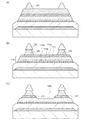
In the initial deposition of the
このことから、図1(B)及び図2(A)に示す第2の半導体層107において、ゲート絶縁層105に接する微結晶半導体層107aが、第1の半導体層106、及び第2の半導体層107の堆積初期に形成される微結晶半導体層に相当する。
Accordingly, in the
また、図1(B)及び図2(A)に示す第2の半導体層107において、微結晶半導体及び非晶質半導体を有する層107bは、第2の半導体層107の堆積中期に形成される錐状の微結晶半導体領域108a、及びその間を充填する非晶質半導体層108bに相当する。
In the
また、図1(B)及び図2(A)に示す第2の半導体層107において、非晶質半導体層107cは、第2の半導体層107の堆積後期に形成される非晶質半導体層に相当する。
In addition, in the
微結晶半導体層107aは、非晶質と結晶構造(単結晶、多結晶を含む)の中間的な構造の半導体で形成される。微結晶半導体は、自由エネルギー的に安定な第3の状態を有する半導体であって、短距離秩序を持ち格子歪みを有する結晶質な半導体であり、結晶粒径が2nm以上200nm以下、好ましくは10nm以上80nm以下、より好ましくは、20nm以上50nm以下の柱状結晶または錐形状結晶が基板表面に対して法線方向に成長している。このため、柱状結晶または錐形状結晶の界面には、結晶粒界が形成される場合もある。
The
微結晶半導体の代表例である微結晶シリコンは、そのラマンスペクトルが単結晶シリコンを示す520cm−1よりも低波数側に、シフトしている。即ち、単結晶シリコンを示す520cm−1とアモルファスシリコンを示す480cm−1の間に微結晶シリコンのラマンスペクトルのピークがある。また、未結合手(ダングリングボンド)を終端するため水素またはハロゲンを少なくとも1原子%またはそれ以上含ませている。さらに、ヘリウム、アルゴン、クリプトン、またはネオンなどの希ガス元素を含ませて格子歪みをさらに助長させることで、安定性が増し良好な微結晶半導体が得られる。このような微結晶半導体に関する記述は、例えば、米国特許4,409,134号で開示されている。 Microcrystalline silicon which is a typical example of a microcrystalline semiconductor has a Raman spectrum shifted to a lower wave number side than 520 cm −1 indicating single crystal silicon. That is, the peak of the Raman spectrum of microcrystalline silicon is between 520 cm −1 indicating single crystal silicon and 480 cm −1 indicating amorphous silicon. In addition, at least 1 atomic% or more of hydrogen or halogen is contained to terminate dangling bonds (dangling bonds). Further, by adding a rare gas element such as helium, argon, krypton, or neon to further promote the lattice distortion, the stability can be improved and a good microcrystalline semiconductor can be obtained. A description of such a microcrystalline semiconductor is disclosed in, for example, US Pat. No. 4,409,134.
また、微結晶半導体層107aに含まれる酸素及び窒素の二次イオン質量分析法によって計測される濃度は、1×10¹⁸atoms/cm3未満とすることで、微結晶半導体層107aの結晶性を高めることができるため好ましい。
The concentration of oxygen and nitrogen contained in the
非晶質半導体層107cは、窒素及び非晶質半導体を有する半導体層、またはNH基及び非晶質半導体を有する半導体層である。ここでの窒素及び非晶質半導体を有する半導体層、またはNH基及び非晶質半導体を有する半導体層の原料ガスの成膜条件として、シリコンまたはゲルマニウムを含む堆積性気体と、水素との流量比を、第1の半導体層106と同様に微結晶半導体層を形成する条件を用い、更に窒素を含む気体を用いることで、通常の窒素を有する非晶質半導体層やNH基を有する非晶質半導体層よりも、CPMや低温PL(フォトルミネッセンス)で測定すると、Urbach端のエネルギーが小さい。また、バンドギャップにおける準位のテール(裾)の傾きが急峻である。即ち、欠陥が少なく、通常の窒素を有する非晶質半導体層やNH基を有する非晶質半導体層より、秩序性が高く、結晶構造を有する。
The
非晶質半導体層107cを、窒素及びアモルファスシリコンを有する半導体層、好ましくはNH基及びアモルファスシリコンを有する半導体層で形成すると、アモルファスシリコンのバンドギャップのバンドテールと比較して、傾斜が急峻となり、バンドギャップが広くなり、トンネル電流が流れにくくなる。この結果、薄膜トランジスタのオフ電流を低減することができる。また、後に形成される薄膜トランジスタのしきい値電圧のシフト量を低減することができる。
When the
図2(A)に示すように、微結晶半導体及び非晶質半導体を有する層107bは、微結晶半導体層107a及び非晶質半導体層107cの間に設けられる。また、微結晶半導体及び非晶質半導体を有する層107bは、微結晶半導体領域108a、及び当該微結晶半導体領域108aの間に充填される非晶質半導体層108bを有する。具体的には、微結晶半導体層107aから凸状に伸びた微結晶半導体領域108aと、非晶質半導体層107cと同様の非晶質半導体層108bとで形成される。
As illustrated in FIG. 2A, the
非晶質半導体層107cを、電気伝導度が低く、抵抗率が高い、窒素を有する非晶質半導体層、またはNH基を有する非晶質半導体層で形成することで、薄膜トランジスタのオフ電流を低減することができる。また、微結晶半導体及び非晶質半導体を有する層107bにおいて、錐形状の微結晶半導体領域108aを有するため、ソース領域またはドレイン領域に電圧が印加されたときの、縦方向(膜厚方向)における抵抗、即ち、第2の半導体層107と、ソース領域またはドレイン領域との間の抵抗を下げることが可能であり、薄膜トランジスタのオン電流を高めることが可能である。
The
また、図2(B)に示すように、微結晶半導体及び非晶質半導体を有する層107bは、微結晶半導体層107a及び不純物半導体層109の間に設けられ、微結晶半導体及び非晶質半導体を有する層107bと不純物半導体層109との間に、非晶質半導体層107cが形成されない構成となる場合がある。このような、図2(B)に示す構造においては、非晶質半導体層108bに対する微結晶半導体領域108aの割合が低いことが好ましい。この結果、薄膜トランジスタのオフ電流を低減することができる。また、微結晶半導体及び非晶質半導体を有する層107bにおいて、ソース領域またはドレイン領域に電圧が印加されたときの、縦方向(膜厚方向)における抵抗、即ち、第2の半導体層107と、ソース領域またはドレイン領域との間の抵抗を下げることが可能であり、薄膜トランジスタのオン電流を高めることが可能である。
As shown in FIG. 2B, the
微結晶半導体領域108aは、ゲート絶縁層105から非晶質半導体層107cへ向けて、先端が狭まる凸状の微結晶半導体である。なお、ゲート絶縁層105から非晶質半導体層107cへ向けて幅が広がる凸の微結晶半導体であってもよい。
The
微結晶半導体及び非晶質半導体を有する層107bにおいては、微結晶半導体領域108aは、ゲート絶縁層105から非晶質半導体層107cへ向けて、先端が狭まる凸状の結晶粒の場合は、微結晶半導体層107a側のほうが、非晶質半導体層107c側と比較して、微結晶半導体領域の割合が高い。これは、微結晶半導体層107aの表面から、微結晶半導体領域108aが膜厚方向に成長するが、原料ガスにおけるシランに対する水素の流量が少ない、または窒素を含む原料ガスの濃度が高いと、微結晶半導体領域108aの結晶粒の成長が抑制され、錐状の結晶粒となるとともに、やがて非晶質半導体層のみが堆積するためである。
In the
また、微結晶半導体及び非晶質半導体を有する層107bは、窒素、代表的にはNH基を有することが好ましい。これは、微結晶半導体領域108aに含まれる結晶粒の界面、微結晶半導体領域108aと非晶質半導体層108bとの界面において、窒素、代表的にはNH基が、シリコン原子のダングリングボンドと結合すると、欠陥が低減し、キャリアが流れやすくなるためである。このため、窒素、好ましくはNH基を1×1020cm−3以上1×1021cm−3以下、好ましくは2×1020cm−3以上1×1021cm−3以下とすることで、シリコン原子のダングリングボンドを窒素、好ましくはNH基で架橋しやすくなり、キャリアが流れやすくなる。この結果、結晶粒界や欠陥におけるキャリアの移動を促進する結合ができ、微結晶半導体及び非晶質半導体を有する層107bの移動度が上昇することがわかる。即ち、薄膜トランジスタの電界効果移動度が上昇する。
The
また、微結晶半導体及び非晶質半導体を有する層107bの酸素濃度を低減することにより、結晶粒と非晶質半導体層との界面や、結晶粒同士の界面における、キャリアの移動を阻害する結合を低減することができる。
In addition, by reducing the oxygen concentration of the
なお、ここでは、微結晶半導体層107aは、概略厚さが等しい領域をいう。また、微結晶半導体層107aと微結晶半導体及び非晶質半導体を有する層107bとの界面は、微結晶半導体領域108aと非晶質半導体層108bとの界面における平坦部において、ゲート絶縁層105に最も近い領域を延長した領域をいう。
Note that here, the
微結晶半導体層107a及び微結晶半導体及び非晶質半導体を有する層107bの厚さの合計、即ち、ゲート絶縁層105の界面から、微結晶半導体及び非晶質半導体を有する層107bの凸部の先端の距離は、3nm以上80nm以下、好ましくは5nm以上30nm以下とすることで、TFTのオフ電流を低減できる。
The total thickness of the
また、第2の半導体層107の原料ガスとして、シリコンまたはゲルマニウムを含む堆積性気体と、水素と共に、窒素を含む気体を用いることで、微結晶半導体及び非晶質半導体を有する層107b、及び非晶質半導体層107cの結晶性と非晶質性を制御することが可能であり、この結果、薄膜トランジスタのしきい値電圧のシフト量を低減することが可能である。
Further, by using a deposition gas containing silicon or germanium as a source gas for the
なお、第2の半導体層107の原料ガスに、ヘリウム、ネオン、アルゴン、キセノン、またはクリプトン等の希ガスを導入する場合は、第2の半導体層107の結晶性が上昇してしまい、薄膜トランジスタのオフ電流が高くなるため、シリコンまたはゲルマニウムを含む堆積性気体と、水素と、窒素を含む気体との混合比を制御することが好ましい。代表的には、非晶質性を高める条件である水素に対するシリコンまたはゲルマニウムを含む堆積性気体を増やす条件とすることで、微結晶半導体及び非晶質半導体を有する層107b、及び非晶質半導体層107cの結晶性と非晶質性を制御することが可能である。
Note that in the case where a rare gas such as helium, neon, argon, xenon, or krypton is introduced into the source gas of the
不純物半導体層109は、プラズマCVD装置の処理室内において、シリコンまたはゲルマニウムを含む堆積性気体と、水素と、フォスフィン(水素希釈またはシラン希釈)とを混合し、グロー放電プラズマにより形成する。シリコンまたはゲルマニウムを含む堆積性気体を水素で希釈して、リンが添加されたアモルファスシリコン、リンが添加された微結晶シリコン、リンが添加されたアモルファスシリコンゲルマニウム、リンが添加された微結晶シリコンゲルマニウム、リンが添加されたアモルファスゲルマニウム、リンが添加された微結晶ゲルマニウム等を形成する。
The
また、不純物半導体層109の原料ガスに、ヘリウム、ネオン、アルゴン、キセノン、またはクリプトン等の希ガスを導入し、成膜速度を高めることができる。
In addition, a rare gas such as helium, neon, argon, xenon, or krypton can be introduced into the source gas of the
なお、第2の半導体層107と、後に形成されるソース電極及びドレイン電極125とがオーミックコンタクトをする場合は、不純物半導体層109を形成しなくともよい。
Note that in the case where the
ゲート絶縁層105の形成から不純物半導体層の形成までについて、図3に示すタイムチャートを参照して以下に説明する。なお、ゲート絶縁層105は、窒化シリコン層上に酸化窒化シリコン層を積層して形成する。
A process from formation of the
まず、ゲート電極103が形成された基板を、実施の形態2に示すCVD装置の処理室241内にて加熱しつつ、窒化シリコン層の堆積に用いる材料ガスを処理室241内に導入する(図3の予備処理201)。ここでは、一例として、SiH4の流量を40sccm、H2の流量を500sccm、N2の流量を550sccm、NH3の流量を140sccmとして材料ガスを導入して安定させ、処理室内の圧力を100Pa、基板の温度を280℃とし、370Wの出力によりプラズマ放電を行うことで、約110nmの窒化シリコン層を形成する。その後、SiH4の供給のみを停止して数秒後にプラズマの放電を停止させる(図3のSiN形成203)。これは、処理室内にSiH4が存在する状態でプラズマの放電を停止させると、シリコンを主成分とする粒状物又は粉状物が形成され、歩留まりを低下させる原因となるためである。
First, a material gas used for deposition of a silicon nitride layer is introduced into the
次に、窒化シリコン層の堆積に用いた材料ガスを排気し、酸化窒化シリコン層の堆積に用いる材料ガスを処理室241内に導入する(図3のガス置換205)。ここでは、一例として、SiH4の流量を30sccm、N2Oの流量を1200sccmとし、材料ガスを導入して安定させ、処理室内の圧力を40Pa、基板の温度を280℃として50Wの出力によりプラズマ放電を行うことで、約110nmの酸化窒化シリコン層を形成する。その後、窒化シリコン層と同様に、SiH4の供給のみを停止し、その数秒後にプラズマの放電を停止させる(図3のSiON形成207)。
Next, the material gas used for depositing the silicon nitride layer is exhausted, and the material gas used for depositing the silicon oxynitride layer is introduced into the treatment chamber 241 (gas replacement 205 in FIG. 3). Here, as an example, the flow rate of SiH 4 is 30 sccm, the flow rate of N 2 O is 1200 sccm, the material gas is introduced and stabilized, the pressure in the processing chamber is 40 Pa, the substrate temperature is 280 ° C., and the plasma is output with 50 W output. By performing discharge, a silicon oxynitride layer having a thickness of about 110 nm is formed. Thereafter, similarly to the silicon nitride layer, only the supply of SiH 4 is stopped, and after a few seconds, plasma discharge is stopped (
上記の工程により、ゲート絶縁層105を形成することができる。ゲート絶縁層105の形成後、基板101を処理室241から搬出する(図3のunload225)。
Through the above steps, the
基板101を処理室241から搬出した後、処理室241に、例えばNF3ガスを導入し、処理室241内をクリーニングする(図3のクリーニング処理227)。その後、処理室241に非晶質シリコン層を形成する処理を行う(図3のプレコート処理229)。この処理により、処理室241の内壁に非晶質シリコン層が形成される。その後、基板101を処理室241内に搬入する(図3のload231)。
After unloading the
次に、第1の半導体層106の堆積に用いる材料ガスを処理室241内に導入する(図3のガス置換209)。次に、ゲート絶縁層105上の全面に第1の半導体層106を形成する。ここでは、一例として、SiH4の流量を10sccm、H2の流量を1500sccm、Arの流量を1500sccmとして材料ガスを導入して安定させ、処理室内の圧力を280Pa、基板の温度を280℃とし、50Wの出力によりプラズマ放電を行うことで、第1の半導体層106として、約5nmの微結晶シリコン層を形成することができる。その後、上記した窒化シリコン層等の形成と同様に、SiH4の供給のみを停止し、その数秒後にプラズマの放電を停止させる(図3の第1の半導体層形成211)。
Next, a material gas used for deposition of the
次に、第1の半導体層106の表面に窒素を供給する。ここでは、第1の半導体層106の表面をアンモニアに曝すことで窒素を供給する(ここでは、フラッシュ処理という。)(図3のフラッシュ処理213)。また、アンモニアには水素を含ませてもよい。または、アンモニアの代わりに窒素ガスを処理室241に導入してもよい。または、アンモニアと窒素ガスを処理室241に導入してもよい。ここでは、一例として、処理室241内の圧力は概ね20Pa〜30Pa、基板の温度は280℃とし、処理時間は60秒間とするとよい。なお、本工程の処理では基板101をアンモニアに曝すのみであるが、プラズマ処理を行ってもよい。その後、これらのガスを排気し、第2の半導体層107の堆積に用いるガスを導入する(図3のガス置換215)。
Next, nitrogen is supplied to the surface of the
次に、第2の半導体層107を形成する。ここで、第2の半導体層107は、窒素を有する非晶質半導体層を用いて形成する。ここでは、一例として、SiH4の流量を30sccm、H2の流量を1425sccm、1000ppmのアンモニア(水素希釈)の流量を25sccmとして材料ガスを導入して安定させ、処理室内の圧力を280Pa、基板の温度を280℃とし、RF電源周波数13.56MHz、RF電源の電力50Wの出力によりプラズマ放電を行うことで、約150nmの第2の半導体層107、ここでは微結晶半導体層107aとして微結晶シリコン層、微結晶半導体及び非晶質半導体を有する層107bとして、微結晶シリコン及びNH基を有するアモルファスシリコンを有する層、非晶質半導体層107cとして窒素を有するアモルファスシリコン層を形成することができる。なお、微結晶半導体及び非晶質半導体を有する層107bの微結晶シリコンに窒素を有してもよい。
Next, the
第2の半導体層107の形成工程において、フラッシュ処理により処理室内に導入されたアンモニアがプラズマ放電により分解され、NH基が生成される。また、第2の半導体層107が堆積される際に、ダングリングボンドを架橋することができる。なお、処理室に窒素を有するガスとして、窒素ガスを導入した場合は、プラズマ放電により、当該窒素ガスと、第2の半導体層107の原料ガスである、水素ガスとが反応し、NH基を生成する。また、当該NH基が第2の半導体層107の異なるダングリングボンドを架橋する。
In the formation process of the
その後、上記した窒化シリコン層等の形成と同様に、SiH4の供給のみを停止し、その数秒後にプラズマの放電を停止させる(図3の第2の半導体層形成217)。その後、これらのガスを排気し、不純物半導体層109の堆積に用いるガスを導入する(図3のガス置換219)。
Thereafter, similarly to the formation of the silicon nitride layer and the like, only the supply of SiH 4 is stopped, and after a few seconds, plasma discharge is stopped (second
本実施の形態における第2の半導体層107を形成する処理室には、窒素を有するガスが供給されている。窒素を有するガスは、プラズマ放電により、NH基が形成される。また、上記したように、NH基は第2の半導体層107に含まれるダングリングボンドを架橋する。このため、窒素を有するガスを供給した処理室において、ダングリングボンドを架橋したNH基を有する非晶質半導体層107cを形成することができる。
A treatment chamber for forming the
このような方法により形成した第2の半導体層107において、二次イオン質量分析法によって計測される窒素濃度は、微結晶半導体層107aと、微結晶半導体及び非晶質半導体を有する層107bとの界面でピーク濃度を有し、微結晶半導体及び非晶質半導体を有する層107b及び非晶質半導体層107cの堆積方向に対して減少する濃度となる。
In the
なお、図3の破線235aに示すように、第2の半導体層形成217において、アンモニアを処理室内に流してもよい。または、アンモニアの代わりに、破線235bに示すように窒素ガスを流してもよい。または、アンモニア及び窒素ガスを流しても良い。この結果、第2の半導体層107の窒素濃度が高まり、第2の半導体層107に含まれるダングリングボンドが架橋され、欠陥準位が低減する。
Note that ammonia may be flowed into the processing chamber in the second
このような方法により形成した第2の半導体層107において、二次イオン質量分析法によって計測される窒素濃度は、微結晶半導体層107a、または微結晶半導体層107aと、微結晶半導体及び非晶質半導体を有する層107bとの界面でピーク濃度を有し、微結晶半導体及び非晶質半導体を有する層107b及び非晶質半導体層107cの堆積方向に対して一定な濃度となる。
In the
また、第2の半導体層形成217において、破線236で示すように、原料ガスとして希ガスを用いてもよい。この結果、第2の半導体層107の成長速度を速めることが可能である。
Further, in the second
次に、第2の半導体層107上の全面に不純物半導体層109を形成する。不純物半導体層109は、後の工程でパターン形成されてソース領域及びドレイン領域127となるものである。まず、不純物半導体層109の堆積に用いる材料ガスを処理室241内に導入する。ここでは、一例として、SiH4の流量を100sccm、PH3をH2により0.5vol%まで希釈した混合ガスの流量を170sccmとして材料ガスを導入して安定させる。処理室241内の圧力を280Pa、基板の温度を280℃とし、60Wの出力によりプラズマ放電を行うことで、約50nmのリンを含むアモルファスシリコン層を形成することができる。その後、上記した窒化シリコン層等の形成と同様に、SiH4の供給のみを停止し、その数秒後にプラズマの放電を停止させる(図3の不純物半導体層形成221)。その後、これらのガスを排気する(図3の排気223)。
Next, the
以上説明したように、不純物半導体層109までを形成することができる。
As described above, up to the
導電層111は、アルミニウム、銅、チタン、ネオジム、スカンジウム、モリブデン、クロム、タンタル若しくはタングステン等により単層で、又は積層して形成することができる。または、ヒロック防止元素が添加されたアルミニウム合金(代表的には、ゲート電極103に用いることができるアルミニウム−ネオジム合金等)により形成してもよい。また、ドナーとなる不純物元素を添加した結晶性シリコンを用いてもよい。ドナーとなる不純物元素が添加された結晶性シリコンと接する側の層を、チタン、タンタル、モリブデン、タングステン又はこれらの元素の窒化物により形成し、その上にアルミニウム又はアルミニウム合金を形成した積層構造としても良い。更には、アルミニウム又はアルミニウム合金の上面及び下面を、チタン、タンタル、モリブデン、タングステン又はこれらの元素の窒化物で挟んだ積層構造としてもよい。例えば、導電層111として、アルミニウム層を窒化チタン層で挟んだ層の積層構造とするとよい。
The
導電層111は、CVD法、スパッタリング法または真空蒸着法を用いて形成する。また、導電層111は、銀、金または銅等の導電性ナノペーストを用いてスクリーン印刷法またはインクジェット法等を用いて吐出し、焼成することで形成しても良い。
The
第2のレジストマスク113は厚さの異なる領域を有する。このようなレジストマスクは、多階調マスクを用いて形成することができる。多階調マスクを用いることで、使用するフォトマスクの枚数が低減され、作製工程数が減少するため好ましい。本実施の形態において、第2の半導体層107のパターンを形成する工程と、ソース領域とドレイン領域を分離する工程において、多階調マスクを用いることができる。
The second resist
多階調マスクとは、多段階の光量で露光を行うことが可能なマスクであり、代表的には、露光領域、半露光領域及び未露光領域の3段階の光量で露光を行う。多階調マスクを用いることで、一度の露光及び現像工程によって、複数(代表的には二種類)の厚さを有するレジストマスクを形成することができる。そのため、多階調マスクを用いることで、フォトマスクの枚数を削減することができる。 A multi-tone mask is a mask that can be exposed with multiple levels of light, and typically, exposure is performed with three levels of light: an exposed area, a half-exposed area, and an unexposed area. By using a multi-tone mask, a resist mask having a plurality of thicknesses (typically two types) can be formed by one exposure and development process. Therefore, the number of photomasks can be reduced by using a multi-tone mask.
図4(A−1)及び図4(B−1)は、代表的な多階調マスクの断面図を示す。図4(A−1)にはグレートーンマスク180を示し、図4(B−1)にはハーフトーンマスク185を示す。
4A-1 and 4B-1 are cross-sectional views of typical multi-tone masks. FIG. 4A-1 shows a
図4(A−1)に示すグレートーンマスク180は、透光性を有する基板181上に遮光層により形成された遮光部182、及び遮光層のパターンが設けられた回折格子部183で構成されている。
A gray-
回折格子部183は、露光に用いる光の解像度限界以下の間隔で設けられたスリット、ドットまたはメッシュ等を有することで、光の透過率を制御する。なお、回折格子部183に設けられるスリット、ドットまたはメッシュは周期的なものであってもよいし、非周期的なものであってもよい。
The
透光性を有する基板181としては、石英等を用いることができる。遮光部182及び回折格子部183を構成する遮光層は、金属を用いて形成すればよく、好ましくはクロムまたは酸化クロム等により設けられる。
As the
グレートーンマスク180に露光するための光を照射した場合、図4(A−2)に示すように、遮光部182に重畳する領域における透光率は0%となり、遮光部182または回折格子部183が設けられていない領域における透光率は100%となる。また、回折格子部183における透光率は、概ね10〜70%の範囲であり、回折格子のスリット、ドットまたはメッシュの間隔等により調整可能である。
When the
図4(B−1)に示すハーフトーンマスク185は、透光性を有する基板186上に半透光層により形成された半透光部187、及び遮光層により形成された遮光部188で構成されている。
A
半透光部187は、MoSiN、MoSi、MoSiO、MoSiON、CrSi等の層を用いて形成することができる。遮光部188は、グレートーンマスクの遮光層と同様の金属を用いて形成すればよく、好ましくはクロムまたは酸化クロム等により設けられる。
The
ハーフトーンマスク185に露光するための光を照射した場合、図4(B−2)に示すように、遮光部188に重畳する領域における透光率は0%となり、遮光部188または半透光部187が設けられていない領域における透光率は100%となる。また、半透光部187における透光率は、概ね10〜70%の範囲であり、形成する材料の種類または形成する膜厚等により、調整可能である。
When light for exposure is applied to the
多階調マスクを用いて露光して現像を行うことで、厚さの異なる領域を有するレジストマスクを形成することができる。 By performing exposure and development using a multi-tone mask, a resist mask having regions with different thicknesses can be formed.
次に、第2のレジストマスク113を用いて、第2の半導体層107、不純物半導体層109、及び導電層111をエッチングする。この工程により、第2の半導体層107、不純物半導体層109及び導電層111を素子毎に分離し、第2の半導体層115、不純物半導体層117、及び導電層119を形成する。なお、第2の半導体層115は、微結晶半導体層115a、微結晶半導体及び非晶質半導体を有する層115b、及び非晶質半導体層115cを有する(図1(C)を参照)。
Next, the
次に、第2のレジストマスク113を後退させて、分離された第3のレジストマスク123を形成する。レジストマスクの後退には、酸素プラズマによるアッシングを用いればよい。ここでは、ゲート電極上で分離するように第2のレジストマスク113をアッシングすることで、第3のレジストマスク123を形成することができる(図5(A)参照)。
Next, the second resist
次に、第3のレジストマスク123を用いて導電層119をエッチングし、ソース電極及びドレイン電極125を形成する(図5(B)を参照)。導電層119のエッチングは、ウエットエッチングを用いることが好ましい。ウエットエッチングにより、導電層が等方的にエッチングされる。その結果、導電層は第3のレジストマスク123よりも内側に後退し、ソース電極及びドレイン電極125が形成される。ソース電極またはドレイン電極125は、ソース電極またはドレイン電極のみならず信号線としても機能する。ただし、これに限定されず、信号線とソース電極及びドレイン電極とは別に設けてもよい。
Next, the
次に、第3のレジストマスク123を用いて、非晶質半導体層115c、及び不純物半導体層117のそれぞれ一部をエッチングする。ここでは、ドライエッチングを用いる。本工程までで、表面に凹部を有する非晶質半導体層129c、ソース領域及びドレイン領域127を形成する(図5(C)参照)。この後、第3のレジストマスク123を除去する。
Next, part of the
なお、ここでは、導電層119をウエットエッチングし、非晶質半導体層115c、及び不純物半導体層117のそれぞれ一部をドライエッチングしたため、導電層119が等方的にエッチングされ、ソース電極及びドレイン電極125の側面と、ソース領域及びドレイン領域127の側面は一致せず、ソース電極及びドレイン電極125の側面の外側に、ソース領域及びドレイン領域127の側面が形成される形状となる。
Note that here, the
また、第3のレジストマスク123を除去した後、不純物半導体層117及び非晶質半導体層115cの一部をエッチングしてもよい。当該エッチングより、ソース電極及びドレイン電極125を用いて不純物半導体層117をエッチングするため、ソース電極及びソース領域のそれぞれ端部が概略一致する。また、ドレイン電極及びドレイン領域のそれぞれ端部が概略一致する。
Alternatively, after removing the third resist
次に、第3のレジストマスク123を除去した後、ドライエッチングを行ってもよい。ドライエッチングの条件は、露出している非晶質半導体層129cにダメージが入らず、且つ非晶質半導体層129cに対するエッチングレートが低い条件を用いる。つまり、露出している非晶質半導体層129c表面にほとんどダメージを与えず、且つ露出している非晶質半導体層129cの厚さがほとんど減少しない条件を用いる。エッチングガスとしては、Cl2に代表される塩素系ガス、CF4、N2等を用いる。また、エッチング方法については特に限定はなく、誘導結合型プラズマ(ICP:Inductively Coupled Plasma)方式、容量結合型プラズマ(CCP:Capacitively Coupled Plasma)方式、電子サイクロトン共鳴プラズマ(ECR:Electron Cyclotron Resonance)方式、反応性イオンエッチング(RIE:Reactive Ion Etching)方式等を用いることができる。
Next, after the third resist
次に、非晶質半導体層129cの表面に水プラズマ、アンモニアプラズマ、窒素プラズマ等を照射してもよい。
Next, the surface of the
水プラズマ処理は、反応空間に水蒸気(H2O蒸気)に代表される、水を主成分とするガスを導入し、プラズマを生成して、行うことができる。 The water plasma treatment can be performed by introducing a gas containing water as a main component typified by water vapor (H 2 O vapor) into the reaction space to generate plasma.
上記したように、ソース領域及びドレイン領域127を形成した後に、非晶質半導体層129cにダメージを与えない条件で更なるドライエッチングを行うことで、露出した非晶質半導体層129c上に存在する残渣などの不純物を除去することができる。また、ドライエッチングに続けて水プラズマ処理を行うことで、レジストマスクの残渣を除去することができる。水プラズマ処理を行うことで、ソース領域とドレイン領域との間の絶縁を確実なものにすることができ、完成する薄膜トランジスタのオフ電流を低減し、電気的特性のばらつきを低減することができる。
As described above, after the source region and the
以上の工程により、少ないマスク数で、オフ電流が低く、オン電流が高く、しきい値電圧が制御された薄膜トランジスタを生産性高く作製することができる。 Through the above process, a thin film transistor with a low number of masks, a low off-state current, a high on-state current, and a controlled threshold voltage can be manufactured with high productivity.
(実施の形態2)
本実施の形態では、ゲート絶縁層105、第1の半導体層106、第2の半導体層107、及び不純物半導体層109の形成に用いることが可能なプラズマCVD装置の一形態について詳細に説明する。これらの層はCVD法等を用いて形成する。
(Embodiment 2)
In this embodiment, one embodiment of a plasma CVD apparatus that can be used for forming the
図6に示すプラズマCVD装置261は、ガス供給手段250及び排気手段251に接続されている。
A
図6に示すプラズマCVD装置261は、処理室241と、ステージ242と、ガス供給部243と、シャワープレート244と、排気口245と、上部電極246と、下部電極247と、交流電源248と、温度制御部249と、を具備する。
A
処理室241は剛性のある素材で形成され、内部を真空排気できるように構成されている。処理室241には、上部電極246と下部電極247が備えられている。なお、図6では、容量結合型(平行平板型)の構成を示しているが、異なる二以上の高周波電力を印加して処理室241の内部にプラズマを生成できるものであれば、誘導結合型など他の構成を適用してもよい。
The
図6に示すプラズマCVD装置により処理を行う際には、所定のガスをガス供給部243から供給する。供給されたガスは、シャワープレート244を通って、処理室241に導入される。上部電極246と下部電極247に接続された交流電源248により、高周波電力が印加されて処理室241内のガスが励起され、プラズマが生成される。また、真空ポンプに接続された排気口245によって、処理室241内のガスが排気されている。また、温度制御部249によって、被処理物を加熱しながらプラズマ処理することができる。
When processing is performed by the plasma CVD apparatus shown in FIG. 6, a predetermined gas is supplied from the
ガス供給手段250は、反応ガスが充填されるシリンダ252、圧力調整弁253、ストップバルブ254、マスフローコントローラ255などで構成されている。処理室241内において、上部電極246と基板101との間には板状に加工され、複数の細孔が設けられたシャワープレートを有する。上部電極246に供給される反応ガスは、中空構造である上部電極246の内部の細孔から処理室241内に供給される。
The gas supply means 250 includes a
処理室241に接続される排気手段251は、真空排気と、反応ガスを流す場合において処理室241内を所定の圧力に保持するように制御する機能が含まれている。排気手段251の構成としては、バタフライバルブ256、コンダクタンスバルブ257、ターボ分子ポンプ258、ドライポンプ259などが含まれる。バタフライバルブ256とコンダクタンスバルブ257を並列に配置する場合には、バタフライバルブ256を閉じてコンダクタンスバルブ257を動作させることで、反応ガスの排気速度を制御して処理室241の圧力を所定の範囲に保つことができる。また、コンダクタンスの大きいバタフライバルブ256を開くことで高真空排気が可能となる。
The
なお、処理室241を10−5Paよりも低い圧力まで超高真空排気する場合には、クライオポンプ260を併用することが好ましい。その他、到達真空度として超高真空まで排気する場合には、処理室241の内壁を鏡面加工し、内壁からのガス放出を低減するためにベーキング用のヒータを設けても良い。
Note that when the
なお、図6に示すように、処理室241の全体を覆って膜が形成(被着)されるようにプレコート処理を行うと、処理室(チャンバー)内壁に付着した不純物元素、または処理室(チャンバー)内壁を構成する不純物元素が素子に混入することを防止することができる。本実施の形態では、プレコート処理はシリコンを主成分とする層を形成すればよく、例えば、非晶質シリコン膜等を形成すればよい。ただし、この膜には酸素が含まれないことが好ましい。
As shown in FIG. 6, when pre-coating treatment is performed so that a film is formed (deposited) so as to cover the
(実施の形態3)
本実施の形態では、実施の形態1に適用可能な第2の半導体層107の形成工程について説明する。
(Embodiment 3)
In this embodiment, a process for forming the
本実施の形態では、第2の半導体層107の形成前に処理室内をクリーニングし、その後チャンバー内壁を窒化シリコン層で覆うことで、第2の半導体層107に窒素を含ませて、酸素濃度を低く抑え、窒素濃度を酸素濃度よりも高くする。ゲート絶縁層105の形成から第1の半導体層106の形成方法は実施の形態1と同様であるため、ここでは、第2の半導体層107から不純物半導体層109の形成までについて、図7を参照して以下に説明する。
In this embodiment mode, the processing chamber is cleaned before the
ゲート絶縁層105上の全面に第1の半導体層106を形成する。まず、第1の半導体層106の堆積に用いる材料ガスを処理室内に導入する。ここでは、一例として、実施の形態1と同様の方法により、第1の半導体層106として約5nmの微結晶シリコン層を形成する。その後、プラズマの放電を停止させる(図7の第1の半導体層形成211)。その後、基板101を処理室241から搬出する(図7のunload225)。
A
基板101を処理室241から搬出した後、処理室241に、例えばNF3ガスを導入し、処理室241内をクリーニングする(図7のクリーニング処理227)。その後、処理室241内に窒化シリコン層を形成する処理を行う(図7のプレコート処理233)。窒化シリコン層としては、実施の形態1のゲート絶縁層で形成した窒化シリコン層と同様の条件を用いる。この処理により、処理室241の内壁に窒化シリコン層が形成される。その後、基板101を処理室241内に搬入する(図7のload231)。
After unloading the
なお、クリーニング処理227は行わなくてもよい。この結果、スループットを向上させることができる。
Note that the
次に、第2の半導体層107の堆積に用いる材料ガスを処理室241内に導入する(図7のガス置換215)。次に、第2の半導体層107を形成する。ここでは、実施の形態1と同様に、厚さ150nmの第2の半導体層107を形成する。具体的には、微結晶半導体層107aとして微結晶シリコン層、微結晶半導体及び非晶質半導体を有する層107bとして、微結晶シリコン及びアモルファスシリコンを有する層、非晶質半導体層107cとして窒素およびアモルファスシリコンを有する半導体層を形成することができる。その後、プラズマの放電を停止させる(図7の第2の半導体層形成217)。
Next, a material gas used for deposition of the
なお、図7の破線237aに示すように、第2の半導体層形成217において、アンモニアを処理室内に流してもよい。または、アンモニアの代わりに、破線237bに示すように窒素ガスを流してもよい。または、アンモニア及び窒素ガスを流しても良い。この結果、第2の半導体層107の窒素濃度が高まり、第2の半導体層107のダングリングボンドが架橋され、欠陥準位が低減する。
Note that ammonia may be allowed to flow into the treatment chamber in the second
このような方法により形成した第2の半導体層107において、二次イオン質量分析法によって計測される窒素濃度は、微結晶半導体層107aの上方、または微結晶半導体層107aと、微結晶半導体及び非晶質半導体を有する層107bとの界面で、ピーク濃度を有し、第2の半導体層107の堆積方向に対して一定な濃度となる。
In the
また、第2の半導体層形成217において、破線238で示すように、原料ガスとして希ガスを用いてもよい。この結果、第2の半導体層107の成長速度を速めることが可能である。
In the second
その後、これらのガスを排気し、不純物半導体層109の堆積に用いるガスを導入する(図7のガス置換219)。また、実施の形態1と同様に、不純物半導体層109を形成する(図7の不純物半導体層形成221)。その後、不純物半導体層109の原料ガスを排気する(図7の排気223)。
After that, these gases are exhausted, and a gas used for depositing the
当該工程において、処理室内にプレコート処理において導入されたアンモニアがプラズマ放電により解離しNH基となる。また、プラズマ放電により、当該窒素ガスと、非晶質半導体層の原料ガスである、水素ガスとが反応しNH基を生成する。また、処理室内の内壁に形成された窒化シリコン層がプラズマに曝されることにより、窒化シリコンの一部が解離しNH基が生成される。 In this process, ammonia introduced in the pre-coating process into the processing chamber is dissociated by plasma discharge and becomes NH groups. Further, by the plasma discharge, the nitrogen gas reacts with hydrogen gas, which is a raw material gas for the amorphous semiconductor layer, to generate NH groups. Further, when the silicon nitride layer formed on the inner wall of the processing chamber is exposed to plasma, part of the silicon nitride is dissociated and NH groups are generated.
本実施の形態において、第2の半導体層107を形成する処理室には、窒素を有するガスが供給され、更にはNH基が生成される。上記したように、NH基はアモルファスシリコン層に含まれるダングリングボンドを架橋する。このため、窒素を有するガスを供給した処理室において、第2の半導体層107を形成することで、ダングリングボンドを架橋したNH基を有する非晶質半導体層を形成することができる。
In this embodiment mode, a treatment chamber in which the
さらに、第2の半導体層を形成する直前に処理室の内壁を窒化シリコン層により覆うことで、酸素濃度を低く抑え、窒素濃度を酸素濃度よりも高くすることが可能であり、NH基を有する非晶質半導体層を形成することができる。 Further, by covering the inner wall of the processing chamber with a silicon nitride layer immediately before forming the second semiconductor layer, the oxygen concentration can be kept low, and the nitrogen concentration can be made higher than the oxygen concentration. An amorphous semiconductor layer can be formed.
また、処理室の内壁を窒化シリコン層で覆うことで、処理室の内壁を構成する元素等が第2の半導体層107に混入することをも防ぐことができる。
In addition, by covering the inner wall of the processing chamber with the silicon nitride layer, it is possible to prevent elements and the like constituting the inner wall of the processing chamber from entering the
なお、上記の説明では、第1の半導体層106を形成した処理室と同様の処理室で第2の半導体層107を形成したため、第1の半導体層106の形成後にクリーニング処理とプレコート処理を行う形態について説明したが、本実施の形態は、実施の形態1と組み合わせて実施してもよい。すなわち、第1の半導体層106を堆積した後、処理室241内に窒化シリコン層を形成し、更にフラッシュ処理213してもよい。
Note that in the above description, since the
以上の工程により、オフ電流が低く、オン電流が高く、しきい値電圧が制御された薄膜トランジスタを生産性高く作製することができる。 Through the above steps, a thin film transistor with a low off-state current, a high on-state current, and a controlled threshold voltage can be manufactured with high productivity.
(実施の形態4)
本実施の形態では、実施の形態1に適用可能な第2の半導体層107の形成工程について説明する。
(Embodiment 4)
In this embodiment, a process for forming the
本実施の形態では、第2の半導体層107の堆積ガスに、窒素を混入させることで、酸素濃度を低く抑え、窒素濃度を酸素濃度よりも高くする。ゲート絶縁層105の形成から第1の半導体層106の形成方法は、実施の形態1と同様であるため、ここでは、第1の半導体層106から不純物半導体層109の形成までについて、図8を参照して以下に説明する。
In this embodiment mode, nitrogen is mixed into the deposition gas of the
ゲート絶縁層105上の全面に第1の半導体層106を形成する。まず、第1の半導体層106の堆積に用いる材料ガスを処理室内に導入する。ここでは、一例として、実施の形態1と同様の方法により、第1の半導体層106として約5nmの微結晶シリコン層を形成する。その後、プラズマの放電を停止させる(図8の第1の半導体層形成211)。その後、これらのガスを排気し、第2の半導体層107の堆積に用いるガスを導入する(図8のガス置換215)。
A
次に、第2の半導体層107を形成する。ここでは、一例として、SiH4の流量を30sccm、H2の流量を1425sccm、1000ppmのNH3(水素希釈)の流量を25sccmとして材料ガスを導入して安定させ、処理室内の圧力を280Pa、基板の温度を280℃とし、RF電源周波数13.56MHz、RF電源の電力50Wの出力によりプラズマ放電を行い、約150nmの第2の半導体層を形成する。具体的には、微結晶半導体層107a、微結晶半導体及び非晶質半導体を有する層107b、及び非晶質半導体層107cを形成する。当該工程において、アンモニアがプラズマ放電により解離しNH基を生成する。さらには、第2の半導体層が堆積される際に、ダングリングボンドを架橋することができる。(図8の第2の半導体層形成217)。
Next, the
なお、処理室に窒素を有するガスとして、アンモニアの代わりに、破線232に示すように窒素ガスを流してもよい。または、アンモニア及び窒素ガスを流しても良い。この結果、第2の半導体層107の窒素濃度が高まり、第2の半導体層107のダングリングボンドが架橋され、欠陥準位が低減する。
As a gas having nitrogen in the treatment chamber, nitrogen gas may be flowed as shown by a broken line 232 instead of ammonia. Alternatively, ammonia and nitrogen gas may be flowed. As a result, the nitrogen concentration in the
このような方法により形成した第2の半導体層107において、二次イオン質量分析法によって計測される窒素濃度は、微結晶半導体層107aの上方、または微結晶半導体層107aと、微結晶半導体及び非晶質半導体を有する層107bとの界面から、不純物半導体層の界面まで一定の濃度を示す。
In the
また、第2の半導体層形成217において、破線234で示すように、原料ガスとして希ガスを用いてもよい。この結果、第2の半導体層107の成長速度を速めることが可能である。
In the second
その後、これらのガスを排気し、不純物半導体層109の堆積に用いるガスを導入する(図8のガス置換219)。また、実施の形態1と同様に、不純物半導体層109を形成する(図8の不純物半導体層形成221)。その後、不純物半導体層109の原料ガスを排気する(図8の排気223)。
After that, these gases are exhausted, and a gas used for depositing the
本実施の形態における第2の半導体層107の堆積ガスには窒素を有するガスが含まれている。窒素を有するガスは、プラズマ放電により、NH基が形成される。上記したように、NH基は第2の半導体層107に含まれるダングリングボンドを架橋する。このため、ダングリングボンドを架橋したNH基を有する非晶質半導体層を形成することができる。その後、不純物半導体層109の原料ガスを排気する(図8の排気223)。
A deposition gas of the
以上の工程により、オフ電流が低く、オン電流が高く、しきい値電圧が制御された薄膜トランジスタを生産性高く作製することができる。 Through the above steps, a thin film transistor with a low off-state current, a high on-state current, and a controlled threshold voltage can be manufactured with high productivity.
(実施の形態5)
実施の形態1において、第2の半導体層107の作製方法について、図9を用いて示す。
(Embodiment 5)
In
本実施の形態では、第2の半導体層107を形成する方法として、実施の形態1において、第1の半導体層形成211処理の後、フラッシュ処理213で窒素を有するガスを処理室内に導入すると共に、第2の半導体層107を形成している途中で(即ち、第2の半導体層形成217において)、実線239aで示すように窒素を有するガスを再度処理室内に導入する(図9参照)。窒素を有するガスとして、ここではアンモニアを用いる。なお、アンモニアの代わりに窒素ガスを用いてもよい。または、アンモニア及び窒素ガスを用いてもよい。この結果、第2の半導体層107の堆積初期及び堆積途中において、窒素濃度が高くなり欠陥準位を低減することができる。
In this embodiment, as a method for forming the
または、第2の半導体層107に、窒素、更にはNH基を添加する方法として、実施の形態3において、第1の半導体層106を形成した後、処理室内に窒化シリコン層を形成すると共に、第2の半導体層107を形成している途中で、窒素を有するガスを再度処理室内に導入してもよい。窒素を有するガスとして、ここではアンモニアを用いる。なお、アンモニアの代わりに窒素ガスを用いてもよい。または、アンモニア及び窒素ガスを用いてもよい。この結果、第2の半導体層107の堆積初期及び堆積途中において、窒素濃度が高くなり欠陥準位を低減することができる。その後、不純物半導体層109の原料ガスを排気する(図9の排気223)。
Alternatively, as a method for adding nitrogen and further an NH group to the
以上の工程により、オフ電流が低く、オン電流が高く、しきい値電圧が制御された薄膜トランジスタを生産性高く作製することができる。 Through the above steps, a thin film transistor with a low off-state current, a high on-state current, and a controlled threshold voltage can be manufactured with high productivity.
(実施の形態6)
実施の形態1とは異なる薄膜トランジスタの作製方法について、図10及び図11を用いて示す。
(Embodiment 6)
A method for manufacturing a thin film transistor, which is different from that in
実施の形態1と同様に、基板101上にゲート電極103を形成する。次に、ゲート電極103を覆ってゲート絶縁層105、第1の半導体層を形成する。次に、実施の形態1と同様に、第1の半導体層から結晶成長させて、第2の半導体層107(微結晶半導体層107a、微結晶半導体及び非晶質半導体を有する層107b、非晶質半導体層107c)を形成する。次に、第2の半導体層107上に不純物半導体層109を形成する。その後、不純物半導体層109上にレジストマスク(図示せず)を形成する(図10(A)を参照)。
Similarly to
次に、レジストマスクを用いて、第2の半導体層107及び不純物半導体層109をエッチングする。この工程により、第2の半導体層107及び不純物半導体層109を素子毎に分離し、第2の半導体層115(微結晶半導体層115a、微結晶半導体及び非晶質半導体を有する層115b、非晶質半導体層115c)、及び不純物半導体層117を形成する(図10(B)を参照)。
Next, the
次に、ゲート絶縁層105、第2の半導体層115、及び不純物半導体層117上に導電層111を形成する(図10(C)参照)。
Next, the
次に、導電層111上にレジストマスク(図示せず。)を形成し、当該レジストマスクを用いて導電層111をエッチングして、ソース電極及びドレイン電極133を形成する(図11(A)参照)。
Next, a resist mask (not shown) is formed over the
次に、ソース電極133ドレイン電極133をマスクとして、不純物半導体層117をエッチングして、ソース領域及びドレイン領域127を形成する。また、非晶質半導体層115cをエッチングして、非晶質半導体層129cを形成する。こののち、レジストマスクを除去する(図11(B)参照)。
Next, the
以上の工程により、薄膜トランジスタを作製することができる。 Through the above process, a thin film transistor can be manufactured.
なお、本実施の形態では、ソース電極及びドレイン電極133を形成した後、レジストマスクを除去せず非晶質半導体層115cの一部をエッチングしたが、当該レジストマスクを除去した後、不純物半導体層117及び非晶質半導体層115cの一部をエッチングしてもよい。当該エッチングより、ソース電極及びドレイン電極133を用いて不純物半導体層117をエッチングするため、ソース電極及びソース領域のそれぞれ端部が概略一致する。また、ドレイン電極及びドレイン領域のそれぞれ端部が概略一致する。
Note that in this embodiment, after the source electrode and the
なお、本実施の形態に示す第2の半導体層107の代わりに、実施の形態3乃至実施の形態5の第2の半導体層107の作製方法を適宜適用することができる。
Note that instead of the
(実施の形態7)
本実施の形態では、チャネル長が10μm以下と短い薄膜トランジスタにおいて、ソース領域及びドレイン領域の抵抗を低減することが可能な形態について、以下に示す。ここでは、実施の形態1を用いて説明するが、適宜他の実施の形態に適用可能である。
(Embodiment 7)
In this embodiment, a mode in which resistance of a source region and a drain region can be reduced in a thin film transistor having a channel length of 10 μm or less is described below. Here, description is made using
不純物半導体層109を、リンが添加された微結晶シリコン、またはボロンが添加された微結晶シリコンで形成する場合は、図1(B)に示す第2の半導体層107において、微結晶半導体及び非晶質半導体を有する層107bまたは非晶質半導体層107cと、不純物半導体層109との間に、微結晶半導体層、代表的には微結晶シリコン層を形成することで、不純物半導体層109の堆積初期に低密度層が形成されず、微結晶半導体層を種結晶として、不純物半導体層109を結晶成長させることが可能であるため、界面の特性を向上させることができる。この結果、不純物半導体層109と、微結晶半導体及び非晶質半導体を有する層107bまたは非晶質半導体層107cとの界面に生じる抵抗を低減することができる。この結果、薄膜トランジスタのソース領域、半導体層、及びドレイン領域を流れる電流量を増加させ、オン電流及び電界効果移動度の増加させることが可能となる。
In the case where the
(実施の形態8)
本実施の形態では、実施の形態1乃至実施の形態7で示す薄膜トランジスタを用いることが可能な、素子基板、及び当該素子基板を有する表示装置について、以下に示す。表示装置としては、液晶表示装置、発光表示装置、電子ペーパー等があるが、上記実施の形態の薄膜トランジスタは他の表示装置の素子基板にも用いることができる。ここでは、上記実施の形態1で示す薄膜トランジスタを有する液晶表示装置、代表的には、VA(Vertical Alignment)型の液晶表示装置について、図12及び図13を用いて説明する。
(Embodiment 8)
In this embodiment, an element substrate in which the thin film transistor described in any of
図12において、液晶表示装置の画素部の断面構造を示す。基板301上に、上記実施の形態で作製される薄膜トランジスタ303及び容量素子305が形成される。また、薄膜トランジスタ303上に形成される絶縁層308上に画素電極309が形成される。薄膜トランジスタ303のソース電極またはドレイン電極307と、画素電極309とは、絶縁層308に設けられる開口部において、接続される。画素電極309上には配向膜311が形成される。
FIG. 12 shows a cross-sectional structure of a pixel portion of a liquid crystal display device. Over the
容量素子305は、薄膜トランジスタ303のゲート電極302と同時に形成される容量配線304と、ゲート絶縁層306と、画素電極309とで構成される。
The
基板301から配向膜311までの積層体を素子基板313という。
A stacked body from the
対向基板321には、薄膜トランジスタ303への光の入射を遮断する遮光層323と、着色層325とが形成される。また、遮光層323及び着色層325上に平坦化層327が形成される。平坦化層327上に対向電極329が形成され、対向電極329上に配向膜331が形成される。
A light-
なお、対向基板321上の、遮光層323、着色層325、及び平坦化層327は、カラーフィルタとして機能する。なお、遮光層323、平坦化層327の何れか一方、または両方は、対向基板321上に形成されていなくともよい。
Note that the light-
また、着色層は、可視光の波長範囲のうち、任意の波長範囲の光を優先的に透過させる機能を有する。通常は、赤色波長範囲の光、青色波長範囲の光、及び緑色波長範囲の光、それぞれを優先的に透過させる着色層を組み合わせて、カラーフィルタに用いることが多い。しかしながら、着色層の組み合わせに関しては、これに限られない。 The colored layer has a function of preferentially transmitting light in an arbitrary wavelength range within the visible light wavelength range. In general, a colored layer that preferentially transmits light in the red wavelength range, light in the blue wavelength range, and light in the green wavelength range is often used in a color filter. However, the combination of the colored layers is not limited to this.
基板301及び対向基板321は、シール材(図示しない)で固定され、基板301、対向基板321、及びシール材の内側に液晶層343が充填される。また、基板301及び対向基板321の間隔を保つために、スペーサ341が設けられている。
The
画素電極309、液晶層343、及び対向電極329が重なり合うことで、液晶素子が形成されている。
The
図13に、図12とは異なる液晶表示装置を示す。ここでは、対向基板321側に着色層が形成されず、薄膜トランジスタ303が形成される基板301側に着色層が形成されることを特徴とする。
FIG. 13 shows a liquid crystal display device different from that in FIG. Here, a coloring layer is not formed on the
図13において、液晶表示装置の画素部の断面構造を示す。基板301上に、上記実施の形態作製される薄膜トランジスタ303及び容量素子305が形成される。
FIG. 13 shows a cross-sectional structure of a pixel portion of a liquid crystal display device. Over the
また、薄膜トランジスタ303上に形成される絶縁層308上に、着色層351が形成される。また、着色層351上には、着色層351に含まれる不純物が液晶層343に混入するのを防ぐために、保護層353が形成される。着色層351及び保護層353上に、画素電極309が形成される。着色層351は、各画素毎に、任意の波長範囲の光(赤色、青色、または緑色)を優先的に透過させる層で形成すればよい。また、着色層351は平坦化層としても機能するため、液晶層343の配向ムラを低減することができる。
A
薄膜トランジスタ303のソース電極またはドレイン電極307と、画素電極309とは、絶縁層308、着色層351、及び保護層353に設けられる開口部において、接続される。画素電極309上には配向膜311が形成される。
The source or
容量素子305は、薄膜トランジスタ303のゲート電極302と同時に形成される容量配線304と、ゲート絶縁層306と、画素電極309とで構成される。
The
基板301から配向膜311までの積層体を素子基板355という。
A stacked body from the
対向基板321には、薄膜トランジスタ303への光の入射を遮断する遮光層323と、遮光層323及び対向基板321を覆う平坦化層327が形成される。平坦化層327上に対向電極329が形成され、対向電極329上に配向膜331が形成される。
A light-
画素電極309、液晶層343、及び対向電極329が重なり合うことで、液晶素子が形成されている。
The
なお、ここでは、液晶表示装置として、VA型の液晶表示装置を示したが、これに限定されない。すなわち、実施の形態1、実施の形態3乃至実施の形態6に示す薄膜トランジスタを用いて形成した素子基板を、FFS型の液晶表示装置、IPS型の液晶表示装置、TN型の液晶表示装置又はその他の液晶表示装置に用いることができる。
Note that although a VA liquid crystal display device is shown here as a liquid crystal display device, the present invention is not limited to this. That is, an element substrate formed using the thin film transistor described in any of
本実施の形態の液晶表示装置は、オン電流及び電解効果移動度が高くオフ電流が低い薄膜トランジスタを画素トランジスタとして用いているため、液晶表示装置の表示画質を高めることができる。また、薄膜トランジスタの大きさを小さくしても、薄膜トランジスタの電気特性が低減されないため、薄膜トランジスタの面積を小さくすることで、液晶表示装置の開口率を向上させることができる。または、画素の面積を小さくすることが可能であり、液晶表示装置の解像度を高めることができる。 Since the liquid crystal display device of this embodiment uses a thin film transistor having a high on-state current and high electrolysis effect mobility and a low off-state current as a pixel transistor, the display image quality of the liquid crystal display device can be improved. In addition, even if the size of the thin film transistor is reduced, the electrical characteristics of the thin film transistor are not reduced; therefore, the aperture ratio of the liquid crystal display device can be improved by reducing the area of the thin film transistor. Alternatively, the pixel area can be reduced, and the resolution of the liquid crystal display device can be increased.
また、図13に示す液晶表示装置は、遮光層323と、着色層351を同一基板上に形成しない。このため、着色層351の形成におけるマスクずれを回避できる。このため、遮光層323の面積を大きくする必要がなくなり、画素における開口率を向上させることができる。
In the liquid crystal display device illustrated in FIG. 13, the light-
(実施の形態9)
実施の形態8で示す素子基板313において、配向膜311を形成せず、発光素子を設けることにより、当該素子基板を発光表示装置や、発光装置に用いることができる。発光表示装置や発光装置は、発光素子として代表的には、エレクトロルミネッセンスを利用する発光素子がある。エレクトロルミネッセンスを利用する発光素子は、発光材料が有機化合物であるか、無機化合物であるかによって大別され、一般的に、前者は有機EL素子、後者は無機EL素子と呼ばれている。
(Embodiment 9)
By providing a light-emitting element without forming the
本実施の形態の発光表示装置及び発光装置は、オン電流及び電解効果移動度が高くオフ電流が低い薄膜トランジスタを画素トランジスタとして用いているため、画質が良好(例えば、高コントラスト)であり、且つ消費電力の低い発光表示装置及び発光装置を作製することができる。 In the light-emitting display device and the light-emitting device of this embodiment, a thin film transistor with high on-state current and high electrolysis effect mobility and low off-state current is used as a pixel transistor, so that the image quality is good (for example, high contrast) and consumption A light-emitting display device and a light-emitting device with low power can be manufactured.
(実施の形態10)
上記実施の形態に係る薄膜トランジスタを有する表示装置は、さまざまな電子機器(遊技機も含む)に適用することができる。電子機器としては、例えば、テレビジョン装置(テレビ、またはテレビジョン受信機ともいう)、コンピュータ用などのモニタ、電子ペーパー、デジタルカメラやデジタルビデオカメラ等のカメラ、デジタルフォトフレーム、携帯電話機(携帯電話、携帯電話装置ともいう)、携帯型ゲーム機、携帯情報端末、音響再生装置、パチンコ機などの大型ゲーム機などが挙げられる。特に、実施の形態8及び実施の形態9で示したように、上記実施の形態に係る薄膜トランジスタを液晶表示装置、発光装置、電気泳動方式表示装置などに適用することにより、電子機器の表示部に用いることができる。以下に具体的に例示する。
(Embodiment 10)
The display device including the thin film transistor according to any of the above embodiments can be applied to various electronic devices (including game machines). Examples of the electronic device include a television device (also referred to as a television or a television receiver), a monitor for a computer, an electronic paper, a camera such as a digital camera or a digital video camera, a digital photo frame, a mobile phone (a mobile phone) Large-sized game machines such as portable game machines, portable information terminals, sound reproduction apparatuses, and pachinko machines. In particular, as described in Embodiments 8 and 9, the thin film transistor according to any of the above embodiments is applied to a liquid crystal display device, a light-emitting device, an electrophoretic display device, or the like, so that the display portion of the electronic device is used. Can be used. Specific examples are given below.
上記実施の形態に係る薄膜トランジスタを有する半導体装置は、電子ペーパーに適用することができる。電子ペーパーは、情報を表示するものであればあらゆる分野の電子機器に用いることが可能である。例えば、電子ペーパーを用いて、電子書籍(電子ブック)、ポスター、電車などの乗り物の車内広告、クレジットカード等の各種カードにおける表示等に適用することができる。電子機器の一例を図14(A)に示す。 The semiconductor device including the thin film transistor according to any of the above embodiments can be applied to electronic paper. Electronic paper can be used for electronic devices in various fields as long as they display information. For example, the electronic paper can be applied to an electronic book (electronic book), a poster, an advertisement in a vehicle such as a train, and a display on various cards such as a credit card. An example of the electronic device is illustrated in FIG.
図14(A)は、電子書籍2700の一例を示している。例えば、電子書籍2700は、筐体2701および筐体2703の2つの筐体で構成されている。筐体2701および筐体2703は、蝶番2711により一体になっており、開閉動作を行うことができる。このような構成により、紙の書籍のような動作を行うことが可能となる。
FIG. 14A illustrates an example of an
筐体2701には表示部2705が組み込まれ、筐体2703には表示部2707が組み込まれている。表示部2705および表示部2707は、続き画面を表示する構成としてもよいし、異なる画面を表示する構成としてもよい。異なる画面を表示する構成とすることで、例えば右側の表示部(図14(A)では表示部2705)に文章を表示し、左側の表示部(図14(A)では表示部2707)に画像を表示することができる。
A
また、図14(A)では、筐体2701に操作部などを備えた例を示している。例えば、筐体2701において、電源2721、操作キー2723、スピーカ2725などを備えている。操作キー2723により、頁を送ることができる。なお、筐体の表示部と同一面にキーボードやポインティングディバイスなどを備える構成としてもよい。また、筐体の裏面や側面に、外部接続用端子(イヤホン端子、USB端子、またはACアダプタおよびUSBケーブルなどの各種ケーブルと接続可能な端子など)、記録媒体挿入部などを備える構成としてもよい。さらに、電子書籍2700は、電子辞書としての機能を持たせた構成としてもよい。
FIG. 14A illustrates an example in which the
また、電子書籍2700は、無線で情報を送受信できる構成としてもよい。無線により、電子書籍サーバから、所望の書籍データなどを購入し、ダウンロードする構成とすることも可能である。
Further, the
図14(B)は、デジタルフォトフレーム9700の一例を示している。例えば、デジタルフォトフレーム9700は、筐体9701に表示部9703が組み込まれている。表示部9703は、各種画像を表示することが可能であり、例えばデジタルカメラなどで撮影した画像データを表示させることで、通常の写真立てと同様に機能させることができる。
FIG. 14B illustrates an example of a
なお、デジタルフォトフレーム9700は、操作部、外部接続用端子(USB端子、USBケーブルなどの各種ケーブルと接続可能な端子など)、記録媒体挿入部などを備える構成とする。これらの構成は、表示部と同一面に組み込まれていてもよいが、側面や裏面に備えるとデザイン性が向上するため好ましい。例えば、デジタルフォトフレームの記録媒体挿入部に、デジタルカメラで撮影した画像データを記憶したメモリを挿入して画像データを取り込み、取り込んだ画像データを表示部9703に表示させることができる。
Note that the
また、デジタルフォトフレーム9700は、無線で情報を送受信出来る構成としてもよい。無線により、所望の画像データを取り込み、表示させる構成とすることもできる。
Further, the
図14(C)は、テレビジョン装置9600の一例を示している。テレビジョン装置9600は、筐体9601に表示部9603が組み込まれている。表示部9603により、映像を表示することが可能である。また、ここでは、スタンド9605により筐体9601を支持した構成を示している。表示部9603は、実施の形態8及び実施の形態9に示した表示装置を適用することができる。
FIG. 14C illustrates an example of a
テレビジョン装置9600の操作は、筐体9601が備える操作スイッチや、別体のリモコン操作機により行うことができる。リモコン操作機が備える操作キーにより、チャンネルや音量の操作を行うことができ、表示部9603に表示される映像を操作することができる。また、リモコン操作機に、当該リモコン操作機から出力する情報を表示する表示部を設ける構成としてもよい。
The
なお、テレビジョン装置9600は、受信機やモデムなどを備えた構成とする。受信機により一般のテレビ放送の受信を行うことができ、さらにモデムを介して有線または無線による通信ネットワークに接続することにより、一方向(送信者から受信者)または双方向(送信者と受信者間、あるいは受信者間同士など)の情報通信を行うことも可能である。
Note that the
図14(D)は、携帯電話機1000の一例を示している。携帯電話機1000は、筐体1001に組み込まれた表示部1002の他、操作ボタン1003、1007、外部接続ポート1004、スピーカ1005、マイク1006などを備えている。表示部1002には、実施の形態8及び実施の形態9に示した表示装置を適用することができる。
FIG. 14D illustrates an example of a
図14(D)に示す携帯電話機1000は、表示部1002がタッチパネルになっており、指などの接触により、表示部1002の表示内容を操作することができる。また、電話の発信、或いはメールの作成は、表示部1002を指などで接触することにより行うことができる。
In the
表示部1002の画面は主として3つのモードがある。第1は、画像の表示を主とする表示モードであり、第2は、文字等の情報の入力を主とする入力モードである。第3は表示モードと入力モードの2つのモードが混合した表示+入力モードである。
There are mainly three screen modes of the
例えば、電話の発信、或いはメールを作成する場合は、表示部1002を文字の入力を主とする文字入力モードとし、画面に表示させた文字の入力操作を行えばよい。この場合、表示部1002の画面の大部分の領域にキーボードまたは番号ボタンを表示させることが好ましい。
For example, when making a call or creating a mail, the
また、携帯電話機1000内部に、ジャイロ、加速度センサ等の傾きを検出するセンサを有する検出装置を設けることで、携帯電話機1000の向き(縦または横)を判断して、表示部1002の表示情報を自動的に切り替えるようにすることができる。
In addition, by providing a detection device having a sensor for detecting the inclination, such as a gyroscope or an acceleration sensor, in the
また、画面モードの切り替えは、表示部1002の接触、又は筐体1001の操作ボタン1007の操作により行われる。また、表示部1002に表示される画像の種類によって切り替えるようにすることもできる。例えば、表示部に表示する画像信号が動画のデータであれば表示モード、テキストデータであれば入力モードに切り替えることができる。
The screen mode is switched by touching the
また、入力モードにおいて、表示部1002の光センサで検出される信号を検知し、表示部1002のタッチ操作による入力が一定期間ない場合には、画面のモードを入力モードから表示モードに切り替えるように制御してもよい。
Further, in the input mode, when a signal detected by the optical sensor of the
表示部1002は、イメージセンサとして機能させることもできる。例えば、表示部1002を掌や指で触れることで、掌紋、指紋等をイメージセンサで撮像することで、本人認証を行うことができる。また、表示部に近赤外光を発光するバックライトまたは近赤外光を発光するセンシング用光源を用いれば、指静脈、掌静脈などを撮像することもできる。
The
本実施の形態は、他の実施の形態に記載した構成と適宜組み合わせて実施することが可能である。 This embodiment can be implemented in appropriate combination with the structures described in the other embodiments.
本実施例では、微結晶シリコン層の原料ガスにおけるアルゴンの有無と成膜速度について、図15(A)を用いて示す。 In this embodiment, the presence / absence of argon in the source gas of the microcrystalline silicon layer and the deposition rate are shown in FIG.
以下に試料の作製方法を示す。 A method for manufacturing the sample is described below.
ガラス基板(旭ガラス社製AN100)上に、厚さ50nmの微結晶シリコン層を形成した。このときの堆積条件は、材料ガスを、流量が1250sccmの水素と、シランと、アルゴンとし、材料ガスをプラズマCVD装置の処理室に導入して安定させ、処理室内の圧力を280Pa、基板の温度を280℃とし、RF電源周波数を13.56MHz、RF電源の電力を50Wとして、プラズマ放電を行った。 A microcrystalline silicon layer having a thickness of 50 nm was formed on a glass substrate (AN100 manufactured by Asahi Glass Co., Ltd.). The deposition conditions at this time are as follows: the material gas is hydrogen having a flow rate of 1250 sccm, silane, and argon; the material gas is introduced into the processing chamber of the plasma CVD apparatus and stabilized; the pressure in the processing chamber is 280 Pa; Was 280 ° C., RF power frequency was 13.56 MHz, RF power was 50 W, and plasma discharge was performed.
このとき、シランの流量をそれぞれ10sccm、20sccm、30sccmとした。また、アルゴンの流量を、それぞれ0sccm、1000sccm、1500sccm、2000sccmとした。 At this time, the flow rates of silane were 10 sccm, 20 sccm, and 30 sccm, respectively. The argon flow rates were 0 sccm, 1000 sccm, 1500 sccm, and 2000 sccm, respectively.
このときのアルゴンの流量と、成膜速度の関係を図15(A)に示す。なお、丸印はシラン流量が10sccmのときの、アルゴンの流量及び成膜速度の関係を示す。また、バツ印は、シランの流量が20sccmのときの、アルゴンの流量及び成膜速度の関係を示す。また、三角印は、シランの流量が30sccmのときの、アルゴンの流量及び成膜速度の関係を示す。また、微結晶シリコン層の厚さの測定は、SCI(Scientific Computing International)社製、光学式薄膜解析システム、FilmTek1000(反射タイプ)を用いて行った。 FIG. 15A shows the relationship between the argon flow rate and the deposition rate at this time. The circles indicate the relationship between the argon flow rate and the deposition rate when the silane flow rate is 10 sccm. The cross marks indicate the relationship between the flow rate of argon and the deposition rate when the flow rate of silane is 20 sccm. The triangle marks indicate the relationship between the flow rate of argon and the deposition rate when the flow rate of silane is 30 sccm. Further, the thickness of the microcrystalline silicon layer was measured by using an optical thin film analysis system, FilmTek 1000 (reflection type) manufactured by SCI (Scientific Computing International).
シランの流量が10〜30sccmで、アルゴンの流量が2000sccmのときの成膜速度は、アルゴンの流量が0sccmの成膜速度の約1.3〜1.6倍である。図15(A)から、アルゴンの流量を増やすほど、微結晶シリコン層の成膜速度が増加したことが分かる。 The deposition rate when the flow rate of silane is 10 to 30 sccm and the flow rate of argon is 2000 sccm is about 1.3 to 1.6 times the deposition rate when the flow rate of argon is 0 sccm. FIG. 15A shows that the deposition rate of the microcrystalline silicon layer increased as the flow rate of argon was increased.
次に、窒素を有する微結晶シリコン層の形成において、希ガスとしてアルゴンの有無による成膜速度について、図15(B)に示す。 Next, FIG. 15B shows the deposition rate with and without argon as a rare gas in forming the microcrystalline silicon layer containing nitrogen.
以下に試料の作製方法を示す。 A method for manufacturing the sample is described below.
ガラス基板(旭ガラス社製AN100)上に、厚さ50nmの窒素を有する微結晶シリコン層を形成した。このときの堆積条件は、材料ガスを、流量が1250sccmの水素と、流量が250sccmの100ppmアンモニア(水素希釈)と、シランと、アルゴンとし、材料ガスを処理室に導入して安定させ、処理室内の圧力を280Pa、基板の温度を280℃とし、RF電源周波数を13.56MHz、RF電源の電力を50Wとしてプラズマ放電を行い、窒素を有する微結晶シリコン層を形成した。 A microcrystalline silicon layer containing nitrogen having a thickness of 50 nm was formed on a glass substrate (AN100 manufactured by Asahi Glass Co., Ltd.). The deposition conditions at this time are as follows: the material gas is hydrogen having a flow rate of 1250 sccm, 100 ppm ammonia (diluted with hydrogen) having a flow rate of 250 sccm, silane, and argon, and the material gas is introduced into the processing chamber to be stabilized. Plasma discharge was performed with a pressure of 280 Pa, a substrate temperature of 280 ° C., an RF power source frequency of 13.56 MHz, and an RF power source power of 50 W to form a microcrystalline silicon layer containing nitrogen.
このとき、シランの流量をそれぞれ10ccm、20sccm、30sccmとした。また、アルゴンの流量を、それぞれ0sccm、1000sccm、1500sccm、2000sccmとした。 At this time, the flow rates of silane were 10 ccm, 20 sccm, and 30 sccm, respectively. The argon flow rates were 0 sccm, 1000 sccm, 1500 sccm, and 2000 sccm, respectively.
このときのアルゴンの流量と、成膜速度の関係を図15(B)に示す。なお、丸印はシラン流量が10sccmのときの、アルゴンの流量及び成膜速度の関係を示す。また、バツ印は、シランの流量が20sccmのときの、アルゴンの流量及び成膜速度の関係を示す。また、三角印は、シランの流量が30sccmのときの、アルゴンの流量及び成膜速度の関係を示す。 FIG. 15B shows the relationship between the argon flow rate and the deposition rate at this time. The circles indicate the relationship between the argon flow rate and the deposition rate when the silane flow rate is 10 sccm. The cross marks indicate the relationship between the flow rate of argon and the deposition rate when the flow rate of silane is 20 sccm. The triangle marks indicate the relationship between the flow rate of argon and the deposition rate when the flow rate of silane is 30 sccm.
シランの流量が10〜30sccmで、アルゴンの流量が2000sccmのときの成膜速度は、アルゴンの流量が0sccmの成膜速度の約1.3〜1.6倍である。図15(B)から、アルゴンの流量を増やすほど、窒素を有する微結晶シリコン層の成膜速度が増加したことが分かる。 The deposition rate when the flow rate of silane is 10 to 30 sccm and the flow rate of argon is 2000 sccm is about 1.3 to 1.6 times the deposition rate when the flow rate of argon is 0 sccm. FIG. 15B shows that as the flow rate of argon is increased, the deposition rate of the microcrystalline silicon layer containing nitrogen is increased.
本実施例では、微結晶シリコン層の原料ガスにおけるアルゴンの有無と微結晶シリコン層の結晶性について、図16及び図17を用いて示す。 In this embodiment, the presence or absence of argon in the source gas of the microcrystalline silicon layer and the crystallinity of the microcrystalline silicon layer are shown with reference to FIGS.
基板上に下地層として、酸化窒化シリコン層を形成した後、酸化窒化シリコン層上に微結晶シリコン層を形成した。 After forming a silicon oxynitride layer over the substrate as a base layer, a microcrystalline silicon layer was formed over the silicon oxynitride layer.
ここでは、基板として、ガラス基板(旭ガラス社製AN100)を用いた。 Here, a glass substrate (AN100 manufactured by Asahi Glass Co., Ltd.) was used as the substrate.
次に、SiH4の流量を30sccm、N2Oの流量を1200sccmとし、材料ガスを導入して安定させ、処理室内の圧力を40Pa、基板の温度を280℃として50Wの出力によりプラズマ放電を行うことで、約100nmの酸化窒化シリコン層を形成した。 Next, the flow rate of SiH 4 is 30 sccm, the flow rate of N 2 O is 1200 sccm, the material gas is introduced and stabilized, the pressure in the processing chamber is 40 Pa, the temperature of the substrate is 280 ° C., and plasma discharge is performed with an output of 50 W. Thus, a silicon oxynitride layer having a thickness of about 100 nm was formed.
次に、SiH4の流量を10sccm、H2の流量を1500sccm、アルゴンの流量を0sccm、500sccm、1000sccm、1500sccm、2000sccmとして、材料ガスを導入して安定させ、処理室内の圧力を280Pa、基板の温度を280℃とし、RF電源周波数を13.56MHz、RF電源の電力を50Wとしてプラズマ放電を行うプラズマCVD法を用いて、厚さ50nmの微結晶シリコン層を形成した。 Next, the flow rate of SiH 4 is set to 10 sccm, the flow rate of H 2 is set to 1500 sccm, the flow rate of argon is set to 0 sccm, 500 sccm, 1000 sccm, 1500 sccm, and 2000 sccm. A microcrystalline silicon layer having a thickness of 50 nm was formed by a plasma CVD method in which plasma discharge was performed at a temperature of 280 ° C., an RF power source frequency of 13.56 MHz, and an RF power source power of 50 W.
次に、微結晶シリコン層の結晶性について、ラマン分光分析を行った。ここでは、HORIBA JOBIN YVON社製のダブルラマン分光装置U−1000を用いてラマン分光分析を行った。 Next, Raman spectroscopic analysis was performed on the crystallinity of the microcrystalline silicon layer. Here, Raman spectroscopic analysis was performed using a double Raman spectroscope U-1000 manufactured by HORIBA JOBIN YVON.
ここでは、代表例として、アルゴンの流量を0sccmとした試料と、アルゴンの流量を1500sccmとした試料のラマン分光分析を行った結果を規格化したラマンスペクトルを図16に示す。実線がアルゴンの流量が1500sccmの試料であり、破線がアルゴンの流量が0sccmの試料のラマンスペクトルである。実線において、ラマンスペクトルのピーク位置が、単結晶シリコンを示す520cm−1側の高波長側に、シフトしていることが分かる。 Here, as a typical example, FIG. 16 shows a Raman spectrum obtained by standardizing the results of Raman spectroscopic analysis of a sample with an argon flow rate of 0 sccm and a sample with an argon flow rate of 1500 sccm. A solid line is a sample with a flow rate of argon of 1500 sccm, and a broken line is a Raman spectrum of a sample with a flow rate of argon of 0 sccm. As can be seen from the solid line, the peak position of the Raman spectrum is shifted to the high wavelength side of 520 cm −1 indicating single crystal silicon.
次に、原料ガスのアルゴンの流量を変えて形成した微結晶シリコン層をラマン分光分析したときの、結晶/非晶質ピーク強度比(Ic/Ia)を、図17(A)に示す。 Next, FIG. 17A shows a crystal / amorphous peak intensity ratio (Ic / Ia) when a microcrystalline silicon layer formed by changing the flow rate of argon as a raw material gas is analyzed by Raman spectroscopy.
アルゴンの流量が増えるにつれ、結晶/非晶質ピーク強度比(Ic/Ia)が大きくなっていることが分かる。 It can be seen that the crystal / amorphous peak intensity ratio (Ic / Ia) increases as the flow rate of argon increases.
次に、原料ガスのアルゴンの流量を変えて形成した微結晶シリコン層をラマン分光分析したときの、ピークシフト値と、半値幅(FWHM)を図17(B)に示す。なお、図17(B)において、左縦軸及び四角印でピークシフト値を示し、右縦軸及び菱形印で半値幅を示す。 Next, FIG. 17B shows a peak shift value and a full width at half maximum (FWHM) when a microcrystalline silicon layer formed by changing the flow rate of argon as a source gas is analyzed by Raman spectroscopy. In FIG. 17B, the left vertical axis and square marks indicate peak shift values, and the right vertical axis and rhombus marks indicate half widths.
アルゴンの流量が増えるにつれ、ピークシフト値が若干上昇し、単結晶シリコンのピークである520cm−1に近づいている。 As the flow rate of argon increases, the peak shift value slightly increases and approaches the single crystal silicon peak of 520 cm −1 .
また、アルゴンの流量が増えるにつれ、半値幅(FWHM)が小さくなっている。 Further, as the flow rate of argon increases, the full width at half maximum (FWHM) decreases.
以上のことから、図16及び図17より、微結晶シリコン層の原料ガスにアルゴンを入れることで、微結晶シリコン層の結晶性が高まっていることが分かる。 From the above, it can be seen from FIGS. 16 and 17 that the crystallinity of the microcrystalline silicon layer is increased by adding argon to the source gas of the microcrystalline silicon layer.
はじめに薄膜トランジスタの作製工程を、図1、図10及び図11を用いて示す。 First, a manufacturing process of a thin film transistor is described with reference to FIGS.
基板101上にゲート電極103を形成した。
A
ここでは、基板101として、ガラス基板(コーニング製EAGLE2000)を用いた。
Here, a glass substrate (Corning EAGLE 2000) was used as the
モリブデンターゲットを流量50sccmのアルゴンイオンでスパッタリングして、厚さ150nmのモリブデン層を基板101上に形成した。次に、モリブデン層上にレジストを塗布した後、第1のフォトマスクを用いて露光した後、現像してレジストマスクを形成した。
A molybdenum target having a thickness of 150 nm was formed on the
次に、当該レジストマスクを用いてモリブデン層をエッチングして、ゲート電極103を形成した。ここでは、ICP(Inductively Coupled Plasma:誘導結合型プラズマ)装置を用い、ICPパワー800W、バイアスパワー100W、圧力1.5Pa、エッチングガスに流量25sccmのフッ化炭素、流量25sccmの塩素、流量10sccmの酸素を用いたエッチング条件を用いた。
Next, the molybdenum layer was etched using the resist mask, so that the
この後、レジストマスクを除去した。 Thereafter, the resist mask was removed.
次に、ゲート電極103及び基板101上に、ゲート絶縁層105、第1の半導体層106を形成した。ここまでの工程を、図1(A)に示す。
Next, the
ここでは、ゲート絶縁層105として厚さ110nmの窒化シリコン層及び厚さ110nmの酸化シリコン層を形成した。
Here, a 110-nm-thick silicon nitride layer and a 110-nm-thick silicon oxide layer were formed as the
窒化シリコン層の堆積条件としては、SiH4の流量を40sccm、H2の流量を500sccm、N2の流量を550sccm、NH3の流量を140sccmとして材料ガスを導入して安定させ、処理室内の圧力を100Pa、基板の温度を280℃とし、RF電源周波数を13.56MHz、RF電源の電力を370Wとしてプラズマ放電を行う、プラズマCVD法を用いた。 The deposition conditions of the silicon nitride layer are as follows: the flow rate of SiH 4 is 40 sccm, the flow rate of H 2 is 500 sccm, the flow rate of N 2 is 550 sccm, the flow rate of NH 3 is 140 sccm, and the material gas is introduced and stabilized. The plasma CVD method was used in which plasma discharge was performed at 100 Pa, the substrate temperature was 280 ° C., the RF power source frequency was 13.56 MHz, and the power of the RF power source was 370 W.
酸化シリコン層の堆積条件としては、オルトケイ酸テトラエチル(Tetraethyl Orthosilicate:TEOS)の流量を15sccm、O2の流量を750sccmとして材料ガスを導入して安定させ、処理室内の圧力を100Pa、上部電極の温度を300℃、下部電極の温度を297℃とし、RF電源周波数を27MHz、RF電源の電力を300Wとしてプラズマ放電を行う、プラズマCVD法を用いた。 The deposition conditions of the silicon oxide layer were as follows: tetraethyl orthosilicate (TEOS) flow rate of 15 sccm, O 2 flow rate of 750 sccm to introduce and stabilize the material gas, the pressure in the processing chamber was 100 Pa, the temperature of the upper electrode The plasma CVD method is used, in which plasma discharge is performed at 300 ° C., the temperature of the lower electrode is 297 ° C., the RF power source frequency is 27 MHz, and the power of the RF power source is 300 W.
ここでは、第1の半導体層106として、厚さ5nmの微結晶シリコン層を形成した。
Here, a microcrystalline silicon layer having a thickness of 5 nm was formed as the
第1の半導体層106の堆積条件を以下に示す。はじめに、処理室内の圧力を100Paとし、処理室に流量300sccmのシランを導入して、処理室内の不純物を除去した。次に、SiH4の流量を10sccm、H2の流量を1500sccm、アルゴンの流量を1500sccmとして材料ガスを導入して安定させ、処理室内の圧力を280Pa、基板の温度を280℃とし、RF電源周波数を13.56MHz、RF電源の電力を50Wとしてプラズマ放電を行うプラズマCVD法を用いた。
The deposition conditions of the
次に、図10(A)に示すように、第2の半導体層107を形成し、第2の半導体層107上に不純物半導体層109を形成した。
Next, as illustrated in FIG. 10A, the
ここでは、厚さ150nmの第2の半導体層107を形成した。また、第2の半導体層107として、微結晶半導体層107aに微結晶シリコン層、微結晶半導体及び非晶質半導体を有する層107bに微結晶シリコン、アモルファスシリコン、及び窒素を有する半導体層、非晶質半導体層107cに窒素及びアモルファスシリコンを有する半導体層を形成した。
Here, the
第2の半導体層107の堆積条件としては、SiH4の流量を30sccm、1000ppmNH3(水素希釈)の流量を25sccm、H2の流量を1475sccmとして材料ガスを導入して安定させ、処理室内の圧力を280Pa、基板の温度を280℃とし、RF電源の電力を50Wとしてプラズマ放電を行った。
As deposition conditions for the
不純物半導体層109として、厚さ50nmのリンが添加されたアモルファスシリコン層を形成した。このときの堆積条件は、堆積温度を280℃、シラン流量100sccm、0.5%フォスフィン(水素希釈)流量を170sccm、圧力170Pa、RF電源周波数を13.56MHz、RF電源の電力を60Wとしてプラズマ放電を行うプラズマCVD法を用いた。
As the
次に、不純物半導体層109上にレジストを塗布した後、第2のフォトマスクを用いて露光し、現像してレジストマスクを形成した。次に、当該レジストマスクを用いて、第2の半導体層107、不純物半導体層109をエッチングして、第2の半導体層115、不純物半導体層117を形成した(図10(B)参照)。ここでは、ICP装置を用い、ソースパワー1000W、バイアスパワー80W、圧力1.51Pa、エッチングガスに流量100sccmの塩素を用いたエッチング条件を用いた。この後レジストマスクを除去した。
Next, after applying a resist over the
次に、図10(C)に示すように、ゲート絶縁層105、第2の半導体層115、不純物半導体層117を覆う導電層111を形成した。ここでは、モリブデンターゲットを流量50sccmのアルゴンイオンでスパッタリングして、厚さ300nmのモリブデン層を形成した。
Next, as illustrated in FIG. 10C, the
次に、導電層119上にレジストを塗布した後、第3のフォトマスクを用いて露光し、現像してレジストマスクを形成した。当該レジストマスクを用いて導電層111をウエットエッチングして、図11(A)に示すように、ソース電極及びドレイン電極133を形成した。ここでは、ウエットエッチングにより、導電層111をエッチングした。なお、本実施例では、ソース電極及びドレイン電極133の平面形状は、並行型である。
Next, a resist was applied over the
次に、レジストマスクを用いて不純物半導体層117エッチングして、ソース領域及びドレイン領域127形成した。なお、当該工程において、第2の半導体層115の一部もエッチングされ、凹部を有する非晶質半導体層129cが形成された(図11(B)参照)。ここでは、ICPパワー150W、バイアスパワー40W、圧力1.2Pa、エッチングガスに流量100sccmの塩素を用いたエッチング条件を用い、90nmエッチングした。このときの、微結晶半導体層115a、微結晶半導体及び非晶質半導体を有する層115b、及び非晶質半導体層129cのエッチングされた領域の合計の厚さを110nmとした。
Next, the
次に、レジストマスクを除去した後、非晶質半導体層129c、ソース領域及びドレイン領域127表面にフッ化炭素プラズマを照射し、非晶質半導体層129cの表面に残留する不純物を除去した。ここでは、ソースパワー1000W、バイアスパワー0W、圧力0.67Pa、エッチングガスに流量100sccmのフッ化炭素を用いたエッチング条件を用いた。
Next, after removing the resist mask, the surface of the
次に、絶縁層として、窒化シリコン層を形成した。このときの堆積条件は、SiH4の流量を20sccm、NH3の流量を220sccm、窒素の流量を450sccm、水素の流量を450sccmとして材料ガスを導入し、処理室内の圧力を160Pa、基板の温度を250℃とし、200Wの出力によりプラズマ放電を行って、厚さ300nmの窒化シリコン層を形成した。 Next, a silicon nitride layer was formed as an insulating layer. The deposition conditions at this time are as follows: the flow rate of SiH 4 is 20 sccm, the flow rate of NH 3 is 220 sccm, the flow rate of nitrogen is 450 sccm, the flow rate of hydrogen is 450 sccm, the material gas is introduced, the pressure in the processing chamber is 160 Pa, and the temperature of the substrate is set. Plasma discharge was performed at 250 ° C. and an output of 200 W to form a silicon nitride layer having a thickness of 300 nm.
次に、絶縁層上にレジストを塗布した後、第4のフォトマスクを用いて露光し、現像してレジストマスクを形成した。当該レジストマスクを用いて絶縁層の一部をドライエッチングして、ソース電極及びドレイン電極133を露出した。また、絶縁層及びゲート絶縁層105の一部をドライエッチングして、ゲート電極103を露出した。この後、レジストマスクを除去した。
Next, a resist was applied over the insulating layer, and then exposed using a fourth photomask and developed to form a resist mask. A part of the insulating layer was dry etched using the resist mask to expose the source and drain
以上の工程により、薄膜トランジスタを作製した。 Through the above steps, a thin film transistor was manufactured.
こののち、薄膜トランジスタの電気特性を測定した結果を図18に示す。ドレイン電圧が1V及び10Vの電流電圧特性及び電界効果移動度を実線で示した。なお、本実施例の薄膜トランジスタのチャネル長を3.5μm、チャネル幅を20μmとして形成した。 After that, the result of measuring the electrical characteristics of the thin film transistor is shown in FIG. The current-voltage characteristics and field-effect mobility with a drain voltage of 1 V and 10 V are indicated by solid lines. Note that the thin film transistor of this example was formed with a channel length of 3.5 μm and a channel width of 20 μm.
このときの、16個の薄膜トランジスタの電気特性を測定した平均値を以下に示す。しきい値電圧(Vth)は2.83V、Vdが1Vのときの電界効果移動度は0.65cm2/Vs、Vdが10Vのときの電界効果移動度は0.59cm2/Vs、S値は0.46V/decであった。また、Vdが10Vで、Vgが15Vのときのオン電流(Ion)は5.13μA、最小オフ電流(Ioff_min)は0.31pA、Vgが−14Vのときのオフ電流(Ioff)は9.6pAであった。このことから、しきい値電圧のシフトが少なく、オン電流が高く、オフ電流が低い、良好な電気特性を有する薄膜トランジスタを作製することができた。
The average value obtained by measuring the electrical characteristics of the 16 thin film transistors is shown below. Threshold voltage (Vth) is 2.83V, field-effect mobility of when the field effect mobility is 0.65 cm 2 / Vs, the
本実施例では、微結晶シリコン層の原料ガスにおけるアルゴンの有無と微結晶シリコン層含まれる不純物について、図19及び図20を用いて示す。 In this embodiment, the presence or absence of argon in the source gas of the microcrystalline silicon layer and the impurities contained in the microcrystalline silicon layer are shown with reference to FIGS.
はじめに試料の作製方法について示す。 First, a method for manufacturing a sample is described.
基板上に下地層として、窒化シリコン層を形成し、窒化シリコン層上に酸化窒化シリコン層を形成した後、酸化窒化シリコン層上に微結晶シリコン層を形成した。また、微結晶シリコン層上に保護層としてアモルファスシリコン層を形成した。 A silicon nitride layer was formed as a base layer over the substrate, a silicon oxynitride layer was formed over the silicon nitride layer, and then a microcrystalline silicon layer was formed over the silicon oxynitride layer. In addition, an amorphous silicon layer was formed as a protective layer over the microcrystalline silicon layer.
ここでは、基板として、ガラス基板(旭ガラス社製AN100)を用いた。 Here, a glass substrate (AN100 manufactured by Asahi Glass Co., Ltd.) was used as the substrate.
窒化シリコン層の堆積条件としては、SiH4の流量を40sccm、H2の流量を500sccm、N2の流量を550sccm、NH3の流量を140sccmとして材料ガスを導入して安定させ、処理室内の圧力を100Pa、基板の温度を280℃とし、RF電源周波数を13.56MHz、RF電源の電力を370Wとしてプラズマ放電を行う、プラズマCVD法を用いた。 The deposition conditions of the silicon nitride layer are as follows: the flow rate of SiH 4 is 40 sccm, the flow rate of H 2 is 500 sccm, the flow rate of N 2 is 550 sccm, the flow rate of NH 3 is 140 sccm, and the material gas is introduced and stabilized. The plasma CVD method was used in which plasma discharge was performed at 100 Pa, the substrate temperature was 280 ° C., the RF power source frequency was 13.56 MHz, and the power of the RF power source was 370 W.
次に、SiH4の流量を30sccm、N2Oの流量を1200sccmとし、材料ガスを導入して安定させ、処理室内の圧力を40Pa、基板の温度を280℃として50Wの出力によりプラズマ放電を行うことで、約100nmの酸化窒化シリコン層(図19及び図20においてはSiONと示す。)を形成した。 Next, the flow rate of SiH 4 is 30 sccm, the flow rate of N 2 O is 1200 sccm, the material gas is introduced and stabilized, the pressure in the processing chamber is 40 Pa, the temperature of the substrate is 280 ° C., and plasma discharge is performed with an output of 50 W. Thus, a silicon oxynitride layer (shown as SiON in FIGS. 19 and 20) of about 100 nm was formed.
次に、プラズマCVD装置の処理室から基板を搬出した後、NF3で処理室内をクリーニングした後、処理室内に保護膜として酸化シリコン層を形成した。 Next, after unloading the substrate from the processing chamber of the plasma CVD apparatus, the processing chamber was cleaned with NF 3 , and a silicon oxide layer was formed as a protective film in the processing chamber.
次に、SiH4の流量を10sccm、H2の流量を1500sccm、アルゴンの流量を0sccmまたは1500sccmとして、材料ガスを導入して安定させ、処理室内の圧力を280Pa、基板の温度を280℃とし、RF電源周波数を13.56MHz、RF電源の電力を50Wとしてプラズマ放電を行うプラズマCVD法を用いて、厚さ100nmの微結晶シリコン層(図19及び図20においてはμc−Siと示す。)を形成した。 Next, the flow rate of SiH 4 is 10 sccm, the flow rate of H 2 is 1500 sccm, the flow rate of argon is 0 sccm or 1500 sccm, the material gas is introduced and stabilized, the pressure in the processing chamber is 280 Pa, the temperature of the substrate is 280 ° C., Using a plasma CVD method in which plasma discharge is performed with an RF power source frequency of 13.56 MHz and an RF power source power of 50 W, a microcrystalline silicon layer (shown as μc-Si in FIGS. 19 and 20) is used. Formed.
次に、保護層として、微結晶シリコン層上に厚さ100nmのアモルファスシリコン層(図19及び図20においてはa−Siと示す。)を形成した。 Next, as the protective layer, an amorphous silicon layer (shown as a-Si in FIGS. 19 and 20) with a thickness of 100 nm was formed over the microcrystalline silicon layer.
次に、各試料をSIMS測定した結果を図19及び図20に示す。図19は窒素濃度を示し、図20はアルゴン濃度を示す。図19及び図20において、微結晶シリコン層の原料ガスにおけるアルゴンの流量が0sccmの試料の濃度プロファイルを破線で示し、アルゴンの流量が1500sccmの試料の濃度プロファイルを実線で示す。 Next, the results of SIMS measurement of each sample are shown in FIGS. FIG. 19 shows the nitrogen concentration, and FIG. 20 shows the argon concentration. 19 and 20, the concentration profile of a sample with an argon flow rate of 0 sccm in the source gas of the microcrystalline silicon layer is indicated by a broken line, and the concentration profile of a sample with an argon flow rate of 1500 sccm is indicated by a solid line.
図19より、原料ガスにおけるアルゴンの流量が1500sccmの微結晶シリコン層(μc−Si)は窒素濃度が低減していることがわかる。このことから、原料ガスとしてアルゴンを用いることで、微結晶シリコン層の不純物濃度を低減できることがわかる。一方、図20より原料ガスにアルゴンを用いても微結晶シリコン層に含まれるアルゴンの量は検出下限以下である。このため、原料ガスにアルゴンを用いても微結晶シリコン層にアルゴンは取り込まれにくいことがわかる。 FIG. 19 shows that the nitrogen concentration of the microcrystalline silicon layer (μc-Si) having a flow rate of argon in the source gas of 1500 sccm is reduced. This shows that the impurity concentration of the microcrystalline silicon layer can be reduced by using argon as a source gas. On the other hand, from FIG. 20, even if argon is used as the source gas, the amount of argon contained in the microcrystalline silicon layer is below the detection lower limit. Therefore, it can be seen that even if argon is used as the source gas, argon is hardly taken into the microcrystalline silicon layer.
Claims (3)
前記ゲート電極上のゲート絶縁層と、
前記ゲート絶縁層上の半導体層と、
前記半導体層上の不純物元素を含む半導体層と、
前記不純物元素を含む半導体層上のソース電極とドレイン電極とを有する薄膜トランジスタの作製方法であって、
前記半導体層は、前記ゲート絶縁層側から、第1の層と、前記第1の層上の第2の層と、前記第2の層上の第3の層とを有し、
前記第1の層は、微結晶半導体層であり、
前記第2の層は、微結晶半導体領域と、非晶質半導体領域とを有し、
前記第3の層は、非晶質半導体層であり、
前記第1の層は、前記ゲート絶縁層側の第1の領域と、前記第1の部分上の第2の領域とを有し、
シリコンまたはゲルマニウムを含む堆積性気体と、水素と、希ガスとを混合し、シリコンまたはゲルマニウムを含む堆積性気体の流量に対して、水素の流量を10〜2000倍にし、高周波電力を印加することで、前記第1の領域を形成し、
前記第1の領域を形成後、シリコンまたはゲルマニウムを含む堆積性気体と、水素と、窒素を含む気体を混合し、シリコンまたはゲルマニウムを含む堆積性気体の流量に対して、水素の流量を10〜2000倍にし、高周波電力を印加することで、前記第2の領域と前記第2の層と前記第3の層とを形成することを特徴とする薄膜トランジスタの作製方法。 A gate electrode on the substrate,
A gate insulating layer on the gate electrode,
A semiconductor layer on the gate insulating layer,
A semiconductor layer including an impurity element on the semiconductor layer,
A method for manufacturing a thin film transistor having a source electrode and a drain electrode on a semiconductor layer containing the impurity element ,
The semiconductor layer includes, from the gate insulating layer side, a first layer, a second layer on the first layer, and a third layer on the second layer,
The first layer is a microcrystalline semiconductor layer;
The second layer has a microcrystalline semiconductor region and an amorphous semiconductor region,
The third layer is an amorphous semiconductor layer;
The first layer has a first region on the gate insulating layer side and a second region on the first portion;
A deposition gas containing silicon or germanium, hydrogen, and a rare gas are mixed, the flow rate of hydrogen is 10 to 2000 times the flow rate of the deposition gas containing silicon or germanium, and high frequency power is applied . And forming the first region ,
After forming the first region, a deposition gas containing silicon or germanium, hydrogen, and a gas containing nitrogen are mixed, and the flow rate of hydrogen is set to 10 to 10 with respect to the flow rate of the deposition gas containing silicon or germanium. A method for manufacturing a thin film transistor, characterized in that the second region, the second layer, and the third layer are formed by applying high-frequency power at a magnification of 2000 times .
前記第2の領域は、前記第1の領域を種結晶として結晶成長することで形成されることを特徴とする薄膜トランジスタの作製方法。The method of manufacturing a thin film transistor, wherein the second region is formed by crystal growth using the first region as a seed crystal.
前記第2の層の前記微結晶半導体領域は、前記第1の層から前記第3の層に向かって、先端が狭まる凸状の領域であり、The microcrystalline semiconductor region of the second layer is a convex region whose tip narrows from the first layer toward the third layer;
前記第2の層の前記微結晶半導体領域以外は、前記非晶質半導体領域であることを特徴とする薄膜トランジスタの作製方法。A method for manufacturing a thin film transistor, wherein the second semiconductor layer is an amorphous semiconductor region other than the microcrystalline semiconductor region.
Priority Applications (1)
| Application Number | Priority Date | Filing Date | Title |
|---|---|---|---|
| JP2009257696A JP5498762B2 (en) | 2008-11-17 | 2009-11-11 | Method for manufacturing thin film transistor |
Applications Claiming Priority (3)
| Application Number | Priority Date | Filing Date | Title |
|---|---|---|---|
| JP2008293954 | 2008-11-17 | ||
| JP2008293954 | 2008-11-17 | ||
| JP2009257696A JP5498762B2 (en) | 2008-11-17 | 2009-11-11 | Method for manufacturing thin film transistor |
Publications (3)
| Publication Number | Publication Date |
|---|---|
| JP2010141306A JP2010141306A (en) | 2010-06-24 |
| JP2010141306A5 JP2010141306A5 (en) | 2012-12-20 |
| JP5498762B2 true JP5498762B2 (en) | 2014-05-21 |
Family
ID=42172354
Family Applications (1)
| Application Number | Title | Priority Date | Filing Date |
|---|---|---|---|
| JP2009257696A Expired - Fee Related JP5498762B2 (en) | 2008-11-17 | 2009-11-11 | Method for manufacturing thin film transistor |
Country Status (2)
| Country | Link |
|---|---|
| US (1) | US8569120B2 (en) |
| JP (1) | JP5498762B2 (en) |
Families Citing this family (8)
| Publication number | Priority date | Publication date | Assignee | Title |
|---|---|---|---|---|
| JP5525224B2 (en) | 2008-09-30 | 2014-06-18 | 株式会社半導体エネルギー研究所 | Display device |
| US8383434B2 (en) * | 2010-02-22 | 2013-02-26 | Semiconductor Energy Laboratory Co., Ltd. | Thin film transistor and manufacturing method thereof |
| TWI606490B (en) | 2010-07-02 | 2017-11-21 | 半導體能源研究所股份有限公司 | Manufacturing method of semiconductor film, manufacturing method of semiconductor device, and manufacturing method of photoelectric conversion device |
| JP5948025B2 (en) | 2010-08-06 | 2016-07-06 | 株式会社半導体エネルギー研究所 | Liquid crystal display |
| US8895116B2 (en) | 2010-11-04 | 2014-11-25 | Semiconductor Energy Laboratory Co., Ltd. | Manufacturing method of crystalline semiconductor film and manufacturing method of semiconductor device |
| US9048327B2 (en) * | 2011-01-25 | 2015-06-02 | Semiconductor Energy Laboratory Co., Ltd. | Microcrystalline semiconductor film, method for manufacturing the same, and method for manufacturing semiconductor device |
| JP6006948B2 (en) * | 2011-03-17 | 2016-10-12 | 株式会社半導体エネルギー研究所 | Microcrystalline semiconductor film and method for manufacturing semiconductor device |
| CN110797357A (en) * | 2018-08-02 | 2020-02-14 | 夏普株式会社 | Image pickup panel and method for manufacturing same |
Family Cites Families (54)
| Publication number | Priority date | Publication date | Assignee | Title |
|---|---|---|---|---|
| JPS56122123A (en) | 1980-03-03 | 1981-09-25 | Shunpei Yamazaki | Semiamorphous semiconductor |
| US5091334A (en) | 1980-03-03 | 1992-02-25 | Semiconductor Energy Laboratory Co., Ltd. | Semiconductor device |
| JPS5771126A (en) | 1980-10-21 | 1982-05-01 | Semiconductor Energy Lab Co Ltd | Semiamorhous semiconductor |
| JPS5892217A (en) | 1981-11-28 | 1983-06-01 | Semiconductor Energy Lab Co Ltd | Manufacture of semiconductor device |
| JPS5972781A (en) | 1982-10-20 | 1984-04-24 | Semiconductor Energy Lab Co Ltd | Photoelectric conversion semiconductor device |
| JPS6027122A (en) * | 1983-07-22 | 1985-02-12 | Semiconductor Energy Lab Co Ltd | Method of photo plasma gas phase reaction |
| JPS60160170A (en) | 1984-01-31 | 1985-08-21 | Seiko Instr & Electronics Ltd | Thin film transistor |
| JPS62141776A (en) * | 1985-12-17 | 1987-06-25 | Hitachi Ltd | Thin film transistor |
| US5221631A (en) | 1989-02-17 | 1993-06-22 | International Business Machines Corporation | Method of fabricating a thin film transistor having a silicon carbide buffer layer |
| JP2839529B2 (en) | 1989-02-17 | 1998-12-16 | 株式会社東芝 | Thin film transistor |
| JPH03278466A (en) | 1990-03-27 | 1991-12-10 | Toshiba Corp | Thin film transistor and manufacture thereof |
| KR950013784B1 (en) | 1990-11-20 | 1995-11-16 | 가부시키가이샤 한도오따이 에네루기 겐큐쇼 | Field effect trasistor and its making method and tft |
| US7115902B1 (en) | 1990-11-20 | 2006-10-03 | Semiconductor Energy Laboratory Co., Ltd. | Electro-optical device and method for manufacturing the same |
| US5514879A (en) | 1990-11-20 | 1996-05-07 | Semiconductor Energy Laboratory Co., Ltd. | Gate insulated field effect transistors and method of manufacturing the same |
| US5849601A (en) | 1990-12-25 | 1998-12-15 | Semiconductor Energy Laboratory Co., Ltd. | Electro-optical device and method for manufacturing the same |
| US7098479B1 (en) | 1990-12-25 | 2006-08-29 | Semiconductor Energy Laboratory Co., Ltd. | Electro-optical device and method for manufacturing the same |
| JPH04266019A (en) | 1991-02-20 | 1992-09-22 | Canon Inc | Film formation |
| JP3255942B2 (en) | 1991-06-19 | 2002-02-12 | 株式会社半導体エネルギー研究所 | Method for manufacturing inverted staggered thin film transistor |
| EP0535979A3 (en) | 1991-10-02 | 1993-07-21 | Sharp Kabushiki Kaisha | A thin film transistor and a method for producing the same |
| JPH05129608A (en) | 1991-10-31 | 1993-05-25 | Sharp Corp | Semiconductor device |
| US6835523B1 (en) | 1993-05-09 | 2004-12-28 | Semiconductor Energy Laboratory Co., Ltd. | Apparatus for fabricating coating and method of fabricating the coating |
| JPH06326312A (en) | 1993-05-14 | 1994-11-25 | Toshiba Corp | Active matrix type display device |
| US5932302A (en) | 1993-07-20 | 1999-08-03 | Semiconductor Energy Laboratory Co., Ltd. | Method for fabricating with ultrasonic vibration a carbon coating |
| JPH07131030A (en) | 1993-11-05 | 1995-05-19 | Sony Corp | Thin film semiconductor device for display and fabrication thereof |
| TW303526B (en) | 1994-12-27 | 1997-04-21 | Matsushita Electric Ind Co Ltd | |
| US5677236A (en) | 1995-02-24 | 1997-10-14 | Mitsui Toatsu Chemicals, Inc. | Process for forming a thin microcrystalline silicon semiconductor film |
| US5920772A (en) | 1997-06-27 | 1999-07-06 | Industrial Technology Research Institute | Method of fabricating a hybrid polysilicon/amorphous silicon TFT |
| JP2000277439A (en) | 1999-03-25 | 2000-10-06 | Kanegafuchi Chem Ind Co Ltd | Plasma cvd method for crystalline silicon thin-film and manufacture of silicon thin-film photoelectric conversion device |
| JP2001007024A (en) | 1999-06-18 | 2001-01-12 | Sanyo Electric Co Ltd | Method of forming of polycrystalline silicon film |
| JP2001053283A (en) | 1999-08-12 | 2001-02-23 | Semiconductor Energy Lab Co Ltd | Semiconductor device and its manufacture |
| KR100436181B1 (en) | 2002-04-16 | 2004-06-12 | 엘지.필립스 엘시디 주식회사 | method for fabricating of an array substrate for a liquid crystal display device |
| JP2004014958A (en) | 2002-06-11 | 2004-01-15 | Fuji Electric Holdings Co Ltd | Thin film polycrystalline solar cell and manufacturing method therefor |
| CN100552893C (en) | 2003-03-26 | 2009-10-21 | 株式会社半导体能源研究所 | Semiconductor device and manufacture method thereof |
| JP4748954B2 (en) | 2003-07-14 | 2011-08-17 | 株式会社半導体エネルギー研究所 | Liquid crystal display |
| US8319219B2 (en) | 2003-07-14 | 2012-11-27 | Semiconductor Energy Laboratory Co., Ltd. | Light-emitting device |
| TWI336921B (en) | 2003-07-18 | 2011-02-01 | Semiconductor Energy Lab | Method for manufacturing semiconductor device |
| US7211454B2 (en) | 2003-07-25 | 2007-05-01 | Semiconductor Energy Laboratory Co., Ltd. | Manufacturing method of a light emitting device including moving the source of the vapor deposition parallel to the substrate |
| JP2005050905A (en) | 2003-07-30 | 2005-02-24 | Sharp Corp | Method for manufacturing silicon thin film solar cell |
| KR101188356B1 (en) | 2003-12-02 | 2012-10-08 | 가부시키가이샤 한도오따이 에네루기 켄큐쇼 | Laser irradiation apparatus, laser irradiation method, and method for manufacturing semiconductor device |
| JP5159021B2 (en) | 2003-12-02 | 2013-03-06 | 株式会社半導体エネルギー研究所 | Method for manufacturing semiconductor device |
| JP2005167051A (en) | 2003-12-04 | 2005-06-23 | Sony Corp | Thin film transistor and manufacturing method thereof |
| US7753751B2 (en) * | 2004-09-29 | 2010-07-13 | Semiconductor Energy Laboratory Co., Ltd. | Method of fabricating the display device |
| FR2893951B1 (en) * | 2005-11-30 | 2008-02-29 | Centre Nat Rech Scient | PROCESS FOR THE PRODUCTION IN ACTIVE AND STABLE TRANSPOSASES OF PROCINOTOES OF MARINER MOBILE GENETIC ELEMENTS |
| JP2008124392A (en) * | 2006-11-15 | 2008-05-29 | Sharp Corp | Semiconductor device, manufacturing method thereof, and display device |
| JP5331389B2 (en) | 2007-06-15 | 2013-10-30 | 株式会社半導体エネルギー研究所 | Method for manufacturing display device |
| JP5416460B2 (en) | 2008-04-18 | 2014-02-12 | 株式会社半導体エネルギー研究所 | Thin film transistor and method for manufacturing thin film transistor |
| CN102007586B (en) | 2008-04-18 | 2013-09-25 | 株式会社半导体能源研究所 | Thin film transistor and method for manufacturing the same |
| KR101635625B1 (en) | 2008-04-18 | 2016-07-01 | 가부시키가이샤 한도오따이 에네루기 켄큐쇼 | Thin film transistor and method for manufacturing the same |
| US8053294B2 (en) | 2008-04-21 | 2011-11-08 | Semiconductor Energy Laboratory Co., Ltd. | Manufacturing method of thin film transistor by controlling generation of crystal nuclei of microcrystalline semiconductor film |
| US8049215B2 (en) | 2008-04-25 | 2011-11-01 | Semiconductor Energy Laboratory Co., Ltd. | Thin film transistor |
| JP5436017B2 (en) | 2008-04-25 | 2014-03-05 | 株式会社半導体エネルギー研究所 | Semiconductor device |
| JP5518366B2 (en) | 2008-05-16 | 2014-06-11 | 株式会社半導体エネルギー研究所 | Thin film transistor |
| WO2009157574A1 (en) | 2008-06-27 | 2009-12-30 | Semiconductor Energy Laboratory Co., Ltd. | Thin film transistor |
| KR101602252B1 (en) | 2008-06-27 | 2016-03-10 | 가부시키가이샤 한도오따이 에네루기 켄큐쇼 | Thin film transistor, semiconductor device and electronic device |
-
2009
- 2009-11-11 JP JP2009257696A patent/JP5498762B2/en not_active Expired - Fee Related
- 2009-11-12 US US12/617,406 patent/US8569120B2/en not_active Expired - Fee Related
Also Published As
| Publication number | Publication date |
|---|---|
| US8569120B2 (en) | 2013-10-29 |
| US20100124804A1 (en) | 2010-05-20 |
| JP2010141306A (en) | 2010-06-24 |
Similar Documents
| Publication | Publication Date | Title |
|---|---|---|
| JP5525215B2 (en) | Method for manufacturing semiconductor device | |
| JP5506448B2 (en) | Semiconductor device | |
| JP5498762B2 (en) | Method for manufacturing thin film transistor | |
| JP5542277B2 (en) | Method for manufacturing microcrystalline semiconductor film and thin film transistor | |
| US7989325B2 (en) | Method for manufacturing crystalline semiconductor film and method for manufacturing thin film transistor | |
| JP5542364B2 (en) | Method for manufacturing thin film transistor | |
| US8956934B2 (en) | Thin film transistor and method for manufacturing the same | |
| JP5553703B2 (en) | Method for manufacturing semiconductor film and method for manufacturing semiconductor device | |
| JP5878603B2 (en) | Method for manufacturing semiconductor device | |
| JP5495775B2 (en) | Semiconductor device | |
| JP5490515B2 (en) | Semiconductor device |
Legal Events
| Date | Code | Title | Description |
|---|---|---|---|
| A521 | Request for written amendment filed |
Free format text: JAPANESE INTERMEDIATE CODE: A523 Effective date: 20121101 |
|
| A621 | Written request for application examination |
Free format text: JAPANESE INTERMEDIATE CODE: A621 Effective date: 20121101 |
|
| A977 | Report on retrieval |
Free format text: JAPANESE INTERMEDIATE CODE: A971007 Effective date: 20131219 |
|
| A131 | Notification of reasons for refusal |
Free format text: JAPANESE INTERMEDIATE CODE: A131 Effective date: 20131224 |
|
| A521 | Request for written amendment filed |
Free format text: JAPANESE INTERMEDIATE CODE: A523 Effective date: 20140214 |
|
| TRDD | Decision of grant or rejection written | ||
| A01 | Written decision to grant a patent or to grant a registration (utility model) |
Free format text: JAPANESE INTERMEDIATE CODE: A01 Effective date: 20140304 |
|
| A61 | First payment of annual fees (during grant procedure) |
Free format text: JAPANESE INTERMEDIATE CODE: A61 Effective date: 20140310 |
|
| R150 | Certificate of patent or registration of utility model |
Ref document number: 5498762 Country of ref document: JP Free format text: JAPANESE INTERMEDIATE CODE: R150 |
|
| R250 | Receipt of annual fees |
Free format text: JAPANESE INTERMEDIATE CODE: R250 |
|
| R250 | Receipt of annual fees |
Free format text: JAPANESE INTERMEDIATE CODE: R250 |
|
| R250 | Receipt of annual fees |
Free format text: JAPANESE INTERMEDIATE CODE: R250 |
|
| R250 | Receipt of annual fees |
Free format text: JAPANESE INTERMEDIATE CODE: R250 |
|
| R250 | Receipt of annual fees |
Free format text: JAPANESE INTERMEDIATE CODE: R250 |
|
| LAPS | Cancellation because of no payment of annual fees |