JP5525224B2 - 表示装置 - Google Patents
表示装置 Download PDFInfo
- Publication number
- JP5525224B2 JP5525224B2 JP2009220148A JP2009220148A JP5525224B2 JP 5525224 B2 JP5525224 B2 JP 5525224B2 JP 2009220148 A JP2009220148 A JP 2009220148A JP 2009220148 A JP2009220148 A JP 2009220148A JP 5525224 B2 JP5525224 B2 JP 5525224B2
- Authority
- JP
- Japan
- Prior art keywords
- tft
- layer
- semiconductor layer
- wiring
- semiconductor
- Prior art date
- Legal status (The legal status is an assumption and is not a legal conclusion. Google has not performed a legal analysis and makes no representation as to the accuracy of the status listed.)
- Active
Links
- 239000004065 semiconductor Substances 0.000 claims description 420
- 238000000034 method Methods 0.000 claims description 48
- 230000008569 process Effects 0.000 claims description 7
- 238000012545 processing Methods 0.000 claims description 4
- 239000010410 layer Substances 0.000 description 622
- 239000012535 impurity Substances 0.000 description 123
- 239000010409 thin film Substances 0.000 description 108
- 239000000758 substrate Substances 0.000 description 61
- 239000003990 capacitor Substances 0.000 description 52
- IJGRMHOSHXDMSA-UHFFFAOYSA-N Atomic nitrogen Chemical compound N#N IJGRMHOSHXDMSA-UHFFFAOYSA-N 0.000 description 46
- 239000004973 liquid crystal related substance Substances 0.000 description 38
- 230000015572 biosynthetic process Effects 0.000 description 29
- 239000007789 gas Substances 0.000 description 29
- XUIMIQQOPSSXEZ-UHFFFAOYSA-N Silicon Chemical compound [Si] XUIMIQQOPSSXEZ-UHFFFAOYSA-N 0.000 description 26
- OAICVXFJPJFONN-UHFFFAOYSA-N Phosphorus Chemical compound [P] OAICVXFJPJFONN-UHFFFAOYSA-N 0.000 description 25
- 229910052698 phosphorus Inorganic materials 0.000 description 25
- 239000011574 phosphorus Substances 0.000 description 25
- 230000001681 protective effect Effects 0.000 description 24
- 229910052710 silicon Inorganic materials 0.000 description 24
- 239000010703 silicon Substances 0.000 description 24
- 239000013078 crystal Substances 0.000 description 23
- 239000010408 film Substances 0.000 description 23
- 229910021424 microcrystalline silicon Inorganic materials 0.000 description 23
- 229910052757 nitrogen Inorganic materials 0.000 description 23
- 239000000463 material Substances 0.000 description 22
- 238000004519 manufacturing process Methods 0.000 description 21
- 229910052732 germanium Inorganic materials 0.000 description 20
- GNPVGFCGXDBREM-UHFFFAOYSA-N germanium atom Chemical compound [Ge] GNPVGFCGXDBREM-UHFFFAOYSA-N 0.000 description 20
- 238000000151 deposition Methods 0.000 description 19
- 230000009977 dual effect Effects 0.000 description 19
- 239000001257 hydrogen Substances 0.000 description 19
- 229910052739 hydrogen Inorganic materials 0.000 description 19
- 230000008021 deposition Effects 0.000 description 18
- 230000006870 function Effects 0.000 description 18
- 102100040862 Dual specificity protein kinase CLK1 Human genes 0.000 description 16
- 229910021417 amorphous silicon Inorganic materials 0.000 description 13
- UFHFLCQGNIYNRP-UHFFFAOYSA-N Hydrogen Chemical compound [H][H] UFHFLCQGNIYNRP-UHFFFAOYSA-N 0.000 description 12
- 238000010586 diagram Methods 0.000 description 12
- 238000005530 etching Methods 0.000 description 12
- 229910052782 aluminium Inorganic materials 0.000 description 11
- XAGFODPZIPBFFR-UHFFFAOYSA-N aluminium Chemical compound [Al] XAGFODPZIPBFFR-UHFFFAOYSA-N 0.000 description 9
- 229920005989 resin Polymers 0.000 description 9
- 239000011347 resin Substances 0.000 description 9
- 101000749294 Homo sapiens Dual specificity protein kinase CLK1 Proteins 0.000 description 8
- XYFCBTPGUUZFHI-UHFFFAOYSA-N Phosphine Chemical compound P XYFCBTPGUUZFHI-UHFFFAOYSA-N 0.000 description 8
- 229910052581 Si3N4 Inorganic materials 0.000 description 8
- VYPSYNLAJGMNEJ-UHFFFAOYSA-N Silicium dioxide Chemical compound O=[Si]=O VYPSYNLAJGMNEJ-UHFFFAOYSA-N 0.000 description 8
- QVGXLLKOCUKJST-UHFFFAOYSA-N atomic oxygen Chemical compound [O] QVGXLLKOCUKJST-UHFFFAOYSA-N 0.000 description 8
- 230000005669 field effect Effects 0.000 description 8
- 229910052751 metal Inorganic materials 0.000 description 8
- 239000002184 metal Substances 0.000 description 8
- 239000000203 mixture Substances 0.000 description 8
- 229910052760 oxygen Inorganic materials 0.000 description 8
- 239000001301 oxygen Substances 0.000 description 8
- 238000005192 partition Methods 0.000 description 8
- HQVNEWCFYHHQES-UHFFFAOYSA-N silicon nitride Chemical compound N12[Si]34N5[Si]62N3[Si]51N64 HQVNEWCFYHHQES-UHFFFAOYSA-N 0.000 description 8
- ZOKXTWBITQBERF-UHFFFAOYSA-N Molybdenum Chemical compound [Mo] ZOKXTWBITQBERF-UHFFFAOYSA-N 0.000 description 7
- RTAQQCXQSZGOHL-UHFFFAOYSA-N Titanium Chemical compound [Ti] RTAQQCXQSZGOHL-UHFFFAOYSA-N 0.000 description 7
- LEVVHYCKPQWKOP-UHFFFAOYSA-N [Si].[Ge] Chemical compound [Si].[Ge] LEVVHYCKPQWKOP-UHFFFAOYSA-N 0.000 description 7
- 125000004429 atom Chemical group 0.000 description 7
- 238000001312 dry etching Methods 0.000 description 7
- 239000011521 glass Substances 0.000 description 7
- 150000002431 hydrogen Chemical class 0.000 description 7
- AMGQUBHHOARCQH-UHFFFAOYSA-N indium;oxotin Chemical compound [In].[Sn]=O AMGQUBHHOARCQH-UHFFFAOYSA-N 0.000 description 7
- 229910052750 molybdenum Inorganic materials 0.000 description 7
- 239000011733 molybdenum Substances 0.000 description 7
- 238000005268 plasma chemical vapour deposition Methods 0.000 description 7
- 230000002441 reversible effect Effects 0.000 description 7
- 229910052814 silicon oxide Inorganic materials 0.000 description 7
- 229910052719 titanium Inorganic materials 0.000 description 7
- 239000010936 titanium Substances 0.000 description 7
- 238000002834 transmittance Methods 0.000 description 7
- -1 tungsten nitride Chemical class 0.000 description 7
- XLYOFNOQVPJJNP-UHFFFAOYSA-N water Substances O XLYOFNOQVPJJNP-UHFFFAOYSA-N 0.000 description 7
- RYGMFSIKBFXOCR-UHFFFAOYSA-N Copper Chemical compound [Cu] RYGMFSIKBFXOCR-UHFFFAOYSA-N 0.000 description 6
- 229910052802 copper Inorganic materials 0.000 description 6
- 239000010949 copper Substances 0.000 description 6
- 230000000737 periodic effect Effects 0.000 description 6
- 125000006850 spacer group Chemical group 0.000 description 6
- 229910052721 tungsten Inorganic materials 0.000 description 6
- 239000010937 tungsten Substances 0.000 description 6
- ZOXJGFHDIHLPTG-UHFFFAOYSA-N Boron Chemical compound [B] ZOXJGFHDIHLPTG-UHFFFAOYSA-N 0.000 description 5
- 102100040844 Dual specificity protein kinase CLK2 Human genes 0.000 description 5
- 101000749291 Homo sapiens Dual specificity protein kinase CLK2 Proteins 0.000 description 5
- 239000000956 alloy Substances 0.000 description 5
- 229910052796 boron Inorganic materials 0.000 description 5
- 239000000969 carrier Substances 0.000 description 5
- 229920001940 conductive polymer Polymers 0.000 description 5
- 239000004020 conductor Substances 0.000 description 5
- 239000011368 organic material Substances 0.000 description 5
- 229910021420 polycrystalline silicon Inorganic materials 0.000 description 5
- 239000002356 single layer Substances 0.000 description 5
- 238000004544 sputter deposition Methods 0.000 description 5
- WFKWXMTUELFFGS-UHFFFAOYSA-N tungsten Chemical compound [W] WFKWXMTUELFFGS-UHFFFAOYSA-N 0.000 description 5
- QGZKDVFQNNGYKY-UHFFFAOYSA-N Ammonia Chemical compound N QGZKDVFQNNGYKY-UHFFFAOYSA-N 0.000 description 4
- XKRFYHLGVUSROY-UHFFFAOYSA-N Argon Chemical compound [Ar] XKRFYHLGVUSROY-UHFFFAOYSA-N 0.000 description 4
- VYZAMTAEIAYCRO-UHFFFAOYSA-N Chromium Chemical compound [Cr] VYZAMTAEIAYCRO-UHFFFAOYSA-N 0.000 description 4
- 102100040858 Dual specificity protein kinase CLK4 Human genes 0.000 description 4
- 101000749298 Homo sapiens Dual specificity protein kinase CLK4 Proteins 0.000 description 4
- GWEVSGVZZGPLCZ-UHFFFAOYSA-N Titan oxide Chemical compound O=[Ti]=O GWEVSGVZZGPLCZ-UHFFFAOYSA-N 0.000 description 4
- NRTOMJZYCJJWKI-UHFFFAOYSA-N Titanium nitride Chemical compound [Ti]#N NRTOMJZYCJJWKI-UHFFFAOYSA-N 0.000 description 4
- NIXOWILDQLNWCW-UHFFFAOYSA-N acrylic acid group Chemical group C(C=C)(=O)O NIXOWILDQLNWCW-UHFFFAOYSA-N 0.000 description 4
- 229910045601 alloy Inorganic materials 0.000 description 4
- 238000005229 chemical vapour deposition Methods 0.000 description 4
- 229910052804 chromium Inorganic materials 0.000 description 4
- 239000011651 chromium Substances 0.000 description 4
- 238000001678 elastic recoil detection analysis Methods 0.000 description 4
- 230000005684 electric field Effects 0.000 description 4
- 229910052736 halogen Inorganic materials 0.000 description 4
- 150000002367 halogens Chemical class 0.000 description 4
- 229910003437 indium oxide Inorganic materials 0.000 description 4
- PJXISJQVUVHSOJ-UHFFFAOYSA-N indium(iii) oxide Chemical compound [O-2].[O-2].[O-2].[In+3].[In+3] PJXISJQVUVHSOJ-UHFFFAOYSA-N 0.000 description 4
- QGLKJKCYBOYXKC-UHFFFAOYSA-N nonaoxidotritungsten Chemical compound O=[W]1(=O)O[W](=O)(=O)O[W](=O)(=O)O1 QGLKJKCYBOYXKC-UHFFFAOYSA-N 0.000 description 4
- 230000003287 optical effect Effects 0.000 description 4
- 229910000073 phosphorus hydride Inorganic materials 0.000 description 4
- 238000000206 photolithography Methods 0.000 description 4
- 229920003023 plastic Polymers 0.000 description 4
- 239000004033 plastic Substances 0.000 description 4
- 239000000565 sealant Substances 0.000 description 4
- 229910052715 tantalum Inorganic materials 0.000 description 4
- GUVRBAGPIYLISA-UHFFFAOYSA-N tantalum atom Chemical compound [Ta] GUVRBAGPIYLISA-UHFFFAOYSA-N 0.000 description 4
- OGIDPMRJRNCKJF-UHFFFAOYSA-N titanium oxide Inorganic materials [Ti]=O OGIDPMRJRNCKJF-UHFFFAOYSA-N 0.000 description 4
- 229910001930 tungsten oxide Inorganic materials 0.000 description 4
- YVTHLONGBIQYBO-UHFFFAOYSA-N zinc indium(3+) oxygen(2-) Chemical compound [O--].[Zn++].[In+3] YVTHLONGBIQYBO-UHFFFAOYSA-N 0.000 description 4
- 229910000838 Al alloy Inorganic materials 0.000 description 3
- 102100040856 Dual specificity protein kinase CLK3 Human genes 0.000 description 3
- 101000749304 Homo sapiens Dual specificity protein kinase CLK3 Proteins 0.000 description 3
- 239000004642 Polyimide Substances 0.000 description 3
- BLRPTPMANUNPDV-UHFFFAOYSA-N Silane Chemical compound [SiH4] BLRPTPMANUNPDV-UHFFFAOYSA-N 0.000 description 3
- 230000009471 action Effects 0.000 description 3
- 238000004891 communication Methods 0.000 description 3
- 230000006378 damage Effects 0.000 description 3
- 230000006866 deterioration Effects 0.000 description 3
- 230000005611 electricity Effects 0.000 description 3
- 239000005262 ferroelectric liquid crystals (FLCs) Substances 0.000 description 3
- 239000001307 helium Substances 0.000 description 3
- 229910052734 helium Inorganic materials 0.000 description 3
- SWQJXJOGLNCZEY-UHFFFAOYSA-N helium atom Chemical compound [He] SWQJXJOGLNCZEY-UHFFFAOYSA-N 0.000 description 3
- 229910010272 inorganic material Inorganic materials 0.000 description 3
- 238000003780 insertion Methods 0.000 description 3
- 230000037431 insertion Effects 0.000 description 3
- 229910052743 krypton Inorganic materials 0.000 description 3
- DNNSSWSSYDEUBZ-UHFFFAOYSA-N krypton atom Chemical compound [Kr] DNNSSWSSYDEUBZ-UHFFFAOYSA-N 0.000 description 3
- 239000011159 matrix material Substances 0.000 description 3
- 230000007246 mechanism Effects 0.000 description 3
- 229910052754 neon Inorganic materials 0.000 description 3
- GKAOGPIIYCISHV-UHFFFAOYSA-N neon atom Chemical compound [Ne] GKAOGPIIYCISHV-UHFFFAOYSA-N 0.000 description 3
- 150000004767 nitrides Chemical class 0.000 description 3
- 150000002894 organic compounds Chemical class 0.000 description 3
- 238000009832 plasma treatment Methods 0.000 description 3
- 229920006267 polyester film Polymers 0.000 description 3
- 229920001721 polyimide Polymers 0.000 description 3
- 229920002620 polyvinyl fluoride Polymers 0.000 description 3
- 239000011241 protective layer Substances 0.000 description 3
- 238000005001 rutherford backscattering spectroscopy Methods 0.000 description 3
- 229910000077 silane Inorganic materials 0.000 description 3
- 230000003068 static effect Effects 0.000 description 3
- 238000003860 storage Methods 0.000 description 3
- WZJUBBHODHNQPW-UHFFFAOYSA-N 2,4,6,8-tetramethyl-1,3,5,7,2$l^{3},4$l^{3},6$l^{3},8$l^{3}-tetraoxatetrasilocane Chemical compound C[Si]1O[Si](C)O[Si](C)O[Si](C)O1 WZJUBBHODHNQPW-UHFFFAOYSA-N 0.000 description 2
- UWCWUCKPEYNDNV-LBPRGKRZSA-N 2,6-dimethyl-n-[[(2s)-pyrrolidin-2-yl]methyl]aniline Chemical compound CC1=CC=CC(C)=C1NC[C@H]1NCCC1 UWCWUCKPEYNDNV-LBPRGKRZSA-N 0.000 description 2
- 229910017073 AlLi Inorganic materials 0.000 description 2
- OKTJSMMVPCPJKN-UHFFFAOYSA-N Carbon Chemical compound [C] OKTJSMMVPCPJKN-UHFFFAOYSA-N 0.000 description 2
- CURLTUGMZLYLDI-UHFFFAOYSA-N Carbon dioxide Chemical compound O=C=O CURLTUGMZLYLDI-UHFFFAOYSA-N 0.000 description 2
- 239000004986 Cholesteric liquid crystals (ChLC) Substances 0.000 description 2
- 201000005569 Gout Diseases 0.000 description 2
- 229910052779 Neodymium Inorganic materials 0.000 description 2
- 239000004952 Polyamide Substances 0.000 description 2
- 239000004983 Polymer Dispersed Liquid Crystal Substances 0.000 description 2
- 238000001237 Raman spectrum Methods 0.000 description 2
- BQCADISMDOOEFD-UHFFFAOYSA-N Silver Chemical compound [Ag] BQCADISMDOOEFD-UHFFFAOYSA-N 0.000 description 2
- BOTDANWDWHJENH-UHFFFAOYSA-N Tetraethyl orthosilicate Chemical compound CCO[Si](OCC)(OCC)OCC BOTDANWDWHJENH-UHFFFAOYSA-N 0.000 description 2
- WGLPBDUCMAPZCE-UHFFFAOYSA-N Trioxochromium Chemical compound O=[Cr](=O)=O WGLPBDUCMAPZCE-UHFFFAOYSA-N 0.000 description 2
- 229910021529 ammonia Inorganic materials 0.000 description 2
- 229910052787 antimony Inorganic materials 0.000 description 2
- WATWJIUSRGPENY-UHFFFAOYSA-N antimony atom Chemical compound [Sb] WATWJIUSRGPENY-UHFFFAOYSA-N 0.000 description 2
- 229910052786 argon Inorganic materials 0.000 description 2
- 229910052785 arsenic Inorganic materials 0.000 description 2
- RQNWIZPPADIBDY-UHFFFAOYSA-N arsenic atom Chemical compound [As] RQNWIZPPADIBDY-UHFFFAOYSA-N 0.000 description 2
- 238000004380 ashing Methods 0.000 description 2
- 239000011324 bead Substances 0.000 description 2
- 230000005540 biological transmission Effects 0.000 description 2
- DQXBYHZEEUGOBF-UHFFFAOYSA-N but-3-enoic acid;ethene Chemical compound C=C.OC(=O)CC=C DQXBYHZEEUGOBF-UHFFFAOYSA-N 0.000 description 2
- 229910052799 carbon Inorganic materials 0.000 description 2
- 230000015556 catabolic process Effects 0.000 description 2
- 239000000919 ceramic Substances 0.000 description 2
- 230000008859 change Effects 0.000 description 2
- 229910000423 chromium oxide Inorganic materials 0.000 description 2
- 229910021419 crystalline silicon Inorganic materials 0.000 description 2
- 230000007423 decrease Effects 0.000 description 2
- 230000007547 defect Effects 0.000 description 2
- 230000000593 degrading effect Effects 0.000 description 2
- 238000013461 design Methods 0.000 description 2
- 238000011161 development Methods 0.000 description 2
- 238000010790 dilution Methods 0.000 description 2
- 239000012895 dilution Substances 0.000 description 2
- 238000007599 discharging Methods 0.000 description 2
- KPUWHANPEXNPJT-UHFFFAOYSA-N disiloxane Chemical class [SiH3]O[SiH3] KPUWHANPEXNPJT-UHFFFAOYSA-N 0.000 description 2
- 238000005401 electroluminescence Methods 0.000 description 2
- 239000005038 ethylene vinyl acetate Substances 0.000 description 2
- 230000005281 excited state Effects 0.000 description 2
- 230000001747 exhibiting effect Effects 0.000 description 2
- 239000011152 fibreglass Substances 0.000 description 2
- PCHJSUWPFVWCPO-UHFFFAOYSA-N gold Chemical compound [Au] PCHJSUWPFVWCPO-UHFFFAOYSA-N 0.000 description 2
- 229910052737 gold Inorganic materials 0.000 description 2
- 239000010931 gold Substances 0.000 description 2
- 238000002347 injection Methods 0.000 description 2
- 239000007924 injection Substances 0.000 description 2
- 239000011147 inorganic material Substances 0.000 description 2
- 239000007769 metal material Substances 0.000 description 2
- 238000002156 mixing Methods 0.000 description 2
- 229910021421 monocrystalline silicon Inorganic materials 0.000 description 2
- QEFYFXOXNSNQGX-UHFFFAOYSA-N neodymium atom Chemical compound [Nd] QEFYFXOXNSNQGX-UHFFFAOYSA-N 0.000 description 2
- HMMGMWAXVFQUOA-UHFFFAOYSA-N octamethylcyclotetrasiloxane Chemical compound C[Si]1(C)O[Si](C)(C)O[Si](C)(C)O[Si](C)(C)O1 HMMGMWAXVFQUOA-UHFFFAOYSA-N 0.000 description 2
- AHLBNYSZXLDEJQ-FWEHEUNISA-N orlistat Chemical compound CCCCCCCCCCC[C@H](OC(=O)[C@H](CC(C)C)NC=O)C[C@@H]1OC(=O)[C@H]1CCCCCC AHLBNYSZXLDEJQ-FWEHEUNISA-N 0.000 description 2
- 238000001020 plasma etching Methods 0.000 description 2
- 229920001200 poly(ethylene-vinyl acetate) Polymers 0.000 description 2
- 229920002037 poly(vinyl butyral) polymer Polymers 0.000 description 2
- 229920002647 polyamide Polymers 0.000 description 2
- 229920000915 polyvinyl chloride Polymers 0.000 description 2
- 239000004800 polyvinyl chloride Substances 0.000 description 2
- 229910052706 scandium Inorganic materials 0.000 description 2
- SIXSYDAISGFNSX-UHFFFAOYSA-N scandium atom Chemical compound [Sc] SIXSYDAISGFNSX-UHFFFAOYSA-N 0.000 description 2
- 229910052709 silver Inorganic materials 0.000 description 2
- 239000004332 silver Substances 0.000 description 2
- 239000000126 substance Substances 0.000 description 2
- CZDYPVPMEAXLPK-UHFFFAOYSA-N tetramethylsilane Chemical compound C[Si](C)(C)C CZDYPVPMEAXLPK-UHFFFAOYSA-N 0.000 description 2
- 230000007704 transition Effects 0.000 description 2
- 238000001771 vacuum deposition Methods 0.000 description 2
- 210000003462 vein Anatomy 0.000 description 2
- 238000001039 wet etching Methods 0.000 description 2
- 239000004925 Acrylic resin Substances 0.000 description 1
- 229920000178 Acrylic resin Polymers 0.000 description 1
- 101100328957 Caenorhabditis elegans clk-1 gene Proteins 0.000 description 1
- 229910019974 CrSi Inorganic materials 0.000 description 1
- 239000004985 Discotic Liquid Crystal Substance Substances 0.000 description 1
- 239000004593 Epoxy Substances 0.000 description 1
- 239000005264 High molar mass liquid crystal Substances 0.000 description 1
- 239000004976 Lyotropic liquid crystal Substances 0.000 description 1
- 229910016006 MoSi Inorganic materials 0.000 description 1
- 240000005561 Musa balbisiana Species 0.000 description 1
- 235000018290 Musa x paradisiaca Nutrition 0.000 description 1
- 229910000583 Nd alloy Inorganic materials 0.000 description 1
- 239000004988 Nematic liquid crystal Substances 0.000 description 1
- 229920001665 Poly-4-vinylphenol Polymers 0.000 description 1
- 239000004990 Smectic liquid crystal Substances 0.000 description 1
- 239000004974 Thermotropic liquid crystal Substances 0.000 description 1
- 230000001133 acceleration Effects 0.000 description 1
- 239000005407 aluminoborosilicate glass Substances 0.000 description 1
- 239000005354 aluminosilicate glass Substances 0.000 description 1
- 239000010405 anode material Substances 0.000 description 1
- 239000012298 atmosphere Substances 0.000 description 1
- 229910052788 barium Inorganic materials 0.000 description 1
- DSAJWYNOEDNPEQ-UHFFFAOYSA-N barium atom Chemical compound [Ba] DSAJWYNOEDNPEQ-UHFFFAOYSA-N 0.000 description 1
- 230000004888 barrier function Effects 0.000 description 1
- 230000008901 benefit Effects 0.000 description 1
- UMIVXZPTRXBADB-UHFFFAOYSA-N benzocyclobutene Chemical compound C1=CC=C2CCC2=C1 UMIVXZPTRXBADB-UHFFFAOYSA-N 0.000 description 1
- 239000011230 binding agent Substances 0.000 description 1
- 239000005388 borosilicate glass Substances 0.000 description 1
- 229910002092 carbon dioxide Inorganic materials 0.000 description 1
- 239000001569 carbon dioxide Substances 0.000 description 1
- 239000010406 cathode material Substances 0.000 description 1
- 230000001413 cellular effect Effects 0.000 description 1
- 230000003098 cholesteric effect Effects 0.000 description 1
- 239000002872 contrast media Substances 0.000 description 1
- 229920001577 copolymer Polymers 0.000 description 1
- 238000002425 crystallisation Methods 0.000 description 1
- 230000008025 crystallization Effects 0.000 description 1
- 238000001514 detection method Methods 0.000 description 1
- 238000009792 diffusion process Methods 0.000 description 1
- 239000003822 epoxy resin Substances 0.000 description 1
- 239000000945 filler Substances 0.000 description 1
- 238000011049 filling Methods 0.000 description 1
- 239000011888 foil Substances 0.000 description 1
- 230000005283 ground state Effects 0.000 description 1
- FFUAGWLWBBFQJT-UHFFFAOYSA-N hexamethyldisilazane Chemical compound C[Si](C)(C)N[Si](C)(C)C FFUAGWLWBBFQJT-UHFFFAOYSA-N 0.000 description 1
- 230000005525 hole transport Effects 0.000 description 1
- 238000009616 inductively coupled plasma Methods 0.000 description 1
- 239000011261 inert gas Substances 0.000 description 1
- 150000002484 inorganic compounds Chemical class 0.000 description 1
- 238000009413 insulation Methods 0.000 description 1
- 238000010030 laminating Methods 0.000 description 1
- 238000005224 laser annealing Methods 0.000 description 1
- 239000007788 liquid Substances 0.000 description 1
- 230000007774 longterm Effects 0.000 description 1
- 229910021645 metal ion Inorganic materials 0.000 description 1
- 239000013081 microcrystal Substances 0.000 description 1
- 238000012986 modification Methods 0.000 description 1
- 230000004048 modification Effects 0.000 description 1
- 239000012788 optical film Substances 0.000 description 1
- 150000001282 organosilanes Chemical class 0.000 description 1
- 239000002245 particle Substances 0.000 description 1
- 239000000049 pigment Substances 0.000 description 1
- 229920000767 polyaniline Polymers 0.000 description 1
- 229920000647 polyepoxide Polymers 0.000 description 1
- 229920000642 polymer Polymers 0.000 description 1
- 229920000128 polypyrrole Polymers 0.000 description 1
- 229920001296 polysiloxane Polymers 0.000 description 1
- 229920000123 polythiophene Polymers 0.000 description 1
- 230000002265 prevention Effects 0.000 description 1
- 239000010453 quartz Substances 0.000 description 1
- 230000006798 recombination Effects 0.000 description 1
- 238000005215 recombination Methods 0.000 description 1
- 230000004044 response Effects 0.000 description 1
- 238000007650 screen-printing Methods 0.000 description 1
- 238000001004 secondary ion mass spectrometry Methods 0.000 description 1
- 239000005266 side chain polymer Substances 0.000 description 1
- 239000002210 silicon-based material Substances 0.000 description 1
- 239000010935 stainless steel Substances 0.000 description 1
- 229910001220 stainless steel Inorganic materials 0.000 description 1
- MZLGASXMSKOWSE-UHFFFAOYSA-N tantalum nitride Chemical compound [Ta]#N MZLGASXMSKOWSE-UHFFFAOYSA-N 0.000 description 1
- 229920001187 thermosetting polymer Polymers 0.000 description 1
- QQQSFSZALRVCSZ-UHFFFAOYSA-N triethoxysilane Chemical compound CCO[SiH](OCC)OCC QQQSFSZALRVCSZ-UHFFFAOYSA-N 0.000 description 1
Images


Classifications
-
- G—PHYSICS
- G02—OPTICS
- G02F—OPTICAL DEVICES OR ARRANGEMENTS FOR THE CONTROL OF LIGHT BY MODIFICATION OF THE OPTICAL PROPERTIES OF THE MEDIA OF THE ELEMENTS INVOLVED THEREIN; NON-LINEAR OPTICS; FREQUENCY-CHANGING OF LIGHT; OPTICAL LOGIC ELEMENTS; OPTICAL ANALOGUE/DIGITAL CONVERTERS
- G02F1/00—Devices or arrangements for the control of the intensity, colour, phase, polarisation or direction of light arriving from an independent light source, e.g. switching, gating or modulating; Non-linear optics
- G02F1/01—Devices or arrangements for the control of the intensity, colour, phase, polarisation or direction of light arriving from an independent light source, e.g. switching, gating or modulating; Non-linear optics for the control of the intensity, phase, polarisation or colour
- G02F1/13—Devices or arrangements for the control of the intensity, colour, phase, polarisation or direction of light arriving from an independent light source, e.g. switching, gating or modulating; Non-linear optics for the control of the intensity, phase, polarisation or colour based on liquid crystals, e.g. single liquid crystal display cells
- G02F1/133—Constructional arrangements; Operation of liquid crystal cells; Circuit arrangements
- G02F1/136—Liquid crystal cells structurally associated with a semi-conducting layer or substrate, e.g. cells forming part of an integrated circuit
- G02F1/1362—Active matrix addressed cells
- G02F1/1368—Active matrix addressed cells in which the switching element is a three-electrode device
-
- G—PHYSICS
- G02—OPTICS
- G02F—OPTICAL DEVICES OR ARRANGEMENTS FOR THE CONTROL OF LIGHT BY MODIFICATION OF THE OPTICAL PROPERTIES OF THE MEDIA OF THE ELEMENTS INVOLVED THEREIN; NON-LINEAR OPTICS; FREQUENCY-CHANGING OF LIGHT; OPTICAL LOGIC ELEMENTS; OPTICAL ANALOGUE/DIGITAL CONVERTERS
- G02F1/00—Devices or arrangements for the control of the intensity, colour, phase, polarisation or direction of light arriving from an independent light source, e.g. switching, gating or modulating; Non-linear optics
- G02F1/01—Devices or arrangements for the control of the intensity, colour, phase, polarisation or direction of light arriving from an independent light source, e.g. switching, gating or modulating; Non-linear optics for the control of the intensity, phase, polarisation or colour
- G02F1/13—Devices or arrangements for the control of the intensity, colour, phase, polarisation or direction of light arriving from an independent light source, e.g. switching, gating or modulating; Non-linear optics for the control of the intensity, phase, polarisation or colour based on liquid crystals, e.g. single liquid crystal display cells
- G02F1/133—Constructional arrangements; Operation of liquid crystal cells; Circuit arrangements
- G02F1/1333—Constructional arrangements; Manufacturing methods
- G02F1/133345—Insulating layers
-
- G—PHYSICS
- G02—OPTICS
- G02F—OPTICAL DEVICES OR ARRANGEMENTS FOR THE CONTROL OF LIGHT BY MODIFICATION OF THE OPTICAL PROPERTIES OF THE MEDIA OF THE ELEMENTS INVOLVED THEREIN; NON-LINEAR OPTICS; FREQUENCY-CHANGING OF LIGHT; OPTICAL LOGIC ELEMENTS; OPTICAL ANALOGUE/DIGITAL CONVERTERS
- G02F1/00—Devices or arrangements for the control of the intensity, colour, phase, polarisation or direction of light arriving from an independent light source, e.g. switching, gating or modulating; Non-linear optics
- G02F1/01—Devices or arrangements for the control of the intensity, colour, phase, polarisation or direction of light arriving from an independent light source, e.g. switching, gating or modulating; Non-linear optics for the control of the intensity, phase, polarisation or colour
- G02F1/13—Devices or arrangements for the control of the intensity, colour, phase, polarisation or direction of light arriving from an independent light source, e.g. switching, gating or modulating; Non-linear optics for the control of the intensity, phase, polarisation or colour based on liquid crystals, e.g. single liquid crystal display cells
- G02F1/133—Constructional arrangements; Operation of liquid crystal cells; Circuit arrangements
- G02F1/1333—Constructional arrangements; Manufacturing methods
- G02F1/1343—Electrodes
- G02F1/134309—Electrodes characterised by their geometrical arrangement
- G02F1/134363—Electrodes characterised by their geometrical arrangement for applying an electric field parallel to the substrate, i.e. in-plane switching [IPS]
-
- G—PHYSICS
- G02—OPTICS
- G02F—OPTICAL DEVICES OR ARRANGEMENTS FOR THE CONTROL OF LIGHT BY MODIFICATION OF THE OPTICAL PROPERTIES OF THE MEDIA OF THE ELEMENTS INVOLVED THEREIN; NON-LINEAR OPTICS; FREQUENCY-CHANGING OF LIGHT; OPTICAL LOGIC ELEMENTS; OPTICAL ANALOGUE/DIGITAL CONVERTERS
- G02F1/00—Devices or arrangements for the control of the intensity, colour, phase, polarisation or direction of light arriving from an independent light source, e.g. switching, gating or modulating; Non-linear optics
- G02F1/01—Devices or arrangements for the control of the intensity, colour, phase, polarisation or direction of light arriving from an independent light source, e.g. switching, gating or modulating; Non-linear optics for the control of the intensity, phase, polarisation or colour
- G02F1/13—Devices or arrangements for the control of the intensity, colour, phase, polarisation or direction of light arriving from an independent light source, e.g. switching, gating or modulating; Non-linear optics for the control of the intensity, phase, polarisation or colour based on liquid crystals, e.g. single liquid crystal display cells
- G02F1/133—Constructional arrangements; Operation of liquid crystal cells; Circuit arrangements
- G02F1/1333—Constructional arrangements; Manufacturing methods
- G02F1/1343—Electrodes
- G02F1/13439—Electrodes characterised by their electrical, optical, physical properties; materials therefor; method of making
-
- G—PHYSICS
- G02—OPTICS
- G02F—OPTICAL DEVICES OR ARRANGEMENTS FOR THE CONTROL OF LIGHT BY MODIFICATION OF THE OPTICAL PROPERTIES OF THE MEDIA OF THE ELEMENTS INVOLVED THEREIN; NON-LINEAR OPTICS; FREQUENCY-CHANGING OF LIGHT; OPTICAL LOGIC ELEMENTS; OPTICAL ANALOGUE/DIGITAL CONVERTERS
- G02F1/00—Devices or arrangements for the control of the intensity, colour, phase, polarisation or direction of light arriving from an independent light source, e.g. switching, gating or modulating; Non-linear optics
- G02F1/01—Devices or arrangements for the control of the intensity, colour, phase, polarisation or direction of light arriving from an independent light source, e.g. switching, gating or modulating; Non-linear optics for the control of the intensity, phase, polarisation or colour
- G02F1/13—Devices or arrangements for the control of the intensity, colour, phase, polarisation or direction of light arriving from an independent light source, e.g. switching, gating or modulating; Non-linear optics for the control of the intensity, phase, polarisation or colour based on liquid crystals, e.g. single liquid crystal display cells
- G02F1/133—Constructional arrangements; Operation of liquid crystal cells; Circuit arrangements
- G02F1/136—Liquid crystal cells structurally associated with a semi-conducting layer or substrate, e.g. cells forming part of an integrated circuit
- G02F1/1362—Active matrix addressed cells
- G02F1/1365—Active matrix addressed cells in which the switching element is a two-electrode device
-
- H—ELECTRICITY
- H01—ELECTRIC ELEMENTS
- H01L—SEMICONDUCTOR DEVICES NOT COVERED BY CLASS H10
- H01L27/00—Devices consisting of a plurality of semiconductor or other solid-state components formed in or on a common substrate
- H01L27/02—Devices consisting of a plurality of semiconductor or other solid-state components formed in or on a common substrate including semiconductor components specially adapted for rectifying, oscillating, amplifying or switching and having at least one potential-jump barrier or surface barrier; including integrated passive circuit elements with at least one potential-jump barrier or surface barrier
- H01L27/12—Devices consisting of a plurality of semiconductor or other solid-state components formed in or on a common substrate including semiconductor components specially adapted for rectifying, oscillating, amplifying or switching and having at least one potential-jump barrier or surface barrier; including integrated passive circuit elements with at least one potential-jump barrier or surface barrier the substrate being other than a semiconductor body, e.g. an insulating body
- H01L27/1214—Devices consisting of a plurality of semiconductor or other solid-state components formed in or on a common substrate including semiconductor components specially adapted for rectifying, oscillating, amplifying or switching and having at least one potential-jump barrier or surface barrier; including integrated passive circuit elements with at least one potential-jump barrier or surface barrier the substrate being other than a semiconductor body, e.g. an insulating body comprising a plurality of TFTs formed on a non-semiconducting substrate, e.g. driving circuits for AMLCDs
- H01L27/1222—Devices consisting of a plurality of semiconductor or other solid-state components formed in or on a common substrate including semiconductor components specially adapted for rectifying, oscillating, amplifying or switching and having at least one potential-jump barrier or surface barrier; including integrated passive circuit elements with at least one potential-jump barrier or surface barrier the substrate being other than a semiconductor body, e.g. an insulating body comprising a plurality of TFTs formed on a non-semiconducting substrate, e.g. driving circuits for AMLCDs with a particular composition, shape or crystalline structure of the active layer
- H01L27/1229—Devices consisting of a plurality of semiconductor or other solid-state components formed in or on a common substrate including semiconductor components specially adapted for rectifying, oscillating, amplifying or switching and having at least one potential-jump barrier or surface barrier; including integrated passive circuit elements with at least one potential-jump barrier or surface barrier the substrate being other than a semiconductor body, e.g. an insulating body comprising a plurality of TFTs formed on a non-semiconducting substrate, e.g. driving circuits for AMLCDs with a particular composition, shape or crystalline structure of the active layer with different crystal properties within a device or between different devices
-
- H—ELECTRICITY
- H01—ELECTRIC ELEMENTS
- H01L—SEMICONDUCTOR DEVICES NOT COVERED BY CLASS H10
- H01L27/00—Devices consisting of a plurality of semiconductor or other solid-state components formed in or on a common substrate
- H01L27/02—Devices consisting of a plurality of semiconductor or other solid-state components formed in or on a common substrate including semiconductor components specially adapted for rectifying, oscillating, amplifying or switching and having at least one potential-jump barrier or surface barrier; including integrated passive circuit elements with at least one potential-jump barrier or surface barrier
- H01L27/12—Devices consisting of a plurality of semiconductor or other solid-state components formed in or on a common substrate including semiconductor components specially adapted for rectifying, oscillating, amplifying or switching and having at least one potential-jump barrier or surface barrier; including integrated passive circuit elements with at least one potential-jump barrier or surface barrier the substrate being other than a semiconductor body, e.g. an insulating body
- H01L27/1214—Devices consisting of a plurality of semiconductor or other solid-state components formed in or on a common substrate including semiconductor components specially adapted for rectifying, oscillating, amplifying or switching and having at least one potential-jump barrier or surface barrier; including integrated passive circuit elements with at least one potential-jump barrier or surface barrier the substrate being other than a semiconductor body, e.g. an insulating body comprising a plurality of TFTs formed on a non-semiconducting substrate, e.g. driving circuits for AMLCDs
- H01L27/1251—Devices consisting of a plurality of semiconductor or other solid-state components formed in or on a common substrate including semiconductor components specially adapted for rectifying, oscillating, amplifying or switching and having at least one potential-jump barrier or surface barrier; including integrated passive circuit elements with at least one potential-jump barrier or surface barrier the substrate being other than a semiconductor body, e.g. an insulating body comprising a plurality of TFTs formed on a non-semiconducting substrate, e.g. driving circuits for AMLCDs comprising TFTs having a different architecture, e.g. top- and bottom gate TFTs
-
- H—ELECTRICITY
- H01—ELECTRIC ELEMENTS
- H01L—SEMICONDUCTOR DEVICES NOT COVERED BY CLASS H10
- H01L29/00—Semiconductor devices adapted for rectifying, amplifying, oscillating or switching, or capacitors or resistors with at least one potential-jump barrier or surface barrier, e.g. PN junction depletion layer or carrier concentration layer; Details of semiconductor bodies or of electrodes thereof ; Multistep manufacturing processes therefor
- H01L29/02—Semiconductor bodies ; Multistep manufacturing processes therefor
- H01L29/04—Semiconductor bodies ; Multistep manufacturing processes therefor characterised by their crystalline structure, e.g. polycrystalline, cubic or particular orientation of crystalline planes
-
- H—ELECTRICITY
- H01—ELECTRIC ELEMENTS
- H01L—SEMICONDUCTOR DEVICES NOT COVERED BY CLASS H10
- H01L27/00—Devices consisting of a plurality of semiconductor or other solid-state components formed in or on a common substrate
- H01L27/02—Devices consisting of a plurality of semiconductor or other solid-state components formed in or on a common substrate including semiconductor components specially adapted for rectifying, oscillating, amplifying or switching and having at least one potential-jump barrier or surface barrier; including integrated passive circuit elements with at least one potential-jump barrier or surface barrier
- H01L27/12—Devices consisting of a plurality of semiconductor or other solid-state components formed in or on a common substrate including semiconductor components specially adapted for rectifying, oscillating, amplifying or switching and having at least one potential-jump barrier or surface barrier; including integrated passive circuit elements with at least one potential-jump barrier or surface barrier the substrate being other than a semiconductor body, e.g. an insulating body
- H01L27/1214—Devices consisting of a plurality of semiconductor or other solid-state components formed in or on a common substrate including semiconductor components specially adapted for rectifying, oscillating, amplifying or switching and having at least one potential-jump barrier or surface barrier; including integrated passive circuit elements with at least one potential-jump barrier or surface barrier the substrate being other than a semiconductor body, e.g. an insulating body comprising a plurality of TFTs formed on a non-semiconducting substrate, e.g. driving circuits for AMLCDs
- H01L27/1255—Devices consisting of a plurality of semiconductor or other solid-state components formed in or on a common substrate including semiconductor components specially adapted for rectifying, oscillating, amplifying or switching and having at least one potential-jump barrier or surface barrier; including integrated passive circuit elements with at least one potential-jump barrier or surface barrier the substrate being other than a semiconductor body, e.g. an insulating body comprising a plurality of TFTs formed on a non-semiconducting substrate, e.g. driving circuits for AMLCDs integrated with passive devices, e.g. auxiliary capacitors
-
- H—ELECTRICITY
- H01—ELECTRIC ELEMENTS
- H01L—SEMICONDUCTOR DEVICES NOT COVERED BY CLASS H10
- H01L29/00—Semiconductor devices adapted for rectifying, amplifying, oscillating or switching, or capacitors or resistors with at least one potential-jump barrier or surface barrier, e.g. PN junction depletion layer or carrier concentration layer; Details of semiconductor bodies or of electrodes thereof ; Multistep manufacturing processes therefor
- H01L29/66—Types of semiconductor device ; Multistep manufacturing processes therefor
- H01L29/68—Types of semiconductor device ; Multistep manufacturing processes therefor controllable by only the electric current supplied, or only the electric potential applied, to an electrode which does not carry the current to be rectified, amplified or switched
- H01L29/76—Unipolar devices, e.g. field effect transistors
- H01L29/772—Field effect transistors
- H01L29/78—Field effect transistors with field effect produced by an insulated gate
- H01L29/786—Thin film transistors, i.e. transistors with a channel being at least partly a thin film
- H01L29/78645—Thin film transistors, i.e. transistors with a channel being at least partly a thin film with multiple gate
- H01L29/78648—Thin film transistors, i.e. transistors with a channel being at least partly a thin film with multiple gate arranged on opposing sides of the channel
-
- Y—GENERAL TAGGING OF NEW TECHNOLOGICAL DEVELOPMENTS; GENERAL TAGGING OF CROSS-SECTIONAL TECHNOLOGIES SPANNING OVER SEVERAL SECTIONS OF THE IPC; TECHNICAL SUBJECTS COVERED BY FORMER USPC CROSS-REFERENCE ART COLLECTIONS [XRACs] AND DIGESTS
- Y10—TECHNICAL SUBJECTS COVERED BY FORMER USPC
- Y10T—TECHNICAL SUBJECTS COVERED BY FORMER US CLASSIFICATION
- Y10T428/00—Stock material or miscellaneous articles
- Y10T428/24—Structurally defined web or sheet [e.g., overall dimension, etc.]
- Y10T428/24273—Structurally defined web or sheet [e.g., overall dimension, etc.] including aperture
- Y10T428/24322—Composite web or sheet
- Y10T428/24331—Composite web or sheet including nonapertured component
Landscapes
- Physics & Mathematics (AREA)
- Engineering & Computer Science (AREA)
- Power Engineering (AREA)
- General Physics & Mathematics (AREA)
- Microelectronics & Electronic Packaging (AREA)
- Chemical & Material Sciences (AREA)
- Crystallography & Structural Chemistry (AREA)
- Nonlinear Science (AREA)
- Condensed Matter Physics & Semiconductors (AREA)
- Computer Hardware Design (AREA)
- Mathematical Physics (AREA)
- Optics & Photonics (AREA)
- Ceramic Engineering (AREA)
- Geometry (AREA)
- Thin Film Transistor (AREA)
- Liquid Crystal (AREA)
- Devices For Indicating Variable Information By Combining Individual Elements (AREA)
- Electroluminescent Light Sources (AREA)
- Shift Register Type Memory (AREA)
- Metal-Oxide And Bipolar Metal-Oxide Semiconductor Integrated Circuits (AREA)
- Semiconductor Integrated Circuits (AREA)
- Liquid Crystal Display Device Control (AREA)
- Control Of Indicators Other Than Cathode Ray Tubes (AREA)
- Design And Manufacture Of Integrated Circuits (AREA)
- Control Of El Displays (AREA)
Description
したがって、本発明は以下に示す実施の形態及び実施例の記載内容のみに限定して解釈されるものではない。なお、図面を用いて本発明の構成を説明するにあたり、同じものを指す符号は異なる図面間でも共通して用いる。
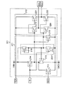
本実施の形態では、本発明の一形態である表示装置について、ブロック図等を参照して説明する。
本実施の形態では、実施の形態1にて説明した表示装置の駆動回路の回路図等について図3乃至図6を参照して説明する。
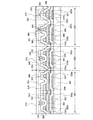
本実施の形態においては、実施の形態1及び実施の形態2に示す表示装置において、論理回路部、スイッチ部、及び画素部の薄膜トランジスタの構造について示す。表示装置に用いる薄膜トランジスタは、p型よりもn型の方が、キャリアの移動度が高い。また、同一の基板上に形成する薄膜トランジスタを全て同じ極性に統一すると、工程数を抑えることができ、好ましい。そのため、本実施の形態では、n型の薄膜トランジスタについて説明する。
ここでは、図7に示す表示装置の作製方法について、図15乃至図18を用いて示す。
本実施の形態では、n型の薄膜トランジスタの作製方法(方法1)について説明する。
または、シリコンまたはゲルマニウムを含む堆積性気体と、水素と、ヘリウム、ネオン、クリプトン等の希ガスとを混合し、グロー放電プラズマにより形成する。シリコンまたはゲルマニウムを含む堆積性気体の流量に対して、水素の流量を10〜2000倍、好ましくは10〜200倍に希釈して、微結晶シリコン、微結晶シリコンゲルマニウム、微結晶ゲルマニウム等を形成する。
ドライエッチングの条件は、露出している第3の半導体層363〜366にダメージが入らず、且つ第3の半導体層363〜366に対するエッチングレートが低い条件を用いる。つまり、露出している第3の半導体層363〜366表面にほとんどダメージを与えず、且つ露出している第3の半導体層363〜366の厚さがほとんど減少しない条件を用いる。エッチングガスとしては、Cl2、CF4、またはN2等を用いる。また、エッチング方法については特に限定はなく、誘導結合型プラズマ(ICP:Inductively Coupled Plasma)方式、容量結合型プラズマ(CCP:Capacitively Coupled Plasma)方式、電子サイクロトン共鳴プラズマ(ECR:Electron Cyclotron Resonance)方式、反応性イオンエッチング(RIE:Reactive Ion Etching)方式等を用いることができる。
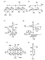
本実施の形態では、本発明の一形態である表示装置に設けられる保護回路について図面を参照して説明する。実施の形態1の図2における保護回路134〜136に用いられる保護回路の具体的な回路構成の例について、図24を参照して説明する。以下の説明ではn型トランジスタを設ける場合についてのみ説明するが、本発明はこれに限定されない。
本実施の形態では、本発明の表示装置の端子部について図25を参照して説明する。
次に、上記実施の形態にて説明した液晶表示装置及び発光表示装置に搭載する表示パネルまたは発光パネルの一形態について、図面(断面図)を参照して説明する。
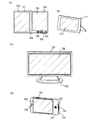
本発明に係る薄膜トランジスタを有する半導体装置は、さまざまな電子機器(遊技機も含む)に適用することができる。電子機器としては、例えば、テレビジョン装置(テレビ、またはテレビジョン受信機ともいう)、コンピュータ用のモニタ、電子ペーパー、デジタルカメラ、デジタルビデオカメラ、デジタルフォトフレーム、携帯電話機(携帯電話、携帯電話装置ともいう)、携帯型ゲーム機、携帯情報端末、音響再生装置、パチンコ機等の大型ゲーム機等が挙げられる。
に示す電子書籍は、電子辞書としての機能を持たせた構成としてもよい。
に示すデジタルフォトフレームは、筐体711に表示部712が組み込まれている。表示部712は、各種画像を表示することが可能であり、例えば、デジタルカメラ等で撮影した画像データを表示させることで、通常の写真立てと同様に機能させることができる。
Claims (2)
- スイッチ部またはバッファ部と、論理回路部と、画素部と、を有し、
前記画素部は、第1のトランジスタと、前記第1のトランジスタに電気的に接続された画素電極と、容量素子と、を有し、
前記スイッチ部またはバッファ部は、第1のゲート電極と第2のゲート電極との間に第1の絶縁層、半導体層、及び第2の絶縁層を有する第2のトランジスタを有し、
前記論理回路部は、第3のトランジスタ及び第4のトランジスタと、配線と、を有し、
前記第1のトランジスタ乃至第4のトランジスタは、同じ極性であり、
前記配線は、前記第3のトランジスタのゲート電極と、前記第3のトランジスタのソース電極又はドレイン電極の一方と、前記第4のトランジスタのソース電極又はドレイン電極の一方と、電気的に接続され、
前記画素電極は、前記容量素子の一方の電極として機能する領域を有し、
前記画素電極と、前記第2のゲート電極と、前記配線とは、同一の導電膜を加工する工程を経て形成されたものであることを特徴とする表示装置。 - 請求項1において、
端子部を有し、
前記端子部は、第1の導電層と、第2の導電層と、第3の導電層と、を有し、
前記第1の導電層は、前記第2の導電層と電気的に接続され、
前記第3の導電層は、前記第1の導電層及び前記第2の導電層の下方に設けられ、フローティングであることを特徴とする表示装置。
Priority Applications (1)
| Application Number | Priority Date | Filing Date | Title |
|---|---|---|---|
| JP2009220148A JP5525224B2 (ja) | 2008-09-30 | 2009-09-25 | 表示装置 |
Applications Claiming Priority (3)
| Application Number | Priority Date | Filing Date | Title |
|---|---|---|---|
| JP2008252418 | 2008-09-30 | ||
| JP2008252418 | 2008-09-30 | ||
| JP2009220148A JP5525224B2 (ja) | 2008-09-30 | 2009-09-25 | 表示装置 |
Related Child Applications (1)
| Application Number | Title | Priority Date | Filing Date |
|---|---|---|---|
| JP2014081688A Division JP5938059B2 (ja) | 2008-09-30 | 2014-04-11 | 表示装置 |
Publications (3)
| Publication Number | Publication Date |
|---|---|
| JP2010109342A JP2010109342A (ja) | 2010-05-13 |
| JP2010109342A5 JP2010109342A5 (ja) | 2012-10-18 |
| JP5525224B2 true JP5525224B2 (ja) | 2014-06-18 |
Family
ID=42056899
Family Applications (11)
| Application Number | Title | Priority Date | Filing Date |
|---|---|---|---|
| JP2009220148A Active JP5525224B2 (ja) | 2008-09-30 | 2009-09-25 | 表示装置 |
| JP2014081688A Active JP5938059B2 (ja) | 2008-09-30 | 2014-04-11 | 表示装置 |
| JP2016059410A Active JP6228253B2 (ja) | 2008-09-30 | 2016-03-24 | 表示装置 |
| JP2017198121A Active JP6480536B2 (ja) | 2008-09-30 | 2017-10-12 | 半導体装置 |
| JP2019020686A Active JP6567786B2 (ja) | 2008-09-30 | 2019-02-07 | 半導体装置、表示装置 |
| JP2019141016A Active JP6661260B2 (ja) | 2008-09-30 | 2019-07-31 | 表示装置 |
| JP2020021058A Active JP6870130B2 (ja) | 2008-09-30 | 2020-02-11 | 表示装置 |
| JP2021068302A Withdrawn JP2021121020A (ja) | 2008-09-30 | 2021-04-14 | 表示装置 |
| JP2022063860A Active JP7250977B2 (ja) | 2008-09-30 | 2022-04-07 | 表示装置 |
| JP2023045302A Active JP7404575B2 (ja) | 2008-09-30 | 2023-03-22 | 表示装置 |
| JP2023209811A Pending JP2024037859A (ja) | 2008-09-30 | 2023-12-13 | 半導体装置及び表示装置 |
Family Applications After (10)
| Application Number | Title | Priority Date | Filing Date |
|---|---|---|---|
| JP2014081688A Active JP5938059B2 (ja) | 2008-09-30 | 2014-04-11 | 表示装置 |
| JP2016059410A Active JP6228253B2 (ja) | 2008-09-30 | 2016-03-24 | 表示装置 |
| JP2017198121A Active JP6480536B2 (ja) | 2008-09-30 | 2017-10-12 | 半導体装置 |
| JP2019020686A Active JP6567786B2 (ja) | 2008-09-30 | 2019-02-07 | 半導体装置、表示装置 |
| JP2019141016A Active JP6661260B2 (ja) | 2008-09-30 | 2019-07-31 | 表示装置 |
| JP2020021058A Active JP6870130B2 (ja) | 2008-09-30 | 2020-02-11 | 表示装置 |
| JP2021068302A Withdrawn JP2021121020A (ja) | 2008-09-30 | 2021-04-14 | 表示装置 |
| JP2022063860A Active JP7250977B2 (ja) | 2008-09-30 | 2022-04-07 | 表示装置 |
| JP2023045302A Active JP7404575B2 (ja) | 2008-09-30 | 2023-03-22 | 表示装置 |
| JP2023209811A Pending JP2024037859A (ja) | 2008-09-30 | 2023-12-13 | 半導体装置及び表示装置 |
Country Status (2)
| Country | Link |
|---|---|
| US (3) | US8284142B2 (ja) |
| JP (11) | JP5525224B2 (ja) |
Families Citing this family (41)
| Publication number | Priority date | Publication date | Assignee | Title |
|---|---|---|---|---|
| JP5436017B2 (ja) * | 2008-04-25 | 2014-03-05 | 株式会社半導体エネルギー研究所 | 半導体装置 |
| KR101602252B1 (ko) * | 2008-06-27 | 2016-03-10 | 가부시키가이샤 한도오따이 에네루기 켄큐쇼 | 박막 트랜지스터, 반도체장치 및 전자기기 |
| JP5590868B2 (ja) * | 2008-12-11 | 2014-09-17 | 株式会社半導体エネルギー研究所 | 半導体装置 |
| KR101721285B1 (ko) * | 2009-10-09 | 2017-03-29 | 가부시키가이샤 한도오따이 에네루기 켄큐쇼 | 시프트 레지스터 및 표시 장치 |
| KR101943293B1 (ko) * | 2009-10-16 | 2019-01-29 | 가부시키가이샤 한도오따이 에네루기 켄큐쇼 | 반도체 장치, 표시 장치 및 전자 장치 |
| US20140132861A1 (en) * | 2010-05-31 | 2014-05-15 | Wintek Corporation | Touch panel and touch-sensitive display device |
| WO2011151955A1 (ja) * | 2010-05-31 | 2011-12-08 | シャープ株式会社 | 半導体素子、薄膜トランジスタ基板及び表示装置 |
| US8735231B2 (en) * | 2010-08-26 | 2014-05-27 | Semiconductor Energy Laboratory Co., Ltd. | Manufacturing method of dual-gate thin film transistor |
| KR20120060407A (ko) * | 2010-12-02 | 2012-06-12 | 삼성전자주식회사 | 표시 기판, 이의 제조 방법 및 이를 포함하는 터치 표시 장치 |
| KR101843871B1 (ko) * | 2011-03-11 | 2018-04-02 | 삼성디스플레이 주식회사 | 박막 트랜지스터 표시판 및 그 제조 방법 |
| US8878174B2 (en) * | 2011-04-15 | 2014-11-04 | Semiconductor Energy Laboratory Co., Ltd. | Semiconductor element, memory circuit, integrated circuit, and driving method of the integrated circuit |
| TWI792087B (zh) | 2011-05-05 | 2023-02-11 | 日商半導體能源研究所股份有限公司 | 半導體裝置及其製造方法 |
| JP5931573B2 (ja) * | 2011-05-13 | 2016-06-08 | 株式会社半導体エネルギー研究所 | 半導体装置の作製方法 |
| GB2492442B (en) * | 2011-06-27 | 2015-11-04 | Pragmatic Printing Ltd | Transistor and its method of manufacture |
| JP6050054B2 (ja) * | 2011-09-09 | 2016-12-21 | 株式会社半導体エネルギー研究所 | 半導体装置 |
| US8698137B2 (en) * | 2011-09-14 | 2014-04-15 | Semiconductor Energy Laboratory Co., Ltd. | Semiconductor device |
| CN102646676B (zh) * | 2011-11-03 | 2015-06-10 | 京东方科技集团股份有限公司 | 一种tft阵列基板 |
| TW201340181A (zh) * | 2012-03-30 | 2013-10-01 | Chunghwa Picture Tubes Ltd | 觸控面板及其觸碰感應層的製造方法 |
| US10541183B2 (en) * | 2012-07-19 | 2020-01-21 | Texas Instruments Incorporated | Spectral reflectometry window heater |
| JP2014045175A (ja) | 2012-08-02 | 2014-03-13 | Semiconductor Energy Lab Co Ltd | 半導体装置 |
| JP6300589B2 (ja) | 2013-04-04 | 2018-03-28 | 株式会社半導体エネルギー研究所 | 半導体装置の作製方法 |
| US20140374744A1 (en) | 2013-06-19 | 2014-12-25 | Semiconductor Energy Laboratory Co., Ltd. | Semiconductor device |
| JP6490914B2 (ja) * | 2013-06-28 | 2019-03-27 | 株式会社半導体エネルギー研究所 | 半導体装置の作製方法 |
| JP6397654B2 (ja) * | 2014-05-13 | 2018-09-26 | 株式会社ジャパンディスプレイ | 有機el発光装置 |
| JP6360718B2 (ja) | 2014-05-16 | 2018-07-18 | 株式会社ジャパンディスプレイ | 表示装置 |
| WO2016034984A1 (en) * | 2014-09-05 | 2016-03-10 | Semiconductor Energy Laboratory Co., Ltd. | Semiconductor device, driver ic, display device, and electronic device |
| WO2016076168A1 (ja) * | 2014-11-11 | 2016-05-19 | シャープ株式会社 | 半導体装置およびその製造方法 |
| CN105140291B (zh) * | 2015-07-13 | 2019-01-15 | 京东方科技集团股份有限公司 | 薄膜晶体管及其制作方法、阵列基板以及显示装置 |
| US9935127B2 (en) * | 2015-07-29 | 2018-04-03 | Wuhan China Star Optoelectronics Technology Co., Ltd. | Control circuit of thin film transistor |
| CN105807523B (zh) * | 2016-05-27 | 2020-03-20 | 厦门天马微电子有限公司 | 阵列基板、包含其的显示面板和显示装置 |
| CN106020554A (zh) * | 2016-06-06 | 2016-10-12 | 京东方科技集团股份有限公司 | 触控盖板及其制造方法和触控显示装置 |
| CN106444183B (zh) * | 2016-12-09 | 2019-12-31 | 深圳市华星光电技术有限公司 | 一种超窄边框端子区结构及制作方法、显示面板 |
| US11302718B2 (en) | 2017-05-18 | 2022-04-12 | Sharp Kabushiki Kaisha | Active matrix substrate and production method therefor |
| US10559596B2 (en) * | 2018-03-23 | 2020-02-11 | Innolux Corporation | Display device |
| US11139562B2 (en) * | 2018-09-14 | 2021-10-05 | Innolux Corporation | Antenna device |
| CN110911382B (zh) * | 2018-09-14 | 2021-06-25 | 群创光电股份有限公司 | 天线装置 |
| CN111223459B (zh) | 2018-11-27 | 2022-03-08 | 元太科技工业股份有限公司 | 移位寄存器以及栅极驱动电路 |
| CN110010078B (zh) * | 2019-03-14 | 2022-02-08 | 合肥京东方卓印科技有限公司 | 移位寄存器单元、栅极驱动电路和显示装置 |
| CN112086424B (zh) * | 2019-06-14 | 2023-06-23 | 群创光电股份有限公司 | 接合垫结构 |
| CN111552132A (zh) * | 2020-03-31 | 2020-08-18 | 浙江大学 | 一种应用在投影面板上的像素结构及投影面板 |
| CN112530937B (zh) * | 2020-12-02 | 2022-09-27 | Tcl华星光电技术有限公司 | 一种静电保护电路和显示面板 |
Family Cites Families (83)
| Publication number | Priority date | Publication date | Assignee | Title |
|---|---|---|---|---|
| JPS56122123A (en) | 1980-03-03 | 1981-09-25 | Shunpei Yamazaki | Semiamorphous semiconductor |
| JPH03294824A (ja) * | 1990-04-13 | 1991-12-26 | Nec Corp | アクティブマトリックス型液晶表示素子アレイ |
| DE69112698T2 (de) * | 1990-05-07 | 1996-02-15 | Fujitsu Ltd | Anzeigeeinrichtung von höher Qualität mit aktiver Matrix. |
| US5849601A (en) | 1990-12-25 | 1998-12-15 | Semiconductor Energy Laboratory Co., Ltd. | Electro-optical device and method for manufacturing the same |
| JP3107312B2 (ja) * | 1990-11-28 | 2000-11-06 | シャープ株式会社 | アクティブマトリクス表示装置 |
| JP2776083B2 (ja) * | 1991-08-23 | 1998-07-16 | 日本電気株式会社 | 液晶表示装置およびその製造方法 |
| JPH07114045A (ja) | 1993-10-19 | 1995-05-02 | Sanyo Electric Co Ltd | 液晶表示装置 |
| US6747627B1 (en) | 1994-04-22 | 2004-06-08 | Semiconductor Energy Laboratory Co., Ltd. | Redundancy shift register circuit for driver circuit in active matrix type liquid crystal display device |
| JP3402400B2 (ja) | 1994-04-22 | 2003-05-06 | 株式会社半導体エネルギー研究所 | 半導体集積回路の作製方法 |
| WO1997005659A1 (en) | 1995-07-31 | 1997-02-13 | Litton Systems Canada Limited | Flat panel detector for radiation imaging with reduced trapped charges |
| JP3514002B2 (ja) * | 1995-09-04 | 2004-03-31 | カシオ計算機株式会社 | 表示駆動装置 |
| CN100414411C (zh) | 1995-10-03 | 2008-08-27 | 精工爱普生株式会社 | 有源矩阵基板的制造方法和薄膜元件的制造方法 |
| TW328641B (en) | 1995-12-04 | 1998-03-21 | Hitachi Ltd | Semiconductor integrated circuit device and process for producing the same |
| TW335503B (en) | 1996-02-23 | 1998-07-01 | Semiconductor Energy Lab Kk | Semiconductor thin film and manufacturing method and semiconductor device and its manufacturing method |
| US5986724A (en) * | 1996-03-01 | 1999-11-16 | Kabushiki Kaisha Toshiba | Liquid crystal display with liquid crystal layer and ferroelectric layer connected to drain of TFT |
| JPH09281508A (ja) | 1996-04-12 | 1997-10-31 | Semiconductor Energy Lab Co Ltd | 液晶表示装置およびその作製方法 |
| JPH10198292A (ja) | 1996-12-30 | 1998-07-31 | Semiconductor Energy Lab Co Ltd | 半導体装置およびその作製方法 |
| JPH10332494A (ja) | 1997-06-03 | 1998-12-18 | Oki Data:Kk | 温度検出回路、駆動装置及びプリンタ |
| JPH10340070A (ja) | 1997-06-09 | 1998-12-22 | Hitachi Ltd | 液晶表示装置 |
| JP3464599B2 (ja) * | 1997-10-06 | 2003-11-10 | 株式会社 日立ディスプレイズ | 液晶表示装置 |
| JP4044187B2 (ja) | 1997-10-20 | 2008-02-06 | 株式会社半導体エネルギー研究所 | アクティブマトリクス型表示装置およびその作製方法 |
| JP3820743B2 (ja) | 1998-03-30 | 2006-09-13 | セイコーエプソン株式会社 | アクティブマトリクス基板およびアクティブマトリクス基板の製造方法および表示装置 |
| GB9812739D0 (en) * | 1998-06-12 | 1998-08-12 | Koninkl Philips Electronics Nv | Active matrix electroluminescent display devices |
| US6297519B1 (en) | 1998-08-28 | 2001-10-02 | Fujitsu Limited | TFT substrate with low contact resistance and damage resistant terminals |
| US7126161B2 (en) | 1998-10-13 | 2006-10-24 | Semiconductor Energy Laboratory Co., Ltd. | Semiconductor device having El layer and sealing material |
| US6274887B1 (en) | 1998-11-02 | 2001-08-14 | Semiconductor Energy Laboratory Co., Ltd. | Semiconductor device and manufacturing method therefor |
| JP2000174282A (ja) | 1998-12-03 | 2000-06-23 | Semiconductor Energy Lab Co Ltd | 半導体装置 |
| US6469317B1 (en) | 1998-12-18 | 2002-10-22 | Semiconductor Energy Laboratory Co., Ltd. | Semiconductor device and method of fabricating the same |
| TW461180B (en) * | 1998-12-21 | 2001-10-21 | Sony Corp | Digital/analog converter circuit, level shift circuit, shift register utilizing level shift circuit, sampling latch circuit, latch circuit and liquid crystal display device incorporating the same |
| US6593592B1 (en) | 1999-01-29 | 2003-07-15 | Semiconductor Energy Laboratory Co., Ltd. | Semiconductor device having thin film transistors |
| US6858898B1 (en) | 1999-03-23 | 2005-02-22 | Semiconductor Energy Laboratory Co., Ltd. | Semiconductor device and method for manufacturing the same |
| JP4651773B2 (ja) * | 1999-04-06 | 2011-03-16 | 株式会社半導体エネルギー研究所 | 半導体装置の作製方法 |
| JP4307635B2 (ja) | 1999-06-22 | 2009-08-05 | 株式会社半導体エネルギー研究所 | 半導体装置の作製方法 |
| JP2001102587A (ja) * | 1999-09-28 | 2001-04-13 | Toshiba Corp | 薄膜トランジスタおよびその製造方法ならびに半導体薄膜の製造方法 |
| TW493152B (en) | 1999-12-24 | 2002-07-01 | Semiconductor Energy Lab | Electronic device |
| US7023021B2 (en) | 2000-02-22 | 2006-04-04 | Semiconductor Energy Laboratory Co., Ltd. | Semiconductor device and method of manufacturing the same |
| TW507258B (en) | 2000-02-29 | 2002-10-21 | Semiconductor Systems Corp | Display device and method for fabricating the same |
| TW521226B (en) * | 2000-03-27 | 2003-02-21 | Semiconductor Energy Lab | Electro-optical device |
| GB0008019D0 (en) * | 2000-03-31 | 2000-05-17 | Koninkl Philips Electronics Nv | Display device having current-addressed pixels |
| JP2002032057A (ja) * | 2000-05-08 | 2002-01-31 | Semiconductor Energy Lab Co Ltd | 発光装置及びその駆動方法 |
| JP5183838B2 (ja) | 2000-05-12 | 2013-04-17 | 株式会社半導体エネルギー研究所 | 発光装置 |
| US7633471B2 (en) | 2000-05-12 | 2009-12-15 | Semiconductor Energy Laboratory Co., Ltd. | Light-emitting device and electric appliance |
| TW536827B (en) * | 2000-07-14 | 2003-06-11 | Semiconductor Energy Lab | Semiconductor display apparatus and driving method of semiconductor display apparatus |
| JP4993826B2 (ja) * | 2000-08-14 | 2012-08-08 | 株式会社半導体エネルギー研究所 | 半導体装置の作製方法 |
| JP4761681B2 (ja) * | 2000-10-05 | 2011-08-31 | 株式会社半導体エネルギー研究所 | 液晶表示装置 |
| JP2002175053A (ja) * | 2000-12-07 | 2002-06-21 | Sony Corp | アクティブマトリクス型表示装置およびこれを用いた携帯端末 |
| JP4501048B2 (ja) * | 2000-12-28 | 2010-07-14 | カシオ計算機株式会社 | シフトレジスタ回路及びその駆動制御方法並びに表示駆動装置、読取駆動装置 |
| JP4079655B2 (ja) * | 2001-02-28 | 2008-04-23 | 株式会社半導体エネルギー研究所 | 半導体装置およびその作製方法 |
| SG118117A1 (en) | 2001-02-28 | 2006-01-27 | Semiconductor Energy Lab | Semiconductor device and manufacturing method thereof |
| TW575777B (en) | 2001-03-30 | 2004-02-11 | Sanyo Electric Co | Active matrix type display device |
| JP2002297059A (ja) * | 2001-03-30 | 2002-10-09 | Sanyo Electric Co Ltd | ドライバ内蔵型アクティブマトリクス表示装置 |
| JP2003069028A (ja) * | 2001-08-27 | 2003-03-07 | Casio Comput Co Ltd | 薄膜トランジスタパネル |
| CN101257743B (zh) * | 2001-08-29 | 2011-05-25 | 株式会社半导体能源研究所 | 发光器件及这种发光器件的驱动方法 |
| JP2003273361A (ja) * | 2002-03-15 | 2003-09-26 | Sharp Corp | 半導体装置およびその製造方法 |
| US7023410B2 (en) | 2002-04-08 | 2006-04-04 | Samsung Electronics Co., Ltd. | Liquid crystal display device |
| JP3776890B2 (ja) * | 2003-02-12 | 2006-05-17 | 日本電気株式会社 | 表示装置の駆動回路 |
| JP4748954B2 (ja) | 2003-07-14 | 2011-08-17 | 株式会社半導体エネルギー研究所 | 液晶表示装置 |
| JP4698998B2 (ja) * | 2004-09-30 | 2011-06-08 | 株式会社半導体エネルギー研究所 | 液晶表示装置の作製方法 |
| KR101066493B1 (ko) * | 2004-12-31 | 2011-09-21 | 엘지디스플레이 주식회사 | 쉬프트 레지스터 |
| JP2006293344A (ja) * | 2005-03-18 | 2006-10-26 | Semiconductor Energy Lab Co Ltd | 半導体装置、表示装置及びその駆動方法並びに電子機器 |
| US8681077B2 (en) | 2005-03-18 | 2014-03-25 | Semiconductor Energy Laboratory Co., Ltd. | Semiconductor device, and display device, driving method and electronic apparatus thereof |
| JP5064747B2 (ja) * | 2005-09-29 | 2012-10-31 | 株式会社半導体エネルギー研究所 | 半導体装置、電気泳動表示装置、表示モジュール、電子機器、及び半導体装置の作製方法 |
| KR101154338B1 (ko) | 2006-02-15 | 2012-06-13 | 삼성전자주식회사 | 쉬프트 레지스터와, 이를 갖는 스캔 구동 회로 및 표시장치 |
| JP2007286266A (ja) * | 2006-04-14 | 2007-11-01 | Toshiba Matsushita Display Technology Co Ltd | 表示駆動装置、平面表示装置及び表示駆動方法 |
| JP5386069B2 (ja) * | 2006-06-02 | 2014-01-15 | 株式会社半導体エネルギー研究所 | 半導体装置、表示装置、液晶表示装置、表示モジュール及び電子機器 |
| TWI342544B (en) * | 2006-06-30 | 2011-05-21 | Wintek Corp | Shift register |
| KR101254644B1 (ko) * | 2006-06-30 | 2013-04-15 | 엘지디스플레이 주식회사 | 유기 전계발광 표시장치와 그의 제조 방법 |
| KR20080002338A (ko) * | 2006-06-30 | 2008-01-04 | 엘지.필립스 엘시디 주식회사 | 유기 전계발광 표시장치와 그의 제조 방법 |
| JP5116277B2 (ja) * | 2006-09-29 | 2013-01-09 | 株式会社半導体エネルギー研究所 | 半導体装置、表示装置、液晶表示装置、表示モジュール及び電子機器 |
| JP4932415B2 (ja) * | 2006-09-29 | 2012-05-16 | 株式会社半導体エネルギー研究所 | 半導体装置 |
| JP2008140489A (ja) * | 2006-12-04 | 2008-06-19 | Seiko Epson Corp | シフトレジスタ、走査線駆動回路、データ線駆動回路、電気光学装置及び電子機器 |
| JP4867657B2 (ja) * | 2006-12-28 | 2012-02-01 | ソニー株式会社 | 電圧供給回路、表示装置、および電子機器、並びに電圧供給方法 |
| JP4912186B2 (ja) * | 2007-03-05 | 2012-04-11 | 三菱電機株式会社 | シフトレジスタ回路およびそれを備える画像表示装置 |
| JP5512930B2 (ja) * | 2007-03-26 | 2014-06-04 | 株式会社半導体エネルギー研究所 | 半導体装置の作製方法 |
| JP5512931B2 (ja) * | 2007-03-26 | 2014-06-04 | 株式会社半導体エネルギー研究所 | 半導体装置の作製方法 |
| KR101427577B1 (ko) * | 2007-09-06 | 2014-08-08 | 삼성디스플레이 주식회사 | 전기 영동 표시 장치 및 전기 영동 표시 장치의 구동 방법 |
| US8138032B2 (en) | 2008-04-18 | 2012-03-20 | Semiconductor Energy Laboratory Co., Ltd. | Method for manufacturing thin film transistor having microcrystalline semiconductor film |
| WO2009157574A1 (en) | 2008-06-27 | 2009-12-30 | Semiconductor Energy Laboratory Co., Ltd. | Thin film transistor |
| KR101622981B1 (ko) | 2008-09-19 | 2016-05-20 | 가부시키가이샤 한도오따이 에네루기 켄큐쇼 | 표시장치 및 그 제조방법 |
| TWI574423B (zh) | 2008-11-07 | 2017-03-11 | 半導體能源研究所股份有限公司 | 半導體裝置和其製造方法 |
| JP5498762B2 (ja) | 2008-11-17 | 2014-05-21 | 株式会社半導体エネルギー研究所 | 薄膜トランジスタの作製方法 |
| JP5590868B2 (ja) | 2008-12-11 | 2014-09-17 | 株式会社半導体エネルギー研究所 | 半導体装置 |
| KR101740943B1 (ko) | 2009-09-24 | 2017-06-15 | 가부시키가이샤 한도오따이 에네루기 켄큐쇼 | 표시 장치 |
-
2009
- 2009-09-25 US US12/567,413 patent/US8284142B2/en not_active Expired - Fee Related
- 2009-09-25 JP JP2009220148A patent/JP5525224B2/ja active Active
-
2012
- 2012-09-13 US US13/613,811 patent/US9048147B2/en not_active Expired - Fee Related
-
2014
- 2014-04-11 JP JP2014081688A patent/JP5938059B2/ja active Active
-
2015
- 2015-05-13 US US14/711,275 patent/US9563094B2/en active Active
-
2016
- 2016-03-24 JP JP2016059410A patent/JP6228253B2/ja active Active
-
2017
- 2017-10-12 JP JP2017198121A patent/JP6480536B2/ja active Active
-
2019
- 2019-02-07 JP JP2019020686A patent/JP6567786B2/ja active Active
- 2019-07-31 JP JP2019141016A patent/JP6661260B2/ja active Active
-
2020
- 2020-02-11 JP JP2020021058A patent/JP6870130B2/ja active Active
-
2021
- 2021-04-14 JP JP2021068302A patent/JP2021121020A/ja not_active Withdrawn
-
2022
- 2022-04-07 JP JP2022063860A patent/JP7250977B2/ja active Active
-
2023
- 2023-03-22 JP JP2023045302A patent/JP7404575B2/ja active Active
- 2023-12-13 JP JP2023209811A patent/JP2024037859A/ja active Pending
Also Published As
| Publication number | Publication date |
|---|---|
| US20150323823A1 (en) | 2015-11-12 |
| JP2023099365A (ja) | 2023-07-12 |
| US9048147B2 (en) | 2015-06-02 |
| US9563094B2 (en) | 2017-02-07 |
| JP6480536B2 (ja) | 2019-03-13 |
| US20130002624A1 (en) | 2013-01-03 |
| JP6661260B2 (ja) | 2020-03-11 |
| US8284142B2 (en) | 2012-10-09 |
| JP2014179627A (ja) | 2014-09-25 |
| JP6567786B2 (ja) | 2019-08-28 |
| JP6870130B2 (ja) | 2021-05-12 |
| JP2018022185A (ja) | 2018-02-08 |
| JP6228253B2 (ja) | 2017-11-08 |
| JP2021121020A (ja) | 2021-08-19 |
| JP7250977B2 (ja) | 2023-04-03 |
| JP2022115858A (ja) | 2022-08-09 |
| JP2016154245A (ja) | 2016-08-25 |
| JP5938059B2 (ja) | 2016-06-22 |
| JP2010109342A (ja) | 2010-05-13 |
| US20100079425A1 (en) | 2010-04-01 |
| JP2019124944A (ja) | 2019-07-25 |
| JP7404575B2 (ja) | 2023-12-25 |
| JP2019200431A (ja) | 2019-11-21 |
| JP2024037859A (ja) | 2024-03-19 |
| JP2020109516A (ja) | 2020-07-16 |
Similar Documents
| Publication | Publication Date | Title |
|---|---|---|
| JP6567786B2 (ja) | 半導体装置、表示装置 | |
| US11024516B2 (en) | Display device and method for manufacturing the same | |
| JP5562603B2 (ja) | 表示装置 | |
| JP6567711B2 (ja) | 表示装置 | |
| JP2020095278A (ja) | 半導体装置 | |
| JP5632654B2 (ja) | 表示装置 |
Legal Events
| Date | Code | Title | Description |
|---|---|---|---|
| A521 | Request for written amendment filed |
Free format text: JAPANESE INTERMEDIATE CODE: A523 Effective date: 20120905 |
|
| A621 | Written request for application examination |
Free format text: JAPANESE INTERMEDIATE CODE: A621 Effective date: 20120905 |
|
| A131 | Notification of reasons for refusal |
Free format text: JAPANESE INTERMEDIATE CODE: A131 Effective date: 20131015 |
|
| A521 | Request for written amendment filed |
Free format text: JAPANESE INTERMEDIATE CODE: A523 Effective date: 20131030 |
|
| TRDD | Decision of grant or rejection written | ||
| A01 | Written decision to grant a patent or to grant a registration (utility model) |
Free format text: JAPANESE INTERMEDIATE CODE: A01 Effective date: 20140318 |
|
| A61 | First payment of annual fees (during grant procedure) |
Free format text: JAPANESE INTERMEDIATE CODE: A61 Effective date: 20140411 |
|
| R150 | Certificate of patent or registration of utility model |
Ref document number: 5525224 Country of ref document: JP Free format text: JAPANESE INTERMEDIATE CODE: R150 |
|
| R250 | Receipt of annual fees |
Free format text: JAPANESE INTERMEDIATE CODE: R250 |
|
| R250 | Receipt of annual fees |
Free format text: JAPANESE INTERMEDIATE CODE: R250 |
|
| R250 | Receipt of annual fees |
Free format text: JAPANESE INTERMEDIATE CODE: R250 |
|
| R250 | Receipt of annual fees |
Free format text: JAPANESE INTERMEDIATE CODE: R250 |
|
| R250 | Receipt of annual fees |
Free format text: JAPANESE INTERMEDIATE CODE: R250 |
|
| R250 | Receipt of annual fees |
Free format text: JAPANESE INTERMEDIATE CODE: R250 |
|
| R250 | Receipt of annual fees |
Free format text: JAPANESE INTERMEDIATE CODE: R250 |
|
| R250 | Receipt of annual fees |
Free format text: JAPANESE INTERMEDIATE CODE: R250 |