JP5352081B2 - 半導体装置の作製方法 - Google Patents
半導体装置の作製方法 Download PDFInfo
- Publication number
- JP5352081B2 JP5352081B2 JP2007315322A JP2007315322A JP5352081B2 JP 5352081 B2 JP5352081 B2 JP 5352081B2 JP 2007315322 A JP2007315322 A JP 2007315322A JP 2007315322 A JP2007315322 A JP 2007315322A JP 5352081 B2 JP5352081 B2 JP 5352081B2
- Authority
- JP
- Japan
- Prior art keywords
- film
- region
- gate electrode
- insulating film
- concentration impurity
- Prior art date
- Legal status (The legal status is an assumption and is not a legal conclusion. Google has not performed a legal analysis and makes no representation as to the accuracy of the status listed.)
- Expired - Fee Related
Links
- 239000004065 semiconductor Substances 0.000 title claims abstract description 152
- 238000000034 method Methods 0.000 title description 45
- 238000004519 manufacturing process Methods 0.000 title description 20
- 239000012535 impurity Substances 0.000 claims abstract description 215
- 238000005530 etching Methods 0.000 claims description 61
- 239000000758 substrate Substances 0.000 claims description 46
- 230000015572 biosynthetic process Effects 0.000 claims description 33
- 229910021332 silicide Inorganic materials 0.000 abstract description 36
- FVBUAEGBCNSCDD-UHFFFAOYSA-N silicide(4-) Chemical compound [Si-4] FVBUAEGBCNSCDD-UHFFFAOYSA-N 0.000 abstract description 36
- 239000010408 film Substances 0.000 description 402
- 239000010410 layer Substances 0.000 description 86
- 239000011229 interlayer Substances 0.000 description 32
- 229910052751 metal Inorganic materials 0.000 description 24
- 239000002184 metal Substances 0.000 description 24
- 239000007789 gas Substances 0.000 description 23
- OAICVXFJPJFONN-UHFFFAOYSA-N Phosphorus Chemical compound [P] OAICVXFJPJFONN-UHFFFAOYSA-N 0.000 description 19
- 229910052698 phosphorus Inorganic materials 0.000 description 19
- 239000011574 phosphorus Substances 0.000 description 19
- 239000010409 thin film Substances 0.000 description 19
- IJGRMHOSHXDMSA-UHFFFAOYSA-N Atomic nitrogen Chemical compound N#N IJGRMHOSHXDMSA-UHFFFAOYSA-N 0.000 description 18
- VYPSYNLAJGMNEJ-UHFFFAOYSA-N silicon dioxide Inorganic materials O=[Si]=O VYPSYNLAJGMNEJ-UHFFFAOYSA-N 0.000 description 18
- 229910052814 silicon oxide Inorganic materials 0.000 description 17
- PXHVJJICTQNCMI-UHFFFAOYSA-N Nickel Chemical compound [Ni] PXHVJJICTQNCMI-UHFFFAOYSA-N 0.000 description 14
- 239000010936 titanium Substances 0.000 description 14
- 229910052782 aluminium Inorganic materials 0.000 description 12
- XAGFODPZIPBFFR-UHFFFAOYSA-N aluminium Chemical compound [Al] XAGFODPZIPBFFR-UHFFFAOYSA-N 0.000 description 12
- 238000010438 heat treatment Methods 0.000 description 11
- 238000010586 diagram Methods 0.000 description 10
- 229910052581 Si3N4 Inorganic materials 0.000 description 9
- RTAQQCXQSZGOHL-UHFFFAOYSA-N Titanium Chemical compound [Ti] RTAQQCXQSZGOHL-UHFFFAOYSA-N 0.000 description 9
- 239000010949 copper Substances 0.000 description 9
- 230000006870 function Effects 0.000 description 9
- 229910052757 nitrogen Inorganic materials 0.000 description 9
- HQVNEWCFYHHQES-UHFFFAOYSA-N silicon nitride Chemical compound N12[Si]34N5[Si]62N3[Si]51N64 HQVNEWCFYHHQES-UHFFFAOYSA-N 0.000 description 9
- 229910052719 titanium Inorganic materials 0.000 description 9
- 230000004888 barrier function Effects 0.000 description 8
- 239000013078 crystal Substances 0.000 description 8
- XKRFYHLGVUSROY-UHFFFAOYSA-N Argon Chemical compound [Ar] XKRFYHLGVUSROY-UHFFFAOYSA-N 0.000 description 7
- 229910052759 nickel Inorganic materials 0.000 description 7
- RYGMFSIKBFXOCR-UHFFFAOYSA-N Copper Chemical compound [Cu] RYGMFSIKBFXOCR-UHFFFAOYSA-N 0.000 description 6
- QVGXLLKOCUKJST-UHFFFAOYSA-N atomic oxygen Chemical compound [O] QVGXLLKOCUKJST-UHFFFAOYSA-N 0.000 description 6
- 229910052802 copper Inorganic materials 0.000 description 6
- 230000006866 deterioration Effects 0.000 description 6
- 239000001301 oxygen Substances 0.000 description 6
- 229910052760 oxygen Inorganic materials 0.000 description 6
- 230000008569 process Effects 0.000 description 6
- 239000002356 single layer Substances 0.000 description 6
- MZLGASXMSKOWSE-UHFFFAOYSA-N tantalum nitride Chemical compound [Ta]#N MZLGASXMSKOWSE-UHFFFAOYSA-N 0.000 description 6
- XUIMIQQOPSSXEZ-UHFFFAOYSA-N Silicon Chemical compound [Si] XUIMIQQOPSSXEZ-UHFFFAOYSA-N 0.000 description 5
- 239000000956 alloy Substances 0.000 description 5
- 239000011651 chromium Substances 0.000 description 5
- 239000000463 material Substances 0.000 description 5
- 239000011368 organic material Substances 0.000 description 5
- 238000000206 photolithography Methods 0.000 description 5
- 229910052710 silicon Inorganic materials 0.000 description 5
- 239000010703 silicon Substances 0.000 description 5
- WFKWXMTUELFFGS-UHFFFAOYSA-N tungsten Chemical compound [W] WFKWXMTUELFFGS-UHFFFAOYSA-N 0.000 description 5
- 229910052721 tungsten Inorganic materials 0.000 description 5
- 239000010937 tungsten Substances 0.000 description 5
- ZOXJGFHDIHLPTG-UHFFFAOYSA-N Boron Chemical compound [B] ZOXJGFHDIHLPTG-UHFFFAOYSA-N 0.000 description 4
- 229910021417 amorphous silicon Inorganic materials 0.000 description 4
- 238000004458 analytical method Methods 0.000 description 4
- 229910052786 argon Inorganic materials 0.000 description 4
- 229910052796 boron Inorganic materials 0.000 description 4
- 238000002425 crystallisation Methods 0.000 description 4
- 230000000694 effects Effects 0.000 description 4
- 239000001257 hydrogen Substances 0.000 description 4
- 229910052739 hydrogen Inorganic materials 0.000 description 4
- 150000002500 ions Chemical class 0.000 description 4
- 239000007788 liquid Substances 0.000 description 4
- 239000004033 plastic Substances 0.000 description 4
- 229920003023 plastic Polymers 0.000 description 4
- BASFCYQUMIYNBI-UHFFFAOYSA-N platinum Chemical compound [Pt] BASFCYQUMIYNBI-UHFFFAOYSA-N 0.000 description 4
- 229920005989 resin Polymers 0.000 description 4
- 239000011347 resin Substances 0.000 description 4
- 239000007787 solid Substances 0.000 description 4
- 229910052715 tantalum Inorganic materials 0.000 description 4
- GUVRBAGPIYLISA-UHFFFAOYSA-N tantalum atom Chemical compound [Ta] GUVRBAGPIYLISA-UHFFFAOYSA-N 0.000 description 4
- 102100040844 Dual specificity protein kinase CLK2 Human genes 0.000 description 3
- 101000749291 Homo sapiens Dual specificity protein kinase CLK2 Proteins 0.000 description 3
- UFHFLCQGNIYNRP-UHFFFAOYSA-N Hydrogen Chemical compound [H][H] UFHFLCQGNIYNRP-UHFFFAOYSA-N 0.000 description 3
- ZOKXTWBITQBERF-UHFFFAOYSA-N Molybdenum Chemical compound [Mo] ZOKXTWBITQBERF-UHFFFAOYSA-N 0.000 description 3
- XYFCBTPGUUZFHI-UHFFFAOYSA-N Phosphine Chemical compound P XYFCBTPGUUZFHI-UHFFFAOYSA-N 0.000 description 3
- 229910020286 SiOxNy Inorganic materials 0.000 description 3
- 229910045601 alloy Inorganic materials 0.000 description 3
- -1 argon ion Chemical class 0.000 description 3
- 125000004429 atom Chemical group 0.000 description 3
- 239000000969 carrier Substances 0.000 description 3
- 230000008025 crystallization Effects 0.000 description 3
- 230000005684 electric field Effects 0.000 description 3
- 229910010272 inorganic material Inorganic materials 0.000 description 3
- 239000011147 inorganic material Substances 0.000 description 3
- 229910052743 krypton Inorganic materials 0.000 description 3
- DNNSSWSSYDEUBZ-UHFFFAOYSA-N krypton atom Chemical compound [Kr] DNNSSWSSYDEUBZ-UHFFFAOYSA-N 0.000 description 3
- 229910052750 molybdenum Inorganic materials 0.000 description 3
- 239000011733 molybdenum Substances 0.000 description 3
- 230000002040 relaxant effect Effects 0.000 description 3
- SBEQWOXEGHQIMW-UHFFFAOYSA-N silicon Chemical compound [Si].[Si] SBEQWOXEGHQIMW-UHFFFAOYSA-N 0.000 description 3
- OKTJSMMVPCPJKN-UHFFFAOYSA-N Carbon Chemical compound [C] OKTJSMMVPCPJKN-UHFFFAOYSA-N 0.000 description 2
- CURLTUGMZLYLDI-UHFFFAOYSA-N Carbon dioxide Chemical compound O=C=O CURLTUGMZLYLDI-UHFFFAOYSA-N 0.000 description 2
- VYZAMTAEIAYCRO-UHFFFAOYSA-N Chromium Chemical compound [Cr] VYZAMTAEIAYCRO-UHFFFAOYSA-N 0.000 description 2
- 102100040862 Dual specificity protein kinase CLK1 Human genes 0.000 description 2
- GYHNNYVSQQEPJS-UHFFFAOYSA-N Gallium Chemical compound [Ga] GYHNNYVSQQEPJS-UHFFFAOYSA-N 0.000 description 2
- 101000749294 Homo sapiens Dual specificity protein kinase CLK1 Proteins 0.000 description 2
- 229910004286 SiNxOy Inorganic materials 0.000 description 2
- BQCADISMDOOEFD-UHFFFAOYSA-N Silver Chemical compound [Ag] BQCADISMDOOEFD-UHFFFAOYSA-N 0.000 description 2
- NRTOMJZYCJJWKI-UHFFFAOYSA-N Titanium nitride Chemical compound [Ti]#N NRTOMJZYCJJWKI-UHFFFAOYSA-N 0.000 description 2
- 229910052785 arsenic Inorganic materials 0.000 description 2
- RQNWIZPPADIBDY-UHFFFAOYSA-N arsenic atom Chemical compound [As] RQNWIZPPADIBDY-UHFFFAOYSA-N 0.000 description 2
- GPBUGPUPKAGMDK-UHFFFAOYSA-N azanylidynemolybdenum Chemical compound [Mo]#N GPBUGPUPKAGMDK-UHFFFAOYSA-N 0.000 description 2
- 229910052799 carbon Inorganic materials 0.000 description 2
- 230000015556 catabolic process Effects 0.000 description 2
- 230000008859 change Effects 0.000 description 2
- 239000013522 chelant Substances 0.000 description 2
- 229910052804 chromium Inorganic materials 0.000 description 2
- 229910017052 cobalt Inorganic materials 0.000 description 2
- 239000010941 cobalt Substances 0.000 description 2
- GUTLYIVDDKVIGB-UHFFFAOYSA-N cobalt atom Chemical compound [Co] GUTLYIVDDKVIGB-UHFFFAOYSA-N 0.000 description 2
- 150000001875 compounds Chemical class 0.000 description 2
- 229910021419 crystalline silicon Inorganic materials 0.000 description 2
- 238000000354 decomposition reaction Methods 0.000 description 2
- 239000003822 epoxy resin Substances 0.000 description 2
- 238000000605 extraction Methods 0.000 description 2
- 229910052733 gallium Inorganic materials 0.000 description 2
- 239000011521 glass Substances 0.000 description 2
- 229910052736 halogen Inorganic materials 0.000 description 2
- 150000002367 halogens Chemical class 0.000 description 2
- 239000001307 helium Substances 0.000 description 2
- 229910052734 helium Inorganic materials 0.000 description 2
- SWQJXJOGLNCZEY-UHFFFAOYSA-N helium atom Chemical compound [He] SWQJXJOGLNCZEY-UHFFFAOYSA-N 0.000 description 2
- 238000009616 inductively coupled plasma Methods 0.000 description 2
- 238000005468 ion implantation Methods 0.000 description 2
- 238000005499 laser crystallization Methods 0.000 description 2
- 239000004973 liquid crystal related substance Substances 0.000 description 2
- 239000011159 matrix material Substances 0.000 description 2
- 229910052754 neon Inorganic materials 0.000 description 2
- GKAOGPIIYCISHV-UHFFFAOYSA-N neon atom Chemical compound [Ne] GKAOGPIIYCISHV-UHFFFAOYSA-N 0.000 description 2
- RUFLMLWJRZAWLJ-UHFFFAOYSA-N nickel silicide Chemical compound [Ni]=[Si]=[Ni] RUFLMLWJRZAWLJ-UHFFFAOYSA-N 0.000 description 2
- 229910021334 nickel silicide Inorganic materials 0.000 description 2
- 230000010355 oscillation Effects 0.000 description 2
- 238000004806 packaging method and process Methods 0.000 description 2
- 230000003071 parasitic effect Effects 0.000 description 2
- 229910052697 platinum Inorganic materials 0.000 description 2
- 229920000647 polyepoxide Polymers 0.000 description 2
- 239000011241 protective layer Substances 0.000 description 2
- 229910052709 silver Inorganic materials 0.000 description 2
- 239000004332 silver Substances 0.000 description 2
- 238000004544 sputter deposition Methods 0.000 description 2
- PXGOKWXKJXAPGV-UHFFFAOYSA-N Fluorine Chemical compound FF PXGOKWXKJXAPGV-UHFFFAOYSA-N 0.000 description 1
- 229910052779 Neodymium Inorganic materials 0.000 description 1
- 238000001237 Raman spectrum Methods 0.000 description 1
- 229910003902 SiCl 4 Inorganic materials 0.000 description 1
- 229910004298 SiO 2 Inorganic materials 0.000 description 1
- 229910000577 Silicon-germanium Inorganic materials 0.000 description 1
- 238000002441 X-ray diffraction Methods 0.000 description 1
- LEVVHYCKPQWKOP-UHFFFAOYSA-N [Si].[Ge] Chemical compound [Si].[Ge] LEVVHYCKPQWKOP-UHFFFAOYSA-N 0.000 description 1
- 238000000137 annealing Methods 0.000 description 1
- 230000000903 blocking effect Effects 0.000 description 1
- 238000004364 calculation method Methods 0.000 description 1
- 239000003990 capacitor Substances 0.000 description 1
- 229910002092 carbon dioxide Inorganic materials 0.000 description 1
- 239000001569 carbon dioxide Substances 0.000 description 1
- 239000000919 ceramic Substances 0.000 description 1
- 239000007795 chemical reaction product Substances 0.000 description 1
- SLLGVCUQYRMELA-UHFFFAOYSA-N chlorosilicon Chemical compound Cl[Si] SLLGVCUQYRMELA-UHFFFAOYSA-N 0.000 description 1
- 238000011109 contamination Methods 0.000 description 1
- 239000010432 diamond Substances 0.000 description 1
- 229910003460 diamond Inorganic materials 0.000 description 1
- 238000007865 diluting Methods 0.000 description 1
- 238000010790 dilution Methods 0.000 description 1
- 239000012895 dilution Substances 0.000 description 1
- 238000001312 dry etching Methods 0.000 description 1
- 230000005284 excitation Effects 0.000 description 1
- 229920002457 flexible plastic Polymers 0.000 description 1
- 229910052731 fluorine Inorganic materials 0.000 description 1
- 239000011737 fluorine Substances 0.000 description 1
- 239000003574 free electron Substances 0.000 description 1
- 239000002223 garnet Substances 0.000 description 1
- 229910052732 germanium Inorganic materials 0.000 description 1
- GNPVGFCGXDBREM-UHFFFAOYSA-N germanium atom Chemical compound [Ge] GNPVGFCGXDBREM-UHFFFAOYSA-N 0.000 description 1
- 150000004820 halides Chemical class 0.000 description 1
- CPBQJMYROZQQJC-UHFFFAOYSA-N helium neon Chemical compound [He].[Ne] CPBQJMYROZQQJC-UHFFFAOYSA-N 0.000 description 1
- 150000002431 hydrogen Chemical class 0.000 description 1
- 238000003475 lamination Methods 0.000 description 1
- 230000014759 maintenance of location Effects 0.000 description 1
- 229910044991 metal oxide Inorganic materials 0.000 description 1
- 150000004706 metal oxides Chemical class 0.000 description 1
- 229910021424 microcrystalline silicon Inorganic materials 0.000 description 1
- QEFYFXOXNSNQGX-UHFFFAOYSA-N neodymium atom Chemical compound [Nd] QEFYFXOXNSNQGX-UHFFFAOYSA-N 0.000 description 1
- 230000002093 peripheral effect Effects 0.000 description 1
- 238000005268 plasma chemical vapour deposition Methods 0.000 description 1
- 239000010453 quartz Substances 0.000 description 1
- 238000004151 rapid thermal annealing Methods 0.000 description 1
- 229910052761 rare earth metal Inorganic materials 0.000 description 1
- 239000010979 ruby Substances 0.000 description 1
- 229910001750 ruby Inorganic materials 0.000 description 1
- 229910052594 sapphire Inorganic materials 0.000 description 1
- 239000010980 sapphire Substances 0.000 description 1
- 229920006395 saturated elastomer Polymers 0.000 description 1
- HBMJWWWQQXIZIP-UHFFFAOYSA-N silicon carbide Chemical compound [Si+]#[C-] HBMJWWWQQXIZIP-UHFFFAOYSA-N 0.000 description 1
- 229910010271 silicon carbide Inorganic materials 0.000 description 1
- 239000007790 solid phase Substances 0.000 description 1
- 239000000243 solution Substances 0.000 description 1
- 238000003860 storage Methods 0.000 description 1
- 238000007725 thermal activation Methods 0.000 description 1
- 238000002230 thermal chemical vapour deposition Methods 0.000 description 1
- 229910052724 xenon Inorganic materials 0.000 description 1
- FHNFHKCVQCLJFQ-UHFFFAOYSA-N xenon atom Chemical compound [Xe] FHNFHKCVQCLJFQ-UHFFFAOYSA-N 0.000 description 1
- 229910052727 yttrium Inorganic materials 0.000 description 1
- VWQVUPCCIRVNHF-UHFFFAOYSA-N yttrium atom Chemical compound [Y] VWQVUPCCIRVNHF-UHFFFAOYSA-N 0.000 description 1
Images


Classifications
-
- H—ELECTRICITY
- H01—ELECTRIC ELEMENTS
- H01L—SEMICONDUCTOR DEVICES NOT COVERED BY CLASS H10
- H01L29/00—Semiconductor devices adapted for rectifying, amplifying, oscillating or switching, or capacitors or resistors with at least one potential-jump barrier or surface barrier, e.g. PN junction depletion layer or carrier concentration layer; Details of semiconductor bodies or of electrodes thereof ; Multistep manufacturing processes therefor
- H01L29/66—Types of semiconductor device ; Multistep manufacturing processes therefor
- H01L29/68—Types of semiconductor device ; Multistep manufacturing processes therefor controllable by only the electric current supplied, or only the electric potential applied, to an electrode which does not carry the current to be rectified, amplified or switched
- H01L29/76—Unipolar devices, e.g. field effect transistors
- H01L29/772—Field effect transistors
- H01L29/78—Field effect transistors with field effect produced by an insulated gate
- H01L29/786—Thin film transistors, i.e. transistors with a channel being at least partly a thin film
- H01L29/78606—Thin film transistors, i.e. transistors with a channel being at least partly a thin film with supplementary region or layer in the thin film or in the insulated bulk substrate supporting it for controlling or increasing the safety of the device
- H01L29/78618—Thin film transistors, i.e. transistors with a channel being at least partly a thin film with supplementary region or layer in the thin film or in the insulated bulk substrate supporting it for controlling or increasing the safety of the device characterised by the drain or the source properties, e.g. the doping structure, the composition, the sectional shape or the contact structure
- H01L29/78621—Thin film transistors, i.e. transistors with a channel being at least partly a thin film with supplementary region or layer in the thin film or in the insulated bulk substrate supporting it for controlling or increasing the safety of the device characterised by the drain or the source properties, e.g. the doping structure, the composition, the sectional shape or the contact structure with LDD structure or an extension or an offset region or characterised by the doping profile
-
- H—ELECTRICITY
- H01—ELECTRIC ELEMENTS
- H01L—SEMICONDUCTOR DEVICES NOT COVERED BY CLASS H10
- H01L29/00—Semiconductor devices adapted for rectifying, amplifying, oscillating or switching, or capacitors or resistors with at least one potential-jump barrier or surface barrier, e.g. PN junction depletion layer or carrier concentration layer; Details of semiconductor bodies or of electrodes thereof ; Multistep manufacturing processes therefor
- H01L29/40—Electrodes ; Multistep manufacturing processes therefor
- H01L29/41—Electrodes ; Multistep manufacturing processes therefor characterised by their shape, relative sizes or dispositions
- H01L29/423—Electrodes ; Multistep manufacturing processes therefor characterised by their shape, relative sizes or dispositions not carrying the current to be rectified, amplified or switched
- H01L29/42312—Gate electrodes for field effect devices
- H01L29/42316—Gate electrodes for field effect devices for field-effect transistors
- H01L29/4232—Gate electrodes for field effect devices for field-effect transistors with insulated gate
- H01L29/42384—Gate electrodes for field effect devices for field-effect transistors with insulated gate for thin film field effect transistors, e.g. characterised by the thickness or the shape of the insulator or the dimensions, the shape or the lay-out of the conductor
-
- H—ELECTRICITY
- H01—ELECTRIC ELEMENTS
- H01L—SEMICONDUCTOR DEVICES NOT COVERED BY CLASS H10
- H01L29/00—Semiconductor devices adapted for rectifying, amplifying, oscillating or switching, or capacitors or resistors with at least one potential-jump barrier or surface barrier, e.g. PN junction depletion layer or carrier concentration layer; Details of semiconductor bodies or of electrodes thereof ; Multistep manufacturing processes therefor
- H01L29/40—Electrodes ; Multistep manufacturing processes therefor
- H01L29/43—Electrodes ; Multistep manufacturing processes therefor characterised by the materials of which they are formed
- H01L29/49—Metal-insulator-semiconductor electrodes, e.g. gates of MOSFET
- H01L29/4908—Metal-insulator-semiconductor electrodes, e.g. gates of MOSFET for thin film semiconductor, e.g. gate of TFT
-
- H—ELECTRICITY
- H01—ELECTRIC ELEMENTS
- H01L—SEMICONDUCTOR DEVICES NOT COVERED BY CLASS H10
- H01L29/00—Semiconductor devices adapted for rectifying, amplifying, oscillating or switching, or capacitors or resistors with at least one potential-jump barrier or surface barrier, e.g. PN junction depletion layer or carrier concentration layer; Details of semiconductor bodies or of electrodes thereof ; Multistep manufacturing processes therefor
- H01L29/66—Types of semiconductor device ; Multistep manufacturing processes therefor
- H01L29/66007—Multistep manufacturing processes
- H01L29/66075—Multistep manufacturing processes of devices having semiconductor bodies comprising group 14 or group 13/15 materials
- H01L29/66227—Multistep manufacturing processes of devices having semiconductor bodies comprising group 14 or group 13/15 materials the devices being controllable only by the electric current supplied or the electric potential applied, to an electrode which does not carry the current to be rectified, amplified or switched, e.g. three-terminal devices
- H01L29/66409—Unipolar field-effect transistors
- H01L29/66477—Unipolar field-effect transistors with an insulated gate, i.e. MISFET
- H01L29/66742—Thin film unipolar transistors
- H01L29/6675—Amorphous silicon or polysilicon transistors
- H01L29/66757—Lateral single gate single channel transistors with non-inverted structure, i.e. the channel layer is formed before the gate
-
- H—ELECTRICITY
- H01—ELECTRIC ELEMENTS
- H01L—SEMICONDUCTOR DEVICES NOT COVERED BY CLASS H10
- H01L29/00—Semiconductor devices adapted for rectifying, amplifying, oscillating or switching, or capacitors or resistors with at least one potential-jump barrier or surface barrier, e.g. PN junction depletion layer or carrier concentration layer; Details of semiconductor bodies or of electrodes thereof ; Multistep manufacturing processes therefor
- H01L29/66—Types of semiconductor device ; Multistep manufacturing processes therefor
- H01L29/68—Types of semiconductor device ; Multistep manufacturing processes therefor controllable by only the electric current supplied, or only the electric potential applied, to an electrode which does not carry the current to be rectified, amplified or switched
- H01L29/76—Unipolar devices, e.g. field effect transistors
- H01L29/772—Field effect transistors
- H01L29/78—Field effect transistors with field effect produced by an insulated gate
- H01L29/786—Thin film transistors, i.e. transistors with a channel being at least partly a thin film
- H01L29/78606—Thin film transistors, i.e. transistors with a channel being at least partly a thin film with supplementary region or layer in the thin film or in the insulated bulk substrate supporting it for controlling or increasing the safety of the device
- H01L29/78618—Thin film transistors, i.e. transistors with a channel being at least partly a thin film with supplementary region or layer in the thin film or in the insulated bulk substrate supporting it for controlling or increasing the safety of the device characterised by the drain or the source properties, e.g. the doping structure, the composition, the sectional shape or the contact structure
- H01L29/78621—Thin film transistors, i.e. transistors with a channel being at least partly a thin film with supplementary region or layer in the thin film or in the insulated bulk substrate supporting it for controlling or increasing the safety of the device characterised by the drain or the source properties, e.g. the doping structure, the composition, the sectional shape or the contact structure with LDD structure or an extension or an offset region or characterised by the doping profile
- H01L2029/7863—Thin film transistors, i.e. transistors with a channel being at least partly a thin film with supplementary region or layer in the thin film or in the insulated bulk substrate supporting it for controlling or increasing the safety of the device characterised by the drain or the source properties, e.g. the doping structure, the composition, the sectional shape or the contact structure with LDD structure or an extension or an offset region or characterised by the doping profile with an LDD consisting of more than one lightly doped zone or having a non-homogeneous dopant distribution, e.g. graded LDD
-
- H—ELECTRICITY
- H01—ELECTRIC ELEMENTS
- H01L—SEMICONDUCTOR DEVICES NOT COVERED BY CLASS H10
- H01L27/00—Devices consisting of a plurality of semiconductor or other solid-state components formed in or on a common substrate
- H01L27/02—Devices consisting of a plurality of semiconductor or other solid-state components formed in or on a common substrate including semiconductor components specially adapted for rectifying, oscillating, amplifying or switching and having at least one potential-jump barrier or surface barrier; including integrated passive circuit elements with at least one potential-jump barrier or surface barrier
- H01L27/12—Devices consisting of a plurality of semiconductor or other solid-state components formed in or on a common substrate including semiconductor components specially adapted for rectifying, oscillating, amplifying or switching and having at least one potential-jump barrier or surface barrier; including integrated passive circuit elements with at least one potential-jump barrier or surface barrier the substrate being other than a semiconductor body, e.g. an insulating body
- H01L27/1214—Devices consisting of a plurality of semiconductor or other solid-state components formed in or on a common substrate including semiconductor components specially adapted for rectifying, oscillating, amplifying or switching and having at least one potential-jump barrier or surface barrier; including integrated passive circuit elements with at least one potential-jump barrier or surface barrier the substrate being other than a semiconductor body, e.g. an insulating body comprising a plurality of TFTs formed on a non-semiconducting substrate, e.g. driving circuits for AMLCDs
- H01L27/1259—Multistep manufacturing methods
- H01L27/127—Multistep manufacturing methods with a particular formation, treatment or patterning of the active layer specially adapted to the circuit arrangement
Description
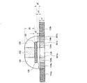
以下に、本実施の形態による半導体装置の作製方法を、図1(A)〜図1(D)、図2(A)〜図2(H)、図6(A)〜図6(B)を用いて説明する。
本実施の形態では、Loff領域のみを有する半導体装置の作製方法を、図3(A)〜図3(D)に示す。また、本実施の形態において、実施の形態1と同じものについては同じ符号を用い、詳細な説明を省略する。
本実施の形態では、実施の形態2とは別の、Loff領域のみを有する半導体装置の作製方法を、図4(A)〜図4(C)及び図5(A)〜図5(D)に示す。また、本実施の形態において、実施の形態1及び実施の形態2と同じものについては同じ符号を用い、詳細な説明を省略する。
本実施の形態では、本発明を用いてCPU(中央演算装置:Central Processing Unit)を作製した例を、図7(A)〜図7(B)、図8、図9、図10(A)〜図10(C)を用いて説明する。本実施の形態において、実施の形態1〜実施の形態3と同じものについては同じ符号を用い、詳細な説明を省略する。
本実施の形態は、本発明のTFTを有する、ICを用いた無線通信が可能な半導体装置を作成する例を、図11、図12、図13、図14、図15を用いて説明する。
20nm+(30nm×1.6)=68nm
112 下地絶縁膜
113 島状半導体膜
114 ゲート絶縁膜
115 導電膜
116 導電膜
117 レジスト
118 導電膜
119 レジスト
120 ゲート電極
121 レジスト
122 ゲート電極
123 レジスト
124a 低濃度不純物領域
124b 低濃度不純物領域
125a 低濃度不純物領域
125b 低濃度不純物領域
126 チャネル形成領域
127 不純物元素
128 サイドウォール
129 ゲート絶縁膜
130 金属膜
131 シリサイド層
132 不純物元素
133a 高濃度不純物領域
133b 高濃度不純物領域
134a 低濃度不純物領域
134b 低濃度不純物領域
135 層間絶縁膜
136 配線
136a 電極または配線
136b 電極または配線
136c 電極または配線
137a 低濃度不純物領域
137b 低濃度不純物領域
150 ゲート電極
152a 低濃度不純物領域
152b 低濃度不純物領域
154a 低濃度不純物領域
154b 低濃度不純物領域
156 チャネル形成領域
158 サイドウォール
159 ゲート絶縁膜
160 ゲート電極
161 ゲート絶縁膜
162 ゲート電極
163 ゲート電極
163a 高濃度不純物領域
163b 高濃度不純物領域
164a 低濃度不純物領域
164a 低濃度不純物領域
165 ゲート絶縁膜
166a 低濃度不純物領域
166b 低濃度不純物領域
167a 高濃度不純物領域
167b 高濃度不純物領域
171 層間絶縁膜
173 導電層
174 導電層
175 薄膜集積回路
181 TFT
182 TFT
183 CMOS回路
360 基板
361 演算回路
362 演算回路用制御回路部
363 命令解析部
364 割り込み制御部
365 タイミング制御部
366 レジスタ
367 レジスタ制御部
368 バスインターフェース
369 ROM
370 基板
371 画素部
372 走査線駆動回路
373 信号線駆動回路
374 CPU
375 コントロール回路
380 ROMインターフェース
381 CLK1
382 CLK2
384 バンプ
385 プラスチック
387 プリント基板
388 ワイヤ
390 基板
391 薄膜トランジスタアレイ
392 電極
393 配線
394 接続端子
395 樹脂
397 プリント基板
398 異方性導電膜
399 FPC
401 TFT
402 TFT
403 TFT
404 TFT
411 メモリセルアレイ
414 出力線
415 列デコーダ
416 行デコーダ
417 制御線
422 高電圧電源
423 低電圧電源
424 ビット線(データ線)
425 ビット線(データ線)
427 配線
428 配線
431 電源線
432 配線
433 電源線
434 配線
441 nチャネル型TFT
442 pチャネル型TFT
511 基板
512 下地絶縁膜
520 ゲート電極
522 ゲート電極
524a 低濃度不純物領域
524b 低濃度不純物領域
526 チャネル形成領域
528 サイドウォール
529 ゲート絶縁膜
531 シリサイド層
533a 高濃度不純物領域
533b 高濃度不純物領域
534a 低濃度不純物領域
534b 低濃度不純物領域
535 層間絶縁膜
536 電極または配線
536a 電極または配線
536c 電極または配線
536d 電極または配線
536e 電極または配線
550 ゲート電極
552 ゲート電極
554a 低濃度不純物領域
556 チャネル形成領域
558 サイドウォール
559 ゲート絶縁膜
563a 高濃度不純物領域
563b 高濃度不純物領域
564a 低濃度不純物領域
564b 低濃度不純物領域
571 層間絶縁膜
573 導電層
574 導電層
577 導電層
578 導電層
579 空隙
581 TFT
582 TFT
900 マスクROM
901 信号出力制御回路
902 CRC回路
903 クロック発生回路
904 コード抽出回路
905 コード判定回路
906 整流回路
907 復調回路
908 アナログアンプ
909 変調回路
911 リセット回路
912 保持容量
913 整流回路
914 高周波回路
915 電源回路
917 アンテナ
920 メモリセルアレイ
921 列デコーダ
922 行デコーダ
931 半導体装置
Claims (1)
- 基板上に、島状半導体膜を形成し、
前記島状半導体膜上にゲート絶縁膜を形成し、
前記ゲート絶縁膜上に、第1の導電膜及び第2の導電膜を形成し、
前記第2の導電膜を第1のエッチングをすることにより、第3の導電膜を形成し、
前記第1の導電膜を第2のエッチングをすることにより、第1のゲート電極を形成し、
前記第3の導電膜を第3のエッチングをすることにより、第2のゲート電極を形成し、かつ、前記第1のゲート電極と重なる領域以外の前記ゲート絶縁膜を前記第3のエッチングをすることにより、前記ゲート絶縁膜の膜厚を薄くし、
前記第2のゲート電極をマスクとして、前記第1のゲート電極及び前記ゲート絶縁膜を通過させて前記島状半導体膜に第1の不純物元素を添加することにより、前記島状半導体膜において、
前記第2のゲート電極と重なる領域にチャネル形成領域を形成し、
前記第1のゲート電極と重なる領域に第1の低濃度不純物領域を形成し、
前記第1の不純物元素が前記ゲート絶縁膜のみを通過した前記島状半導体膜の両端の領域に不純物領域を形成し、前記不純物領域の前記第1の不純物元素の濃度は、前記半導体膜の上面から底面に向かって増加し、
前記ゲート絶縁膜、前記第1のゲート電極、及び前記第2のゲート電極を覆って、絶縁層を形成し、
前記絶縁層を第4のエッチングをすることにより、前記第1のゲート電極及び前記第2のゲート電極の側面に、サイドウォールを形成し、
前記サイドウォール、前記第1のゲート電極、及び前記第2のゲート電極をマスクとして、前記島状半導体膜に第2の不純物元素を添加することにより、前記不純物領域において、前記サイドウォールに領域に覆われなかった領域に高濃度不純物領域を形成し、かつ、前記ゲート絶縁膜及び前記サイドウォールに覆われた領域に第2の低濃度不純物領域を形成することを特徴とする半導体装置の作製方法。
Priority Applications (1)
| Application Number | Priority Date | Filing Date | Title |
|---|---|---|---|
| JP2007315322A JP5352081B2 (ja) | 2006-12-20 | 2007-12-06 | 半導体装置の作製方法 |
Applications Claiming Priority (3)
| Application Number | Priority Date | Filing Date | Title |
|---|---|---|---|
| JP2006343412 | 2006-12-20 | ||
| JP2006343412 | 2006-12-20 | ||
| JP2007315322A JP5352081B2 (ja) | 2006-12-20 | 2007-12-06 | 半導体装置の作製方法 |
Publications (3)
| Publication Number | Publication Date |
|---|---|
| JP2008177546A JP2008177546A (ja) | 2008-07-31 |
| JP2008177546A5 JP2008177546A5 (ja) | 2011-01-20 |
| JP5352081B2 true JP5352081B2 (ja) | 2013-11-27 |
Family
ID=39541600
Family Applications (1)
| Application Number | Title | Priority Date | Filing Date |
|---|---|---|---|
| JP2007315322A Expired - Fee Related JP5352081B2 (ja) | 2006-12-20 | 2007-12-06 | 半導体装置の作製方法 |
Country Status (3)
| Country | Link |
|---|---|
| US (1) | US7705358B2 (ja) |
| JP (1) | JP5352081B2 (ja) |
| CN (1) | CN101207156B (ja) |
Families Citing this family (14)
| Publication number | Priority date | Publication date | Assignee | Title |
|---|---|---|---|---|
| TWI426565B (zh) * | 2009-10-15 | 2014-02-11 | Au Optronics Corp | 顯示面板及薄膜電晶體之閘極絕緣層的重工方法 |
| KR101969291B1 (ko) | 2010-02-26 | 2019-04-17 | 가부시키가이샤 한도오따이 에네루기 켄큐쇼 | 반도체 장치 |
| KR20130055607A (ko) | 2010-04-23 | 2013-05-28 | 가부시키가이샤 한도오따이 에네루기 켄큐쇼 | 반도체 장치의 제작 방법 |
| US8796682B2 (en) | 2011-11-11 | 2014-08-05 | Semiconductor Energy Laboratory Co., Ltd. | Method for manufacturing a semiconductor device |
| US8878177B2 (en) | 2011-11-11 | 2014-11-04 | Semiconductor Energy Laboratory Co., Ltd. | Semiconductor device and method for manufacturing semiconductor device |
| US20130137232A1 (en) | 2011-11-30 | 2013-05-30 | Semiconductor Energy Laboratory Co., Ltd. | Method for forming oxide semiconductor film and method for manufacturing semiconductor device |
| CN103137486B (zh) * | 2011-11-30 | 2016-08-03 | 中国科学院微电子研究所 | 半导体器件制造方法 |
| CN103178006B (zh) * | 2013-03-29 | 2015-09-23 | 上海和辉光电有限公司 | 调整低温多晶硅晶体管阀值电压的方法 |
| US9443876B2 (en) | 2014-02-05 | 2016-09-13 | Semiconductor Energy Laboratory Co., Ltd. | Semiconductor device, display device including the semiconductor device, display module including the display device, and electronic device including the semiconductor device, the display device, and the display module |
| US10002971B2 (en) * | 2014-07-03 | 2018-06-19 | Semiconductor Energy Laboratory Co., Ltd. | Semiconductor device and display device including the semiconductor device |
| US9087689B1 (en) | 2014-07-11 | 2015-07-21 | Inoso, Llc | Method of forming a stacked low temperature transistor and related devices |
| CN104409518B (zh) * | 2014-12-11 | 2018-11-09 | 昆山国显光电有限公司 | 薄膜晶体管及其制备方法 |
| JP2017041596A (ja) * | 2015-08-21 | 2017-02-23 | 株式会社Joled | 薄膜トランジスタ、半導体装置および電子機器 |
| KR102448033B1 (ko) * | 2015-12-21 | 2022-09-28 | 삼성디스플레이 주식회사 | 박막 트랜지스터의 제조 방법, 박막 트랜지스터 기판, 및 평판 표시 장치 |
Family Cites Families (84)
| Publication number | Priority date | Publication date | Assignee | Title |
|---|---|---|---|---|
| JP2553704B2 (ja) | 1989-06-16 | 1996-11-13 | 松下電子工業株式会社 | 半導体装置の製造方法 |
| US6008133A (en) | 1991-04-04 | 1999-12-28 | Hitachi, Ltd. | Method and apparatus for dry etching |
| JP2564725B2 (ja) | 1991-12-24 | 1996-12-18 | 株式会社半導体エネルギー研究所 | Mos型トランジスタの作製方法 |
| US5485019A (en) * | 1992-02-05 | 1996-01-16 | Semiconductor Energy Laboratory Co., Ltd. | Semiconductor device and method for forming the same |
| JPH06124962A (ja) | 1992-10-09 | 1994-05-06 | Semiconductor Energy Lab Co Ltd | 薄膜状半導体装置およびその作製方法 |
| TW232751B (en) | 1992-10-09 | 1994-10-21 | Semiconductor Energy Res Co Ltd | Semiconductor device and method for forming the same |
| US5576556A (en) | 1993-08-20 | 1996-11-19 | Semiconductor Energy Laboratory Co., Ltd. | Thin film semiconductor device with gate metal oxide and sidewall spacer |
| US6624477B1 (en) | 1992-10-09 | 2003-09-23 | Semiconductor Energy Laboratory Co., Ltd. | Semiconductor device and method for manufacturing the same |
| TW226478B (en) | 1992-12-04 | 1994-07-11 | Semiconductor Energy Res Co Ltd | Semiconductor device and method for manufacturing the same |
| JP3437863B2 (ja) * | 1993-01-18 | 2003-08-18 | 株式会社半導体エネルギー研究所 | Mis型半導体装置の作製方法 |
| EP0612102B1 (en) | 1993-02-15 | 2001-09-26 | Semiconductor Energy Laboratory Co., Ltd. | Process for the fabrication of a crystallised semiconductor layer |
| JP3107941B2 (ja) | 1993-03-05 | 2000-11-13 | 株式会社半導体エネルギー研究所 | 薄膜トランジスタおよびその作製方法 |
| JP3193803B2 (ja) | 1993-03-12 | 2001-07-30 | 株式会社半導体エネルギー研究所 | 半導体素子の作製方法 |
| KR100203982B1 (ko) | 1993-03-12 | 1999-06-15 | 야마자끼 순페이 | 반도체장치 및 그의 제작방법 |
| TW297142B (ja) | 1993-09-20 | 1997-02-01 | Handotai Energy Kenkyusho Kk | |
| TW299897U (en) | 1993-11-05 | 1997-03-01 | Semiconductor Energy Lab | A semiconductor integrated circuit |
| JP3253808B2 (ja) | 1994-07-07 | 2002-02-04 | 株式会社半導体エネルギー研究所 | 半導体装置およびその作製方法 |
| JP3464287B2 (ja) | 1994-09-05 | 2003-11-05 | 株式会社半導体エネルギー研究所 | 半導体装置の作製方法 |
| JP4083821B2 (ja) | 1994-09-15 | 2008-04-30 | 株式会社半導体エネルギー研究所 | 半導体装置の作製方法 |
| US6670640B1 (en) | 1994-09-15 | 2003-12-30 | Semiconductor Energy Laboratory Co., Ltd. | Method for producing semiconductor device |
| JP3173760B2 (ja) | 1994-11-11 | 2001-06-04 | 株式会社半導体エネルギー研究所 | 半導体装置の作製方法 |
| JP4130237B2 (ja) | 1995-01-28 | 2008-08-06 | 株式会社半導体エネルギー研究所 | 結晶性珪素膜の作製方法及び半導体装置の作製方法 |
| JPH08250739A (ja) | 1995-03-13 | 1996-09-27 | Nec Corp | 半導体装置の製造方法 |
| JPH08264798A (ja) | 1995-03-23 | 1996-10-11 | Semiconductor Energy Lab Co Ltd | 半導体装置および半導体装置作製方法 |
| JP3329128B2 (ja) | 1995-03-28 | 2002-09-30 | ソニー株式会社 | 半導体装置の製造方法 |
| JPH10135475A (ja) | 1996-10-31 | 1998-05-22 | Semiconductor Energy Lab Co Ltd | 半導体装置およびその作製方法 |
| JP3942683B2 (ja) | 1997-02-12 | 2007-07-11 | 株式会社半導体エネルギー研究所 | 半導体装置作製方法 |
| US5994985A (en) * | 1997-12-05 | 1999-11-30 | Rockwell Science Center, Llc | Integrable high-Q tunable capacitor and method |
| JP3129232B2 (ja) | 1997-05-08 | 2001-01-29 | 日本電気株式会社 | 半導体装置の製造方法 |
| JP4175437B2 (ja) | 1997-09-16 | 2008-11-05 | 株式会社半導体エネルギー研究所 | 半導体装置およびその作製方法 |
| US6369410B1 (en) | 1997-12-15 | 2002-04-09 | Semiconductor Energy Laboratory Co., Ltd. | Semiconductor device and method of manufacturing the semiconductor device |
| US6048791A (en) | 1998-03-31 | 2000-04-11 | Kabushiki Kaisha Toshiba | Semiconductor device with electrode formed of conductive layer consisting of polysilicon layer and metal-silicide layer and its manufacturing method |
| US6274887B1 (en) | 1998-11-02 | 2001-08-14 | Semiconductor Energy Laboratory Co., Ltd. | Semiconductor device and manufacturing method therefor |
| US7141821B1 (en) * | 1998-11-10 | 2006-11-28 | Semiconductor Energy Laboratory Co., Ltd. | Semiconductor device having an impurity gradient in the impurity regions and method of manufacture |
| US6365917B1 (en) | 1998-11-25 | 2002-04-02 | Semiconductor Energy Laboratory Co., Ltd. | Semiconductor device |
| JP2000174282A (ja) | 1998-12-03 | 2000-06-23 | Semiconductor Energy Lab Co Ltd | 半導体装置 |
| US6259138B1 (en) | 1998-12-18 | 2001-07-10 | Semiconductor Energy Laboratory Co., Ltd. | Semiconductor device having multilayered gate electrode and impurity regions overlapping therewith |
| US6545359B1 (en) | 1998-12-18 | 2003-04-08 | Semiconductor Energy Laboratory Co., Ltd. | Wiring line and manufacture process thereof, and semiconductor device and manufacturing process thereof |
| US6531713B1 (en) | 1999-03-19 | 2003-03-11 | Semiconductor Energy Laboratory Co., Ltd. | Electro-optical device and manufacturing method thereof |
| JP2001118927A (ja) | 1999-10-22 | 2001-04-27 | Mitsubishi Electric Corp | 半導体装置およびその製造方法 |
| US6646287B1 (en) | 1999-11-19 | 2003-11-11 | Semiconductor Energy Laboratory Co., Ltd. | Semiconductor device with tapered gate and insulating film |
| TW473800B (en) | 1999-12-28 | 2002-01-21 | Semiconductor Energy Lab | Method of manufacturing a semiconductor device |
| US6825488B2 (en) | 2000-01-26 | 2004-11-30 | Semiconductor Energy Laboratory Co., Ltd. | Semiconductor device and manufacturing method thereof |
| US6646692B2 (en) | 2000-01-26 | 2003-11-11 | Semiconductor Energy Laboratory Co., Ltd. | Liquid-crystal display device and method of fabricating the same |
| US6391788B1 (en) | 2000-02-25 | 2002-05-21 | Applied Materials, Inc. | Two etchant etch method |
| TW495854B (en) | 2000-03-06 | 2002-07-21 | Semiconductor Energy Lab | Semiconductor device and manufacturing method thereof |
| US6690437B2 (en) | 2000-04-18 | 2004-02-10 | Semiconductor Energy Laboratory Co., Ltd. | Electro-optical device |
| US6706544B2 (en) | 2000-04-19 | 2004-03-16 | Semiconductor Energy Laboratory Co., Ltd. | Light emitting device and fabricating method thereof |
| US6847341B2 (en) | 2000-04-19 | 2005-01-25 | Semiconductor Energy Laboratory Co., Ltd. | Electronic device and method of driving the same |
| US6611108B2 (en) | 2000-04-26 | 2003-08-26 | Semiconductor Energy Laboratory Co., Ltd. | Electronic device and driving method thereof |
| US6747289B2 (en) | 2000-04-27 | 2004-06-08 | Semiconductor Energy Laboratory Co., Ltd. | Semiconductor device and method of fabricating thereof |
| US6794229B2 (en) | 2000-04-28 | 2004-09-21 | Semiconductor Energy Laboratory Co., Ltd. | Manufacturing method for semiconductor device |
| TW480576B (en) | 2000-05-12 | 2002-03-21 | Semiconductor Energy Lab | Semiconductor device and method for manufacturing same |
| TWI224806B (en) | 2000-05-12 | 2004-12-01 | Semiconductor Energy Lab | Semiconductor device and manufacturing method thereof |
| TW501282B (en) | 2000-06-07 | 2002-09-01 | Semiconductor Energy Lab | Method of manufacturing semiconductor device |
| US7223643B2 (en) | 2000-08-11 | 2007-05-29 | Semiconductor Energy Laboratory Co., Ltd. | Method of manufacturing a semiconductor device |
| US6777275B1 (en) | 2000-11-15 | 2004-08-17 | Advanced Micro Devices, Inc. | Single anneal for dopant activation and silicide formation |
| JP4954366B2 (ja) | 2000-11-28 | 2012-06-13 | 株式会社半導体エネルギー研究所 | 半導体装置の作製方法 |
| US6858480B2 (en) | 2001-01-18 | 2005-02-22 | Semiconductor Energy Laboratory Co., Ltd. | Method of manufacturing semiconductor device |
| JP4926329B2 (ja) | 2001-03-27 | 2012-05-09 | 株式会社半導体エネルギー研究所 | 半導体装置およびその作製方法、電気器具 |
| TW546846B (en) * | 2001-05-30 | 2003-08-11 | Matsushita Electric Ind Co Ltd | Thin film transistor and method for manufacturing the same |
| US6608361B2 (en) * | 2001-07-31 | 2003-08-19 | G-Plus, Inc. | On-chip inductor using active magnetic energy recovery |
| US6773944B2 (en) | 2001-11-07 | 2004-08-10 | Semiconductor Energy Laboratory Co., Ltd. | Method of manufacturing a semiconductor device |
| CA2417395A1 (en) * | 2002-01-28 | 2003-07-28 | James William Haslett | Monolithic transformer compensated circuit |
| JP4237442B2 (ja) | 2002-03-01 | 2009-03-11 | 株式会社半導体エネルギー研究所 | 半透過型液晶表示装置 |
| US7344825B2 (en) | 2002-04-04 | 2008-03-18 | Semiconductor Energy Laboratory Co., Ltd. | Method of fabricating semiconductor device, and developing apparatus using the method |
| US7875419B2 (en) | 2002-10-29 | 2011-01-25 | Semiconductor Energy Laboratory Co., Ltd. | Method for removing resist pattern and method for manufacturing semiconductor device |
| US7132369B2 (en) | 2002-12-31 | 2006-11-07 | Applied Materials, Inc. | Method of forming a low-K dual damascene interconnect structure |
| JP2004247413A (ja) * | 2003-02-12 | 2004-09-02 | Sharp Corp | トランジスタおよびその製造方法、並びに該トランジスタを用いた液晶表示装置 |
| US7115517B2 (en) | 2003-04-07 | 2006-10-03 | Applied Materials, Inc. | Method of fabricating a dual damascene interconnect structure |
| US6908850B2 (en) | 2003-09-10 | 2005-06-21 | International Business Machines Corporation | Structure and method for silicided metal gate transistors |
| JP4606006B2 (ja) | 2003-09-11 | 2011-01-05 | ルネサスエレクトロニクス株式会社 | 半導体装置の製造方法 |
| US7176522B2 (en) | 2003-11-25 | 2007-02-13 | Taiwan Semiconductor Manufacturing Company, Ltd. | Semiconductor device having high drive current and method of manufacturing thereof |
| US7214568B2 (en) | 2004-02-06 | 2007-05-08 | Agere Systems Inc. | Semiconductor device configured for reducing post-fabrication damage |
| US7374983B2 (en) | 2004-04-08 | 2008-05-20 | Semiconductor Energy Laboratory Co., Ltd. | Semiconductor device and manufacturing method thereof |
| US7288480B2 (en) | 2004-04-23 | 2007-10-30 | Semiconductor Energy Laboratory Co., Ltd. | Thin film integrated circuit and method for manufacturing the same, CPU, memory, electronic card and electronic device |
| JP4519512B2 (ja) | 2004-04-28 | 2010-08-04 | 株式会社半導体エネルギー研究所 | 半導体装置の作製方法、除去方法 |
| JP5238125B2 (ja) * | 2004-11-04 | 2013-07-17 | 株式会社半導体エネルギー研究所 | 半導体装置の作製方法 |
| TWI382455B (zh) | 2004-11-04 | 2013-01-11 | Semiconductor Energy Lab | 半導體裝置和其製造方法 |
| US7575959B2 (en) | 2004-11-26 | 2009-08-18 | Semiconductor Energy Laboratory Co., Ltd. | Manufacturing method of semiconductor device |
| JP5121145B2 (ja) * | 2005-03-07 | 2013-01-16 | 株式会社半導体エネルギー研究所 | 半導体装置の作製方法 |
| US20060197088A1 (en) | 2005-03-07 | 2006-09-07 | Semiconductor Energy Laboratory Co., Ltd. | Semiconductor device and manufacturing method of the same |
| US7410839B2 (en) * | 2005-04-28 | 2008-08-12 | Semiconductor Energy Laboratory Co., Ltd. | Thin film transistor and manufacturing method thereof |
| US7605410B2 (en) * | 2006-02-23 | 2009-10-20 | Semiconductor Energy Laboratory Co., Ltd. | Semiconductor device and manufacturing method thereof |
-
2007
- 2007-12-06 JP JP2007315322A patent/JP5352081B2/ja not_active Expired - Fee Related
- 2007-12-14 US US11/957,270 patent/US7705358B2/en not_active Expired - Fee Related
- 2007-12-20 CN CN2007101599212A patent/CN101207156B/zh not_active Expired - Fee Related
Also Published As
| Publication number | Publication date |
|---|---|
| US20080150027A1 (en) | 2008-06-26 |
| CN101207156A (zh) | 2008-06-25 |
| CN101207156B (zh) | 2011-03-23 |
| JP2008177546A (ja) | 2008-07-31 |
| US7705358B2 (en) | 2010-04-27 |
Similar Documents
| Publication | Publication Date | Title |
|---|---|---|
| JP5352081B2 (ja) | 半導体装置の作製方法 | |
| JP6694993B2 (ja) | 半導体装置およびその作製方法 | |
| US6841434B2 (en) | Method of fabricating semiconductor device | |
| US7692194B2 (en) | Semiconductor device | |
| US7166863B2 (en) | Semiconductor element, semiconductor device, electronic device, TV set and digital camera | |
| JP5526208B2 (ja) | 半導体装置および半導体装置の作製方法 | |
| JPH05114724A (ja) | 絶縁ゲイト型半導体装置およびその作製方法 | |
| US8193574B2 (en) | Non-volatile semiconductor memory device | |
| JPH10209465A (ja) | 半導体装置およびその作製方法 | |
| JP4141292B2 (ja) | 半導体装置 | |
| JP5121207B2 (ja) | 半導体装置及びその作製方法 | |
| JP3501977B2 (ja) | 半導体装置 | |
| JP4421564B2 (ja) | 半導体装置の作製方法 | |
| JP4141307B2 (ja) | 半導体装置の作製方法 | |
| JP4526773B2 (ja) | 半導体装置の作製方法 | |
| JP3380546B2 (ja) | 半導体装置 | |
| JP3494280B2 (ja) | 絶縁ゲイト型電界効果半導体装置 | |
| JP2008166749A (ja) | 薄膜トランジスタ及びその作製方法、並びに該薄膜トランジスタを有する半導体装置 | |
| JP4338996B2 (ja) | 半導体装置の作製方法 | |
| JP2009004587A (ja) | 半導体装置及び当該半導体装置を具備する電子機器 | |
| JP2000031498A (ja) | 半導体装置 | |
| JPH114006A (ja) | 絶縁ゲイト型電界効果半導体装置の作製方法 |
Legal Events
| Date | Code | Title | Description |
|---|---|---|---|
| A521 | Request for written amendment filed |
Free format text: JAPANESE INTERMEDIATE CODE: A523 Effective date: 20101201 |
|
| A621 | Written request for application examination |
Free format text: JAPANESE INTERMEDIATE CODE: A621 Effective date: 20101201 |
|
| A977 | Report on retrieval |
Free format text: JAPANESE INTERMEDIATE CODE: A971007 Effective date: 20121211 |
|
| A131 | Notification of reasons for refusal |
Free format text: JAPANESE INTERMEDIATE CODE: A131 Effective date: 20121225 |
|
| TRDD | Decision of grant or rejection written | ||
| A01 | Written decision to grant a patent or to grant a registration (utility model) |
Free format text: JAPANESE INTERMEDIATE CODE: A01 Effective date: 20130820 |
|
| A61 | First payment of annual fees (during grant procedure) |
Free format text: JAPANESE INTERMEDIATE CODE: A61 Effective date: 20130826 |
|
| R150 | Certificate of patent or registration of utility model |
Ref document number: 5352081 Country of ref document: JP Free format text: JAPANESE INTERMEDIATE CODE: R150 Free format text: JAPANESE INTERMEDIATE CODE: R150 |
|
| R250 | Receipt of annual fees |
Free format text: JAPANESE INTERMEDIATE CODE: R250 |
|
| R250 | Receipt of annual fees |
Free format text: JAPANESE INTERMEDIATE CODE: R250 |
|
| R250 | Receipt of annual fees |
Free format text: JAPANESE INTERMEDIATE CODE: R250 |
|
| LAPS | Cancellation because of no payment of annual fees |