JP5259552B2 - 不揮発性半導体記憶装置及びその駆動方法 - Google Patents
不揮発性半導体記憶装置及びその駆動方法 Download PDFInfo
- Publication number
- JP5259552B2 JP5259552B2 JP2009251891A JP2009251891A JP5259552B2 JP 5259552 B2 JP5259552 B2 JP 5259552B2 JP 2009251891 A JP2009251891 A JP 2009251891A JP 2009251891 A JP2009251891 A JP 2009251891A JP 5259552 B2 JP5259552 B2 JP 5259552B2
- Authority
- JP
- Japan
- Prior art keywords
- potential
- film
- hole
- gate electrode
- control gate
- Prior art date
- Legal status (The legal status is an assumption and is not a legal conclusion. Google has not performed a legal analysis and makes no representation as to the accuracy of the status listed.)
- Active
Links
Images


Classifications
-
- H—ELECTRICITY
- H10—SEMICONDUCTOR DEVICES; ELECTRIC SOLID-STATE DEVICES NOT OTHERWISE PROVIDED FOR
- H10B—ELECTRONIC MEMORY DEVICES
- H10B41/00—Electrically erasable-and-programmable ROM [EEPROM] devices comprising floating gates
- H10B41/20—Electrically erasable-and-programmable ROM [EEPROM] devices comprising floating gates characterised by three-dimensional [3D] arrangements, e.g. with cells on different height levels
-
- G—PHYSICS
- G11—INFORMATION STORAGE
- G11C—STATIC STORES
- G11C16/00—Erasable programmable read-only memories
- G11C16/02—Erasable programmable read-only memories electrically programmable
- G11C16/04—Erasable programmable read-only memories electrically programmable using variable threshold transistors, e.g. FAMOS
- G11C16/0466—Erasable programmable read-only memories electrically programmable using variable threshold transistors, e.g. FAMOS comprising cells with charge storage in an insulating layer, e.g. metal-nitride-oxide-silicon [MNOS], silicon-oxide-nitride-oxide-silicon [SONOS]
-
- G—PHYSICS
- G11—INFORMATION STORAGE
- G11C—STATIC STORES
- G11C16/00—Erasable programmable read-only memories
- G11C16/02—Erasable programmable read-only memories electrically programmable
- G11C16/06—Auxiliary circuits, e.g. for writing into memory
-
- G—PHYSICS
- G11—INFORMATION STORAGE
- G11C—STATIC STORES
- G11C16/00—Erasable programmable read-only memories
- G11C16/02—Erasable programmable read-only memories electrically programmable
- G11C16/06—Auxiliary circuits, e.g. for writing into memory
- G11C16/34—Determination of programming status, e.g. threshold voltage, overprogramming or underprogramming, retention
-
- H—ELECTRICITY
- H10—SEMICONDUCTOR DEVICES; ELECTRIC SOLID-STATE DEVICES NOT OTHERWISE PROVIDED FOR
- H10B—ELECTRONIC MEMORY DEVICES
- H10B43/00—EEPROM devices comprising charge-trapping gate insulators
- H10B43/10—EEPROM devices comprising charge-trapping gate insulators characterised by the top-view layout
-
- H—ELECTRICITY
- H10—SEMICONDUCTOR DEVICES; ELECTRIC SOLID-STATE DEVICES NOT OTHERWISE PROVIDED FOR
- H10B—ELECTRONIC MEMORY DEVICES
- H10B43/00—EEPROM devices comprising charge-trapping gate insulators
- H10B43/20—EEPROM devices comprising charge-trapping gate insulators characterised by three-dimensional [3D] arrangements, e.g. with cells on different height levels
- H10B43/23—EEPROM devices comprising charge-trapping gate insulators characterised by three-dimensional [3D] arrangements, e.g. with cells on different height levels with source and drain on different levels, e.g. with sloping channels
- H10B43/27—EEPROM devices comprising charge-trapping gate insulators characterised by three-dimensional [3D] arrangements, e.g. with cells on different height levels with source and drain on different levels, e.g. with sloping channels the channels comprising vertical portions, e.g. U-shaped channels
-
- H—ELECTRICITY
- H10—SEMICONDUCTOR DEVICES; ELECTRIC SOLID-STATE DEVICES NOT OTHERWISE PROVIDED FOR
- H10D—INORGANIC ELECTRIC SEMICONDUCTOR DEVICES
- H10D84/00—Integrated devices formed in or on semiconductor substrates that comprise only semiconducting layers, e.g. on Si wafers or on GaAs-on-Si wafers
- H10D84/01—Manufacture or treatment
- H10D84/0123—Integrating together multiple components covered by H10D12/00 or H10D30/00, e.g. integrating multiple IGBTs
- H10D84/0126—Integrating together multiple components covered by H10D12/00 or H10D30/00, e.g. integrating multiple IGBTs the components including insulated gates, e.g. IGFETs
- H10D84/0149—Manufacturing their interconnections or electrodes, e.g. source or drain electrodes
-
- H—ELECTRICITY
- H10—SEMICONDUCTOR DEVICES; ELECTRIC SOLID-STATE DEVICES NOT OTHERWISE PROVIDED FOR
- H10D—INORGANIC ELECTRIC SEMICONDUCTOR DEVICES
- H10D84/00—Integrated devices formed in or on semiconductor substrates that comprise only semiconducting layers, e.g. on Si wafers or on GaAs-on-Si wafers
- H10D84/01—Manufacture or treatment
- H10D84/0123—Integrating together multiple components covered by H10D12/00 or H10D30/00, e.g. integrating multiple IGBTs
- H10D84/0126—Integrating together multiple components covered by H10D12/00 or H10D30/00, e.g. integrating multiple IGBTs the components including insulated gates, e.g. IGFETs
- H10D84/016—Integrating together multiple components covered by H10D12/00 or H10D30/00, e.g. integrating multiple IGBTs the components including insulated gates, e.g. IGFETs the components including vertical IGFETs
-
- H—ELECTRICITY
- H10—SEMICONDUCTOR DEVICES; ELECTRIC SOLID-STATE DEVICES NOT OTHERWISE PROVIDED FOR
- H10P—GENERIC PROCESSES OR APPARATUS FOR THE MANUFACTURE OR TREATMENT OF DEVICES COVERED BY CLASS H10
- H10P50/00—Etching of wafers, substrates or parts of devices
- H10P50/20—Dry etching; Plasma etching; Reactive-ion etching
- H10P50/24—Dry etching; Plasma etching; Reactive-ion etching of semiconductor materials
- H10P50/242—Dry etching; Plasma etching; Reactive-ion etching of semiconductor materials of Group IV materials
Landscapes
- Engineering & Computer Science (AREA)
- Microelectronics & Electronic Packaging (AREA)
- Semiconductor Memories (AREA)
- Non-Volatile Memory (AREA)
- Read Only Memory (AREA)
Description
先ず、本発明の第1の実施形態について説明する。
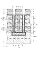
図1は、本実施形態に係る不揮発性半導体記憶装置の特徴を模式的に例示する図であり、
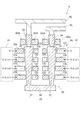
図2は、本実施形態に係る不揮発性半導体記憶装置を例示する斜視図であり、
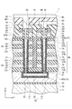
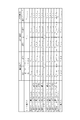
図3は、本実施形態に係る不揮発性半導体記憶装置を例示する断面図であり、
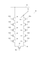
図4は、本実施形態に係る不揮発性半導体記憶装置のメモリストリングを例示する回路図であり、
図5は、本実施形態に係る不揮発性半導体記憶装置の電極膜を例示する平面図であり、
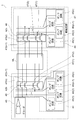
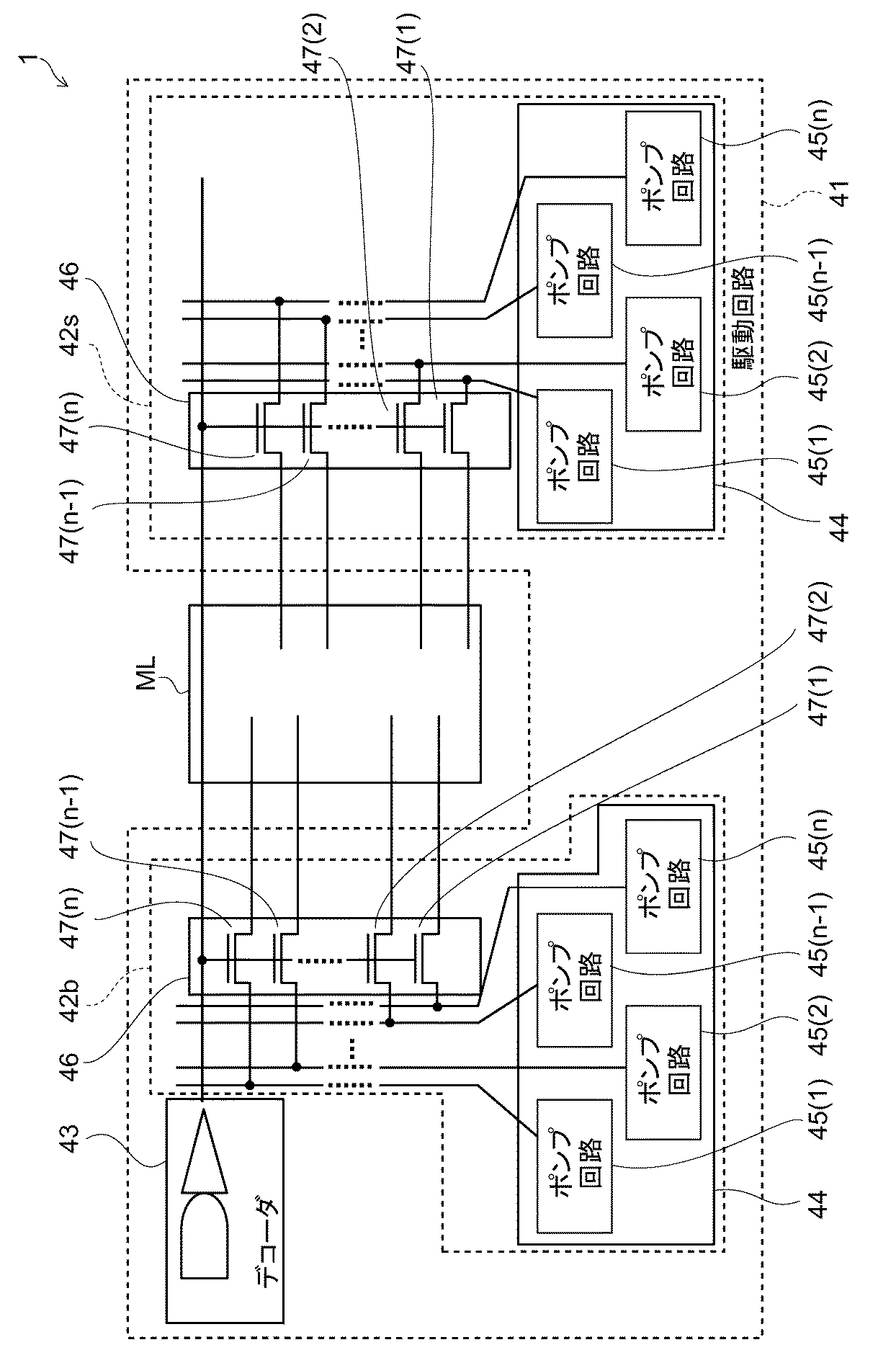
図6は、本実施形態に係る不揮発性半導体記憶装置の駆動回路を例示する回路図である。
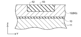
なお、図1及び図2においては、図を見やすくするために、導電部分のみを図示し、絶縁部分は図示を省略している。後述する図10についても同様である。また、図2においては、図示の便宜上、シリコンピラーはZ方向の位置に拘わらず同じ太さで描かれている。
図1に示すように、本実施形態に係る不揮発性半導体記憶装置1の特徴は、シリコンピラー31と制御ゲート電極CGとの交差部分にメモリトランジスタが設けられた一括加工型の3次元積層型記憶装置において、制御ゲート電極CGに駆動電位を供給する駆動回路41が、貫通している貫通ホールの径が小さい制御ゲート電極CGほど、シリコンピラー31との間の電位差が小さくなるような駆動電位を印加することである。より具体的には、不揮発性半導体記憶装置1においては、下段に配置された制御ゲート電極CGほど、シリコンピラー31が埋設される貫通ホールの径が小さくなっているため、駆動回路41は、下段に配置された制御ゲート電極CGに対してほど、低い駆動電位を印加する。
図2及び図3に示すように、本実施形態に係る不揮発性半導体記憶装置1(以下、単に「装置1」ともいう)においては、シリコン基板11が設けられている。シリコン基板11には、メモリセルが形成されるメモリセル領域と、駆動回路が形成される周辺回路領域(図示せず)とが設定されている。周辺回路領域は、メモリセル形成領域の周囲に配置されている。
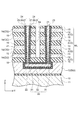
メモリセル領域の特徴は、メモリセルが3次元的に配列された積層体MLが設けられており、積層体MLを貫く貫通ホール21の直径が、下方に行くほど細くなっていることである。以下、メモリセル領域の構成を詳細に説明する。
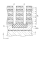
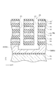
図5に示すように、メモリセル形成領域において設定された複数のブロック50は、Y方向に沿って配列されている。そして、装置1に設けられた導電部材のうち、X方向に延びる導電部材、すなわち、制御ゲート電極CG及び選択ゲート電極SGと、Z方向に延びるU字ピラー30は、ブロック50毎に組分けされている。また、XY平面に沿って形成されているバックゲートBGは、ブロック50毎に分割されており、相互に電気的に分離されている。一方、Y方向に延びるビット線BLは、全てのブロック50を通過するように延びており、全てのブロック50で共有されている。更にまた、シリコン基板11におけるブロック50間の領域には、素子分離膜(図示せず)が形成されている。
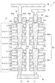
図6に示すように、周辺回路領域においては、メモリストリング38を駆動する駆動回路41が設けられている。駆動回路41においては、積層体MLに形成された各段の制御ゲート電極CGb及び選択ゲート電極SGbに対して駆動電位を印加する電位供給部42bと、各段の制御ゲート電極CGs及び選択ゲート電極SGsに対して駆動電位を印加する電位供給部42sと、制御信号を出力するデコーダ43とが設けられている。
図7は、本実施形態に係る不揮発性半導体記憶装置の動作において、各電極及び配線に印加する電位を例示する図であり、
図8は、本実施形態に係る不揮発性半導体記憶装置の動作において、各段の制御ゲート電極に印加する電位を例示する図であり、
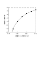
図9は、横軸に貫通ホールの直径をとり、縦軸に制御ゲート電極とシリコンピラーとの間の電圧差をとって、印加電位の決定方法を例示するグラフ図である。
先ず、各メモリトランジスタ35に任意のデータを書き込む書込動作について説明する。データの書込は、1ブロックずつ順番に、X方向に配列された複数個の選択セルに対して同時に行う。図2に示すように、これらの複数個の選択セルは、相互に異なるメモリストリング38に属しているが、同一の制御ゲート電極CGを共有している。また、これらの選択セルが属する複数本のメモリストリング38は、相互に異なるビット線BLに接続されているが、共通の選択ゲート電極SGを貫いており、共通のソース線SLに接続されている。
次に、任意のメモリトランジスタ35に書き込まれたデータを読み出す読出動作について説明する。図7に示すように、駆動回路41が、バックゲートBGにオン電位Vonを印加して、バックゲートトランジスタ37をオン状態とする。また、駆動回路41は、選択ストリングの選択ゲート電極SGs及びSGbにオン電位Von(例えば、3.0V)を印加して、選択トランジスタ36をオン状態とする。一方、駆動回路41は、非選択のメモリストリング38の選択ゲート電極SGs及びSGbにはオフ電位Voff(例えば、0V)を印加して、選択トランジスタ36をオフ状態とする。
次に、メモリトランジスタに書き込まれたデータを消去する消去動作について説明する。データの消去はブロック単位で行う。図7に示すように、駆動回路41は、バックゲートBGにオン電位Vonを印加して、バックゲートトランジスタ37をオン状態とする。また、消去対象となるブロック(以下、「選択ブロック」ともいう)の全ての制御ゲート電極CGに基準電位Vss(例えば、0V)を印加する。更に、ビット線BL及びソース線SLの電位を消去電位Verase(例えば、15V)に昇圧する。更にまた、選択ゲート電極SGb及びSGsに消去電位Veraseよりも低い選択ゲート電位Vsgを印加する。すなわち、Vsg<Veraseとする。
本実施形態によれば、上述の如く、駆動回路41に複数のポンプ回路45が設けられており、各ポンプ回路45が各スイッチ素子47を介して各段の制御ゲート電極CGに接続されていることにより、各段の制御ゲート電極CGに対して、相互に異なる駆動電位を印加することができる。これにより、下方に位置し、貫通ホール21の直径が小さいメモリトランジスタほど、制御ゲート電極CGとシリコンピラー31との間の電位差を小さくすることができ、各メモリトランジスタのONO膜24に印加される電界強度を均一化することができる。この結果、メモリトランジスタの誤動作を防止することができる。この技術は、書込動作、読出動作及び消去動作のうち少なくとも1つの動作において、その動作でシリコンピラーとの間の電位差が最も高くなるような電位を制御ゲート電極に対して供給する際に適用すれば、大きな効果を得ることができる。
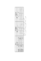
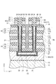
図10は、本実施形態に係る不揮発性半導体記憶装置の特徴を模式的に例示する図である。
図10に示すように、本実施形態においては、貫通ホールが2段構成になっており、各段において、下方に行くほど細くなっている。すなわち、積層体MLは、Z方向に配列された2つの部分積層体ML1及びML2からなり、部分積層体ML1上に部分積層体ML2が積み重ねられている。部分積層体ML1及びML2においては、それぞれ複数枚の絶縁膜15及び電極膜14が積層されている。また、貫通ホール21のうち、部分積層体ML1内に形成された下部21aと、部分積層体ML2内に形成された上部21bは、それぞれ、下方に行くほど細いテーパー状になっている。このため、下部21aの上端部は上部21bの下端部よりも太くなっており、貫通ホール21の内面における下部21aと上部21bとの境界部分には段差が形成されている。
本実施形態は、前述の第1の実施形態に係る不揮発性半導体記憶装置1の製造方法の実施形態である。
図11乃至図19は、本実施形態に係る不揮発性半導体記憶装置の製造方法を例示する工程断面図である。
なお、図11乃至図19は、図3と同じ断面を示している。
Claims (5)
- 基板と、
前記基板上に設けられ、それぞれ複数の絶縁膜及び電極膜が交互に積層され、積層方向に延びる貫通ホールが形成された積層体と、
前記貫通ホールの内部に埋設された半導体ピラーと、
前記電極膜と前記半導体ピラーとの間に設けられた電荷蓄積膜と、
前記電極膜に対して電位を供給する駆動回路と、
を備え、
前記貫通ホールの径は、前記積層方向における位置によって異なっており、
前記駆動回路は、貫通している前記貫通ホールの径が小さい前記電極膜ほど、前記半導体ピラーとの間の電位差が小さくなるような電位を供給することを特徴とする不揮発性半導体記憶装置。 - 前記貫通ホールの径は前記基板に近いほど小さいことを特徴とする請求項1記載の不揮発性半導体記憶装置。
- 前記積層体は、前記積層方向に配列され、それぞれ複数の前記絶縁膜及び前記電極膜が配置された複数の部分積層体を有し、
各前記部分積層体において、前記貫通ホールの径は前記基板に近いほど小さいことを特徴とする請求項1記載の不揮発性半導体記憶装置。 - 前記積層方向から見て、前記貫通ホールの形状は円形であり、
前記貫通ホールにおける一の前記電極膜を貫通する部分の直径をr(μm)とし、前記半導体ピラーと前記一の電極膜との間の電位差であって、前記直径が0.06μmであるときの電位差を1とした場合の相対電位差をVとするとき、前記駆動回路が前記一の電極膜に対して供給する電位は、下記数式に従って決定されていることを特徴とする請求項1〜3のいずれか1つに記載の不揮発性半導体記憶装置。
- 基板、前記基板上に設けられそれぞれ複数の絶縁膜及び電極膜が交互に積層され積層方向に延びる貫通ホールが形成された積層体、前記貫通ホールの内部に埋設された半導体ピラー、及び前記電極膜と前記半導体ピラーとの間に設けられた電荷蓄積膜を含み、前記貫通ホールの径が前記積層方向における位置によって異なっている不揮発性半導体記憶装置の駆動方法であって、
前記電極膜に対して電位を印加する際に、貫通している前記貫通ホールの径が小さい前記電極膜ほど、前記半導体ピラーとの間の電位差が小さくなるような電位を供給することを特徴とする不揮発性半導体記憶装置の駆動方法。
Priority Applications (8)
| Application Number | Priority Date | Filing Date | Title |
|---|---|---|---|
| JP2009251891A JP5259552B2 (ja) | 2009-11-02 | 2009-11-02 | 不揮発性半導体記憶装置及びその駆動方法 |
| US12/851,054 US8218358B2 (en) | 2009-11-02 | 2010-08-05 | Nonvolatile semiconductor memory device and method for driving same |
| KR1020100084677A KR101082228B1 (ko) | 2009-11-02 | 2010-08-31 | 불휘발성 반도체 기억 장치 및 그 구동 방법 |
| US14/327,359 USRE45840E1 (en) | 2009-11-02 | 2014-07-09 | Nonvolatile semiconductor memory device and method for driving same |
| US14/992,650 USRE46785E1 (en) | 2009-11-02 | 2016-01-11 | Nonvolatile semiconductor memory device and method for driving same |
| US15/890,143 USRE48191E1 (en) | 2009-11-02 | 2018-02-06 | Nonvolatile semiconductor memory device and method for driving same |
| US16/926,273 USRE49152E1 (en) | 2009-11-02 | 2020-07-10 | Nonvolatile semiconductor memory device and method for driving same |
| US17/850,399 USRE50330E1 (en) | 2009-11-02 | 2022-06-27 | Nonvolatile semiconductor memory device and method for driving same |
Applications Claiming Priority (1)
| Application Number | Priority Date | Filing Date | Title |
|---|---|---|---|
| JP2009251891A JP5259552B2 (ja) | 2009-11-02 | 2009-11-02 | 不揮発性半導体記憶装置及びその駆動方法 |
Publications (2)
| Publication Number | Publication Date |
|---|---|
| JP2011096340A JP2011096340A (ja) | 2011-05-12 |
| JP5259552B2 true JP5259552B2 (ja) | 2013-08-07 |
Family
ID=43925293
Family Applications (1)
| Application Number | Title | Priority Date | Filing Date |
|---|---|---|---|
| JP2009251891A Active JP5259552B2 (ja) | 2009-11-02 | 2009-11-02 | 不揮発性半導体記憶装置及びその駆動方法 |
Country Status (3)
| Country | Link |
|---|---|
| US (6) | US8218358B2 (ja) |
| JP (1) | JP5259552B2 (ja) |
| KR (1) | KR101082228B1 (ja) |
Cited By (1)
| Publication number | Priority date | Publication date | Assignee | Title |
|---|---|---|---|---|
| KR20120131653A (ko) * | 2011-05-26 | 2012-12-05 | 에스케이하이닉스 주식회사 | 비휘발성 메모리 장치 및 그 제조 방법 |
Families Citing this family (41)
| Publication number | Priority date | Publication date | Assignee | Title |
|---|---|---|---|---|
| JP5086959B2 (ja) * | 2008-09-26 | 2012-11-28 | 株式会社東芝 | 不揮発性半導体記憶装置 |
| JP5380190B2 (ja) * | 2009-07-21 | 2014-01-08 | 株式会社東芝 | 不揮発性半導体記憶装置及びその製造方法 |
| JP5052575B2 (ja) * | 2009-09-01 | 2012-10-17 | 株式会社東芝 | 不揮発性半導体記憶装置 |
| JP4913188B2 (ja) * | 2009-09-18 | 2012-04-11 | 株式会社東芝 | 不揮発性半導体記憶装置 |
| JP2012059830A (ja) * | 2010-09-07 | 2012-03-22 | Toshiba Corp | 半導体記憶装置 |
| KR101198253B1 (ko) | 2010-12-30 | 2012-11-07 | 에스케이하이닉스 주식회사 | 비휘발성 메모리 장치 및 그 제조 방법 |
| US8750040B2 (en) | 2011-01-21 | 2014-06-10 | Micron Technology, Inc. | Memory devices having source lines directly coupled to body regions and methods |
| US8431961B2 (en) * | 2011-02-03 | 2013-04-30 | Micron Technology, Inc. | Memory devices with a connecting region having a band gap lower than a band gap of a body region |
| JP2012203969A (ja) * | 2011-03-25 | 2012-10-22 | Toshiba Corp | 不揮発性半導体記憶装置 |
| JP2013065636A (ja) * | 2011-09-15 | 2013-04-11 | Toshiba Corp | 不揮発性半導体記憶装置およびその製造方法 |
| US9171625B2 (en) | 2012-06-15 | 2015-10-27 | Micron Technology, Inc. | Apparatuses and methods to modify pillar potential |
| JP2014013634A (ja) * | 2012-07-03 | 2014-01-23 | Toshiba Corp | 不揮発性半導体記憶装置及びその動作方法 |
| US8754459B2 (en) | 2012-08-31 | 2014-06-17 | Kabushiki Kaisha Toshiba | Semiconductor memory device |
| US8780632B2 (en) | 2012-11-09 | 2014-07-15 | Sandisk Technologies Inc. | De-duplication techniques using NAND flash based content addressable memory |
| US8780634B2 (en) | 2012-11-09 | 2014-07-15 | Sandisk Technologies Inc. | CAM NAND with OR function and full chip search capability |
| US8634248B1 (en) | 2012-11-09 | 2014-01-21 | Sandisk Technologies Inc. | On-device data analytics using NAND flash based intelligent memory |
| US10127150B2 (en) | 2012-11-09 | 2018-11-13 | Sandisk Technologies Llc | Key value addressed storage drive using NAND flash based content addressable memory |
| US8780633B2 (en) | 2012-11-09 | 2014-07-15 | SanDisk Technologies, Inc. | De-duplication system using NAND flash based content addressable memory |
| US8773909B2 (en) | 2012-11-09 | 2014-07-08 | Sandisk Technologies Inc. | CAM NAND with or function and full chip search capability |
| US8817541B2 (en) | 2012-11-09 | 2014-08-26 | Sandisk Technologies Inc. | Data search using bloom filters and NAND based content addressable memory |
| US8792279B2 (en) | 2012-11-09 | 2014-07-29 | Sandisk Technologies Inc. | Architectures for data analytics using computational NAND memory |
| US8811085B2 (en) | 2012-11-09 | 2014-08-19 | Sandisk Technologies Inc. | On-device data analytics using NAND flash based intelligent memory |
| US8780635B2 (en) | 2012-11-09 | 2014-07-15 | Sandisk Technologies Inc. | Use of bloom filter and improved program algorithm for increased data protection in CAM NAND memory |
| US9075424B2 (en) | 2013-03-06 | 2015-07-07 | Sandisk Technologies Inc. | Compensation scheme to improve the stability of the operational amplifiers |
| JP2014183304A (ja) | 2013-03-19 | 2014-09-29 | Toshiba Corp | 不揮発性半導体記憶装置およびその製造方法 |
| JP2015176620A (ja) * | 2014-03-14 | 2015-10-05 | 株式会社東芝 | 半導体記憶装置 |
| KR102116674B1 (ko) | 2014-03-21 | 2020-06-08 | 삼성전자주식회사 | 비휘발성 메모리 장치 및 그것을 포함하는 저장 장치 및 그것의 동작 방법 |
| WO2015189916A1 (ja) * | 2014-06-10 | 2015-12-17 | ユニサンティス エレクトロニクス シンガポール プライベート リミテッド | 柱状半導体メモリ装置及びその製造方法 |
| US9698342B2 (en) * | 2014-09-11 | 2017-07-04 | Kabushiki Kaisha Toshiba | Contact layer for magnetic tunnel junction element and manufacturing method thereof |
| JP6309909B2 (ja) * | 2015-03-12 | 2018-04-11 | 東芝メモリ株式会社 | 不揮発性半導体記憶装置 |
| JP6290124B2 (ja) | 2015-03-12 | 2018-03-07 | 東芝メモリ株式会社 | 半導体記憶装置 |
| JP2016225614A (ja) | 2015-05-26 | 2016-12-28 | 株式会社半導体エネルギー研究所 | 半導体装置 |
| JP2017107626A (ja) * | 2015-12-10 | 2017-06-15 | 株式会社東芝 | 半導体装置 |
| JP6595357B2 (ja) * | 2016-02-01 | 2019-10-23 | 東芝メモリ株式会社 | メモリデバイス |
| JP2018045752A (ja) | 2016-09-16 | 2018-03-22 | 東芝メモリ株式会社 | 半導体装置 |
| JP2018085160A (ja) | 2016-11-25 | 2018-05-31 | 東芝メモリ株式会社 | 半導体装置およびその動作方法 |
| CN106847821B (zh) | 2017-03-07 | 2018-09-14 | 长江存储科技有限责任公司 | 半导体结构及其形成方法 |
| US10593730B1 (en) * | 2018-10-10 | 2020-03-17 | Micron Technology, Inc. | Three-dimensional memory array |
| KR102723994B1 (ko) | 2019-02-27 | 2024-10-30 | 삼성전자주식회사 | 집적회로 소자 |
| US20200365612A1 (en) * | 2019-05-16 | 2020-11-19 | Macronix International Co., Ltd. | Three dimensional memory device and method for fabricating the same |
| US12581666B2 (en) * | 2023-06-01 | 2026-03-17 | Macronix International Co., Ltd. | Memory device based on thyristors |
Family Cites Families (24)
| Publication number | Priority date | Publication date | Assignee | Title |
|---|---|---|---|---|
| US5798966A (en) * | 1997-03-31 | 1998-08-25 | Intel Corporation | Flash memory VDS compensation techiques to reduce programming variability |
| US6631085B2 (en) * | 2000-04-28 | 2003-10-07 | Matrix Semiconductor, Inc. | Three-dimensional memory array incorporating serial chain diode stack |
| US6903977B2 (en) * | 2001-09-25 | 2005-06-07 | Sony Corporation | Nonvolatile semiconductor memory device and method of producing the same |
| US6925007B2 (en) * | 2001-10-31 | 2005-08-02 | Sandisk Corporation | Multi-state non-volatile integrated circuit memory systems that employ dielectric storage elements |
| JP4647175B2 (ja) * | 2002-04-18 | 2011-03-09 | ルネサスエレクトロニクス株式会社 | 半導体集積回路装置 |
| US7218570B2 (en) * | 2004-12-17 | 2007-05-15 | Sandisk 3D Llc | Apparatus and method for memory operations using address-dependent conditions |
| KR100673170B1 (ko) * | 2005-03-10 | 2007-01-22 | 주식회사 하이닉스반도체 | 향상된 소거 기능을 가지는 플래쉬 메모리 장치 및 그 소거동작 제어 방법 |
| US7671356B2 (en) * | 2005-11-03 | 2010-03-02 | Elpida Memory, Inc. | Electrically rewritable non-volatile memory element and method of manufacturing the same |
| US7545675B2 (en) * | 2005-12-16 | 2009-06-09 | Sandisk Corporation | Reading non-volatile storage with efficient setup |
| US7436703B2 (en) * | 2005-12-27 | 2008-10-14 | Sandisk Corporation | Active boosting to minimize capacitive coupling effect between adjacent gates of flash memory devices |
| JP5016832B2 (ja) * | 2006-03-27 | 2012-09-05 | 株式会社東芝 | 不揮発性半導体記憶装置及びその製造方法 |
| JP4768557B2 (ja) * | 2006-09-15 | 2011-09-07 | 株式会社東芝 | 不揮発性半導体記憶装置及びその製造方法 |
| US7532518B2 (en) * | 2007-06-25 | 2009-05-12 | Spansion Llc | Compensation method to achieve uniform programming speed of flash memory devices |
| JP2009087433A (ja) * | 2007-09-28 | 2009-04-23 | Toshiba Corp | 不揮発性半導体記憶装置 |
| JP5142692B2 (ja) * | 2007-12-11 | 2013-02-13 | 株式会社東芝 | 不揮発性半導体記憶装置 |
| US7961507B2 (en) * | 2008-03-11 | 2011-06-14 | Micron Technology, Inc. | Non-volatile memory with resistive access component |
| KR100991220B1 (ko) * | 2008-07-21 | 2010-11-04 | 삼성전자주식회사 | 접착된 계면을 갖는 기판 내의 콘택 구조체, 이를 구비하는반도체 소자 및 이를 제조하는 방법들 |
| JP5086959B2 (ja) | 2008-09-26 | 2012-11-28 | 株式会社東芝 | 不揮発性半導体記憶装置 |
| JP5388537B2 (ja) * | 2008-10-20 | 2014-01-15 | 株式会社東芝 | 不揮発性半導体記憶装置、及びその製造方法 |
| JP5300419B2 (ja) * | 2008-11-05 | 2013-09-25 | 株式会社東芝 | 不揮発性半導体記憶装置及びその製造方法 |
| JP5364342B2 (ja) * | 2008-11-10 | 2013-12-11 | 株式会社東芝 | 不揮発性半導体記憶装置、及びその製造方法 |
| US9153596B2 (en) * | 2009-02-23 | 2015-10-06 | Cypress Semiconductor Corporation | Adjacent wordline disturb reduction using boron/indium implant |
| JP4913188B2 (ja) * | 2009-09-18 | 2012-04-11 | 株式会社東芝 | 不揮発性半導体記憶装置 |
| US11101266B2 (en) * | 2009-10-12 | 2021-08-24 | Monolithic 3D Inc. | 3D device and devices with bonding |
-
2009
- 2009-11-02 JP JP2009251891A patent/JP5259552B2/ja active Active
-
2010
- 2010-08-05 US US12/851,054 patent/US8218358B2/en not_active Ceased
- 2010-08-31 KR KR1020100084677A patent/KR101082228B1/ko not_active Expired - Fee Related
-
2014
- 2014-07-09 US US14/327,359 patent/USRE45840E1/en active Active
-
2016
- 2016-01-11 US US14/992,650 patent/USRE46785E1/en active Active
-
2018
- 2018-02-06 US US15/890,143 patent/USRE48191E1/en active Active
-
2020
- 2020-07-10 US US16/926,273 patent/USRE49152E1/en active Active
-
2022
- 2022-06-27 US US17/850,399 patent/USRE50330E1/en active Active
Cited By (2)
| Publication number | Priority date | Publication date | Assignee | Title |
|---|---|---|---|---|
| KR20120131653A (ko) * | 2011-05-26 | 2012-12-05 | 에스케이하이닉스 주식회사 | 비휘발성 메모리 장치 및 그 제조 방법 |
| KR101868799B1 (ko) | 2011-05-26 | 2018-06-21 | 에스케이하이닉스 주식회사 | 비휘발성 메모리 장치 및 그 제조 방법 |
Also Published As
| Publication number | Publication date |
|---|---|
| USRE46785E1 (en) | 2018-04-10 |
| USRE45840E1 (en) | 2016-01-12 |
| JP2011096340A (ja) | 2011-05-12 |
| KR101082228B1 (ko) | 2011-11-09 |
| US20110103153A1 (en) | 2011-05-05 |
| KR20110048452A (ko) | 2011-05-11 |
| USRE49152E1 (en) | 2022-07-26 |
| USRE50330E1 (en) | 2025-03-04 |
| USRE48191E1 (en) | 2020-09-01 |
| US8218358B2 (en) | 2012-07-10 |
Similar Documents
| Publication | Publication Date | Title |
|---|---|---|
| JP5259552B2 (ja) | 不揮発性半導体記憶装置及びその駆動方法 | |
| JP5383241B2 (ja) | 不揮発性半導体記憶装置及びその製造方法 | |
| JP5297342B2 (ja) | 不揮発性半導体記憶装置 | |
| JP5112201B2 (ja) | 不揮発性半導体記憶装置 | |
| KR101076125B1 (ko) | 불휘발성 반도체 기억 장치 | |
| JP5388600B2 (ja) | 不揮発性半導体記憶装置の製造方法 | |
| KR101267130B1 (ko) | 반도체 기억 장치의 동작 방법 | |
| KR100964759B1 (ko) | 불휘발성 반도체 기억 장치 | |
| JP2007317874A (ja) | 不揮発性半導体記憶装置 | |
| US9978770B2 (en) | Semiconductor memory device |
Legal Events
| Date | Code | Title | Description |
|---|---|---|---|
| A621 | Written request for application examination |
Free format text: JAPANESE INTERMEDIATE CODE: A621 Effective date: 20120305 |
|
| A977 | Report on retrieval |
Free format text: JAPANESE INTERMEDIATE CODE: A971007 Effective date: 20130311 |
|
| TRDD | Decision of grant or rejection written | ||
| A01 | Written decision to grant a patent or to grant a registration (utility model) |
Free format text: JAPANESE INTERMEDIATE CODE: A01 Effective date: 20130403 |
|
| A61 | First payment of annual fees (during grant procedure) |
Free format text: JAPANESE INTERMEDIATE CODE: A61 Effective date: 20130424 |
|
| FPAY | Renewal fee payment (event date is renewal date of database) |
Free format text: PAYMENT UNTIL: 20160502 Year of fee payment: 3 |
|
| R151 | Written notification of patent or utility model registration |
Ref document number: 5259552 Country of ref document: JP Free format text: JAPANESE INTERMEDIATE CODE: R151 |
|
| S111 | Request for change of ownership or part of ownership |
Free format text: JAPANESE INTERMEDIATE CODE: R313111 |
|
| R350 | Written notification of registration of transfer |
Free format text: JAPANESE INTERMEDIATE CODE: R350 |
|
| S111 | Request for change of ownership or part of ownership |
Free format text: JAPANESE INTERMEDIATE CODE: R313111 |
|
| R350 | Written notification of registration of transfer |
Free format text: JAPANESE INTERMEDIATE CODE: R350 |