JP5259552B2 - Nonvolatile semiconductor memory device and driving method thereof - Google Patents
Nonvolatile semiconductor memory device and driving method thereof Download PDFInfo
- Publication number
- JP5259552B2 JP5259552B2 JP2009251891A JP2009251891A JP5259552B2 JP 5259552 B2 JP5259552 B2 JP 5259552B2 JP 2009251891 A JP2009251891 A JP 2009251891A JP 2009251891 A JP2009251891 A JP 2009251891A JP 5259552 B2 JP5259552 B2 JP 5259552B2
- Authority
- JP
- Japan
- Prior art keywords
- potential
- film
- hole
- gate electrode
- control gate
- Prior art date
- Legal status (The legal status is an assumption and is not a legal conclusion. Google has not performed a legal analysis and makes no representation as to the accuracy of the status listed.)
- Active
Links
Images


Classifications
-
- H—ELECTRICITY
- H10—SEMICONDUCTOR DEVICES; ELECTRIC SOLID-STATE DEVICES NOT OTHERWISE PROVIDED FOR
- H10B—ELECTRONIC MEMORY DEVICES
- H10B41/00—Electrically erasable-and-programmable ROM [EEPROM] devices comprising floating gates
- H10B41/20—Electrically erasable-and-programmable ROM [EEPROM] devices comprising floating gates characterised by three-dimensional [3D] arrangements, e.g. with cells on different height levels
-
- G—PHYSICS
- G11—INFORMATION STORAGE
- G11C—STATIC STORES
- G11C16/00—Erasable programmable read-only memories
- G11C16/02—Erasable programmable read-only memories electrically programmable
- G11C16/04—Erasable programmable read-only memories electrically programmable using variable threshold transistors, e.g. FAMOS
- G11C16/0466—Erasable programmable read-only memories electrically programmable using variable threshold transistors, e.g. FAMOS comprising cells with charge storage in an insulating layer, e.g. metal-nitride-oxide-silicon [MNOS], silicon-oxide-nitride-oxide-silicon [SONOS]
-
- G—PHYSICS
- G11—INFORMATION STORAGE
- G11C—STATIC STORES
- G11C16/00—Erasable programmable read-only memories
- G11C16/02—Erasable programmable read-only memories electrically programmable
- G11C16/06—Auxiliary circuits, e.g. for writing into memory
-
- G—PHYSICS
- G11—INFORMATION STORAGE
- G11C—STATIC STORES
- G11C16/00—Erasable programmable read-only memories
- G11C16/02—Erasable programmable read-only memories electrically programmable
- G11C16/06—Auxiliary circuits, e.g. for writing into memory
- G11C16/34—Determination of programming status, e.g. threshold voltage, overprogramming or underprogramming, retention
-
- H—ELECTRICITY
- H10—SEMICONDUCTOR DEVICES; ELECTRIC SOLID-STATE DEVICES NOT OTHERWISE PROVIDED FOR
- H10B—ELECTRONIC MEMORY DEVICES
- H10B43/00—EEPROM devices comprising charge-trapping gate insulators
- H10B43/10—EEPROM devices comprising charge-trapping gate insulators characterised by the top-view layout
-
- H—ELECTRICITY
- H10—SEMICONDUCTOR DEVICES; ELECTRIC SOLID-STATE DEVICES NOT OTHERWISE PROVIDED FOR
- H10B—ELECTRONIC MEMORY DEVICES
- H10B43/00—EEPROM devices comprising charge-trapping gate insulators
- H10B43/20—EEPROM devices comprising charge-trapping gate insulators characterised by three-dimensional [3D] arrangements, e.g. with cells on different height levels
- H10B43/23—EEPROM devices comprising charge-trapping gate insulators characterised by three-dimensional [3D] arrangements, e.g. with cells on different height levels with source and drain on different levels, e.g. with sloping channels
- H10B43/27—EEPROM devices comprising charge-trapping gate insulators characterised by three-dimensional [3D] arrangements, e.g. with cells on different height levels with source and drain on different levels, e.g. with sloping channels the channels comprising vertical portions, e.g. U-shaped channels
-
- H—ELECTRICITY
- H10—SEMICONDUCTOR DEVICES; ELECTRIC SOLID-STATE DEVICES NOT OTHERWISE PROVIDED FOR
- H10D—INORGANIC ELECTRIC SEMICONDUCTOR DEVICES
- H10D84/00—Integrated devices formed in or on semiconductor substrates that comprise only semiconducting layers, e.g. on Si wafers or on GaAs-on-Si wafers
- H10D84/01—Manufacture or treatment
- H10D84/0123—Integrating together multiple components covered by H10D12/00 or H10D30/00, e.g. integrating multiple IGBTs
- H10D84/0126—Integrating together multiple components covered by H10D12/00 or H10D30/00, e.g. integrating multiple IGBTs the components including insulated gates, e.g. IGFETs
- H10D84/0149—Manufacturing their interconnections or electrodes, e.g. source or drain electrodes
-
- H—ELECTRICITY
- H10—SEMICONDUCTOR DEVICES; ELECTRIC SOLID-STATE DEVICES NOT OTHERWISE PROVIDED FOR
- H10D—INORGANIC ELECTRIC SEMICONDUCTOR DEVICES
- H10D84/00—Integrated devices formed in or on semiconductor substrates that comprise only semiconducting layers, e.g. on Si wafers or on GaAs-on-Si wafers
- H10D84/01—Manufacture or treatment
- H10D84/0123—Integrating together multiple components covered by H10D12/00 or H10D30/00, e.g. integrating multiple IGBTs
- H10D84/0126—Integrating together multiple components covered by H10D12/00 or H10D30/00, e.g. integrating multiple IGBTs the components including insulated gates, e.g. IGFETs
- H10D84/016—Integrating together multiple components covered by H10D12/00 or H10D30/00, e.g. integrating multiple IGBTs the components including insulated gates, e.g. IGFETs the components including vertical IGFETs
-
- H—ELECTRICITY
- H10—SEMICONDUCTOR DEVICES; ELECTRIC SOLID-STATE DEVICES NOT OTHERWISE PROVIDED FOR
- H10P—GENERIC PROCESSES OR APPARATUS FOR THE MANUFACTURE OR TREATMENT OF DEVICES COVERED BY CLASS H10
- H10P50/00—Etching of wafers, substrates or parts of devices
- H10P50/20—Dry etching; Plasma etching; Reactive-ion etching
- H10P50/24—Dry etching; Plasma etching; Reactive-ion etching of semiconductor materials
- H10P50/242—Dry etching; Plasma etching; Reactive-ion etching of semiconductor materials of Group IV materials
Landscapes
- Engineering & Computer Science (AREA)
- Microelectronics & Electronic Packaging (AREA)
- Semiconductor Memories (AREA)
- Non-Volatile Memory (AREA)
- Read Only Memory (AREA)
Description
本発明は、不揮発性半導体記憶装置及びその駆動方法に関し、特に、複数の絶縁膜及び電極膜が交互に積層された不揮発性半導体記憶装置及びその駆動方法に関する。 The present invention relates to a nonvolatile semiconductor memory device and a driving method thereof, and more particularly to a nonvolatile semiconductor memory device in which a plurality of insulating films and electrode films are alternately stacked and a driving method thereof.
従来より、フラッシュメモリ等の半導体記憶装置は、シリコン基板の表面にメモリセルを2次元的に集積させることにより作製されてきた。このような半導体記憶装置のビット単価を低減して大容量化を図るためには、メモリセルの高集積化が必要であるが、近年、その高集積化もコスト的、技術的に困難になってきている。 Conventionally, a semiconductor memory device such as a flash memory has been manufactured by two-dimensionally integrating memory cells on the surface of a silicon substrate. In order to increase the capacity by reducing the bit unit price of such a semiconductor memory device, it is necessary to increase the integration of memory cells. However, in recent years, the increase in integration has become costly and technically difficult. It is coming.
高集積化の限界をブレークスルーする技術として、メモリセルを積層して3次元的に集積させる方法がある。但し、単純に一層ずつ積層して加工していく方法では、積層数の増加に伴って工程数が増加してしまい、コストが増加してしまう。特に、トランジスタ構造をパターニングするためのリソグラフィ工程の増加がコストの増加の主な要因となる。このため、積層化による1ビット当たりのチップ面積の低減は、チップ平面における微細化ほどにはビット単価の低減に繋がらず、大容量化の方法としては問題がある。 As a technique for breaking through the limit of high integration, there is a method of stacking memory cells and integrating them three-dimensionally. However, in the method of simply laminating and processing one layer at a time, the number of steps increases as the number of layers increases, and the cost increases. In particular, an increase in the lithography process for patterning the transistor structure is a major factor in increasing the cost. For this reason, reduction of the chip area per bit by stacking does not lead to a reduction in the bit unit price as much as miniaturization in the chip plane, and there is a problem as a method of increasing the capacity.
この問題に鑑み、本発明者等は、一括加工型3次元積層メモリを提案した(例えば、特許文献1参照。)。この技術においては、シリコン基板上に、電極膜と絶縁膜とを交互に積層させて積層体を形成した後、この積層体に貫通ホールを一括加工で形成する。そして、貫通ホールの側面上にブロック膜、電荷蓄積膜、トンネル膜をこの順に堆積させてメモリ膜を形成し、貫通ホールの内部にシリコンピラーを埋設する。これにより、各電極膜とシリコンピラーとの交差部分にメモリトランジスタが形成される。 In view of this problem, the present inventors have proposed a batch processing type three-dimensional stacked memory (see, for example, Patent Document 1). In this technique, electrode films and insulating films are alternately stacked on a silicon substrate to form a stacked body, and then through holes are formed in the stacked body by batch processing. Then, a block film, a charge storage film, and a tunnel film are deposited in this order on the side surface of the through hole to form a memory film, and a silicon pillar is embedded in the through hole. Thereby, a memory transistor is formed at the intersection of each electrode film and the silicon pillar.
この一括加工型3次元積層メモリにおいては、各電極膜及び各シリコンピラーの電位を制御することにより、シリコンピラーから電荷蓄積膜に対して電荷を出し入れし、情報を記憶させることができる。この技術によれば、積層体を一括加工して貫通ホールを形成しているため、電極膜の積層数が増加してもリソグラフィ工程の回数は増加せず、コストの増加を抑えることができる。 In this collective processing type three-dimensional stacked memory, by controlling the potential of each electrode film and each silicon pillar, charge can be taken in and out of the charge storage film from the silicon pillar, and information can be stored. According to this technique, since the laminated body is collectively processed to form through holes, even if the number of electrode films is increased, the number of lithography processes is not increased, and an increase in cost can be suppressed.
本発明の目的は、動作の信頼性が高い不揮発性半導体記憶装置及びその駆動方法を提供することである。 An object of the present invention is to provide a nonvolatile semiconductor memory device with high operation reliability and a driving method thereof.
本発明の一態様によれば、基板と、前記基板上に設けられ、それぞれ複数の絶縁膜及び電極膜が交互に積層され、積層方向に延びる貫通ホールが形成された積層体と、前記貫通ホールの内部に埋設された半導体ピラーと、前記電極膜と前記半導体ピラーとの間に設けられた電荷蓄積膜と、前記電極膜に対して電位を供給する駆動回路と、を備え、前記貫通ホールの径は、前記積層方向における位置によって異なっており、前記駆動回路は、貫通している前記貫通ホールの径が小さい前記電極膜ほど、前記半導体ピラーとの間の電位差が小さくなるような電位を供給することを特徴とする不揮発性半導体記憶装置が提供される。 According to an aspect of the present invention, a substrate, a stacked body that is provided over the substrate and in which a plurality of insulating films and electrode films are alternately stacked and a through hole extending in the stacking direction is formed, and the through hole A semiconductor pillar embedded inside, a charge storage film provided between the electrode film and the semiconductor pillar, and a drive circuit for supplying a potential to the electrode film, The diameter varies depending on the position in the stacking direction, and the drive circuit supplies a potential such that the smaller the diameter of the through hole that penetrates, the smaller the potential difference with the semiconductor pillar. A non-volatile semiconductor memory device is provided.
本発明の他の一態様によれば、基板、前記基板上に設けられそれぞれ複数の絶縁膜及び電極膜が交互に積層され積層方向に延びる貫通ホールが形成された積層体、前記貫通ホールの内部に埋設された半導体ピラー、及び前記電極膜と前記半導体ピラーとの間に設けられた電荷蓄積膜を含み、前記貫通ホールの径が前記積層方向における位置によって異なっている不揮発性半導体記憶装置の駆動方法であって、前記電極膜に対して電位を印加する際に、貫通している前記貫通ホールの径が小さい前記電極膜ほど、前記半導体ピラーとの間の電位差が小さくなるような電位を供給することを特徴とする不揮発性半導体記憶装置の駆動方法が提供される。 According to another aspect of the present invention, a substrate, a stacked body provided on the substrate, each having a plurality of insulating films and electrode films alternately stacked and having through holes extending in the stacking direction, and the inside of the through holes A nonvolatile semiconductor memory device including a semiconductor pillar embedded in the semiconductor device, and a charge storage film provided between the electrode film and the semiconductor pillar, wherein a diameter of the through hole differs depending on a position in the stacking direction In the method, when a potential is applied to the electrode film, a potential is supplied such that a potential difference between the electrode pillar and the semiconductor pillar is smaller as the diameter of the through hole penetrating the electrode film is smaller. There is provided a method of driving a nonvolatile semiconductor memory device.
本発明によれば、動作の信頼性が高い不揮発性半導体記憶装置及びその駆動方法を実現することができる。 According to the present invention, it is possible to realize a nonvolatile semiconductor memory device with high operational reliability and a driving method thereof.
以下、図面を参照しつつ、本発明の実施形態について説明する。
先ず、本発明の第1の実施形態について説明する。
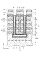
図1は、本実施形態に係る不揮発性半導体記憶装置の特徴を模式的に例示する図であり、
図2は、本実施形態に係る不揮発性半導体記憶装置を例示する斜視図であり、
図3は、本実施形態に係る不揮発性半導体記憶装置を例示する断面図であり、
図4は、本実施形態に係る不揮発性半導体記憶装置のメモリストリングを例示する回路図であり、
図5は、本実施形態に係る不揮発性半導体記憶装置の電極膜を例示する平面図であり、
図6は、本実施形態に係る不揮発性半導体記憶装置の駆動回路を例示する回路図である。
なお、図1及び図2においては、図を見やすくするために、導電部分のみを図示し、絶縁部分は図示を省略している。後述する図10についても同様である。また、図2においては、図示の便宜上、シリコンピラーはZ方向の位置に拘わらず同じ太さで描かれている。
Hereinafter, embodiments of the present invention will be described with reference to the drawings.
First, a first embodiment of the present invention will be described.
FIG. 1 is a diagram schematically illustrating the characteristics of the nonvolatile semiconductor memory device according to this embodiment.
FIG. 2 is a perspective view illustrating the nonvolatile semiconductor memory device according to this embodiment.
FIG. 3 is a cross-sectional view illustrating the nonvolatile semiconductor memory device according to this embodiment.
FIG. 4 is a circuit diagram illustrating a memory string of the nonvolatile semiconductor memory device according to this embodiment.
FIG. 5 is a plan view illustrating an electrode film of the nonvolatile semiconductor memory device according to this embodiment.
FIG. 6 is a circuit diagram illustrating a drive circuit of the nonvolatile semiconductor memory device according to this embodiment.
In FIGS. 1 and 2, only the conductive portion is shown and the insulating portion is not shown in order to make the drawing easy to see. The same applies to FIG. 10 described later. In FIG. 2, for convenience of illustration, the silicon pillar is drawn with the same thickness regardless of the position in the Z direction.
先ず、本実施形態の特徴部分を概略的に説明する。
図1に示すように、本実施形態に係る不揮発性半導体記憶装置1の特徴は、シリコンピラー31と制御ゲート電極CGとの交差部分にメモリトランジスタが設けられた一括加工型の3次元積層型記憶装置において、制御ゲート電極CGに駆動電位を供給する駆動回路41が、貫通している貫通ホールの径が小さい制御ゲート電極CGほど、シリコンピラー31との間の電位差が小さくなるような駆動電位を印加することである。より具体的には、不揮発性半導体記憶装置1においては、下段に配置された制御ゲート電極CGほど、シリコンピラー31が埋設される貫通ホールの径が小さくなっているため、駆動回路41は、下段に配置された制御ゲート電極CGに対してほど、低い駆動電位を印加する。
First, the characteristic part of this embodiment is demonstrated roughly.
As shown in FIG. 1, the nonvolatile
次に、この不揮発性半導体記憶装置の構成を詳細に説明する。
図2及び図3に示すように、本実施形態に係る不揮発性半導体記憶装置1(以下、単に「装置1」ともいう)においては、シリコン基板11が設けられている。シリコン基板11には、メモリセルが形成されるメモリセル領域と、駆動回路が形成される周辺回路領域(図示せず)とが設定されている。周辺回路領域は、メモリセル形成領域の周囲に配置されている。
Next, the configuration of this nonvolatile semiconductor memory device will be described in detail.
As shown in FIGS. 2 and 3, the nonvolatile semiconductor memory device 1 (hereinafter also simply referred to as “
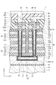
先ず、メモリセル領域について説明する。
メモリセル領域の特徴は、メモリセルが3次元的に配列された積層体MLが設けられており、積層体MLを貫く貫通ホール21の直径が、下方に行くほど細くなっていることである。以下、メモリセル領域の構成を詳細に説明する。
First, the memory cell region will be described.
A feature of the memory cell region is that a stacked body ML in which memory cells are arranged in a three-dimensional manner is provided, and the diameter of the through
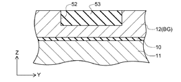
メモリセル領域においては、シリコン基板11上に絶縁膜10が設けられており、その上に導電膜、例えば、ポリシリコン膜12が形成されており、これがバックゲートBGとなっている。バックゲートBG上においては、それぞれ複数の電極膜14と絶縁膜15とが交互に積層されて、積層体MLが構成されている。
In the memory cell region, an
以下、本明細書においては、説明の便宜上、XYZ直交座標系を導入する。この座標系においては、シリコン基板11の上面に平行な方向であって相互に直交する2方向をX方向及びY方向とし、X方向及びY方向の双方に対して直交する方向、すなわち各層の積層方向をZ方向とする。
Hereinafter, in this specification, for convenience of explanation, an XYZ orthogonal coordinate system is introduced. In this coordinate system, two directions that are parallel to the upper surface of the
電極膜14は例えばポリシリコンにより形成されている。積層体MLにおけるX方向中央部においては、電極膜14はY方向に沿って分断され、X方向に延びる複数本の制御ゲート電極CGとなっている。上方、すなわち、Z方向から見て、各層の電極膜14は同じパターンでパターニングされている。なお、後述するように、積層体MLにおけるX方向両端部においては、電極膜14はY方向に沿っては分断されておらず、1対の櫛状の形状をなしている。一方、絶縁膜15は例えばシリコン酸化物(SiO2)からなり、電極膜14同士を絶縁する層間絶縁膜として機能する。
The
積層体ML上には、絶縁膜16、導電膜17及び絶縁膜18がこの順に成膜されている。導電膜17は例えばポリシリコンからなり、Y方向に沿って分断され、X方向に延びる複数本の選択ゲート電極SGとなっている。選択ゲート電極SGは、最上層の制御ゲート電極CGの直上域に2本ずつ設けられている。すなわち、選択ゲート電極SGは制御ゲート電極CGと同じ方向(X方向)に延びているが、配列周期は半分である。なお、後述するように、選択ゲート電極SGには、ビット線側の選択ゲート電極SGbとソース線側の選択ゲート電極SGsとがある。
On the stacked body ML, an insulating
絶縁膜18上には絶縁膜19が設けられており、絶縁膜19上には、X方向に延びるソース線SLが設けられている。ソース線SLは、Y方向に沿って配列された最上層の制御ゲート電極CGのうち、1つおきの制御ゲート電極CGの直上域に配置されている。また、絶縁膜19上には、ソース線SLを覆うように絶縁膜20が設けられており、絶縁膜20上には、Y方向に延びる複数本のビット線BLが設けられている。ソース線SL及びビット線BLは、それぞれ金属膜により形成されている。
An insulating
そして、積層体MLを貫くように、各層の積層方向(Z方向)に延びる複数本の貫通ホール21が形成されている。Z方向から見て、貫通ホール21の形状は例えば円形である。一方、貫通ホール21の側面は垂直方向に対して傾斜しており、貫通ホール21は下方にいくほど細くなっている。各貫通ホール21は各段の制御ゲート電極CGを貫き、下端はバックゲートBGに到達している。また、貫通ホール21はX方向及びY方向に沿ってマトリクス状に配列されている。そして、制御ゲート電極CGはX方向に延びているため、X方向に配列された複数本の貫通ホール21は、同一の制御ゲート電極CGを貫いている。また、Y方向における貫通ホール21の配列周期は、制御ゲート電極CGの配列周期の半分である。これにより、Y方向に配列された貫通ホール21は2個で1組となり、同じ組に属する貫通ホール21は同じ制御ゲート電極CGを貫いている。
A plurality of through
また、バックゲートBGの上層部分内には、1本の貫通ホール21の下端部を、この貫通ホール21から見てY方向に1列分離隔した他の1本の貫通ホール21の下端部に連通させるように、連通孔22が形成されている。これにより、Y方向において隣り合う1対の貫通ホール21と、それらを相互に連通させる連通孔22とにより、1本の連続したU字孔23が形成されている。積層体ML内には、複数本のU字孔23が形成されている。
In addition, in the upper layer portion of the back gate BG, the lower end portion of one through
U字孔23の内面上には、例えばシリコン窒化物からなるバリア膜(図示せず)を介して、ONO膜(Oxide Nitride Oxide film:酸化物−窒化物−酸化物膜)24が設けられている。ONO膜24においては、外側から順に、絶縁性のブロック膜25、電荷蓄積膜26、絶縁性のトンネル膜27が積層されている。ブロック膜25は、装置1の駆動電圧の範囲内にある電圧が印加されても実質的に電流を流さない膜であり、例えば、誘電率が電荷蓄積膜26を形成する材料の誘電率よりも高い高誘電率材料によって形成されており、例えば、シリコン酸化物によって形成されている。電荷蓄積膜26は、電荷をトラップする能力がある膜であり、例えば、シリコン窒化物により形成されている。トンネル膜27は、通常は絶縁性であるが、装置1の駆動電圧の範囲内にある所定の電圧が印加されるとトンネル電流を流す膜であり、例えばシリコン酸化物により形成されている。U字孔23の内面上の全領域において、ONO膜24の膜厚はほぼ均一である。
On the inner surface of the
また、U字孔23の内部には、不純物がドープされた半導体材料、例えば、ポリシリコンが埋め込まれている。これにより、U字孔23の内部には、U字シリコン部材33が設けられている。U字シリコン部材33のうち、貫通ホール21内に位置する部分はシリコンピラー31となっており、連通孔22内に位置する部分は接続部材32となっている。シリコンピラー31の形状はZ方向に延びる柱状であり、例えば円柱状である。但し、上述の如く、貫通ホール21の直径は下方にいくほど細くなっているため、その内部に埋め込まれたシリコンピラー31の直径も、下方にいくほど細くなっている。また、接続部材32の形状はY方向に延びる柱形であり、例えば四角柱形である。U字シリコン部材33を構成する2本のシリコンピラー31及び1本の接続部材32は一体的に形成されており、従って、U字シリコン部材33は、その長手方向に沿って切れ目無く連続的に形成されている。更に、U字シリコン部材33は、ONO膜24によってバックゲートBG及び制御ゲート電極CGから絶縁されている。
The
また、絶縁膜16、選択ゲート電極SG及び絶縁膜18には、複数の貫通ホール51が形成されている。各貫通ホール51は各貫通ホール21の直上域に形成されており、各貫通ホール21に連通されている。ここで、選択ゲート電極SGはX方向に延びているため、X方向に配列された貫通ホール51は、同一の選択ゲート電極SGを貫いている。また、Y方向における貫通ホール51の配列周期は、選択ゲート電極SGの配列周期と同じであり、配列の位相も同じである。従って、Y方向に配列された複数本の貫通ホール51は、選択ゲート電極SGと1対1で対応し、相互に異なる選択ゲート電極SGを貫いている。
A plurality of through
貫通ホール51の内面上には、ゲート絶縁膜28が形成されている。また、貫通ホール51の内部には、例えばポリシリコンが埋め込まれており、シリコンピラー34となっている。シリコンピラー34の形状は、Z方向に延びる柱形であり、例えば円柱形である。シリコンピラー34の下端部は、その直下域に形成されたシリコンピラー31の上端部に接続されている。更に、シリコンピラー34は、ゲート絶縁膜28によって制御ゲート電極SGから絶縁されている。そして、U字シリコン部材33と、その上端部に接続された1対のシリコンピラー34により、U字ピラー30が構成されている。
A
以下、U字ピラー30と、制御ゲート電極CG、選択ゲート電極SG、ソース線SL及びビット線BLとの位置関係を説明する。U字ピラー30は、Y方向において隣り合う1対のシリコンピラー34及び31が、接続部材32によって相互に接続されて構成されている。一方、制御ゲート電極CG、選択ゲート電極SG及びソース線SLはX方向に延びており、ビット線BLはY方向に延びている。そして、U字ピラー30と制御ゲート電極CGのY方向における配列周期は同じであるが、位相が半周期分ずれているため、各U字ピラー30に属する1対のシリコンピラー31、すなわち、接続部材32によって相互に接続された2本のシリコンピラー31は、相互に異なる制御ゲート電極CGを貫いている。一方、Y方向において隣り合う2本のU字ピラー30に属する2本のシリコンピラー31であって、隣り合う2本のシリコンピラー31は、共通の制御ゲート電極CGを貫いている。
Hereinafter, the positional relationship between the
また、Y方向に配列された複数本のシリコンピラー34は相互に異なる選択ゲートSGを貫いており、従って、各U字ピラー30に属する1対のシリコンピラー34も、相互に異なる選択ゲート電極SGを貫いている。一方、X方向に配列された複数本のU字ピラー30は、共通の1対の選択ゲートSGを貫いている。
Further, the plurality of
更に、各U字ピラー30に属する1対のシリコンピラー34のうち、1本のシリコンピラー34は絶縁膜19内に埋設されたソースプラグSPを介してソース線SLに接続されており、他の1本のシリコンピラー34は絶縁膜19及び20内に埋設されたビットプラグBPを介してビット線BLに接続されている。従って、U字ピラー30は、ビット線BLとソース線SLとの間に接続されている。図1乃至図4においては、U字ピラー30が貫く選択ゲート電極SGのうち、ビット線側に配置された選択ゲート電極SGを選択ゲート電極SGbと表記し、ソース線側に配置された選択ゲート電極SGを選択ゲート電極SGsと表記する。そして、X方向に配列されたU字ピラー30は、共通のソース線SLに接続され、相互に異なるビット線BLに接続されている。ここで、X方向におけるU字ピラー30の配列周期は、ビット線BLの配列周期と同じであるため、X方向において、U字ピラー30とビット線BLとは1対1で対応している。一方、Y方向に配列されたU字ピラー30は、2本1組で各ソース線SLに接続され、共通のビット線BLに接続されている。
Further, of the pair of
そして、図1乃至図4に示すように、装置1においては、シリコンピラー31がチャネルとして機能し、制御ゲート電極CGがゲート電極として機能することにより、シリコンピラー31と制御ゲート電極CGとの交差部分に、縦型のメモリトランジスタ35が形成される。各メモリトランジスタ35は、シリコンピラー31と制御ゲート電極CGとの間に配置された電荷蓄積膜26に電子を蓄積することにより、メモリセルとして機能する。積層体ML内には、複数本のシリコンピラー31がX方向及びY方向に沿ってマトリクス状に配列されているため、複数のメモリトランジスタ35が、X方向、Y方向、Z方向に沿って、3次元的に配列される。
As shown in FIGS. 1 to 4, in the
また、シリコンピラー34と選択ゲート電極SGとの交差部分には、シリコンピラー34をチャネルとし、選択ゲート電極SGをゲート電極とし、ゲート絶縁膜28をゲート絶縁膜とした選択トランジスタ36が形成される。この選択トランジスタ36も、上述のメモリトランジスタ35と同様に、縦型トランジスタである。
A
更に、接続部材32とバックゲートBGとの間には、ONO膜24が介在するため、接続部材32をチャネルとし、バックゲートBGをゲート電極とし、ONO膜24をゲート絶縁膜としたバックゲートトランジスタ37が形成される。すなわち、バックゲートBGは、電界によって接続部材32の導通状態を制御する電極として機能する。
Further, since the
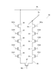
この結果、図4に示すように、各U字ピラー30に沿って、ビット線BLとソース線SLとの間に接続されたメモリストリング38が構成される。メモリストリング38においては、両端部に選択トランジスタ36が設けられ、中央部にバックゲートトランジスタ37が設けられ、各選択トランジスタ36とバックゲートトランジスタ37との間に、電極膜14の積層数と同数のメモリトランジスタ35が直列に接続される。すなわち、積層体ML内に3次元的に配列された複数のメモリトランジスタ35は、U字シリコン部材33毎にメモリストリング38としてまとめられる。
As a result, as shown in FIG. 4, a
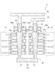
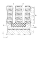
そして、図5に示すように、装置1のメモリセル形成領域は、複数のブロック50に分けられている。以下、ブロック50と各導電部材との位置関係について説明する。
図5に示すように、メモリセル形成領域において設定された複数のブロック50は、Y方向に沿って配列されている。そして、装置1に設けられた導電部材のうち、X方向に延びる導電部材、すなわち、制御ゲート電極CG及び選択ゲート電極SGと、Z方向に延びるU字ピラー30は、ブロック50毎に組分けされている。また、XY平面に沿って形成されているバックゲートBGは、ブロック50毎に分割されており、相互に電気的に分離されている。一方、Y方向に延びるビット線BLは、全てのブロック50を通過するように延びており、全てのブロック50で共有されている。更にまた、シリコン基板11におけるブロック50間の領域には、素子分離膜(図示せず)が形成されている。
As shown in FIG. 5, the memory cell formation region of the
As shown in FIG. 5, the plurality of
また、各ブロック50に属する制御ゲート電極CGは、更に2つのグループに組分けされている。すなわち、制御ゲート電極CGは、ソース線SLの直下域に配置され、上端部がソース線SLに接続されたシリコンピラーによって貫かれた制御ゲート電極CG(図5では「制御ゲート電極CGs」と表記する)と、ソース線SLの直下域から外れた領域に配置され、上端部がビット線BLに接続されたシリコンピラーによって貫かれた制御ゲート電極CG(図5では「制御ゲート電極CGb」と表記する)とに分かれている。そして、制御ゲート電極CGsと制御ゲート電極CGbとはY方向に沿って交互に配列されており、制御ゲート電極CGs同士は共通接続されており、制御ゲート電極CGb同士も共通接続されている。また、制御ゲート電極CGsと制御ゲート電極CGbとは電気的に分離されている。
Further, the control gate electrodes CG belonging to each
具体的には、図5に示すように、電極膜14(図1参照)は、積層体MLのX方向両端部においてはY方向に沿って分断されておらず、X方向に延びる切込が断続的に形成されている。これにより、各ブロック50において、電極膜14は相互に噛み合った1対の櫛状のパターンに分割されており、それぞれ、制御ゲート電極CGs及び制御ゲート電極CGbとなっている。なお、図5においては、図を簡略化するために、制御ゲート電極CGsの櫛の歯は3本とし、制御ゲートCGbの櫛の歯は2本としているが、本実施形態はこれに限定されず、櫛の歯の数はより多くてもよい。
Specifically, as shown in FIG. 5, the electrode film 14 (see FIG. 1) is not divided along the Y direction at both ends in the X direction of the multilayer body ML, and there is a notch extending in the X direction. It is formed intermittently. As a result, in each
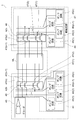
次に、周辺回路領域について説明する。
図6に示すように、周辺回路領域においては、メモリストリング38を駆動する駆動回路41が設けられている。駆動回路41においては、積層体MLに形成された各段の制御ゲート電極CGb及び選択ゲート電極SGbに対して駆動電位を印加する電位供給部42bと、各段の制御ゲート電極CGs及び選択ゲート電極SGsに対して駆動電位を印加する電位供給部42sと、制御信号を出力するデコーダ43とが設けられている。
Next, the peripheral circuit area will be described.
As shown in FIG. 6, a
電位供給部42bには、ポンプ回路部44が設けられている。ポンプ回路部44には、n個のポンプ回路45(1)〜45(n)が設けられている。nは電極膜14の段数である。各ポンプ回路45は、供給された電圧を所定量だけ昇圧させる回路であり、その昇圧量はポンプ回路毎に異なっている。
A
また、電位供給部42bには、スイッチ回路部46が設けられている。スイッチ回路部46においては、n個のスイッチ素子47(1)〜47(n)が設けられている。kを1〜nの整数とするとき、スイッチ素子47(k)は、一端がポンプ回路45(k)に接続され、他端が積層体MLの下からk段目の制御ゲート電極CGbに接続されており、デコーダ43から出力される制御信号に基づいて、ポンプ回路45(k)を下からk段目の制御ゲート電極CGbに接続するか否かを切り替える。例えば、各スイッチ素子47はMOSFETにより形成されており、ソース・ドレインの一方がポンプ回路45に接続され、他方が制御ゲート電極CGbに接続され、ゲートがデコーダ43の出力端子に共通接続されている。これにより、デコーダ43から所定の制御信号が出力されている期間だけ、ポンプ回路45を制御ゲート電極CGbに接続する。
In addition, a
電位供給部42sの構成も、電位供給部42bと同様である。すなわち、電位供給部42sにもポンプ回路部44及びスイッチ回路部46が設けられており、デコーダ43から出力される制御信号に基づいて、各スイッチ素子47が各ポンプ回路45を各制御ゲート電極CGsに接続する。
The configuration of the
次に、上述の如く構成された本実施形態に係る不揮発性半導体記憶装置1の動作について説明する。
図7は、本実施形態に係る不揮発性半導体記憶装置の動作において、各電極及び配線に印加する電位を例示する図であり、
図8は、本実施形態に係る不揮発性半導体記憶装置の動作において、各段の制御ゲート電極に印加する電位を例示する図であり、
図9は、横軸に貫通ホールの直径をとり、縦軸に制御ゲート電極とシリコンピラーとの間の電圧差をとって、印加電位の決定方法を例示するグラフ図である。
Next, the operation of the nonvolatile
FIG. 7 is a diagram illustrating potentials applied to each electrode and wiring in the operation of the nonvolatile semiconductor memory device according to this embodiment.
FIG. 8 is a diagram illustrating potentials applied to the control gate electrodes of the respective stages in the operation of the nonvolatile semiconductor memory device according to this embodiment.
FIG. 9 is a graph illustrating the method for determining the applied potential, with the diameter of the through hole on the horizontal axis and the voltage difference between the control gate electrode and the silicon pillar on the vertical axis.
以下の説明では、メモリトランジスタ35はnチャネル型の電界効果トランジスタであるものとする。また、メモリトランジスタ35において、電荷蓄積膜26に電子が蓄積され、閾値が正にシフトした状態を値「0」とし、電荷蓄積膜26に電子が蓄積されておらず、閾値がシフトしていない状態を値「1」とする。更に、制御ゲート電極の段数(n)は4であるものとし、データの書込及び読出の対象となるメモリトランジスタ35(以下、「選択セル」という)は、上端部がビット線BLに接続されたシリコンピラーにおける下から3段目のメモリトランジスタであるものとする。すなわち、下から3段目の制御ゲート電極CGbが選択セルのゲート電極となる。更にまた、初期状態においては、全てのメモリトランジスタ35に電子が蓄積されておらず、従って、値「1」が書き込まれているものとする。
In the following description, it is assumed that the
(書込動作)
先ず、各メモリトランジスタ35に任意のデータを書き込む書込動作について説明する。データの書込は、1ブロックずつ順番に、X方向に配列された複数個の選択セルに対して同時に行う。図2に示すように、これらの複数個の選択セルは、相互に異なるメモリストリング38に属しているが、同一の制御ゲート電極CGを共有している。また、これらの選択セルが属する複数本のメモリストリング38は、相互に異なるビット線BLに接続されているが、共通の選択ゲート電極SGを貫いており、共通のソース線SLに接続されている。
(Write operation)
First, a write operation for writing arbitrary data to each
先ず、書込対象となるメモリトランジスタ35(選択セル)が属するメモリストリング38(以下、「選択ストリング」という)のY座標を選択する。具体的には、図7に示すように、駆動回路41が選択ストリングの選択ゲート電極SGbに対して選択ゲート電位Vsgを印加し、選択ゲート電極SGsに対してオフ電位Voffを印加する。また、駆動回路41は、非選択のメモリストリング38の選択ゲート電極SGb及びSGsに対してオフ電位Voffを印加する。オフ電位Voffとは、そのゲート電極が構成するトランジスタがオフ状態となるような電位であり、例えば、基準電位Vssである。基準電位Vssは、例えば接地電位(0V)である。選択ゲート電位Vsgとは、その選択ゲート電極SGが構成する選択トランジスタ36の導通状態が、シリコンピラーの電位(ボディ電位)によって決定されるような電位であり、例えば、基準電位Vssよりも高い電位である。更に、バックゲートBGの電位はオン電位Vonとする。オン電位Vonとは、そのゲート電極が構成するトランジスタがオン状態となるような電位であり、例えば、電源電位Vdd(例えば、3.0V)である。
First, the Y coordinate of the memory string 38 (hereinafter referred to as “selected string”) to which the memory transistor 35 (selected cell) to be written belongs is selected. Specifically, as illustrated in FIG. 7, the
これにより、選択ストリングのビット線側の選択トランジスタ36は、ビット線BLの電位によってオン状態とオフ状態とが切り替わる状態となり、ソース線側の選択トランジスタ36はオフ状態となる。また、非選択のメモリストリング38の選択トランジスタ36は全てオフ状態となる。更に、全てのメモリストリング38のバックゲートトランジスタ37がオン状態となる。
As a result, the
次に、ビット線BLのうち、値「0」を書き込む選択セルが接続されたビット線BLには基準電位Vss(例えば、0V)を印加し、値「1」を書き込む選択セルが接続されたビット線BLには電源電位Vdd(例えば、3.0V)を印加する。一方、全てのソース線SLに電源電位Vddを印加する。 Next, a reference potential Vss (for example, 0 V) is applied to the bit line BL of the bit line BL to which the selected cell that writes the value “0” is connected, and the selected cell that writes the value “1” is connected. A power supply potential Vdd (for example, 3.0 V) is applied to the bit line BL. On the other hand, the power supply potential Vdd is applied to all the source lines SL.
この状態で、選択ストリングにおける選択セルの位置を選択する。具体的には、駆動回路41が、選択セルを構成する制御ゲート電極CG、例えば、下から3層目の制御ゲート電極CGbの電位を書込電位Vpgm(例えば、18V)に昇圧させ、それ以外の制御ゲート電極CG、すなわち、3段目以外の制御ゲート電極CGb及び全ての制御ゲート電極CGsの電位を中間電位Vpass(例えば、10V)とする。このとき、3層目の制御ゲート電極CGb同士は互いに接続されているため、非選択のメモリストリングにおいても、3層目の制御ゲート電極CGbには書込電位Vpgmが印加される。書込電位Vpgmは、シリコンピラー31からONO膜24の電荷蓄積膜26に対して電子を注入することができる十分に高い電位であり、基準電位Vss及び選択ゲート電位Vsgよりも高い電位である。すなわち、Vss<Vsg<Vpgmである。また、中間電位Vpassは基準電位Vssよりは高い電位であるが、書込電位Vpgmよりは低い電位である。すなわち、Vss<Vpass<Vpgmである。但し、後述するように、書込電位Vpgmの値は、印加対象とする制御ゲート電極CGが配置されている段によって異ならせる。
In this state, the position of the selected cell in the selected string is selected. Specifically, the
これにより、値「0」を書き込む選択セルについては、ビット線BLの電位が基準電位Vss(例えば、0V)であり、ビット線側の選択ゲート電極SGbの電位が基準電位Vssよりも高い選択ゲート電位Vsgであるため、ビット線側の選択トランジスタ36のソース電位とゲート電位との電位差が閾値を超え、この選択トランジスタ36はオン状態となる。この結果、選択セルのボディ電位Vbodyは基準電位Vssに近くなる。また、選択セルの制御ゲート電極CGの電位は書込電位Vpgm(例えば、18V)である。従って、選択セルにおけるゲート電位とボディ電位との差(Vpgm−Vbody)は十分に大きくなり、この電位差によって高温の電子が生成され、シリコンピラー31からトンネル膜27を介して電荷蓄積膜26に注入される。これにより、この選択セルに値「0」が書き込まれる。
Thereby, for the selected cell to which the value “0” is written, the potential of the bit line BL is the reference potential Vss (for example, 0 V), and the potential of the selection gate electrode SGb on the bit line side is higher than the reference potential Vss. Since the potential is V sg , the potential difference between the source potential and the gate potential of the
一方、値「1」を書き込む選択セルについては、ビット線BLの電位が正電位Vdd(例えば、3.0V)であり、ビット線側の選択ゲート電極SGbの電位が基準電位Vssよりも高い選択ゲート電位Vsgであるため、ビット線側の選択トランジスタ36のソース電位とゲート電位との電位差は小さく、この選択トランジスタ36はバックゲート効果によりオフ状態となる。これにより、シリコンピラー31はフローティング状態となり、選択セルのボディ電位Vbodyは、中間電位Vpass(例えば、10V)が印加された制御ゲート電極CGとのカップリングにより、高い値に維持される。このため、選択セルにおける制御ゲート電極CG3の書込電位Vpgm(例えば、18V)とボディ電位Vbodyとの差(Vpgm−Vbody)は小さくなり、電荷蓄積膜26に電子は注入されない。この結果、この選択セルに値「1」が書き込まれる。
On the other hand, for the selected cell to which the value “1” is written, a selection is made such that the potential of the bit line BL is a positive potential Vdd (eg, 3.0 V) and the potential of the selection gate electrode SGb on the bit line side is higher than the reference potential Vss. Since the gate potential is V sg , the potential difference between the source potential and the gate potential of the
また、非選択のメモリストリング38においては、両端部の選択トランジスタ36が共にオフ状態となるため、シリコンピラー31の電位はフローティング状態となる。この場合、シリコンピラー31のボディ電位Vbodyは、制御ゲート電極CGに印加する電位及びその昇圧レートと、選択ゲート電極SGの電位とにより制御することができ、高い電位に維持することができる。この結果、メモリトランジスタ35におけるゲート電位とボディ電位との差(Vpgm−Vbody)は小さくなり、電荷蓄積膜26には電子が注入されず、元の値が保持される。
In the
このように、本実施形態においては、選択トランジスタの導通状態を制御して書き込む行(Y座標)を選択し、X方向に配列されたメモリストリング38の行単位で順番にデータを書き込む。このとき、制御ゲート電極の電位は、ブロック単位で制御される。このため、書込時のディスターブは、ブロック内のメモリストリングにデータを書き込むために必要な時間の合計量を考慮すればよいことになる。これにより、ブロックサイズを調整することにより、ディスターブ時間を制御することが可能となる。 As described above, in this embodiment, the row (Y coordinate) to be written is selected by controlling the conduction state of the selection transistor, and the data is sequentially written in units of rows of the memory strings 38 arranged in the X direction. At this time, the potential of the control gate electrode is controlled in units of blocks. For this reason, the disturb at the time of writing only needs to consider the total amount of time required for writing data to the memory string in the block. As a result, the disturb time can be controlled by adjusting the block size.
そして、本実施形態においては、図6に示すように、駆動回路41に複数のポンプ回路45が設けられているため、図8に示すように、書込電位Vpgmとして複数水準の電位を生成することができる。そして、デコーダ43が出力する制御信号に基づいて、スイッチ回路部46の各スイッチ素子47が各ポンプ回路45を各段の制御ゲート電極CGに接続することにより、各ポンプ回路45によって生成された書込電位Vpgmを、各段の制御ゲート電極CGに印加することができる。このようにして、書込電位Vpgmの値を、印加対象とする制御ゲート電極CGが配置されている段によって異ならせることができる。
In the present embodiment, a plurality of
すなわち、図8に示すように、下から4段目、すなわち、最上段の制御ゲート電極CG4に印加する書込電位Vpgmの値は(Vpgm0)とし、下から3段目の制御ゲート電極CG3に印加する書込電位Vpgmの値は(Vpgm0)よりも低い(Vpgm0−ΔVpgm1)とし、下から2段目の制御ゲート電極CG2に印加する書込電位Vpgmの値は(Vpgm0−ΔVpgm1)よりも低い(Vpgm0−ΔVpgm2)とし、最下段の制御ゲート電極CG1に印加する書込電位Vpgmの値は(Vpgm0−ΔVpgm2)よりも低い(Vpgm0−ΔVpgm3)とする。なお、0<ΔVpgm1<ΔVpgm2<ΔVpgm3である。
That is, as shown in FIG. 8, the value of the write potential V pgm applied to the control gate electrode CG4 in the fourth stage from the bottom, that is, the top stage is (V pgm 0), and the control gate in the third stage from the bottom The value of the write potential V pgm applied to the electrode CG3 is lower than (V pgm 0) (
仮に、制御ゲート電極CGに印加する電位の値が同じであれば、トンネル膜27に印加される電界の強度は、電荷蓄積膜26の内表面と外表面との面積比が大きいほど強くなる。このため、貫通ホール21の直径が小さいほど、トンネル膜27に印加される電界の強度が強くなる。これにより、値「0」を書き込む予定のメモリトランジスタ35のトンネル膜27に、トンネル効果によって電子電流が流れてしまい、誤って値「1」が書き込まれてしまう誤書込(プログラム・ディスターブ)が発生する可能性がある。また、このような誤書込が発生しない場合でも、貫通ホール21の直径が小さいメモリトランジスタにおいては、シリコンピラー31から電荷蓄積膜26に注入される電子の量が多くなり、電荷蓄積膜26に注入される電荷量が不均一になってしまう。
If the value of the potential applied to the control gate electrode CG is the same, the strength of the electric field applied to the
そこで、本実施形態においては、上述の如く、より下方に位置し、貫通ホール21の直径がより小さいメモリトランジスタほど、書込電位Vpgmとして低い電位を印加する。このとき、シリコンピラー31のボディ電位Vbodyは基準電位Vssに近い電位であるから、より下方に配置されたメモリトランジスタほど、制御ゲート電極CGとシリコンピラー31との間の電位差(Vpgm−Vbody)は小さくなる。そして、電位差(Vpgm−Vbody)が小さいほど、トンネル膜27に印加される電界は弱くなる。
Therefore, in the present embodiment, as described above, a lower potential is applied as the write potential V pgm to a memory transistor that is located further down and has a smaller diameter of the through
このように、本実施形態においては、駆動回路41が、より下方に配置された制御ゲート電極CGほど、より低い書込電位Vpgmを印加することにより、貫通ホール21の直径が小さくなることに起因する電界強度の増加を打ち消し、トンネル膜27に印加される電界強度を均一化することができる。この結果、下方に配置され、貫通ホール21の直径が小さいメモリトランジスタ35においても誤書込(プログラム・ディスターブ)が発生しにくくなる。また、一度の書込動作で各メモリトランジスタ35の電荷蓄積膜26に注入する電子の量を均一にすることができ、メモリトランジスタの駆動を安定させることができる。また、注入される電子の量が均一化されるため、各メモリトランジスタ35に対する書込動作時間も均一化される。これにより、装置1全体の書込動作時間を短縮し、動作速度を向上させることができる。
As described above, in the present embodiment, the
次に、書込電位Vpgmの値の決定方法について説明する。図9に示すように、あるメモリトランジスタにおける貫通ホール21の直径をr(μm)とし、制御ゲート電極CGとシリコンピラー31との間の電位差(Vpgm−Vbody)をVとするとき、電位差Vが下記数式1に従うように、書込電位Vpgmの値を決定すれば、トンネル膜27に印加される電界の強度が均一になる。ここで、下記数式1及び図9に示す電位差Vの値は、貫通ホール21の直径が0.06μm(=60nm)であるときの電位差V(=Vpgm−Vbody)の値を1とした場合の相対値である。下記数式1は、少なくともrの値が0.05〜0.01μmの範囲内において、有効な近似を与える。
Next, a method for determining the value of the write potential V pgm will be described. As shown in FIG. 9, when the diameter of the through
![]()
![]()
(読出動作)
次に、任意のメモリトランジスタ35に書き込まれたデータを読み出す読出動作について説明する。図7に示すように、駆動回路41が、バックゲートBGにオン電位Vonを印加して、バックゲートトランジスタ37をオン状態とする。また、駆動回路41は、選択ストリングの選択ゲート電極SGs及びSGbにオン電位Von(例えば、3.0V)を印加して、選択トランジスタ36をオン状態とする。一方、駆動回路41は、非選択のメモリストリング38の選択ゲート電極SGs及びSGbにはオフ電位Voff(例えば、0V)を印加して、選択トランジスタ36をオフ状態とする。
(Read operation)
Next, a read operation for reading data written in an
そして、駆動回路41が、選択セルの制御ゲート電極CG、すなわち、下から3層目の制御ゲート電極CGbに対して、選択セルの値によって導通状態が異なるような電位を印加する。この電位は、選択セルの値が「0」、すなわち、電荷蓄積膜26に電子が蓄積されていて閾値が正にシフトしている場合はボディに電流が流れず、選択セルの値が「1」、すなわち、電荷蓄積膜26に電子が蓄積されておらず閾値がシフトしていなければボディに電流が流れるような電位であり、例えば、基準電位Vss(例えば、0V)である。また、選択セル以外のメモリトランジスタ35を構成する制御ゲート電極に対して、これらのメモリトランジスタ35がその値によらずオン状態となるような読出電位Vread(例えば、4.5V)を印加する。
Then, the
この状態で、各ビット線BLに電位Vbl(例えば、0.7V)、各ソース線SLに基準電位Vss(例えば、0V)を印加する。この結果、選択セルの値が「1」であれば選択ストリングに電流が流れ、選択セルの値が「0」であれば選択ストリングに電流が流れない。従って、ビット線BLから選択ストリングを介してソース線SLに流れる電流を検出するか、ビット線BLの電位降下を検出することにより、選択セルの値を読み出すことができる。例えば、選択セルの値が「1」であれば、ビット線BLの電位が変化するため、その変化をビット線増幅回路(図示せず)によって増幅して検出し、その検出結果をデータとしてデータバッファー(図示せず)に蓄積する。なお、非選択のメモリストリング38については、選択トランジスタ36がオフ状態であるため、メモリトランジスタ35に記憶された値に拘わらず、電流は流れない。
In this state, a potential Vbl (for example, 0.7 V) is applied to each bit line BL, and a reference potential Vss (for example, 0 V) is applied to each source line SL. As a result, if the value of the selected cell is “1”, current flows in the selected string, and if the value of the selected cell is “0”, no current flows in the selected string. Therefore, the value of the selected cell can be read by detecting the current flowing from the bit line BL to the source line SL via the selected string or by detecting the potential drop of the bit line BL. For example, if the value of the selected cell is “1”, the potential of the bit line BL changes. Therefore, the change is amplified and detected by a bit line amplifier circuit (not shown), and the detection result is used as data. Accumulate in a buffer (not shown). Note that, for the
そして、本実施形態においては、駆動回路41が、ポンプ回路45によって、読出電位Vreadの値を、印加対象とする制御ゲート電極CGが配置されている段によって異ならせる。すなわち、図8に示すように、下から4段目、すなわち、最上段の制御ゲート電極CG4に印加する読出電位Vreadの値は(Vread0)とし、下から3段目の制御ゲート電極CG3に印加する読出電位Vreadの値は(Vread0)よりも低い(Vread0−ΔVread1)とし、下から2段目の制御ゲート電極CG2に印加する読出電位Vreadの値は(Vread0−ΔVread1)よりも低い(Vread0−ΔVread2)とし、最下段の制御ゲート電極CG1に印加する読出電位Vreadの値は(Vread0−ΔVread2)よりも低い(Vread0−ΔVread3)とする。なお、0<ΔVread1<ΔVread2<ΔVread3である。
In this embodiment, the
上述の如く、仮に各制御ゲート電極CGに印加される電位が同じであれば、各メモリトランジスタのトンネル膜27に印加される電界の強度は、貫通ホール21の直径が小さいほど強くなる。そして、読出動作において、トンネル膜27に印加される電界が強くなり過ぎると、トンネル膜27にトンネル効果によって電子電流が流れてしまい、メモリトランジスタに書き込まれている値「0」が値「1」に変化してしまう現象(リード・ディスターブ)が発生する。
As described above, if the potential applied to each control gate electrode CG is the same, the strength of the electric field applied to the
そこで、本実施形態においては、上述の如く、より下方に位置し、貫通ホール21の直径がより小さい制御ゲート電極CGほど、読出電位Vreadとしてより低い電位を印加する。これにより、貫通ホール21の直径が小さくなることに起因する電界強度の増加を、読出電位Vreadを低くすることによって打ち消し、トンネル膜27に印加される電界強度を均一化する。この結果、メモリトランジスタのリード・ディスターブを防止することができる。なお、上述の書込動作の場合と同様な理由により、読出電位Vreadの値は、上記数式1に従って決定することが好ましい。
Therefore, in the present embodiment, as described above, a lower potential is applied as the read potential V read as the control gate electrode CG is positioned lower and the through
(消去動作)
次に、メモリトランジスタに書き込まれたデータを消去する消去動作について説明する。データの消去はブロック単位で行う。図7に示すように、駆動回路41は、バックゲートBGにオン電位Vonを印加して、バックゲートトランジスタ37をオン状態とする。また、消去対象となるブロック(以下、「選択ブロック」ともいう)の全ての制御ゲート電極CGに基準電位Vss(例えば、0V)を印加する。更に、ビット線BL及びソース線SLの電位を消去電位Verase(例えば、15V)に昇圧する。更にまた、選択ゲート電極SGb及びSGsに消去電位Veraseよりも低い選択ゲート電位Vsgを印加する。すなわち、Vsg<Veraseとする。
(Erase operation)
Next, an erase operation for erasing data written in the memory transistor will be described. Data is erased in units of blocks. As illustrated in FIG. 7, the
これにより、ビット線BL及びソース線SLの電位は消去電位Verase(例えば、15V)となり、選択ゲート電極SGb及びSGsの電位は選択ゲート電位Vsgとなるため、ビット線BLと選択ゲート電極SGbとの電位差、及び、ソース線SLと選択ゲート電極SGsとの電位差によるバンド間トンネリングによってホール電流が発生し、シリコンピラー31の電位、すなわち、ボディ電位が昇圧する。一方、消去対象となるブロック(選択ブロック)の制御ゲート電極CGには基準電位Vss(例えば、0V)が印加されているため、シリコンピラー31と制御ゲート電極CGとの間の電位差により、ホールがメモリトランジスタ35の電荷蓄積膜26に注入され、電荷蓄積膜26内の電子が対消滅する。この結果、データが消去される。なお、ホール電流の注入によりボディ電位が上昇するため、電荷蓄積膜26に十分なホールを注入するためには、消去電位Veraseと選択ゲート電位Vsgとの電位差を十分にとる必要があるが、同時に、過剰な電位差により選択トランジスタ36のゲート絶縁膜38が破壊されないように調整する必要がある。
Accordingly, the potentials of the bit line BL and the source line SL become the erase potential V erase (for example, 15 V), and the potentials of the selection gate electrodes SGb and SGs become the selection gate potential V sg , so the bit line BL and the selection gate electrode SGb And a tunneling current between the source line SL and the selection gate electrode SGs, a hole current is generated, and the potential of the
一方、消去対象としないブロック(非選択のブロック)においては、選択ゲート電極SGb及びSGsの電位をビット線BL及びソース線SLの電位に近い電位まで昇圧させて、ビット線BL又はソース線SLに接続された拡散層と選択ゲート電極SGb又はSGsとの間の電界を弱め、ホール電流が発生しないようにする。又は、制御ゲート電極CGの電位をシリコンピラー31と同時に昇圧させて、シリコンピラー31内のホールが電荷蓄積膜26に注入されないようにする。これにより、非選択のブロックにおいては、メモリトランジスタ35に既に書き込まれている値がそのまま保持される。
On the other hand, in a block not to be erased (non-selected block), the potentials of the select gate electrodes SGb and SGs are boosted to a potential close to the potentials of the bit line BL and the source line SL, and the bit line BL or the source line SL is increased. The electric field between the connected diffusion layer and the select gate electrode SGb or SGs is weakened so that no hole current is generated. Alternatively, the potential of the control gate electrode CG is boosted simultaneously with the
消去動作においても、駆動回路41が、下方に配置された選択ゲート電極CGほど、基準電位Vssとしてより高い電位を供給すれば、下方に配置されたメモリトランジスタほど、シリコンピラー31と制御ゲート電極CGとの間の電位差が小さくなり、ONO膜24に印加される電界を均一化することができる。これにより、消去動作時に、貫通ホールの直径が小さいメモリトランジスタに過大な電界が印加され、トンネル効果により制御ゲート電極CGから電荷蓄積膜26に対して電子が注入されることを防止できる。この結果、消去動作に必要なホールの注入、すなわち、シリコンピラー31から電荷蓄積膜26に向かうホールの注入を、制御ゲート電極CGから電荷蓄積膜26に向かう電子の逆注入によって打ち消してしまうことを防止し、消去動作を確実に実施することができる。
Also in the erasing operation, if the
次に、本実施形態の効果について説明する。
本実施形態によれば、上述の如く、駆動回路41に複数のポンプ回路45が設けられており、各ポンプ回路45が各スイッチ素子47を介して各段の制御ゲート電極CGに接続されていることにより、各段の制御ゲート電極CGに対して、相互に異なる駆動電位を印加することができる。これにより、下方に位置し、貫通ホール21の直径が小さいメモリトランジスタほど、制御ゲート電極CGとシリコンピラー31との間の電位差を小さくすることができ、各メモリトランジスタのONO膜24に印加される電界強度を均一化することができる。この結果、メモリトランジスタの誤動作を防止することができる。この技術は、書込動作、読出動作及び消去動作のうち少なくとも1つの動作において、その動作でシリコンピラーとの間の電位差が最も高くなるような電位を制御ゲート電極に対して供給する際に適用すれば、大きな効果を得ることができる。
Next, the effect of this embodiment will be described.
According to the present embodiment, as described above, the
次に、本発明の第2の実施形態について説明する。
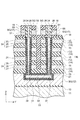
図10は、本実施形態に係る不揮発性半導体記憶装置の特徴を模式的に例示する図である。
図10に示すように、本実施形態においては、貫通ホールが2段構成になっており、各段において、下方に行くほど細くなっている。すなわち、積層体MLは、Z方向に配列された2つの部分積層体ML1及びML2からなり、部分積層体ML1上に部分積層体ML2が積み重ねられている。部分積層体ML1及びML2においては、それぞれ複数枚の絶縁膜15及び電極膜14が積層されている。また、貫通ホール21のうち、部分積層体ML1内に形成された下部21aと、部分積層体ML2内に形成された上部21bは、それぞれ、下方に行くほど細いテーパー状になっている。このため、下部21aの上端部は上部21bの下端部よりも太くなっており、貫通ホール21の内面における下部21aと上部21bとの境界部分には段差が形成されている。
Next, a second embodiment of the present invention will be described.
FIG. 10 is a diagram schematically illustrating the characteristics of the nonvolatile semiconductor memory device according to this embodiment.
As shown in FIG. 10, in this embodiment, the through hole has a two-stage structure, and in each stage, it becomes thinner toward the lower side. That is, the stacked body ML includes two partial stacked bodies ML1 and ML2 arranged in the Z direction, and the partial stacked body ML2 is stacked on the partial stacked body ML1. In the partial stacked bodies ML1 and ML2, a plurality of insulating
そして、駆動回路41は、部分積層体ML1内に配置された複数の電極膜14のうち、下方、すなわち、シリコン基板11側に配置された電極膜14ほど、シリコンピラー31との間の電位差が小さくなるような電位を印加する。同様に、駆動回路41は、部分積層体ML2内に配置された複数の電極膜14のうち、下方に配置された電極膜14ほど、シリコンピラー31との間の電位差が小さくなるような電位を印加する。これにより、本実施形態においても、貫通ホール21の直径の変動に起因する電界強度のばらつきを、駆動電位を異ならせることによって補償することができ、各メモリトランジスタ35のONO膜24に印加される電界強度を均一化することができる。この結果、メモリトランジスタの誤動作を防止することができる。本実施形態における上記以外の構成、動作及び効果は、前述の第1の実施形態と同様である。
The
なお、部分積層体は3段以上積み重ねられていてもよい。この場合、駆動回路41は、各部分積層体内に配置された電極膜14(制御ゲート電極CG)のうち、下方に配置された電極膜ほど、シリコンシリコンピラー31との間の電位差が小さくなるような電位を印加すればよい。
In addition, the partial laminated body may be laminated | stacked 3 or more steps. In this case, in the
次に、本発明の第3の実施形態について説明する。
本実施形態は、前述の第1の実施形態に係る不揮発性半導体記憶装置1の製造方法の実施形態である。
図11乃至図19は、本実施形態に係る不揮発性半導体記憶装置の製造方法を例示する工程断面図である。
なお、図11乃至図19は、図3と同じ断面を示している。
Next, a third embodiment of the present invention will be described.
The present embodiment is an embodiment of a method for manufacturing the nonvolatile
11 to 19 are process cross-sectional views illustrating the method for manufacturing the nonvolatile semiconductor memory device according to this embodiment.
11 to 19 show the same cross section as FIG.
先ず、図11に示すように、シリコン基板11を用意する。このシリコン基板11には、メモリセル形成領域が設定されており、メモリセル形成領域の周囲には周辺回路領域(図示せず)が設定されている。そして、シリコン基板11の上層部分の所定の領域に、素子分離膜を形成する。次に、周辺回路領域において、高耐圧トランジスタのための厚膜ゲート絶縁膜と低耐圧トランジスタのための薄膜ゲート絶縁膜を作り分ける。このとき、メモリセル形成領域においても、シリコン基板11上に絶縁膜10を形成する。
First, as shown in FIG. 11, a
次に、絶縁膜10上に、導電膜としてのポリシリコン膜12を例えば200nmの厚さに堆積させる。そして、メモリセル形成領域において、ポリシリコン膜12の上層部分に対してフォトリソグラフィ及びRIE(Reactive Ion Etching:反応性イオンエッチング)を行い、ポリシリコン膜12の上面にY方向に延びる短冊状の溝52を複数本形成する。溝52はX方向及びY方向に沿ってマトリクス状に配列させる。溝52は、ポリシリコン膜12の上面に形成された凹部である。
Next, a
次に、図12に示すように、例えば、CVD法(Chemical Vapor Deposition法:化学気相成長法)によりシリコン窒化膜を堆積させることにより、ポリシリコン膜12上に犠牲膜53を成膜する。このとき、犠牲膜53は溝52内にも埋め込まれる。次に、犠牲膜53及びポリシリコン膜12を例えばフォトリソグラフィ及びRIEにより加工する。これにより、メモリセル形成領域においてポリシリコン膜12をブロック50(図5参照)毎に分断し、各ブロック50にポリシリコン膜12からなる平板状のバックゲートBGを形成すると共に、周辺回路領域においてポリシリコン膜12からなるゲート電極を形成する。
Next, as shown in FIG. 12, a
その後、周辺回路領域において、シリコン酸化物からなるスペーサを形成し、イオン注入を行って拡散層を形成する。次に、周辺回路領域において、層間絶縁膜を堆積させ、平坦化し、上面がポリシリコン膜12の上面と同じ高さになるようにリセスする。次に、犠牲膜53をリセスして、ポリシリコン膜12上から除去し、溝52の内部のみに残留させる。
Thereafter, a spacer made of silicon oxide is formed in the peripheral circuit region, and ion implantation is performed to form a diffusion layer. Next, in the peripheral circuit region, an interlayer insulating film is deposited and flattened, and the upper surface is recessed so as to be the same height as the upper surface of the
次に、図13に示すように、メモリセル形成領域において、バックゲートBG(ポリシリコン膜12)上に、例えばシリコン酸化物からなる絶縁膜15と、例えばポリシリコンからなる電極膜14とを、交互に堆積させ、積層体MLを形成する。
Next, as shown in FIG. 13, in the memory cell formation region, an insulating
次に、図14に示すように、例えばRIEにより、積層体MLにZ方向に延びる複数本の貫通ホール21を一括で形成する。貫通ホール21はX方向及びY方向に沿ってマトリクス状に配列させる。また、貫通ホール21の底部は溝52内に埋め込まれた犠牲膜53の両端部に到達するようにする。これにより、各犠牲材53に対して、それぞれY方向において隣り合う2本の貫通ホール21を到達させる。更に、Z方向から見て、貫通ホール21の形状は円形とする。このとき、貫通ホール21の内側面は、不可避的にZ方向に対して傾斜したテーパー状になる。この結果、貫通ホール21は、上端部が最も太く、下方に行くほど細くなる逆円錐台形状に形成される。
Next, as illustrated in FIG. 14, a plurality of through
次に、図15に示すように、貫通ホール21を介してウェットエッチングを行い、溝52内の犠牲膜53(図14参照)を除去する。これにより、溝52が連通孔22となり、連通孔22とその両端部に連通された2本の貫通ホール21により、1本の連続したU字孔23が形成される。
Next, as shown in FIG. 15, wet etching is performed through the through
次に、図16に示すように、例えばシリコン窒化物からなるバリア膜(図示せず)を形成した後、シリコン酸化膜、シリコン窒化膜、シリコン酸化膜を連続的に堆積させる。これにより、U字孔23の内面上に、バリア膜を介して、シリコン酸化膜からなるブロック膜25、シリコン窒化膜からなる電荷蓄積膜26、シリコン酸化膜からなるトンネル膜27がこの順に積層され、ONO膜24が形成される。
Next, as shown in FIG. 16, after forming a barrier film (not shown) made of, for example, silicon nitride, a silicon oxide film, a silicon nitride film, and a silicon oxide film are successively deposited. As a result, a
次に、全面にアモルファスシリコンを堆積させる。これにより、U字孔23内にアモルファスシリコンが埋め込まれ、U字シリコン部材33が形成される。U字シリコン部材33は、貫通ホール21内に埋め込まれた1対のシリコンピラー31と、連通孔22内に埋め込まれた1本の接続部材32とから構成される。その後、積層体ML上に堆積されたアモルファスシリコン、シリコン酸化膜、シリコン窒化膜、シリコン酸化膜を除去する。
Next, amorphous silicon is deposited on the entire surface. Thereby, amorphous silicon is embedded in the
次に、図17に示すように、積層体MLを例えばRIEによって加工し、積層体MLに溝54を形成する。溝54は、接続部材32に接続された2本のシリコンピラー31の間の領域をつなぐようにX方向に延び、最下層の絶縁膜15まで到達するように形成する。
Next, as illustrated in FIG. 17, the stacked body ML is processed by, for example, RIE to form a
このとき、図5に示すように、溝54は、電極膜14を相互に噛み合った1対の櫛状のパターンに分断するように形成する。すなわち、積層体MLのX方向中央部においては、溝54はX方向に延びるように形成する。これにより、電極膜14を、X方向に延びる複数本の制御ゲート電極CGに分断する。このとき、Y方向における接続部材32間の領域の直上域には、溝54を形成しない。これにより、各制御ゲート電極CGは、Y方向に沿って配列された2本のシリコンピラー31によって貫通される。また、積層体MLのX方向両端部においては、溝54はX方向には延ばさずに、Y方向に断続的に延びるように形成する。これにより、積層体MLのX方向中央部においてY方向に沿って交互に配置された制御ゲート電極CGb及びCGsが、積層体MLのX方向の各端部において、それぞれ共通接続される。
At this time, as shown in FIG. 5, the
次に、図18に示すように、積層体ML上に絶縁膜16を堆積させて平坦化する。絶縁膜16は溝54内にも埋め込まれる。次いで、例えばアモルファスシリコンからなる導電膜17を堆積し、エッチングしてメモリセル領域のみに残留させる。
Next, as shown in FIG. 18, the insulating
次に、例えば、導電膜17上にレジスト膜(図示せず)を形成し、このレジスト膜をマスクとしたエッチングとレジスト膜のスリミングとを繰り返すことにより、積層体MLを階段状に加工する。これにより、上方(Z方向)から見て、各段の制御ゲート電極CGのX方向両端部がそれより上段の制御ゲート電極CGによって覆われなくなり、後の工程において、上方から各段の制御ゲート電極CGに対してコンタクトを形成することが可能となる。次に、階段状に加工した積層体MLを覆うように、例えばシリコン窒化物からなるエッチングストッパ膜(図示せず)を成膜し、その上に層間絶縁膜(図示せず)を形成し、上面を平坦化する。これにより、積層体MLの周囲が層間絶縁膜によって埋め込まれる。
Next, for example, a resist film (not shown) is formed on the
その後、導電膜17上に絶縁膜18を形成する。そして、絶縁膜18、導電膜17及び絶縁膜16を貫通し、積層体ML内の貫通ホール21の上端に到達するように、貫通ホール51を形成する。
Thereafter, an insulating
次に、図19に示すように、全面に絶縁膜を堆積させ、アモルファスシリコンを堆積させる。そして、アモルファスシリコン及び絶縁膜をエッチバックして、貫通ホール51内にのみ残留させる。これにより、貫通ホール51の内面上にゲート絶縁膜28が形成されると共に、アモルファスシリコンが埋め込まれる。次に、温度が例えば600℃の熱処理を行い、貫通ホール51内のアモルファスシリコンを結晶化させてポリシリコンとする。そして、このポリシリコンに対して、ヒ素(As)を例えば加速電圧を40keV、ドーズ量を3×1015cm−2としてイオン注入し、ドレイン拡散層(図示せず)を形成する。これにより、貫通ホール51内にシリコンピラー34が形成される。シリコンピラー34はシリコンピラー31に接続される。
Next, as shown in FIG. 19, an insulating film is deposited on the entire surface, and amorphous silicon is deposited. Then, the amorphous silicon and the insulating film are etched back to remain only in the through
次に、絶縁膜18及び導電膜17に対してRIE等の加工を行い、Y方向において隣り合うシリコンピラー34間の領域に、X方向に延びる溝55を形成する。これにより、導電膜17をY方向に沿って分断し、X方向に延びる複数本の選択ゲート電極SGを形成する。
Next, processing such as RIE is performed on the insulating
次に、図3に示すように、絶縁膜18上に絶縁膜19を形成し、絶縁膜19内にソースプラグSPを埋設すると共に、絶縁膜19上にX方向に延びるソース線SLを形成する。このとき、ソース線SLはソースプラグSPを介して、一部のシリコンピラー34のドレイン拡散層に接続される。また、積層体MLの周囲に設けられた層間絶縁膜(図示せず)に、上方から各制御ゲート電極CG及び各選択ゲート電極SGに接続されるコンタクト(図示せず)を形成する。次に、絶縁膜19上に、ソース線SLを覆うように絶縁膜20を形成する。次に、絶縁膜20及び19内にビットプラグBPを埋設すると共に、絶縁膜20上にY方向に延びるビット線BLを形成する。このとき、ビット線BLはビットプラグBPを介して、残りのシリコンピラー34のドレイン拡散層に接続される。一方、通常の方法により、周辺回路領域に駆動回路41(図6参照)を形成する。これにより、不揮発性半導体記憶装置1が製造される。
Next, as shown in FIG. 3, an insulating
本実施形態によれば、前述の第1の実施形態に係る不揮発性半導体記憶装置1を製造することができる。そして、本実施形態によれば、駆動回路41が各段の制御ゲート電極CGに相互に異なる電位を供給することにより、各メモリトランジスタ35のONO膜24に印加される電界を均一化するため、貫通ホール21の直径を過剰に均一化する必要がない。このため、貫通ホール21のアスペクト比を大きくすることができ、所定の段数の電極膜14が積層された装置1を製造する際に、貫通ホール21の形成回数を減らすことができ、従って、リソグラフィ工程の回数を減らすことができる。この結果、不揮発性半導体記憶装置1の製造コストを低減することができる。
According to this embodiment, the nonvolatile
なお、上述の積層体MLを形成し、積層体MLに貫通ホール21を形成し、貫通ホール21内にシリコンピラー31を埋め込む一連の工程を2回繰り返すことにより、前述の第2の実施形態に係る不揮発性半導体装置2を製造することができる。また、上述の工程を3回以上繰り返せば、部分積層体が3段以上積み重ねられた不揮発性半導体記憶装置を製造することができる。
Note that the above-described second embodiment is achieved by repeating the series of steps of forming the above-described stacked body ML, forming the through
以上、実施形態を参照して本発明を説明したが、本発明はこれらの実施形態に限定されるものではない。前述の各実施形態に対して、当業者が適宜、構成要素の追加、削除若しくは設計変更を行ったもの、又は、工程の追加、省略若しくは条件変更を行ったものも、本発明の要旨を備えている限り、本発明の範囲に含有される。 While the present invention has been described with reference to the embodiments, the present invention is not limited to these embodiments. Those in which those skilled in the art appropriately added, deleted, or changed the design, or added, omitted, or changed conditions in the above-described embodiments appropriately include the gist of the present invention. As long as it is included, it is included in the scope of the present invention.
例えば、前述の第1の実施形態においては、書込動作、読出動作及び消去動作の全てについて、駆動回路41が各段の制御ゲート電極CGに相互に異なる電位を供給する例を示したが、本発明はこれに限定されず、例えば、書込動作及び読出動作についてのみ、各段の制御ゲート電極に相互に異なる電位を供給してもよい。この場合は、基準電位Vssを共通化することができ、駆動回路を簡略化することができる。また、書込動作、読出動作及び消去動作のうち、いずれか1つの動作についてのみ、各段の制御ゲート電極に相互に異なる電位を供給してもよい。また、制御ゲート電極等の形状は、前述の各実施形態には限定されない。
For example, in the first embodiment described above, an example in which the
1、2 不揮発性半導体記憶装置、10 絶縁膜、11 シリコン基板、12 ポリシリコン膜、14 電極膜、15、16、18、19、20 絶縁膜、17、導電膜、21 貫通ホール、22 連通孔、23 U字孔、24 ONO膜、25 ブロック膜、26 電荷蓄積膜、27 トンネル膜、28 ゲート絶縁膜、30 U字ピラー、31 シリコンピラー、32 接続部材、33 U字シリコン部材、34 シリコンピラー、35 メモリトランジスタ、36 選択トランジスタ、37 バックゲートトランジスタ、38 メモリストリング、41 駆動回路、42b、42s 電位供給部、43 デコーダ、44 ポンプ回路部、 45(1)〜45(n) ポンプ回路、46 スイッチ回路部、47(1)〜47(n) スイッチ素子、50 ブロック、51 貫通ホール、52、54、55 溝、53 犠牲膜、BG バックゲート、BL ビット線、BP ビットプラグ、CG、CGb、CGs 制御ゲート電極、ML 積層体、ML1、ML2 部分積層体、SG、SGb、SGs 選択ゲート電極、SL ソース線、SP ソースプラグ
1, 2 Non-volatile semiconductor memory device, 10 insulating film, 11 silicon substrate, 12 polysilicon film, 14 electrode film, 15, 16, 18, 19, 20 insulating film, 17, conductive film, 21 through hole, 22 communication hole , 23 U-shaped hole, 24 ONO film, 25 block film, 26 charge storage film, 27 tunnel film, 28 gate insulating film, 30 U-pillar, 31 silicon pillar, 32 connecting member, 33 U-shaped silicon member, 34
Claims (5)
前記基板上に設けられ、それぞれ複数の絶縁膜及び電極膜が交互に積層され、積層方向に延びる貫通ホールが形成された積層体と、
前記貫通ホールの内部に埋設された半導体ピラーと、
前記電極膜と前記半導体ピラーとの間に設けられた電荷蓄積膜と、
前記電極膜に対して電位を供給する駆動回路と、
を備え、
前記貫通ホールの径は、前記積層方向における位置によって異なっており、
前記駆動回路は、貫通している前記貫通ホールの径が小さい前記電極膜ほど、前記半導体ピラーとの間の電位差が小さくなるような電位を供給することを特徴とする不揮発性半導体記憶装置。 A substrate,
A laminated body provided on the substrate, each having a plurality of insulating films and electrode films alternately laminated, and having a through hole extending in the laminating direction;
A semiconductor pillar embedded in the through hole;
A charge storage film provided between the electrode film and the semiconductor pillar;
A drive circuit for supplying a potential to the electrode film;
With
The diameter of the through hole differs depending on the position in the stacking direction,
The non-volatile semiconductor memory device, wherein the drive circuit supplies a potential such that a potential difference between the electrode film and the semiconductor pillar is smaller as the diameter of the penetrating hole is smaller.
各前記部分積層体において、前記貫通ホールの径は前記基板に近いほど小さいことを特徴とする請求項1記載の不揮発性半導体記憶装置。 The laminated body has a plurality of partial laminated bodies arranged in the laminating direction and each having a plurality of the insulating films and the electrode films disposed thereon,
2. The nonvolatile semiconductor memory device according to claim 1, wherein in each of the partial stacked bodies, the diameter of the through hole is smaller as it is closer to the substrate.
前記貫通ホールにおける一の前記電極膜を貫通する部分の直径をr(μm)とし、前記半導体ピラーと前記一の電極膜との間の電位差であって、前記直径が0.06μmであるときの電位差を1とした場合の相対電位差をVとするとき、前記駆動回路が前記一の電極膜に対して供給する電位は、下記数式に従って決定されていることを特徴とする請求項1〜3のいずれか1つに記載の不揮発性半導体記憶装置。
The diameter of a portion of the through hole that penetrates the one electrode film is r (μm), and is a potential difference between the semiconductor pillar and the one electrode film, and the diameter is 0.06 μm. 4. The potential supplied to the one electrode film by the drive circuit when the relative potential difference when the potential difference is 1 is V is determined according to the following mathematical formula. The nonvolatile semiconductor memory device according to any one of the above.
前記電極膜に対して電位を印加する際に、貫通している前記貫通ホールの径が小さい前記電極膜ほど、前記半導体ピラーとの間の電位差が小さくなるような電位を供給することを特徴とする不揮発性半導体記憶装置の駆動方法。 A substrate, a stacked body provided on the substrate, each having a plurality of insulating films and electrode films alternately stacked to form a through hole extending in the stacking direction, a semiconductor pillar embedded in the through hole, and the electrode film A nonvolatile semiconductor memory device including a charge storage film provided between the semiconductor pillar and a diameter of the through hole depending on a position in the stacking direction,
When applying a potential to the electrode film, the electrode film having a smaller diameter of the through hole penetrating the electrode film supplies a potential such that a potential difference with the semiconductor pillar is reduced. A method for driving a nonvolatile semiconductor memory device.
Priority Applications (8)
| Application Number | Priority Date | Filing Date | Title |
|---|---|---|---|
| JP2009251891A JP5259552B2 (en) | 2009-11-02 | 2009-11-02 | Nonvolatile semiconductor memory device and driving method thereof |
| US12/851,054 US8218358B2 (en) | 2009-11-02 | 2010-08-05 | Nonvolatile semiconductor memory device and method for driving same |
| KR1020100084677A KR101082228B1 (en) | 2009-11-02 | 2010-08-31 | Nonvolatile semiconductor memory device and method for driving same |
| US14/327,359 USRE45840E1 (en) | 2009-11-02 | 2014-07-09 | Nonvolatile semiconductor memory device and method for driving same |
| US14/992,650 USRE46785E1 (en) | 2009-11-02 | 2016-01-11 | Nonvolatile semiconductor memory device and method for driving same |
| US15/890,143 USRE48191E1 (en) | 2009-11-02 | 2018-02-06 | Nonvolatile semiconductor memory device and method for driving same |
| US16/926,273 USRE49152E1 (en) | 2009-11-02 | 2020-07-10 | Nonvolatile semiconductor memory device and method for driving same |
| US17/850,399 USRE50330E1 (en) | 2009-11-02 | 2022-06-27 | Nonvolatile semiconductor memory device and method for driving same |
Applications Claiming Priority (1)
| Application Number | Priority Date | Filing Date | Title |
|---|---|---|---|
| JP2009251891A JP5259552B2 (en) | 2009-11-02 | 2009-11-02 | Nonvolatile semiconductor memory device and driving method thereof |
Publications (2)
| Publication Number | Publication Date |
|---|---|
| JP2011096340A JP2011096340A (en) | 2011-05-12 |
| JP5259552B2 true JP5259552B2 (en) | 2013-08-07 |
Family
ID=43925293
Family Applications (1)
| Application Number | Title | Priority Date | Filing Date |
|---|---|---|---|
| JP2009251891A Active JP5259552B2 (en) | 2009-11-02 | 2009-11-02 | Nonvolatile semiconductor memory device and driving method thereof |
Country Status (3)
| Country | Link |
|---|---|
| US (6) | US8218358B2 (en) |
| JP (1) | JP5259552B2 (en) |
| KR (1) | KR101082228B1 (en) |
Cited By (1)
| Publication number | Priority date | Publication date | Assignee | Title |
|---|---|---|---|---|
| KR20120131653A (en) * | 2011-05-26 | 2012-12-05 | 에스케이하이닉스 주식회사 | Nonvolatile memory device and method for fabricating the same |
Families Citing this family (41)
| Publication number | Priority date | Publication date | Assignee | Title |
|---|---|---|---|---|
| JP5086959B2 (en) * | 2008-09-26 | 2012-11-28 | 株式会社東芝 | Nonvolatile semiconductor memory device |
| JP5380190B2 (en) * | 2009-07-21 | 2014-01-08 | 株式会社東芝 | Nonvolatile semiconductor memory device and manufacturing method thereof |
| JP5052575B2 (en) * | 2009-09-01 | 2012-10-17 | 株式会社東芝 | Nonvolatile semiconductor memory device |
| JP4913188B2 (en) * | 2009-09-18 | 2012-04-11 | 株式会社東芝 | Nonvolatile semiconductor memory device |
| JP2012059830A (en) * | 2010-09-07 | 2012-03-22 | Toshiba Corp | Semiconductor memory device |
| KR101198253B1 (en) | 2010-12-30 | 2012-11-07 | 에스케이하이닉스 주식회사 | Nonvolatile memory device and method for fabricating the same |
| US8750040B2 (en) | 2011-01-21 | 2014-06-10 | Micron Technology, Inc. | Memory devices having source lines directly coupled to body regions and methods |
| US8431961B2 (en) * | 2011-02-03 | 2013-04-30 | Micron Technology, Inc. | Memory devices with a connecting region having a band gap lower than a band gap of a body region |
| JP2012203969A (en) * | 2011-03-25 | 2012-10-22 | Toshiba Corp | Nonvolatile semiconductor memory device |
| JP2013065636A (en) * | 2011-09-15 | 2013-04-11 | Toshiba Corp | Nonvolatile semiconductor storage device and manufacturing method of the same |
| US9171625B2 (en) | 2012-06-15 | 2015-10-27 | Micron Technology, Inc. | Apparatuses and methods to modify pillar potential |
| JP2014013634A (en) * | 2012-07-03 | 2014-01-23 | Toshiba Corp | Nonvolatile semiconductor memory device and operation method thereof |
| US8754459B2 (en) | 2012-08-31 | 2014-06-17 | Kabushiki Kaisha Toshiba | Semiconductor memory device |
| US8780632B2 (en) | 2012-11-09 | 2014-07-15 | Sandisk Technologies Inc. | De-duplication techniques using NAND flash based content addressable memory |
| US8780634B2 (en) | 2012-11-09 | 2014-07-15 | Sandisk Technologies Inc. | CAM NAND with OR function and full chip search capability |
| US8634248B1 (en) | 2012-11-09 | 2014-01-21 | Sandisk Technologies Inc. | On-device data analytics using NAND flash based intelligent memory |
| US10127150B2 (en) | 2012-11-09 | 2018-11-13 | Sandisk Technologies Llc | Key value addressed storage drive using NAND flash based content addressable memory |
| US8780633B2 (en) | 2012-11-09 | 2014-07-15 | SanDisk Technologies, Inc. | De-duplication system using NAND flash based content addressable memory |
| US8773909B2 (en) | 2012-11-09 | 2014-07-08 | Sandisk Technologies Inc. | CAM NAND with or function and full chip search capability |
| US8817541B2 (en) | 2012-11-09 | 2014-08-26 | Sandisk Technologies Inc. | Data search using bloom filters and NAND based content addressable memory |
| US8792279B2 (en) | 2012-11-09 | 2014-07-29 | Sandisk Technologies Inc. | Architectures for data analytics using computational NAND memory |
| US8811085B2 (en) | 2012-11-09 | 2014-08-19 | Sandisk Technologies Inc. | On-device data analytics using NAND flash based intelligent memory |
| US8780635B2 (en) | 2012-11-09 | 2014-07-15 | Sandisk Technologies Inc. | Use of bloom filter and improved program algorithm for increased data protection in CAM NAND memory |
| US9075424B2 (en) | 2013-03-06 | 2015-07-07 | Sandisk Technologies Inc. | Compensation scheme to improve the stability of the operational amplifiers |
| JP2014183304A (en) | 2013-03-19 | 2014-09-29 | Toshiba Corp | Nonvolatile semiconductor storage device and method for manufacturing the same |
| JP2015176620A (en) * | 2014-03-14 | 2015-10-05 | 株式会社東芝 | semiconductor memory device |
| KR102116674B1 (en) | 2014-03-21 | 2020-06-08 | 삼성전자주식회사 | Nonvolatile memory device and storage device having the same and operation method thereof |
| WO2015189916A1 (en) * | 2014-06-10 | 2015-12-17 | ユニサンティス エレクトロニクス シンガポール プライベート リミテッド | Columnar semiconductor memory device and method for manufacturing same |
| US9698342B2 (en) * | 2014-09-11 | 2017-07-04 | Kabushiki Kaisha Toshiba | Contact layer for magnetic tunnel junction element and manufacturing method thereof |
| JP6309909B2 (en) * | 2015-03-12 | 2018-04-11 | 東芝メモリ株式会社 | Nonvolatile semiconductor memory device |
| JP6290124B2 (en) | 2015-03-12 | 2018-03-07 | 東芝メモリ株式会社 | Semiconductor memory device |
| JP2016225614A (en) | 2015-05-26 | 2016-12-28 | 株式会社半導体エネルギー研究所 | Semiconductor device |
| JP2017107626A (en) * | 2015-12-10 | 2017-06-15 | 株式会社東芝 | Semiconductor device |
| JP6595357B2 (en) * | 2016-02-01 | 2019-10-23 | 東芝メモリ株式会社 | Memory device |
| JP2018045752A (en) | 2016-09-16 | 2018-03-22 | 東芝メモリ株式会社 | Semiconductor device |
| JP2018085160A (en) | 2016-11-25 | 2018-05-31 | 東芝メモリ株式会社 | Semiconductor device and operation method thereof |
| CN106847821B (en) | 2017-03-07 | 2018-09-14 | 长江存储科技有限责任公司 | Semiconductor structure and forming method thereof |
| US10593730B1 (en) * | 2018-10-10 | 2020-03-17 | Micron Technology, Inc. | Three-dimensional memory array |
| KR102723994B1 (en) | 2019-02-27 | 2024-10-30 | 삼성전자주식회사 | Integrated circuit devices |
| US20200365612A1 (en) * | 2019-05-16 | 2020-11-19 | Macronix International Co., Ltd. | Three dimensional memory device and method for fabricating the same |
| US12581666B2 (en) * | 2023-06-01 | 2026-03-17 | Macronix International Co., Ltd. | Memory device based on thyristors |
Family Cites Families (24)
| Publication number | Priority date | Publication date | Assignee | Title |
|---|---|---|---|---|
| US5798966A (en) * | 1997-03-31 | 1998-08-25 | Intel Corporation | Flash memory VDS compensation techiques to reduce programming variability |
| US6631085B2 (en) * | 2000-04-28 | 2003-10-07 | Matrix Semiconductor, Inc. | Three-dimensional memory array incorporating serial chain diode stack |
| US6903977B2 (en) * | 2001-09-25 | 2005-06-07 | Sony Corporation | Nonvolatile semiconductor memory device and method of producing the same |
| US6925007B2 (en) * | 2001-10-31 | 2005-08-02 | Sandisk Corporation | Multi-state non-volatile integrated circuit memory systems that employ dielectric storage elements |
| JP4647175B2 (en) * | 2002-04-18 | 2011-03-09 | ルネサスエレクトロニクス株式会社 | Semiconductor integrated circuit device |
| US7218570B2 (en) * | 2004-12-17 | 2007-05-15 | Sandisk 3D Llc | Apparatus and method for memory operations using address-dependent conditions |
| KR100673170B1 (en) * | 2005-03-10 | 2007-01-22 | 주식회사 하이닉스반도체 | Flash memory device having an improved erase function and a method of controlling the erase operation thereof |
| US7671356B2 (en) * | 2005-11-03 | 2010-03-02 | Elpida Memory, Inc. | Electrically rewritable non-volatile memory element and method of manufacturing the same |
| US7545675B2 (en) * | 2005-12-16 | 2009-06-09 | Sandisk Corporation | Reading non-volatile storage with efficient setup |
| US7436703B2 (en) * | 2005-12-27 | 2008-10-14 | Sandisk Corporation | Active boosting to minimize capacitive coupling effect between adjacent gates of flash memory devices |
| JP5016832B2 (en) * | 2006-03-27 | 2012-09-05 | 株式会社東芝 | Nonvolatile semiconductor memory device and manufacturing method thereof |
| JP4768557B2 (en) * | 2006-09-15 | 2011-09-07 | 株式会社東芝 | Nonvolatile semiconductor memory device and manufacturing method thereof |
| US7532518B2 (en) * | 2007-06-25 | 2009-05-12 | Spansion Llc | Compensation method to achieve uniform programming speed of flash memory devices |
| JP2009087433A (en) * | 2007-09-28 | 2009-04-23 | Toshiba Corp | Nonvolatile semiconductor memory device |
| JP5142692B2 (en) * | 2007-12-11 | 2013-02-13 | 株式会社東芝 | Nonvolatile semiconductor memory device |
| US7961507B2 (en) * | 2008-03-11 | 2011-06-14 | Micron Technology, Inc. | Non-volatile memory with resistive access component |
| KR100991220B1 (en) * | 2008-07-21 | 2010-11-04 | 삼성전자주식회사 | Contact structure in a substrate having an bonded interface, a semiconductor device having the same and methods of manufacturing the same |
| JP5086959B2 (en) | 2008-09-26 | 2012-11-28 | 株式会社東芝 | Nonvolatile semiconductor memory device |
| JP5388537B2 (en) * | 2008-10-20 | 2014-01-15 | 株式会社東芝 | Nonvolatile semiconductor memory device and manufacturing method thereof |
| JP5300419B2 (en) * | 2008-11-05 | 2013-09-25 | 株式会社東芝 | Nonvolatile semiconductor memory device and manufacturing method thereof |
| JP5364342B2 (en) * | 2008-11-10 | 2013-12-11 | 株式会社東芝 | Nonvolatile semiconductor memory device and manufacturing method thereof |
| US9153596B2 (en) * | 2009-02-23 | 2015-10-06 | Cypress Semiconductor Corporation | Adjacent wordline disturb reduction using boron/indium implant |
| JP4913188B2 (en) * | 2009-09-18 | 2012-04-11 | 株式会社東芝 | Nonvolatile semiconductor memory device |
| US11101266B2 (en) * | 2009-10-12 | 2021-08-24 | Monolithic 3D Inc. | 3D device and devices with bonding |
-
2009
- 2009-11-02 JP JP2009251891A patent/JP5259552B2/en active Active
-
2010
- 2010-08-05 US US12/851,054 patent/US8218358B2/en not_active Ceased
- 2010-08-31 KR KR1020100084677A patent/KR101082228B1/en not_active Expired - Fee Related
-
2014
- 2014-07-09 US US14/327,359 patent/USRE45840E1/en active Active
-
2016
- 2016-01-11 US US14/992,650 patent/USRE46785E1/en active Active
-
2018
- 2018-02-06 US US15/890,143 patent/USRE48191E1/en active Active
-
2020
- 2020-07-10 US US16/926,273 patent/USRE49152E1/en active Active
-
2022
- 2022-06-27 US US17/850,399 patent/USRE50330E1/en active Active
Cited By (2)
| Publication number | Priority date | Publication date | Assignee | Title |
|---|---|---|---|---|
| KR20120131653A (en) * | 2011-05-26 | 2012-12-05 | 에스케이하이닉스 주식회사 | Nonvolatile memory device and method for fabricating the same |
| KR101868799B1 (en) | 2011-05-26 | 2018-06-21 | 에스케이하이닉스 주식회사 | Nonvolatile memory device and method for fabricating the same |
Also Published As
| Publication number | Publication date |
|---|---|
| USRE46785E1 (en) | 2018-04-10 |
| USRE45840E1 (en) | 2016-01-12 |
| JP2011096340A (en) | 2011-05-12 |
| KR101082228B1 (en) | 2011-11-09 |
| US20110103153A1 (en) | 2011-05-05 |
| KR20110048452A (en) | 2011-05-11 |
| USRE49152E1 (en) | 2022-07-26 |
| USRE50330E1 (en) | 2025-03-04 |
| USRE48191E1 (en) | 2020-09-01 |
| US8218358B2 (en) | 2012-07-10 |
Similar Documents
| Publication | Publication Date | Title |
|---|---|---|
| JP5259552B2 (en) | Nonvolatile semiconductor memory device and driving method thereof | |
| JP5383241B2 (en) | Nonvolatile semiconductor memory device and manufacturing method thereof | |
| JP5297342B2 (en) | Nonvolatile semiconductor memory device | |
| JP5112201B2 (en) | Nonvolatile semiconductor memory device | |
| KR101076125B1 (en) | Nonvolatile semiconductor memory device | |
| JP5388600B2 (en) | Method for manufacturing nonvolatile semiconductor memory device | |
| KR101267130B1 (en) | Operating method of semiconductor memory device | |
| KR100964759B1 (en) | Non-volatile semiconductor memory device | |
| JP2007317874A (en) | Nonvolatile semiconductor memory device | |
| US9978770B2 (en) | Semiconductor memory device |
Legal Events
| Date | Code | Title | Description |
|---|---|---|---|
| A621 | Written request for application examination |
Free format text: JAPANESE INTERMEDIATE CODE: A621 Effective date: 20120305 |
|
| A977 | Report on retrieval |
Free format text: JAPANESE INTERMEDIATE CODE: A971007 Effective date: 20130311 |
|
| TRDD | Decision of grant or rejection written | ||
| A01 | Written decision to grant a patent or to grant a registration (utility model) |
Free format text: JAPANESE INTERMEDIATE CODE: A01 Effective date: 20130403 |
|
| A61 | First payment of annual fees (during grant procedure) |
Free format text: JAPANESE INTERMEDIATE CODE: A61 Effective date: 20130424 |
|
| FPAY | Renewal fee payment (event date is renewal date of database) |
Free format text: PAYMENT UNTIL: 20160502 Year of fee payment: 3 |
|
| R151 | Written notification of patent or utility model registration |
Ref document number: 5259552 Country of ref document: JP Free format text: JAPANESE INTERMEDIATE CODE: R151 |
|
| S111 | Request for change of ownership or part of ownership |
Free format text: JAPANESE INTERMEDIATE CODE: R313111 |
|
| R350 | Written notification of registration of transfer |
Free format text: JAPANESE INTERMEDIATE CODE: R350 |
|
| S111 | Request for change of ownership or part of ownership |
Free format text: JAPANESE INTERMEDIATE CODE: R313111 |
|
| R350 | Written notification of registration of transfer |
Free format text: JAPANESE INTERMEDIATE CODE: R350 |