JP5173234B2 - 放射線撮像装置及び放射線撮像システム - Google Patents
放射線撮像装置及び放射線撮像システム Download PDFInfo
- Publication number
- JP5173234B2 JP5173234B2 JP2007099751A JP2007099751A JP5173234B2 JP 5173234 B2 JP5173234 B2 JP 5173234B2 JP 2007099751 A JP2007099751 A JP 2007099751A JP 2007099751 A JP2007099751 A JP 2007099751A JP 5173234 B2 JP5173234 B2 JP 5173234B2
- Authority
- JP
- Japan
- Prior art keywords
- line
- semiconductor layer
- radiation imaging
- imaging apparatus
- conversion element
- Prior art date
- Legal status (The legal status is an assumption and is not a legal conclusion. Google has not performed a legal analysis and makes no representation as to the accuracy of the status listed.)
- Expired - Fee Related
Links
- 230000005855 radiation Effects 0.000 title claims description 109
- 238000003384 imaging method Methods 0.000 title claims description 80
- 239000004065 semiconductor Substances 0.000 claims description 109
- 238000006243 chemical reaction Methods 0.000 claims description 89
- 239000012535 impurity Substances 0.000 claims description 37
- 229910021417 amorphous silicon Inorganic materials 0.000 claims description 15
- 239000000758 substrate Substances 0.000 claims description 10
- 230000000903 blocking effect Effects 0.000 claims description 6
- 239000011159 matrix material Substances 0.000 claims description 3
- 239000010410 layer Substances 0.000 description 210
- 238000010586 diagram Methods 0.000 description 10
- 230000003071 parasitic effect Effects 0.000 description 5
- 230000002093 peripheral effect Effects 0.000 description 5
- 239000012790 adhesive layer Substances 0.000 description 4
- 239000010408 film Substances 0.000 description 4
- 238000004519 manufacturing process Methods 0.000 description 4
- 239000011241 protective layer Substances 0.000 description 4
- 230000035945 sensitivity Effects 0.000 description 3
- 230000002238 attenuated effect Effects 0.000 description 2
- 230000005540 biological transmission Effects 0.000 description 2
- 239000000969 carrier Substances 0.000 description 2
- 230000008859 change Effects 0.000 description 2
- 239000004973 liquid crystal related substance Substances 0.000 description 2
- 238000000034 method Methods 0.000 description 2
- 230000009467 reduction Effects 0.000 description 2
- JBRZTFJDHDCESZ-UHFFFAOYSA-N AsGa Chemical compound [As]#[Ga] JBRZTFJDHDCESZ-UHFFFAOYSA-N 0.000 description 1
- 229910004613 CdTe Inorganic materials 0.000 description 1
- 229910004611 CdZnTe Inorganic materials 0.000 description 1
- 229910005540 GaP Inorganic materials 0.000 description 1
- 229910001218 Gallium arsenide Inorganic materials 0.000 description 1
- OAICVXFJPJFONN-UHFFFAOYSA-N Phosphorus Chemical compound [P] OAICVXFJPJFONN-UHFFFAOYSA-N 0.000 description 1
- BUGBHKTXTAQXES-UHFFFAOYSA-N Selenium Chemical compound [Se] BUGBHKTXTAQXES-UHFFFAOYSA-N 0.000 description 1
- 230000004888 barrier function Effects 0.000 description 1
- 239000003990 capacitor Substances 0.000 description 1
- 230000002950 deficient Effects 0.000 description 1
- 238000003745 diagnosis Methods 0.000 description 1
- HZXMRANICFIONG-UHFFFAOYSA-N gallium phosphide Chemical compound [Ga]#P HZXMRANICFIONG-UHFFFAOYSA-N 0.000 description 1
- XMBWDFGMSWQBCA-UHFFFAOYSA-N hydrogen iodide Chemical compound I XMBWDFGMSWQBCA-UHFFFAOYSA-N 0.000 description 1
- 230000007246 mechanism Effects 0.000 description 1
- QKEOZZYXWAIQFO-UHFFFAOYSA-M mercury(1+);iodide Chemical compound [Hg]I QKEOZZYXWAIQFO-UHFFFAOYSA-M 0.000 description 1
- 230000003287 optical effect Effects 0.000 description 1
- 230000004044 response Effects 0.000 description 1
- 229910052711 selenium Inorganic materials 0.000 description 1
- 239000011669 selenium Substances 0.000 description 1
- 239000010409 thin film Substances 0.000 description 1
Images


Classifications
-
- H—ELECTRICITY
- H01—ELECTRIC ELEMENTS
- H01L—SEMICONDUCTOR DEVICES NOT COVERED BY CLASS H10
- H01L27/00—Devices consisting of a plurality of semiconductor or other solid-state components formed in or on a common substrate
- H01L27/14—Devices consisting of a plurality of semiconductor or other solid-state components formed in or on a common substrate including semiconductor components sensitive to infrared radiation, light, electromagnetic radiation of shorter wavelength or corpuscular radiation and specially adapted either for the conversion of the energy of such radiation into electrical energy or for the control of electrical energy by such radiation
- H01L27/144—Devices controlled by radiation
- H01L27/146—Imager structures
- H01L27/14643—Photodiode arrays; MOS imagers
-
- G—PHYSICS
- G01—MEASURING; TESTING
- G01T—MEASUREMENT OF NUCLEAR OR X-RADIATION
- G01T1/00—Measuring X-radiation, gamma radiation, corpuscular radiation, or cosmic radiation
- G01T1/16—Measuring radiation intensity
- G01T1/24—Measuring radiation intensity with semiconductor detectors
-
- H—ELECTRICITY
- H01—ELECTRIC ELEMENTS
- H01L—SEMICONDUCTOR DEVICES NOT COVERED BY CLASS H10
- H01L27/00—Devices consisting of a plurality of semiconductor or other solid-state components formed in or on a common substrate
- H01L27/14—Devices consisting of a plurality of semiconductor or other solid-state components formed in or on a common substrate including semiconductor components sensitive to infrared radiation, light, electromagnetic radiation of shorter wavelength or corpuscular radiation and specially adapted either for the conversion of the energy of such radiation into electrical energy or for the control of electrical energy by such radiation
- H01L27/144—Devices controlled by radiation
- H01L27/146—Imager structures
- H01L27/14601—Structural or functional details thereof
- H01L27/14603—Special geometry or disposition of pixel-elements, address-lines or gate-electrodes
-
- H—ELECTRICITY
- H01—ELECTRIC ELEMENTS
- H01L—SEMICONDUCTOR DEVICES NOT COVERED BY CLASS H10
- H01L27/00—Devices consisting of a plurality of semiconductor or other solid-state components formed in or on a common substrate
- H01L27/14—Devices consisting of a plurality of semiconductor or other solid-state components formed in or on a common substrate including semiconductor components sensitive to infrared radiation, light, electromagnetic radiation of shorter wavelength or corpuscular radiation and specially adapted either for the conversion of the energy of such radiation into electrical energy or for the control of electrical energy by such radiation
- H01L27/144—Devices controlled by radiation
- H01L27/146—Imager structures
- H01L27/14601—Structural or functional details thereof
- H01L27/14632—Wafer-level processed structures
-
- H—ELECTRICITY
- H01—ELECTRIC ELEMENTS
- H01L—SEMICONDUCTOR DEVICES NOT COVERED BY CLASS H10
- H01L27/00—Devices consisting of a plurality of semiconductor or other solid-state components formed in or on a common substrate
- H01L27/14—Devices consisting of a plurality of semiconductor or other solid-state components formed in or on a common substrate including semiconductor components sensitive to infrared radiation, light, electromagnetic radiation of shorter wavelength or corpuscular radiation and specially adapted either for the conversion of the energy of such radiation into electrical energy or for the control of electrical energy by such radiation
- H01L27/144—Devices controlled by radiation
- H01L27/146—Imager structures
- H01L27/14643—Photodiode arrays; MOS imagers
- H01L27/14658—X-ray, gamma-ray or corpuscular radiation imagers
- H01L27/14663—Indirect radiation imagers, e.g. using luminescent members
-
- H—ELECTRICITY
- H01—ELECTRIC ELEMENTS
- H01L—SEMICONDUCTOR DEVICES NOT COVERED BY CLASS H10
- H01L27/00—Devices consisting of a plurality of semiconductor or other solid-state components formed in or on a common substrate
- H01L27/14—Devices consisting of a plurality of semiconductor or other solid-state components formed in or on a common substrate including semiconductor components sensitive to infrared radiation, light, electromagnetic radiation of shorter wavelength or corpuscular radiation and specially adapted either for the conversion of the energy of such radiation into electrical energy or for the control of electrical energy by such radiation
- H01L27/144—Devices controlled by radiation
- H01L27/146—Imager structures
- H01L27/14683—Processes or apparatus peculiar to the manufacture or treatment of these devices or parts thereof
- H01L27/14692—Thin film technologies, e.g. amorphous, poly, micro- or nanocrystalline silicon
-
- H—ELECTRICITY
- H01—ELECTRIC ELEMENTS
- H01L—SEMICONDUCTOR DEVICES NOT COVERED BY CLASS H10
- H01L31/00—Semiconductor devices sensitive to infrared radiation, light, electromagnetic radiation of shorter wavelength or corpuscular radiation and specially adapted either for the conversion of the energy of such radiation into electrical energy or for the control of electrical energy by such radiation; Processes or apparatus specially adapted for the manufacture or treatment thereof or of parts thereof; Details thereof
- H01L31/08—Semiconductor devices sensitive to infrared radiation, light, electromagnetic radiation of shorter wavelength or corpuscular radiation and specially adapted either for the conversion of the energy of such radiation into electrical energy or for the control of electrical energy by such radiation; Processes or apparatus specially adapted for the manufacture or treatment thereof or of parts thereof; Details thereof in which radiation controls flow of current through the device, e.g. photoresistors
- H01L31/10—Semiconductor devices sensitive to infrared radiation, light, electromagnetic radiation of shorter wavelength or corpuscular radiation and specially adapted either for the conversion of the energy of such radiation into electrical energy or for the control of electrical energy by such radiation; Processes or apparatus specially adapted for the manufacture or treatment thereof or of parts thereof; Details thereof in which radiation controls flow of current through the device, e.g. photoresistors characterised by at least one potential-jump barrier or surface barrier, e.g. phototransistors
- H01L31/101—Devices sensitive to infrared, visible or ultraviolet radiation
- H01L31/102—Devices sensitive to infrared, visible or ultraviolet radiation characterised by only one potential barrier or surface barrier
- H01L31/105—Devices sensitive to infrared, visible or ultraviolet radiation characterised by only one potential barrier or surface barrier the potential barrier being of the PIN type
Description
[第1の実施形態]
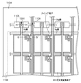
図1は、本発明の好適な実施の形態に係る放射線撮像装置の平面図である。図2は、図1に示す1画素の破線部A−A’の断面図である。図3は、図1に示すSig接続ホール103、Vs線及びSig線の交差部102の破線部B−B’の断面図である。なお、図1には3列×2行の画素が示されているが、画素数はこれに限定されない。
[第2の実施形態]
図4は、本発明の好適な実施の形態に係る放射線撮像装置の平面図である。図5は、図4に示す1画素の破線部C−C’の断面図である。図6は、図4に示すSig接続ホール403、Vs線及びSig線の交差部402の破線部D−D’の断面図である。なお、図4には3列×2行の画素が示されているが、画素数はこれに限定されない。
[第3の実施形態]
図7は、本発明の好適な実施の形態に係る放射線撮像装置の平面図である。図8は、図7に示す1画素の破線部E−E’の断面図である。図9は、図7に示すSig接続ホール702、Vs線及びSig線の交差部701の破線部F−F’の断面図である。なお、図1には3列×2行の画素が示されているが、画素数はこれに限定されない。
[応用例]
図10は、本発明の好適な実施の形態に係る放射線撮像装置を放射線診断システムへ適用した場合の応用例を示す図である。
1101 基板
1103 画素領域
Claims (13)
- 電極と半導体層と不純物半導体層とをこの順に含んで放射線を電荷に変換する変換素子と、前記変換素子の前記電極に電気的に接続されたスイッチ素子と、を含む画素がマトリクス状に配置された画素領域と、
前記スイッチ素子に電気的に接続され、前記変換素子の前記電極に所定の電圧を与えるための第1の電圧が与えられる第1の線と、
前記変換素子の前記不純物半導体層に電気的に接続され、前記所定の電圧との差により前記変換素子の前記半導体層を空乏化する第2の電圧が与えられる第2の線と、
前記画素領域の外で、前記第1の線と前記第2の線とが交差する交差部と、
を基板上に備える放射線撮像装置であって、
前記交差部では、前記第1の線と前記第2の線との間に半導体層が配置され、前記交差部の前記半導体層と前記第2の線との間に前記変換素子の前記不純物半導体層と同じ型の不純物半導体層が配置され、前記交差部の前記半導体層と前記第1の線との間にキャリア阻止部が配置されていることを特徴とする放射線撮像装置。 - 前記第1の線は、前記基板と前記第2の線との間に配置されていることを特徴とする請求項1に記載の放射線撮像装置。
- 前記変換素子の前記不純物半導体層及び前記交差部の前記不純物半導体層は、n型半導体層であることを特徴とする請求項1又は2に記載の放射線撮像装置。
- 前記変換素子で放射線を電荷に変換する際に、前記第1の線のフェルミ準位が前記第2の線のフェルミ準位よりも高くなるように構成されていることを特徴とする請求項3に記載の放射線撮像装置。
- 前記変換素子で放射線を電荷に変換する際に、前記第1の線に前記第1の電圧を与え、前記第2の線に前記第2の電圧を与えるよう構成され、前記第2の電圧が前記第1の電圧よりも高いことを特徴とする請求項4に記載の放射線撮像装置。
- 前記変換素子の前記不純物半導体層及び前記交差部の前記不純物半導体層は、p型半導体層であることを特徴とする請求項1又は2に記載の放射線撮像装置。
- 前記キャリア阻止部と前記交差部の前記半導体層との間にn型半導体層が配置されていることを特徴とする請求項6に記載の放射線撮像装置。
- 前記第2の線と前記交差部の前記半導体層との間に電極層が配置されていることを特徴とする請求項6又は7に記載の放射線撮像装置。
- 前記変換素子で放射線を電荷に変換する際に、前記第1の線のフェルミ準位が前記第2の線のフェルミ準位よりも低くなるように構成されていることを特徴とする請求項6乃至8のいずれか1項に記載の放射線撮像装置。
- 前記変換素子で放射線を電荷に変換する際に、前記第1の線に前記第1の電圧を与え、前記第2の線に前記第2の電圧を与えるよう構成され、前記第2の電圧が前記第1の電圧よりも低いことを特徴とする請求項9に記載の放射線撮像装置。
- 前記キャリア阻止部は、第1の絶縁層及び第2の絶縁層を含むことを特徴とする請求項1乃至10のいずれか1項に記載の放射線撮像装置。
- 前記交差部の前記半導体層は、アモルファスシリコンで形成されていることを特徴とする請求項1乃至11のいずれか1項に記載の放射線撮像装置。
- 請求項1乃至12のいずれか1項に記載の放射線撮像装置と、
前記放射線撮像装置からの信号を処理する信号処理手段と、
を備えることを特徴とする放射線撮像システム。
Priority Applications (4)
| Application Number | Priority Date | Filing Date | Title |
|---|---|---|---|
| JP2007099751A JP5173234B2 (ja) | 2006-05-24 | 2007-04-05 | 放射線撮像装置及び放射線撮像システム |
| US11/751,702 US7470908B2 (en) | 2006-05-24 | 2007-05-22 | Radiation imaging apparatus and radiation imaging system |
| US12/210,839 US7642517B2 (en) | 2006-05-24 | 2008-09-15 | Radiation imaging apparatus and radiation imaging system |
| US12/627,635 US8519344B2 (en) | 2006-05-24 | 2009-11-30 | Radiation imaging apparatus and radiation imaging system |
Applications Claiming Priority (3)
| Application Number | Priority Date | Filing Date | Title |
|---|---|---|---|
| JP2006144683 | 2006-05-24 | ||
| JP2006144683 | 2006-05-24 | ||
| JP2007099751A JP5173234B2 (ja) | 2006-05-24 | 2007-04-05 | 放射線撮像装置及び放射線撮像システム |
Publications (3)
| Publication Number | Publication Date |
|---|---|
| JP2008004920A JP2008004920A (ja) | 2008-01-10 |
| JP2008004920A5 JP2008004920A5 (ja) | 2010-05-20 |
| JP5173234B2 true JP5173234B2 (ja) | 2013-04-03 |
Family
ID=38748689
Family Applications (1)
| Application Number | Title | Priority Date | Filing Date |
|---|---|---|---|
| JP2007099751A Expired - Fee Related JP5173234B2 (ja) | 2006-05-24 | 2007-04-05 | 放射線撮像装置及び放射線撮像システム |
Country Status (2)
| Country | Link |
|---|---|
| US (3) | US7470908B2 (ja) |
| JP (1) | JP5173234B2 (ja) |
Families Citing this family (32)
| Publication number | Priority date | Publication date | Assignee | Title |
|---|---|---|---|---|
| JP5043374B2 (ja) * | 2005-07-11 | 2012-10-10 | キヤノン株式会社 | 変換装置、放射線検出装置、及び放射線検出システム |
| JP5043380B2 (ja) * | 2005-07-25 | 2012-10-10 | キヤノン株式会社 | 放射線検出装置および放射線検出システム |
| JP5159065B2 (ja) | 2005-08-31 | 2013-03-06 | キヤノン株式会社 | 放射線検出装置、放射線撮像装置および放射線撮像システム |
| JP2007201246A (ja) * | 2006-01-27 | 2007-08-09 | Canon Inc | 光電変換装置及び放射線撮像装置 |
| JP5196739B2 (ja) * | 2006-06-09 | 2013-05-15 | キヤノン株式会社 | 放射線撮像装置及び放射線撮像システム |
| JP5235350B2 (ja) * | 2007-08-07 | 2013-07-10 | キヤノン株式会社 | 撮像装置及び放射線撮像システム |
| KR101218089B1 (ko) * | 2007-12-07 | 2013-01-18 | 엘지디스플레이 주식회사 | 디지털 엑스레이 디텍터 및 그 제조방법 |
| JP5489542B2 (ja) * | 2008-07-01 | 2014-05-14 | キヤノン株式会社 | 放射線検出装置及び放射線撮像システム |
| JP2010210590A (ja) * | 2009-03-12 | 2010-09-24 | Fujifilm Corp | 放射線検出器 |
| JP5665494B2 (ja) * | 2010-06-24 | 2015-02-04 | キヤノン株式会社 | 放射線検出装置及び放射線撮像システム |
| JP2012182759A (ja) * | 2011-03-03 | 2012-09-20 | Konica Minolta Medical & Graphic Inc | 放射線検出パネルおよび放射線画像撮影装置 |
| JP5954983B2 (ja) | 2011-12-21 | 2016-07-20 | キヤノン株式会社 | 撮像装置及び放射線撮像システム、並びに撮像装置の製造方法 |
| JP6057511B2 (ja) | 2011-12-21 | 2017-01-11 | キヤノン株式会社 | 撮像装置及び放射線撮像システム |
| JP6463136B2 (ja) * | 2014-02-14 | 2019-01-30 | キヤノン株式会社 | 放射線検出装置及び放射線検出システム |
| JP6339853B2 (ja) | 2014-05-01 | 2018-06-06 | キヤノン株式会社 | 放射線撮像装置および放射線撮像システム |
| JP6585910B2 (ja) | 2014-05-01 | 2019-10-02 | キヤノン株式会社 | 放射線撮像装置および放射線撮像システム |
| JP6478538B2 (ja) | 2014-09-10 | 2019-03-06 | キヤノン株式会社 | 放射線撮像装置および放射線撮像システム |
| WO2016104339A1 (ja) * | 2014-12-25 | 2016-06-30 | シャープ株式会社 | フォトセンサ基板、及びその製造方法 |
| JP6570315B2 (ja) | 2015-05-22 | 2019-09-04 | キヤノン株式会社 | 放射線撮像装置及び放射線撮像システム |
| JP2017187546A (ja) * | 2016-04-01 | 2017-10-12 | 株式会社ジャパンディスプレイ | 表示装置 |
| JP6415488B2 (ja) | 2016-07-08 | 2018-10-31 | キヤノン株式会社 | 放射線撮像システム |
| JP6929104B2 (ja) | 2017-04-05 | 2021-09-01 | キヤノン株式会社 | 放射線撮像装置、放射線撮像システム、放射線撮像装置の制御方法及びプログラム |
| JP6990986B2 (ja) | 2017-04-27 | 2022-01-12 | キヤノン株式会社 | 放射線撮像装置、放射線撮像システム、放射線撮像装置の制御方法及びプログラム |
| JP6853729B2 (ja) | 2017-05-08 | 2021-03-31 | キヤノン株式会社 | 放射線撮像装置、放射線撮像システム、放射線撮像装置の制御方法及びプログラム |
| JP6788547B2 (ja) | 2017-05-09 | 2020-11-25 | キヤノン株式会社 | 放射線撮像装置、その制御方法、制御装置、及び、放射線撮像システム |
| JP6877289B2 (ja) | 2017-07-31 | 2021-05-26 | キヤノン株式会社 | 放射線検出装置、放射線検出システム、及び放射線出装置の製造方法 |
| JP7045834B2 (ja) | 2017-11-10 | 2022-04-01 | キヤノン株式会社 | 放射線撮像システム |
| JP7079113B2 (ja) | 2018-02-21 | 2022-06-01 | キヤノン株式会社 | 放射線撮像装置及び放射線撮像システム |
| JP7198003B2 (ja) | 2018-06-22 | 2022-12-28 | キヤノン株式会社 | 放射線撮像装置、放射線撮像システム、放射線撮像装置の制御方法およびプログラム |
| JP6659182B2 (ja) | 2018-07-23 | 2020-03-04 | キヤノン株式会社 | 放射線撮像装置、その製造方法及び放射線撮像システム |
| EP3661190A1 (en) | 2018-11-27 | 2020-06-03 | Canon Kabushiki Kaisha | Radiation imaging apparatus and radiation imaging system |
| JP7397635B2 (ja) | 2019-11-22 | 2023-12-13 | キヤノン株式会社 | 放射線検出装置、放射線検出システム、制御方法及びプログラム |
Family Cites Families (28)
| Publication number | Priority date | Publication date | Assignee | Title |
|---|---|---|---|---|
| JP3066944B2 (ja) * | 1993-12-27 | 2000-07-17 | キヤノン株式会社 | 光電変換装置、その駆動方法及びそれを有するシステム |
| US5648674A (en) * | 1995-06-07 | 1997-07-15 | Xerox Corporation | Array circuitry with conductive lines, contact leads, and storage capacitor electrode all formed in layer that includes highly conductive metal |
| JPH0998970A (ja) * | 1995-10-06 | 1997-04-15 | Canon Inc | X線撮像装置 |
| US6060173A (en) * | 1996-04-17 | 2000-05-09 | Englehard Corporation | Metal honeycomb body |
| JP2000512084A (ja) * | 1997-04-02 | 2000-09-12 | コーニンクレッカ フィリップス エレクトロニクス エヌ ヴィ | センサマトリックスを有するx線装置 |
| JP3636579B2 (ja) * | 1997-11-04 | 2005-04-06 | キヤノン株式会社 | 光電変換装置、光電変換装置の駆動方法及びその光電変換装置を有するシステム |
| US6060714A (en) * | 1998-01-23 | 2000-05-09 | Ois Optical Imaging Systems, Inc. | Large area imager with photo-imageable interface barrier layer |
| JP3916823B2 (ja) * | 1999-04-07 | 2007-05-23 | シャープ株式会社 | アクティブマトリクス基板およびその製造方法、並びにフラットパネル型イメージセンサ |
| JP5016746B2 (ja) * | 2000-07-28 | 2012-09-05 | キヤノン株式会社 | 撮像装置及びその駆動方法 |
| US7034309B2 (en) * | 2001-11-13 | 2006-04-25 | Canon Kabushiki Kaisha | Radiation detecting apparatus and method of driving the same |
| JP2003347534A (ja) * | 2002-05-28 | 2003-12-05 | Canon Inc | 放射線検出装置及びその製造方法 |
| US7214945B2 (en) * | 2002-06-11 | 2007-05-08 | Canon Kabushiki Kaisha | Radiation detecting apparatus, manufacturing method therefor, and radiation image pickup system |
| JP4018461B2 (ja) * | 2002-06-11 | 2007-12-05 | キヤノン株式会社 | 放射線検出装置及びその製造方法並びに放射線撮像システム |
| US7148487B2 (en) * | 2002-08-27 | 2006-12-12 | Canon Kabushiki Kaisha | Image sensing apparatus and method using radiation |
| JP4266656B2 (ja) * | 2003-02-14 | 2009-05-20 | キヤノン株式会社 | 固体撮像装置及び放射線撮像装置 |
| JP4323827B2 (ja) * | 2003-02-14 | 2009-09-02 | キヤノン株式会社 | 固体撮像装置及び放射線撮像装置 |
| US7541617B2 (en) * | 2003-02-14 | 2009-06-02 | Canon Kabushiki Kaisha | Radiation image pickup device |
| JP4217505B2 (ja) * | 2003-02-28 | 2009-02-04 | キヤノン株式会社 | 撮像装置及びx線撮像装置 |
| JP2004296654A (ja) * | 2003-03-26 | 2004-10-21 | Canon Inc | 放射線撮像装置 |
| JP4418720B2 (ja) * | 2003-11-21 | 2010-02-24 | キヤノン株式会社 | 放射線撮像装置及び方法、並びに放射線撮像システム |
| US7126128B2 (en) * | 2004-02-13 | 2006-10-24 | Kabushiki Kaisha Toshiba | Flat panel x-ray detector |
| US7403594B2 (en) * | 2004-03-31 | 2008-07-22 | Canon Kabushiki Kaisha | Radiation imaging apparatus and control method therefor |
| JP4845352B2 (ja) * | 2004-06-15 | 2011-12-28 | キヤノン株式会社 | 放射線撮像装置、その製造方法及び放射線撮像システム |
| US7557355B2 (en) * | 2004-09-30 | 2009-07-07 | Canon Kabushiki Kaisha | Image pickup apparatus and radiation image pickup apparatus |
| JP5043374B2 (ja) * | 2005-07-11 | 2012-10-10 | キヤノン株式会社 | 変換装置、放射線検出装置、及び放射線検出システム |
| JP5043373B2 (ja) * | 2005-07-11 | 2012-10-10 | キヤノン株式会社 | 変換装置、放射線検出装置、及び放射線検出システム |
| JP2007101256A (ja) * | 2005-09-30 | 2007-04-19 | Fujifilm Corp | X線撮像装置及びx線ct装置 |
| JP4847202B2 (ja) * | 2006-04-27 | 2011-12-28 | キヤノン株式会社 | 撮像装置及び放射線撮像システム |
-
2007
- 2007-04-05 JP JP2007099751A patent/JP5173234B2/ja not_active Expired - Fee Related
- 2007-05-22 US US11/751,702 patent/US7470908B2/en not_active Expired - Fee Related
-
2008
- 2008-09-15 US US12/210,839 patent/US7642517B2/en not_active Expired - Fee Related
-
2009
- 2009-11-30 US US12/627,635 patent/US8519344B2/en not_active Expired - Fee Related
Also Published As
| Publication number | Publication date |
|---|---|
| US20100072381A1 (en) | 2010-03-25 |
| US20070272870A1 (en) | 2007-11-29 |
| US20090008533A1 (en) | 2009-01-08 |
| US7642517B2 (en) | 2010-01-05 |
| US8519344B2 (en) | 2013-08-27 |
| US7470908B2 (en) | 2008-12-30 |
| JP2008004920A (ja) | 2008-01-10 |
Similar Documents
| Publication | Publication Date | Title |
|---|---|---|
| JP5173234B2 (ja) | 放射線撮像装置及び放射線撮像システム | |
| US7541617B2 (en) | Radiation image pickup device | |
| JP4307322B2 (ja) | 放射線撮像装置及び放射線撮像システム | |
| US7573041B2 (en) | Imaging apparatus, radiation imaging apparatus, and radiation imaging system | |
| US7030385B2 (en) | Radiation detecting apparatus and method of driving the same | |
| US9190437B2 (en) | Semiconductor detection apparatus capable of switching capacitance among different levels, and detection system including the apparatus | |
| JP5439984B2 (ja) | 光電変換装置および放射線撮像装置 | |
| JP5328169B2 (ja) | 撮像装置及び放射線撮像システム | |
| JP2004265934A (ja) | 固体撮像装置及び放射線撮像装置 | |
| JP2010034520A (ja) | 放射線検出装置及び放射線撮像システム | |
| JP2007329434A (ja) | 放射線撮像装置及び放射線撮像システム | |
| JP2005114731A (ja) | 後方照射を有する半導体放射線撮像装置 | |
| JP4067055B2 (ja) | 撮像装置及びその製造方法、放射線撮像装置、放射線撮像システム | |
| JP5974654B2 (ja) | 撮像装置および撮像表示システム | |
| US9564461B2 (en) | Radiation image-pickup device and radiation image-pickup display system | |
| JP2004296654A (ja) | 放射線撮像装置 | |
| JP4314255B2 (ja) | 変換装置およびx線検出システム | |
| JP2002124676A (ja) | 半導体装置 | |
| JP4393085B2 (ja) | 放射線検出装置 | |
| JP2004303925A (ja) | 撮像用基板 | |
| CN104425530A (zh) | 放射线摄像装置和放射线摄像显示系统 | |
| JP2016134386A (ja) | 光電変換素子及び撮像装置 | |
| JP2006186032A (ja) | 放射線撮像装置 |
Legal Events
| Date | Code | Title | Description |
|---|---|---|---|
| A521 | Request for written amendment filed |
Free format text: JAPANESE INTERMEDIATE CODE: A523 Effective date: 20100402 |
|
| A621 | Written request for application examination |
Free format text: JAPANESE INTERMEDIATE CODE: A621 Effective date: 20100402 |
|
| A977 | Report on retrieval |
Free format text: JAPANESE INTERMEDIATE CODE: A971007 Effective date: 20120831 |
|
| A131 | Notification of reasons for refusal |
Free format text: JAPANESE INTERMEDIATE CODE: A131 Effective date: 20120907 |
|
| A521 | Request for written amendment filed |
Free format text: JAPANESE INTERMEDIATE CODE: A523 Effective date: 20121026 |
|
| TRDD | Decision of grant or rejection written | ||
| A01 | Written decision to grant a patent or to grant a registration (utility model) |
Free format text: JAPANESE INTERMEDIATE CODE: A01 Effective date: 20121203 |
|
| A61 | First payment of annual fees (during grant procedure) |
Free format text: JAPANESE INTERMEDIATE CODE: A61 Effective date: 20121227 |
|
| FPAY | Renewal fee payment (event date is renewal date of database) |
Free format text: PAYMENT UNTIL: 20160111 Year of fee payment: 3 |
|
| LAPS | Cancellation because of no payment of annual fees |