JP5117740B2 - 半導体装置の製造方法 - Google Patents
半導体装置の製造方法 Download PDFInfo
- Publication number
- JP5117740B2 JP5117740B2 JP2007051060A JP2007051060A JP5117740B2 JP 5117740 B2 JP5117740 B2 JP 5117740B2 JP 2007051060 A JP2007051060 A JP 2007051060A JP 2007051060 A JP2007051060 A JP 2007051060A JP 5117740 B2 JP5117740 B2 JP 5117740B2
- Authority
- JP
- Japan
- Prior art keywords
- film
- polycrystalline
- silicon
- metal
- forming
- Prior art date
- Legal status (The legal status is an assumption and is not a legal conclusion. Google has not performed a legal analysis and makes no representation as to the accuracy of the status listed.)
- Expired - Fee Related
Links
Images


Classifications
-
- H—ELECTRICITY
- H01—ELECTRIC ELEMENTS
- H01L—SEMICONDUCTOR DEVICES NOT COVERED BY CLASS H10
- H01L21/00—Processes or apparatus adapted for the manufacture or treatment of semiconductor or solid state devices or of parts thereof
- H01L21/02—Manufacture or treatment of semiconductor devices or of parts thereof
- H01L21/04—Manufacture or treatment of semiconductor devices or of parts thereof the devices having potential barriers, e.g. a PN junction, depletion layer or carrier concentration layer
- H01L21/18—Manufacture or treatment of semiconductor devices or of parts thereof the devices having potential barriers, e.g. a PN junction, depletion layer or carrier concentration layer the devices having semiconductor bodies comprising elements of Group IV of the Periodic Table or AIIIBV compounds with or without impurities, e.g. doping materials
- H01L21/28—Manufacture of electrodes on semiconductor bodies using processes or apparatus not provided for in groups H01L21/20 - H01L21/268
- H01L21/28008—Making conductor-insulator-semiconductor electrodes
- H01L21/28017—Making conductor-insulator-semiconductor electrodes the insulator being formed after the semiconductor body, the semiconductor being silicon
- H01L21/28026—Making conductor-insulator-semiconductor electrodes the insulator being formed after the semiconductor body, the semiconductor being silicon characterised by the conductor
- H01L21/28097—Making conductor-insulator-semiconductor electrodes the insulator being formed after the semiconductor body, the semiconductor being silicon characterised by the conductor the final conductor layer next to the insulator being a metallic silicide
-
- H—ELECTRICITY
- H10—SEMICONDUCTOR DEVICES; ELECTRIC SOLID-STATE DEVICES NOT OTHERWISE PROVIDED FOR
- H10D—INORGANIC ELECTRIC SEMICONDUCTOR DEVICES
- H10D64/00—Electrodes of devices having potential barriers
- H10D64/01—Manufacture or treatment
- H10D64/017—Manufacture or treatment using dummy gates in processes wherein at least parts of the final gates are self-aligned to the dummy gates, i.e. replacement gate processes
-
- H—ELECTRICITY
- H10—SEMICONDUCTOR DEVICES; ELECTRIC SOLID-STATE DEVICES NOT OTHERWISE PROVIDED FOR
- H10D—INORGANIC ELECTRIC SEMICONDUCTOR DEVICES
- H10D84/00—Integrated devices formed in or on semiconductor substrates that comprise only semiconducting layers, e.g. on Si wafers or on GaAs-on-Si wafers
- H10D84/01—Manufacture or treatment
- H10D84/0123—Integrating together multiple components covered by H10D12/00 or H10D30/00, e.g. integrating multiple IGBTs
- H10D84/0126—Integrating together multiple components covered by H10D12/00 or H10D30/00, e.g. integrating multiple IGBTs the components including insulated gates, e.g. IGFETs
- H10D84/0165—Integrating together multiple components covered by H10D12/00 or H10D30/00, e.g. integrating multiple IGBTs the components including insulated gates, e.g. IGFETs the components including complementary IGFETs, e.g. CMOS devices
- H10D84/0172—Manufacturing their gate conductors
- H10D84/0174—Manufacturing their gate conductors the gate conductors being silicided
-
- H—ELECTRICITY
- H10—SEMICONDUCTOR DEVICES; ELECTRIC SOLID-STATE DEVICES NOT OTHERWISE PROVIDED FOR
- H10D—INORGANIC ELECTRIC SEMICONDUCTOR DEVICES
- H10D84/00—Integrated devices formed in or on semiconductor substrates that comprise only semiconducting layers, e.g. on Si wafers or on GaAs-on-Si wafers
- H10D84/01—Manufacture or treatment
- H10D84/0123—Integrating together multiple components covered by H10D12/00 or H10D30/00, e.g. integrating multiple IGBTs
- H10D84/0126—Integrating together multiple components covered by H10D12/00 or H10D30/00, e.g. integrating multiple IGBTs the components including insulated gates, e.g. IGFETs
- H10D84/0165—Integrating together multiple components covered by H10D12/00 or H10D30/00, e.g. integrating multiple IGBTs the components including insulated gates, e.g. IGFETs the components including complementary IGFETs, e.g. CMOS devices
- H10D84/0172—Manufacturing their gate conductors
- H10D84/0177—Manufacturing their gate conductors the gate conductors having different materials or different implants
-
- H—ELECTRICITY
- H10—SEMICONDUCTOR DEVICES; ELECTRIC SOLID-STATE DEVICES NOT OTHERWISE PROVIDED FOR
- H10D—INORGANIC ELECTRIC SEMICONDUCTOR DEVICES
- H10D84/00—Integrated devices formed in or on semiconductor substrates that comprise only semiconducting layers, e.g. on Si wafers or on GaAs-on-Si wafers
- H10D84/01—Manufacture or treatment
- H10D84/0123—Integrating together multiple components covered by H10D12/00 or H10D30/00, e.g. integrating multiple IGBTs
- H10D84/0126—Integrating together multiple components covered by H10D12/00 or H10D30/00, e.g. integrating multiple IGBTs the components including insulated gates, e.g. IGFETs
- H10D84/0165—Integrating together multiple components covered by H10D12/00 or H10D30/00, e.g. integrating multiple IGBTs the components including insulated gates, e.g. IGFETs the components including complementary IGFETs, e.g. CMOS devices
- H10D84/0172—Manufacturing their gate conductors
- H10D84/0179—Manufacturing their gate conductors the gate conductors having different shapes or dimensions
-
- H—ELECTRICITY
- H10—SEMICONDUCTOR DEVICES; ELECTRIC SOLID-STATE DEVICES NOT OTHERWISE PROVIDED FOR
- H10D—INORGANIC ELECTRIC SEMICONDUCTOR DEVICES
- H10D84/00—Integrated devices formed in or on semiconductor substrates that comprise only semiconducting layers, e.g. on Si wafers or on GaAs-on-Si wafers
- H10D84/01—Manufacture or treatment
- H10D84/02—Manufacture or treatment characterised by using material-based technologies
- H10D84/03—Manufacture or treatment characterised by using material-based technologies using Group IV technology, e.g. silicon technology or silicon-carbide [SiC] technology
- H10D84/038—Manufacture or treatment characterised by using material-based technologies using Group IV technology, e.g. silicon technology or silicon-carbide [SiC] technology using silicon technology, e.g. SiGe
-
- H—ELECTRICITY
- H01—ELECTRIC ELEMENTS
- H01L—SEMICONDUCTOR DEVICES NOT COVERED BY CLASS H10
- H01L2924/00—Indexing scheme for arrangements or methods for connecting or disconnecting semiconductor or solid-state bodies as covered by H01L24/00
- H01L2924/0001—Technical content checked by a classifier
- H01L2924/0002—Not covered by any one of groups H01L24/00, H01L24/00 and H01L2224/00
-
- H—ELECTRICITY
- H10—SEMICONDUCTOR DEVICES; ELECTRIC SOLID-STATE DEVICES NOT OTHERWISE PROVIDED FOR
- H10D—INORGANIC ELECTRIC SEMICONDUCTOR DEVICES
- H10D30/00—Field-effect transistors [FET]
- H10D30/01—Manufacture or treatment
- H10D30/021—Manufacture or treatment of FETs having insulated gates [IGFET]
- H10D30/0212—Manufacture or treatment of FETs having insulated gates [IGFET] using self-aligned silicidation
-
- H—ELECTRICITY
- H10—SEMICONDUCTOR DEVICES; ELECTRIC SOLID-STATE DEVICES NOT OTHERWISE PROVIDED FOR
- H10D—INORGANIC ELECTRIC SEMICONDUCTOR DEVICES
- H10D64/00—Electrodes of devices having potential barriers
- H10D64/60—Electrodes characterised by their materials
- H10D64/66—Electrodes having a conductor capacitively coupled to a semiconductor by an insulator, e.g. MIS electrodes
- H10D64/667—Electrodes having a conductor capacitively coupled to a semiconductor by an insulator, e.g. MIS electrodes the conductor comprising a layer of alloy material, compound material or organic material contacting the insulator, e.g. TiN workfunction layers
- H10D64/668—Electrodes having a conductor capacitively coupled to a semiconductor by an insulator, e.g. MIS electrodes the conductor comprising a layer of alloy material, compound material or organic material contacting the insulator, e.g. TiN workfunction layers the layer being a silicide, e.g. TiSi2
Landscapes
- Engineering & Computer Science (AREA)
- Physics & Mathematics (AREA)
- Condensed Matter Physics & Semiconductors (AREA)
- General Physics & Mathematics (AREA)
- Manufacturing & Machinery (AREA)
- Computer Hardware Design (AREA)
- Microelectronics & Electronic Packaging (AREA)
- Power Engineering (AREA)
- Electrodes Of Semiconductors (AREA)
- Metal-Oxide And Bipolar Metal-Oxide Semiconductor Integrated Circuits (AREA)
- Insulated Gate Type Field-Effect Transistor (AREA)
Description
前記素子分離膜によって分割形成された複数の能動素子領域表面に不純物を導入する工程と、
前記能動素子領域にゲート絶縁膜を形成する工程と、
前記ゲート絶縁膜上に多結晶膜を成膜し、選択的にエッチングして複数のゲート電極を形成する工程と
前記多結晶膜を挟んで、ソース・ドレイン領域を形成する工程と、
前記ソース・ドレイン領域表面に選択的に、前記多結晶膜を構成する元素と同種の元素を必須として含む金属半導体化合物からなる導電膜を形成する工程と、
前記多結晶膜と前記導電膜とを覆う層間絶縁膜を形成する工程と、
前記層間絶縁膜を選択的に除去して前記多結晶膜上面を露出させる工程と、
前記露出した多結晶膜上面に金属膜を成膜する工程と、
加熱して前記多結晶膜と前記金属膜とを反応させ、前記金属膜を構成する金属と多結晶膜を構成する元素とを必須として含む金属半導体化合物からなるゲート電極を複数形成する工程と、
前記複数のゲート電極のうち一部のゲート電極上に選択的に前記多結晶膜を構成する元素と同種の元素膜を配置する工程と、
加熱して前記ゲート電極と選択的に配置された前記元素膜とを反応させ、前記金属の組成比が前記反応前の組成比よりも減少されたゲート電極を形成する工程と、
未反応の前記元素膜を選択的に除去する工程と、
を含み、
前記多結晶膜を構成する元素がシリコンおよび/またはゲルマニウムである、半導体装置の製造方法が提供される。
前記層間絶縁膜を選択的に除去して前記多結晶膜上面を露出させる工程の後、前記露出した多結晶膜上面に金属膜を成膜する工程の前に、少なくとも1以上の前記多結晶膜の厚みを選択的に低減させて、異なる厚みの多結晶膜を形成する工程をさらに含む、半導体装置の製造方法が提供される。
半導体装置において、同一組成成分で異なる組成比のゲート電極を含むトランジスタを複数含む構成とすることで、複数の閾値電圧を設定することができる。
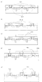
図1は、本実施形態にかかるMISFETの断面図である。図中、半導体基板上に、素子分離絶縁膜により分離された3つのMISFETが配置されている。チャネル領域の不純物濃度は同一であり、また、ゲート絶縁膜も同一である。ゲート電極は、金属組成比の異なる金属シリサイド、金属ジャーマナイド、または金属シリコン・ジャーマナイドであり、同一基板不純物濃度領域101上に形成される。金属シリサイドの場合、例えばそれぞれ、NiSi、Ni2Si、Ni3Siである。
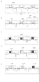
図2を用いて、本発明の第2の実施形態を説明する。便宜上、ここでは可能な限り、ひとつのトランジスタの断面図で説明し、必要に応じて複数のトランジスタの断面図を使用する。
実施形態3として、図3を用いて、NiSi、Ni2Si、Ni3Siの3つのシリサイドゲート電極を形成する方法を説明する。
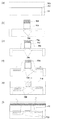
上記に説明した実施形態では、Ni2Si、NiSiに変化させたゲート電極はその上面位置が上昇する。そのため、ゲート電極形成後の第2の層間絶縁膜形成後の表面には、その高さの変化分だけ段差が形成される。次に、このような段差の生じない、本発明の実施形態4について図4を用いて説明する。
さらに、上記の実施形態においてゲート電極にシリコンを用いたが、シリコンの代わりにゲルマニウムまたはシリコン・ゲルマニウムを用いてもよい。例えば、ゲルマニウム基板を用いてゲート絶縁膜上にゲルマニウム膜を形成することでゲート電極およびソース・ドレイン領域を金属ジャーマナイドにすることができる。
201 同一基板不純物濃度領域
202 シリコン多結晶膜
203 シリコン膜
204 未反応のシリコン膜
301 同一基板不純物濃度領域
302 シリコン多結晶膜
303 シリコン膜
304 未反応のシリコン膜
305 シリコン膜
401 同一基板不純物濃度領域
402 シリコン多結晶膜
403 犠牲ゲート電極
404 マスク
501 シリコン基板
502 ソース・ドレイン・エクステンション
503 不純物高濃度領域
504 金属シリサイド膜
505 ゲート絶縁膜
506 金属シリサイド
507 側壁スペーサシリコン窒化膜
601 シリコン基板
602 犠牲ゲート
603 側壁シリコン酸化膜
604 ソース・ドレイン・エクステンション
605 シリコン窒化膜スペーサ
606 不純物高濃度領域
701 シリコン基板
702 ゲート絶縁膜
703 シリコン多結晶膜
704 ハードマスク
705 犠牲ゲート
706 ソース・ドレイン・エクステンション
707 側壁シリコン酸化膜
708 シリコン窒化膜スペーサ
709 不純物高濃度領域
710 層間絶縁膜
801 短い犠牲ゲート
802 長い犠牲ゲート
803 Ni過剰シリサイド
804 未反応犠牲ゲート
901 短い犠牲ゲート
902 長い犠牲ゲート
903 シリコン多結晶膜
Claims (3)
- 半導体基板上に素子分離膜を形成する工程と、
前記素子分離膜によって分割形成された複数の能動素子領域表面に不純物を導入する工程と、
前記能動素子領域にゲート絶縁膜を形成する工程と、
前記ゲート絶縁膜上に多結晶膜を成膜し、選択的にエッチングして複数のゲート電極を形成する工程と、
前記多結晶膜を挟んで、ソース・ドレイン領域を形成する工程と、
前記ソース・ドレイン領域表面に選択的に、前記多結晶膜を構成する元素と同種の元素を必須として含む金属半導体化合物からなる導電膜を形成する工程と、
前記多結晶膜と前記導電膜とを覆う層間絶縁膜を形成する工程と、
前記層間絶縁膜を選択的に除去して前記多結晶膜上面を露出させる工程と、
前記露出した多結晶膜上面に金属膜を成膜する工程と、
加熱して前記多結晶膜と前記金属膜とを反応させ、前記金属膜を構成する金属と多結晶膜を構成する元素とを必須として含む金属半導体化合物からなるゲート電極を複数形成する工程と、
前記複数のゲート電極のうち一部のゲート電極上に選択的に前記多結晶膜を構成する元素と同種の元素膜を配置する工程と、
加熱して前記ゲート電極と選択的に配置された前記元素膜とを反応させ、前記金属の組成比が前記反応前の組成比よりも減少されたゲート電極を形成する工程と、
未反応の前記元素膜を選択的に除去する工程と、
を含み、
前記多結晶膜を構成する元素がシリコンおよび/またはゲルマニウムである、半導体装置の製造方法。 - 請求項1に記載の半導体装置の製造方法において、
前記層間絶縁膜を選択的に除去して前記多結晶膜上面を露出させる工程の後、前記露出した多結晶膜上面に金属膜を成膜する工程の前に、少なくとも1以上の前記多結晶膜の厚みを選択的に低減させて、異なる厚みの多結晶膜を形成する工程をさらに含む、半導体装置の製造方法。 - 前記多結晶膜を構成する元素がシリコンである、請求項1または2に記載の半導体装置の製造方法。
Priority Applications (3)
| Application Number | Priority Date | Filing Date | Title |
|---|---|---|---|
| JP2007051060A JP5117740B2 (ja) | 2007-03-01 | 2007-03-01 | 半導体装置の製造方法 |
| US12/068,713 US7816213B2 (en) | 2007-03-01 | 2008-02-11 | Semiconductor device having transistors each having gate electrode of different metal ratio and production process thereof |
| US12/923,747 US8299536B2 (en) | 2007-03-01 | 2010-10-06 | Semiconductor device having transistors each having gate electrode of different metal ratio and production process thereof |
Applications Claiming Priority (1)
| Application Number | Priority Date | Filing Date | Title |
|---|---|---|---|
| JP2007051060A JP5117740B2 (ja) | 2007-03-01 | 2007-03-01 | 半導体装置の製造方法 |
Publications (2)
| Publication Number | Publication Date |
|---|---|
| JP2008218544A JP2008218544A (ja) | 2008-09-18 |
| JP5117740B2 true JP5117740B2 (ja) | 2013-01-16 |
Family
ID=39732453
Family Applications (1)
| Application Number | Title | Priority Date | Filing Date |
|---|---|---|---|
| JP2007051060A Expired - Fee Related JP5117740B2 (ja) | 2007-03-01 | 2007-03-01 | 半導体装置の製造方法 |
Country Status (2)
| Country | Link |
|---|---|
| US (2) | US7816213B2 (ja) |
| JP (1) | JP5117740B2 (ja) |
Families Citing this family (8)
| Publication number | Priority date | Publication date | Assignee | Title |
|---|---|---|---|---|
| JP5117740B2 (ja) * | 2007-03-01 | 2013-01-16 | ルネサスエレクトロニクス株式会社 | 半導体装置の製造方法 |
| US7906351B2 (en) * | 2008-08-07 | 2011-03-15 | Texas Instruments Incorporated | Method for metal gate quality characterization |
| US8012817B2 (en) * | 2008-09-26 | 2011-09-06 | Taiwan Semiconductor Manufacturing Company, Ltd. | Transistor performance improving method with metal gate |
| US8703594B2 (en) | 2011-10-25 | 2014-04-22 | Taiwan Semiconductor Manufacturing Company, Ltd. | Semiconductor device having a treated gate structure and fabrication method thereof |
| JP6149634B2 (ja) * | 2013-09-17 | 2017-06-21 | 富士通セミコンダクター株式会社 | 半導体装置及びその製造方法 |
| US10546856B2 (en) | 2014-02-25 | 2020-01-28 | Stmicroelectronics, Inc. | CMOS structure having low resistance contacts and fabrication method |
| US10032635B2 (en) * | 2015-02-05 | 2018-07-24 | The Trustees Of The University Of Pennsylvania | Thin film metal silicides and methods for formation |
| US10332809B1 (en) * | 2018-06-21 | 2019-06-25 | International Business Machines Corporation | Method and structure to introduce strain in stack nanosheet field effect transistor |
Family Cites Families (52)
| Publication number | Priority date | Publication date | Assignee | Title |
|---|---|---|---|---|
| JPH077826B2 (ja) * | 1983-08-25 | 1995-01-30 | 忠弘 大見 | 半導体集積回路 |
| US5256591A (en) * | 1991-01-07 | 1993-10-26 | Gold Star Electron Co., Ltd. | Method for forming isolation region in semiconductor device using trench |
| US5576579A (en) * | 1995-01-12 | 1996-11-19 | International Business Machines Corporation | Tasin oxygen diffusion barrier in multilayer structures |
| JPH10189483A (ja) * | 1996-12-26 | 1998-07-21 | Fujitsu Ltd | 半導体装置の製造方法及び半導体装置 |
| US6406743B1 (en) * | 1997-07-10 | 2002-06-18 | Industrial Technology Research Institute | Nickel-silicide formation by electroless Ni deposition on polysilicon |
| JP3090198B2 (ja) * | 1997-08-21 | 2000-09-18 | 日本電気株式会社 | 半導体装置の構造およびその製造方法 |
| KR100319681B1 (ko) * | 1998-12-02 | 2002-01-09 | 가네꼬 히사시 | 전계 효과 트랜지스터 및 그 제조 방법 |
| JP3287403B2 (ja) | 1999-02-19 | 2002-06-04 | 日本電気株式会社 | Mis型電界効果トランジスタ及びその製造方法 |
| JP2000243958A (ja) * | 1999-02-24 | 2000-09-08 | Toshiba Corp | 半導体装置およびその製造方法 |
| JP3175725B2 (ja) * | 1999-02-24 | 2001-06-11 | 日本電気株式会社 | 半導体装置の製造方法 |
| JP3379464B2 (ja) * | 1999-02-26 | 2003-02-24 | 日本電気株式会社 | 半導体装置の製造方法及びスパッタリング装置 |
| JP2000252462A (ja) | 1999-03-01 | 2000-09-14 | Toshiba Corp | Mis型半導体装置及びその製造方法 |
| JP3211809B2 (ja) * | 1999-04-23 | 2001-09-25 | ソニー株式会社 | 半導体記憶装置およびその製造方法 |
| JP4237332B2 (ja) * | 1999-04-30 | 2009-03-11 | 株式会社東芝 | 半導体装置の製造方法 |
| US6274488B1 (en) * | 2000-04-12 | 2001-08-14 | Ultratech Stepper, Inc. | Method of forming a silicide region in a Si substrate and a device having same |
| US6420264B1 (en) * | 2000-04-12 | 2002-07-16 | Ultratech Stepper, Inc. | Method of forming a silicide region in a Si substrate and a device having same |
| JP4776755B2 (ja) * | 2000-06-08 | 2011-09-21 | ルネサスエレクトロニクス株式会社 | 半導体装置およびその製造方法 |
| JP2002217313A (ja) * | 2000-11-30 | 2002-08-02 | Texas Instruments Inc | 金属及び対応する金属珪化物から形成した各ゲートを有する相補形トランジスタ |
| US6605513B2 (en) * | 2000-12-06 | 2003-08-12 | Advanced Micro Devices, Inc. | Method of forming nickel silicide using a one-step rapid thermal anneal process and backend processing |
| US6380057B1 (en) * | 2001-02-13 | 2002-04-30 | Advanced Micro Devices, Inc. | Enhancement of nickel silicide formation by use of nickel pre-amorphizing implant |
| US6432805B1 (en) * | 2001-02-15 | 2002-08-13 | Advanced Micro Devices, Inc. | Co-deposition of nitrogen and metal for metal silicide formation |
| US6645798B2 (en) * | 2001-06-22 | 2003-11-11 | Micron Technology, Inc. | Metal gate engineering for surface p-channel devices |
| SG107563A1 (en) * | 2001-07-31 | 2004-12-29 | Agency Science Tech & Res | Gate electrodes and the formation thereof |
| US6770521B2 (en) * | 2001-11-30 | 2004-08-03 | Texas Instruments Incorporated | Method of making multiple work function gates by implanting metals with metallic alloying additives |
| US6982474B2 (en) * | 2002-06-25 | 2006-01-03 | Amberwave Systems Corporation | Reacted conductive gate electrodes |
| US6723658B2 (en) * | 2002-07-15 | 2004-04-20 | Texas Instruments Incorporated | Gate structure and method |
| US6936528B2 (en) * | 2002-10-17 | 2005-08-30 | Samsung Electronics Co., Ltd. | Method of forming cobalt silicide film and method of manufacturing semiconductor device having cobalt silicide film |
| JP2005047753A (ja) * | 2003-07-29 | 2005-02-24 | Tadahiro Omi | 炭化珪素製品、その製造方法、及び、炭化珪素製品の洗浄方法 |
| JP4011024B2 (ja) | 2004-01-30 | 2007-11-21 | 株式会社ルネサステクノロジ | 半導体装置およびその製造方法 |
| JP4457688B2 (ja) | 2004-02-12 | 2010-04-28 | ソニー株式会社 | 半導体装置 |
| JP4623006B2 (ja) * | 2004-06-23 | 2011-02-02 | 日本電気株式会社 | 半導体装置及びその製造方法 |
| JP2006041339A (ja) * | 2004-07-29 | 2006-02-09 | Fujitsu Ltd | Cmos集積回路 |
| JP4116990B2 (ja) * | 2004-09-28 | 2008-07-09 | 富士通株式会社 | 電界効果型トランジスタおよびその製造方法 |
| JP2006108355A (ja) * | 2004-10-05 | 2006-04-20 | Renesas Technology Corp | 半導体装置およびその製造方法 |
| JP2006269673A (ja) * | 2005-03-23 | 2006-10-05 | Nec Electronics Corp | 半導体装置およびその製造方法 |
| JP2006278369A (ja) * | 2005-03-28 | 2006-10-12 | Fujitsu Ltd | 半導体装置の製造方法 |
| JP5015446B2 (ja) * | 2005-05-16 | 2012-08-29 | アイメック | 二重の完全ケイ化ゲートを形成する方法と前記方法によって得られたデバイス |
| JP2006344836A (ja) * | 2005-06-09 | 2006-12-21 | Matsushita Electric Ind Co Ltd | 半導体装置及びその製造方法 |
| WO2006137371A1 (ja) * | 2005-06-23 | 2006-12-28 | Nec Corporation | 半導体装置 |
| US7151023B1 (en) * | 2005-08-01 | 2006-12-19 | International Business Machines Corporation | Metal gate MOSFET by full semiconductor metal alloy conversion |
| JP5157450B2 (ja) * | 2005-11-28 | 2013-03-06 | 日本電気株式会社 | 半導体装置およびその製造方法 |
| JP4309911B2 (ja) * | 2006-06-08 | 2009-08-05 | 株式会社東芝 | 半導体装置およびその製造方法 |
| US7605045B2 (en) * | 2006-07-13 | 2009-10-20 | Advanced Micro Devices, Inc. | Field effect transistors and methods for fabricating the same |
| JP2008117963A (ja) * | 2006-11-06 | 2008-05-22 | Nec Electronics Corp | 電界効果トランジスタおよび半導体装置、ならびにそれらの製造方法 |
| JP2008131023A (ja) * | 2006-11-27 | 2008-06-05 | Nec Electronics Corp | 半導体装置およびその製造方法 |
| JP5117740B2 (ja) * | 2007-03-01 | 2013-01-16 | ルネサスエレクトロニクス株式会社 | 半導体装置の製造方法 |
| JP5222583B2 (ja) * | 2007-04-06 | 2013-06-26 | パナソニック株式会社 | 半導体装置 |
| TW200910526A (en) * | 2007-07-03 | 2009-03-01 | Renesas Tech Corp | Method of manufacturing semiconductor device |
| JP2009059882A (ja) * | 2007-08-31 | 2009-03-19 | Nec Electronics Corp | 半導体装置 |
| US7642153B2 (en) * | 2007-10-23 | 2010-01-05 | Texas Instruments Incorporated | Methods for forming gate electrodes for integrated circuits |
| JP5430904B2 (ja) * | 2008-10-15 | 2014-03-05 | ルネサスエレクトロニクス株式会社 | 半導体装置の製造方法 |
| JP2011151134A (ja) * | 2010-01-20 | 2011-08-04 | Renesas Electronics Corp | 半導体装置、および、半導体装置の製造方法 |
-
2007
- 2007-03-01 JP JP2007051060A patent/JP5117740B2/ja not_active Expired - Fee Related
-
2008
- 2008-02-11 US US12/068,713 patent/US7816213B2/en not_active Expired - Fee Related
-
2010
- 2010-10-06 US US12/923,747 patent/US8299536B2/en not_active Expired - Fee Related
Also Published As
| Publication number | Publication date |
|---|---|
| US7816213B2 (en) | 2010-10-19 |
| JP2008218544A (ja) | 2008-09-18 |
| US20110031553A1 (en) | 2011-02-10 |
| US20080211000A1 (en) | 2008-09-04 |
| US8299536B2 (en) | 2012-10-30 |
Similar Documents
| Publication | Publication Date | Title |
|---|---|---|
| CN112201626B (zh) | 半导体装置 | |
| US8836038B2 (en) | CMOS dual metal gate semiconductor device | |
| US20090227079A1 (en) | Semiconductor device and manufacturing method thereof | |
| CN101069282B (zh) | 用于在cmos器件中形成自对准双重全硅化栅极的方法 | |
| CN101233611A (zh) | 通过全半导体金属合金转变的金属栅极mosfet | |
| JP5117740B2 (ja) | 半導体装置の製造方法 | |
| US20060170047A1 (en) | Semiconductor device and method of manufacturing the same | |
| US20090302390A1 (en) | Method of manufacturing semiconductor device with different metallic gates | |
| JP4920310B2 (ja) | 半導体装置およびその製造方法 | |
| JP2009043938A (ja) | 半導体装置および半導体装置の製造方法 | |
| JP2006278369A (ja) | 半導体装置の製造方法 | |
| JP2006196646A (ja) | 半導体装置及びその製造方法 | |
| JP2008103644A (ja) | 半導体装置およびその製造方法 | |
| JP2007158220A (ja) | 半導体装置の製造方法 | |
| JP2008277420A (ja) | 半導体装置およびその製造方法 | |
| JP2008243942A (ja) | 半導体装置の製造方法及び半導体装置 | |
| JP4401358B2 (ja) | 半導体装置の製造方法 | |
| JP2008047586A (ja) | 半導体装置およびその製造方法 | |
| JP2007180390A (ja) | 半導体装置およびその製造方法 | |
| JP4957040B2 (ja) | 半導体装置、および半導体装置の製造方法。 | |
| JP2009170762A (ja) | 半導体装置および半導体装置の製造方法 | |
| JP2009117402A (ja) | 半導体装置の製造方法 | |
| JP2007180354A (ja) | 半導体装置及びその製造方法 | |
| JP2007266293A (ja) | 半導体装置、および半導体装置の製造方法。 |
Legal Events
| Date | Code | Title | Description |
|---|---|---|---|
| A621 | Written request for application examination |
Free format text: JAPANESE INTERMEDIATE CODE: A621 Effective date: 20100215 |
|
| A977 | Report on retrieval |
Free format text: JAPANESE INTERMEDIATE CODE: A971007 Effective date: 20120704 |
|
| A131 | Notification of reasons for refusal |
Free format text: JAPANESE INTERMEDIATE CODE: A131 Effective date: 20120710 |
|
| A521 | Request for written amendment filed |
Free format text: JAPANESE INTERMEDIATE CODE: A523 Effective date: 20120910 |
|
| TRDD | Decision of grant or rejection written | ||
| A01 | Written decision to grant a patent or to grant a registration (utility model) |
Free format text: JAPANESE INTERMEDIATE CODE: A01 Effective date: 20121016 |
|
| A01 | Written decision to grant a patent or to grant a registration (utility model) |
Free format text: JAPANESE INTERMEDIATE CODE: A01 |
|
| A61 | First payment of annual fees (during grant procedure) |
Free format text: JAPANESE INTERMEDIATE CODE: A61 Effective date: 20121018 |
|
| R150 | Certificate of patent or registration of utility model |
Free format text: JAPANESE INTERMEDIATE CODE: R150 |
|
| FPAY | Renewal fee payment (event date is renewal date of database) |
Free format text: PAYMENT UNTIL: 20151026 Year of fee payment: 3 |
|
| S531 | Written request for registration of change of domicile |
Free format text: JAPANESE INTERMEDIATE CODE: R313531 |
|
| R350 | Written notification of registration of transfer |
Free format text: JAPANESE INTERMEDIATE CODE: R350 |
|
| LAPS | Cancellation because of no payment of annual fees |