JP5087540B2 - 窒化物半導体発光素子 - Google Patents
窒化物半導体発光素子 Download PDFInfo
- Publication number
- JP5087540B2 JP5087540B2 JP2008517721A JP2008517721A JP5087540B2 JP 5087540 B2 JP5087540 B2 JP 5087540B2 JP 2008517721 A JP2008517721 A JP 2008517721A JP 2008517721 A JP2008517721 A JP 2008517721A JP 5087540 B2 JP5087540 B2 JP 5087540B2
- Authority
- JP
- Japan
- Prior art keywords
- layer
- nitride semiconductor
- type
- emitting device
- semiconductor light
- Prior art date
- Legal status (The legal status is an assumption and is not a legal conclusion. Google has not performed a legal analysis and makes no representation as to the accuracy of the status listed.)
- Expired - Fee Related
Links
Images


Classifications
-
- H—ELECTRICITY
- H01—ELECTRIC ELEMENTS
- H01L—SEMICONDUCTOR DEVICES NOT COVERED BY CLASS H10
- H01L33/00—Semiconductor devices with at least one potential-jump barrier or surface barrier specially adapted for light emission; Processes or apparatus specially adapted for the manufacture or treatment thereof or of parts thereof; Details thereof
- H01L33/02—Semiconductor devices with at least one potential-jump barrier or surface barrier specially adapted for light emission; Processes or apparatus specially adapted for the manufacture or treatment thereof or of parts thereof; Details thereof characterised by the semiconductor bodies
- H01L33/04—Semiconductor devices with at least one potential-jump barrier or surface barrier specially adapted for light emission; Processes or apparatus specially adapted for the manufacture or treatment thereof or of parts thereof; Details thereof characterised by the semiconductor bodies with a quantum effect structure or superlattice, e.g. tunnel junction
-
- H—ELECTRICITY
- H01—ELECTRIC ELEMENTS
- H01L—SEMICONDUCTOR DEVICES NOT COVERED BY CLASS H10
- H01L33/00—Semiconductor devices with at least one potential-jump barrier or surface barrier specially adapted for light emission; Processes or apparatus specially adapted for the manufacture or treatment thereof or of parts thereof; Details thereof
- H01L33/02—Semiconductor devices with at least one potential-jump barrier or surface barrier specially adapted for light emission; Processes or apparatus specially adapted for the manufacture or treatment thereof or of parts thereof; Details thereof characterised by the semiconductor bodies
- H01L33/26—Materials of the light emitting region
- H01L33/30—Materials of the light emitting region containing only elements of group III and group V of the periodic system
- H01L33/32—Materials of the light emitting region containing only elements of group III and group V of the periodic system containing nitrogen
-
- H—ELECTRICITY
- H01—ELECTRIC ELEMENTS
- H01L—SEMICONDUCTOR DEVICES NOT COVERED BY CLASS H10
- H01L33/00—Semiconductor devices with at least one potential-jump barrier or surface barrier specially adapted for light emission; Processes or apparatus specially adapted for the manufacture or treatment thereof or of parts thereof; Details thereof
- H01L33/02—Semiconductor devices with at least one potential-jump barrier or surface barrier specially adapted for light emission; Processes or apparatus specially adapted for the manufacture or treatment thereof or of parts thereof; Details thereof characterised by the semiconductor bodies
- H01L33/04—Semiconductor devices with at least one potential-jump barrier or surface barrier specially adapted for light emission; Processes or apparatus specially adapted for the manufacture or treatment thereof or of parts thereof; Details thereof characterised by the semiconductor bodies with a quantum effect structure or superlattice, e.g. tunnel junction
- H01L33/06—Semiconductor devices with at least one potential-jump barrier or surface barrier specially adapted for light emission; Processes or apparatus specially adapted for the manufacture or treatment thereof or of parts thereof; Details thereof characterised by the semiconductor bodies with a quantum effect structure or superlattice, e.g. tunnel junction within the light emitting region, e.g. quantum confinement structure or tunnel barrier
Description
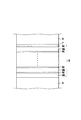
2 バッファ層
3 アンドープGaN層
4 n型GaNコンタクト層
5 InGaN/GaN超格子層
6 活性層
6a 障壁層
6b 障壁層
6c 井戸層
7 アンドープInGaN層
8 p型GaN系コンタクト層
9 p電極
10 n電極
11 p型AlGaNクラッド層
Claims (11)
- Inを含む窒化物からなる井戸層と窒化物からなる第1の障壁層とで構成された量子井戸構造を有する活性層をp型窒化物半導体層とn型窒化物半導体層とで挟む構造を備えた窒化物半導体発光素子において、
前記活性層のp側に最も近い位置に配置された井戸層と前記p型窒化物半導体層との間に形成された中間半導体層は、アンドープInGaN層と前記活性層の窒化物からなる第2の障壁層との積層体で構成され、前記アンドープInGaN層は、In組成が前記p型窒化物半導体層に向かって減少していくIn組成傾斜層であり、前記アンドープInGaN層と前記第2の障壁層が接する地点の前記アンドープInGaN層のバンドギャップは、前記第2の障壁層のバンドギャップに等しく形成されるとともに、前記中間半導体層の膜厚は20nm以下であることを特徴とする窒化物半導体発光素子。 - 前記第2の障壁層は、前記第1の障壁層よりも薄く形成されていることを特徴とする請求項1に記載の窒化物半導体発光素子。
- 前記第1の障壁層の膜厚は100Å〜350Åであり、前記第2の障壁層の膜厚は20Å〜30Åであることを特徴とする請求項2に記載の窒化物半導体発光素子。
- 前記第2の障壁層は、InXGa1−XN層(0≦X<1)で構成されていることを特徴とする請求項1〜請求項3のいずれか1項に記載の窒化物半導体発光素子。
- 前記第2の障壁層は、InXGa1−XN層(0<X<1)で構成され、In組成は0.5%〜1%の範囲であることを特徴とする請求項1〜請求項3のいずれか1項に記載の窒化物半導体発光素子。
- 前記In組成傾斜層のIn傾斜は前記p型窒化物半導体層を形成する成長温度に達するまでの温度上昇過程によって形成されることを特徴とする請求項5記載の窒化物半導体発光素子。
- 前記p型窒化物半導体層の一部としてp電極と接触するp型コンタクト層が形成されており、前記p型コンタクト層はMgドープInGaN又はMgドープGaNで構成されていることを特徴とする請求項1〜請求項6のいずれか1項に記載の窒化物半導体発光素子。
- 前記アンドープInGaN層とp型コンタクト層との間には、前記p型窒化物半導体層の一部としてMgがドープされたp型AlxGaN(0.02≦x≦0.15)が形成されていることを特徴とする請求項7に記載の窒化物半導体発光素子。
- 前記p型AlxGaN(0.02≦x≦0.15)のホールキャリア濃度は、2×1017cm−3以上の範囲であることを特徴とする請求項8に記載の窒化物半導体発光素子。
- 前記p型AlxGaN(0.02≦x≦0.15)は、温度1000℃以上で成長させることを特徴とする請求項8又は請求項9のいずれか1項に記載の窒化物半導体発光素子。
- 前記井戸層のIn組成比率は10%以上であって、前記活性層のp側に最も近い位置に配置された井戸層成膜終了から前記p型窒化物半導体層の成膜終了までの間に、成長温度が950℃以上となる時間の合計が30分以内であることを特徴とする請求項1〜請求項10のいずれか1項に記載の窒化物半導体発光素子。
Applications Claiming Priority (1)
| Application Number | Priority Date | Filing Date | Title |
|---|---|---|---|
| PCT/JP2006/310546 WO2007138657A1 (ja) | 2006-05-26 | 2006-05-26 | 窒化物半導体発光素子 |
Publications (2)
| Publication Number | Publication Date |
|---|---|
| JPWO2007138657A1 JPWO2007138657A1 (ja) | 2009-10-01 |
| JP5087540B2 true JP5087540B2 (ja) | 2012-12-05 |
Family
ID=38778186
Family Applications (1)
| Application Number | Title | Priority Date | Filing Date |
|---|---|---|---|
| JP2008517721A Expired - Fee Related JP5087540B2 (ja) | 2006-05-26 | 2006-05-26 | 窒化物半導体発光素子 |
Country Status (5)
| Country | Link |
|---|---|
| US (1) | US20100065812A1 (ja) |
| EP (1) | EP2034525A1 (ja) |
| JP (1) | JP5087540B2 (ja) |
| CN (1) | CN101449394A (ja) |
| WO (1) | WO2007138657A1 (ja) |
Families Citing this family (16)
| Publication number | Priority date | Publication date | Assignee | Title |
|---|---|---|---|---|
| JP2008235606A (ja) * | 2007-03-20 | 2008-10-02 | Sony Corp | 半導体発光素子、半導体発光素子の製造方法、バックライト、表示装置、電子機器および発光装置 |
| US7928448B2 (en) | 2007-12-04 | 2011-04-19 | Philips Lumileds Lighting Company, Llc | III-nitride light emitting device including porous semiconductor layer |
| KR101549811B1 (ko) * | 2009-01-09 | 2015-09-04 | 삼성전자주식회사 | 질화물 반도체 발광소자 |
| US8586963B2 (en) | 2009-12-08 | 2013-11-19 | Lehigh University | Semiconductor light-emitting devices having concave microstructures providing improved light extraction efficiency and method for producing same |
| US8525148B2 (en) * | 2010-07-16 | 2013-09-03 | Micron Technology, Inc. | Solid state lighting devices without converter materials and associated methods of manufacturing |
| FR3003397B1 (fr) | 2013-03-15 | 2016-07-22 | Soitec Silicon On Insulator | Structures semi-conductrices dotées de régions actives comprenant de l'INGAN |
| FR3004585B1 (fr) * | 2013-04-12 | 2017-12-29 | Soitec Silicon On Insulator | Structures semi-conductrices dotees de regions actives comprenant de l'ingan |
| DE112014001423T5 (de) * | 2013-03-15 | 2015-12-24 | Soitec | Halbleiterstrukturen mit InGaN umfassenden Aktivbereichen, Verfahren zum Bilden derartiger Halbleiterstrukturen und aus derartigen Halbleiterstrukturen gebildete Licht emittierende Vorrichtungen |
| TWI593135B (zh) | 2013-03-15 | 2017-07-21 | 索泰克公司 | 具有含氮化銦鎵之主動區域之半導體結構,形成此等半導體結構之方法,以及應用此等半導體結構形成之發光元件 |
| US9343626B2 (en) | 2013-03-15 | 2016-05-17 | Soitec | Semiconductor structures having active regions comprising InGaN, methods of forming such semiconductor structures, and light emitting devices formed from such semiconductor structures |
| CN104701432A (zh) * | 2015-03-20 | 2015-06-10 | 映瑞光电科技(上海)有限公司 | GaN 基LED 外延结构及其制备方法 |
| JP2016195166A (ja) * | 2015-03-31 | 2016-11-17 | ウシオ電機株式会社 | 半導体発光素子及びその製造方法 |
| CN105428448B (zh) * | 2015-09-29 | 2018-06-08 | 北京大学 | 一种双组分渐变结构太阳能电池及其制备方法 |
| JP6669095B2 (ja) * | 2017-02-06 | 2020-03-18 | 日亜化学工業株式会社 | 窒化物半導体発光素子の製造方法 |
| CN113097359B (zh) * | 2021-03-29 | 2022-08-26 | 厦门士兰明镓化合物半导体有限公司 | 半导体发光元件 |
| CN113964246A (zh) * | 2021-09-28 | 2022-01-21 | 厦门士兰明镓化合物半导体有限公司 | 发光二极管的外延结构及其制造方法 |
Citations (5)
| Publication number | Priority date | Publication date | Assignee | Title |
|---|---|---|---|---|
| JP2000286448A (ja) * | 1999-03-31 | 2000-10-13 | Toyoda Gosei Co Ltd | Iii族窒化物系化合物半導体発光素子 |
| JP2001077413A (ja) * | 1999-09-06 | 2001-03-23 | Showa Denko Kk | Iii族窒化物半導体発光素子およびその製造方法 |
| JP2004134772A (ja) * | 2002-09-18 | 2004-04-30 | Sanyo Electric Co Ltd | 窒化物系半導体発光素子 |
| JP2005012216A (ja) * | 2003-06-18 | 2005-01-13 | Lumileds Lighting Us Llc | Iii族窒化物発光デバイスのためのヘテロ構造 |
| JP2006005331A (ja) * | 2004-05-18 | 2006-01-05 | Sumitomo Electric Ind Ltd | Iii族窒化物半導体結晶およびその製造方法、iii族窒化物半導体デバイスおよびその製造方法ならびに発光機器 |
Family Cites Families (6)
| Publication number | Priority date | Publication date | Assignee | Title |
|---|---|---|---|---|
| JP3679914B2 (ja) * | 1997-02-12 | 2005-08-03 | 株式会社東芝 | 半導体発光装置及びその製造方法 |
| JP3420028B2 (ja) * | 1997-07-29 | 2003-06-23 | 株式会社東芝 | GaN系化合物半導体素子の製造方法 |
| JP3864735B2 (ja) * | 2000-12-28 | 2007-01-10 | ソニー株式会社 | 半導体発光素子およびその製造方法 |
| JP4388720B2 (ja) * | 2001-10-12 | 2009-12-24 | 住友電気工業株式会社 | 半導体発光素子の製造方法 |
| US7485902B2 (en) * | 2002-09-18 | 2009-02-03 | Sanyo Electric Co., Ltd. | Nitride-based semiconductor light-emitting device |
| JP2006108585A (ja) * | 2004-10-08 | 2006-04-20 | Toyoda Gosei Co Ltd | Iii族窒化物系化合物半導体発光素子 |
-
2006
- 2006-05-26 CN CNA2006800547286A patent/CN101449394A/zh active Pending
- 2006-05-26 WO PCT/JP2006/310546 patent/WO2007138657A1/ja active Application Filing
- 2006-05-26 US US12/227,693 patent/US20100065812A1/en not_active Abandoned
- 2006-05-26 EP EP06756646A patent/EP2034525A1/en not_active Withdrawn
- 2006-05-26 JP JP2008517721A patent/JP5087540B2/ja not_active Expired - Fee Related
Patent Citations (5)
| Publication number | Priority date | Publication date | Assignee | Title |
|---|---|---|---|---|
| JP2000286448A (ja) * | 1999-03-31 | 2000-10-13 | Toyoda Gosei Co Ltd | Iii族窒化物系化合物半導体発光素子 |
| JP2001077413A (ja) * | 1999-09-06 | 2001-03-23 | Showa Denko Kk | Iii族窒化物半導体発光素子およびその製造方法 |
| JP2004134772A (ja) * | 2002-09-18 | 2004-04-30 | Sanyo Electric Co Ltd | 窒化物系半導体発光素子 |
| JP2005012216A (ja) * | 2003-06-18 | 2005-01-13 | Lumileds Lighting Us Llc | Iii族窒化物発光デバイスのためのヘテロ構造 |
| JP2006005331A (ja) * | 2004-05-18 | 2006-01-05 | Sumitomo Electric Ind Ltd | Iii族窒化物半導体結晶およびその製造方法、iii族窒化物半導体デバイスおよびその製造方法ならびに発光機器 |
Also Published As
| Publication number | Publication date |
|---|---|
| JPWO2007138657A1 (ja) | 2009-10-01 |
| WO2007138657A1 (ja) | 2007-12-06 |
| CN101449394A (zh) | 2009-06-03 |
| EP2034525A1 (en) | 2009-03-11 |
| US20100065812A1 (en) | 2010-03-18 |
Similar Documents
| Publication | Publication Date | Title |
|---|---|---|
| JP5087540B2 (ja) | 窒化物半導体発光素子 | |
| US8053756B2 (en) | Nitride semiconductor light emitting element | |
| JPWO2007138656A1 (ja) | 窒化物半導体発光素子 | |
| CN104576712B (zh) | 半导体装置及其制造方法 | |
| JP2003229645A (ja) | 量子井戸構造およびそれを用いた半導体素子ならびに半導体素子の製造方法 | |
| JP2008109092A (ja) | 半導体発光素子 | |
| JPH0715041A (ja) | 窒化ガリウム系化合物半導体発光素子 | |
| KR101213860B1 (ko) | 질화물계 반도체 발광 소자 | |
| KR102092517B1 (ko) | 질화물 반도체 자외선 발광 소자의 제조 방법 및 질화물 반도체 자외선 발광 소자 | |
| JP3763701B2 (ja) | 窒化ガリウム系半導体発光素子 | |
| KR20090026299A (ko) | 질화물 반도체 발광 소자 | |
| KR20090021177A (ko) | 질화물 반도체 발광 소자 | |
| KR20090021182A (ko) | 질화물 반도체 발광 소자 | |
| JP5733295B2 (ja) | 窒化物半導体発光素子、窒化物半導体発光素子を作製する方法 | |
| KR101373804B1 (ko) | 백색 발광다이오드 및 그 제조방법 | |
| JP2000261099A (ja) | Iii族窒化物レーザーダイオードおよびその製造方法 | |
| JP2007250878A (ja) | 半導体光デバイス | |
| Yasan et al. | Growth of deep-UV light-emitting diodes by metalorganic chemical vapor deposition | |
| JP2005252309A (ja) | 窒化ガリウム系半導体発光素子の製造方法 | |
| JP2019021852A (ja) | 紫外線発光素子 | |
| JP2004072044A (ja) | GaN系半導体発光素子の製造方法 | |
| JP2000216433A (ja) | 半導体素子、半導体発光素子およびn型半導体の形成方法 |
Legal Events
| Date | Code | Title | Description |
|---|---|---|---|
| A131 | Notification of reasons for refusal |
Free format text: JAPANESE INTERMEDIATE CODE: A131 Effective date: 20120221 |
|
| A521 | Request for written amendment filed |
Free format text: JAPANESE INTERMEDIATE CODE: A523 Effective date: 20120423 |
|
| A131 | Notification of reasons for refusal |
Free format text: JAPANESE INTERMEDIATE CODE: A131 Effective date: 20120612 |
|
| A521 | Request for written amendment filed |
Free format text: JAPANESE INTERMEDIATE CODE: A523 Effective date: 20120813 |
|
| TRDD | Decision of grant or rejection written | ||
| A01 | Written decision to grant a patent or to grant a registration (utility model) |
Free format text: JAPANESE INTERMEDIATE CODE: A01 Effective date: 20120904 |
|
| A01 | Written decision to grant a patent or to grant a registration (utility model) |
Free format text: JAPANESE INTERMEDIATE CODE: A01 |
|
| A61 | First payment of annual fees (during grant procedure) |
Free format text: JAPANESE INTERMEDIATE CODE: A61 Effective date: 20120910 |
|
| R150 | Certificate of patent or registration of utility model |
Ref document number: 5087540 Country of ref document: JP Free format text: JAPANESE INTERMEDIATE CODE: R150 Free format text: JAPANESE INTERMEDIATE CODE: R150 |
|
| FPAY | Renewal fee payment (event date is renewal date of database) |
Free format text: PAYMENT UNTIL: 20150914 Year of fee payment: 3 |
|
| LAPS | Cancellation because of no payment of annual fees |