JP4852234B2 - ボイド発生が防止される金属配線構造及び金属配線方法 - Google Patents
ボイド発生が防止される金属配線構造及び金属配線方法 Download PDFInfo
- Publication number
- JP4852234B2 JP4852234B2 JP2004222508A JP2004222508A JP4852234B2 JP 4852234 B2 JP4852234 B2 JP 4852234B2 JP 2004222508 A JP2004222508 A JP 2004222508A JP 2004222508 A JP2004222508 A JP 2004222508A JP 4852234 B2 JP4852234 B2 JP 4852234B2
- Authority
- JP
- Japan
- Prior art keywords
- metal wiring
- film
- trench
- via contact
- insulating film
- Prior art date
- Legal status (The legal status is an assumption and is not a legal conclusion. Google has not performed a legal analysis and makes no representation as to the accuracy of the status listed.)
- Expired - Fee Related
Links
Images


Classifications
-
- H—ELECTRICITY
- H10—SEMICONDUCTOR DEVICES; ELECTRIC SOLID-STATE DEVICES NOT OTHERWISE PROVIDED FOR
- H10D—INORGANIC ELECTRIC SEMICONDUCTOR DEVICES
- H10D64/00—Electrodes of devices having potential barriers
- H10D64/01—Manufacture or treatment
- H10D64/011—Manufacture or treatment of electrodes ohmically coupled to a semiconductor
-
- H—ELECTRICITY
- H10—SEMICONDUCTOR DEVICES; ELECTRIC SOLID-STATE DEVICES NOT OTHERWISE PROVIDED FOR
- H10W—GENERIC PACKAGES, INTERCONNECTIONS, CONNECTORS OR OTHER CONSTRUCTIONAL DETAILS OF DEVICES COVERED BY CLASS H10
- H10W20/00—Interconnections in chips, wafers or substrates
- H10W20/01—Manufacture or treatment
- H10W20/031—Manufacture or treatment of conductive parts of the interconnections
- H10W20/056—Manufacture or treatment of conductive parts of the interconnections by filling conductive material into holes, grooves or trenches
-
- H—ELECTRICITY
- H10—SEMICONDUCTOR DEVICES; ELECTRIC SOLID-STATE DEVICES NOT OTHERWISE PROVIDED FOR
- H10W—GENERIC PACKAGES, INTERCONNECTIONS, CONNECTORS OR OTHER CONSTRUCTIONAL DETAILS OF DEVICES COVERED BY CLASS H10
- H10W20/00—Interconnections in chips, wafers or substrates
- H10W20/01—Manufacture or treatment
- H10W20/031—Manufacture or treatment of conductive parts of the interconnections
- H10W20/032—Manufacture or treatment of conductive parts of the interconnections of conductive barrier, adhesion or liner layers
- H10W20/033—Manufacture or treatment of conductive parts of the interconnections of conductive barrier, adhesion or liner layers in openings in dielectrics
- H10W20/036—Manufacture or treatment of conductive parts of the interconnections of conductive barrier, adhesion or liner layers in openings in dielectrics the barrier, adhesion or liner layers being within a main fill metal
Landscapes
- Internal Circuitry In Semiconductor Integrated Circuit Devices (AREA)
Description
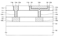
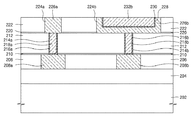
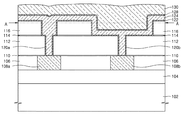
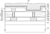
104、204 絶縁膜、
106、206 第1層間絶縁膜、
108a、208a 第1下部金属配線膜パターン、
108b、208b 第2下部金属配線膜パターン、
110、210 第1エッチング停止膜、
112、212 金属間絶縁膜、
114、220 第2エッチング停止膜、
116、222 第2層間絶縁膜、
118a、224a 第1トレンチ、
118b、224b 第2トレンチ、
120a、214a 第1ビアコンタクトホール、
120b、214b 第2ビアコンタクトホール、
122a、216a 第1障壁金属層、
122b、216b 第2障壁金属層、
124a、226a 第1上部金属配線膜パターン、
124b、226b 第2上部金属配線膜パターン、
128、230 ボイド拡散防止膜、
130b、232b 第3上部金属配線膜パターン、
218a 第1ビアコンタクト、
218b 第2ビアコンタクト、
228 第3トレンチ。
Claims (4)
- 第1層間絶縁膜内に配された下部金属配線膜パターンと、
前記第1層間絶縁膜及び下部金属膜パターン上で前記下部金属膜パターンの一部表面を露出させるビアコンタクトホールを有する金属間絶縁膜と、
前記ビアコンタクトホール内部面及び前記下部金属配線膜パターンの露出表面上に形成された障壁金属層と、
前記障壁金属層上で前記ビアコンタクトホール内部を充填するビアコンタクトと、
前記金属間絶縁膜及びビアコンタクト上で前記金属間絶縁膜の一部表面及びビアコンタクトの上部表面を露出させるトレンチを有する第2層間絶縁膜と、
前記金属間絶縁膜及び前記ビアコンタクト上で前記トレンチの底面および側面を被覆する、第1厚さの第1上部金属配線膜パターンと、
前記第1上部金属配線膜パターン上に形成されたボイド拡散防止膜と、
前記ボイド拡散防止膜上で前記トレンチ内部を全て充填する第2厚さの第2上部金属配線膜パターンとを備え、
前記第1上部金属配線膜パターンと第2上部金属配線膜パターンとは、同一の金属から形成され、
前記第1上部金属配線膜パターンの側壁は、前記第2層間絶縁膜と接することを特徴とする金属配線構造。 - 前記第2上部金属配線膜パターンの第2厚さは前記第1上部金属配線膜パターンの第1厚さの5倍以上であることを特徴とする請求項1に記載の金属配線構造。
- 第1層間絶縁膜内で相互離隔された第1領域及び第2領域にそれぞれ配される第1及び第2下部金属配線膜パターンと、
前記第1層間絶縁膜と前記第1及び第2下部金属配線膜パターン上に形成され、前記第1下部金属配線膜パターンの一部表面を露出させる第1ビアコンタクトホール及び前記第2下部金属配線膜パターンの一部表面を露出させる第2ビアコンタクトホールを含む、ビアコンタクトホールのみを有する金属間絶縁膜と、
前記第1ビアコンタクトホール及び第2ビアコンタクトホール内にそれぞれ形成された第1及び第2障壁金属層と、
前記第1及び第2障壁金属層上でそれぞれ第1及び第2ビアコンタクトホールを充填するように形成された第1及び第2ビアコンタクトと、
前記金属間絶縁膜上に形成され、前記第1ビアコンタクトの上部面を露出させる第1トレンチ及び前記第2ビアコンタクトの上部面を露出させる第2トレンチを有する第2層間絶縁膜と、
前記第1トレンチを充填するように形成された第1上部金属配線膜パターンと、
前記第2トレンチの底面および側面を被覆するように前記第2障壁金属層上に形成されることによって、前記第2トレンチ内の第3トレンチを形成させる第2上部金属配線膜パターンと、
前記第2上部金属配線膜パターン上に形成されたボイド拡散防止層と、
前記ボイド拡散防止層上で前記第3トレンチを充填する第3上部金属配線膜パターンとを含むことを特徴とする金属配線膜構造。
- 第1層間絶縁膜内に相互離隔された第1及び第2下部金属配線膜パターンを形成する段階と、
前記第1層間絶縁膜と前記第1及び第2下部金属配線膜パターン上に金属間絶縁膜を形成する段階と、
前記金属間絶縁膜の一部を除去し、前記第1及び第2下部金属配線膜パターンの一部表面をそれぞれ露出させる第1コンタクトホール及び第2コンタクトホールを形成する段階と、
前記金属間絶縁膜と前記第1及び第2下部金属配線膜パターンの露出表面上に障壁金属層を形成する段階と、
前記第1コンタクトホール及び第2コンタクトホールが充填されるように前記障壁金属層上に金属膜を形成する段階と、
平坦化を行い、前記金属膜を前記第1コンタクトホール内の第1ビアコンタクト及び前記第2コンタクトホール内の第2ビアコンタクトに分離させる段階と、
前記金属間絶縁膜、第1ビアコンタクト及び第2ビアコンタクト上に第2層間絶縁膜を形成する段階と、
前記第2層間絶縁膜の一部を除去し、前記第1ビアコンタクト及び第2ビアコンタクトの上部面をそれぞれ露出させる第1トレンチ及び第2トレンチを形成する段階と、
前記第1トレンチが充填されるように第1上部金属配線膜を形成し、前記第2トレンチ内部底面および側面を被覆するように前記障壁金属層上に第2上部金属配線膜を形成することにより、第3トレンチを形成させる段階と、
前記第3トレンチを有する第1上部金属配線膜上にボイド拡散防止層を形成する段階と、
前記第3トレンチが充填されるように前記ボイド拡散防止層上に第2上部金属配線膜を形成する段階と、
平坦化を行い、前記第1トレンチ内の第1上部金属配線膜と前記第2及び第3トレンチ内の第2及び第3上部金属配線膜とを分離させる段階とを含むことを特徴とする金属配線方法。
Applications Claiming Priority (2)
| Application Number | Priority Date | Filing Date | Title |
|---|---|---|---|
| KR1020030053890A KR100555513B1 (ko) | 2003-08-04 | 2003-08-04 | 보이드 발생이 방지되는 금속배선구조 및 금속배선방법 |
| KR2003-053890 | 2003-08-04 |
Publications (2)
| Publication Number | Publication Date |
|---|---|
| JP2005057277A JP2005057277A (ja) | 2005-03-03 |
| JP4852234B2 true JP4852234B2 (ja) | 2012-01-11 |
Family
ID=34114250
Family Applications (1)
| Application Number | Title | Priority Date | Filing Date |
|---|---|---|---|
| JP2004222508A Expired - Fee Related JP4852234B2 (ja) | 2003-08-04 | 2004-07-29 | ボイド発生が防止される金属配線構造及び金属配線方法 |
Country Status (4)
| Country | Link |
|---|---|
| US (1) | US6953745B2 (ja) |
| JP (1) | JP4852234B2 (ja) |
| KR (1) | KR100555513B1 (ja) |
| CN (1) | CN100392853C (ja) |
Families Citing this family (28)
| Publication number | Priority date | Publication date | Assignee | Title |
|---|---|---|---|---|
| TWI229411B (en) * | 2004-04-20 | 2005-03-11 | Powerchip Semiconductor Corp | Method of manufacturing a semiconductor device |
| US20060128147A1 (en) * | 2004-12-09 | 2006-06-15 | Honeywell International Inc. | Method of fabricating electrically conducting vias in a silicon wafer |
| JP2007081130A (ja) * | 2005-09-14 | 2007-03-29 | Toshiba Corp | 半導体装置の製造方法 |
| US8368220B2 (en) * | 2005-10-18 | 2013-02-05 | Taiwan Semiconductor Manufacturing Co. Ltd. | Anchored damascene structures |
| KR100660325B1 (ko) * | 2005-11-15 | 2006-12-22 | 동부일렉트로닉스 주식회사 | 반도체 소자의 제조방법 |
| US7514354B2 (en) | 2005-12-30 | 2009-04-07 | Samsung Electronics Co., Ltd | Methods for forming damascene wiring structures having line and plug conductors formed from different materials |
| KR100928507B1 (ko) * | 2007-12-03 | 2009-11-26 | 주식회사 동부하이텍 | 반도체 소자의 제조 방법 |
| JP2009278000A (ja) * | 2008-05-16 | 2009-11-26 | Toshiba Corp | 半導体装置及び半導体装置の製造方法 |
| KR101030663B1 (ko) * | 2008-06-27 | 2011-04-20 | 주식회사 하이닉스반도체 | 반도체 소자의 금속 배선 형성 방법 |
| JP2010171170A (ja) * | 2009-01-22 | 2010-08-05 | Hitachi Cable Ltd | 銅回路配線基板およびその製造方法 |
| TWI392405B (zh) * | 2009-10-26 | 2013-04-01 | Unimicron Technology Corp | 線路結構 |
| KR101300587B1 (ko) * | 2009-12-09 | 2013-08-28 | 한국전자통신연구원 | 반도체 소자의 제조 방법 |
| US8304863B2 (en) * | 2010-02-09 | 2012-11-06 | International Business Machines Corporation | Electromigration immune through-substrate vias |
| CN102196673B (zh) * | 2010-03-05 | 2013-10-16 | 欣兴电子股份有限公司 | 线路结构的制作方法 |
| KR101697573B1 (ko) * | 2010-11-29 | 2017-01-19 | 삼성전자 주식회사 | 반도체 장치, 그 제조 방법, 및 상기 반도체 장치를 포함하는 반도체 패키지 |
| CN102420171A (zh) * | 2011-05-13 | 2012-04-18 | 上海华力微电子有限公司 | 用于超厚顶层金属的双大马士革制造工艺 |
| US9269612B2 (en) * | 2011-11-22 | 2016-02-23 | Taiwan Semiconductor Manufacturing Company, Ltd. | Mechanisms of forming damascene interconnect structures |
| US8710660B2 (en) * | 2012-07-20 | 2014-04-29 | Taiwan Semiconductor Manufacturing Company, Ltd. | Hybrid interconnect scheme including aluminum metal line in low-k dielectric |
| US8772934B2 (en) * | 2012-08-28 | 2014-07-08 | Taiwan Semiconductor Manufacturing Company, Ltd. | Aluminum interconnection apparatus |
| US9252110B2 (en) * | 2014-01-17 | 2016-02-02 | Taiwan Semiconductor Manufacturing Company, Ltd. | Interconnect structure and method of forming same |
| US9530737B1 (en) * | 2015-09-28 | 2016-12-27 | Taiwan Semiconductor Manufacturing Co., Ltd. | Semiconductor device and manufacturing method thereof |
| US9824970B1 (en) * | 2016-06-27 | 2017-11-21 | Globalfoundries Inc. | Methods that use at least a dual damascene process and, optionally, a single damascene process to form interconnects with hybrid metallization and the resulting structures |
| CN110137153B (zh) * | 2018-02-09 | 2021-03-30 | 联华电子股份有限公司 | 半导体装置及其形成方法 |
| US10811353B2 (en) * | 2018-10-22 | 2020-10-20 | International Business Machines Corporation | Sub-ground rule e-Fuse structure |
| US10734338B2 (en) * | 2018-11-23 | 2020-08-04 | Nanya Technology Corporation | Bonding pad, semiconductor structure, and method of manufacturing semiconductor structure |
| KR102675935B1 (ko) * | 2019-12-16 | 2024-06-18 | 삼성전자주식회사 | 반도체 소자 |
| CN114126225B (zh) * | 2020-08-31 | 2024-12-17 | 庆鼎精密电子(淮安)有限公司 | 电路基板的制造方法、电路板及其制造方法 |
| US11488905B2 (en) * | 2020-12-08 | 2022-11-01 | Nanya Technology Corporation | Semiconductor device structure with manganese-containing conductive plug and method for forming the same |
Family Cites Families (20)
| Publication number | Priority date | Publication date | Assignee | Title |
|---|---|---|---|---|
| JP3391933B2 (ja) * | 1995-04-27 | 2003-03-31 | 沖電気工業株式会社 | 半導体素子とその製造方法 |
| US6174810B1 (en) * | 1998-04-06 | 2001-01-16 | Motorola, Inc. | Copper interconnect structure and method of formation |
| US6214696B1 (en) * | 1998-04-22 | 2001-04-10 | Texas Instruments - Acer Incorporated | Method of fabricating deep-shallow trench isolation |
| JP2943805B1 (ja) * | 1998-09-17 | 1999-08-30 | 日本電気株式会社 | 半導体装置及びその製造方法 |
| JP4044236B2 (ja) * | 1999-03-11 | 2008-02-06 | 株式会社東芝 | 半導体装置の製造方法 |
| US6144099A (en) * | 1999-03-30 | 2000-11-07 | Advanced Micro Devices, Inc. | Semiconductor metalization barrier |
| JP3365495B2 (ja) * | 1999-06-30 | 2003-01-14 | 日本電気株式会社 | 半導体装置およびその製造方法 |
| JP2001110809A (ja) * | 1999-10-04 | 2001-04-20 | Toshiba Corp | 半導体装置 |
| US6184128B1 (en) * | 2000-01-31 | 2001-02-06 | Advanced Micro Devices, Inc. | Method using a thin resist mask for dual damascene stop layer etch |
| JP2002050688A (ja) * | 2000-08-03 | 2002-02-15 | Seiko Epson Corp | 半導体装置およびその製造方法 |
| KR20020053610A (ko) | 2000-12-27 | 2002-07-05 | 박종섭 | 반도체장치의 배선 및 배선연결부 제조방법 |
| US6713874B1 (en) * | 2001-03-27 | 2004-03-30 | Advanced Micro Devices, Inc. | Semiconductor devices with dual nature capping/arc layers on organic-doped silica glass inter-layer dielectrics |
| US6486059B2 (en) * | 2001-04-19 | 2002-11-26 | Silicon Intergrated Systems Corp. | Dual damascene process using an oxide liner for a dielectric barrier layer |
| JP2003031574A (ja) * | 2001-07-13 | 2003-01-31 | Toshiba Corp | 半導体装置およびその製造方法 |
| JP3540302B2 (ja) * | 2001-10-19 | 2004-07-07 | Necエレクトロニクス株式会社 | 半導体装置およびその製造方法 |
| JP3886779B2 (ja) * | 2001-11-02 | 2007-02-28 | 富士通株式会社 | 絶縁膜形成用材料及び絶縁膜の形成方法 |
| JP2003218201A (ja) * | 2002-01-24 | 2003-07-31 | Mitsubishi Electric Corp | 半導体装置およびその製造方法 |
| JP2003282703A (ja) * | 2002-03-26 | 2003-10-03 | Hitachi Ltd | 半導体装置の製造方法および半導体装置 |
| JP4272168B2 (ja) * | 2003-03-28 | 2009-06-03 | 富士通マイクロエレクトロニクス株式会社 | 半導体装置及び半導体集積回路装置 |
| JP2004311865A (ja) * | 2003-04-10 | 2004-11-04 | Renesas Technology Corp | 配線構造 |
-
2003
- 2003-08-04 KR KR1020030053890A patent/KR100555513B1/ko not_active Expired - Fee Related
-
2004
- 2004-07-15 US US10/891,062 patent/US6953745B2/en not_active Expired - Lifetime
- 2004-07-29 JP JP2004222508A patent/JP4852234B2/ja not_active Expired - Fee Related
- 2004-08-04 CN CNB2004100558141A patent/CN100392853C/zh not_active Expired - Lifetime
Also Published As
| Publication number | Publication date |
|---|---|
| CN1581476A (zh) | 2005-02-16 |
| CN100392853C (zh) | 2008-06-04 |
| JP2005057277A (ja) | 2005-03-03 |
| US6953745B2 (en) | 2005-10-11 |
| US20050029010A1 (en) | 2005-02-10 |
| KR100555513B1 (ko) | 2006-03-03 |
| KR20050015190A (ko) | 2005-02-21 |
Similar Documents
| Publication | Publication Date | Title |
|---|---|---|
| JP4852234B2 (ja) | ボイド発生が防止される金属配線構造及び金属配線方法 | |
| JP3887282B2 (ja) | 金属−絶縁体−金属キャパシタ及びダマシン配線構造を有する半導体素子の製造方法 | |
| US6251740B1 (en) | Method of forming and electrically connecting a vertical interdigitated metal-insulator-metal capacitor extending between interconnect layers in an integrated circuit | |
| KR100413828B1 (ko) | 반도체 장치 및 그 형성방법 | |
| US6417535B1 (en) | Vertical interdigitated metal-insulator-metal capacitor for an integrated circuit | |
| US7709905B2 (en) | Dual damascene wiring and method | |
| US7214594B2 (en) | Method of making semiconductor device using a novel interconnect cladding layer | |
| JP7492618B2 (ja) | 二重金属電力レールを有する集積回路の製造方法 | |
| US6806579B2 (en) | Robust via structure and method | |
| KR20030035909A (ko) | 반도체장치 및 그 제조방법 | |
| US7932187B2 (en) | Method for fabricating a semiconductor device | |
| JP4338614B2 (ja) | 半導体装置およびその製造方法 | |
| USRE43320E1 (en) | Semiconductor device and manufacturing method thereof | |
| CN101471285A (zh) | 半导体器件及其制造方法 | |
| JP2005311123A (ja) | 半導体装置及びその製造方法 | |
| US20040192008A1 (en) | Semiconductor device including interconnection and capacitor, and method of manufacturing the same | |
| KR100763760B1 (ko) | 반도체 소자 제조 방법 | |
| JP4110829B2 (ja) | 半導体装置の製造方法 | |
| US6841471B2 (en) | Fabrication method of semiconductor device | |
| US7112537B2 (en) | Method of fabricating interconnection structure of semiconductor device | |
| KR100440472B1 (ko) | 반도체 소자 제조 방법 | |
| US6642139B1 (en) | Method for forming interconnection structure in an integration circuit | |
| JP2004356315A (ja) | 半導体装置及びその製造方法 | |
| JP2007158169A (ja) | 多層配線構造及びその製造方法 | |
| JP5424551B2 (ja) | 半導体装置 |
Legal Events
| Date | Code | Title | Description |
|---|---|---|---|
| A621 | Written request for application examination |
Free format text: JAPANESE INTERMEDIATE CODE: A621 Effective date: 20060330 |
|
| A977 | Report on retrieval |
Free format text: JAPANESE INTERMEDIATE CODE: A971007 Effective date: 20080327 |
|
| A131 | Notification of reasons for refusal |
Free format text: JAPANESE INTERMEDIATE CODE: A131 Effective date: 20100216 |
|
| A521 | Request for written amendment filed |
Free format text: JAPANESE INTERMEDIATE CODE: A523 Effective date: 20100517 |
|
| A02 | Decision of refusal |
Free format text: JAPANESE INTERMEDIATE CODE: A02 Effective date: 20100608 |
|
| A521 | Request for written amendment filed |
Free format text: JAPANESE INTERMEDIATE CODE: A523 Effective date: 20101006 |
|
| A911 | Transfer to examiner for re-examination before appeal (zenchi) |
Free format text: JAPANESE INTERMEDIATE CODE: A911 Effective date: 20101015 |
|
| A131 | Notification of reasons for refusal |
Free format text: JAPANESE INTERMEDIATE CODE: A131 Effective date: 20101214 |
|
| A521 | Request for written amendment filed |
Free format text: JAPANESE INTERMEDIATE CODE: A523 Effective date: 20110314 |
|
| A131 | Notification of reasons for refusal |
Free format text: JAPANESE INTERMEDIATE CODE: A131 Effective date: 20110607 |
|
| A521 | Request for written amendment filed |
Free format text: JAPANESE INTERMEDIATE CODE: A523 Effective date: 20110905 |
|
| TRDD | Decision of grant or rejection written | ||
| A01 | Written decision to grant a patent or to grant a registration (utility model) |
Free format text: JAPANESE INTERMEDIATE CODE: A01 Effective date: 20110927 |
|
| A01 | Written decision to grant a patent or to grant a registration (utility model) |
Free format text: JAPANESE INTERMEDIATE CODE: A01 |
|
| A61 | First payment of annual fees (during grant procedure) |
Free format text: JAPANESE INTERMEDIATE CODE: A61 Effective date: 20111024 |
|
| R150 | Certificate of patent or registration of utility model |
Ref document number: 4852234 Country of ref document: JP Free format text: JAPANESE INTERMEDIATE CODE: R150 |
|
| FPAY | Renewal fee payment (event date is renewal date of database) |
Free format text: PAYMENT UNTIL: 20141028 Year of fee payment: 3 |
|
| R250 | Receipt of annual fees |
Free format text: JAPANESE INTERMEDIATE CODE: R250 |
|
| R250 | Receipt of annual fees |
Free format text: JAPANESE INTERMEDIATE CODE: R250 |
|
| R250 | Receipt of annual fees |
Free format text: JAPANESE INTERMEDIATE CODE: R250 |
|
| R250 | Receipt of annual fees |
Free format text: JAPANESE INTERMEDIATE CODE: R250 |
|
| R250 | Receipt of annual fees |
Free format text: JAPANESE INTERMEDIATE CODE: R250 |
|
| R250 | Receipt of annual fees |
Free format text: JAPANESE INTERMEDIATE CODE: R250 |
|
| R250 | Receipt of annual fees |
Free format text: JAPANESE INTERMEDIATE CODE: R250 |
|
| R250 | Receipt of annual fees |
Free format text: JAPANESE INTERMEDIATE CODE: R250 |
|
| R250 | Receipt of annual fees |
Free format text: JAPANESE INTERMEDIATE CODE: R250 |
|
| LAPS | Cancellation because of no payment of annual fees |