JP4852234B2 - Metal wiring structure and metal wiring method in which void generation is prevented - Google Patents
Metal wiring structure and metal wiring method in which void generation is prevented Download PDFInfo
- Publication number
- JP4852234B2 JP4852234B2 JP2004222508A JP2004222508A JP4852234B2 JP 4852234 B2 JP4852234 B2 JP 4852234B2 JP 2004222508 A JP2004222508 A JP 2004222508A JP 2004222508 A JP2004222508 A JP 2004222508A JP 4852234 B2 JP4852234 B2 JP 4852234B2
- Authority
- JP
- Japan
- Prior art keywords
- metal wiring
- film
- trench
- via contact
- insulating film
- Prior art date
- Legal status (The legal status is an assumption and is not a legal conclusion. Google has not performed a legal analysis and makes no representation as to the accuracy of the status listed.)
- Expired - Fee Related
Links
Images


Classifications
-
- H—ELECTRICITY
- H10—SEMICONDUCTOR DEVICES; ELECTRIC SOLID-STATE DEVICES NOT OTHERWISE PROVIDED FOR
- H10D—INORGANIC ELECTRIC SEMICONDUCTOR DEVICES
- H10D64/00—Electrodes of devices having potential barriers
- H10D64/01—Manufacture or treatment
- H10D64/011—Manufacture or treatment of electrodes ohmically coupled to a semiconductor
-
- H—ELECTRICITY
- H10—SEMICONDUCTOR DEVICES; ELECTRIC SOLID-STATE DEVICES NOT OTHERWISE PROVIDED FOR
- H10W—GENERIC PACKAGES, INTERCONNECTIONS, CONNECTORS OR OTHER CONSTRUCTIONAL DETAILS OF DEVICES COVERED BY CLASS H10
- H10W20/00—Interconnections in chips, wafers or substrates
- H10W20/01—Manufacture or treatment
- H10W20/031—Manufacture or treatment of conductive parts of the interconnections
- H10W20/056—Manufacture or treatment of conductive parts of the interconnections by filling conductive material into holes, grooves or trenches
-
- H—ELECTRICITY
- H10—SEMICONDUCTOR DEVICES; ELECTRIC SOLID-STATE DEVICES NOT OTHERWISE PROVIDED FOR
- H10W—GENERIC PACKAGES, INTERCONNECTIONS, CONNECTORS OR OTHER CONSTRUCTIONAL DETAILS OF DEVICES COVERED BY CLASS H10
- H10W20/00—Interconnections in chips, wafers or substrates
- H10W20/01—Manufacture or treatment
- H10W20/031—Manufacture or treatment of conductive parts of the interconnections
- H10W20/032—Manufacture or treatment of conductive parts of the interconnections of conductive barrier, adhesion or liner layers
- H10W20/033—Manufacture or treatment of conductive parts of the interconnections of conductive barrier, adhesion or liner layers in openings in dielectrics
- H10W20/036—Manufacture or treatment of conductive parts of the interconnections of conductive barrier, adhesion or liner layers in openings in dielectrics the barrier, adhesion or liner layers being within a main fill metal
Landscapes
- Internal Circuitry In Semiconductor Integrated Circuit Devices (AREA)
Description
本発明は半導体素子の金属配線構造及び金属配線方法に係り、特にビアコンタクト内のボイド発生が防止される金属配線構造及び金属配線方法に関する。 The present invention relates to a metal wiring structure and a metal wiring method of a semiconductor device, and more particularly, to a metal wiring structure and a metal wiring method in which generation of voids in via contacts is prevented.
最近、半導体素子の高速化に関わる多くの要求によって金属配線として既存のアルミニウム配線の代わりに銅配線が脚光を浴びている。ほぼ2.74μm−cmの比抵抗を有するアルミニウムに比べ、銅はほぼ1.72μm−cmの低い比抵抗を有するので、銅配線が採用された半導体素子はアルミニウム配線を採用した半導体素子に比べて向上された性能を示せる。 Recently, copper wiring has attracted attention as a metal wiring instead of the existing aluminum wiring due to many demands related to speeding up of semiconductor elements. Compared to aluminum having a specific resistance of about 2.74 μm-cm, copper has a low specific resistance of about 1.72 μm-cm. Therefore, a semiconductor element using copper wiring is more than a semiconductor element using aluminum wiring. Shows improved performance.
この他にも、銅配線は低温工程で形成できるので、金属間絶縁膜として低誘電率を有する物質膜を使用でき、これにより信号伝達(RC)遅延を顕著に減少させられるという利点も提供される。しかし、アルミニウム配線パターンを形成することより、銅配線パターンを形成することの方がさらに困難である。その理由は銅がアルミニウムに比べてエッチングがさらに困難なためである。 In addition, since the copper wiring can be formed at a low temperature process, a material film having a low dielectric constant can be used as an intermetal insulating film, thereby providing an advantage that signal transmission (RC) delay can be remarkably reduced. The However, it is more difficult to form a copper wiring pattern than to form an aluminum wiring pattern. The reason is that copper is more difficult to etch than aluminum.
しかし、最近にはダマシン工程を適用して銅配線パターンを形成することによってこのような問題が解決され、ほとんどあらゆる半導体分野でアルミニウム配線の代わりに銅配線を使用している趨勢である。 However, recently, such a problem has been solved by applying a damascene process to form a copper wiring pattern, and in almost every semiconductor field, copper wiring is used instead of aluminum wiring.
ダマシン工程を使用して銅配線を形成するためには、まず下部銅配線膜上に順次に積層される金属間絶縁膜パターン及び層間絶縁膜パターンを形成する。金属間絶縁膜パターンは下部銅配線膜の一部表面を露出させるビアコンタクトホールを有し、層間絶縁膜パターンはビアコンタクトホールを露出させるトレンチを有する。この状態で障壁金属層を形成し、続いて銅配線膜をトレンチ及びビアコンタクトホール内部が完全に充填されるように形成する。次に、平坦化工程を行って上部銅配線膜を完成する。 In order to form a copper wiring using a damascene process, first, an intermetal insulating film pattern and an interlayer insulating film pattern are sequentially formed on the lower copper wiring film. The intermetal insulating film pattern has a via contact hole exposing a part of the lower copper wiring film, and the interlayer insulating film pattern has a trench exposing the via contact hole. In this state, a barrier metal layer is formed, and then a copper wiring film is formed so that the trench and via contact hole are completely filled. Next, a flattening process is performed to complete the upper copper wiring film.
ところで、このようにダマシン工程を使用して銅配線を形成する過程で、熱応力と結晶粒成長による体積収縮とによって銅配線内に応力が発生する。この応力は上部銅配線膜の幅が狭い場合、すなわち上部銅配線膜内の空孔が少ない場合には大きい問題とならない。しかし、上部銅配線膜の幅が広い場合、すなわち上部銅配線膜内の空孔が多い場合には応力勾配により、ビアコンタクトホール内に前記空孔が集まりボイドを形成させ、配線短絡を誘発させて全体的に素子の信頼性を劣悪にする。この時、上部金属膜内の空孔は結晶粒界のような移動経路を介して拡散して集まる。 By the way, in the process of forming the copper wiring using the damascene process in this way, stress is generated in the copper wiring due to thermal stress and volume shrinkage due to crystal grain growth. This stress is not a big problem when the width of the upper copper wiring film is narrow, that is, when there are few holes in the upper copper wiring film. However, when the width of the upper copper wiring film is wide, that is, when there are many vacancies in the upper copper wiring film, due to the stress gradient, the vacancies gather in the via contact holes to form voids and induce wiring short circuits. Overall, the reliability of the device is degraded. At this time, vacancies in the upper metal film are diffused and gathered through a movement path such as a crystal grain boundary.
本発明が解決しようとする技術的課題は、ボイドがビアコンタクト内にできない構造を有する金属配線構造を提供することである。 The technical problem to be solved by the present invention is to provide a metal wiring structure having a structure in which voids cannot be formed in via contacts.
本発明が解決しようとする他の技術的課題は、ダマシン工程を使用してメタル配線構造を形成する際に、ビアコンタクト内にボイドを発生させない金属配線方法を提供することである。 Another technical problem to be solved by the present invention is to provide a metal wiring method that does not generate a void in a via contact when a metal wiring structure is formed using a damascene process.
前記技術的課題を達成するために、本発明のさらに他の実施例による金属配線構造は、第1層間絶縁膜内に配された下部金属配線膜パターンと、前記第1層間絶縁膜及び下部金属膜パターン上で前記下部金属膜パターンの一部表面を露出させるビアコンタクトホールを有する金属間絶縁膜と、前記ビアコンタクトホール内部面及び前記下部金属配線膜パターンの露出表面上に形成された障壁金属層と、前記障壁金属層上で前記ビアコンタクトホール内部を充填するビアコンタクトと、前記金属間絶縁膜及びビアコンタクト上で前記金属間絶縁膜の一部表面及びビアコンタクトの上部表面を露出させるトレンチを有する第2層間絶縁膜と、前記金属間絶縁膜及び前記ビアコンタクト上で前記トレンチの底面および側面を被覆する、第1厚さの第1上部金属配線膜パターンと、前記第1上部金属配線膜パターン上に形成されたボイド拡散防止膜と、前記ボイド拡散防止膜上で前記トレンチ内部を全て充填する第2厚さの第2上部金属配線膜パターンとを備えることを特徴とする。 In order to achieve the above technical problem, a metal wiring structure according to another embodiment of the present invention includes a lower metal wiring film pattern disposed in a first interlayer insulating film, the first interlayer insulating film, and a lower metal. An intermetal insulating film having a via contact hole exposing a part of the surface of the lower metal film pattern on the film pattern, and a barrier metal formed on the inner surface of the via contact hole and the exposed surface of the lower metal wiring film pattern A via contact filling the via contact hole on the barrier metal layer, and a trench exposing a part of the intermetal insulating film and an upper surface of the via contact on the intermetallic insulating film and the via contact. a second interlayer insulating film having the coating the bottom and side surfaces of the trench in the intermetal dielectric layer and on the via-contact, the first thickness first An upper metal wiring film pattern; a void diffusion preventing film formed on the first upper metal wiring film pattern; and a second upper metal wiring having a second thickness that fills the entire trench on the void diffusion preventing film. And a film pattern.
前記第2上部金属配線膜パターンの第2厚さは前記第1上部金属配線膜パターンの第1厚さの5倍以上であることが望ましい。 The second thickness of the second upper metal wiring film pattern may be 5 times or more the first thickness of the first upper metal wiring film pattern.
前記技術的課題を達成するために、本発明のさらに他の実施例による金属配線構造は、第1層間絶縁膜内で相互離隔された第1領域及び第2領域にそれぞれ配される第1及び第2下部金属配線膜パターンと、前記第1層間絶縁膜と前記第1及び第2下部金属配線膜パターン上に形成され、前記第1下部金属配線膜パターンの一部表面を露出させる第1ビアコンタクトホール及び前記第2下部金属配線膜パターンの一部表面を露出させる第2ビアコンタクトホールを含む、ビアコンタクトホールのみを有する金属間絶縁膜と、前記第1ビアコンタクトホール及び第2ビアコンタクトホール内にそれぞれ形成された第1及び第2障壁金属層と、前記第1及び第2障壁金属層上でそれぞれ第1及び第2ビアコンタクトホールを充填するように形成された第1及び第2ビアコンタクトと、前記金属間絶縁膜上に形成され、前記第1ビアコンタクトの上部面を露出させる第1トレンチ及び前記第2ビアコンタクトの上部面を露出させる第2トレンチを有する第2層間絶縁膜と、前記第1トレンチを充填するように形成された第1上部金属配線膜パターンと、前記第2トレンチの底面および側面を被覆するように前記第1および第2障壁金属層上に形成されることによって、前記第2トレンチ内の第3トレンチを形成させる第2上部金属配線膜パターンと、前記第2上部金属配線膜パターン上に形成されたボイド拡散防止層と、前記ボイド拡散防止層上で前記第3トレンチを充填する第3上部金属配線膜パターンとを含むことを特徴とする。 In order to achieve the above technical problem, a metal wiring structure according to another embodiment of the present invention includes first and second regions disposed in a first region and a second region, which are spaced apart from each other in a first interlayer insulating film. A first via formed on the second lower metal wiring film pattern, the first interlayer insulating film, and the first and second lower metal wiring film patterns to expose a part of the surface of the first lower metal wiring film pattern. An intermetal insulating film having only via contact holes, including a contact hole and a second via contact hole exposing a part of the surface of the second lower metal wiring film pattern, and the first via contact hole and the second via contact hole First and second barrier metal layers formed in the first and second barrier metal layers, respectively, and the first and second via contact holes are filled on the first and second barrier metal layers, respectively. First and second via contacts, a first trench formed on the intermetal insulating film and exposing an upper surface of the first via contact, and a second trench exposing the upper surface of the second via contact are formed. A second interlayer insulating film, a first upper metal wiring film pattern formed so as to fill the first trench, and the first and second barrier metals so as to cover a bottom surface and a side surface of the second trench. by being formed on the layer, the second upper metal interconnection layer pattern second to form a third trench in the trench, and a void diffusion barrier layer formed on the second upper metal interconnection layer pattern, the And a third upper metal wiring film pattern filling the third trench on the void diffusion preventing layer.
前記他の技術的課題を達成するために、本発明の他の実施例による金属配線方法は、第1層間絶縁膜内に相互離隔された第1及び第2下部金属配線膜パターンを形成する段階と、前記第1層間絶縁膜と前記第1及び第2下部金属配線膜パターン上に金属間絶縁膜を形成する段階と、前記金属間絶縁膜の一部を除去し、前記第1及び第2下部金属配線膜パターンの一部表面をそれぞれ露出させる第1コンタクトホール及び第2コンタクトホールを形成する段階と、前記金属間絶縁膜と前記第1及び第2下部金属配線膜パターンの露出表面上に障壁金属層を形成する段階と、前記第1コンタクトホール及び第2コンタクトホールが充填されるように前記障壁金属層上に金属膜を形成する段階と、平坦化を行い、前記金属膜を前記第1コンタクトホール内の第1ビアコンタクト及び前記第2コンタクトホール内の第2ビアコンタクトに分離させる段階と、前記金属間絶縁膜、第1ビアコンタクト及び第2ビアコンタクト上に第2層間絶縁膜を形成する段階と、前記第2層間絶縁膜の一部を除去し、前記第1ビアコンタクト及び第2ビアコンタクトの上部面をそれぞれ露出させる第1トレンチ及び第2トレンチを形成する段階と、前記第1トレンチが充填されるように第1上部金属配線膜を形成し、前記第2トレンチ内部底面および側面を被覆するように前記障壁金属層上に第2上部金属配線膜を形成することにより、第3トレンチを形成させる段階と、前記第3トレンチを有する第1上部金属配線膜上にボイド拡散防止層を形成する段階と、前記第3トレンチが充填されるように前記ボイド拡散防止層上に第2上部金属配線膜を形成する段階と、平坦化を行い、前記第1トレンチ内の第1上部金属配線膜と前記第2及び第3トレンチ内の第2及び第3上部金属配線膜とを分離させる段階とを含むことを特徴とする。 According to another aspect of the present invention, there is provided a metal wiring method of forming first and second lower metal wiring film patterns spaced apart from each other in a first interlayer insulating film. Forming an intermetallic insulating film on the first interlayer insulating film and the first and second lower metal wiring film patterns; removing a part of the intermetallic insulating film; and Forming a first contact hole and a second contact hole exposing a part of the surface of the lower metal wiring film pattern; and exposing the intermetal insulating film and the exposed surfaces of the first and second lower metal wiring film patterns. forming a barrier metal layer, the steps of the first contact hole and the second contact hole to form a metal film before Symbol barriers metal layer so as to fill was smoothened, the metal film Said first contact Separating the first via contact in the first contact hole and the second via contact in the second contact hole, and forming a second interlayer insulating film on the intermetal insulating film, the first via contact and the second via contact. Forming a first trench and a second trench by removing a part of the second interlayer insulating film and exposing upper surfaces of the first via contact and the second via contact; and the first trench. Forming a first upper metal wiring film so as to be filled, and forming a second upper metal wiring film on the barrier metal layer so as to cover the inner bottom surface and the side surface of the second trench. Forming a void diffusion prevention layer on the first upper metal wiring layer having the third trench, and filling the third trench with the third trench. Forming a second upper metal wiring layer on the diffusion barrier layer; and planarizing the first upper metal wiring layer in the first trench and the second and third upper portions in the second and third trenches. Separating the metal wiring film.
本発明による金属配線構造及び金属配線方法によれば、応力勾配により上部金属配線膜パターン内のボイドが下部のビアコンタクト内部に広がる経路上にボイド拡散防止膜を配することにより、ビアコンタクト内部にボイドを発生させず、これにより素子の安定性を向上させられる。 According to the metal wiring structure and the metal wiring method of the present invention, by disposing a void diffusion prevention film on the path where the void in the upper metal wiring film pattern spreads inside the lower via contact due to the stress gradient, Voids are not generated, thereby improving the stability of the device.
以下、添付された図面を参照しつつ本発明の実施例を詳細に説明する。 Hereinafter, embodiments of the present invention will be described in detail with reference to the accompanying drawings.
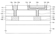
図1は本発明による金属配線構造の一実施例を示した断面図である。 FIG. 1 is a sectional view showing an embodiment of a metal wiring structure according to the present invention.
図1を参照すれば、第1層間絶縁膜106内に相互離隔された第1下部金属配線膜パターン108a及び第2下部金属配線膜パターン108bが配される。図面上では、第1下部金属配線膜パターン108a及び第2下部金属配線膜パターン108bは相互離隔されているが、図示されていない他の部分で相互連結されることもある。また、第1下部金属配線膜パターン108a及び第2下部金属配線膜パターン108bは絶縁膜104を介在して半導体基板102から分離されているが、図示されていない他の部分でのコンタクトを介して半導体基板102の所定領域、例えばアクティブ領域と連結されるのが一般的である。第1下部金属配線膜パターン108a及び第2下部金属配線膜パターン108bは銅膜パターンであるが、必ずしもこれに限定されるものではない。
Referring to FIG. 1, a first lower metal
第1層間絶縁膜106と、第1下部金属配線膜パターン108a及び第2下部金属配線膜パターン108b上には金属間絶縁膜112が配される。金属間絶縁膜112は低誘電率、例えば3以下の誘電率を有する低誘電体物質膜である。このように低誘電率を有する低誘電体物質膜を金属間絶縁膜112として使用することによってRC遅延時間を縮められる。金属間絶縁膜112は第1ビアコンタクトホール120a及び第2ビアコンタクトホール120bを有する。第1ビアコンタクトホール120aは金属間絶縁膜112を貫通して第1下部金属配線膜パターン108aの一部表面を露出させる。第2ビアコンタクトホール120bは金属間絶縁膜112を貫通して第2下部金属配線膜パターン108bの一部表面を露出させる。一方、金属間絶縁膜112下部には第1エッチング停止膜110が配される。第1エッチング停止膜110は第1ビアコンタクトホール120a及び第2ビアコンタクトホール120b形成のためのエッチング工程時にエッチング停止のために設けられる膜である。
An intermetal
金属間絶縁膜112上には第2層間絶縁膜116が配される。第2層間絶縁膜116は第1トレンチ118a及び第2トレンチ118bを有する。第1トレンチ118aは第2層間絶縁膜116を貫通して第1ビアコンタクトホール120aを完全に露出させる。したがって、第1トレンチ118aの幅または断面積は第1ビアコンタクトホール120aの幅または断面積より広い。第2トレンチ118bは第2層間絶縁膜116を貫通して第2ビアコンタクトホール120bを完全に露出させる。したがって、第2トレンチ118bの幅または断面積は第2ビアコンタクトホール120bの幅または断面積より広い。第2トレンチ118bの幅または断面積は、第1トレンチ118aの幅または断面積より顕著に広いが、その差については後述する。
A second interlayer
一方、第2層間絶縁膜116下部には第2エッチング停止膜114が配される。第2エッチング停止膜114は第1トレンチ118a及び第2トレンチ118bの形成のためのエッチング工程時にエッチング停止のために設けられる膜である。
Meanwhile, a second
第1ビアコンタクトホール120a及び第1トレンチ118a内部と第1下部金属配線膜パターン108aの露出表面上には第1障壁金属層122aが配される。第1障壁金属層122aは第1ビアコンタクトホール120a内部を充填する第1上部金属配線膜124aからの金属成分が金属間絶縁膜112に浸透して入っていく現象を防止するためのものもあり、この他にも公知のさまざまな利点を提供する。第1障壁金属層122aは、タンタル膜、窒化タンタル膜、チタン膜及び窒化チタン膜のうち少なくともいずれか一つを含む単層膜または多層膜である。
A first
第1障壁金属層122a上には第1上部金属配線膜パターン124aが配される。第1上部金属配線膜パターン124aは第1ビアコンタクトホール120a及び第1トレンチ118a内部を完全に充填する。第1上部金属配線膜パターン124aは銅膜パターンであるが、必ずしもこれに限定されるものではない。
A first upper metal
第2ビアコンタクトホール120b及び第2トレンチ118b内部と第2下部金属配線膜パターン108bの露出表面上には第2障壁金属層122bが配される。第2障壁金属層122bは、前述の第1障壁金属層122aと同様に第2ビアコンタクトホール120b内部を充填する第2上部金属配線膜124bからの金属成分が金属間絶縁膜112に侵入して入っていく現象を防止するためのものであり、この他にも公知のさまざまな利点を提供する。第2障壁金属層122aもタンタル膜、窒化タンタル膜、チタン膜及び窒化チタン膜のうち少なくともいずれか一つを含む単層膜または多層膜である。
A second
第2障壁金属層122b上には第2上部金属配線膜パターン124bが配される。第2上部金属配線膜パターン124bは銅膜パターンであるが、必ずしもこれに限定されるものではない。この第2上部金属配線膜パターン124bは第2ビアコンタクトホール120b内部を完全に充填するが、第2トレンチ118b内部は完全に充填できずに一部だけを充填する。その結果、第2上部金属配線膜パターン124bにより第2トレンチ118b内には第3トレンチ126が設けられる。第3トレンチ126が第2トレンチ118bより狭い幅または断面積を有するということは当然である。
A second upper metal
第3トレンチ126内でボイド拡散防止膜128が第2上部金属配線膜パターン124b上に形成される。そして、ボイド拡散防止膜128上には第3上部金属配線膜パターン130bが第3トレンチ126を充填しつつ配される。第3上部金属配線膜パターン130bは、第2上部金属配線膜パターン124bのような銅膜パターンであるが、必ずしもこれに限定されるものではない。第3上部金属配線膜パターン130bの厚さは第2上部金属配線膜パターン124bの厚さの少なくとも5倍以上である。望ましくは、第2上部金属配線膜パターン124bの厚さはほぼ1000Åほどであり、第3上部金属配線膜パターン130bの厚さはほぼ7000Åほどである。
A void
前記ボイド拡散防止膜128は、第3上部金属配線膜パターン130b内に存在するボイドを第2ビアコンタクトホール120b内に移動させないための膜である。このボイド拡散防止膜128は、タンタル膜、チタン膜及びアルミニウム膜のうち少なくともいずれか一つを含む単層膜または多層膜である。
The void
前記金属配線構造は、デュアルダマシン工程により設けられうる金属配線構造である。デュアルダマシン工程を使用して金属配線構造を形成するにあたり、上部金属配線膜パターンが十分な幅または広さを有する場合、上部金属配線膜パターン内に存在するボイドが応力勾配によりビアコンタクトホール内に流入されて合わさり、その結果ビアコンタクトホール内に大きなボイドが設けられうるということはすでに説明した。しかし、実施例による金属配線構造において、第1上部金属配線膜パターン124aは比較的狭い幅または断面積を有するが、その程度は第1上部金属配線膜パターン124a内のボイド密度が低く、たとえある程度の応力勾配が存在したとしても、ボイドが第1ビアコンタクトホール120a内部に円滑に流入されない程度である。一方、第2及び第3上部金属配線膜パターン124b,130bは、第1上部金属配線膜パターン124aに比べて比較的広い幅または断面積を有するが、その程度は第2及び第3上部金属配線膜パターン124b,130b内のボイド密度が高く、このボイドが第2ビアコンタクトホール120b内部に円滑に流入される程度である。
The metal wiring structure is a metal wiring structure that can be provided by a dual damascene process. When forming the metal wiring structure using the dual damascene process, if the upper metal wiring film pattern has a sufficient width or width, voids existing in the upper metal wiring film pattern are formed in the via contact hole due to the stress gradient. It has already been explained that large voids can be provided in the via contact holes as a result of the inflows. However, in the metal wiring structure according to the embodiment, the first upper metal
本実施例による金属配線構造において、比較的狭い幅または断面積を有してボイド密度が低い領域、すなわち図面の左側配線領域では別のボイド拡散防止膜がなくとも、第1ビアコンタクトホール120a内にボイドが発生しない。そして、比較的広い幅または断面積を有してボイド密度が高い領域、すなわち図面の右側配線領域では第2上部金属配線膜パターン124bと第3上部金属配線膜パターン130b間にボイド拡散防止膜128が配されることにより、第3上部金属配線膜パターン130b内に多量に分布しているボイドが第2ビアコンタクトホール120b内部に流入できず、その結果第2ビアコンタクトホール120b内にもボイドが発生しない。
In the metal wiring structure according to the present embodiment, a region having a relatively narrow width or cross-sectional area and a low void density, that is, the left wiring region in the drawing, in the first via
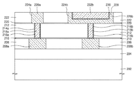
図2は本発明による金属配線構造の他の実施例を示した断面図である。本実施例による金属配線構造はシングルダマシン工程を適用して設けられる金属配線構造という点でデュアルダマシン工程を適用した図1の実施例とは異なる。 FIG. 2 is a sectional view showing another embodiment of the metal wiring structure according to the present invention. The metal wiring structure according to this embodiment is different from the embodiment of FIG. 1 in which the dual damascene process is applied in that it is a metal wiring structure provided by applying a single damascene process.
図2を参照すれば、第1層間絶縁膜206内に相互離隔された第1下部金属配線膜パターン208a及び第2下部金属配線膜パターン208bが配される。図面上では、第1下部金属配線膜パターン208a及び第2下部金属配線膜パターン208bは相互離隔されているが、図示されていない他の部分で相互連結されることもある。また第1下部金属配線膜パターン208a及び第2下部金属配線膜パターン208bは絶縁膜204を介して半導体基板202から分離されているが、図示されていない他の部分でのコンタクトを介して半導体基板202の所定領域、例えばアクティブ領域と連結されることが一般的である。第1下部金属配線膜パターン208a及び第2下部金属配線膜パターン208bは銅膜パターンであるが、必ずしもこれに限定されるものではない。
Referring to FIG. 2, a first lower metal
第1層間絶縁膜206と、第1下部金属配線膜パターン208a及び第2下部金属配線膜パターン208b上には金属間絶縁膜212が配される。金属間絶縁膜212は低誘電率、例えば3以下の誘電率を有する低誘電体物質膜である。金属間絶縁膜212は第1ビアコンタクトホール214a及び第2ビアコンタクトホール214bを有する。第1ビアコンタクトホール214aは金属間絶縁膜212を貫通して第1下部金属配線膜パターン208aの一部表面を露出させる。第2ビアコンタクトホール214bは金属間絶縁膜212を貫通して第2下部金属配線膜パターン208bの一部表面を露出させる。一方、金属間絶縁膜212の下部には第1エッチング停止膜210が配される。第1エッチング停止膜210は第1ビアコンタクトホール214a及び第2ビアコンタクトホール214b形成のためのエッチング工程時にエッチング停止のために設けられる膜である。
An
第1ビアコンタクトホール214aの内部面と第1下部金属配線膜パターン208aの露出面上には第1障壁金属層216aが配される。第1障壁金属層216aは、タンタル膜、窒化タンタル膜、チタン膜及び窒化チタン膜のうち少なくともいずれか一つを含む単層膜または多層膜である。第1障壁金属層216a上には第1ビアコンタクト218aが形成される。第1ビアコンタクト218aは、上下部の金属配線パターンを連結させるものであり、金属膜のような導電性物質膜であり、第1ビアコンタクトホール214a内部を完全に充填する。
A first
同様に、第2障壁金属層216bが第2ビアコンタクトホール214bの内部面と第2下部金属配線膜パターン208bの露出面上に配される。第2障壁金属層216bは、タンタル膜、窒化タンタル膜、チタン膜及び窒化チタン膜のうち少なくともいずれか一つを含む単層膜または多層膜である。第2障壁金属層216b上には第2ビアコンタクト218bが形成される。第2ビアコンタクト218bもまた上下部の金属配線パターンを連結させるものであり、金属膜のような導電性物質膜であり、第2ビアコンタクトホール214bの内部を完全に充填する。
Similarly, the second
金属間絶縁膜212上には第2層間絶縁膜222が配される。第2層間絶縁膜222は第1トレンチ224a及び第2トレンチ224bを有する。第1トレンチ224aは第2層間絶縁膜222を貫通して第1ビアコンタクト218aの上部面とその周囲の金属間絶縁膜212の一部とを露出させる。第2トレンチ224bは第2層間絶縁膜222を貫通して第2ビアコンタクト218bの上部面とその周囲の金属間絶縁膜212の一部とを露出させる。第2トレンチ224bの幅または断面積は、第1トレンチ224aの幅または断面積より顕著に広いが、その差については前述のようにボイド密度の差と関係がある。一方、第2層間絶縁膜222の下部には第2エッチング停止膜220が配される。第2エッチング停止膜220は、第1トレンチ224a及び第2トレンチ224b形成のためのエッチング工程時にエッチング停止のために設けられる膜である。
A second
第1トレンチ224a内には第1上部金属配線膜パターン226aが配される。第1上部金属配線膜パターン226aの下部面は第1ビアコンタクト218aの上部面とコンタクトされる。第2上部金属配線膜パターン226aは銅膜パターンであるが、必ずしもこれに限定されるものではない。
A first upper metal
第2トレンチ224b内には第2上部金属配線膜パターン226b、ボイド拡散防止膜230及び第3上部金属配線膜パターン232bが順次に配される。第2上部金属配線膜パターン226bは銅膜パターンであるが、必ずしもこれに限定されるものではない。具体的に、第2上部金属配線膜パターン226bの下部面は第2ビアコンタクト218bの上部面とコンタクトされ、第2トレンチ224bの内部を完全に充填できずに一部だけを充填する。その結果、第2上部金属配線膜パターン226bにより第2トレンチ224b内には第3トレンチ228が設けられる。第3トレンチ228が第2トレンチ224bより狭い幅または断面積を有するということは当然である。第3トレンチ228内でボイド拡散防止膜230が第2上部金属配線膜パターン226b上に形成され、ボイド拡散防止膜230上には第3上部金属配線膜パターン232bが第3トレンチ228が完全に充填されるように配される。
A second upper metal
第3上部金属配線膜パターン232bは、第2上部金属配線膜パターン226bのような銅膜パターンであるが、必ずしもこれに限定されるものではない。第3上部金属配線膜パターン232bの厚さは第2上部金属配線膜パターン226bの厚さの少なくとも5倍以上である。望ましくは、第2上部金属配線膜パターン226bの厚さはほぼ1000Åほどであり、第3上部金属配線膜パターン232bの厚さはほぼ7000Åほどである。前記ボイド拡散防止膜230は、第3上部金属配線膜パターン232b内に存在するボイドを第2ビアコンタクト218b内に移動させないための膜であるということは前述のところと同一である。このボイド拡散防止膜230は、タンタル膜、チタン膜及びアルミニウム膜のうち少なくともいずれか一つを含む単層膜または多層膜である。
The third upper metal
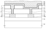
図3ないし図6は本発明による金属配線方法の一実施例を説明するために示した断面図である。本実施例による金属配線方法はデュアルダマシン工程を適用する配線方法である。 FIGS. 3 to 6 are cross-sectional views illustrating a metal wiring method according to an embodiment of the present invention. The metal wiring method according to the present embodiment is a wiring method to which a dual damascene process is applied.
まず図3を参照すれば、第1層間絶縁膜102内に相互離隔された第1下部金属配線膜パターン108a及び第2下部金属配線膜パターン108bを形成する。第1下部金属配線膜パターン108a及び第2下部金属配線膜パターン108bは、絶縁膜104により半導体基板102と分離されているように図示されているが、実質的には半導体基板102内の一定領域、例えばアクティブ領域に電気的に連結される。また、第1下部金属配線膜パターン108a及び第2下部金属配線膜パターン108bと半導体基板102間には絶縁膜104以外にも他の複数個の膜が形成されることもある。前記第1下部金属配線膜パターン108a及び第2下部金属配線膜パターン108bは銅膜パターンより形成できる。
First, referring to FIG. 3, a first lower metal
次に図4を参照すれば、第1層間絶縁膜102、第1下部金属配線膜パターン108a及び第2下部金属配線膜パターン108b上に第1ビアコンタクトホール120a及び第2ビアコンタクトホール120bを有する金属間絶縁膜112を形成する。そして、金属間絶縁膜112上に第1トレンチ118a及び第2トレンチ118bを有する第2層間絶縁膜116を形成する。このためにまず、第1層間絶縁膜102、第1下部金属配線膜パターン108a及び第2下部金属配線膜パターン108b上に第1エッチング停止膜110、金属間絶縁膜112、第2エッチング停止膜114及び第2層間絶縁膜116を順次に積層する。次に、第2層間絶縁膜116上に第1マスク膜パターン(図示せず)を形成する。この第1マスク膜パターン(図示せず)は第1トレンチ118a及び第2トレンチ118bが設けられる部分の第2層間絶縁膜116を露出させる。次に、前記第1マスク膜パターン(図示せず)をエッチングマスクとしたエッチング工程を行って第2層間絶縁膜116の露出部分を除去する。このエッチング工程は第2エッチング停止膜114の一部表面が露出されるまでなされる。それにより、比較的狭い幅の第1トレンチ118a及び比較的広い幅の第2トレンチ118bが設けられる。
Next, referring to FIG. 4, a first via
第1トレンチ118a及び第2トレンチ118bが設けられれば、第1マスク膜パターン(図示せず)を除去し、露出された第2エッチング停止膜114を除去して金属間絶縁膜112の一部表面を露出させる。場合により、第1マスク膜パターンは第2エッチング停止膜114を除去した後に除去することもある。
If the
次に、全面に第2マスク膜パターン(図示せず)を形成する。この第2マスク膜パターン(図示せず)は第1ビアコンタクトホール120a及び第2ビアコンタクトホール120bが設けられる部分の金属間絶縁膜112を露出させる。次に、前記第2マスク膜パターン(図示せず)をエッチングマスクとしたエッチング工程を行って金属間絶縁膜112の露出部分を除去する。このエッチング工程は第1エッチング停止膜110の一部表面が露出されるまでなされる。それにより、第1トレンチ118a及び第2トレンチ118b内にそれぞれ第1ビアコンタクトホール120a及び第2ビアコンタクトホール120bが形成される。次に、第2マスク膜パターン(図示せず)を除去し、露出された第1エッチング停止膜110を除去して第1下部金属配線膜108a及び第2下部金属配線膜108bの一部表面を露出させる。場合により、第2マスク膜パターンは第1エッチング停止膜110を除去した後に除去することもある。
Next, a second mask film pattern (not shown) is formed on the entire surface. The second mask film pattern (not shown) exposes the
次に図5を参照すれば、全面に障壁金属層122を形成する。この障壁金属層122はタンタル膜、窒化タンタル膜、チタン膜及び窒化チタン膜のうち少なくともいずれか一つが含まれるように形成する。次に、第1上部金属配線膜124を形成する。第1上部金属配線膜124は、電気メッキ法を使用して形成する。すなわち、全面に金属シード層を形成し、この金属シード層を陰極としてメッキ液との化学反応を発生させることによってメッキ液からの金属イオンを金属シード層表面に蒸着させる。この場合、第1ビアコンタクトホール120a及び第2ビアコンタクトホール120bの内部は第1上部金属配線膜124により完全に充填される。そして、第1トレンチ118aも比較的狭い幅または断面積を有するので、その内部が第1上部金属配線膜124により完全に充填される。しかし、比較的広い幅または断面積を有する第2トレンチ118bの場合には、第1上部金属配線膜124によりその内部が完全に充填されず、従って第2トレンチ118b内部の第3トレンチ126が設けられる。
Next, referring to FIG. 5, a
次に図6を参照すれば、第1上部金属配線膜124上にボイド拡散防止膜128及び第2上部金属配線膜130を順次に形成する。このボイド拡散防止膜128は、第2上部金属配線膜130内に存在するボイドを第1上部金属配線膜124を介して第2ビアコンタクトホール120b内に流入させないためのものである。ボイド拡散防止膜128はタンタル膜、チタン膜及びアルミニウム膜のうち少なくともいずれか一つを含み、特にアルミニウム膜は金属配線膜の結晶粒界に偏析されてボイドと拡散防止にさらに効果的である。ボイド拡散防止膜128は物理的気相蒸着(PVD:Physical Vapor Deposition)法、化学的気相蒸着(CVD:Chemical Vapor Deposition)法または原子層蒸着(ALD:Atomic Layer Deposition)法を使用して形成する。ボイド拡散防止膜128及び第2上部金属配線膜130を形成した後には平坦化工程を行う。平坦化工程としては、公知の化学的機械的平坦化(CMP:Chemical Mechanical Polishing)法を使用し、「A」と示された点線上に存在する全てのものを除去する。それにより、図1に図示されたように、第1上部金属配線膜(図6の124)は第1ビアコンタクトホール120a及び第1トレンチ118a内の第1上部金属配線膜パターン124aと、第2ビアコンタクトホール120b及び第2トレンチ118b内の第2上部金属配線膜パターン124bとに分離され、第2上部金属配線膜(図6の130)は第3トレンチ126内の第3上部金属配線膜パターン130bとしてだけ残る。
Next, referring to FIG. 6, a void
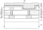
図7ないし図9は本発明による金属配線方法の他の実施例を説明するために示した断面図である。本実施例による金属配線方法はシングルダマシン工程を適用する配線方法である。 7 to 9 are cross-sectional views for explaining another embodiment of the metal wiring method according to the present invention. The metal wiring method according to the present embodiment is a wiring method to which a single damascene process is applied.
まず図7を参照すれば、第1層間絶縁膜202内に相互離隔された第1下部金属配線膜パターン208a及び第2下部金属配線膜パターン208bを形成する。本実施例においても、第1下部金属配線膜パターン208a及び第2下部金属配線膜パターン208bは、実質的に半導体基板202内の一定領域、例えばアクティブ領域に電気的に連結される。また、第1下部金属配線膜パターン208a及び第2下部金属配線膜パターン208bと半導体基板202間には絶縁膜204以外にも他の複数個の膜が形成されることもある。前記第1下部金属配線膜パターン208a及び第2下部金属配線膜パターン208bは銅膜パターンより形成できる。
First, referring to FIG. 7, a first lower metal
次に、第1層間絶縁膜202、第1下部金属配線膜パターン208a及び第2下部金属配線膜パターン208b上に第1エッチング停止膜210及び金属間絶縁膜212を順次に形成する。そして、所定のエッチングマスク膜パターンを利用したエッチング工程を行って金属間絶縁膜212の一部を除去する。このエッチング工程は第1エッチング停止膜210の一部表面が露出されるまで行われる。次に、露出された第1エッチング停止膜210を除去すれば、第1下部金属配線膜パターン208aの一部表面を露出させる第1ビアコンタクトホール214a及び第2下部金属配線膜パターン208bの一部表面を露出させる第2ビアコンタクトホール214bが設けられる。
Next, a first
次に、障壁金属層を全面に形成し、続いて第1ビアコンタクトホール214a及び第2ビアコンタクトホール214bが充填されるようにコンタクト用金属膜を障壁金属層上に形成する。障壁金属層はタンタル膜、窒化タンタル膜、チタン膜及び窒化チタン膜のうち少なくともいずれか一つが含まれるように形成する。次に、1次平坦化工程を行って金属間絶縁膜212の表面を露出させる。それにより、障壁金属層は第1ビアコンタクトホール214a内の第1障壁金属層216aと、第2ビアコンタクトホール214b内の第2障壁金属層216bとに分離される。また、コンタクト用金属膜も第1ビアコンタクトホール214a内の第1ビアコンタクト218aと、第2ビアコンタクトホール214b内の第2ビアコンタクト218bとに分離される。
Next, a barrier metal layer is formed on the entire surface, and then a contact metal film is formed on the barrier metal layer so as to fill the first via
次に図8を参照すれば、金属間絶縁膜212、第1ビアコンタクト218a及び第2ビアコンタクト218bの上部面上に第2エッチング停止膜220及び第2層間絶縁膜222を順次に形成する。次に、所定のエッチングマスク膜パターンを利用したエッチング工程を行って第2層間絶縁膜222の一部を除去する。このエッチング工程は第2エッチング停止膜220の一部表面が露出されるまで行われる。次に、露出された第2エッチング停止膜220を除去すれば、第1ビアコンタクト218aの上部面を完全に露出させる第1トレンチ224a及び第2ビアコンタクト218bの上部面を完全に露出させる第2トレンチ224bが設けられる。第1トレンチ224aの幅または断面積は第2トレンチ224bの幅または断面積より小さい。
Referring to FIG. 8, a second
次に、全面に第1上部金属配線膜226を形成する。第1上部金属配線膜226は、電気メッキ法を使用して形成する。すなわち、全面に金属シード層を形成し、この金属シード層を陰極としてメッキ液との化学反応を発生させることにより、メッキ液からの金属イオンを金属シード層表面に蒸着させる。この場合、狭い幅または断面積を有する第1トレンチ224a内部は第1上部金属配線膜226により完全に充填される。しかし、広い幅または断面積を有する第2トレンチ224bの場合には、第1上部金属配線膜226によりその内部が完全に充填されず、従って第2トレンチ224b内部の第3トレンチ228が設けられる。
Next, a first upper
次に図9を参照すれば、第1上部金属配線膜226上にボイド拡散防止膜230及び第2上部金属配線膜232を順次に形成する。このボイド拡散防止膜230は、第2上部金属配線膜232内に存在するボイドを第1上部金属配線膜226を介して第2ビアコンタクト218b内部に流入させないためのものである。ボイド拡散防止膜230はタンタル膜、チタン膜及びアルミニウム膜のうち少なくともいずれか一つを含み、特にアルミニウム膜は金属配線膜の結晶粒界に偏析されてボイドの拡散防止にさらに効果的である。ボイド拡散防止膜230はPVD法、CVD法またはALD法を使用して形成する。ボイド拡散防止膜230及び第2上部金属配線膜232を形成した後には平坦化工程を行う。平坦化工程としてはCMP法を使用し、「A」と示された点線上に存在する全てのものを除去する。それにより、図2に図示されたように、第1上部金属配線膜(図9の226)は第1トレンチ224a内の第1上部金属配線膜パターン226aと、第2トレンチ224b内の第2上部金属配線膜パターン226bとに分離され、第2上部金属配線膜(図9の232)は第3トレンチ228内の第3上部金属配線膜パターン232bとしてだけ残る。
Next, referring to FIG. 9, a void
以上、本発明を望ましい実施例を挙げて詳細に説明したが、本発明は前記実施例に限定されず、本発明の技術的思想内で当分野で当業者によってさまざまな変形が可能であることは明らかである。 The present invention has been described in detail with reference to the preferred embodiments. However, the present invention is not limited to the above-described embodiments, and various modifications can be made by those skilled in the art within the technical idea of the present invention. Is clear.
本発明は金属配線を有する半導体素子を利用するあらゆる産業分野に適用できる。 The present invention can be applied to all industrial fields using semiconductor elements having metal wiring.
102、202 半導体基板、
104、204 絶縁膜、
106、206 第1層間絶縁膜、
108a、208a 第1下部金属配線膜パターン、
108b、208b 第2下部金属配線膜パターン、
110、210 第1エッチング停止膜、
112、212 金属間絶縁膜、
114、220 第2エッチング停止膜、
116、222 第2層間絶縁膜、
118a、224a 第1トレンチ、
118b、224b 第2トレンチ、
120a、214a 第1ビアコンタクトホール、
120b、214b 第2ビアコンタクトホール、
122a、216a 第1障壁金属層、
122b、216b 第2障壁金属層、
124a、226a 第1上部金属配線膜パターン、
124b、226b 第2上部金属配線膜パターン、
128、230 ボイド拡散防止膜、
130b、232b 第3上部金属配線膜パターン、
218a 第1ビアコンタクト、
218b 第2ビアコンタクト、
228 第3トレンチ。
102, 202 Semiconductor substrate,
104, 204 insulating film,
106, 206 first interlayer insulating film,
108a, 208a first lower metal wiring film pattern,
108b, 208b second lower metal wiring film pattern,
110, 210 first etching stop film,
112, 212 Intermetal insulating film,
114, 220 Second etching stop film,
116, 222 second interlayer insulating film,
118a, 224a first trench,
118b, 224b second trench,
120a, 214a First via contact hole,
120b, 214b Second via contact hole,
122a, 216a first barrier metal layer,
122b, 216b second barrier metal layer,
124a, 226a first upper metal wiring film pattern,
124b, 226b second upper metal wiring film pattern,
128, 230 void diffusion prevention film,
130b, 232b Third upper metal wiring film pattern,
218a first via contact,
218b second via contact,
228 Third trench.
Claims (4)
前記第1層間絶縁膜及び下部金属膜パターン上で前記下部金属膜パターンの一部表面を露出させるビアコンタクトホールを有する金属間絶縁膜と、
前記ビアコンタクトホール内部面及び前記下部金属配線膜パターンの露出表面上に形成された障壁金属層と、
前記障壁金属層上で前記ビアコンタクトホール内部を充填するビアコンタクトと、
前記金属間絶縁膜及びビアコンタクト上で前記金属間絶縁膜の一部表面及びビアコンタクトの上部表面を露出させるトレンチを有する第2層間絶縁膜と、
前記金属間絶縁膜及び前記ビアコンタクト上で前記トレンチの底面および側面を被覆する、第1厚さの第1上部金属配線膜パターンと、
前記第1上部金属配線膜パターン上に形成されたボイド拡散防止膜と、
前記ボイド拡散防止膜上で前記トレンチ内部を全て充填する第2厚さの第2上部金属配線膜パターンとを備え、
前記第1上部金属配線膜パターンと第2上部金属配線膜パターンとは、同一の金属から形成され、
前記第1上部金属配線膜パターンの側壁は、前記第2層間絶縁膜と接することを特徴とする金属配線構造。 A lower metal wiring film pattern disposed in the first interlayer insulating film;
An intermetal insulating film having a via contact hole exposing a part of a surface of the lower metal film pattern on the first interlayer insulating film and the lower metal film pattern;
A barrier metal layer formed on an inner surface of the via contact hole and an exposed surface of the lower metal wiring film pattern;
A via contact filling the inside of the via contact hole on the barrier metal layer;
A second interlayer insulating film having a trench exposing a part of the intermetallic insulating film and an upper surface of the via contact on the intermetallic insulating film and the via contact;
A first upper metal wiring film pattern having a first thickness covering a bottom surface and a side surface of the trench on the intermetal insulating film and the via contact;
A void diffusion prevention film formed on the first upper metal wiring film pattern;
A second upper metal wiring film pattern having a second thickness filling the inside of the trench on the void diffusion prevention film;
The first upper metal wiring film pattern and the second upper metal wiring film pattern are formed of the same metal ,
The metal wiring structure according to claim 1, wherein a sidewall of the first upper metal wiring film pattern is in contact with the second interlayer insulating film .
前記第1層間絶縁膜と前記第1及び第2下部金属配線膜パターン上に形成され、前記第1下部金属配線膜パターンの一部表面を露出させる第1ビアコンタクトホール及び前記第2下部金属配線膜パターンの一部表面を露出させる第2ビアコンタクトホールを含む、ビアコンタクトホールのみを有する金属間絶縁膜と、
前記第1ビアコンタクトホール及び第2ビアコンタクトホール内にそれぞれ形成された第1及び第2障壁金属層と、
前記第1及び第2障壁金属層上でそれぞれ第1及び第2ビアコンタクトホールを充填するように形成された第1及び第2ビアコンタクトと、
前記金属間絶縁膜上に形成され、前記第1ビアコンタクトの上部面を露出させる第1トレンチ及び前記第2ビアコンタクトの上部面を露出させる第2トレンチを有する第2層間絶縁膜と、
前記第1トレンチを充填するように形成された第1上部金属配線膜パターンと、
前記第2トレンチの底面および側面を被覆するように前記第2障壁金属層上に形成されることによって、前記第2トレンチ内の第3トレンチを形成させる第2上部金属配線膜パターンと、
前記第2上部金属配線膜パターン上に形成されたボイド拡散防止層と、
前記ボイド拡散防止層上で前記第3トレンチを充填する第3上部金属配線膜パターンとを含むことを特徴とする金属配線膜構造。
First and second lower metal wiring film patterns disposed in a first region and a second region, respectively, separated from each other in the first interlayer insulating film;
A first via contact hole and a second lower metal wiring formed on the first interlayer insulating film and the first and second lower metal wiring film patterns and exposing a part of the surface of the first lower metal wiring film pattern. An intermetallic insulating film having only via contact holes, including a second via contact hole exposing a part of the surface of the film pattern;
First and second barrier metal layers respectively formed in the first via contact hole and the second via contact hole;
First and second via contacts formed on the first and second barrier metal layers to fill the first and second via contact holes, respectively.
A second interlayer insulating film formed on the intermetal insulating film and having a first trench exposing the upper surface of the first via contact and a second trench exposing the upper surface of the second via contact;
A first upper metal wiring film pattern formed to fill the first trench;
By being formed before Symbol second barrier metal layer so as to cover the bottom and side surfaces of the second trench, and the second upper metal interconnection layer pattern to form a third trench in the second trench,
A void diffusion prevention layer formed on the second upper metal wiring layer pattern;
A metal wiring film structure comprising: a third upper metal wiring film pattern filling the third trench on the void diffusion preventing layer.
前記第1層間絶縁膜と前記第1及び第2下部金属配線膜パターン上に金属間絶縁膜を形成する段階と、
前記金属間絶縁膜の一部を除去し、前記第1及び第2下部金属配線膜パターンの一部表面をそれぞれ露出させる第1コンタクトホール及び第2コンタクトホールを形成する段階と、
前記金属間絶縁膜と前記第1及び第2下部金属配線膜パターンの露出表面上に障壁金属層を形成する段階と、
前記第1コンタクトホール及び第2コンタクトホールが充填されるように前記障壁金属層上に金属膜を形成する段階と、
平坦化を行い、前記金属膜を前記第1コンタクトホール内の第1ビアコンタクト及び前記第2コンタクトホール内の第2ビアコンタクトに分離させる段階と、
前記金属間絶縁膜、第1ビアコンタクト及び第2ビアコンタクト上に第2層間絶縁膜を形成する段階と、
前記第2層間絶縁膜の一部を除去し、前記第1ビアコンタクト及び第2ビアコンタクトの上部面をそれぞれ露出させる第1トレンチ及び第2トレンチを形成する段階と、
前記第1トレンチが充填されるように第1上部金属配線膜を形成し、前記第2トレンチ内部底面および側面を被覆するように前記障壁金属層上に第2上部金属配線膜を形成することにより、第3トレンチを形成させる段階と、
前記第3トレンチを有する第1上部金属配線膜上にボイド拡散防止層を形成する段階と、
前記第3トレンチが充填されるように前記ボイド拡散防止層上に第2上部金属配線膜を形成する段階と、
平坦化を行い、前記第1トレンチ内の第1上部金属配線膜と前記第2及び第3トレンチ内の第2及び第3上部金属配線膜とを分離させる段階とを含むことを特徴とする金属配線方法。 Forming first and second lower metal wiring layer patterns spaced apart from each other in the first interlayer insulating layer;
Forming an intermetal insulating film on the first interlayer insulating film and the first and second lower metal wiring film patterns;
Removing a part of the intermetal insulating film, and forming a first contact hole and a second contact hole exposing the partial surfaces of the first and second lower metal wiring film patterns, respectively;
Forming a barrier metal layer on the exposed surfaces of the intermetal insulating film and the first and second lower metal wiring film patterns;
Forming a metal film on the barrier metal layer so as to fill the first contact hole and the second contact hole;
Performing planarization and separating the metal film into a first via contact in the first contact hole and a second via contact in the second contact hole;
Forming a second interlayer insulating film on the intermetal insulating film, the first via contact and the second via contact;
Removing a part of the second interlayer insulating film and forming a first trench and a second trench exposing upper surfaces of the first via contact and the second via contact, respectively.
Forming a first upper metal wiring film so as to fill the first trench, and forming a second upper metal wiring film on the barrier metal layer so as to cover an inner bottom surface and a side surface of the second trench; Forming a third trench;
Forming a void diffusion prevention layer on the first upper metal wiring layer having the third trench;
Forming a second upper metal wiring layer on the void diffusion preventing layer so as to fill the third trench;
Planarizing and separating the first upper metal wiring film in the first trench and the second and third upper metal wiring films in the second and third trenches. Wiring method.
Applications Claiming Priority (2)
| Application Number | Priority Date | Filing Date | Title |
|---|---|---|---|
| KR1020030053890A KR100555513B1 (en) | 2003-08-04 | 2003-08-04 | Metal wiring structure and metal wiring method to prevent voids |
| KR2003-053890 | 2003-08-04 |
Publications (2)
| Publication Number | Publication Date |
|---|---|
| JP2005057277A JP2005057277A (en) | 2005-03-03 |
| JP4852234B2 true JP4852234B2 (en) | 2012-01-11 |
Family
ID=34114250
Family Applications (1)
| Application Number | Title | Priority Date | Filing Date |
|---|---|---|---|
| JP2004222508A Expired - Fee Related JP4852234B2 (en) | 2003-08-04 | 2004-07-29 | Metal wiring structure and metal wiring method in which void generation is prevented |
Country Status (4)
| Country | Link |
|---|---|
| US (1) | US6953745B2 (en) |
| JP (1) | JP4852234B2 (en) |
| KR (1) | KR100555513B1 (en) |
| CN (1) | CN100392853C (en) |
Families Citing this family (28)
| Publication number | Priority date | Publication date | Assignee | Title |
|---|---|---|---|---|
| TWI229411B (en) * | 2004-04-20 | 2005-03-11 | Powerchip Semiconductor Corp | Method of manufacturing a semiconductor device |
| US20060128147A1 (en) * | 2004-12-09 | 2006-06-15 | Honeywell International Inc. | Method of fabricating electrically conducting vias in a silicon wafer |
| JP2007081130A (en) * | 2005-09-14 | 2007-03-29 | Toshiba Corp | Manufacturing method of semiconductor device |
| US8368220B2 (en) * | 2005-10-18 | 2013-02-05 | Taiwan Semiconductor Manufacturing Co. Ltd. | Anchored damascene structures |
| KR100660325B1 (en) * | 2005-11-15 | 2006-12-22 | 동부일렉트로닉스 주식회사 | Manufacturing method of semiconductor device |
| US7514354B2 (en) | 2005-12-30 | 2009-04-07 | Samsung Electronics Co., Ltd | Methods for forming damascene wiring structures having line and plug conductors formed from different materials |
| KR100928507B1 (en) * | 2007-12-03 | 2009-11-26 | 주식회사 동부하이텍 | Manufacturing Method of Semiconductor Device |
| JP2009278000A (en) * | 2008-05-16 | 2009-11-26 | Toshiba Corp | Semiconductor device and method of manufacturing semiconductor device |
| KR101030663B1 (en) * | 2008-06-27 | 2011-04-20 | 주식회사 하이닉스반도체 | Metal wiring formation method of semiconductor device |
| JP2010171170A (en) * | 2009-01-22 | 2010-08-05 | Hitachi Cable Ltd | Copper circuit wiring board and method for manufacturing the same |
| TWI392405B (en) * | 2009-10-26 | 2013-04-01 | Unimicron Technology Corp | Circuit structure |
| KR101300587B1 (en) * | 2009-12-09 | 2013-08-28 | 한국전자통신연구원 | Method for forming semiconductor device |
| US8304863B2 (en) * | 2010-02-09 | 2012-11-06 | International Business Machines Corporation | Electromigration immune through-substrate vias |
| CN102196673B (en) * | 2010-03-05 | 2013-10-16 | 欣兴电子股份有限公司 | Method for manufacturing circuit structure |
| KR101697573B1 (en) * | 2010-11-29 | 2017-01-19 | 삼성전자 주식회사 | Semiconductor device, fabricating method thereof, and semiconductor package comprising the semiconductor device |
| CN102420171A (en) * | 2011-05-13 | 2012-04-18 | 上海华力微电子有限公司 | Dual damascene manufacturing process for super-thick top-layer metal |
| US9269612B2 (en) * | 2011-11-22 | 2016-02-23 | Taiwan Semiconductor Manufacturing Company, Ltd. | Mechanisms of forming damascene interconnect structures |
| US8710660B2 (en) * | 2012-07-20 | 2014-04-29 | Taiwan Semiconductor Manufacturing Company, Ltd. | Hybrid interconnect scheme including aluminum metal line in low-k dielectric |
| US8772934B2 (en) * | 2012-08-28 | 2014-07-08 | Taiwan Semiconductor Manufacturing Company, Ltd. | Aluminum interconnection apparatus |
| US9252110B2 (en) * | 2014-01-17 | 2016-02-02 | Taiwan Semiconductor Manufacturing Company, Ltd. | Interconnect structure and method of forming same |
| US9530737B1 (en) * | 2015-09-28 | 2016-12-27 | Taiwan Semiconductor Manufacturing Co., Ltd. | Semiconductor device and manufacturing method thereof |
| US9824970B1 (en) * | 2016-06-27 | 2017-11-21 | Globalfoundries Inc. | Methods that use at least a dual damascene process and, optionally, a single damascene process to form interconnects with hybrid metallization and the resulting structures |
| CN110137153B (en) * | 2018-02-09 | 2021-03-30 | 联华电子股份有限公司 | Semiconductor device and method of forming the same |
| US10811353B2 (en) * | 2018-10-22 | 2020-10-20 | International Business Machines Corporation | Sub-ground rule e-Fuse structure |
| US10734338B2 (en) * | 2018-11-23 | 2020-08-04 | Nanya Technology Corporation | Bonding pad, semiconductor structure, and method of manufacturing semiconductor structure |
| KR102675935B1 (en) * | 2019-12-16 | 2024-06-18 | 삼성전자주식회사 | Semiconductor device |
| CN114126225B (en) * | 2020-08-31 | 2024-12-17 | 庆鼎精密电子(淮安)有限公司 | Method for manufacturing circuit board, circuit board and method for manufacturing circuit board |
| US11488905B2 (en) * | 2020-12-08 | 2022-11-01 | Nanya Technology Corporation | Semiconductor device structure with manganese-containing conductive plug and method for forming the same |
Family Cites Families (20)
| Publication number | Priority date | Publication date | Assignee | Title |
|---|---|---|---|---|
| JP3391933B2 (en) * | 1995-04-27 | 2003-03-31 | 沖電気工業株式会社 | Semiconductor device and manufacturing method thereof |
| US6174810B1 (en) * | 1998-04-06 | 2001-01-16 | Motorola, Inc. | Copper interconnect structure and method of formation |
| US6214696B1 (en) * | 1998-04-22 | 2001-04-10 | Texas Instruments - Acer Incorporated | Method of fabricating deep-shallow trench isolation |
| JP2943805B1 (en) * | 1998-09-17 | 1999-08-30 | 日本電気株式会社 | Semiconductor device and manufacturing method thereof |
| JP4044236B2 (en) * | 1999-03-11 | 2008-02-06 | 株式会社東芝 | Manufacturing method of semiconductor device |
| US6144099A (en) * | 1999-03-30 | 2000-11-07 | Advanced Micro Devices, Inc. | Semiconductor metalization barrier |
| JP3365495B2 (en) * | 1999-06-30 | 2003-01-14 | 日本電気株式会社 | Semiconductor device and manufacturing method thereof |
| JP2001110809A (en) * | 1999-10-04 | 2001-04-20 | Toshiba Corp | Semiconductor device |
| US6184128B1 (en) * | 2000-01-31 | 2001-02-06 | Advanced Micro Devices, Inc. | Method using a thin resist mask for dual damascene stop layer etch |
| JP2002050688A (en) * | 2000-08-03 | 2002-02-15 | Seiko Epson Corp | Semiconductor device and method of manufacturing the same |
| KR20020053610A (en) | 2000-12-27 | 2002-07-05 | 박종섭 | Method of fabricating conductive lines and interconnections in semiconductor devices |
| US6713874B1 (en) * | 2001-03-27 | 2004-03-30 | Advanced Micro Devices, Inc. | Semiconductor devices with dual nature capping/arc layers on organic-doped silica glass inter-layer dielectrics |
| US6486059B2 (en) * | 2001-04-19 | 2002-11-26 | Silicon Intergrated Systems Corp. | Dual damascene process using an oxide liner for a dielectric barrier layer |
| JP2003031574A (en) * | 2001-07-13 | 2003-01-31 | Toshiba Corp | Semiconductor device and method of manufacturing the same |
| JP3540302B2 (en) * | 2001-10-19 | 2004-07-07 | Necエレクトロニクス株式会社 | Semiconductor device and manufacturing method thereof |
| JP3886779B2 (en) * | 2001-11-02 | 2007-02-28 | 富士通株式会社 | Insulating film forming material and insulating film forming method |
| JP2003218201A (en) * | 2002-01-24 | 2003-07-31 | Mitsubishi Electric Corp | Semiconductor device and method of manufacturing the same |
| JP2003282703A (en) * | 2002-03-26 | 2003-10-03 | Hitachi Ltd | Semiconductor device manufacturing method and semiconductor device |
| JP4272168B2 (en) * | 2003-03-28 | 2009-06-03 | 富士通マイクロエレクトロニクス株式会社 | Semiconductor device and semiconductor integrated circuit device |
| JP2004311865A (en) * | 2003-04-10 | 2004-11-04 | Renesas Technology Corp | Wiring structure |
-
2003
- 2003-08-04 KR KR1020030053890A patent/KR100555513B1/en not_active Expired - Fee Related
-
2004
- 2004-07-15 US US10/891,062 patent/US6953745B2/en not_active Expired - Lifetime
- 2004-07-29 JP JP2004222508A patent/JP4852234B2/en not_active Expired - Fee Related
- 2004-08-04 CN CNB2004100558141A patent/CN100392853C/en not_active Expired - Lifetime
Also Published As
| Publication number | Publication date |
|---|---|
| CN1581476A (en) | 2005-02-16 |
| CN100392853C (en) | 2008-06-04 |
| JP2005057277A (en) | 2005-03-03 |
| US6953745B2 (en) | 2005-10-11 |
| US20050029010A1 (en) | 2005-02-10 |
| KR100555513B1 (en) | 2006-03-03 |
| KR20050015190A (en) | 2005-02-21 |
Similar Documents
| Publication | Publication Date | Title |
|---|---|---|
| JP4852234B2 (en) | Metal wiring structure and metal wiring method in which void generation is prevented | |
| JP3887282B2 (en) | Metal-insulator-metal capacitor and method for manufacturing semiconductor device having damascene wiring structure | |
| US6251740B1 (en) | Method of forming and electrically connecting a vertical interdigitated metal-insulator-metal capacitor extending between interconnect layers in an integrated circuit | |
| KR100413828B1 (en) | Semiconductor device and method of making the same | |
| US6417535B1 (en) | Vertical interdigitated metal-insulator-metal capacitor for an integrated circuit | |
| US7709905B2 (en) | Dual damascene wiring and method | |
| US7214594B2 (en) | Method of making semiconductor device using a novel interconnect cladding layer | |
| JP7492618B2 (en) | Method for fabricating an integrated circuit having dual metal power rails - Patent 7523636 | |
| US6806579B2 (en) | Robust via structure and method | |
| KR20030035909A (en) | Semiconductor device and method for manufacturing the same | |
| US7932187B2 (en) | Method for fabricating a semiconductor device | |
| JP4338614B2 (en) | Semiconductor device and manufacturing method thereof | |
| USRE43320E1 (en) | Semiconductor device and manufacturing method thereof | |
| CN101471285A (en) | Semiconductor device and method for manufacturing the device | |
| JP2005311123A (en) | Semiconductor device and manufacturing method thereof | |
| US20040192008A1 (en) | Semiconductor device including interconnection and capacitor, and method of manufacturing the same | |
| KR100763760B1 (en) | Fabrication method of semiconductor device | |
| JP4110829B2 (en) | Manufacturing method of semiconductor device | |
| US6841471B2 (en) | Fabrication method of semiconductor device | |
| US7112537B2 (en) | Method of fabricating interconnection structure of semiconductor device | |
| KR100440472B1 (en) | Fabrication method of semiconductor device | |
| US6642139B1 (en) | Method for forming interconnection structure in an integration circuit | |
| JP2004356315A (en) | Semiconductor device and manufacturing method thereof | |
| JP2007158169A (en) | Multilayer wiring structure and manufacturing method thereof | |
| JP5424551B2 (en) | Semiconductor device |
Legal Events
| Date | Code | Title | Description |
|---|---|---|---|
| A621 | Written request for application examination |
Free format text: JAPANESE INTERMEDIATE CODE: A621 Effective date: 20060330 |
|
| A977 | Report on retrieval |
Free format text: JAPANESE INTERMEDIATE CODE: A971007 Effective date: 20080327 |
|
| A131 | Notification of reasons for refusal |
Free format text: JAPANESE INTERMEDIATE CODE: A131 Effective date: 20100216 |
|
| A521 | Request for written amendment filed |
Free format text: JAPANESE INTERMEDIATE CODE: A523 Effective date: 20100517 |
|
| A02 | Decision of refusal |
Free format text: JAPANESE INTERMEDIATE CODE: A02 Effective date: 20100608 |
|
| A521 | Request for written amendment filed |
Free format text: JAPANESE INTERMEDIATE CODE: A523 Effective date: 20101006 |
|
| A911 | Transfer to examiner for re-examination before appeal (zenchi) |
Free format text: JAPANESE INTERMEDIATE CODE: A911 Effective date: 20101015 |
|
| A131 | Notification of reasons for refusal |
Free format text: JAPANESE INTERMEDIATE CODE: A131 Effective date: 20101214 |
|
| A521 | Request for written amendment filed |
Free format text: JAPANESE INTERMEDIATE CODE: A523 Effective date: 20110314 |
|
| A131 | Notification of reasons for refusal |
Free format text: JAPANESE INTERMEDIATE CODE: A131 Effective date: 20110607 |
|
| A521 | Request for written amendment filed |
Free format text: JAPANESE INTERMEDIATE CODE: A523 Effective date: 20110905 |
|
| TRDD | Decision of grant or rejection written | ||
| A01 | Written decision to grant a patent or to grant a registration (utility model) |
Free format text: JAPANESE INTERMEDIATE CODE: A01 Effective date: 20110927 |
|
| A01 | Written decision to grant a patent or to grant a registration (utility model) |
Free format text: JAPANESE INTERMEDIATE CODE: A01 |
|
| A61 | First payment of annual fees (during grant procedure) |
Free format text: JAPANESE INTERMEDIATE CODE: A61 Effective date: 20111024 |
|
| R150 | Certificate of patent or registration of utility model |
Ref document number: 4852234 Country of ref document: JP Free format text: JAPANESE INTERMEDIATE CODE: R150 |
|
| FPAY | Renewal fee payment (event date is renewal date of database) |
Free format text: PAYMENT UNTIL: 20141028 Year of fee payment: 3 |
|
| R250 | Receipt of annual fees |
Free format text: JAPANESE INTERMEDIATE CODE: R250 |
|
| R250 | Receipt of annual fees |
Free format text: JAPANESE INTERMEDIATE CODE: R250 |
|
| R250 | Receipt of annual fees |
Free format text: JAPANESE INTERMEDIATE CODE: R250 |
|
| R250 | Receipt of annual fees |
Free format text: JAPANESE INTERMEDIATE CODE: R250 |
|
| R250 | Receipt of annual fees |
Free format text: JAPANESE INTERMEDIATE CODE: R250 |
|
| R250 | Receipt of annual fees |
Free format text: JAPANESE INTERMEDIATE CODE: R250 |
|
| R250 | Receipt of annual fees |
Free format text: JAPANESE INTERMEDIATE CODE: R250 |
|
| R250 | Receipt of annual fees |
Free format text: JAPANESE INTERMEDIATE CODE: R250 |
|
| R250 | Receipt of annual fees |
Free format text: JAPANESE INTERMEDIATE CODE: R250 |
|
| LAPS | Cancellation because of no payment of annual fees |