JP4815217B2 - アンテナ回路、icインレット、マルチタグ及びマルチタグ製造方法 - Google Patents
アンテナ回路、icインレット、マルチタグ及びマルチタグ製造方法 Download PDFInfo
- Publication number
- JP4815217B2 JP4815217B2 JP2006005179A JP2006005179A JP4815217B2 JP 4815217 B2 JP4815217 B2 JP 4815217B2 JP 2006005179 A JP2006005179 A JP 2006005179A JP 2006005179 A JP2006005179 A JP 2006005179A JP 4815217 B2 JP4815217 B2 JP 4815217B2
- Authority
- JP
- Japan
- Prior art keywords
- tag
- antenna circuit
- small
- chip
- tags
- Prior art date
- Legal status (The legal status is an assumption and is not a legal conclusion. Google has not performed a legal analysis and makes no representation as to the accuracy of the status listed.)
- Active
Links
Images


Classifications
-
- H—ELECTRICITY
- H01—ELECTRIC ELEMENTS
- H01Q—ANTENNAS, i.e. RADIO AERIALS
- H01Q1/00—Details of, or arrangements associated with, antennas
- H01Q1/12—Supports; Mounting means
- H01Q1/22—Supports; Mounting means by structural association with other equipment or articles
- H01Q1/24—Supports; Mounting means by structural association with other equipment or articles with receiving set
-
- G—PHYSICS
- G06—COMPUTING; CALCULATING OR COUNTING
- G06K—GRAPHICAL DATA READING; PRESENTATION OF DATA; RECORD CARRIERS; HANDLING RECORD CARRIERS
- G06K19/00—Record carriers for use with machines and with at least a part designed to carry digital markings
- G06K19/06—Record carriers for use with machines and with at least a part designed to carry digital markings characterised by the kind of the digital marking, e.g. shape, nature, code
- G06K19/067—Record carriers with conductive marks, printed circuits or semiconductor circuit elements, e.g. credit or identity cards also with resonating or responding marks without active components
- G06K19/07—Record carriers with conductive marks, printed circuits or semiconductor circuit elements, e.g. credit or identity cards also with resonating or responding marks without active components with integrated circuit chips
- G06K19/077—Constructional details, e.g. mounting of circuits in the carrier
- G06K19/07749—Constructional details, e.g. mounting of circuits in the carrier the record carrier being capable of non-contact communication, e.g. constructional details of the antenna of a non-contact smart card
-
- G—PHYSICS
- G06—COMPUTING; CALCULATING OR COUNTING
- G06K—GRAPHICAL DATA READING; PRESENTATION OF DATA; RECORD CARRIERS; HANDLING RECORD CARRIERS
- G06K19/00—Record carriers for use with machines and with at least a part designed to carry digital markings
- G06K19/06—Record carriers for use with machines and with at least a part designed to carry digital markings characterised by the kind of the digital marking, e.g. shape, nature, code
- G06K19/067—Record carriers with conductive marks, printed circuits or semiconductor circuit elements, e.g. credit or identity cards also with resonating or responding marks without active components
- G06K19/07—Record carriers with conductive marks, printed circuits or semiconductor circuit elements, e.g. credit or identity cards also with resonating or responding marks without active components with integrated circuit chips
- G06K19/077—Constructional details, e.g. mounting of circuits in the carrier
Description
小タグを分離可能にするための切り離し部を有することを特徴とする。
以下、本発明のアンテナ回路、ICインレット、マルチタグ及びマルチタグ製造方法の第1の実施形態を図面を参照して説明する。
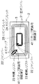
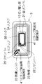
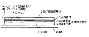
図1は、本実施形態に係るアンテナ回路の構成例の説明図であり、図2は、本実施形態に係るICインレットの構成例の説明図であり、図3は、本実施形態に係るタグ加工したマルチタグ形状例を示す。
次に、第1の実施形態に係るICタグ3の製造方法を以下に説明する。
次に、図3に示す第1の実施形態に係る分離可能なマルチタグである大タグ3A及び小タグ3Bの使用方法例を説明する。
以上のように、本実施形態によれば、大きな回路の内側に小さい回路を同一製造工程で形成することで、従来の回路製造に必要な材料量や作業負担を変えず、複数の回路を同時に作製することができるので、同時に利用される複数のICタグを効率的に製造することができる。
(B−1)上述した実施形態では、回路基材5の一方の面上のみに回路を形成する片側回路による場合を例に挙げて説明したが、回路要素の一部を他面に形成し、回路基材5の両面で回路を作製することを妨げるものではない。例えば、小さいICタグの全部又は一部を回路基材5の他面で形成しても良い。また例えば、ICタグのジャンパー部分を、スルーホールなどを利用して回路基材5の他面に設けるようにしてもよい。なお、ジャンパー部分やICチップ実装用接続端子などの位置は特に限定されるものではない。
続いて、第1の実施形態のICタグ3を作製したので、その製造方法や特性について説明する。
Claims (6)
- 回路基材上に複数個のアンテナ回路部を有し、回路サイズが大きい大アンテナ回路部の内側に、上記大アンテナ回路部より回路サイズが小さい小アンテナ回路部を上記大アンテナ回路部と分離可能なように設けて構成され、上記小アンテナ回路部を分離可能にするための切り離し部を有することを特徴とするアンテナ回路。
- 請求項1に記載のアンテナ回路を構成する上記アンテナ回路部にICチップが実装されて構成されたことを特徴とするICインレット。
- 複数個のタグを有し、回路サイズが大きい大タグの内側に、上記大タグより回路サイズが小さい小タグを上記大タグと分離可能なように設けて構成され、上記小タグを分離可能にするための切り離し部を有することを特徴とするマルチタグ。
- 上記複数個のタグがICタグであることを特徴とする請求項3に記載のマルチタグ。
- 回路サイズが大きい大アンテナ回路部と、その内側に上記大アンテナ回路部より回路サイズが小さい小アンテナ回路部とを回路基材上に形成するアンテナ回路部形成工程と、
上記大アンテナ回路部と上記小アンテナ回路部にICチップを実装するICチップ実装工程と、
上記各アンテナ回路を封止し、所定のタグ加工処理を行うタグ加工工程と、
上記タグ加工工程で形成された小タグを分離可能にするための切り離し部を形成する切り離し部形成工程と
を有することを特徴とするマルチタグ製造方法。 - 作製される大タグと上記小タグとの形成工程を同時に実行することを特徴とする請求項5に記載のマルチタグ製造方法。
Priority Applications (4)
| Application Number | Priority Date | Filing Date | Title |
|---|---|---|---|
| JP2006005179A JP4815217B2 (ja) | 2006-01-12 | 2006-01-12 | アンテナ回路、icインレット、マルチタグ及びマルチタグ製造方法 |
| KR1020060113393A KR101278364B1 (ko) | 2006-01-12 | 2006-11-16 | 안테나 회로, ic 인렛, 멀티 태그 및 멀티 태그 제조 방법 |
| US11/640,935 US7498947B2 (en) | 2006-01-12 | 2006-12-19 | Antenna circuit, IC inlet, multi tag, and method for producing multi tag |
| EP06026602A EP1808800A2 (en) | 2006-01-12 | 2006-12-21 | Antenna circuit, IC inlet, multi tag, and method for producing multi tag |
Applications Claiming Priority (1)
| Application Number | Priority Date | Filing Date | Title |
|---|---|---|---|
| JP2006005179A JP4815217B2 (ja) | 2006-01-12 | 2006-01-12 | アンテナ回路、icインレット、マルチタグ及びマルチタグ製造方法 |
Publications (2)
| Publication Number | Publication Date |
|---|---|
| JP2007188252A JP2007188252A (ja) | 2007-07-26 |
| JP4815217B2 true JP4815217B2 (ja) | 2011-11-16 |
Family
ID=37814483
Family Applications (1)
| Application Number | Title | Priority Date | Filing Date |
|---|---|---|---|
| JP2006005179A Active JP4815217B2 (ja) | 2006-01-12 | 2006-01-12 | アンテナ回路、icインレット、マルチタグ及びマルチタグ製造方法 |
Country Status (4)
| Country | Link |
|---|---|
| US (1) | US7498947B2 (ja) |
| EP (1) | EP1808800A2 (ja) |
| JP (1) | JP4815217B2 (ja) |
| KR (1) | KR101278364B1 (ja) |
Families Citing this family (24)
| Publication number | Priority date | Publication date | Assignee | Title |
|---|---|---|---|---|
| US7665668B2 (en) * | 2006-08-18 | 2010-02-23 | Mastercard International, Inc. | Cut here to destroy indicator |
| JP4784763B2 (ja) * | 2006-12-20 | 2011-10-05 | 株式会社日立プラントテクノロジー | Rfidタグ及びそれを用いた建設現場管理システム並びに管理方法 |
| JP2009064282A (ja) * | 2007-09-07 | 2009-03-26 | Hitachi Ltd | Rfidタグ,rfidシステム,rfidタグの製造装置及びその製造方法 |
| WO2009041497A1 (ja) * | 2007-09-28 | 2009-04-02 | Nec Corporation | ループアンテナ |
| JP2009205669A (ja) * | 2008-01-31 | 2009-09-10 | Semiconductor Energy Lab Co Ltd | 半導体装置 |
| JP5075709B2 (ja) * | 2008-03-28 | 2012-11-21 | 株式会社巴川製紙所 | アンテナ用紙、それを用いたシート状アンテナ及びrfidタグ |
| FI121763B (fi) * | 2008-04-03 | 2011-03-31 | Upm Raflatac Oy | Vahvistinantennin käsittävä transponderi |
| JP5248224B2 (ja) * | 2008-07-09 | 2013-07-31 | リンテック株式会社 | 電子回路及びicタグ |
| TWI373629B (en) * | 2008-08-27 | 2012-10-01 | Mstar Semiconductor Inc | Radio frequency positioning system and method |
| US8188926B2 (en) * | 2008-10-31 | 2012-05-29 | Silicon Laboratories, Inc. | Folded antenna structures for portable devices |
| JP5634084B2 (ja) * | 2010-03-11 | 2014-12-03 | タイコエレクトロニクスジャパン合同会社 | 高周波結合器 |
| WO2011118379A1 (ja) * | 2010-03-24 | 2011-09-29 | 株式会社村田製作所 | Rfidシステム |
| US8991709B2 (en) * | 2010-08-30 | 2015-03-31 | Tagstar Systems Gmbh | Tamper-proof RFID label |
| JP5548897B2 (ja) * | 2012-03-28 | 2014-07-16 | ビッグローブ株式会社 | 携帯端末、情報表示システムおよび情報表示方法 |
| KR101285195B1 (ko) * | 2013-02-07 | 2013-07-10 | 에이큐 주식회사 | 엔에프시용 루프안테나 제조방법 |
| KR101508609B1 (ko) * | 2013-08-30 | 2015-04-07 | 대구대학교 산학협력단 | 에이치에프 유에이치에프 다중대역 알에프아이디 태그 안테나 |
| JP2015170268A (ja) * | 2014-03-10 | 2015-09-28 | 共同印刷株式会社 | Icカードおよびインレット |
| US11177561B2 (en) * | 2014-09-24 | 2021-11-16 | Checkpoint Systems, Inc. | Protected RFID antenna |
| CN105989396A (zh) * | 2015-01-30 | 2016-10-05 | 富泰华工业(深圳)有限公司 | 电子标签 |
| CN106329117A (zh) * | 2016-09-29 | 2017-01-11 | 上海德门电子科技有限公司 | Nfc天线及包含nfc天线的智能装置 |
| JP6787829B2 (ja) * | 2017-03-30 | 2020-11-18 | 日本発條株式会社 | 携帯型無線通信装置、および携帯型無線通信装置を用いる警備システム |
| JP7031322B2 (ja) * | 2018-01-18 | 2022-03-08 | 大日本印刷株式会社 | 熱転写プリンタ、真贋判定システム、印画物の製造方法及び真贋判定方法 |
| KR102162631B1 (ko) | 2018-06-28 | 2020-10-07 | (주)알판트 | 영구 부착형 uhf 대역 알에프아이디 타이어 태그 및 이의 제조 방법 |
| JP7180338B2 (ja) * | 2018-12-05 | 2022-11-30 | 凸版印刷株式会社 | インレイおよびデュアルインターフェースicカード |
Family Cites Families (9)
| Publication number | Priority date | Publication date | Assignee | Title |
|---|---|---|---|---|
| US5574470A (en) * | 1994-09-30 | 1996-11-12 | Palomar Technologies Corporation | Radio frequency identification transponder apparatus and method |
| JPH11328344A (ja) * | 1998-05-08 | 1999-11-30 | Dainippon Printing Co Ltd | 非接触icカード |
| JP4210008B2 (ja) | 1999-10-04 | 2009-01-14 | 大日本印刷株式会社 | 情報処理媒体 |
| JP2002342728A (ja) | 2001-05-16 | 2002-11-29 | Dainippon Printing Co Ltd | ラベル加工用icタグインレットと製造方法 |
| FR2832241B1 (fr) * | 2001-11-09 | 2004-04-09 | Allibert Equipement | Dispositif tracable par un identifiant electronique |
| JP3815337B2 (ja) * | 2002-01-28 | 2006-08-30 | 株式会社デンソーウェーブ | 非接触式icカード |
| US7119693B1 (en) * | 2002-03-13 | 2006-10-10 | Celis Semiconductor Corp. | Integrated circuit with enhanced coupling |
| JP2004213582A (ja) * | 2003-01-09 | 2004-07-29 | Mitsubishi Materials Corp | Rfidタグ及びリーダ/ライタ並びに該タグを備えたrfidシステム |
| US7598876B2 (en) * | 2006-03-21 | 2009-10-06 | Stmicroelectronics Sa | Method for manufacturing a RFID electronic tag |
-
2006
- 2006-01-12 JP JP2006005179A patent/JP4815217B2/ja active Active
- 2006-11-16 KR KR1020060113393A patent/KR101278364B1/ko not_active IP Right Cessation
- 2006-12-19 US US11/640,935 patent/US7498947B2/en not_active Expired - Fee Related
- 2006-12-21 EP EP06026602A patent/EP1808800A2/en not_active Withdrawn
Also Published As
| Publication number | Publication date |
|---|---|
| KR101278364B1 (ko) | 2013-06-25 |
| EP1808800A2 (en) | 2007-07-18 |
| KR20070075258A (ko) | 2007-07-18 |
| US20070159339A1 (en) | 2007-07-12 |
| US7498947B2 (en) | 2009-03-03 |
| JP2007188252A (ja) | 2007-07-26 |
Similar Documents
| Publication | Publication Date | Title |
|---|---|---|
| JP4815217B2 (ja) | アンテナ回路、icインレット、マルチタグ及びマルチタグ製造方法 | |
| JP5169832B2 (ja) | 非接触icタグラベルとその製造方法 | |
| JP4744442B2 (ja) | アンテナ回路、icインレット及びicタグ | |
| JP4599185B2 (ja) | アンテナ回路、及び非接触型icインレットの周波数調整方法 | |
| JP4675184B2 (ja) | Icタグ | |
| JP3953775B2 (ja) | 非接触データキャリア用多面付け基材と多面付けされた非接触データキャリア | |
| JP2004165531A (ja) | 非接触式データキャリア用の両面配線アンテナ回路部材 | |
| JP5049025B2 (ja) | 非接触icタグ | |
| KR101144293B1 (ko) | Ic 태그 | |
| JP4848214B2 (ja) | 非接触icタグ | |
| JP4781871B2 (ja) | 非接触型icラベル | |
| JP5172762B2 (ja) | アンテナ回路、icインレット、icタグ、およびアンテナ回路の容量調整方法 | |
| JP4952030B2 (ja) | 非接触型データキャリア装置とこれを配設したデータキャリア装置配設部材 | |
| JP5035501B2 (ja) | 非接触型データキャリア装置 | |
| JP4839668B2 (ja) | 非接触icタグの製造方法 | |
| JP2008097525A (ja) | Icタグシート | |
| JP4580944B2 (ja) | 非接触データキャリアとその製造方法 | |
| JP2005284813A (ja) | Rf−idメディアの製造方法 | |
| JP2013210948A (ja) | 金属体貼付用データキャリア、データキャリアの貼付方法および無線通信方法 | |
| JP2014010473A (ja) | アンテナ回路部材、icインレット、icチップの保護方法、およびアンテナ回路部材の製造方法 | |
| JP2007207122A (ja) | 非接触型データキャリア装置とこれを配設したデータキャリア装置配設部材、および、これらの製造方法 | |
| JP2013229012A (ja) | 金属貼付用データキャリア及び無線通信方法 | |
| KR20090019280A (ko) | 원칩과 안테나의 접속방법 | |
| JP2007079632A (ja) | 非接触icカード及びその非接触icカード用の平板状カード基板 |
Legal Events
| Date | Code | Title | Description |
|---|---|---|---|
| A621 | Written request for application examination |
Free format text: JAPANESE INTERMEDIATE CODE: A621 Effective date: 20080918 |
|
| A977 | Report on retrieval |
Free format text: JAPANESE INTERMEDIATE CODE: A971007 Effective date: 20110629 |
|
| A131 | Notification of reasons for refusal |
Free format text: JAPANESE INTERMEDIATE CODE: A131 Effective date: 20110712 |
|
| A521 | Request for written amendment filed |
Free format text: JAPANESE INTERMEDIATE CODE: A523 Effective date: 20110804 |
|
| TRDD | Decision of grant or rejection written | ||
| A01 | Written decision to grant a patent or to grant a registration (utility model) |
Free format text: JAPANESE INTERMEDIATE CODE: A01 Effective date: 20110823 |
|
| A01 | Written decision to grant a patent or to grant a registration (utility model) |
Free format text: JAPANESE INTERMEDIATE CODE: A01 |
|
| A61 | First payment of annual fees (during grant procedure) |
Free format text: JAPANESE INTERMEDIATE CODE: A61 Effective date: 20110829 |
|
| R150 | Certificate of patent or registration of utility model |
Ref document number: 4815217 Country of ref document: JP Free format text: JAPANESE INTERMEDIATE CODE: R150 Free format text: JAPANESE INTERMEDIATE CODE: R150 |
|
| FPAY | Renewal fee payment (event date is renewal date of database) |
Free format text: PAYMENT UNTIL: 20170902 Year of fee payment: 6 |
|
| R250 | Receipt of annual fees |
Free format text: JAPANESE INTERMEDIATE CODE: R250 |
|
| R250 | Receipt of annual fees |
Free format text: JAPANESE INTERMEDIATE CODE: R250 |
|
| R250 | Receipt of annual fees |
Free format text: JAPANESE INTERMEDIATE CODE: R250 |
|
| R250 | Receipt of annual fees |
Free format text: JAPANESE INTERMEDIATE CODE: R250 |
|
| R250 | Receipt of annual fees |
Free format text: JAPANESE INTERMEDIATE CODE: R250 |
|
| R250 | Receipt of annual fees |
Free format text: JAPANESE INTERMEDIATE CODE: R250 |
|
| R250 | Receipt of annual fees |
Free format text: JAPANESE INTERMEDIATE CODE: R250 |