JP4557577B2 - チャージポンプ回路 - Google Patents
チャージポンプ回路 Download PDFInfo
- Publication number
- JP4557577B2 JP4557577B2 JP2004092639A JP2004092639A JP4557577B2 JP 4557577 B2 JP4557577 B2 JP 4557577B2 JP 2004092639 A JP2004092639 A JP 2004092639A JP 2004092639 A JP2004092639 A JP 2004092639A JP 4557577 B2 JP4557577 B2 JP 4557577B2
- Authority
- JP
- Japan
- Prior art keywords
- mos transistor
- charge transfer
- transfer mos
- clock
- voltage
- Prior art date
- Legal status (The legal status is an assumption and is not a legal conclusion. Google has not performed a legal analysis and makes no representation as to the accuracy of the status listed.)
- Expired - Fee Related
Links
Images


Classifications
-
- H—ELECTRICITY
- H02—GENERATION; CONVERSION OR DISTRIBUTION OF ELECTRIC POWER
- H02M—APPARATUS FOR CONVERSION BETWEEN AC AND AC, BETWEEN AC AND DC, OR BETWEEN DC AND DC, AND FOR USE WITH MAINS OR SIMILAR POWER SUPPLY SYSTEMS; CONVERSION OF DC OR AC INPUT POWER INTO SURGE OUTPUT POWER; CONTROL OR REGULATION THEREOF
- H02M3/00—Conversion of dc power input into dc power output
- H02M3/02—Conversion of dc power input into dc power output without intermediate conversion into ac
- H02M3/04—Conversion of dc power input into dc power output without intermediate conversion into ac by static converters
- H02M3/06—Conversion of dc power input into dc power output without intermediate conversion into ac by static converters using resistors or capacitors, e.g. potential divider
- H02M3/07—Conversion of dc power input into dc power output without intermediate conversion into ac by static converters using resistors or capacitors, e.g. potential divider using capacitors charged and discharged alternately by semiconductor devices with control electrode, e.g. charge pumps
- H02M3/073—Charge pumps of the Schenkel-type
-
- G—PHYSICS
- G11—INFORMATION STORAGE
- G11C—STATIC STORES
- G11C5/00—Details of stores covered by group G11C11/00
- G11C5/14—Power supply arrangements, e.g. power down, chip selection or deselection, layout of wirings or power grids, or multiple supply levels
-
- H—ELECTRICITY
- H02—GENERATION; CONVERSION OR DISTRIBUTION OF ELECTRIC POWER
- H02M—APPARATUS FOR CONVERSION BETWEEN AC AND AC, BETWEEN AC AND DC, OR BETWEEN DC AND DC, AND FOR USE WITH MAINS OR SIMILAR POWER SUPPLY SYSTEMS; CONVERSION OF DC OR AC INPUT POWER INTO SURGE OUTPUT POWER; CONTROL OR REGULATION THEREOF
- H02M3/00—Conversion of dc power input into dc power output
- H02M3/02—Conversion of dc power input into dc power output without intermediate conversion into ac
- H02M3/04—Conversion of dc power input into dc power output without intermediate conversion into ac by static converters
- H02M3/06—Conversion of dc power input into dc power output without intermediate conversion into ac by static converters using resistors or capacitors, e.g. potential divider
- H02M3/07—Conversion of dc power input into dc power output without intermediate conversion into ac by static converters using resistors or capacitors, e.g. potential divider using capacitors charged and discharged alternately by semiconductor devices with control electrode, e.g. charge pumps
- H02M3/073—Charge pumps of the Schenkel-type
- H02M3/075—Charge pumps of the Schenkel-type including a plurality of stages and two sets of clock signals, one set for the odd and one set for the even numbered stages
-
- H—ELECTRICITY
- H02—GENERATION; CONVERSION OR DISTRIBUTION OF ELECTRIC POWER
- H02M—APPARATUS FOR CONVERSION BETWEEN AC AND AC, BETWEEN AC AND DC, OR BETWEEN DC AND DC, AND FOR USE WITH MAINS OR SIMILAR POWER SUPPLY SYSTEMS; CONVERSION OF DC OR AC INPUT POWER INTO SURGE OUTPUT POWER; CONTROL OR REGULATION THEREOF
- H02M3/00—Conversion of dc power input into dc power output
- H02M3/02—Conversion of dc power input into dc power output without intermediate conversion into ac
- H02M3/04—Conversion of dc power input into dc power output without intermediate conversion into ac by static converters
- H02M3/06—Conversion of dc power input into dc power output without intermediate conversion into ac by static converters using resistors or capacitors, e.g. potential divider
- H02M3/07—Conversion of dc power input into dc power output without intermediate conversion into ac by static converters using resistors or capacitors, e.g. potential divider using capacitors charged and discharged alternately by semiconductor devices with control electrode, e.g. charge pumps
- H02M3/073—Charge pumps of the Schenkel-type
- H02M3/077—Charge pumps of the Schenkel-type with parallel connected charge pump stages
-
- H—ELECTRICITY
- H04—ELECTRIC COMMUNICATION TECHNIQUE
- H04R—LOUDSPEAKERS, MICROPHONES, GRAMOPHONE PICK-UPS OR LIKE ACOUSTIC ELECTROMECHANICAL TRANSDUCERS; DEAF-AID SETS; PUBLIC ADDRESS SYSTEMS
- H04R19/00—Electrostatic transducers
- H04R19/04—Microphones
Description
Vout=(N+1)(Vdd−Vd)
なお、先行技術文献として以下の特許文献1、非特許文献1がある。
前記第1の電荷転送用スイッチング素子と前記第2の電荷転送用スイッチング素子の接続点に一方の端子が接続された第1のコンデンサと、
直列に接続された第3及び第4の電荷転送用スイッチング素子と、
前記第3の電荷転送用スイッチング素子と前記第4の電荷転送用スイッチング素子の接続点に一方の端子が接続された第2のコンデンサと、
前記第1のコンデンサの他方の端子と前記第2のコンデンサの他方に端子に相補的なクロックを供給するクロックドライバーと、
前記第1及び第3の電荷転送用スイッチング素子が接続された入力端子に入力電圧を供給する電圧源と、前記第1乃至第4の電荷転送用スイッチング素子を全てオフさせた状態で前記クロックドライバーのクロックの電圧レベルを反転させ、その後、前記第2及び第3の電荷転送用スイッチング素子をオンさせ、その後、前記第1乃至第4の電荷転送用スイッチング素子を全てオフさせた状態で前記クロックドライバーのクロックの電圧レベルを更に反転させ、その後、前記第1及び第4の電荷転送用スイッチング素子をオンさせるように制御する制御回路と、を備え、前記第2及び第4の電荷転送用スイッチング素子が接続された出力端子から前記入力電圧が昇圧された出力電圧を得ることを特徴とするものである。
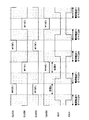
第1のクロックCLK(B)をロウからハイへ変化させると、M11,M17のゲート電圧はVin+Vddになり、M11及びM17がオンする。M11がオンすることで第1のポンピングコンデンサCAが充電される。また、M17がオンすることでM13のゲート電圧は入力電圧Vinになるので、M13はオフする。
M1 第1の電荷転送用MOSトランジスタ
M2 第2の電荷転送用MOSトランジスタ
M3 第3の電荷転送用MOSトランジスタ
M4 第4の電荷転送用MOSトランジスタ
C1 第1のポンピングコンデンサ
C2 第2のポンピングコンデンサ
M11 第1の電荷転送用MOSトランジスタ
M12 第2の電荷転送用MOSトランジスタ
M13 第3の電荷転送用MOSトランジスタ
M14 第4の電荷転送用MOSトランジスタ
CA 第1のポンピングコンデンサ
CB 第2のポンピングコンデンサ
M15 第1のバイアス用MOSトランジスタ
M16 第2のバイアス用MOSトランジスタ
M17 第3のバイアス用MOSトランジスタ
M18 第4のバイアス用MOSトランジスタ
C11 第1のカップリングコンデンサ
C12 第2のカップリングコンデンサ
C13 第3のカップリングコンデンサ
C14 第4のカップリングコンデンサ
Claims (6)
- 直列に接続された第1及び第2の電荷転送用MOSトランジスタと、
前記第1の電荷転送用MOSトランジスタと前記第2の電荷転送用MOSトランジスタの接続点に一方の端子が接続された第1のコンデンサと、
直列に接続された第3及び第4の電荷転送用MOSトランジスタと、
前記第3の電荷転送用MOSトランジスタと前記第4の電荷転送用MOSトランジスタの接続点に一方の端子が接続された第2のコンデンサと、
前記第1のコンデンサの他方の端子と前記第2のコンデンサの他方に端子に相補的なクロックを供給するクロックドライバーと、
前記第1及び第3の電荷転送用MOSトランジスタが接続された入力端子に入力電圧を供給する電圧源と、
前記第1乃至第4の電荷転送用MOSトランジスタを全てオフさせた状態で前記クロックドライバーのクロックの電圧レベルを反転させ、その後、前記第2及び第3の電荷転送用MOSトランジスタをオンさせ、その後、前記第1乃至第4の電荷転送用MOSトランジスタを全てオフさせた状態で前記クロックドライバーのクロックの電圧レベルを更に反転させ、その後、前記第1及び第4の電荷転送用MOSトランジスタをオンさせるように制御する制御回路と、
前記第2及び第4の電荷転送用MOSトランジスタが接続された出力端子から前記入力電圧が昇圧された出力電圧を出力する出力回路と、
前記第1の電荷転送用MOSトランジスタ及び前記第3の電荷転送用MOSトランジスタのゲートの電圧の初期値が所定値以上にならないように電圧設定する初期電圧設定回路と、を備え、
前記制御回路は、第1の電荷転送用MOSトランジスタのゲートに第1の結合コンデンサを介して第1のクロックを供給する第1のクロック供給手段と、
前記第1の電荷転送用MOSトランジスタのゲートに前記入力電圧を供給する第1のバイアス用MOSトランジスタと、
第3の電荷転送用MOSトランジスタのゲートに第3の結合コンデンサを介して第3のクロックを供給する第3のクロック供給手段と、
前記第3の電荷転送用MOSトランジスタのゲートに前記入力電圧を供給する第3のバイアス用MOSトランジスタと、を有し、前記第1のクロックが第1のレベルから第2のレベルに変化すると前記第1の電荷転送用MOSトランジスタ及び前記第3のバイアス用MOSトランジスタがオンし、前記第3の電荷転送用MOSトランジスタがオフし、次に、前記第3のクロックが第1のレベルから第2のレベルに変化すると前記第3の電荷転送用MOSトランジスタ及び前記第1のバイアス用MOSトランジスタがオンし、前記第1の電荷転送用MOSトランジスタがオフするように制御することを特徴とするチャージポンプ回路。 - 前記初期電圧設定回路は、前記第1の電荷転送用MOSトランジスタのゲート及び前記第2の電荷転送用MOSトランジスタのゲートと前記出力端子との間に設けられた一対のダイオード素子で構成されることを特徴とする請求項1に記載のチャージポンプ回路。
- 前記制御回路は、第2の電荷転送用MOSトランジスタのゲートに第2の結合コンデンサを介して第2のクロックを供給する第2のクロック供給手段と、
前記第2の電荷転送用MOSトランジスタのゲートに前記出力電圧を供給する第2のバイ
アス用MOSトランジスタと、
第4の電荷転送用MOSトランジスタのゲートに第4の結合コンデンサを介して第4のクロックを供給する第4のクロック供給手段と、
前記第4の電荷転送用MOSトランジスタのゲートに前記出力電圧を供給する第4のバイアス用MOSトランジスタと、を有し、
前記第2のクロックが第1のレベルから第2のレベルに変化すると前記第2の電荷転送用MOSトランジスタ及び前記第4のバイアス用MOSトランジスタがオンし、前記第4の電荷転送用MOSトランジスタがオフし、次に、前記第4のクロックが第1のレベルから第2のレベルに変化すると前記第4の電荷転送用MOSトランジスタ及び前記第2のバイアス用MOSトランジスタがオンし、前記第2の電荷転送用MOSトランジスタがオフするように制御することを特徴とする請求項2に記載のチャージポンプ回路。 - 前記第2の電荷転送用MOSトランジスタ及び前記第4の電荷転送用MOSトランジスタのゲートの電圧の初期値が所定値以下にならないように電圧設定する初期電圧設定回路を設けたことを特徴とする請求項3に記載のチャージポンプ回路。
- 前記初期電圧設定回路は、前記第3の電荷転送用MOSトランジスタのゲート及び前記第4の電荷転送用MOSトランジスタのゲートと前記入力端子との間に設けられた一対のダイオード素子で構成されることを特徴とする請求項4に記載のチャージポンプ回路。
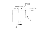
- 前記出力電圧をコンデンサマイクの電源電圧として用いることを特徴とする請求項5に記載のチャージポンプ回路。
Priority Applications (5)
| Application Number | Priority Date | Filing Date | Title |
|---|---|---|---|
| JP2004092639A JP4557577B2 (ja) | 2004-03-26 | 2004-03-26 | チャージポンプ回路 |
| TW094108303A TWI264872B (en) | 2004-03-26 | 2005-03-18 | Charge pump circuit |
| KR1020050024410A KR100684244B1 (ko) | 2004-03-26 | 2005-03-24 | 차지 펌프 회로 |
| US11/089,031 US7208996B2 (en) | 2004-03-26 | 2005-03-25 | Charge pump circuit |
| CN2005100624379A CN1674444B (zh) | 2004-03-26 | 2005-03-28 | 电荷泵电路 |
Applications Claiming Priority (1)
| Application Number | Priority Date | Filing Date | Title |
|---|---|---|---|
| JP2004092639A JP4557577B2 (ja) | 2004-03-26 | 2004-03-26 | チャージポンプ回路 |
Publications (2)
| Publication Number | Publication Date |
|---|---|
| JP2005278378A JP2005278378A (ja) | 2005-10-06 |
| JP4557577B2 true JP4557577B2 (ja) | 2010-10-06 |
Family
ID=34989841
Family Applications (1)
| Application Number | Title | Priority Date | Filing Date |
|---|---|---|---|
| JP2004092639A Expired - Fee Related JP4557577B2 (ja) | 2004-03-26 | 2004-03-26 | チャージポンプ回路 |
Country Status (5)
| Country | Link |
|---|---|
| US (1) | US7208996B2 (ja) |
| JP (1) | JP4557577B2 (ja) |
| KR (1) | KR100684244B1 (ja) |
| CN (1) | CN1674444B (ja) |
| TW (1) | TWI264872B (ja) |
Families Citing this family (49)
| Publication number | Priority date | Publication date | Assignee | Title |
|---|---|---|---|---|
| EP1881589A1 (en) * | 2006-07-19 | 2008-01-23 | STMicroelectronics S.r.l. | Charge pump circuit |
| JP4642794B2 (ja) * | 2007-03-27 | 2011-03-02 | エプソンイメージングデバイス株式会社 | 電源回路及び表示装置 |
| US8044705B2 (en) * | 2007-08-28 | 2011-10-25 | Sandisk Technologies Inc. | Bottom plate regulation of charge pumps |
| US20090066407A1 (en) * | 2007-09-12 | 2009-03-12 | Rochester Institute Of Technology | Charge pump systems and methods thereof |
| US7595683B1 (en) * | 2007-11-15 | 2009-09-29 | Fairchild Semiconductor Corporation | Low-input-voltage charge pump |
| JP5096198B2 (ja) * | 2008-03-18 | 2012-12-12 | 株式会社リコー | 電圧発生回路 |
| JP5804943B2 (ja) * | 2008-05-05 | 2015-11-04 | エプコス ピーティーイー リミテッド | 高速で精密な電荷ポンプ |
| US7969235B2 (en) * | 2008-06-09 | 2011-06-28 | Sandisk Corporation | Self-adaptive multi-stage charge pump |
| US8710907B2 (en) * | 2008-06-24 | 2014-04-29 | Sandisk Technologies Inc. | Clock generator circuit for a charge pump |
| KR101447917B1 (ko) | 2008-08-01 | 2014-10-14 | 삼성전자주식회사 | 차지 펌핑 동작을 수행하는 반도체 장치 |
| JP5180793B2 (ja) * | 2008-11-28 | 2013-04-10 | キヤノン株式会社 | クロック生成回路、集積回路及び撮像センサ |
| US8076968B1 (en) | 2009-03-09 | 2011-12-13 | Fairchild Semiconductor Corporation | Low-input-voltage charge pump |
| US8154333B2 (en) * | 2009-04-01 | 2012-04-10 | Taiwan Semiconductor Manufacturing Company, Ltd. | Charge pump circuits, systems, and operational methods thereof |
| US7973592B2 (en) * | 2009-07-21 | 2011-07-05 | Sandisk Corporation | Charge pump with current based regulation |
| US8339183B2 (en) * | 2009-07-24 | 2012-12-25 | Sandisk Technologies Inc. | Charge pump with reduced energy consumption through charge sharing and clock boosting suitable for high voltage word line in flash memories |
| US20110133820A1 (en) * | 2009-12-09 | 2011-06-09 | Feng Pan | Multi-Stage Charge Pump with Variable Number of Boosting Stages |
| US20110148509A1 (en) * | 2009-12-17 | 2011-06-23 | Feng Pan | Techniques to Reduce Charge Pump Overshoot |
| CN101807915B (zh) * | 2010-04-15 | 2012-05-30 | 复旦大学 | 应用于整数分频锁相环路中的鉴频鉴相器和电荷泵电路 |
| JP2012115046A (ja) * | 2010-11-25 | 2012-06-14 | Renesas Electronics Corp | チャージポンプ回路 |
| US8294509B2 (en) | 2010-12-20 | 2012-10-23 | Sandisk Technologies Inc. | Charge pump systems with reduction in inefficiencies due to charge sharing between capacitances |
| US8339185B2 (en) | 2010-12-20 | 2012-12-25 | Sandisk 3D Llc | Charge pump system that dynamically selects number of active stages |
| US8699247B2 (en) | 2011-09-09 | 2014-04-15 | Sandisk Technologies Inc. | Charge pump system dynamically reconfigurable for read and program |
| US8514628B2 (en) | 2011-09-22 | 2013-08-20 | Sandisk Technologies Inc. | Dynamic switching approach to reduce area and power consumption of high voltage charge pumps |
| US8400212B1 (en) | 2011-09-22 | 2013-03-19 | Sandisk Technologies Inc. | High voltage charge pump regulation system with fine step adjustment |
| US8710909B2 (en) | 2012-09-14 | 2014-04-29 | Sandisk Technologies Inc. | Circuits for prevention of reverse leakage in Vth-cancellation charge pumps |
| WO2014100184A1 (en) * | 2012-12-19 | 2014-06-26 | Knowles Electronics, Llc | Apparatus and method for high voltage i/o electro-static discharge protection |
| US8836412B2 (en) | 2013-02-11 | 2014-09-16 | Sandisk 3D Llc | Charge pump with a power-controlled clock buffer to reduce power consumption and output voltage ripple |
| US8981835B2 (en) | 2013-06-18 | 2015-03-17 | Sandisk Technologies Inc. | Efficient voltage doubler |
| US9024680B2 (en) | 2013-06-24 | 2015-05-05 | Sandisk Technologies Inc. | Efficiency for charge pumps with low supply voltages |
| US9077238B2 (en) | 2013-06-25 | 2015-07-07 | SanDisk Technologies, Inc. | Capacitive regulation of charge pumps without refresh operation interruption |
| US9007046B2 (en) | 2013-06-27 | 2015-04-14 | Sandisk Technologies Inc. | Efficient high voltage bias regulation circuit |
| US9083231B2 (en) | 2013-09-30 | 2015-07-14 | Sandisk Technologies Inc. | Amplitude modulation for pass gate to improve charge pump efficiency |
| US9154027B2 (en) | 2013-12-09 | 2015-10-06 | Sandisk Technologies Inc. | Dynamic load matching charge pump for reduced current consumption |
| US9531262B2 (en) * | 2014-01-03 | 2016-12-27 | Analog Devices Global | Charge pump |
| DE102014115433A1 (de) * | 2014-10-23 | 2016-05-12 | Infineon Technologies Ag | Ladungspumpe |
| US11611276B2 (en) | 2014-12-04 | 2023-03-21 | Taiwan Semiconductor Manufacturing Company, Ltd. | Charge pump circuit |
| US9491151B2 (en) | 2015-01-07 | 2016-11-08 | Ememory Technology Inc. | Memory apparatus, charge pump circuit and voltage pumping method thereof |
| US9831860B2 (en) * | 2015-03-16 | 2017-11-28 | Taiwan Semiconductor Manufacturing Company, Ltd. | Clock generation circuit |
| US9917507B2 (en) | 2015-05-28 | 2018-03-13 | Sandisk Technologies Llc | Dynamic clock period modulation scheme for variable charge pump load currents |
| US9602921B2 (en) | 2015-06-24 | 2017-03-21 | Robert Bosch Gmbh | Independently charge pumps for differential microphone |
| US9647536B2 (en) | 2015-07-28 | 2017-05-09 | Sandisk Technologies Llc | High voltage generation using low voltage devices |
| US9520776B1 (en) | 2015-09-18 | 2016-12-13 | Sandisk Technologies Llc | Selective body bias for charge pump transfer switches |
| CN105720813A (zh) * | 2016-04-22 | 2016-06-29 | 中国科学院微电子研究所 | 一种电荷泵电路 |
| CN105743328B (zh) * | 2016-04-28 | 2019-02-01 | 广东合微集成电路技术有限公司 | 一种晶体管、电荷泵组件以及电荷泵 |
| CN107181403A (zh) * | 2017-05-31 | 2017-09-19 | 成都锐成芯微科技股份有限公司 | 差分电荷泵电路 |
| US10461635B1 (en) * | 2018-05-15 | 2019-10-29 | Analog Devices Global Unlimited Company | Low VIN high efficiency chargepump |
| JP6783879B2 (ja) * | 2019-01-29 | 2020-11-11 | ウィンボンド エレクトロニクス コーポレーション | チャージポンプ回路 |
| EP3819905A1 (en) * | 2019-11-05 | 2021-05-12 | EM Microelectronic-Marin SA | Gate controller for a change pump converter |
| CN114204804B (zh) * | 2020-09-17 | 2024-04-16 | 圣邦微电子(北京)股份有限公司 | 一种电荷泵电路 |
Citations (1)
| Publication number | Priority date | Publication date | Assignee | Title |
|---|---|---|---|---|
| JP2003100077A (ja) * | 2001-09-27 | 2003-04-04 | Sony Corp | 昇圧電位発生回路 |
Family Cites Families (10)
| Publication number | Priority date | Publication date | Assignee | Title |
|---|---|---|---|---|
| KR100243004B1 (ko) * | 1997-02-27 | 2000-03-02 | 김영환 | 부트스트랩 챠지 펌프회로 |
| JP3385960B2 (ja) * | 1998-03-16 | 2003-03-10 | 日本電気株式会社 | 負電圧チャージポンプ回路 |
| JP4026947B2 (ja) * | 1998-08-24 | 2007-12-26 | 株式会社ルネサステクノロジ | 昇圧回路 |
| US6429723B1 (en) * | 1999-11-18 | 2002-08-06 | Texas Instruments Incorporated | Integrated circuit with charge pump and method |
| JP2001211637A (ja) | 2000-01-21 | 2001-08-03 | Haruo Kobayashi | チャージポンプ回路 |
| JP2002208290A (ja) * | 2001-01-09 | 2002-07-26 | Mitsubishi Electric Corp | チャージポンプ回路およびこれを用いた不揮発性メモリの動作方法 |
| JP2003033006A (ja) | 2001-07-18 | 2003-01-31 | Sanyo Electric Co Ltd | チャージポンプ回路 |
| ITMI20012789A1 (it) * | 2001-12-21 | 2003-06-21 | St Microelectronics Srl | Sistema a pompa di carica |
| JP2003284325A (ja) | 2002-03-20 | 2003-10-03 | Sanyo Electric Co Ltd | チャージポンプ回路およびチャージポンプ回路を備えた表示装置 |
| FR2864271B1 (fr) * | 2003-12-19 | 2006-03-03 | Atmel Corp | Circuit de pompe a charge a rendement eleve, a faible cout |
-
2004
- 2004-03-26 JP JP2004092639A patent/JP4557577B2/ja not_active Expired - Fee Related
-
2005
- 2005-03-18 TW TW094108303A patent/TWI264872B/zh not_active IP Right Cessation
- 2005-03-24 KR KR1020050024410A patent/KR100684244B1/ko not_active IP Right Cessation
- 2005-03-25 US US11/089,031 patent/US7208996B2/en active Active
- 2005-03-28 CN CN2005100624379A patent/CN1674444B/zh active Active
Patent Citations (1)
| Publication number | Priority date | Publication date | Assignee | Title |
|---|---|---|---|---|
| JP2003100077A (ja) * | 2001-09-27 | 2003-04-04 | Sony Corp | 昇圧電位発生回路 |
Also Published As
| Publication number | Publication date |
|---|---|
| CN1674444B (zh) | 2010-05-12 |
| CN1674444A (zh) | 2005-09-28 |
| KR20060044671A (ko) | 2006-05-16 |
| KR100684244B1 (ko) | 2007-02-20 |
| TW200603540A (en) | 2006-01-16 |
| JP2005278378A (ja) | 2005-10-06 |
| US7208996B2 (en) | 2007-04-24 |
| US20050213781A1 (en) | 2005-09-29 |
| TWI264872B (en) | 2006-10-21 |
Similar Documents
| Publication | Publication Date | Title |
|---|---|---|
| JP4557577B2 (ja) | チャージポンプ回路 | |
| TW578377B (en) | Charge-pump circuit and method for controlling the same | |
| JPH10199281A (ja) | 昇圧回路及びこれを備えたicカード | |
| KR20050072145A (ko) | 승압 회로 | |
| JP5566568B2 (ja) | 電源電圧発生回路 | |
| JPH09198887A (ja) | 高電圧発生回路 | |
| JP4299857B2 (ja) | 昇圧型チャージポンプ回路 | |
| KR20070032927A (ko) | 차지 펌프식 승압 회로를 갖는 반도체 장치 | |
| US8421522B2 (en) | High voltage generator and method of generating high voltage | |
| JP2015142449A (ja) | チャージポンプ回路 | |
| US7683699B2 (en) | Charge pump | |
| KR100403528B1 (ko) | 차지 펌프 회로 및 그 제어 방법 | |
| US11114937B2 (en) | Charge pump circuit | |
| EP1601091B1 (en) | Control circuit for a polarity inverting buck-boost DC-DC converter | |
| JP2005117830A (ja) | チャージポンプ回路 | |
| JP5056427B2 (ja) | チャージポンプ回路 | |
| JP2005044203A (ja) | 電源回路 | |
| KR100349349B1 (ko) | 승압 전압 발생기 | |
| CN111490676B (zh) | 电荷泵电路、半导体装置以及半导体存储装置 | |
| US10756713B2 (en) | Clock signal boost circuit | |
| JP2005102375A (ja) | チャージポンプ回路 | |
| JP2002058237A (ja) | チャージポンプ回路及びその制御方法 | |
| JP4634154B2 (ja) | 昇圧回路 | |
| KR20100035734A (ko) | 차지 펌프 회로 | |
| JP2011004535A (ja) | 昇圧回路 |
Legal Events
| Date | Code | Title | Description |
|---|---|---|---|
| A621 | Written request for application examination |
Free format text: JAPANESE INTERMEDIATE CODE: A621 Effective date: 20070208 |
|
| A977 | Report on retrieval |
Free format text: JAPANESE INTERMEDIATE CODE: A971007 Effective date: 20090924 |
|
| A131 | Notification of reasons for refusal |
Free format text: JAPANESE INTERMEDIATE CODE: A131 Effective date: 20091014 |
|
| A521 | Written amendment |
Free format text: JAPANESE INTERMEDIATE CODE: A523 Effective date: 20091207 |
|
| A131 | Notification of reasons for refusal |
Free format text: JAPANESE INTERMEDIATE CODE: A131 Effective date: 20100223 |
|
| A521 | Written amendment |
Free format text: JAPANESE INTERMEDIATE CODE: A523 Effective date: 20100412 |
|
| TRDD | Decision of grant or rejection written | ||
| A01 | Written decision to grant a patent or to grant a registration (utility model) |
Free format text: JAPANESE INTERMEDIATE CODE: A01 Effective date: 20100621 |
|
| A01 | Written decision to grant a patent or to grant a registration (utility model) |
Free format text: JAPANESE INTERMEDIATE CODE: A01 |
|
| A61 | First payment of annual fees (during grant procedure) |
Free format text: JAPANESE INTERMEDIATE CODE: A61 Effective date: 20100720 |
|
| FPAY | Renewal fee payment (event date is renewal date of database) |
Free format text: PAYMENT UNTIL: 20130730 Year of fee payment: 3 |
|
| R250 | Receipt of annual fees |
Free format text: JAPANESE INTERMEDIATE CODE: R250 |
|
| LAPS | Cancellation because of no payment of annual fees |