JP4458329B2 - 露光装置及びデバイス製造方法 - Google Patents
露光装置及びデバイス製造方法 Download PDFInfo
- Publication number
- JP4458329B2 JP4458329B2 JP2003434549A JP2003434549A JP4458329B2 JP 4458329 B2 JP4458329 B2 JP 4458329B2 JP 2003434549 A JP2003434549 A JP 2003434549A JP 2003434549 A JP2003434549 A JP 2003434549A JP 4458329 B2 JP4458329 B2 JP 4458329B2
- Authority
- JP
- Japan
- Prior art keywords
- exposure
- slit
- wafer
- exposure apparatus
- guide mechanism
- Prior art date
- Legal status (The legal status is an assumption and is not a legal conclusion. Google has not performed a legal analysis and makes no representation as to the accuracy of the status listed.)
- Expired - Fee Related
Links
Images


Classifications
-
- G—PHYSICS
- G03—PHOTOGRAPHY; CINEMATOGRAPHY; ANALOGOUS TECHNIQUES USING WAVES OTHER THAN OPTICAL WAVES; ELECTROGRAPHY; HOLOGRAPHY
- G03F—PHOTOMECHANICAL PRODUCTION OF TEXTURED OR PATTERNED SURFACES, e.g. FOR PRINTING, FOR PROCESSING OF SEMICONDUCTOR DEVICES; MATERIALS THEREFOR; ORIGINALS THEREFOR; APPARATUS SPECIALLY ADAPTED THEREFOR
- G03F7/00—Photomechanical, e.g. photolithographic, production of textured or patterned surfaces, e.g. printing surfaces; Materials therefor, e.g. comprising photoresists; Apparatus specially adapted therefor
- G03F7/70—Microphotolithographic exposure; Apparatus therefor
- G03F7/70058—Mask illumination systems
- G03F7/70083—Non-homogeneous intensity distribution in the mask plane
-
- G—PHYSICS
- G03—PHOTOGRAPHY; CINEMATOGRAPHY; ANALOGOUS TECHNIQUES USING WAVES OTHER THAN OPTICAL WAVES; ELECTROGRAPHY; HOLOGRAPHY
- G03F—PHOTOMECHANICAL PRODUCTION OF TEXTURED OR PATTERNED SURFACES, e.g. FOR PRINTING, FOR PROCESSING OF SEMICONDUCTOR DEVICES; MATERIALS THEREFOR; ORIGINALS THEREFOR; APPARATUS SPECIALLY ADAPTED THEREFOR
- G03F7/00—Photomechanical, e.g. photolithographic, production of textured or patterned surfaces, e.g. printing surfaces; Materials therefor, e.g. comprising photoresists; Apparatus specially adapted therefor
- G03F7/70—Microphotolithographic exposure; Apparatus therefor
- G03F7/70058—Mask illumination systems
- G03F7/70066—Size and form of the illuminated area in the mask plane, e.g. reticle masking blades or blinds
-
- G—PHYSICS
- G03—PHOTOGRAPHY; CINEMATOGRAPHY; ANALOGOUS TECHNIQUES USING WAVES OTHER THAN OPTICAL WAVES; ELECTROGRAPHY; HOLOGRAPHY
- G03F—PHOTOMECHANICAL PRODUCTION OF TEXTURED OR PATTERNED SURFACES, e.g. FOR PRINTING, FOR PROCESSING OF SEMICONDUCTOR DEVICES; MATERIALS THEREFOR; ORIGINALS THEREFOR; APPARATUS SPECIALLY ADAPTED THEREFOR
- G03F7/00—Photomechanical, e.g. photolithographic, production of textured or patterned surfaces, e.g. printing surfaces; Materials therefor, e.g. comprising photoresists; Apparatus specially adapted therefor
- G03F7/70—Microphotolithographic exposure; Apparatus therefor
- G03F7/70483—Information management; Active and passive control; Testing; Wafer monitoring, e.g. pattern monitoring
- G03F7/7055—Exposure light control in all parts of the microlithographic apparatus, e.g. pulse length control or light interruption
- G03F7/70558—Dose control, i.e. achievement of a desired dose
Landscapes
- Physics & Mathematics (AREA)
- General Physics & Mathematics (AREA)
- Exposure And Positioning Against Photoresist Photosensitive Materials (AREA)
- Exposure Of Semiconductors, Excluding Electron Or Ion Beam Exposure (AREA)
Description
Pr=Qw×Lw÷Vw・・・(式1)
と表現されるので、
Vw=Qw×Lw÷Pr・・・(式2)
と書き換えられ、レジストの感度Prを2,000J/m2、ウエハ25面上に露光される単位当たりの露光量(以下ウエハ面照度と呼ぶ)Qwを30,000W/m2、スキャン方向の開口幅Lwを10mmとすると、ウエハ25のスキャン速度Vwは0.15m/secとなる。しかし、ここで光源1の出力が低下してウエハ面照度Qwが20,000W/m2まで低下すると、スキャン速度Vwは0.10m/secに低下する。このことは露光に要する時間が長くなることを意味し、生産性の低下を招く結果となる。
OplusEの1993年2月号の96〜99頁
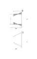
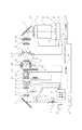
前記照明光学系は、前記被照明面と共役な位置の近傍に配置された、開口幅が可変な開口可変機構を有し、
該開口可変機構が、一枚の遮光板と、該一枚の遮光板の複数箇所に対して力を加えるために、前記マスクと前記基板との相対移動の方向に対応する方向の駆動軸を有する複数の駆動機構とを含み、
該複数の駆動機構のうちの少なくとも1つの駆動機構が、1つの回動案内機構と、前記駆動軸に垂直な2軸方向に関する平面案内機構とを有することを特徴とする。
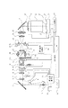
2 楕円集光ミラー
9 オプティカルインテグレータ
14 オプティカルインテグレータ
22 投影レンズ
23 マスク(原版)
25 ウェハ(感光基板)
32 可動ブラインド
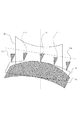
33 調整ブラインド(露光領域整形手段を調整する)
34 固定ブラインド
51 駆動点
60 開口エリア
66 遮光板
81 円形の有効部
82 矩形の露光領域
83 最大開口エリア
84 開口エリア
91 電源
92 露光量制御系
94 主制御系
95 ステージ制御系
96 露光範囲制御系
Claims (6)
- 光源からの光を用いて被照明面に配置されたマスクを照明する照明光学系を有し、前記マスクと基板とを相対的に移動させて、前記マスクのパターンを前記基板に投影する露光装置において、
前記照明光学系は、前記被照明面と共役な位置の近傍に配置された、開口幅が可変な開口可変機構を有し、
該開口可変機構が、一枚の遮光板と、該一枚の遮光板の複数箇所に対して力を加えるために、前記マスクと前記基板との相対移動の方向に対応する方向の駆動軸を有する複数の駆動機構とを含み、
該複数の駆動機構のうちの少なくとも1つの駆動機構が、1つの回動案内機構と、前記駆動軸に垂直な2軸方向に関する平面案内機構とを有することを特徴とする露光装置。 - 前記複数の駆動機構のうちの1つを除くすべての駆動機構が、前記回動案内機構と前記平面案内機構とを有することを特徴とする請求項1記載の露光装置。
- 前記2軸方向に関する平面案内機構は、互いに垂直な方向に案内する2つの案内機構を有することを特徴とする請求項1又は2記載の露光装置。
- 前記遮光板が、前記照明光学系の光軸に対して傾いていることを特徴とする請求項1乃至3いずれかに記載の露光装置。
- 前記開口可変機構の開口形状を矩形にも円弧にもすることが可能であることを特徴とする請求項1乃至4いずれかに記載の露光装置。
- 請求項1乃至5いずれかに記載の露光装置を用いて前記基板を露光する工程と、前記露光された基板を現像する工程とを有することを特徴とするデバイス製造方法。
Priority Applications (2)
| Application Number | Priority Date | Filing Date | Title |
|---|---|---|---|
| JP2003434549A JP4458329B2 (ja) | 2003-12-26 | 2003-12-26 | 露光装置及びデバイス製造方法 |
| US11/019,106 US7148948B2 (en) | 2003-12-26 | 2004-12-22 | Scanning exposure apparatus, and device manufacturing method |
Applications Claiming Priority (1)
| Application Number | Priority Date | Filing Date | Title |
|---|---|---|---|
| JP2003434549A JP4458329B2 (ja) | 2003-12-26 | 2003-12-26 | 露光装置及びデバイス製造方法 |
Publications (3)
| Publication Number | Publication Date |
|---|---|
| JP2005191495A JP2005191495A (ja) | 2005-07-14 |
| JP2005191495A5 JP2005191495A5 (ja) | 2007-02-08 |
| JP4458329B2 true JP4458329B2 (ja) | 2010-04-28 |
Family
ID=34791591
Family Applications (1)
| Application Number | Title | Priority Date | Filing Date |
|---|---|---|---|
| JP2003434549A Expired - Fee Related JP4458329B2 (ja) | 2003-12-26 | 2003-12-26 | 露光装置及びデバイス製造方法 |
Country Status (2)
| Country | Link |
|---|---|
| US (1) | US7148948B2 (ja) |
| JP (1) | JP4458329B2 (ja) |
Families Citing this family (11)
| Publication number | Priority date | Publication date | Assignee | Title |
|---|---|---|---|---|
| JP2007158225A (ja) * | 2005-12-08 | 2007-06-21 | Canon Inc | 露光装置 |
| JP2010123755A (ja) | 2008-11-19 | 2010-06-03 | Canon Inc | 露光装置及びデバイス製造方法 |
| US9494463B2 (en) * | 2009-05-07 | 2016-11-15 | Thermo Scientific Portable Analytical Instruments Inc. | Optical emission spectroscopic (OES) instrument with automatic top and bottom slit curtains |
| JP5127875B2 (ja) | 2010-04-28 | 2013-01-23 | キヤノン株式会社 | リソグラフィ装置及び物品の製造方法 |
| NL2007367A (en) | 2010-11-01 | 2012-05-02 | Asml Netherlands Bv | Lithographic apparatus and method. |
| JP6642969B2 (ja) * | 2015-02-16 | 2020-02-12 | キヤノン株式会社 | 光学ユニット、画像形成装置、および光学ユニットの製造方法 |
| JP6506599B2 (ja) * | 2015-04-15 | 2019-04-24 | キヤノン株式会社 | 照明光学系及び露光装置並びにデバイス製造方法 |
| JP6570298B2 (ja) * | 2015-04-15 | 2019-09-04 | キヤノン株式会社 | 照明光学系及び露光装置並びにデバイス製造方法 |
| JP6626273B2 (ja) * | 2015-06-03 | 2019-12-25 | キヤノン株式会社 | 露光装置及び物品の製造方法 |
| DE102016208174A1 (de) * | 2016-05-12 | 2017-04-27 | Carl Zeiss Smt Gmbh | Optisches system, insbesondere lithograpieanlage, sowie verfahren |
| JP7446069B2 (ja) * | 2019-09-03 | 2024-03-08 | キヤノン株式会社 | 露光装置及び物品の製造方法 |
Family Cites Families (10)
| Publication number | Priority date | Publication date | Assignee | Title |
|---|---|---|---|---|
| JPS60158449A (ja) | 1984-01-30 | 1985-08-19 | Canon Inc | 露光装置 |
| US4822975A (en) | 1984-01-30 | 1989-04-18 | Canon Kabushiki Kaisha | Method and apparatus for scanning exposure |
| JPS62193125A (ja) | 1986-02-19 | 1987-08-25 | Canon Inc | 露光むら補正装置 |
| JP3348928B2 (ja) | 1993-08-26 | 2002-11-20 | 株式会社ニコン | 走査露光方法、走査型露光装置、及び露光量制御装置 |
| US5777724A (en) | 1994-08-24 | 1998-07-07 | Suzuki; Kazuaki | Exposure amount control device |
| US6538723B2 (en) | 1996-08-05 | 2003-03-25 | Nikon Corporation | Scanning exposure in which an object and pulsed light are moved relatively, exposing a substrate by projecting a pattern on a mask onto the substrate with pulsed light from a light source, light sources therefor, and methods of manufacturing |
| JPH1050599A (ja) | 1996-08-05 | 1998-02-20 | Nikon Corp | 露光装置の制御方法 |
| US6013401A (en) * | 1997-03-31 | 2000-01-11 | Svg Lithography Systems, Inc. | Method of controlling illumination field to reduce line width variation |
| JP4392879B2 (ja) | 1998-09-28 | 2010-01-06 | キヤノン株式会社 | 投影露光装置及びデバイスの製造方法 |
| JP2001244183A (ja) | 2000-02-29 | 2001-09-07 | Canon Inc | 投影露光装置 |
-
2003
- 2003-12-26 JP JP2003434549A patent/JP4458329B2/ja not_active Expired - Fee Related
-
2004
- 2004-12-22 US US11/019,106 patent/US7148948B2/en not_active Expired - Lifetime
Also Published As
| Publication number | Publication date |
|---|---|
| JP2005191495A (ja) | 2005-07-14 |
| US20050162628A1 (en) | 2005-07-28 |
| US7148948B2 (en) | 2006-12-12 |
Similar Documents
| Publication | Publication Date | Title |
|---|---|---|
| TW546699B (en) | Exposure apparatus and exposure method capable of controlling illumination distribution | |
| JP2011040716A (ja) | 露光装置、露光方法、およびデバイス製造方法 | |
| JP3799275B2 (ja) | 走査露光装置及びその製造方法並びにデバイス製造方法 | |
| JP4458329B2 (ja) | 露光装置及びデバイス製造方法 | |
| US20040157143A1 (en) | Exposure method and lithography system, exposure apparatus and method of making the apparatus, and method of manufacturing device | |
| JP5387982B2 (ja) | 照明光学装置、露光装置、およびデバイス製造方法 | |
| TWI397788B (zh) | 致動系統、微影裝置及器件製造方法 | |
| JP2022106891A (ja) | 露光装置、フラットパネルディスプレイの製造方法、及びデバイス製造方法 | |
| JP4684563B2 (ja) | 露光装置及び方法 | |
| JP2001244183A (ja) | 投影露光装置 | |
| JP2006120798A (ja) | 露光装置 | |
| JP2007207821A (ja) | 可変スリット装置、照明装置、露光装置、露光方法及びデバイスの製造方法 | |
| JP2006245157A (ja) | 露光方法及び露光装置 | |
| JP2004226661A (ja) | 3次元構造形成方法 | |
| CN107783383B (zh) | 曝光装置、曝光方法以及物品制造方法 | |
| JP2010118403A (ja) | 走査型露光装置、及びデバイスの製造方法 | |
| JP4235410B2 (ja) | 露光方法 | |
| JP4838698B2 (ja) | 露光装置およびデバイス製造方法 | |
| JP4764161B2 (ja) | 露光装置、露光方法及びデバイス製造方法 | |
| JP2009164356A (ja) | 走査露光装置およびデバイス製造方法 | |
| JP4298305B2 (ja) | 露光装置及び半導体デバイスの製造方法 | |
| JP2005310942A (ja) | 露光装置、露光方法、及びそれを用いたデバイス製造方法 | |
| JP2001338866A (ja) | 露光装置、デバイスの製造方法および露光装置における精度測定方法 | |
| EP0831376A2 (en) | Scanning exposure method and mask therefor | |
| JPH07301845A (ja) | 絞り装置及びそれを用いた投影露光装置 |
Legal Events
| Date | Code | Title | Description |
|---|---|---|---|
| A521 | Request for written amendment filed |
Free format text: JAPANESE INTERMEDIATE CODE: A523 Effective date: 20061218 |
|
| A621 | Written request for application examination |
Free format text: JAPANESE INTERMEDIATE CODE: A621 Effective date: 20061218 |
|
| A977 | Report on retrieval |
Free format text: JAPANESE INTERMEDIATE CODE: A971007 Effective date: 20090916 |
|
| A131 | Notification of reasons for refusal |
Free format text: JAPANESE INTERMEDIATE CODE: A131 Effective date: 20090924 |
|
| A521 | Request for written amendment filed |
Free format text: JAPANESE INTERMEDIATE CODE: A523 Effective date: 20091124 |
|
| TRDD | Decision of grant or rejection written | ||
| A01 | Written decision to grant a patent or to grant a registration (utility model) |
Free format text: JAPANESE INTERMEDIATE CODE: A01 Effective date: 20100126 |
|
| A01 | Written decision to grant a patent or to grant a registration (utility model) |
Free format text: JAPANESE INTERMEDIATE CODE: A01 |
|
| RD04 | Notification of resignation of power of attorney |
Free format text: JAPANESE INTERMEDIATE CODE: A7424 Effective date: 20100201 |
|
| A61 | First payment of annual fees (during grant procedure) |
Free format text: JAPANESE INTERMEDIATE CODE: A61 Effective date: 20100203 |
|
| R150 | Certificate of patent or registration of utility model |
Free format text: JAPANESE INTERMEDIATE CODE: R150 Ref document number: 4458329 Country of ref document: JP Free format text: JAPANESE INTERMEDIATE CODE: R150 |
|
| FPAY | Renewal fee payment (event date is renewal date of database) |
Free format text: PAYMENT UNTIL: 20130219 Year of fee payment: 3 |
|
| FPAY | Renewal fee payment (event date is renewal date of database) |
Free format text: PAYMENT UNTIL: 20140219 Year of fee payment: 4 |
|
| LAPS | Cancellation because of no payment of annual fees |