JP4458329B2 - Exposure apparatus and device manufacturing method - Google Patents
Exposure apparatus and device manufacturing method Download PDFInfo
- Publication number
- JP4458329B2 JP4458329B2 JP2003434549A JP2003434549A JP4458329B2 JP 4458329 B2 JP4458329 B2 JP 4458329B2 JP 2003434549 A JP2003434549 A JP 2003434549A JP 2003434549 A JP2003434549 A JP 2003434549A JP 4458329 B2 JP4458329 B2 JP 4458329B2
- Authority
- JP
- Japan
- Prior art keywords
- exposure
- slit
- wafer
- exposure apparatus
- guide mechanism
- Prior art date
- Legal status (The legal status is an assumption and is not a legal conclusion. Google has not performed a legal analysis and makes no representation as to the accuracy of the status listed.)
- Expired - Fee Related
Links
- 238000004519 manufacturing process Methods 0.000 title claims description 16
- 230000007246 mechanism Effects 0.000 claims description 101
- 230000003287 optical effect Effects 0.000 claims description 64
- 238000005286 illumination Methods 0.000 claims description 40
- 239000000758 substrate Substances 0.000 claims description 21
- 235000012431 wafers Nutrition 0.000 description 83
- 238000000034 method Methods 0.000 description 26
- 239000002184 metal Substances 0.000 description 21
- 238000009826 distribution Methods 0.000 description 19
- 230000008569 process Effects 0.000 description 9
- 230000008859 change Effects 0.000 description 8
- 239000004065 semiconductor Substances 0.000 description 8
- 238000007493 shaping process Methods 0.000 description 8
- 238000012546 transfer Methods 0.000 description 8
- 230000035945 sensitivity Effects 0.000 description 5
- 230000007423 decrease Effects 0.000 description 4
- 238000003384 imaging method Methods 0.000 description 4
- 239000004973 liquid crystal related substance Substances 0.000 description 4
- 238000005259 measurement Methods 0.000 description 4
- 239000003795 chemical substances by application Substances 0.000 description 3
- 239000000463 material Substances 0.000 description 3
- 239000010409 thin film Substances 0.000 description 3
- XUIMIQQOPSSXEZ-UHFFFAOYSA-N Silicon Chemical compound [Si] XUIMIQQOPSSXEZ-UHFFFAOYSA-N 0.000 description 2
- 230000002159 abnormal effect Effects 0.000 description 2
- 230000004075 alteration Effects 0.000 description 2
- 239000011248 coating agent Substances 0.000 description 2
- 238000000576 coating method Methods 0.000 description 2
- 238000012790 confirmation Methods 0.000 description 2
- 238000012937 correction Methods 0.000 description 2
- 238000006073 displacement reaction Methods 0.000 description 2
- 238000005530 etching Methods 0.000 description 2
- 239000011521 glass Substances 0.000 description 2
- 238000007689 inspection Methods 0.000 description 2
- 230000010354 integration Effects 0.000 description 2
- 238000001459 lithography Methods 0.000 description 2
- 229910052710 silicon Inorganic materials 0.000 description 2
- 239000010703 silicon Substances 0.000 description 2
- 238000012360 testing method Methods 0.000 description 2
- 238000002834 transmittance Methods 0.000 description 2
- 238000005452 bending Methods 0.000 description 1
- 230000015572 biosynthetic process Effects 0.000 description 1
- 238000003486 chemical etching Methods 0.000 description 1
- 238000005520 cutting process Methods 0.000 description 1
- 238000013461 design Methods 0.000 description 1
- 238000011161 development Methods 0.000 description 1
- 238000005538 encapsulation Methods 0.000 description 1
- 238000005516 engineering process Methods 0.000 description 1
- 230000007613 environmental effect Effects 0.000 description 1
- 230000001747 exhibiting effect Effects 0.000 description 1
- 239000010408 film Substances 0.000 description 1
- 238000005468 ion implantation Methods 0.000 description 1
- 150000002500 ions Chemical class 0.000 description 1
- 230000003647 oxidation Effects 0.000 description 1
- 238000007254 oxidation reaction Methods 0.000 description 1
- 238000012858 packaging process Methods 0.000 description 1
- 238000000206 photolithography Methods 0.000 description 1
- 229920002120 photoresistant polymer Polymers 0.000 description 1
- 230000009467 reduction Effects 0.000 description 1
- 230000001235 sensitizing effect Effects 0.000 description 1
- 230000001360 synchronised effect Effects 0.000 description 1
- 230000002123 temporal effect Effects 0.000 description 1
- 238000007740 vapor deposition Methods 0.000 description 1
Images


Classifications
-
- G—PHYSICS
- G03—PHOTOGRAPHY; CINEMATOGRAPHY; ANALOGOUS TECHNIQUES USING WAVES OTHER THAN OPTICAL WAVES; ELECTROGRAPHY; HOLOGRAPHY
- G03F—PHOTOMECHANICAL PRODUCTION OF TEXTURED OR PATTERNED SURFACES, e.g. FOR PRINTING, FOR PROCESSING OF SEMICONDUCTOR DEVICES; MATERIALS THEREFOR; ORIGINALS THEREFOR; APPARATUS SPECIALLY ADAPTED THEREFOR
- G03F7/00—Photomechanical, e.g. photolithographic, production of textured or patterned surfaces, e.g. printing surfaces; Materials therefor, e.g. comprising photoresists; Apparatus specially adapted therefor
- G03F7/70—Microphotolithographic exposure; Apparatus therefor
- G03F7/70058—Mask illumination systems
- G03F7/70083—Non-homogeneous intensity distribution in the mask plane
-
- G—PHYSICS
- G03—PHOTOGRAPHY; CINEMATOGRAPHY; ANALOGOUS TECHNIQUES USING WAVES OTHER THAN OPTICAL WAVES; ELECTROGRAPHY; HOLOGRAPHY
- G03F—PHOTOMECHANICAL PRODUCTION OF TEXTURED OR PATTERNED SURFACES, e.g. FOR PRINTING, FOR PROCESSING OF SEMICONDUCTOR DEVICES; MATERIALS THEREFOR; ORIGINALS THEREFOR; APPARATUS SPECIALLY ADAPTED THEREFOR
- G03F7/00—Photomechanical, e.g. photolithographic, production of textured or patterned surfaces, e.g. printing surfaces; Materials therefor, e.g. comprising photoresists; Apparatus specially adapted therefor
- G03F7/70—Microphotolithographic exposure; Apparatus therefor
- G03F7/70058—Mask illumination systems
- G03F7/70066—Size and form of the illuminated area in the mask plane, e.g. reticle masking blades or blinds
-
- G—PHYSICS
- G03—PHOTOGRAPHY; CINEMATOGRAPHY; ANALOGOUS TECHNIQUES USING WAVES OTHER THAN OPTICAL WAVES; ELECTROGRAPHY; HOLOGRAPHY
- G03F—PHOTOMECHANICAL PRODUCTION OF TEXTURED OR PATTERNED SURFACES, e.g. FOR PRINTING, FOR PROCESSING OF SEMICONDUCTOR DEVICES; MATERIALS THEREFOR; ORIGINALS THEREFOR; APPARATUS SPECIALLY ADAPTED THEREFOR
- G03F7/00—Photomechanical, e.g. photolithographic, production of textured or patterned surfaces, e.g. printing surfaces; Materials therefor, e.g. comprising photoresists; Apparatus specially adapted therefor
- G03F7/70—Microphotolithographic exposure; Apparatus therefor
- G03F7/70483—Information management; Active and passive control; Testing; Wafer monitoring, e.g. pattern monitoring
- G03F7/7055—Exposure light control in all parts of the microlithographic apparatus, e.g. pulse length control or light interruption
- G03F7/70558—Dose control, i.e. achievement of a desired dose
Description
本発明は、照明光の制御可能な露光装置に係り、更に詳しくは、ICやLSI等の半導体素子、液晶表示素子または薄膜磁気ヘッド等をフォトリソグラフィ工程で製造する際に使用される所謂スリットスキャン露光方式またはステップ・アンド・スキャン方式などの照明光の制御可能な走査型投影露光装置に関するものである。 The present invention relates to an exposure apparatus capable of controlling illumination light, and more specifically, a so-called slit scan used when manufacturing a semiconductor element such as an IC or LSI, a liquid crystal display element or a thin film magnetic head in a photolithography process. The present invention relates to a scanning projection exposure apparatus capable of controlling illumination light such as an exposure method or a step-and-scan method.
半導体素子や液晶表示素子および薄膜磁気ヘッドを製造する際に、リソグラフィ技術を利用して、マスクないしはレチクルと呼ばれる原版(以下、代表してマスクと呼ぶ)の表面に形成されたパターンを、レジストと呼ばれる感光材をシリコンウエハやガラス基板の表面に塗布した感光基板(以下、代表してウエハと呼ぶ)上に転写する為に、レジストを感光させるための照明光を、前記原版を通して感光基板上に露光する、投影露光装置が使用されている。 When manufacturing semiconductor elements, liquid crystal display elements, and thin-film magnetic heads, a pattern formed on the surface of an original plate called a mask or reticle (hereinafter referred to as a mask) using a lithography technique is used as a resist. In order to transfer a photosensitive material called a photosensitive material applied to the surface of a silicon wafer or a glass substrate (hereinafter referred to as a wafer), illumination light for sensitizing the resist is applied to the photosensitive substrate through the original plate. A projection exposure apparatus that performs exposure is used.
従来、投影露光装置には原版と感光基板を密着ないしは近接させて一括露光を行うプロキシミティ露光方式や、ミラー反射光学系を介して円孤状の露光光を原版と感光基板上で走査露光するミラープロジェクション露光方式や、感光基板上の各露光領域を投影光学系の露光領域に順次移動させながら原版の縮小露光像を一括露光するというステップ・アンド・リピート方式の縮小投影型露光装置(所謂、ステッパ)が使用されていた。 Conventionally, in a projection exposure apparatus, a proximity exposure method in which the original and the photosensitive substrate are brought into close contact or close to each other and a batch exposure is performed, or circular exposure light is scanned and exposed on the original and the photosensitive substrate through a mirror reflection optical system. A mirror projection exposure method or a step-and-repeat reduction projection exposure apparatus (so-called so-called so-called “step-and-repeat” method) that collectively exposes a reduced exposure image of an original while moving each exposure area on a photosensitive substrate to an exposure area of a projection optical system. Stepper) was used.
一括露光方式であるステップ・アンド・リピート方式の露光装置では、投影光学系がレンズによって構成されている場合、有効な結像領域は円形状となるが、半導体集積回路は一般的に矩形であるため、使用される原版も当然のごとく矩形形状をなしており、一括露光の場合の転写領域を最大限に確保しようとすれば、投影光学系の有する円形の結像領域に内接する矩形の領域となり、最も大きな転写領域でも円の直径の1/√2の辺の正方形である。 In a step-and-repeat exposure apparatus that is a batch exposure method, when the projection optical system is constituted by a lens, an effective imaging region is circular, but a semiconductor integrated circuit is generally rectangular. Therefore, the original plate to be used has a rectangular shape as a matter of course, and if it is intended to secure the maximum transfer area in the case of batch exposure, a rectangular area inscribed in the circular imaging area of the projection optical system. Thus, even the largest transfer region is a square with sides of 1 / √2 of the diameter of the circle.
これに対して、投影光学系の有する円形状の結像領域のほぼ直径の寸法を有する矩形形状の露光領域を用いて、マスクとウエハとを同期させながら走査移動させることによって、転写領域を拡大させる走査露光方式である所謂スリットスキャン露光方式またはステップ・アンド・スキャン方式(以下、代表してスリットスキャン方式と呼ぶ)が提案されている。 On the other hand, the transfer area is enlarged by scanning and moving the mask and the wafer in synchronization with each other using a rectangular exposure area having a diameter almost equal to that of the circular imaging area of the projection optical system. A so-called slit scan exposure method or a step-and-scan method (hereinafter referred to as a slit scan method) has been proposed.
スリットスキャン方式の投影露光装置については、例えばOplusEの1993年2月号の96〜99頁に詳しく紹介されているが、該露光装置は矩形の露光領域を有し、各ショットに対し該スリットをスキャン(走査)して走査露光が行われ、1つのショットの走査露光が終了するとウエハは次のショットにステップし、次のショットの走査露光が同様に繰り返され、次のショットヘのステップと露光のためのスキャンとを繰り返すことによって、ウエハ全体の露光が完了するという露光工程を有している。 The slit scanning type projection exposure apparatus is described in detail in, for example, pages 96 to 99 of the February 1993 issue of Oplus E. The exposure apparatus has a rectangular exposure area, and the slit is provided for each shot. The scanning exposure is performed by scanning, and when the scanning exposure of one shot is completed, the wafer steps to the next shot, and the scanning exposure of the next shot is repeated in the same manner. The exposure process of completing the exposure of the entire wafer is performed by repeating the scan for this.
このようなスリットスキャン方式では、同一の大きさの結像領域を有する投影光学系を用いた場合、投影レンズを用いて各転写領域ごとに一括露光を行うステップ・アンド・リピート方式に比べてより大きな転写領域を確保することができる。すなわち、走査方向に対しては光学系による制限がなくなるので走査ステージのストローク分だけ確保することができ、走査方向に対して直角な方向には概ね√2倍の転写領域を確保することができる。 In such a slit scan method, when a projection optical system having an imaging region of the same size is used, compared to a step-and-repeat method in which batch exposure is performed for each transfer region using a projection lens. A large transfer area can be secured. In other words, since there is no restriction by the optical system in the scanning direction, it is possible to ensure only the stroke of the scanning stage, and it is possible to ensure a transfer area approximately √2 times in the direction perpendicular to the scanning direction. .
半導体集積回路を製造するための露光装置は、高い集積度のチップの製造に対応するために、転写領域の拡大と解像力の向上が望まれており、より小さい投影光学系を採用できることは、光学性能上からも、コスト的にも有利であり、スリットスキャン方式の露光方法は、今後の露光装置の主流として注目されている。 An exposure apparatus for manufacturing a semiconductor integrated circuit is required to expand a transfer area and improve resolution in order to cope with manufacture of a highly integrated chip. From the viewpoint of performance, it is advantageous in terms of cost, and the exposure method of the slit scan method is attracting attention as a mainstream of future exposure apparatuses.
図10は特開平10−50599号公報に開示されたスリットスキャン方式の投影露光装置の構成を示すものであるが、同図において光源1より発せられた照明光は楕円集光ミラー2によって集光された後に、オプティカル・インテグレータ9、14(14a、14b)によって像面照度の重畳化(平均化)が行われ、第1のリレーレンズ42を経た後に、2枚の可動ブレードを有する可動ブラインド(可動視野絞り)32に至る。可動ブラインド32はオプティカル・インテグレータ14のフーリエ変換面となっており、マスク23と光学的に共役な位置に配置されていて、さらに、その近傍には固定ブラインド(視野絞り)34が配置されている。固定ブラインド34は例えば4個のナイフエッジにより矩形の開口を囲んだ機械的な視野絞りであって、その矩形の開口形状によってマスク23上の照明領域の形状が規定されている。即ち、可動ブラインド32、及び固定ブラインド34により制限された照明光が第2リレーレンズ35、コンデンサレンズ36、及びミラー11を介してマスク23上の照明領域を均一な照度分布で照明している。以上の照明条件の下で、アライメントマーク28を用いてマスク23とウエハ25との位置合わせを行った上で、マスク23とウエハ25をウエハ25の面内の第1の方向(以下スキャン方向と呼ぶ)に同期スキャンすることによりウエハ25上に塗布したフォトレジストが感光し、マスク23に形成されているパターンがウエハ25上に精密に転写される。
FIG. 10 shows the configuration of a slit scanning projection exposure apparatus disclosed in Japanese Patent Laid-Open No. 10-50599. In FIG. 10, illumination light emitted from a light source 1 is condensed by an elliptical condensing mirror 2. After that, the optical integrators 9 and 14 (14a and 14b) superimpose (average) the image surface illuminance, and after passing through the
スリットスキャン方式の投影露光装置ではウエハ25上の各露光領域をこれらの露光領域のスキャン方向の長さより短い矩形の開口による走査露光によって露光が行われるので、各露光領域内の積算露光量の制御は、その矩形開口部の積算露光量をウエハ25上の全ての点で一定となる様に実行する必要がある。仮に、ウエハ25上の各点での積算露光量が異なると、各露光領域内での積算露光量にムラが生じることとなり、これはステップ・アンド・リピート方式の露光装置における照度ムラと同様の誤差となってしまう。前記、照度ムラに対する解決手段としてスリットスキャン方式の露光装置で、特に等速露光装置においては、例えば特開昭60−158449号公報や特開平7−66103号公報に示されるように、ウエハ25上の露光量の均一化を図るために、スキャン方向の照度分布を台形にすることが行われている。従ってウエハ25上の矩形状の露光領域内の任意の一点で露光中の照度の時間的変化は図6(A)に示されるように台形状となり、この事は、等速走査露光においてはそのまま時間軸を空間軸に変換して考えることができるので、空間軸上でも図6(B)に示すような照度分布を示すこととなる。
In the projection exposure apparatus of the slit scan system, each exposure area on the
等速走査露光における露光量制御は、この台形状の照度分布を高さと面積が等しい矩形と見做し、図6(B)における幅L×高さIの矩形をはみ出した三角形部分と、矩形内の三角形部分との面積が等しくなる点、即ち、両側の斜線部において最高照度Iの1/2となる点を結んだ線の幅Lを有し、高さが等しい矩形に近似している。そして、この矩形の幅Lをスリットの幅としている。 In the exposure amount control in the constant speed scanning exposure, the trapezoidal illuminance distribution is regarded as a rectangle having the same height and area, and a triangle portion protruding from the rectangle of width L × height I in FIG. It has a width L of a line connecting points that have the same area as the inner triangular part, that is, a point that is ½ of the maximum illuminance I in the hatched part on both sides, and approximates a rectangle having the same height. . The width L of the rectangle is the width of the slit.
これらの従来例はスキャン方向に関する照度ムラの補正までを考慮したものであって、固定ブラインド34の開口形状はあくまで、矩形としており、スキャン方向の開口幅が一定の値となっている。固定ブラインド34の開口形状が矩形であることは、マスク23上およびウエハ25上に投影される開口形状も当然のことながら矩形となっており、マスク23上およびウエハ25上で、スキャン方向と直交する方向(以下、スリット方向と呼ぶ)にも照度が均一でなければ、露光ムラが発生してしまう。
These conventional examples consider the correction of illuminance unevenness in the scanning direction, and the opening shape of the fixed blind 34 is a rectangular shape, and the opening width in the scanning direction is a constant value. Since the opening shape of the fixed blind 34 is rectangular, the opening shape projected onto the
前記したように、可動ブラインド32はマスク23と光学的に共役な位置に配されており、更に固定ブラインド34は可動ブラインド32の近傍に配置されているが、固定ブラインド34の位置において照明範囲内が必ずしも均一な照度分布となっているとは限らない。即ち、光源1から固定ブラインド34に至るまでの光路中に配された光学素子の製造上の誤差や、組立時の誤差による光路長の変位等により、固定ブラインド34の位置で光軸と直交する面内には若干の照度ムラが発生しているのが一般的である。
As described above, the movable blind 32 is disposed at a position optically conjugate with the
従って、固定ブラインド34によって、照明領域を矩形に制限してマスク23上を照明し、更に、投影レンズ22を通してウエハ25を照明した場合に、露光位置によって積算露光量にバラツキが発生し、均一な露光ができずウエハ25上に塗布されたレジストは場所によって感光状態に差異が生じることとなる。仮に、固定ブラインド34の位置での照度ムラが全く無いように、光学系の調整を行ったと仮定しても、マスク23上の像をウエハ25上に結像するための投影レンズ22は10枚から数十個の光学素子によって構成されており、それぞれの光学素子の製造誤差や光学素子上に施されたコーティングのムラ等によって、照明光の透過率に部分的なムラが発生している。
Therefore, when the illumination area is limited to a rectangular shape by the fixed blind 34 and the
図2(A)はマスク23上でスリット方向に関する照明光の照度i(x)の分布を示すものであるが、図に示されるように照度分布が均一であったとしても、前記、投影レンズ22の透過率のムラによって、ウエハ25上の照度I(x)の分布は図2(B)に示すように、不均一な分布となってしまう。
FIG. 2A shows the distribution of the illuminance i (x) of the illumination light in the slit direction on the
ここで、投影レンズ22で発生する透過率のムラについて、さらに説明する。図8(A)は投影レンズ22のウエハ25上の有効領域を示すものであるが、投影レンズ22は一般的に外周が円形の光学素子の組み合わせによって成り立っているために、レンズ自体では円形の有効部81を有しているが、前述したように、スリットスキャン方式の露光装置では広い幅でスキャン露光を行うためにレンズの有効部81の中で、矩形の露光領域82を使用している。この時、前記、光学素子上の製造誤差や光学素子上に施されたコーティングのムラ、あるいは組立の誤差に起因する照度ムラは、一般に光学素子の径方向に相関を持つ分布で発生するため、矩形の露光領域内の照度分布は、図9に示すように紡錘形を切り出したような形状となってしまい、このような照度分布を持った露光光を用いて、マスク23とウエハ25とを同期走査した場合、スリット方向に関する積算露光量は、場所毎に大きな照度ムラを有する結果を招く。
Here, the non-uniformity in transmittance generated in the
以上の不具合を改善する手段として、例えば特開昭62−193125号公報に開示されている投影露光装置では、照明光の光路中に液晶シャッタを挿入し、露光光の照射エリアを自由にできるように構成されており、露光光の強度が低く積算露光量の不足する位置ではスキャン方向の開口幅を拡大し、逆に、露光光の強度が高くて積算露光量が大きすぎる位置ではスキャン方向の開口幅を狭くするような制御を加えているが、このような従来例においては、開口幅を変更する機能・手段について説明がなされているものの、投影露光が効率的に行われるように開口幅を決定する方法には言及していない。 As a means for improving the above problems, for example, in a projection exposure apparatus disclosed in Japanese Patent Laid-Open No. 62-193125, a liquid crystal shutter is inserted in the optical path of illumination light so that the exposure light irradiation area can be freely set. The aperture width in the scan direction is enlarged at a position where the exposure light intensity is low and the accumulated exposure amount is insufficient, and conversely, at the position where the exposure light intensity is too high and the accumulated exposure amount is too large, Although control to reduce the aperture width is added, in such a conventional example, functions and means for changing the aperture width are described, but the aperture width is set so that the projection exposure is performed efficiently. It does not mention how to determine.
例えば、ウエハ25上に塗布された感光剤であるレジストの感光感度をPrとし、ウエハ25面上に露光される単位時間当たりの露光量をQw、ウエハ25上に投影される固定ブラインド34のスキャン方向の開口幅をLw、ウエハ25のスキャン方向への移動速度をVwとすると、ウエハ25上での積算露光量はレジストの感光感度に等しいため、
Pr=Qw×Lw÷Vw・・・(式1)
と表現されるので、
Vw=Qw×Lw÷Pr・・・(式2)
と書き換えられ、レジストの感度Prを2,000J/m2、ウエハ25面上に露光される単位当たりの露光量(以下ウエハ面照度と呼ぶ)Qwを30,000W/m2、スキャン方向の開口幅Lwを10mmとすると、ウエハ25のスキャン速度Vwは0.15m/secとなる。しかし、ここで光源1の出力が低下してウエハ面照度Qwが20,000W/m2まで低下すると、スキャン速度Vwは0.10m/secに低下する。このことは露光に要する時間が長くなることを意味し、生産性の低下を招く結果となる。
For example, the photosensitive sensitivity of a resist that is a photosensitive agent applied on the
Pr = Qw × Lw ÷ Vw (Formula 1)
It is expressed as
Vw = Qw × Lw ÷ Pr (Formula 2)
And the resist sensitivity Pr is 2,000 J / m 2 , the exposure amount per unit exposed on the surface of the wafer 25 (hereinafter referred to as wafer surface illuminance) Qw is 30,000 W / m 2 , and the opening in the scanning direction When the width Lw is 10 mm, the scanning speed Vw of the
ここで、(式2)により、スキャン方向の開口幅Lwを広げることによってスキャン速度の向上を図ることができるが、その反面投影レンズ22には光学性能を十分に発揮するための有効画角が決まっており、むやみに開口幅を広げることができない。従って、前記従来例において、照度ムラにあわせてスキャン方向の開口幅を局所的に調整を行う際にも、スキャン方向の最大開口幅に着目して、効率的な露光を行うための開口幅の決定方法が必要となってくる。
Here, according to (Equation 2), the scanning speed can be improved by widening the opening width Lw in the scanning direction. However, the
特開2001−244183号広報は上述の従来技術に付随する不都合点に鑑みてなされたものであって、該出願に係る第1及び第2の発明は、投影レンズ22の画角を有効に利用しながら、ウエハ25上に発生する照度ムラの量を低減し無くすために局所的に調整可能とすることを目的としており、該出願に係る第3及び第4の発明は、露光装置上で使用される複数の露光条件のすべてに対して、前記照度ムラを減らし無くすための調整を可能とすることを目的としている。
Japanese Laid-Open Patent Publication No. 2001-244183 is made in view of the disadvantages associated with the above-described conventional technology, and the first and second inventions according to the application effectively use the angle of view of the
特開2001−244183号広報は図1及び図5に示すように、照明光の光軸に対して傾斜して取り付けられた可撓性のある遮光板66(66a,66b)によってウエハ25上に照射される露光量の部分的なムラを無くすための調整機構を構成している。遮光板66は前記光軸に対して相対した位置に一対66a,66bとなって取り付けられているものであり、プッシュロッド51a、51b、51c、51d、51eの押し引きによって変形可能となっていて、遮光板66を任意の形状に変形させることによって、照明光の開口エリア60の形状が決定されるように構成されている。
As shown in FIGS. 1 and 5, Japanese Patent Laid-Open No. 2001-244183 discloses that a flexible light-shielding plate 66 (66 a, 66 b) mounted on the
調整ブラインド33について、図5を用いて更に詳しく説明すると、遮光板66は厚さ0.1mmの金属板であってその表面はケミカルエッチングによって梨地状の拡散面となっており、図5に示すように遮光板66は照明光の光軸に対して約40度の傾きを持って配置されている。この角度は、特開2001−244183号広報の実施例では第3リレーレンズ42にN.A.=0.35程度のものを使用しており、照明光は光軸に対して約19度の広がり角を持っている為であって、照明光が可動ブラインド32の面上に集光する直前で遮光板66を挿入して開口幅を狭める際に、遮光板66の光軸側のエッジによって開口幅を決定できるように、第3リレーレンズ42の広がり角よりも急角度に設定されている。
The adjustment blind 33 will be described in more detail with reference to FIG. 5. The
また、図1では遮光板66の変形状態を表している。本実施例ではウエハ25上での標準的な照度ムラに合わせて、予め調整ブラインド33の開口形状が矩形とは若干異なる形状に設定されている。開口形状の詳細については後述するが、本実施例での開口形状60は図1に示すように鼓型をしており、遮光板66はこの開口形状60に合わせて、プッシュロッド51a、51b、51c、51d、51eが押し引きされている。しかし、遮光板66の光軸側のエッジが直線であった場合、プッシュロッド51a、51b、51c、51d、51eの押し引きによってこのように遮光板66を変形させると、遮光板66は光軸に対して傾けて配置されているため、変形を受けた部分は、調整ブラインド33の面内だけではなく、光軸方向にも変形を受けてしまい、マスク23と共役な位置にある可動ブラインド32に対するデフォーカス量が変化してしまう。
Further, FIG. 1 shows a deformed state of the
このようにデフォーカス量が変化しても、ウエハ25上の照度分布を考えると、図6(A)に示す台形の斜辺部分の角度が変化するだけで、台形の面積は変化しないので、積算照度の変化は見られないが、遮光板66が光軸方向にも変形を起こしてしまう分だけ、図5における可動ブラインド32と調整ブラインド33の遮光板66a,66bとの間隔△dを広げておく必要が生じてしまう。
Even if the defocus amount changes in this way, considering the illuminance distribution on the
このような事態を回避するため、特開2001−244183号広報の実施例に係る遮光板66は図1に示すように、あらかじめ楕円状のエッジ形状をしており、前記の鼓型開口形状60に変形させた時点で、遮光板66のエッジが光軸に対して垂直な面内に収まるようになっている。
In order to avoid such a situation, as shown in FIG. 1, the
もちろん、調整ブラインド33の開口形状60は標準状態でのみ使用されるものではないが、ウエハ25上に発生する照度ムラの変化量は、後述する照明条件の変更や、光学素子の経時的変化によって1〜3パーセント程度であるので、遮光板66の変形量も小さくて済むようになっている。
Of course, the opening
特開2001−244183号広報に係る第1の発明は、原版と感光基板を同期させて第1の方向へ走査して、前記原版上のパターンを前記感光基板上に露光する投影露光装置において、照明光学系内の前記原版と共役な位置の近傍に、前記第1の方向に関する露光領域の開口幅を、前記第1の方向と直交する第2の方向に関して局所的に変更する露光領域整形手段を具備し、前記露光領域整形手段によって、前記露光領域を任意の形状に整形して、前記感光基板上に照射される露光光量の部分的なムラを無くすための調整機能を有しており、前記露光領域整形手段の前記第1の方向に関する最大開口幅は、投影レンズの前記第1の方向に関する最大画角に相当することを特徴とする。 In a projection exposure apparatus that scans in a first direction in synchronization with an original plate and a photosensitive substrate and exposes a pattern on the original plate on the photosensitive substrate, An exposure area shaping means for locally changing the opening width of the exposure area in the first direction in the vicinity of the position conjugate with the original plate in the illumination optical system in the second direction orthogonal to the first direction. And having an adjustment function for shaping the exposure area into an arbitrary shape by the exposure area shaping means to eliminate partial unevenness in the amount of exposure light irradiated on the photosensitive substrate, The maximum aperture width in the first direction of the exposure area shaping means corresponds to the maximum field angle in the first direction of the projection lens.
これによれば、照明光を生成するための照明光学系及び投影レンズによって発生する局所的な照度ムラに適応して開口幅を調整し、均一な露光分布を形成するとともに、開口幅の調整の際に最大開口幅を投影レンズの最大画角に相当することによって、投影レンズに関する最大の露光光量を得ることができる。 According to this, the aperture width is adjusted to adapt to local illuminance unevenness generated by the illumination optical system for generating the illumination light and the projection lens, and a uniform exposure distribution is formed, and the aperture width is adjusted. When the maximum aperture width corresponds to the maximum angle of view of the projection lens, the maximum amount of exposure light for the projection lens can be obtained.
従って、原版と感光基板とを同期走査してスキャン露光を行う際の、スキャン速度は前記投影レンズに関する最大の速度を使用することが可能であり、露光装置の生産性が向上するものである。 Accordingly, when performing scanning exposure by synchronously scanning the original and the photosensitive substrate, the maximum scanning speed for the projection lens can be used, and the productivity of the exposure apparatus is improved.
また、特開2001−244183号広報に係る第2の発明は、前記第1の発明において、感光基板と同一な面内で、スリット方向に関して、位置毎に照明光量を測定し、測定された照明光量が概ね一様となりムラが無くなる様に、前記露光領域整形手段を駆動する機能を有することを特徴としており、露光の際に感光剤であるレジストが存在するべき位置での照度ムラを測定することが可能となるため、測定位置以降で照度ムラの発生する要因を完全に排除することが可能となっている。 In addition, in a second invention related to public information in Japanese Patent Application Laid-Open No. 2001-244183, in the first invention, the illumination light amount is measured at each position in the same plane as the photosensitive substrate with respect to the slit direction. It has a function of driving the exposure area shaping means so that the amount of light is substantially uniform and the unevenness is eliminated, and it measures illuminance unevenness at a position where a resist as a photosensitive agent should be present during exposure. Therefore, it is possible to completely eliminate the factor that causes illuminance unevenness after the measurement position.
また、特開2001−244183号広報に係る第3の発明は前記第1の発明において、前記原版に対する照明条件変更がされるたびに、露光光量の部分的な調整を行うことを特徴としており、原版に対する照明条件の変更によって、光路中の光学素子が変更されたり、あるいは、光路中の光学素子の使用部分が変わることによって生じる照度ムラの変化があった場合であっても、照度ムラの補正を新たにやり直すことができるので、常に均一な露光分布を得ることが可能となっている。 In addition, the third invention according to the publication of Japanese Patent Application Laid-Open No. 2001-244183 is characterized in that, in the first invention, the exposure light quantity is partially adjusted every time the illumination condition for the original is changed, Even if there is a change in illuminance unevenness caused by changes in the optical elements in the optical path due to changes in the illumination conditions for the original plate, or changes in the use part of the optical elements in the optical path, correction of illuminance unevenness Therefore, it is possible to always obtain a uniform exposure distribution.
さらに、特開2001−244183号広報に係る第4の発明は前記第3の発明において、前記照明条件の変更工程に、前記感光基板の露光面における照度分布を計測する段階を含むことを特徴としており、照明条件の変更と照度ムラの確認の作業が一連の動作として連続的に行われるため、作業者のミスによる測定忘れ等を防止することが可能となっている。
しかしながら、これらの従来例はスリットのスキャン方向の開口幅を局所的に変えることについて言及しているだけであり、それを実現するための具体的な機構については示していない。また、前記照度ムラの変化量1〜3パーセントを薄肉金属板で形成されたスリットの撓みで補正する場合、単純にスキャン方向に押し引きすると、機構に無理な応力が働いてアクチュエータの負荷が極めて大きくなり、薄肉金属板が塑性変形する危険性も生じる。したがって、薄肉金属板で形成された可変スリットを板の厚さ方向に無理なく変形させる手段が必要である。さらには、投影光学系にエネルギー効率、色収差、対環境敏感度の点から光学系内に複数のミラーとレンズを配置したカタディオプトリックタイプを選択し、スリットの開口形状が円弧状であるスキャニング式投影露光装置に適用させる必要も生じている。 However, these conventional examples only refer to locally changing the opening width of the slit in the scanning direction, and do not show a specific mechanism for realizing it. In addition, when correcting the variation of the illuminance unevenness by 1 to 3% by the bending of the slit formed of a thin metal plate, if the actuator is simply pushed and pulled in the scanning direction, an excessive stress is applied to the mechanism and the load on the actuator is extremely high. There is also a risk that the thin metal plate is plastically deformed. Therefore, there is a need for a means for easily deforming the variable slit formed of a thin metal plate in the thickness direction of the plate. In addition, the catadioptric type in which multiple mirrors and lenses are arranged in the optical system is selected for the projection optical system in terms of energy efficiency, chromatic aberration, and environmental sensitivity, and the scanning type has an arc shape in the slit opening. There is also a need for application to a projection exposure apparatus.
ところが、前記スリットのエッジ近傍のマスク共役面には、マスクの照射領域を制限するブラインド機構が配置されており、露光ムラ調整スリット機構と該ブラインド機構との干渉が問題となる。 However, a blind mechanism for limiting the irradiation area of the mask is disposed on the mask conjugate surface in the vicinity of the edge of the slit, and interference between the exposure unevenness adjusting slit mechanism and the blind mechanism becomes a problem.
本発明は上述の従来技術に付随する不都合点に鑑みてなされたものであって、本出願に係る第1及び第2の発明は、投影レンズ22の画角を有効に利用しながら、ウエハ25上に発生する積算露光量のばらつきを低減し無くすために、構造的に優れた露光ムラ調整スリット機構で局所的に調整可能とすることを目的としている。
The present invention has been made in view of the disadvantages associated with the above-described prior art, and the first and second inventions according to the present application enable the
上記課題を解決するために本発明の露光装置は、光源からの光を用いて被照明面に配置されたマスクを照明する照明光学系を有し、前記マスクと基板とを相対的に移動させて、前記マスクのパターンを前記基板に投影する露光装置において、
前記照明光学系は、前記被照明面と共役な位置の近傍に配置された、開口幅が可変な開口可変機構を有し、
該開口可変機構が、一枚の遮光板と、該一枚の遮光板の複数箇所に対して力を加えるために、前記マスクと前記基板との相対移動の方向に対応する方向の駆動軸を有する複数の駆動機構とを含み、
該複数の駆動機構のうちの少なくとも1つの駆動機構が、1つの回動案内機構と、前記駆動軸に垂直な2軸方向に関する平面案内機構とを有することを特徴とする。
In order to solve the above problems, an exposure apparatus of the present invention has an illumination optical system that illuminates a mask disposed on an illuminated surface using light from a light source, and relatively moves the mask and the substrate. In the exposure apparatus that projects the mask pattern onto the substrate,
The illumination optical system includes an aperture variable mechanism that is disposed in the vicinity of a position conjugate with the surface to be illuminated and has a variable aperture width.
In order for the opening variable mechanism to apply a force to one light shielding plate and a plurality of locations on the one light shielding plate, a drive shaft in a direction corresponding to the direction of relative movement between the mask and the substrate is provided. A plurality of drive mechanisms having,
At least one drive mechanism among the plurality of drive mechanisms includes one rotation guide mechanism and a planar guide mechanism in a biaxial direction perpendicular to the drive shaft.
本発明によれば、前記露光ムラ調整スリット機構は、略平行スリットにも円弧スリットにも適用でき、可変スリットに無理な応力を発生させることなく、スリット幅の調節を行うことができる。 According to the present invention, the exposure unevenness adjusting slit mechanism can be applied to both a substantially parallel slit and an arc slit, and the slit width can be adjusted without causing excessive stress on the variable slit.
以下、図面を用いて具体的に実施例について説明を行う。 Hereinafter, embodiments will be specifically described with reference to the drawings.
以下、本発明の第1の実施例につき図面を参照して説明する。図7は本実施例に係るスリットスキャン方式の投影露光装置の構成を示しており、なお、図7において、図10と同一部分には同一符号を付けてある。いる。本実施例に係る露光ムラ調整スリット機構を用いた投影露光装置の制御方法については、特開2001−244183号広報の実施例に詳述されているので、ここでは説明を省略する。 A first embodiment of the present invention will be described below with reference to the drawings. FIG. 7 shows the configuration of a slit scanning projection exposure apparatus according to the present embodiment. In FIG. 7, the same parts as those in FIG. 10 are denoted by the same reference numerals. Yes. Since the method for controlling the projection exposure apparatus using the exposure unevenness adjusting slit mechanism according to the present embodiment is described in detail in an embodiment of Japanese Patent Application Laid-Open No. 2001-244183, description thereof is omitted here.
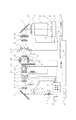
図3は本発明の特徴を最もよく表す図面であり、同図において66aは固定スリット、66bは露光ムラ調整手段であるところの薄肉金属板(弾性変形が可能な部材であれば他の部材でも構わない)からなる可変スリット、66cは可変スリットのスリット方向に局所的に取り付けられたコマ、66dはコマ受け、66eは回動案内機構、66f及び66gは互いに直交する直動案内機構で構成された平面案内機構である。仮に、中央の駆動軸に平面案内機構を設けると、可変スリットの該平面内位置が定まらないため、中央の駆動軸には平面案内機構を設けない。 FIG. 3 is a drawing that best represents the features of the present invention, in which 66a is a fixed slit and 66b is a non-uniform exposure adjusting means, which is a thin metal plate (other members can be elastically deformed). 66c is a frame locally attached in the slit direction of the variable slit, 66d is a frame receiver, 66e is a rotation guide mechanism, and 66f and 66g are linear motion guide mechanisms orthogonal to each other. It is a flat guide mechanism. If a plane guide mechanism is provided on the central drive shaft, the position of the variable slit in the plane is not determined, and therefore no plane guide mechanism is provided on the central drive shaft.
また、複数ある駆動軸が可変スリット(薄肉金属板)に加える力は、図3、7における上下方向、すなわち、照明光学系の光軸に対して実質的に垂直な方向(照明光学系が形成するスリットの幅方向、レチクルやウエハ上でのスキャン方向に相当する方向)である。但し、複数ある駆動軸が可変スリットに対して与える力(変位)の方向が同じであれば、照明光学系の光軸に対して傾いた方向の力を可変スリットに対して与えるような構成としても構わない。 Further, the force applied to the variable slit (thin metal plate) by a plurality of drive shafts is the vertical direction in FIGS. 3 and 7, that is, the direction substantially perpendicular to the optical axis of the illumination optical system (formed by the illumination optical system). And the direction corresponding to the scanning direction on the reticle or wafer). However, if the direction of the force (displacement) applied to the variable slit by the plurality of drive shafts is the same, a configuration in which a force in a direction inclined with respect to the optical axis of the illumination optical system is applied to the variable slit is adopted. It doesn't matter.
ここでは、中央の駆動軸には平面案内機構を設けずに、回動案内機構を設けているが、中央の駆動軸には回動案内機構も設けないようにしても構わない。つまり、中央の駆動軸には平面案内機構も回動案内機構も設けず、中央の駆動軸によって、可変スリットの薄肉金属板の中央部の位置及び照明光学系の光軸に対する傾きを決定するような構成としても構わない。 Here, the center drive shaft is not provided with the plane guide mechanism, but the rotation guide mechanism is provided. However, the center drive shaft may not be provided with the rotation guide mechanism. That is, the central drive shaft is not provided with a plane guide mechanism or a rotation guide mechanism, and the central drive shaft determines the position of the central portion of the thin metal plate of the variable slit and the inclination of the illumination optical system with respect to the optical axis. It does not matter even if it is a simple configuration.
勿論、このように平面案内機構を設けない駆動軸は中央である必要は無く、可変スリットをスキャン方向(レチクル上でのスキャン方向、レチクル上におけるスリットの幅方向)に押し引きする複数の駆動軸のうちいずれか1つであれば良い。また、本実施例においては、1つの駆動軸に対して1つの回動案内機構と2つの平面案内機構とを設けているが、2つの平面案内機構を2次元的な案内機構に置き換えたり、1つの回動案内機構と1つの平面案内機構の代わりに平面内に拘束するような案内機構(例えば板バネ等)を用いたりしても構わない。 Of course, the drive shaft without the planar guide mechanism need not be in the center, and a plurality of drive shafts that push and pull the variable slit in the scan direction (scan direction on the reticle, width direction of the slit on the reticle). Any one of them may be used. In this embodiment, one rotation guide mechanism and two plane guide mechanisms are provided for one drive shaft. However, the two plane guide mechanisms may be replaced with a two-dimensional guide mechanism, Instead of one rotation guide mechanism and one plane guide mechanism, a guide mechanism (for example, a leaf spring) that restrains in a plane may be used.
上記構成において、複数のアクチュエータが押し引き運動を起こすと、可変スリット66bが撓むことにより板の厚さの方向へ変形する。このとき、回動案内機構66eと平面案内機構66f、66gが運動することにより、可変スリットの変形に不要な応力が該案内機構に散逸される。したがって、アクチュエータの負荷は最低限に抑えられ、可変スリットと66bを形成している薄肉金属板が塑性変形する危険性も大幅に削減できる。
In the above configuration, when a plurality of actuators cause a pulling and pulling motion, the
本実施例は、図8(A)の矩形の露光領域82内部にある略平行の最大開口エリア83を利用している。開口エリア84はスリットの初期開口形状を表している。
In this embodiment, a substantially parallel maximum opening area 83 inside the rectangular exposure area 82 in FIG. 8A is used. The
以上の作用により、ウェハ面上での照度ムラに基き、露光ムラ調整スリット機構の開口幅を最大開口エリア83の範囲内で局所的に変えることにより、スキャン露光したときのウェハ面上での積算露光量を実質的に均一に保つことが可能になる。 Based on the illuminance unevenness on the wafer surface by the above operation, the opening width of the exposure unevenness adjustment slit mechanism is locally changed within the range of the maximum opening area 83, so that integration on the wafer surface at the time of scan exposure is performed. The exposure amount can be kept substantially uniform.
ここで、ウエハ25面上での積算露光量は、ウエハを載置するウエハステージ(ウエハを搭載して移動可能な部位)上に設けられた照度むらセンサ(光量センサ)27を用いて測定し、その結果を受けた主制御系9が前記アクチュエータの押し引き運動を制御することによって、スリットの長さ方向(スリット方向)の複数箇所におけるスリット幅の調整を行っている。ここで照度むらセンサを用いてウエハ上での光量測定は、ウエハをスキャン方向に一度露光する度、ウエハをスキャン方向に1往復露光する度、ウエハを1枚露光し終わる度、ウエハを1ロット露光し終わる度、もしくはウエハの焼付けに異常な兆候が見られる度に行う。
Here, the integrated exposure amount on the surface of the
また、必要に応じてスリットを実質的に閉じてしまうことも可能である。 It is also possible to close the slit substantially as necessary.
また、前記露光領域整形手段すなわち露光ムラ調整スリット機構の可変スリットは、可撓性のある薄肉金属板で形成されており、該薄肉金属板のエッジ中央においてスリット方向を回転軸として回転傾斜した位置に配置されている。 The exposure area shaping means, that is, the variable slit of the exposure unevenness adjusting slit mechanism is formed of a flexible thin metal plate, and is a position that is rotated and inclined with the slit direction as a rotation axis at the edge center of the thin metal plate. Is arranged.
この可変スリットを押し引きする機構の動作方向はスキャン方向であり、該機構が前記ブラインド機構と干渉することはない。該可変スリットの変形方向は該スリットを形成している前記薄肉金属板の厚さ方向に平行である。 The operating direction of the mechanism that pushes and pulls the variable slit is the scanning direction, and the mechanism does not interfere with the blind mechanism. The deformation direction of the variable slit is parallel to the thickness direction of the thin metal plate forming the slit.
前記可変スリットを押し引きする機構の動作方向を該可変スリットの変形方向へ変換するために、前記薄肉金属板の複数箇所で取り付けられた部材に、スリット方向と可変スリットの変形方向に直交する方向を回転軸とする回動案内機構を設け、さらに中央の押し引き機構には該回動案内機構だけを設け、その他の押し引き機構には該回動機構に加えてスリット方向と光軸方向へスライドする平面案内機構を設けることが望ましい。 A direction orthogonal to the slit direction and the deformation direction of the variable slit on a member attached at a plurality of locations on the thin metal plate in order to convert the operation direction of the mechanism for pushing and pulling the variable slit into the deformation direction of the variable slit. A rotation guide mechanism with the rotation axis as the rotation axis is provided, and the center push-pull mechanism is provided with only the rotation guide mechanism, and the other push-pull mechanisms are provided in the slit direction and the optical axis direction in addition to the rotation mechanism. It is desirable to provide a plane guide mechanism that slides.
また、前記露光ムラ調整スリット機構は、スリットの開口形状が略平行あるいは円弧の両方の場合に適用できる。また、前記露光ムラ調整スリット機構は、可変スリットを形成している薄肉金属板に無理な応力が発生しようとも、前記回動案内機構と前記平面案内機構が運動することにより、可変スリットの変形に不要な応力が該案内機構へ散逸するために、アクチュエータの負荷が最低限に抑えられ、可変スリットを形成している薄肉金属板が塑性変形する危険性も大幅に削減できる。 Further, the exposure unevenness adjusting slit mechanism can be applied when the opening shape of the slit is substantially parallel or circular. Further, the exposure unevenness adjusting slit mechanism is capable of deforming the variable slit by moving the rotation guide mechanism and the plane guide mechanism even if an excessive stress is generated on the thin metal plate forming the variable slit. Since unnecessary stress is dissipated to the guide mechanism, the load on the actuator is minimized, and the risk of plastic deformation of the thin metal plate forming the variable slit can be greatly reduced.
本実施例2が実施例1と異なる点は、実施例1では略平行スリットを前提としていたが、実施例2では露光ムラ調整スリット機構はカタディオ投影系における円弧スリットの開口幅を局所的に変更する場合に適用している点である。その他、実施例2で特に記載していない部分に関しては実施例1と同様である。 The difference between the second embodiment and the first embodiment is that a substantially parallel slit is assumed in the first embodiment. However, in the second embodiment, the exposure unevenness adjusting slit mechanism locally changes the opening width of the arc slit in the catadiographic projection system. It is a point that is applied when doing. Other parts not specifically described in the second embodiment are the same as those in the first embodiment.
実施例2においては、円弧スリットは楕円柱表面に薄肉金属板を馴染ませて加工製造し、該楕円柱の軸に対して全体を斜めにスライスすることにより、薄肉金属板のエッジ形状を円弧状にしている。 In Example 2, the arc slit is manufactured by making the thin metal plate fit on the surface of the elliptical cylinder, and the entire shape is sliced obliquely with respect to the axis of the elliptical cylinder so that the edge shape of the thin metal plate is an arc shape. I have to.
図4は本発明の特徴を最もよく表す図面であり、同図において66aは固定スリット、66bは露光ムラ調整手段であるところの薄肉金属板からなる可変スリット、66cは可変スリットのスリット方向に局所的に取り付けられたコマ、66dはコマ受け、66eは回動案内機構、66f及び66gは互いに直交する直動案内機構で構成された平面案内機構である。仮に、中央の駆動軸に平面案内機構を設けると、可変スリットの該平面内位置が定まらないため、中央の駆動軸には平面案内機構を設けない。 FIG. 4 is a drawing that best represents the features of the present invention, in which 66a is a fixed slit, 66b is a variable slit made of a thin metal plate serving as exposure unevenness adjusting means, and 66c is locally located in the slit direction of the variable slit. A top frame, 66d is a frame support, 66e is a rotation guide mechanism, and 66f and 66g are plane guide mechanisms composed of linear motion guide mechanisms orthogonal to each other. If a plane guide mechanism is provided on the central drive shaft, the position of the variable slit in the plane is not determined, and therefore no plane guide mechanism is provided on the central drive shaft.
ここでは、中央の駆動軸には平面案内機構を設けずに、回動案内機構を設けているが、中央の駆動軸には回動案内機構も設けないようにしても構わない。つまり、中央の駆動軸には平面案内機構も回動案内機構も設けず、中央の駆動軸によって、可変スリットの薄肉金属板の中央部の位置及び照明光学系の光軸に対する傾きを決定するような構成としても構わない。 Here, the center drive shaft is not provided with the plane guide mechanism, but the rotation guide mechanism is provided. However, the center drive shaft may not be provided with the rotation guide mechanism. That is, the central drive shaft is not provided with a plane guide mechanism or a rotation guide mechanism, and the central drive shaft determines the position of the central portion of the thin metal plate of the variable slit and the inclination of the illumination optical system with respect to the optical axis. It does not matter even if it is a simple configuration.
勿論、このように平面案内機構を設けない駆動軸は中央である必要は無く、可変スリットをスキャン方向(レチクル上でのスキャン方向、レチクル上におけるスリットの幅方向)に押し引きする複数の駆動軸のうちいずれか1つであれば良い。また、本実施例においては、1つの駆動軸に対して1つの回動案内機構と2つの平面案内機構とを設けているが、2つの平面案内機構を2次元的な案内機構に置き換えたり、1つの回動案内機構と1つの平面案内機構の代わりに平面内に拘束するような案内機構(例えば板バネ等)を用いたりしても構わない。 Of course, the drive shaft without the planar guide mechanism need not be in the center, and a plurality of drive shafts that push and pull the variable slit in the scan direction (scan direction on the reticle, width direction of the slit on the reticle). Any one of them may be used. In this embodiment, one rotation guide mechanism and two plane guide mechanisms are provided for one drive shaft. However, the two plane guide mechanisms may be replaced with a two-dimensional guide mechanism, Instead of one rotation guide mechanism and one plane guide mechanism, a guide mechanism (for example, a leaf spring) that restrains in a plane may be used.
上記構成において、複数のアクチュエータが押し引き運動を起こすと、可変スリット66bが撓むことにより板の厚さの方向へ変形する。このとき、回動案内機構66eと平面案内機構66f、66gが運動することにより、可変スリットの変形に不要な応力が該案内機構に散逸される。したがって、アクチュエータの負荷は最低限に抑えられ、可変スリットと66bを形成している薄肉金属板が塑性変形する危険性も大幅に削減できる。
In the above configuration, when a plurality of actuators cause a pulling and pulling motion, the
図8(B)は投影レンズ22のウエハ25上の有効領域を示すものであるが、投影レンズ22は一般的に外周が円形の光学素子の組み合わせによって成り立っているために、レンズ自体では円形の有効部81を有しているが、前述したように、スリットスキャン方式の露光装置では広い幅でスキャン露光を行うためにレンズの有効部81の中で、矩形の露光領域82を使用している。本実施例は、投影光学系にエネルギー効率、色収差、対環境敏感度の点から光学系内に複数のミラーとレンズを配置したカタディオプトリックタイプを選択し、スリットの開口形状が円弧状であるスキャニング式投影露光装置に適用させるものであるため、矩形の露光領域82内部にある円弧状の最大開口エリア83を利用している。開口エリア84はスリットの初期開口形状を表している。
FIG. 8B shows the effective area of the
以上の作用により、ウェハ面上での照度ムラに基き、露光ムラ調整スリット機構の開口幅を最大開口エリア83の範囲内で局所的に変えることにより、スキャン露光したときのウェハ面上での積算露光量を実質的に均一に保つことが可能になる。 Based on the illuminance unevenness on the wafer surface by the above operation, the opening width of the exposure unevenness adjustment slit mechanism is locally changed within the range of the maximum opening area 83, so that integration on the wafer surface at the time of scan exposure is performed. The exposure amount can be kept substantially uniform.
ここで、ウエハ25面上での積算露光量は、ウエハを載置するウエハステージ(ウエハを搭載して移動可能な部位)上に設けられた照度むらセンサ(光量センサ)27を用いて測定し、その結果を受けた主制御系9が前記アクチュエータの押し引き運動を制御することによって、スリットの長さ方向(スリット方向)の複数箇所におけるスリット幅の調整を行っている。ここで照度むらセンサを用いてウエハ上での光量測定は、ウエハをスキャン方向に一度露光する度、ウエハをスキャン方向に1往復露光する度、ウエハを1枚露光し終わる度、ウエハを1ロット露光し終わる度、もしくはウエハの焼付けに異常な兆候が見られる度に行う。
Here, the integrated exposure amount on the surface of the
また、必要に応じてスリットを実質的に閉じてしまうことも可能である。 It is also possible to close the slit substantially as necessary.
次に上記説明した投影露光装置を利用したデバイスの生産方法の実施例3を説明する。図11は微小デバイス(ICやLSI等の半導体チップ、液晶パネル、CCD、薄膜磁気ヘッド、マイクロマシン等)の製造のフローを示す。ステップ1(回路設計)ではデバイスのパターン設計を行う。ステップ2(マスク製作)では設計したパターンを形成したマスクを製作する。一方、ステップ3(ウエハ製造)ではシリコンやガラス等の材料を用いてウエハを製造する。ステップ4(ウエハプロセス)は前工程と呼ばれ、上記用意したマスクとウエハを用いて、リソグラフィ技術によってウエハ上に実際の回路を形成する。次のステップ5(組み立て)は後工程と呼ばれ、ステップ4によって作製されたウエハを用いて半導体チップ化する工程であり、アッセンブリ工程(ダイシング、ボンディング)、パッケージング工程(チップ封入)等の工程を含む。ステップ6(検査)ではステップ5で作製された半導体デバイスの動作確認テスト、耐久性テスト等の検査を行なう。こうした工程を経て半導体デバイスが完成し、これが出荷(ステップ7)される。 Next, a third embodiment of the device production method using the above-described projection exposure apparatus will be described. FIG. 11 shows a flow of manufacturing a microdevice (a semiconductor chip such as an IC or LSI, a liquid crystal panel, a CCD, a thin film magnetic head, a micromachine, etc.). In step 1 (circuit design), a device pattern is designed. In step 2 (mask production), a mask on which the designed pattern is formed is produced. On the other hand, in step 3 (wafer manufacture), a wafer is manufactured using a material such as silicon or glass. Step 4 (wafer process) is called a pre-process, and an actual circuit is formed on the wafer by lithography using the prepared mask and wafer. The next step 5 (assembly) is referred to as a post-process, and is a process for forming a semiconductor chip using the wafer produced in step 4, such as an assembly process (dicing, bonding), a packaging process (chip encapsulation), and the like. including. In step 6 (inspection), inspections such as an operation confirmation test and a durability test of the semiconductor device manufactured in step 5 are performed. Through these steps, the semiconductor device is completed and shipped (step 7).
図12は上記ウエハプロセスの詳細なフローを示す。ステップ11(酸化)ではウエハの表面を酸化させる。ステップ12(CVD)ではウエハ表面に絶縁膜を形成する。ステップ13(電極形成)ではウエハ上に電極を蒸着によって形成する。ステップ14(イオン打込み)ではウエハにイオンを打ち込む。ステップ15(レジスト処理)ではウエハに感光剤を塗布する。ステップ16(露光)では上記説明した投影露光装置によってマスクの回路パターンをウエハに焼付露光する。ステップ17(現像)では露光したウエハを現像する。ステップ18(エッチング)では現像したレジスト像以外の部分を削り取る。ステップ19(レジスト剥離)ではエッチングが済んで不要となったレジストを取り除く。これらのステップを繰り返し行うことによって、ウエハ上に多重に回路パターンが形成される。 FIG. 12 shows a detailed flow of the wafer process. In step 11 (oxidation), the wafer surface is oxidized. In step 12 (CVD), an insulating film is formed on the wafer surface. In step 13 (electrode formation), an electrode is formed on the wafer by vapor deposition. In step 14 (ion implantation), ions are implanted into the wafer. In step 15 (resist process), a photosensitive agent is applied to the wafer. In step 16 (exposure), the circuit pattern of the mask is printed on the wafer by exposure using the projection exposure apparatus described above. In step 17 (development), the exposed wafer is developed. In step 18 (etching), portions other than the developed resist image are removed. In step 19 (resist stripping), unnecessary resist after etching is removed. By repeatedly performing these steps, multiple circuit patterns are formed on the wafer.
本実施例の生産方法を用いれば、従来は製造が難しかった高集積度のデバイスを低コストに製造することができる。 By using the production method of this embodiment, a highly integrated device that has been difficult to manufacture can be manufactured at low cost.
以上のように、本実施例によれば、前記露光ムラ調整スリット機構は、略平行スリットにも円弧スリットにも適用でき、可変スリットを形成している薄肉金属板に無理な応力が発生しようとも、前記回動案内機構と前記平面案内機構が運動することにより、可変スリットの変形に不要な応力が該案内機構へ散逸するために、アクチュエータの負荷が最低限に抑えられ、可変スリットを形成している薄肉金属板が塑性変形する危険性も大幅に削減できる。 As described above, according to this embodiment, the exposure unevenness adjusting slit mechanism can be applied to both a substantially parallel slit and an arc slit, and even if an excessive stress is generated on the thin metal plate forming the variable slit. Since the rotation guide mechanism and the planar guide mechanism move, stress unnecessary for deformation of the variable slit is dissipated to the guide mechanism, so that the load on the actuator is minimized and the variable slit is formed. The risk of plastic deformation of the thin metal plate can be greatly reduced.
また、投影露光装置の構造から鑑みて、前記スリットのエッジ近傍のマスク共役面には、マスクの照射領域を制限するブラインド機構が配置されているが、押し引き機構が光軸方向とスリット方向に直交する方向に収められるため、露光ムラ調整スリット機構と該ブラインド機構との干渉は避けられる。 In view of the structure of the projection exposure apparatus, a blind mechanism for limiting the irradiation area of the mask is arranged on the mask conjugate surface near the edge of the slit, but the push / pull mechanism is arranged in the optical axis direction and the slit direction. Since they are stored in the orthogonal direction, interference between the exposure unevenness adjusting slit mechanism and the blind mechanism can be avoided.
1 光源
2 楕円集光ミラー
9 オプティカルインテグレータ
14 オプティカルインテグレータ
22 投影レンズ
23 マスク(原版)
25 ウェハ(感光基板)
32 可動ブラインド
33 調整ブラインド(露光領域整形手段を調整する)
34 固定ブラインド
51 駆動点
60 開口エリア
66 遮光板
81 円形の有効部
82 矩形の露光領域
83 最大開口エリア
84 開口エリア
91 電源
92 露光量制御系
94 主制御系
95 ステージ制御系
96 露光範囲制御系
DESCRIPTION OF SYMBOLS 1 Light source 2 Elliptical condensing mirror 9
25 wafer (photosensitive substrate)
32 movable blind 33 adjustment blind (adjusting exposure area shaping means)
34 fixed blind 51
Claims (6)
前記照明光学系は、前記被照明面と共役な位置の近傍に配置された、開口幅が可変な開口可変機構を有し、
該開口可変機構が、一枚の遮光板と、該一枚の遮光板の複数箇所に対して力を加えるために、前記マスクと前記基板との相対移動の方向に対応する方向の駆動軸を有する複数の駆動機構とを含み、
該複数の駆動機構のうちの少なくとも1つの駆動機構が、1つの回動案内機構と、前記駆動軸に垂直な2軸方向に関する平面案内機構とを有することを特徴とする露光装置。 An exposure apparatus having an illumination optical system that illuminates a mask disposed on an illuminated surface using light from a light source, and projects the mask pattern onto the substrate by relatively moving the mask and the substrate In
The illumination optical system, the located in the vicinity of the surface to be illuminated and a position conjugate with the aperture width has a variable aperture varying mechanism,
Opening the variable mechanism includes a single light shielding plate, in order to apply a force against the plurality of positions of a single light shielding plate said, the direction of the drive shaft corresponding to the direction of relative movement of the said mask substrate A plurality of drive mechanisms having ,
At least one drive mechanism of the plurality of drive mechanisms, one and the turning guide mechanism, the exposure is characterized that you have a a planar guide mechanism about two vertically axial to the drive shaft unit.
Priority Applications (2)
| Application Number | Priority Date | Filing Date | Title |
|---|---|---|---|
| JP2003434549A JP4458329B2 (en) | 2003-12-26 | 2003-12-26 | Exposure apparatus and device manufacturing method |
| US11/019,106 US7148948B2 (en) | 2003-12-26 | 2004-12-22 | Scanning exposure apparatus, and device manufacturing method |
Applications Claiming Priority (1)
| Application Number | Priority Date | Filing Date | Title |
|---|---|---|---|
| JP2003434549A JP4458329B2 (en) | 2003-12-26 | 2003-12-26 | Exposure apparatus and device manufacturing method |
Publications (3)
| Publication Number | Publication Date |
|---|---|
| JP2005191495A JP2005191495A (en) | 2005-07-14 |
| JP2005191495A5 JP2005191495A5 (en) | 2007-02-08 |
| JP4458329B2 true JP4458329B2 (en) | 2010-04-28 |
Family
ID=34791591
Family Applications (1)
| Application Number | Title | Priority Date | Filing Date |
|---|---|---|---|
| JP2003434549A Expired - Fee Related JP4458329B2 (en) | 2003-12-26 | 2003-12-26 | Exposure apparatus and device manufacturing method |
Country Status (2)
| Country | Link |
|---|---|
| US (1) | US7148948B2 (en) |
| JP (1) | JP4458329B2 (en) |
Families Citing this family (10)
| Publication number | Priority date | Publication date | Assignee | Title |
|---|---|---|---|---|
| JP2007158225A (en) * | 2005-12-08 | 2007-06-21 | Canon Inc | Aligner |
| JP2010123755A (en) | 2008-11-19 | 2010-06-03 | Canon Inc | Exposure apparatus, and device manufacturing method |
| US9494463B2 (en) * | 2009-05-07 | 2016-11-15 | Thermo Scientific Portable Analytical Instruments Inc. | Optical emission spectroscopic (OES) instrument with automatic top and bottom slit curtains |
| JP5127875B2 (en) | 2010-04-28 | 2013-01-23 | キヤノン株式会社 | Lithographic apparatus and article manufacturing method |
| NL2007367A (en) | 2010-11-01 | 2012-05-02 | Asml Netherlands Bv | Lithographic apparatus and method. |
| JP6642969B2 (en) * | 2015-02-16 | 2020-02-12 | キヤノン株式会社 | Optical unit, image forming apparatus, and method of manufacturing optical unit |
| JP6506599B2 (en) * | 2015-04-15 | 2019-04-24 | キヤノン株式会社 | Illumination optical system, exposure apparatus and device manufacturing method |
| JP6570298B2 (en) * | 2015-04-15 | 2019-09-04 | キヤノン株式会社 | Illumination optical system, exposure apparatus, and device manufacturing method |
| JP6626273B2 (en) * | 2015-06-03 | 2019-12-25 | キヤノン株式会社 | Exposure apparatus and article manufacturing method |
| DE102016208174A1 (en) * | 2016-05-12 | 2017-04-27 | Carl Zeiss Smt Gmbh | OPTICAL SYSTEM, IN PARTICULAR LITHOGRAPHIC PLANT, AND METHOD |
Family Cites Families (10)
| Publication number | Priority date | Publication date | Assignee | Title |
|---|---|---|---|---|
| US4822975A (en) | 1984-01-30 | 1989-04-18 | Canon Kabushiki Kaisha | Method and apparatus for scanning exposure |
| JPS60158449A (en) | 1984-01-30 | 1985-08-19 | Canon Inc | Exposing device |
| JPS62193125A (en) | 1986-02-19 | 1987-08-25 | Canon Inc | Exposure-uneveness correcting apparatus |
| US5777724A (en) | 1994-08-24 | 1998-07-07 | Suzuki; Kazuaki | Exposure amount control device |
| JP3348928B2 (en) | 1993-08-26 | 2002-11-20 | 株式会社ニコン | Scanning exposure method, scanning type exposure apparatus, and exposure amount control apparatus |
| JPH1050599A (en) | 1996-08-05 | 1998-02-20 | Nikon Corp | Method for controlling aligner |
| US6538723B2 (en) | 1996-08-05 | 2003-03-25 | Nikon Corporation | Scanning exposure in which an object and pulsed light are moved relatively, exposing a substrate by projecting a pattern on a mask onto the substrate with pulsed light from a light source, light sources therefor, and methods of manufacturing |
| US6013401A (en) * | 1997-03-31 | 2000-01-11 | Svg Lithography Systems, Inc. | Method of controlling illumination field to reduce line width variation |
| JP4392879B2 (en) | 1998-09-28 | 2010-01-06 | キヤノン株式会社 | Projection exposure apparatus and device manufacturing method |
| JP2001244183A (en) | 2000-02-29 | 2001-09-07 | Canon Inc | Projection exposure system |
-
2003
- 2003-12-26 JP JP2003434549A patent/JP4458329B2/en not_active Expired - Fee Related
-
2004
- 2004-12-22 US US11/019,106 patent/US7148948B2/en active Active
Also Published As
| Publication number | Publication date |
|---|---|
| US20050162628A1 (en) | 2005-07-28 |
| JP2005191495A (en) | 2005-07-14 |
| US7148948B2 (en) | 2006-12-12 |
Similar Documents
| Publication | Publication Date | Title |
|---|---|---|
| TW546699B (en) | Exposure apparatus and exposure method capable of controlling illumination distribution | |
| JP2011040716A (en) | Exposure apparatus, exposure method, and device manufacturing method | |
| JP3799275B2 (en) | Scanning exposure apparatus, manufacturing method thereof, and device manufacturing method | |
| JP2006245157A (en) | Exposure method and device | |
| JP4458329B2 (en) | Exposure apparatus and device manufacturing method | |
| US20040157143A1 (en) | Exposure method and lithography system, exposure apparatus and method of making the apparatus, and method of manufacturing device | |
| JP5387982B2 (en) | Illumination optical apparatus, exposure apparatus, and device manufacturing method | |
| JP2001244183A (en) | Projection exposure system | |
| JP4684563B2 (en) | Exposure apparatus and method | |
| JP2006120798A (en) | Exposure apparatus | |
| JP4764161B2 (en) | Exposure apparatus, exposure method, and device manufacturing method | |
| CN107783383B (en) | Exposure apparatus, exposure method, and article manufacturing method | |
| JP4838698B2 (en) | Exposure apparatus and device manufacturing method | |
| JP2006261418A (en) | Projection aligner and process for fabricating device | |
| JP2004226661A (en) | Method for forming three-dimensional structure | |
| JP2005085991A (en) | Exposure apparatus and manufacturing method of device using the apparatus | |
| JP4235410B2 (en) | Exposure method | |
| JP2009164356A (en) | Scanning exposure device and device manufacturing method | |
| JP2011086708A (en) | Diaphragm device, optical system, exposure device, and method of manufacturing electronic device | |
| JP4298305B2 (en) | Exposure apparatus and semiconductor device manufacturing method | |
| JP2001338866A (en) | Aligner, method for manufacturing device, and method for measuring accuracy in aligner | |
| EP0831376A2 (en) | Scanning exposure method and mask therefor | |
| US20070072128A1 (en) | Method of manufacturing an integrated circuit to obtain uniform exposure in a photolithographic process | |
| TWI711893B (en) | Exposure apparatus, manufacturing method of flat panel display, and device manufacturing method | |
| JP5539293B2 (en) | Exposure apparatus and device manufacturing method |
Legal Events
| Date | Code | Title | Description |
|---|---|---|---|
| A521 | Request for written amendment filed |
Free format text: JAPANESE INTERMEDIATE CODE: A523 Effective date: 20061218 |
|
| A621 | Written request for application examination |
Free format text: JAPANESE INTERMEDIATE CODE: A621 Effective date: 20061218 |
|
| A977 | Report on retrieval |
Free format text: JAPANESE INTERMEDIATE CODE: A971007 Effective date: 20090916 |
|
| A131 | Notification of reasons for refusal |
Free format text: JAPANESE INTERMEDIATE CODE: A131 Effective date: 20090924 |
|
| A521 | Request for written amendment filed |
Free format text: JAPANESE INTERMEDIATE CODE: A523 Effective date: 20091124 |
|
| TRDD | Decision of grant or rejection written | ||
| A01 | Written decision to grant a patent or to grant a registration (utility model) |
Free format text: JAPANESE INTERMEDIATE CODE: A01 Effective date: 20100126 |
|
| A01 | Written decision to grant a patent or to grant a registration (utility model) |
Free format text: JAPANESE INTERMEDIATE CODE: A01 |
|
| RD04 | Notification of resignation of power of attorney |
Free format text: JAPANESE INTERMEDIATE CODE: A7424 Effective date: 20100201 |
|
| A61 | First payment of annual fees (during grant procedure) |
Free format text: JAPANESE INTERMEDIATE CODE: A61 Effective date: 20100203 |
|
| R150 | Certificate of patent or registration of utility model |
Free format text: JAPANESE INTERMEDIATE CODE: R150 Ref document number: 4458329 Country of ref document: JP Free format text: JAPANESE INTERMEDIATE CODE: R150 |
|
| FPAY | Renewal fee payment (event date is renewal date of database) |
Free format text: PAYMENT UNTIL: 20130219 Year of fee payment: 3 |
|
| FPAY | Renewal fee payment (event date is renewal date of database) |
Free format text: PAYMENT UNTIL: 20140219 Year of fee payment: 4 |
|
| LAPS | Cancellation because of no payment of annual fees |