JP4383408B2 - Lithographic apparatus and device fabrication method - Google Patents
Lithographic apparatus and device fabrication method Download PDFInfo
- Publication number
- JP4383408B2 JP4383408B2 JP2005375770A JP2005375770A JP4383408B2 JP 4383408 B2 JP4383408 B2 JP 4383408B2 JP 2005375770 A JP2005375770 A JP 2005375770A JP 2005375770 A JP2005375770 A JP 2005375770A JP 4383408 B2 JP4383408 B2 JP 4383408B2
- Authority
- JP
- Japan
- Prior art keywords
- layer
- final element
- substrate
- liquid
- projection system
- Prior art date
- Legal status (The legal status is an assumption and is not a legal conclusion. Google has not performed a legal analysis and makes no representation as to the accuracy of the status listed.)
- Expired - Fee Related
Links
Images


Classifications
-
- G—PHYSICS
- G03—PHOTOGRAPHY; CINEMATOGRAPHY; ANALOGOUS TECHNIQUES USING WAVES OTHER THAN OPTICAL WAVES; ELECTROGRAPHY; HOLOGRAPHY
- G03F—PHOTOMECHANICAL PRODUCTION OF TEXTURED OR PATTERNED SURFACES, e.g. FOR PRINTING, FOR PROCESSING OF SEMICONDUCTOR DEVICES; MATERIALS THEREFOR; ORIGINALS THEREFOR; APPARATUS SPECIALLY ADAPTED THEREFOR
- G03F7/00—Photomechanical, e.g. photolithographic, production of textured or patterned surfaces, e.g. printing surfaces; Materials therefor, e.g. comprising photoresists; Apparatus specially adapted therefor
- G03F7/70—Microphotolithographic exposure; Apparatus therefor
- G03F7/70216—Mask projection systems
- G03F7/70341—Details of immersion lithography aspects, e.g. exposure media or control of immersion liquid supply
-
- G—PHYSICS
- G03—PHOTOGRAPHY; CINEMATOGRAPHY; ANALOGOUS TECHNIQUES USING WAVES OTHER THAN OPTICAL WAVES; ELECTROGRAPHY; HOLOGRAPHY
- G03F—PHOTOMECHANICAL PRODUCTION OF TEXTURED OR PATTERNED SURFACES, e.g. FOR PRINTING, FOR PROCESSING OF SEMICONDUCTOR DEVICES; MATERIALS THEREFOR; ORIGINALS THEREFOR; APPARATUS SPECIALLY ADAPTED THEREFOR
- G03F7/00—Photomechanical, e.g. photolithographic, production of textured or patterned surfaces, e.g. printing surfaces; Materials therefor, e.g. comprising photoresists; Apparatus specially adapted therefor
- G03F7/70—Microphotolithographic exposure; Apparatus therefor
- G03F7/708—Construction of apparatus, e.g. environment aspects, hygiene aspects or materials
- G03F7/7095—Materials, e.g. materials for housing, stage or other support having particular properties, e.g. weight, strength, conductivity, thermal expansion coefficient
- G03F7/70958—Optical materials or coatings, e.g. with particular transmittance, reflectance or anti-reflection properties
Description
本発明は、リソグラフィ機器及びデバイスを製作する方法に関する。 The present invention relates to a lithographic apparatus and a method for manufacturing a device.
リソグラフィ機器は、基板に、通常は基板の目標部分に所望のパターンを適用する機械である。リソグラフィ機器は、例えば、集積回路(IC)の製作で使用することができる。この場合には、マスク又はレチクルとも称するパターン化装置を使用して、ICの個々の層に形成すべき回路パターンを生成し得る。このパターンは、基板(例えばシリコン・ウエハ)の(例えば、ダイの一部或いは1つ又は複数のダイを含む)目標部分に転写することができる。パターンの転写は、典型的には、基板上に形成された放射感受性材料(レジスト)の層への結像を介して行われる。一般に、1枚の基板は、次々にパターン化される隣接した網目状の目標部分を含む。周知のリソグラフィ機器の例は、目標部分にパターン全体を1回露光することによって各目標部分が照射されるいわゆるステッパと、所与の方向(「走査」方向)に放射ビームを通過してパターンを走査し、この方向と平行又は逆平行に基板を同期走査することによって各目標部分が照射されるいわゆるスキャナである。基板上にパターンをインプリントすることによって、パターン化装置から基板にパターンを転写することも可能である。 A lithographic apparatus is a machine that applies a desired pattern onto a substrate, usually onto a target portion of the substrate. A lithographic apparatus can be used, for example, in the manufacture of integrated circuits (ICs). In this case, a patterning device, also referred to as a mask or reticle, may be used to generate circuit patterns to be formed on individual layers of the IC. This pattern can be transferred onto a target portion (eg including part of, one, or several dies) on a substrate (eg a silicon wafer). Pattern transfer is typically done via imaging onto a layer of radiation sensitive material (resist) formed on the substrate. In general, a single substrate will contain a network of adjacent target portions that are successively patterned. An example of a known lithographic apparatus is a so-called stepper in which each target portion is irradiated by exposing the entire pattern once to the target portion, and a pattern passing through the radiation beam in a given direction (the “scan” direction). This is a so-called scanner in which each target portion is irradiated by scanning and synchronously scanning the substrate in parallel or antiparallel to this direction. It is also possible to transfer the pattern from the patterning device to the substrate by imprinting the pattern onto the substrate.
リソグラフィ投影機器内で、比較的高屈折率の液体、例えば水に基板を浸して、投影系の最終要素と基板の間のスペースを満たすことが提案されている。この趣旨は、液体中では露光放射の波長がより短くなるので、より小さなフィーチャを結像し得ることである(液体の作用は、系の実効NAを大きくし、焦点深度も深くすることとみなすこともできる)。固体粒子(例えば、石英)が浮遊する水を含めて、他の浸漬液が提案されている。248nm又は193nmの投影放射には水又は水溶液、157nmの投影放射にはパーフルオロ炭化水素(perfluorohydrocarbon)が提案されている。 In lithographic projection equipment, it has been proposed to immerse the substrate in a relatively high refractive index liquid, such as water, to fill the space between the final element of the projection system and the substrate. The idea is that the wavelength of the exposure radiation is shorter in the liquid, so that smaller features can be imaged (the action of the liquid is considered to increase the effective NA of the system and increase the depth of focus). Can also). Other immersion liquids have been proposed, including water in which solid particles (eg, quartz) are suspended. Water or aqueous solutions have been proposed for 248 nm or 193 nm projection radiation and perfluorohydrocarbon for 157 nm projection radiation.
ただし、基板、又は基板及び基板テーブルを液体の浴の中に浸すこと(例えば、参照により全体をここに組み込む米国特許第4509852号を参照されたい)は、走査露光中に加速しなければならない大きな液体の塊があることを意味する。これは、追加のモータ又はより強力なモータを必要とし、液体中の乱れにより、予測不可能な望ましくない作用が生じることがある。 However, immersing the substrate, or substrate and substrate table, in a bath of liquid (see, eg, US Pat. No. 4,509,852, which is hereby incorporated by reference in its entirety) must be accelerated during a scanning exposure. Means there is a lump of liquid. This requires an additional or more powerful motor, and turbulence in the liquid can cause unpredictable and undesirable effects.
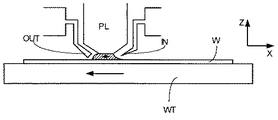
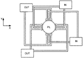
提案されている解決策の1つは、液体供給システムが、投影系の最終要素と基板の間で、基板の局所的な区域にのみ液体を提供することである(基板の表面積は一般に、投影系の最終要素の表面積よりも大きい)。参照により全体をここに組み込むWO 99/49504号に開示されている一方法は、このように構成することを提案している。図2及び図3に示すように、液体は、少なくとも1つの注入口INによって、好ましくは、最終要素に対して相対的に基板の移動方向に沿って基板上に供給され、投影系の下を通過した後で、少なくとも1つの排出口OUTによって取り除かれる。即ち、基板がこの要素の下を−X方向に走査されるとき、液体は、この要素の+X側に供給され、−X側で取り上げられる。図2に、液体が、注入口INを介して供給され、低圧源に接続された排出口OUTによってこの要素の反対側で取り上げられる構成を概略的に示す。図2の例では、液体は、最終要素に対する相対的な基板の移動方向に沿って供給されるが、このようにする必要はない。様々な向き及び数の注入口及び排出口を、最終要素の周りに配置することが可能である。図3に、4組の注入口及び排出口が最終要素の周りを規則的なパターンでどの側にも設けられる一実施例を示す。 One proposed solution is that the liquid supply system provides liquid only to a localized area of the substrate between the final element of the projection system and the substrate (the surface area of the substrate is generally projected). Greater than the surface area of the final element of the system). One method disclosed in WO 99/49504, which is hereby incorporated by reference in its entirety, proposes to do so. As shown in FIGS. 2 and 3, the liquid is supplied onto the substrate by at least one inlet IN, preferably along the direction of movement of the substrate relative to the final element, under the projection system. After passing, it is removed by at least one outlet OUT. That is, when the substrate is scanned under the element in the -X direction, liquid is supplied to the + X side of the element and taken up on the -X side. FIG. 2 schematically shows a configuration in which liquid is supplied via the inlet IN and taken up on the opposite side of this element by an outlet OUT connected to a low pressure source. In the example of FIG. 2, the liquid is supplied along the direction of movement of the substrate relative to the final element, although this need not be the case. Various orientations and numbers of inlets and outlets can be placed around the final element. FIG. 3 shows an embodiment in which four sets of inlets and outlets are provided on either side in a regular pattern around the final element.
したがって、例えば、浸漬液との接触による構成要素の劣化が少ないリソグラフィ投影機器を提供することが有利となろう。 Thus, for example, it would be advantageous to provide a lithographic projection apparatus that has low component degradation due to contact with immersion liquid.
本発明の態様によれば、
基板にパターン化された放射ビームを投影するように構成された投影系を備えるリソグラフィ投影機器であって、この投影系は、基板に最も近い表面上に、この表面に結合した層と、この層と同じ材料の、液体から最終要素を遮蔽するために基板から離れるようにこの層から延びる縁部障壁とを有する最終要素を含み、このリソグラフィ投影機器はさらに、
投影系の最終要素と基板の間のスペースを液体で少なくとも部分的に充填するように構成された液体供給システムを備えるリソグラフィ投影機器が提供される。
According to an aspect of the invention,
A lithographic projection apparatus comprising a projection system configured to project a patterned beam of radiation onto a substrate, the projection system comprising a layer coupled to the surface on a surface closest to the substrate and the layer The lithographic projection apparatus further comprising a final element having the same material and an edge barrier extending from the layer away from the substrate to shield the final element from the liquid.
A lithographic projection apparatus is provided that includes a liquid supply system configured to at least partially fill a space between a final element of a projection system and a substrate with a liquid.
本発明の態様によれば、
基板にパターン化された放射ビームを投影するように構成された投影系を備えるリソグラフィ投影機器であって、この投影系は、基板に最も近い表面上に層を有する最終要素を含み、この最終要素は、この層を介してこの機器に取り付けられ、このリソグラフィ投影機器はさらに、
投影系の最終要素と基板の間のスペースを液体で少なくとも部分的に充填するように構成された液体供給システムを備えるリソグラフィ投影機器が提供される。
According to an aspect of the invention,
A lithographic projection apparatus comprising a projection system configured to project a patterned beam of radiation onto a substrate, the projection system comprising a final element having a layer on a surface closest to the substrate, the final element Is attached to this equipment through this layer, the lithographic projection equipment further comprising:
A lithographic projection apparatus is provided that includes a liquid supply system configured to at least partially fill a space between a final element of a projection system and a substrate with a liquid.
本発明の態様によれば、
投影系の最終要素と基板の間のスペースに設けられた液体を介して、基板にパターン化された放射ビームを投影するステップを含むデバイスの製作方法であって、この最終要素は、基板に最も近い表面上に層を有し、この層を介して最終要素が支持される方法が提供される。
According to an aspect of the invention,
Projecting a patterned radiation beam onto a substrate via a liquid provided in a space between the final element of the projection system and the substrate, the final element being the most on the substrate A method is provided having a layer on a near surface through which the final element is supported.
本発明の態様によれば、
投影系の最終要素と基板の間のスペースに設けられた液体を介して、基板にパターン化された放射ビームを投影するステップを含むデバイスの製作方法であって、基板に最も近い最終要素の表面には層が結合され、この層と同じ材料の縁部障壁が、液体から最終要素を遮蔽するために、基板から離れるようにこの層から延びる方法が提供される。
According to an aspect of the invention,
Projecting a patterned radiation beam onto a substrate via a liquid provided in a space between the final element of the projection system and the substrate, the method of manufacturing the device comprising the surface of the final element closest to the substrate Is provided with a layer bonded and an edge barrier of the same material as this layer extending from this layer away from the substrate to shield the final element from the liquid.
次に、添付の概略図面を参照して、単なる例として本発明の実施例を説明する。図面では、対応する参照記号はそれに対応する部分を示す。 Embodiments of the present invention will now be described by way of example only with reference to the accompanying schematic drawings. In the drawings, corresponding reference symbols indicate corresponding parts.
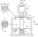
図1に、本発明の一実施例によるリソグラフィ機器を概略的に示す。この機器は、
−放射ビームB(例えば、UV放射又はDUV放射)を調整するように構成された照明系(照明器)ILと、
−パターン化装置(例えば、マスク)MAを支持するように構築された支持構造(例えば、マスク・テーブル)MTであって、ある種のパラメータに従ってパターン化装置を正確に位置決めするように構成された第1位置決め装置PMに結合された支持構造MTと、
−基板(例えば、レジストを塗布したウエハ)Wを保持するように構築された基板テーブル(例えば、ウエハ・テーブル)WTであって、ある種のパラメータに従って基板を正確に位置決めするように構成された第2位置決め装置PWに結合された基板テーブルWTと、
−基板Wの(例えば、1つ又は複数のダイを含む)目標部分Cに、パターン化装置MAによって放射ビームBに付与されたパターンを投影するように構成された投影系(例えば、屈折型投影レンズ系)PSとを備える。
FIG. 1 schematically depicts a lithographic apparatus according to one embodiment of the invention. This equipment
An illumination system (illuminator) IL configured to condition a radiation beam B (eg UV radiation or DUV radiation);
A support structure (eg mask table) MT constructed to support the patterning device (eg mask) MA, configured to accurately position the patterning device according to certain parameters; A support structure MT coupled to the first positioning device PM;
A substrate table (eg wafer table) WT constructed to hold a substrate (eg a resist coated wafer) W, configured to accurately position the substrate according to certain parameters; A substrate table WT coupled to the second positioning device PW;
A projection system configured to project a pattern imparted to the radiation beam B by the patterning device MA onto a target portion C (eg comprising one or more dies) of the substrate W (eg refractive projection) Lens system) PS.
照明系は、放射を方向づけ、整形し、また制御する屈折型、反射型、磁気型、電磁気型、静電気型その他のタイプの光学コンポーネント、或いはこれらの任意の組合せなど、様々なタイプの光学コンポーネントを含み得る。 Illumination systems can be used for various types of optical components, including refractive, reflective, magnetic, electromagnetic, electrostatic and other types of optical components, or any combination thereof that directs, shapes and controls radiation. May be included.
支持構造は、パターン化装置を支持し、即ち、パターン化装置の重量を支える。この支持構造は、パターン化装置の向き、リソグラフィ機器の設計、及び、例えばパターン化装置が真空環境内で保持されるか否かなどの他の条件によって決まる方法で、パターン化装置を保持する。この支持構造は、機械、真空、静電気その他のクランプ技術を利用して、パターン化装置を保持し得る。この支持構造は、例えばフレーム又はテーブルとすることができ、これらは必要に応じて固定又は移動可能とし得る。この支持構造は、例えば投影系に関してパターン化装置が所望の位置にくるようにすることができる。本明細書で用いる「レチクル」又は「マスク」という用語は、「パターン化装置」というより一般の用語と同義とみなし得る。 The support structure supports the patterning device, i.e. bears the weight of the patterning device. The support structure holds the patterning device in a manner that depends on the orientation of the patterning device, the design of the lithographic apparatus, and other conditions, such as for example whether or not the patterning device is held in a vacuum environment. This support structure can utilize mechanical, vacuum, electrostatic or other clamping techniques to hold the patterning device. This support structure may be a frame or a table, for example, which may be fixed or movable as required. This support structure may ensure that the patterning device is at a desired position, for example with respect to the projection system. Any use of the terms “reticle” or “mask” herein may be considered synonymous with the more general term “patterning device”.
本明細書で用いる「パターン化装置」という用語は、基板の目標部分にパターンを生成するために、放射ビームの横断面にパターンを付与するのに使用し得る任意の装置を指すと広く解釈すべきである。放射ビームに付与されるパターンは、例えば、このパターンが位相シフト用のフィーチャ、即ち、いわゆるアシスト・フィーチャを含む場合、基板の目標部分における所望のパターンに厳密に対応しないことがあることに留意されたい。一般に、放射ビームに付与されるパターンは、目標部分に生成中の集積回路などのデバイス内の特定の機能層に対応することになる。 As used herein, the term “patterning device” is broadly interpreted to refer to any device that can be used to apply a pattern to a cross-section of a radiation beam to generate a pattern on a target portion of a substrate. Should. It is noted that the pattern imparted to the radiation beam may not exactly correspond to the desired pattern in the target portion of the substrate, for example if the pattern includes phase shifting features, i.e. so-called assist features. I want. In general, the pattern imparted to the radiation beam will correspond to a particular functional layer in a device such as an integrated circuit being created in the target portion.
パターン化装置は、透過型又は反射型とすることができる。パターン化装置の実施例には、マスク、プログラム可能なミラー・アレイ、及びプログラム可能なLCDパネルが含まれる。マスクは、リソグラフィでは周知のものであり、その例には、バイナリ型、交互配置位相シフト型、及びハーフトーン位相シフト型などのマスク・タイプ、並びに様々なハイブリッド型のマスク・タイプが含まれる。プログラム可能なミラー・アレイの実施例では、入射する放射ビームが異なる方向に反射されるように、それぞれ個々に傾けることができるマトリックス配置の小ミラーを使用する。これらの傾いたミラーにより、ミラー・マトリックスによって反射した放射ビームにパターンが付与される。 The patterning device can be transmissive or reflective. Examples of patterning devices include masks, programmable mirror arrays, and programmable LCD panels. Masks are well known in lithography and examples include mask types such as binary, interleaved phase shift, and halftone phase shift, as well as various hybrid mask types. Embodiments of programmable mirror arrays use small mirrors in a matrix arrangement that can be individually tilted so that the incident radiation beam is reflected in different directions. These tilted mirrors impart a pattern to the radiation beam reflected by the mirror matrix.
本明細書で用いる「投影系」という用語は、用いられる露光放射、或いは浸漬液の使用又は真空の使用などの他のファクタに対して適宜、屈折型、反射型、反射屈折型、磁気型、電磁気型、及び静電気型の光学系、又はこれらの任意の組合せを含めて、任意のタイプの投影系を包含すると広く解釈すべきである。本明細書で用いる「投影レンズ」という用語は、「投影系」というより一般の用語と同義とみなし得る。 As used herein, the term “projection system” refers to refractive, reflective, catadioptric, magnetic, as appropriate for the exposure radiation used, or other factors such as the use of immersion liquid or vacuum. It should be broadly interpreted to encompass any type of projection system, including electromagnetic and electrostatic optics, or any combination thereof. Any use of the term “projection lens” herein may be considered as synonymous with the more general term “projection system”.
ここで示すように、この機器は、(例えば、透過性マスクを使用する)透過タイプのものである。或いは、この機器は、(例えば、上記で言及したタイプのプログラム可能なミラー・アレイを使用するか、又は反射性マスクを使用する)反射タイプのものとし得る。 As shown here, the device is of a transmissive type (eg, using a transmissive mask). Alternatively, the instrument may be of a reflective type (eg, using a programmable mirror array of the type mentioned above or using a reflective mask).
リソグラフィ機器は、2つ(2ステージ)又はそれ以上の基板テーブル(及び/又は2つ以上のマスク・テーブル)を有するタイプのものとし得る。このような「複数ステージ」型の機械では、追加のテーブルを並列で使用し得る。即ち、1つ又は複数のテーブルで準備ステップを実施しながら、1つ又は複数の他のテーブルを使用して露光を行うことができる。 The lithographic apparatus may be of a type having two (two stage) or more substrate tables (and / or two or more mask tables). In such "multi-stage" type machines, additional tables may be used in parallel. That is, exposure can be performed using one or more other tables while performing the preparation steps on one or more tables.
図1を参照すると、照明器ILは、放射源SOから放射ビームを受け取る。放射源とリソグラフィ機器は、例えば放射源がエキシマ・レーザのときは別々の要素とし得る。このような場合には、放射源がリソグラフィ機器の一部を形成するとはみなさず、放射ビームは、放射源SOから、例えば適当な方向づけミラー及び/又はビーム・エキスパンダを含むビーム送達系BDを使用して照明器ILに至る。他の場合には、例えば放射源が水銀ランプのとき、放射源はリソグラフィ機器と一体の部分とし得る。放射源SO及び照明器ILは、必要な場合には、ビーム送達系BDとともに放射系と称することがある。 Referring to FIG. 1, the illuminator IL receives a radiation beam from a radiation source SO. The source and the lithographic apparatus may be separate elements, for example when the source is an excimer laser. In such a case, the radiation source is not considered to form part of the lithographic apparatus, and the radiation beam is passed from the radiation source SO to a beam delivery system BD including, for example, a suitable directing mirror and / or beam expander. Use to reach the illuminator IL. In other cases the source may be an integral part of the lithographic apparatus, for example when the source is a mercury lamp. The radiation source SO and the illuminator IL may be referred to as a radiation system together with the beam delivery system BD, if necessary.
照明器ILは、放射ビームの角度強度分布を調節する調節装置ADを含み得る。一般に、照明器の瞳面内の強度分布の少なくとも(一般に、それぞれ外側σ及び内側σと称する)外側及び/又は内側の径方向範囲を調節することができる。照明器ILはさらに、統合器IN及びコンデンサCOなど他の様々なコンポーネントを備えることがある。この照明器を使用して放射ビームを調整し、それによってビーム断面において所望の均一性及び強度分布を得ることができる。 The illuminator IL may include an adjusting device AD that adjusts the angular intensity distribution of the radiation beam. In general, at least the outer and / or inner radial extent (commonly referred to as outer σ and inner σ, respectively) of the intensity distribution in the pupil plane of the illuminator can be adjusted. The illuminator IL may further comprise various other components such as an integrator IN and a capacitor CO. This illuminator can be used to adjust the radiation beam, thereby obtaining the desired uniformity and intensity distribution in the beam cross section.
放射ビームBは、支持構造(例えば、マスク・テーブルMT)上で保持されるパターン化装置(例えば、マスクMA)に入射し、パターン化装置によってパターン化される。マスクMAを横切った後で、放射ビームBは、投影系PSを通過し、投影系PSによって基板Wの目標部分Cで収束する。第2位置決め装置PW及び位置センサIF(例えば、干渉計測装置、リニア・エンコーダ、又は容量センサ)を使用して、基板テーブルWTを正確に移動させて、例えば、放射ビームBの経路内で異なる目標部分Cを位置決めすることができる。同様に、第1位置決め装置PM及び(図1には明示的に示さない)別の位置センサを使用して、例えば、マスク・ライブラリからマスクMAを機械的に取り出した後で、或いは走査中に、放射ビームBの経路に関してマスクMAを正確に位置決めすることができる。一般に、マスク・テーブルMTの移動は、第1位置決め装置PMの一部を形成する(粗い位置決め用の)長ストローク・モジュール及び(精密位置決め用の)短ストローク・モジュールを使用して実現し得る。同様に、基板テーブルWTの移動は、第2位置決め装置PWの一部を形成する長ストローク・モジュール及び短ストローク・モジュールを使用して実現し得る。(スキャナと異なり)ステッパの場合には、マスク・テーブルMTを短ストローク・アクチュエータだけに連結することもできるし、或いは固定とすることもできる。マスクMA及び基板Wは、マスク位置合わせマークM1、M2及び基板位置合わせマークP1、P2を使用して位置合わせし得る。図に示す基板位置合わせマークは、専用の目標部分を占めているが、これらは、目標部分間のスペースに配置し得る(これらは、スクライブ・レーン位置合わせマークとして知られている)。同様に、マスクMAに2つ以上のダイが設けられる状況では、マスク位置合わせマークは、これらのダイとダイの間に配置し得る。 The radiation beam B is incident on the patterning device (eg, mask MA), which is held on the support structure (eg, mask table MT), and is patterned by the patterning device. After traversing the mask MA, the radiation beam B passes through the projection system PS and is converged at the target portion C of the substrate W by the projection system PS. Using the second positioning device PW and the position sensor IF (e.g. interference measuring device, linear encoder or capacitive sensor), the substrate table WT is moved accurately, e.g. different targets in the path of the radiation beam B Part C can be positioned. Similarly, using the first positioning device PM and another position sensor (not explicitly shown in FIG. 1), for example after mechanical removal of the mask MA from the mask library or during a scan The mask MA can be accurately positioned with respect to the path of the radiation beam B. In general, the movement of the mask table MT can be realized using a long stroke module (for coarse positioning) and a short stroke module (for fine positioning) which form part of the first positioning device PM. Similarly, movement of the substrate table WT may be realized using a long stroke module and a short stroke module that form part of the second positioning device PW. In the case of a stepper (unlike a scanner), the mask table MT can be connected only to a short stroke actuator, or it can be fixed. Mask MA and substrate W may be aligned using mask alignment marks M1, M2 and substrate alignment marks P1, P2. The substrate alignment marks shown in the figure occupy dedicated target portions, but they can be placed in the spaces between the target portions (these are known as scribe lane alignment marks). Similarly, in situations where more than one die is provided in the mask MA, mask alignment marks may be placed between these dies.
図に示す機器は、以下のモードの少なくとも1つのモードで使用し得るはずである。
1.ステップ・モードでは、マスク・テーブルMT及び基板テーブルWTは本質的に固定したまま、放射ビームに付与されたパターン全体を目標部分Cに1回で投影する(即ち、1回の静止露光)。次いで、基板テーブルWTをX方向及び/又はY方向に位置を変えて、異なる目標部分Cを露光することができる。ステップ・モードでは、露光フィールドの最大サイズが、1回の静止露光で画像形成される目標部分Cのサイズを制限する。
2.スキャン・モードでは、マスク・テーブルMTと基板テーブルWTを同期走査しながら、放射ビームに付与されたパターンを目標部分Cに投影する(即ち、1回の動的な露光)。マスク・テーブルMTに対する相対的な基板テーブルWTの速度及び方向は、投影系PSの倍率(縮小率)及び像の反転特性によって決めることができる。スキャン・モードでは、露光フィールドの最大サイズが、1回の動的な露光における目標部分の(非走査方向の)幅を制限し、走査移動長により、目標部分の(走査方向の)高さが決まる。
3.別のモードでは、プログラム可能なパターン化装置を保持するマスク・テーブルMTを本質的に固定し、基板テーブルWTを移動又は走査しながら、放射ビームに付与されたパターンを目標部分Cに投影する。このモードでは一般に、パルス化された放射源を使用し、基板テーブルWTの各移動動作後に、或いは走査中に連続放射パルス間で、プログラム可能なパターン化装置を必要に応じて更新する。この動作モードは、上記で言及したタイプのプログラム可能なミラー・アレイなどのプログラム可能なパターン化装置を利用するマスクレス・リソグラフィに容易に適用し得る。
The device shown in the figure should be usable in at least one of the following modes:
1. In step mode, the entire pattern imparted to the radiation beam is projected onto the target portion C at one time (ie, one static exposure) while the mask table MT and substrate table WT are essentially fixed. The substrate table WT can then be repositioned in the X direction and / or Y direction to expose a different target portion C. In step mode, the maximum size of the exposure field limits the size of the target portion C that is imaged in a single static exposure.
2. In the scan mode, the pattern imparted to the radiation beam is projected onto the target portion C while synchronously scanning the mask table MT and the substrate table WT (that is, one dynamic exposure). The speed and direction of the substrate table WT relative to the mask table MT can be determined by the magnification (reduction ratio) of the projection system PS and the reversal characteristics of the image. In scan mode, the maximum size of the exposure field limits the width (in the non-scan direction) of the target portion in a single dynamic exposure, and the scan travel length allows the height of the target portion (in the scan direction) to be Determined.
3. In another mode, the mask table MT holding the programmable patterning device is essentially fixed and the pattern imparted to the radiation beam is projected onto the target portion C while moving or scanning the substrate table WT. This mode typically uses a pulsed radiation source and updates the programmable patterning device as needed after each movement of the substrate table WT or between successive radiation pulses during a scan. This mode of operation can be readily applied to maskless lithography that utilizes programmable patterning device, such as a programmable mirror array of a type as referred to above.
上記で説明した使用モードの組合せ及び/又は変形、或いは全く異なる使用モードを用いることもできる。 Combinations and / or variations on the above described modes of use or entirely different modes of use may also be employed.
図4に、局所的な液体供給システムを備えた別の液浸リソグラフィの解決策を示す。液体は、投影系PLの両側にある2つの溝型注入口INによって供給され、注入口INの径方向外側に配置された複数の離散排出口OUTによって取り除かれる。これらの注入口IN及びOUTは、中心に穴を備えたプレート内に配置し得る。この穴を通して投影ビームが投影される。液体は、投影系PLの一方の側の1つの溝型注入口INによって供給され、投影系PLの他方の側の複数の離散排出口OUTによって取り除かれ、それによって、投影系PLと基板Wの間で薄膜液体の流れが生じる。注入口INと排出口OUTのどの組合せを使用するかの選択は、基板Wの移動方向によって決めることができる(注入口INと排出口OUTの他方の組合せは活動化されない)。 FIG. 4 shows another immersion lithography solution with a localized liquid supply system. The liquid is supplied by two groove-type inlets IN on both sides of the projection system PL, and is removed by a plurality of discrete outlets OUT arranged radially outside the inlet IN. These inlets IN and OUT can be placed in a plate with a hole in the center. A projection beam is projected through this hole. The liquid is supplied by one groove-type inlet IN on one side of the projection system PL and removed by a plurality of discrete outlets OUT on the other side of the projection system PL, whereby the projection system PL and the substrate W A thin film liquid flows between them. The selection of which combination of inlet IN and outlet OUT to use can be determined by the direction of movement of the substrate W (the other combination of inlet IN and outlet OUT is not activated).
局所的な液体供給システム解決策を備えた別の液浸リソグラフィの解決策が提案されており、それは、投影系の最終要素と基板テーブルの間のスペースの境界の少なくとも一部に沿って延びる液体閉込め構造(liquid confinement structure)を備えた液体供給システムを提供するというものである。この液体閉込め構造は、XY面内では投影系に対して相対的に実質的に固定されるが、Z方向(光軸方向)にはいくらか相対的に動くことがある。この液体閉込め構造と基板表面の間にシールを形成する。ある実施例では、このシールは、ガス・シールなどの無接触シールである。ガス・シールを備えたこのようなシステムが、米国特許出願US 10/705783号に開示されている。この出願全体をここに参照により組み込む。
Another immersion lithography solution with a localized liquid supply system solution has been proposed, which is a liquid extending along at least part of the boundary of the space between the final element of the projection system and the substrate table The present invention is to provide a liquid supply system having a liquid confinement structure. This liquid confinement structure is substantially fixed relative to the projection system in the XY plane, but may move somewhat in the Z direction (optical axis direction). A seal is formed between the liquid confinement structure and the substrate surface. In some embodiments, the seal is a contactless seal such as a gas seal. Such a system with a gas seal is disclosed in US
図5に、本発明の実施例による(液浸フード又はシャワー・ヘッドと称することもある)液体閉込め構造を備える液体供給システムを示す。具体的には、液体が閉じ込められ図5に、投影系PLに面する基板の主表面と、投影系PLの最終要素(例えば、投影系を密封する「遮蔽プレート(Abschlussplatte)」又は投影系の最終光学要素)との間のスペースを満たすように、投影系の像フィールドの周りで基板に無接触シールを形成する液だめ10の構成を示す。投影系PLの最終要素の下、且つその周囲で位置決めされた液体閉込め構造12により、液だめが形成される。こうすると、この液体供給システムにより、基板の局所的な区域にのみ液体が提供される。液体閉込め構造12は、投影系の最終要素と基板W(又は基板テーブルWT)の間のスペースを液体で満たすように構成された液体供給システムの一部を形成する。液体は、投影系の下の液体閉込め構造12内のスペースに入れられる。液体閉込め構造12は、投影系の最終要素の少し上に延在し、かつ液体のレベルが最終要素の上に上がり、それによってバッファ用の液体が設けられる。液体閉込め構造12の内側周辺部は、その上端で、好ましくは投影系又はその最終要素の形状に厳密に一致する。この内側周辺部は、例えば円形とし得る。この内側周辺部は、その底部では、例えば矩形である像フィールドの形状に厳密に一致するが、このようにする必要はない。パターン化されたビームは、この開口を通過する。
FIG. 5 shows a liquid supply system comprising a liquid confinement structure (sometimes referred to as an immersion hood or shower head) according to an embodiment of the present invention. Specifically, in FIG. 5, the liquid is confined and the main surface of the substrate facing the projection system PL and the final element of the projection system PL (eg, an “Abstract plate” that seals the projection system) or the projection system A configuration of a
この液体は、液体閉込め構造12の底部と基板Wの表面との間のガス・シール16によって液だめに閉じ込められる。このガス・シールは、空気、合成空気、N2、又は不活性ガスなどのガスによって形成される。このガスは、圧力下で注入口15を介して、液体閉込め構造12と基板の間の隙間に提供され、排出口14を介して取り出される。ガス注入口15における過圧、排出口14における真空レベル、及び隙間の幾何形状は、液体を閉じ込める内向きの高速ガス流ができるように取り決められる。単なる液体及び/又はガスを取り除く排出口など、他のタイプのシールを使用して液体を閉じ込めることができるはずであることが当業者には理解されよう。どんなシールの場合でもそうであるが、例えば排出口14を上がって、液体のいくらかが漏れることがある。
This liquid is confined to the reservoir by a
図2、図3、及び図4にも、1つ(又は複数)の注入口IN、1つ(又は複数)の排出口OUT、基板W、及び投影レンズPLの最終要素によって画定された液だめを示す。図5の液体供給システムと同様に、1つ(又は複数)の注入口IN及び1つ(又は複数)の排出口OUTを備える図2、図3、及び図4に示す液体供給システムは、投影系の最終要素と基板の主表面の局所的な区域との間のスペースに液体を供給する。 2, 3, and 4, the reservoir defined by one (or more) inlet IN, one (or more) outlet OUT, the substrate W, and the final element of the projection lens PL. Indicates. Similar to the liquid supply system of FIG. 5, the liquid supply system shown in FIGS. 2, 3 and 4 with one (or more) inlets IN and one (or more) outlets OUT is projected. Liquid is supplied to the space between the final element of the system and a localized area of the main surface of the substrate.
図2、図3、及び図4の液体供給システム並びに基板W又は基板テーブルWT全体を浸す浴などの他の解決策はいずれも、以下で説明する本発明の1つ又は複数の実施例で使用することができる。 Any of the other solutions such as the liquid supply system of FIGS. 2, 3 and 4 and the bath soaking the entire substrate W or substrate table WT may be used in one or more embodiments of the invention described below. can do.
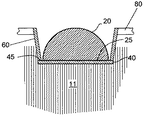
図6に、本発明の実施例による投影系PLの最終要素20を詳細に示す。図6に示す実施例では、パターン化されたビームを整形し、且つ/又は方向づける投影系PLの最後のレンズ要素である投影系の最終光学要素20が存在する。
FIG. 6 shows in detail the
ある実施例では、放射強度が、密になった状態に大きな影響を及ぼさない限り、193nmの放射を透過する材料は石英である。パターン化されたビームの放射強度は、最も小型になる傾向もある最終要素のところで最大になり、そのためこの要素は、それが石英からできている場合には、密になった状態の影響を受けると考えられる。したがって、ある実施例では、最終要素の材料は、代わりに、193nmにおいて密になった状態の影響を受けないことから、CaF2とすることができる。157nmの放射については、CaF2を使用することがさらに適用可能である。というのは、石英は、この波長の放射を透過しないからである。ただし、CaF2は、液浸リソグラフィ機器で使用する浸漬液11で溶解するか、或いは浸漬液11と反応することがある。 In one embodiment, the material that transmits 193 nm radiation is quartz unless the radiation intensity has a significant effect on the dense state. The radiation intensity of the patterned beam is highest at the final element, which tends to be the smallest, so this element is affected by the dense state if it is made of quartz it is conceivable that. Thus, in some embodiments, the material of the final element can instead be CaF 2 because it is not affected by the dense state at 193 nm. The 157nm emission, it is further applicable to use CaF 2. This is because quartz does not transmit radiation of this wavelength. However, CaF 2 may dissolve in the immersion liquid 11 used in immersion lithography equipment or may react with the immersion liquid 11.
投影系の最終要素20を保護するいくつかのやり方が、欧州特許出願第03257400.6号に開示されている。この出願全体をここに参照により組み込む。
Several ways of protecting the
投影系PLの最終要素にCaF2を使用することの別の懸念は、CaF2の熱膨張係数が極めて高いため(石英ガラス(fused silica)の熱膨張係数の40倍)、組み込む材料が異なる場合に大きな熱応力及び熱変形を誘起することなく投影系に組み込むことが難しい場合があることである。第1に、これらの応力及び変形は、膨張係数の差に比例して変化する。そのため、CaF2の光学要素を組み込むと、特に、最終レンズ要素の位置決め要件が、非液浸リソグラフィ機器の位置決め要件よりも2〜10倍厳しいことがある液浸リソグラフィ機器で問題になることがある。 Another concern with the use of CaF 2 as the final element of the projection system PL is that CaF 2 has a very high coefficient of thermal expansion (40 times the coefficient of thermal expansion of fused silica), so that different materials are incorporated. In some cases, it is difficult to incorporate it into a projection system without inducing large thermal stress and thermal deformation. First, these stresses and deformations change in proportion to the difference in expansion coefficients. Thus, incorporating CaF 2 optical elements can be problematic, especially in immersion lithography equipment where the positioning requirements of the final lens element can be 2-10 times more stringent than those of non-immersion lithography equipment. .
図6を参照すると、本発明の実施例による投影系の最終要素が示されている。基板に最も近い投影系の最終要素(例えば、レンズ)20の底面25は、最終要素20に設けられる石英ガラス層40によって保護される。この層の厚さは、50μm〜5mmの範囲とすることができ、最終要素20に接触結合又は接着結合させることができる。接触結合では、接着剤を使用せず、結合表面は、合わせて直接結合させるのに十分に滑らか且つ清浄にする。最終要素に結合させた後で、石英ガラス層40を所望の厚さに研削・研磨し、それによって石英ガラスの極めて薄い層を取り扱う際の固有の難点をなくすことができる。このように、ある実施例では、層40と最終要素20を合わせて結合し、単に最終要素20を被覆しない。
Referring to FIG. 6, the final element of the projection system according to an embodiment of the present invention is shown. The
この形態の結合により、CaF2と石英ガラスなどの異なる材料を結合させる場合にひときわ強い結合が得られるが、温度変化及び熱勾配により、結合に「吸込み(breathe)作用」が生じ、これら2種類の材料の熱膨張又は熱収縮の差により、応力が緩和するまで、これらの材料が離れることがある。熱分離の場合には通常、極めて迅速に結合が再構成されるが、最終要素が液体と接触しているときに、例えば、層40の研磨又は研削中に、或いは、液浸リソグラフィ機器の使用中にこれが起こると、液体が隙間に吸い込まれることがある。
This form of bonding provides a particularly strong bond when bonding different materials such as CaF 2 and quartz glass, but due to temperature changes and thermal gradients, a “breathing action” occurs in the bond, and these two types Due to differences in thermal expansion or contraction of these materials, these materials may leave until the stress is relieved. In the case of thermal separation, the bond is usually reconfigured very quickly, but when the final element is in contact with the liquid, for example during polishing or grinding of the
最終要素20と層40の間の結合を保護するために、層40と同じ材料の縁部障壁60が、基板から離れるように(投影系PLの残りの部分に向かって)層40から延び、それによって最終要素20が障壁で完全に取り囲まれ、そのため、最終要素20が液体11から遮蔽される。
To protect the bond between the
縁部障壁60は、層40の縁部の周りに取り付けられる。図に示すように、縁部障壁60は、最終要素20の底面25の縁部の先まで延びるプレート40の縁部に隣接して取り付けられる。例えば、プレート40の上部表面にではなく、層40の縁部の表面に縁部障壁60を結合することによって、他の構成が可能である。ある実施例では、縁部障壁60と層40の結合は融着である。PCT特許出願PCT/EP04/013310号は、このような結合技術を詳細に記載している。この出願全体をここに参照により組み込む。ある実施例では、縁部障壁60は、先端が切り取られた円錐の形態である。ただし、縁部障壁60は、最終要素20を収容し得る空洞が生成される限り、任意の形状とすることができる。
An
最終要素20は、おそらくは、ある実施例では、層40が最終要素20の底面から張り出すように最終要素20の底面と部分的に重なる面を有し、それによって、縁部障壁60を層40の上面に取り付けることができる。ある実施例では、縁部障壁60と最終要素20の間に隙間が残るが、このようにする必要はない。
The
図6に示すように、最終要素20は、縁部障壁60及び層40を介して投影系PSの本体の取付け部80に装着し得る。これは、温度及び取付けにより誘起される応力及び変形を大きく低減し得るので有利である。というのは、縁部障壁60が、取付け部80と最終要素20の間を切り離す働きをするからである。或いは、最終要素20は、層40を介して取付け部80に直接取り付けることができる。最終要素20の位置を測定するように構成された測定用のシステム又はセンサを、層40又は縁部障壁60に取り付けることもできる。投影系への取付け、又はセンサの取付けは、従来方式の手段によって実現可能である。
As shown in FIG. 6, the
石英ガラスを含む層40及び縁部障壁60によって本発明の実施例を説明してきたが、層40及び/又は縁部障壁60には、任意の適切な材料を使用し得る。ある実施例では、層40及び/又は縁部障壁60に使用する材料は、水以外の液体であり得る浸漬液におかされにくく、その熱膨張係数は、CaF2以外の材料であり得る最終要素20の材料の熱膨張係数よりも小さい。ある実施例では、この熱膨張係数は、最終要素の材料の熱膨張係数よりも少なくとも1/2、1/5、1/10、又は1/20である。最終要素20は、任意の適切な材料で作製することができる。
While embodiments of the present invention have been described with a
欧州特許出願第03257072.3号では、2ステージ、即ち複式ステージ型の液浸リソグラフィ機器の考え方が開示されている。このような機器は、基板を支持する2つのテーブルを備える。浸漬液がない第1位置のテーブルによって高さ出し測定を実施し、浸漬液が存在する第2位置のテーブルによって露光を実施する。或いは、この機器が備えるテーブルは1つだけである。 European Patent Application No. 03257072.3 discloses the idea of a two stage, ie, a dual stage immersion lithography apparatus. Such equipment comprises two tables that support the substrate. Height measurement is performed using a table at the first position where there is no immersion liquid, and exposure is performed using a table at the second position where the immersion liquid exists. Alternatively, this device has only one table.
本明細書では、ICの製作でリソグラフィ機器を使用することを具体的に参照することがあるが、本明細書で説明するリソグラフィ機器は、例えば、集積光学系、磁気ドメイン・メモリ用の誘導/検出パターン、フラット・パネル・ディスプレイ、液晶ディスプレイ(LCD)、薄膜磁気ヘッドなどの製作など、他の応用が可能であることを理解されたい。このような代替応用例の状況では、本明細書で用いる「ウエハ」又は「ダイ」という用語は、それぞれより一般の用語である「基板」又は「目標部分」と同義とみなし得ることが当業者には理解されよう。本明細書で言及する基板は、例えば、トラック(典型的には、基板にレジスト層を塗布し、露光されたレジストを現像するツール)、計測ツール、及び/又は検査ツール内で、露光前又は露光後に処理することがある。該当する場合には、上記その他の基板処理ツールに本明細書の開示を適用することができる。さらに、基板は、例えば多層ICを生成するために2回以上処理することがある。そのため、本明細書で用いる基板という用語は、複数の処理済み層をすでに含む基板を指すこともある。 Although specific reference may be made herein to the use of lithographic equipment in the manufacture of ICs, the lithographic equipment described herein may be used, for example, for integrated optics, inductive / magnetic domain memory It should be understood that other applications are possible, such as fabrication of detection patterns, flat panel displays, liquid crystal displays (LCDs), thin film magnetic heads, and the like. In the context of such alternative applications, those skilled in the art will appreciate that the terms “wafer” or “die” as used herein may be considered synonymous with the more general terms “substrate” or “target portion”, respectively. Will be understood. The substrate referred to herein may be, for example, a track (typically a tool that applies a resist layer to the substrate and develops the exposed resist), metrology tool, and / or inspection tool, before exposure or May be processed after exposure. Where applicable, the disclosure herein may be applied to the other substrate processing tools described above. Furthermore, the substrate may be processed more than once, for example to produce a multi-layer IC. As such, the term substrate as used herein may refer to a substrate that already contains multiple processed layers.
上記では、光リソグラフィの状況で本発明の実施例を利用することを具体的に参照したが、本発明は、例えばインプリント・リソグラフィなどの他の応用例で利用することができ、状況次第では、光リソグラフィに限定されないことを理解されたい。インプリント・リソグラフィでは、パターン化装置のトポグラフィが、基板に生成されるパターンを画定する。パターン化装置のトポグラフィは、基板に供給されたレジスト層に押し付けることができ、その後、電磁放射、熱、圧力、又はこれらの組合せを適用することによってレジストを硬化させる。パターン化装置をレジストから取り外し、それによって、レジストが硬化した後でレジスト中にパターンが残る。 While the above specifically refers to the use of embodiments of the present invention in the context of photolithography, the present invention can be used in other applications, such as imprint lithography, depending on the situation. It should be understood that the invention is not limited to optical lithography. In imprint lithography, the topography of the patterning device defines the pattern that is generated on the substrate. The topography of the patterning device can be pressed against the resist layer supplied to the substrate, and then the resist is cured by applying electromagnetic radiation, heat, pressure, or a combination thereof. The patterning device is removed from the resist, thereby leaving a pattern in the resist after the resist is cured.
本明細書で用いる「放射」及び「ビーム」という用語は、(例えば、約365、248、193、157、又は126nmの波長を有する)紫外(UV)放射、及び(例えば、5〜20nmの範囲の波長を有する)極紫外(EUV)放射、並びにイオン・ビーム又は電子ビームなどの粒子ビームを含めて、あらゆるタイプの電磁放射を包含する。 As used herein, the terms “radiation” and “beam” refer to ultraviolet (UV) radiation (eg, having a wavelength of about 365, 248, 193, 157, or 126 nm), and (eg, in the range of 5-20 nm). All types of electromagnetic radiation are included, including extreme ultraviolet (EUV) radiation (having a wavelength of) and particle beams such as ion beams or electron beams.
「レンズ」という用語は、状況次第では、屈折型、反射型、磁気型、電磁気型、及び静電気型の光学コンポーネントを含めて、様々なタイプの光学コンポーネントのいずれか1つ又はこれらの組合せを指すことがある。 The term “lens”, depending on the context, refers to any one or combination of various types of optical components, including refractive, reflective, magnetic, electromagnetic, and electrostatic optical components. Sometimes.
以上、本発明の特定の実施例を説明してきたが、上記で説明した以外の形でも本発明を実施し得ることを理解されたい。例えば、本発明は、上記で開示した方法を記述する機械可読命令からなる1つ又は複数のシーケンスを含むコンピュータ・プログラム、或いは、このようなコンピュータ・プログラムを記憶したデータ記憶媒体(例えば、半導体メモリ、磁気ディスク、又は光ディスク)の形態をとり得る。 While specific embodiments of the invention have been described above, it will be appreciated that the invention may be practiced otherwise than as described. For example, the present invention provides a computer program that includes one or more sequences of machine-readable instructions that describe the methods disclosed above, or a data storage medium (eg, a semiconductor memory) that stores such a computer program. , Magnetic disk, or optical disk).
浸漬液が浴の形態で提供されるか、基板の局所的な表面区域にのみ提供されるかに関わらず、本発明の1つ又は複数の実施例を、上記で述べたタイプなどの任意の液浸リソグラフィ機器に適用することができる。液体供給システムは、投影系と、基板及び/又は基板テーブルとの間のスペースに液体を提供する任意の機構である。液体供給システムは、1つ又は複数の構造、1つ又は複数の液体注入口、1つ又は複数のガス注入口、1つ又は複数のガス排出口、及び/又は1つ又は複数の液体排出口の任意の組合せを含み得る。この組合せにより、このスペースに液体が提供され、閉じ込められる。ある実施例では、このスペースの表面は、基板及び/又は基板テーブルの一部に限定することもできるし、このスペースの表面は、基板及び/又は基板テーブルの表面を完全に覆うこともできる。或いは、このスペースは、基板及び/又は基板テーブルを囲うこともできる。 Regardless of whether the immersion liquid is provided in the form of a bath or only on a localized surface area of the substrate, one or more embodiments of the present invention may be applied to any of the types described above. It can be applied to immersion lithography equipment. A liquid supply system is any mechanism that provides liquid to the space between the projection system and the substrate and / or substrate table. The liquid supply system may include one or more structures, one or more liquid inlets, one or more gas inlets, one or more gas outlets, and / or one or more liquid outlets. May be included in any combination. This combination provides and confines liquid in this space. In certain embodiments, the surface of the space can be limited to a portion of the substrate and / or substrate table, or the surface of the space can completely cover the surface of the substrate and / or substrate table. Alternatively, this space can enclose the substrate and / or the substrate table.
上記の説明は、例示するためのものであり、限定するためのものではない。そのため、添付の特許請求の範囲の範囲から逸脱することなく、上記で説明した本発明に改変を加えることができることが当業者には明らかであろう。 The above description is intended to be illustrative and not limiting. Thus, it will be apparent to one skilled in the art that modifications may be made to the invention described above without departing from the scope of the claims set out below.
10 液だめ
11 浸漬液
12 液体閉込め構造
14 排出口
15 注入口
16 ガス・シール
20 投影系の最終要素
25 最終要素の底面
40 石英ガラス層、プレート
60 縁部障壁
80 取付け部
AD 調節装置
B 放射ビーム
BD ビーム送達系
C 目標部分
CO コンデンサ
IF 位置センサ
IL 照明系、照明器
IN 統合器
MA マスク
MT 支持構造、マスク・テーブル
M1 マスク位置合わせマーク
M2 マスク位置合わせマーク
PM 第1位置決め装置
PL 投影系、投影レンズ
PS 投影系、レンズ系
PW 第2位置決め装置
P1 基板位置合わせマーク
P2 基板位置合わせーク
SO 放射源
W 基板、ウエハ
WT 基板テーブル、ウエハ・テーブル
DESCRIPTION OF
Claims (22)
前記投影系の最終要素と前記基板の間のスペースを液体で少なくとも部分的に充填するように構成された液体供給システムとを備え、
前記縁部障壁と前記最終要素との間に隙間を設けることを特徴とするリソグラフィ投影機器。 A projection system configured to project the patterned radiation beam onto a substrate, on the surface closest to the substrate, and the final element having a layer bonded to said surface, of the same material as the layer, A projection system including an edge barrier extending from the layer away from the substrate to shield the final element from liquid ;
A liquid supply system configured to at least partially fill a space between a final element of the projection system and the substrate with liquid ;
A lithographic projection apparatus , wherein a gap is provided between the edge barrier and the final element .
前記投影系の前記最終要素と前記基板の間のスペースを液体で少なくとも部分的に充填するように構成された液体供給システムと、
前記層と同じ材料の、前記液体から前記最終要素を遮蔽するために前記基板から離れるように前記層から延びる縁部障壁とを備え、
前記縁部障壁と前記最終要素との間に隙間を設けることを特徴とするリソグラフィ投影機器。 A projection system configured to project the patterned radiation beam onto a substrate, comprising a final element having a layer on the surface closest to the substrate, wherein the final element, Ri taken through the layer The attached projection system,
A liquid supply system configured to at least partially fill a space between the final element of the projection system and the substrate with liquid ;
An edge barrier of the same material as the layer and extending from the layer away from the substrate to shield the final element from the liquid;
A lithographic projection apparatus , wherein a gap is provided between the edge barrier and the final element .
前記基板に最も近い前記最終要素の表面には層が結合され、前記層と同じ材料の縁部障壁は、前記液体から前記最終要素を遮蔽するために、前記基板から離れるように前記層から延びており、
前記縁部障壁と前記最終要素との間に隙間を設けることを特徴とする方法。 Projecting a patterned beam of radiation onto a substrate via a liquid provided in a space between a final element of the projection system and the substrate, comprising:
The layers are bonded on the surface closest the final element in the substrate, the edge barrier of the same material as the layer, in order to shield the final element from the liquid, extending from the layer away from the substrate And
Providing a gap between the edge barrier and the final element .
前記層と同じ材料の、前記液体から前記最終要素を遮蔽するために前記基板から離れるように前記層から延びる縁部障壁を有し、
前記縁部障壁と前記最終要素との間に隙間を設けることを特徴とする方法。 Projecting a patterned radiation beam onto the substrate through a liquid provided in a space between the final element of the projection system and the substrate, the final element comprising the substrate Having a layer on the surface closest to, and through which the final element is supported ,
An edge barrier of the same material as the layer and extending from the layer away from the substrate to shield the final element from the liquid;
Providing a gap between the edge barrier and the final element .
Applications Claiming Priority (1)
| Application Number | Priority Date | Filing Date | Title |
|---|---|---|---|
| US11/022,939 US7405805B2 (en) | 2004-12-28 | 2004-12-28 | Lithographic apparatus and device manufacturing method |
Publications (2)
| Publication Number | Publication Date |
|---|---|
| JP2006191066A JP2006191066A (en) | 2006-07-20 |
| JP4383408B2 true JP4383408B2 (en) | 2009-12-16 |
Family
ID=35735374
Family Applications (1)
| Application Number | Title | Priority Date | Filing Date |
|---|---|---|---|
| JP2005375770A Expired - Fee Related JP4383408B2 (en) | 2004-12-28 | 2005-12-27 | Lithographic apparatus and device fabrication method |
Country Status (8)
| Country | Link |
|---|---|
| US (3) | US7405805B2 (en) |
| EP (1) | EP1677153B1 (en) |
| JP (1) | JP4383408B2 (en) |
| KR (1) | KR100742766B1 (en) |
| CN (1) | CN100510968C (en) |
| DE (1) | DE602005014731D1 (en) |
| SG (2) | SG144153A1 (en) |
| TW (1) | TWI329790B (en) |
Families Citing this family (11)
| Publication number | Priority date | Publication date | Assignee | Title |
|---|---|---|---|---|
| JP4843503B2 (en) | 2004-01-20 | 2011-12-21 | カール・ツァイス・エスエムティー・ゲーエムベーハー | Microlithographic projection exposure apparatus and measuring apparatus for projection lens |
| US7405805B2 (en) * | 2004-12-28 | 2008-07-29 | Asml Netherlands B.V. | Lithographic apparatus and device manufacturing method |
| US7450217B2 (en) | 2005-01-12 | 2008-11-11 | Asml Netherlands B.V. | Exposure apparatus, coatings for exposure apparatus, lithographic apparatus, device manufacturing method, and device manufactured thereby |
| DE102005024163A1 (en) * | 2005-05-23 | 2006-11-30 | Carl Zeiss Smt Ag | Optical system e.g. projection objective, for microlithography projection exposure system, has module insertable and removable as unit into system, and concave curved optical surface for capping cavity during operation of exposure system |
| GB2431670A (en) * | 2005-10-25 | 2007-05-02 | Zeiss Carl Smt Ag | Protective coating with windows for protection of optical element that is soluble in immersion liquid. |
| JP4514225B2 (en) * | 2005-11-16 | 2010-07-28 | キヤノン株式会社 | Exposure apparatus and device manufacturing method |
| DE102006021797A1 (en) * | 2006-05-09 | 2007-11-15 | Carl Zeiss Smt Ag | Optical imaging device with thermal damping |
| NL2003363A (en) * | 2008-09-10 | 2010-03-15 | Asml Netherlands Bv | Lithographic apparatus, method of manufacturing an article for a lithographic apparatus and device manufacturing method. |
| NL2003392A (en) * | 2008-09-17 | 2010-03-18 | Asml Netherlands Bv | Lithographic apparatus and a method of operating the apparatus. |
| NL2004497A (en) * | 2009-05-01 | 2010-11-02 | Asml Netherlands Bv | Lithographic apparatus and a method of operating the apparatus. |
| CN106474858A (en) * | 2015-08-26 | 2017-03-08 | 盐城市瓯华化学工业有限公司 | Gas-liquid cycle separator for chemical material production |
Family Cites Families (117)
| Publication number | Priority date | Publication date | Assignee | Title |
|---|---|---|---|---|
| DE221563C (en) | ||||
| DE206607C (en) | ||||
| DE242880C (en) | ||||
| DE224448C (en) | ||||
| GB1242527A (en) | 1967-10-20 | 1971-08-11 | Kodak Ltd | Optical instruments |
| US3573975A (en) | 1968-07-10 | 1971-04-06 | Ibm | Photochemical fabrication process |
| ATE1462T1 (en) | 1979-07-27 | 1982-08-15 | Werner W. Dr. Tabarelli | OPTICAL LITHOGRAPHY PROCESS AND DEVICE FOR COPYING A PATTERN ONTO A SEMICONDUCTOR DISC. |
| FR2474708B1 (en) | 1980-01-24 | 1987-02-20 | Dme | HIGH-RESOLUTION MICROPHOTOLITHOGRAPHY PROCESS |
| JPS5754317A (en) | 1980-09-19 | 1982-03-31 | Hitachi Ltd | Method and device for forming pattern |
| US4346164A (en) | 1980-10-06 | 1982-08-24 | Werner Tabarelli | Photolithographic method for the manufacture of integrated circuits |
| US4509852A (en) | 1980-10-06 | 1985-04-09 | Werner Tabarelli | Apparatus for the photolithographic manufacture of integrated circuit elements |
| US4390273A (en) | 1981-02-17 | 1983-06-28 | Censor Patent-Und Versuchsanstalt | Projection mask as well as a method and apparatus for the embedding thereof and projection printing system |
| JPS57153433A (en) | 1981-03-18 | 1982-09-22 | Hitachi Ltd | Manufacturing device for semiconductor |
| JPS58202448A (en) | 1982-05-21 | 1983-11-25 | Hitachi Ltd | Exposing device |
| DD206607A1 (en) | 1982-06-16 | 1984-02-01 | Mikroelektronik Zt Forsch Tech | METHOD AND DEVICE FOR ELIMINATING INTERFERENCE EFFECTS |
| DD242880A1 (en) | 1983-01-31 | 1987-02-11 | Kuch Karl Heinz | DEVICE FOR PHOTOLITHOGRAPHIC STRUCTURAL TRANSMISSION |
| DD221563A1 (en) | 1983-09-14 | 1985-04-24 | Mikroelektronik Zt Forsch Tech | IMMERSIONS OBJECTIVE FOR THE STEP-BY-STEP PROJECTION IMAGING OF A MASK STRUCTURE |
| DD224448A1 (en) | 1984-03-01 | 1985-07-03 | Zeiss Jena Veb Carl | DEVICE FOR PHOTOLITHOGRAPHIC STRUCTURAL TRANSMISSION |
| JPS6265326A (en) | 1985-09-18 | 1987-03-24 | Hitachi Ltd | Exposure device |
| JPS62121417A (en) | 1985-11-22 | 1987-06-02 | Hitachi Ltd | Liquid-immersion objective lens device |
| JPS63157419A (en) | 1986-12-22 | 1988-06-30 | Toshiba Corp | Fine pattern transfer apparatus |
| US5040020A (en) | 1988-03-31 | 1991-08-13 | Cornell Research Foundation, Inc. | Self-aligned, high resolution resonant dielectric lithography |
| JPH03209479A (en) | 1989-09-06 | 1991-09-12 | Sanee Giken Kk | Exposure method |
| US5121256A (en) | 1991-03-14 | 1992-06-09 | The Board Of Trustees Of The Leland Stanford Junior University | Lithography system employing a solid immersion lens |
| JPH04305915A (en) | 1991-04-02 | 1992-10-28 | Nikon Corp | Adhesion type exposure device |
| JPH04305917A (en) | 1991-04-02 | 1992-10-28 | Nikon Corp | Adhesion type exposure device |
| JPH06124873A (en) | 1992-10-09 | 1994-05-06 | Canon Inc | Liquid-soaking type projection exposure apparatus |
| JP2753930B2 (en) | 1992-11-27 | 1998-05-20 | キヤノン株式会社 | Immersion type projection exposure equipment |
| JP2520833B2 (en) | 1992-12-21 | 1996-07-31 | 東京エレクトロン株式会社 | Immersion type liquid treatment device |
| JPH07220990A (en) | 1994-01-28 | 1995-08-18 | Hitachi Ltd | Pattern forming method and exposure apparatus therefor |
| WO1998009278A1 (en) | 1996-08-26 | 1998-03-05 | Digital Papyrus Technologies | Method and apparatus for coupling an optical lens to a disk through a coupling medium having a relatively high index of refraction |
| US5825043A (en) | 1996-10-07 | 1998-10-20 | Nikon Precision Inc. | Focusing and tilting adjustment system for lithography aligner, manufacturing apparatus or inspection apparatus |
| JP3612920B2 (en) | 1997-02-14 | 2005-01-26 | ソニー株式会社 | Exposure apparatus for producing an optical recording medium master |
| JPH10255319A (en) | 1997-03-12 | 1998-09-25 | Hitachi Maxell Ltd | Master disk exposure device and method therefor |
| JP3747566B2 (en) | 1997-04-23 | 2006-02-22 | 株式会社ニコン | Immersion exposure equipment |
| JP3817836B2 (en) | 1997-06-10 | 2006-09-06 | 株式会社ニコン | EXPOSURE APPARATUS, ITS MANUFACTURING METHOD, EXPOSURE METHOD, AND DEVICE MANUFACTURING METHOD |
| US5900354A (en) | 1997-07-03 | 1999-05-04 | Batchelder; John Samuel | Method for optical inspection and lithography |
| JPH11176727A (en) | 1997-12-11 | 1999-07-02 | Nikon Corp | Projection aligner |
| EP1039511A4 (en) | 1997-12-12 | 2005-03-02 | Nikon Corp | Projection exposure method and projection aligner |
| AU2747999A (en) | 1998-03-26 | 1999-10-18 | Nikon Corporation | Projection exposure method and system |
| JP2000058436A (en) | 1998-08-11 | 2000-02-25 | Nikon Corp | Projection aligner and exposure method |
| TWI242111B (en) | 1999-04-19 | 2005-10-21 | Asml Netherlands Bv | Gas bearings for use in vacuum chambers and their application in lithographic projection apparatus |
| JP4504479B2 (en) | 1999-09-21 | 2010-07-14 | オリンパス株式会社 | Immersion objective lens for microscope |
| TW591653B (en) | 2000-08-08 | 2004-06-11 | Koninkl Philips Electronics Nv | Method of manufacturing an optically scannable information carrier |
| JP2002072090A (en) * | 2000-08-31 | 2002-03-12 | Olympus Optical Co Ltd | Wide-angle zoom lens |
| US20020163629A1 (en) | 2001-05-07 | 2002-11-07 | Michael Switkes | Methods and apparatus employing an index matching medium |
| US6600547B2 (en) | 2001-09-24 | 2003-07-29 | Nikon Corporation | Sliding seal |
| US6897941B2 (en) | 2001-11-07 | 2005-05-24 | Applied Materials, Inc. | Optical spot grid array printer |
| US7092069B2 (en) | 2002-03-08 | 2006-08-15 | Carl Zeiss Smt Ag | Projection exposure method and projection exposure system |
| DE10229818A1 (en) | 2002-06-28 | 2004-01-15 | Carl Zeiss Smt Ag | Focus detection method and imaging system with focus detection system |
| US6788477B2 (en) | 2002-10-22 | 2004-09-07 | Taiwan Semiconductor Manufacturing Co., Ltd. | Apparatus for method for immersion lithography |
| CN101382738B (en) | 2002-11-12 | 2011-01-12 | Asml荷兰有限公司 | Lithographic projection apparatus |
| JP3977324B2 (en) | 2002-11-12 | 2007-09-19 | エーエスエムエル ネザーランズ ビー.ブイ. | Lithographic apparatus |
| KR100588124B1 (en) | 2002-11-12 | 2006-06-09 | 에이에스엠엘 네델란즈 비.브이. | Lithographic Apparatus and Device Manufacturing Method |
| DE60335595D1 (en) | 2002-11-12 | 2011-02-17 | Asml Netherlands Bv | Immersion lithographic apparatus and method of making a device |
| SG121822A1 (en) | 2002-11-12 | 2006-05-26 | Asml Netherlands Bv | Lithographic apparatus and device manufacturing method |
| SG131766A1 (en) | 2002-11-18 | 2007-05-28 | Asml Netherlands Bv | Lithographic apparatus and device manufacturing method |
| TWI243288B (en) | 2002-11-26 | 2005-11-11 | Asml Netherlands Bv | Method of fabricating an optical element, lithographic apparatus and semiconductor device manufacturing method |
| KR101157002B1 (en) | 2002-12-10 | 2012-06-21 | 가부시키가이샤 니콘 | Exposure apparatus and method for manufacturing device |
| AU2003289272A1 (en) | 2002-12-10 | 2004-06-30 | Nikon Corporation | Surface position detection apparatus, exposure method, and device porducing method |
| CN1717776A (en) | 2002-12-10 | 2006-01-04 | 株式会社尼康 | Optical device and projection exposure apparatus using such optical device |
| KR20050085236A (en) | 2002-12-10 | 2005-08-29 | 가부시키가이샤 니콘 | Exposure apparatus and method for manufacturing device |
| AU2003289271A1 (en) | 2002-12-10 | 2004-06-30 | Nikon Corporation | Exposure apparatus, exposure method and method for manufacturing device |
| KR101085372B1 (en) | 2002-12-10 | 2011-11-21 | 가부시키가이샤 니콘 | Exposure apparatus and method for manufacturing device |
| DE10257766A1 (en) | 2002-12-10 | 2004-07-15 | Carl Zeiss Smt Ag | Method for setting a desired optical property of a projection lens and microlithographic projection exposure system |
| JP4232449B2 (en) | 2002-12-10 | 2009-03-04 | 株式会社ニコン | Exposure method, exposure apparatus, and device manufacturing method |
| EP1571697A4 (en) | 2002-12-10 | 2007-07-04 | Nikon Corp | Exposure system and device producing method |
| US7242455B2 (en) | 2002-12-10 | 2007-07-10 | Nikon Corporation | Exposure apparatus and method for producing device |
| JP4352874B2 (en) | 2002-12-10 | 2009-10-28 | 株式会社ニコン | Exposure apparatus and device manufacturing method |
| WO2004053953A1 (en) | 2002-12-10 | 2004-06-24 | Nikon Corporation | Exposure apparatus and method for manufacturing device |
| AU2003302831A1 (en) | 2002-12-10 | 2004-06-30 | Nikon Corporation | Exposure method, exposure apparatus and method for manufacturing device |
| WO2004055803A1 (en) | 2002-12-13 | 2004-07-01 | Koninklijke Philips Electronics N.V. | Liquid removal in a method and device for irradiating spots on a layer |
| JP4364805B2 (en) | 2002-12-19 | 2009-11-18 | コーニンクレッカ フィリップス エレクトロニクス エヌ ヴィ | Method and apparatus for irradiating a spot on a layer |
| EP1732075A3 (en) | 2002-12-19 | 2007-02-21 | Koninklijke Philips Electronics N.V. | Method and device for irradiating spots on a layer |
| KR101177331B1 (en) | 2003-04-09 | 2012-08-30 | 가부시키가이샤 니콘 | Immersion lithography fluid control system |
| EP2921905B1 (en) | 2003-04-10 | 2017-12-27 | Nikon Corporation | Run-off path to collect liquid for an immersion lithography apparatus |
| SG2012050829A (en) | 2003-04-10 | 2015-07-30 | Nippon Kogaku Kk | Environmental system including vacuum scavange for an immersion lithography apparatus |
| JP4650413B2 (en) | 2003-04-10 | 2011-03-16 | 株式会社ニコン | Environmental system including a transfer area for an immersion lithography apparatus |
| JP4656057B2 (en) | 2003-04-10 | 2011-03-23 | 株式会社ニコン | Electro-osmotic element for immersion lithography equipment |
| WO2004092830A2 (en) | 2003-04-11 | 2004-10-28 | Nikon Corporation | Liquid jet and recovery system for immersion lithography |
| KR101225884B1 (en) | 2003-04-11 | 2013-01-28 | 가부시키가이샤 니콘 | Apparatus and method for maintaining immersion fluid in the gap under the projection lens during wafer exchange in an immersion lithography machine |
| SG185136A1 (en) | 2003-04-11 | 2012-11-29 | Nikon Corp | Cleanup method for optics in immersion lithography |
| WO2004095135A2 (en) | 2003-04-17 | 2004-11-04 | Nikon Corporation | Optical arrangement of autofocus elements for use with immersion lithography |
| TWI295414B (en) | 2003-05-13 | 2008-04-01 | Asml Netherlands Bv | Lithographic apparatus and device manufacturing method |
| US7274472B2 (en) | 2003-05-28 | 2007-09-25 | Timbre Technologies, Inc. | Resolution enhanced optical metrology |
| DE10324477A1 (en) * | 2003-05-30 | 2004-12-30 | Carl Zeiss Smt Ag | Microlithographic projection exposure system |
| EP2261741A3 (en) | 2003-06-11 | 2011-05-25 | ASML Netherlands B.V. | Lithographic apparatus and device manufacturing method |
| JP4343597B2 (en) | 2003-06-25 | 2009-10-14 | キヤノン株式会社 | Exposure apparatus and device manufacturing method |
| JP2005019616A (en) | 2003-06-25 | 2005-01-20 | Canon Inc | Immersion type exposure apparatus |
| JP3862678B2 (en) | 2003-06-27 | 2006-12-27 | キヤノン株式会社 | Exposure apparatus and device manufacturing method |
| EP1498778A1 (en) | 2003-06-27 | 2005-01-19 | ASML Netherlands B.V. | Lithographic apparatus and device manufacturing method |
| EP2853943B1 (en) | 2003-07-08 | 2016-11-16 | Nikon Corporation | Wafer table for immersion lithography |
| SG109000A1 (en) | 2003-07-16 | 2005-02-28 | Asml Netherlands Bv | Lithographic apparatus and device manufacturing method |
| US8149381B2 (en) * | 2003-08-26 | 2012-04-03 | Nikon Corporation | Optical element and exposure apparatus |
| US7070915B2 (en) | 2003-08-29 | 2006-07-04 | Tokyo Electron Limited | Method and system for drying a substrate |
| US6954256B2 (en) | 2003-08-29 | 2005-10-11 | Asml Netherlands B.V. | Gradient immersion lithography |
| KR20170070264A (en) | 2003-09-03 | 2017-06-21 | 가부시키가이샤 니콘 | Apparatus and method for providing fluid for immersion lithography |
| JP4378136B2 (en) | 2003-09-04 | 2009-12-02 | キヤノン株式会社 | Exposure apparatus and device manufacturing method |
| JP3870182B2 (en) | 2003-09-09 | 2007-01-17 | キヤノン株式会社 | Exposure apparatus and device manufacturing method |
| JP2005159322A (en) | 2003-10-31 | 2005-06-16 | Nikon Corp | Surface plate, stage apparatus, exposure device and exposing method |
| US7545481B2 (en) | 2003-11-24 | 2009-06-09 | Asml Netherlands B.V. | Lithographic apparatus and device manufacturing method |
| EP1695148B1 (en) * | 2003-11-24 | 2015-10-28 | Carl Zeiss SMT GmbH | Immersion objective |
| JP2005175016A (en) | 2003-12-08 | 2005-06-30 | Canon Inc | Substrate holding device, exposure device using the same, and method of manufacturing device |
| JP2005175034A (en) | 2003-12-09 | 2005-06-30 | Canon Inc | Aligner |
| JP2005189850A (en) * | 2003-12-15 | 2005-07-14 | Carl Zeiss Smt Ag | Refractive projection objective lens for immersion lithography |
| JP5102492B2 (en) | 2003-12-19 | 2012-12-19 | カール・ツァイス・エスエムティー・ゲーエムベーハー | Objective lens for microlithography projection with crystal elements |
| US7460206B2 (en) * | 2003-12-19 | 2008-12-02 | Carl Zeiss Smt Ag | Projection objective for immersion lithography |
| US7589818B2 (en) | 2003-12-23 | 2009-09-15 | Asml Netherlands B.V. | Lithographic apparatus, alignment apparatus, device manufacturing method, and a method of converting an apparatus |
| JP2005191381A (en) | 2003-12-26 | 2005-07-14 | Canon Inc | Exposure method and system thereof |
| JP2005191393A (en) | 2003-12-26 | 2005-07-14 | Canon Inc | Exposing method and equipment |
| JP4429023B2 (en) | 2004-01-07 | 2010-03-10 | キヤノン株式会社 | Exposure apparatus and device manufacturing method |
| JP4018647B2 (en) | 2004-02-09 | 2007-12-05 | キヤノン株式会社 | Projection exposure apparatus and device manufacturing method |
| JP2005286068A (en) | 2004-03-29 | 2005-10-13 | Canon Inc | Exposure device and method therefor |
| JP4510494B2 (en) | 2004-03-29 | 2010-07-21 | キヤノン株式会社 | Exposure equipment |
| US7180572B2 (en) * | 2004-06-23 | 2007-02-20 | Taiwan Semiconductor Manufacturing Company, Ltd. | Immersion optical projection system |
| JP2006165285A (en) | 2004-12-08 | 2006-06-22 | Nikon Corp | Optical element and aligner |
| US7405805B2 (en) * | 2004-12-28 | 2008-07-29 | Asml Netherlands B.V. | Lithographic apparatus and device manufacturing method |
-
2004
- 2004-12-28 US US11/022,939 patent/US7405805B2/en not_active Expired - Fee Related
-
2005
- 2005-12-15 EP EP20050257739 patent/EP1677153B1/en not_active Expired - Fee Related
- 2005-12-15 DE DE200560014731 patent/DE602005014731D1/en active Active
- 2005-12-16 TW TW94144968A patent/TWI329790B/en not_active IP Right Cessation
- 2005-12-22 SG SG200804540-3A patent/SG144153A1/en unknown
- 2005-12-22 SG SG200508320A patent/SG123750A1/en unknown
- 2005-12-23 CN CN 200510003549 patent/CN100510968C/en not_active Expired - Fee Related
- 2005-12-27 JP JP2005375770A patent/JP4383408B2/en not_active Expired - Fee Related
- 2005-12-28 KR KR1020050132238A patent/KR100742766B1/en not_active IP Right Cessation
-
2008
- 2008-06-20 US US12/213,543 patent/US8013978B2/en not_active Expired - Fee Related
-
2011
- 2011-07-22 US US13/189,288 patent/US8913225B2/en not_active Expired - Fee Related
Also Published As
| Publication number | Publication date |
|---|---|
| KR100742766B1 (en) | 2007-07-25 |
| CN100510968C (en) | 2009-07-08 |
| SG144153A1 (en) | 2008-07-29 |
| KR20060076752A (en) | 2006-07-04 |
| US20080259296A1 (en) | 2008-10-23 |
| TW200629002A (en) | 2006-08-16 |
| SG123750A1 (en) | 2006-07-26 |
| DE602005014731D1 (en) | 2009-07-16 |
| EP1677153B1 (en) | 2009-06-03 |
| EP1677153A1 (en) | 2006-07-05 |
| JP2006191066A (en) | 2006-07-20 |
| US20060139589A1 (en) | 2006-06-29 |
| US8913225B2 (en) | 2014-12-16 |
| US20110279796A1 (en) | 2011-11-17 |
| US8013978B2 (en) | 2011-09-06 |
| US7405805B2 (en) | 2008-07-29 |
| CN1797208A (en) | 2006-07-05 |
| TWI329790B (en) | 2010-09-01 |
Similar Documents
| Publication | Publication Date | Title |
|---|---|---|
| JP4383408B2 (en) | Lithographic apparatus and device fabrication method | |
| JP5194050B2 (en) | Lithographic apparatus | |
| JP4473811B2 (en) | Lithographic apparatus and device manufacturing method | |
| JP4598133B2 (en) | Lithographic apparatus and device manufacturing method | |
| JP4146828B2 (en) | Lithographic apparatus and device manufacturing method | |
| JP5193349B2 (en) | Lithographic projection apparatus and device manufacturing method | |
| JP4728382B2 (en) | Lithographic apparatus and device manufacturing method | |
| JP4482531B2 (en) | Lithographic apparatus and device manufacturing method | |
| JP2008219017A (en) | Lithographic apparatus, alignment apparatus, device manufacturing method, aligning method, and method of converting apparatus | |
| JP4450782B2 (en) | Lithographic apparatus, device manufacturing method, and computer program product | |
| JP5412399B2 (en) | Lithographic apparatus and device manufacturing method | |
| JP5016705B2 (en) | Fluid handling structure |
Legal Events
| Date | Code | Title | Description |
|---|---|---|---|
| RD03 | Notification of appointment of power of attorney |
Free format text: JAPANESE INTERMEDIATE CODE: A7423 Effective date: 20060904 |
|
| RD05 | Notification of revocation of power of attorney |
Free format text: JAPANESE INTERMEDIATE CODE: A7425 Effective date: 20070529 |
|
| A977 | Report on retrieval |
Free format text: JAPANESE INTERMEDIATE CODE: A971007 Effective date: 20081106 |
|
| A131 | Notification of reasons for refusal |
Free format text: JAPANESE INTERMEDIATE CODE: A131 Effective date: 20081121 |
|
| A601 | Written request for extension of time |
Free format text: JAPANESE INTERMEDIATE CODE: A601 Effective date: 20090223 |
|
| A602 | Written permission of extension of time |
Free format text: JAPANESE INTERMEDIATE CODE: A602 Effective date: 20090226 |
|
| A521 | Written amendment |
Free format text: JAPANESE INTERMEDIATE CODE: A523 Effective date: 20090521 |
|
| TRDD | Decision of grant or rejection written | ||
| A01 | Written decision to grant a patent or to grant a registration (utility model) |
Free format text: JAPANESE INTERMEDIATE CODE: A01 Effective date: 20090915 |
|
| A01 | Written decision to grant a patent or to grant a registration (utility model) |
Free format text: JAPANESE INTERMEDIATE CODE: A01 |
|
| A61 | First payment of annual fees (during grant procedure) |
Free format text: JAPANESE INTERMEDIATE CODE: A61 Effective date: 20090918 |
|
| FPAY | Renewal fee payment (event date is renewal date of database) |
Free format text: PAYMENT UNTIL: 20121002 Year of fee payment: 3 |
|
| R150 | Certificate of patent or registration of utility model |
Ref document number: 4383408 Country of ref document: JP Free format text: JAPANESE INTERMEDIATE CODE: R150 Free format text: JAPANESE INTERMEDIATE CODE: R150 |
|
| S802 | Written request for registration of partial abandonment of right |
Free format text: JAPANESE INTERMEDIATE CODE: R311802 |
|
| FPAY | Renewal fee payment (event date is renewal date of database) |
Free format text: PAYMENT UNTIL: 20121002 Year of fee payment: 3 |
|
| R350 | Written notification of registration of transfer |
Free format text: JAPANESE INTERMEDIATE CODE: R350 |
|
| FPAY | Renewal fee payment (event date is renewal date of database) |
Free format text: PAYMENT UNTIL: 20131002 Year of fee payment: 4 |
|
| R250 | Receipt of annual fees |
Free format text: JAPANESE INTERMEDIATE CODE: R250 |
|
| R250 | Receipt of annual fees |
Free format text: JAPANESE INTERMEDIATE CODE: R250 |
|
| R250 | Receipt of annual fees |
Free format text: JAPANESE INTERMEDIATE CODE: R250 |
|
| R250 | Receipt of annual fees |
Free format text: JAPANESE INTERMEDIATE CODE: R250 |
|
| R250 | Receipt of annual fees |
Free format text: JAPANESE INTERMEDIATE CODE: R250 |
|
| R250 | Receipt of annual fees |
Free format text: JAPANESE INTERMEDIATE CODE: R250 |
|
| R250 | Receipt of annual fees |
Free format text: JAPANESE INTERMEDIATE CODE: R250 |
|
| LAPS | Cancellation because of no payment of annual fees |