JP4378136B2 - Exposure apparatus and device manufacturing method - Google Patents
Exposure apparatus and device manufacturing method Download PDFInfo
- Publication number
- JP4378136B2 JP4378136B2 JP2003312635A JP2003312635A JP4378136B2 JP 4378136 B2 JP4378136 B2 JP 4378136B2 JP 2003312635 A JP2003312635 A JP 2003312635A JP 2003312635 A JP2003312635 A JP 2003312635A JP 4378136 B2 JP4378136 B2 JP 4378136B2
- Authority
- JP
- Japan
- Prior art keywords
- liquid
- porous body
- substrate
- exposure apparatus
- optical element
- Prior art date
- Legal status (The legal status is an assumption and is not a legal conclusion. Google has not performed a legal analysis and makes no representation as to the accuracy of the status listed.)
- Expired - Lifetime
Links
Images


Classifications
-
- G—PHYSICS
- G03—PHOTOGRAPHY; CINEMATOGRAPHY; ANALOGOUS TECHNIQUES USING WAVES OTHER THAN OPTICAL WAVES; ELECTROGRAPHY; HOLOGRAPHY
- G03F—PHOTOMECHANICAL PRODUCTION OF TEXTURED OR PATTERNED SURFACES, e.g. FOR PRINTING, FOR PROCESSING OF SEMICONDUCTOR DEVICES; MATERIALS THEREFOR; ORIGINALS THEREFOR; APPARATUS SPECIALLY ADAPTED THEREFOR
- G03F7/00—Photomechanical, e.g. photolithographic, production of textured or patterned surfaces, e.g. printing surfaces; Materials therefor, e.g. comprising photoresists; Apparatus specially adapted therefor
- G03F7/70—Microphotolithographic exposure; Apparatus therefor
- G03F7/70216—Mask projection systems
- G03F7/70341—Details of immersion lithography aspects, e.g. exposure media or control of immersion liquid supply
Description
本発明は、例えば、半導体集積回路、撮像素子(CCD等)、液晶表示素子、又は薄膜磁気ヘッド等のデバイスを製造するためのリソグラフィー工程で用いられる投影露光装置に関し、特に投影光学系の基板側の素子と基板との間の光路中の少なくとも一部分に位置する液体を介して露光を行う液浸式露光装置に関するものである。 The present invention relates to a projection exposure apparatus used in a lithography process for manufacturing a device such as a semiconductor integrated circuit, an imaging device (CCD, etc.), a liquid crystal display device, or a thin film magnetic head, and more particularly to a substrate side of a projection optical system. The present invention relates to an immersion type exposure apparatus that performs exposure through a liquid located in at least a part of an optical path between the element and a substrate.
液浸式投影露光装置は被転写基板と、被転写基板に最も近い光学素子との間に液体を充填させることによって、NA(開口数)を上げることができるため、高解像度が期待されている。液浸式投影露光装置は被転写基板全体を液体の中に浸す方法や、被転写基板と被転写基板に最も近い光学素子との間だけに液体を充填させる方法などが提案されている(例えば、特許文献1及び特許文献2参照。)。 The liquid immersion type projection exposure apparatus can increase the NA (numerical aperture) by filling a liquid between the transfer target substrate and the optical element closest to the transfer target substrate, so that high resolution is expected. . For the immersion type projection exposure apparatus, a method of immersing the entire substrate to be transferred in a liquid, a method of filling the liquid only between the substrate to be transferred and the optical element closest to the substrate to be transferred, etc. have been proposed (for example, , See Patent Document 1 and Patent Document 2.)
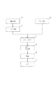
特に後者の方法では、International Symposium on 157nm Lithpgraphy,3−6 September2002,Belgiumにおいて、Bruce Smithら(Rochester Institute of Technology)によって講演されたExtreme−NA Water Immersion Lithography for35−65nm Technologyで、液浸式投影露光装置の液体供給方法および回収方法について示している。図7にその従来の技術の構成図を示す。図7において、101は基板、106は最終レンズ、107は液浸材となる液体、110は液体を供給する液体供給ノズル、111は液体を回収する液体回収ノズル、115は液体を外部に出さないために働くエアカーテンである。 In particular, in the latter method, International Symposium on 157 nm Lithogram, 3-6 September 2002, Belgium, by Bruce Smith et al. (Rochester Institute of Technology 35) It shows the liquid supply method and recovery method of the apparatus. FIG. 7 shows a configuration diagram of the prior art. In FIG. 7, 101 is a substrate, 106 is a final lens, 107 is a liquid that becomes an immersion material, 110 is a liquid supply nozzle that supplies the liquid, 111 is a liquid recovery nozzle that recovers the liquid, and 115 does not discharge the liquid to the outside. It is an air curtain that works for.
基板101と最終レンズ106との対向面に向けて、最終レンズ106のエッジ部近傍に搭載した液体供給ノズル110より液体107を供給する。そして、最終レンズ106を挟んで反対側に搭載した液体回収ノズル111から液体を回収する。さらに、それらの外側には圧縮空気をふきつけつことによってエアカーテンを形成し、基板101と最終レンズ106との間の液体を保持させる。 A liquid 107 is supplied from a liquid supply nozzle 110 mounted in the vicinity of the edge portion of the final lens 106 toward the opposing surface of the substrate 101 and the final lens 106. Then, the liquid is recovered from the liquid recovery nozzle 111 mounted on the opposite side across the final lens 106. In addition, an air curtain is formed by wiping compressed air on the outside thereof, and the liquid between the substrate 101 and the final lens 106 is held.
また、エアカーテンは示されていないものの、特許文献2においても液体供給ノズルと液体回収ノズルについて、図7と同様な構成で示されている。特許文献2ではさらに、基板101の移動速度に応じて、液体107の供給量と回収量の調整を行うことを示している。
しかしながら、上記従来例では以下のような課題があった。 However, the above conventional example has the following problems.
図7に示した構成では圧縮空気によるエアカーテンの調整が困難で、液体内部に空気が混入しやすい。さらに、基板ステージのステップ駆動あるいはスキャン駆動に伴う液体の流れによって、液体と外部の雰囲気との境界部に発生したメニスカスが破壊されやすくなるが、液体の境界部に発生したメニスカスが最終レンズ106の近傍にあるため、より基板101と最終光学レンズ106との間の液体に気泡が混入しやすくなる。気泡が液体内部に混入すると、露光光の妨げとなり、露光転写精度が低下し、半導体デバイス製造における歩留まりの低下を引き起こす。さらに、エアカーテンによる液体の圧力の保持が困難なので、液体の圧力が変動するに伴い、液体の密度が変動するため、屈折率が変動しやすくなり光学系のNA(開口数)が変化する。そのため露光転写精度の低下、すなわち半導体デバイス製造における歩留まりの低下を引き起こす。また、エアカーテンの空気の流れに混ざって液体が外部に飛び出す可能性があり、その液体によって露光装置内の部品などが損傷する可能性がある。そうすると、露光装置の修理や調整などにより露光装置の運転を止めなければならず、半導体デバイス製造における生産性が低下する。 In the configuration shown in FIG. 7, it is difficult to adjust the air curtain with compressed air, and air easily enters the liquid. Further, the meniscus generated at the boundary between the liquid and the external atmosphere is easily destroyed by the flow of the liquid accompanying step driving or scanning driving of the substrate stage, but the meniscus generated at the boundary of the liquid is Since it is in the vicinity, bubbles are more likely to be mixed into the liquid between the substrate 101 and the final optical lens 106. When bubbles are mixed in the liquid, the exposure light is hindered, the exposure transfer accuracy is lowered, and the yield in semiconductor device manufacturing is reduced. Furthermore, since it is difficult to maintain the pressure of the liquid by the air curtain, the density of the liquid changes as the liquid pressure changes, so that the refractive index easily changes and the NA (numerical aperture) of the optical system changes. For this reason, the exposure transfer accuracy is lowered, that is, the yield in semiconductor device manufacturing is lowered. Further, there is a possibility that the liquid may jump out to the outside due to mixing with the air flow of the air curtain, and the liquid in the exposure apparatus may be damaged by the liquid. Then, the operation of the exposure apparatus must be stopped due to repair or adjustment of the exposure apparatus, and productivity in semiconductor device manufacturing is reduced.
また、特許文献2の構成では基板の移動速度に応じて、液体の供給量と回収量の調整を行うとしているが、基板の移動には加速や減速があるため、その速度に応じて液体の供給量と回収量の調整を高精度に行うことが困難である。この場合、液体の供給量と回収量の調整を高精度に行うことができなければ、液体の圧力の保持が困難なので、液体の圧力が変動するに伴い、液体の密度が変動するため、屈折率が変動しやすくなり光学系のNA(開口数)が変化する。そのため露光転写精度の低下、すなわち半導体デバイス製造における歩留まりの低下を引き起こす。 Further, in the configuration of Patent Document 2, the liquid supply amount and the recovery amount are adjusted according to the movement speed of the substrate. However, since the movement of the substrate includes acceleration and deceleration, the liquid is adjusted according to the speed. It is difficult to adjust the supply amount and the recovery amount with high accuracy. In this case, if the liquid supply amount and the recovery amount cannot be adjusted with high accuracy, it is difficult to maintain the liquid pressure, and the liquid density fluctuates as the liquid pressure fluctuates. The rate tends to fluctuate, and the NA (numerical aperture) of the optical system changes. For this reason, the exposure transfer accuracy is lowered, that is, the yield in semiconductor device manufacturing is lowered.
図7で示した構成、ならびに特許文献2の構成に共通する課題として、液体の供給と回収を行う位置が限られているため、ステップ駆動あるいはスキャン駆動の駆動方向の自由度が低下する。ステップ駆動あるいはスキャン駆動の駆動方向の自由度が低下すると、スループットが低下するため、半導体デバイス製造における生産性が低下する。 As a problem common to the configuration shown in FIG. 7 and the configuration of Patent Document 2, since the positions where liquid supply and recovery are performed are limited, the degree of freedom in the drive direction of step drive or scan drive is reduced. When the degree of freedom in the driving direction of step driving or scanning driving decreases, the throughput decreases, so that productivity in semiconductor device manufacturing decreases.
本発明は斯かる点に鑑み、被転写基板と、投影光学系の最も被転写基板に近い光学素子との間に充填される液体に気泡を混入させず、かつその液体の圧力変動の小さい、すなわち液体の屈折率の変動が小さく、高解像度を実現することのできる露光装置を提供することを例示的な目的とする。 In view of such points, the present invention does not mix bubbles in the liquid filled between the transferred substrate and the optical element closest to the transferred substrate of the projection optical system, and the pressure fluctuation of the liquid is small. That is, it is an exemplary object to provide an exposure apparatus that can realize high resolution with a small change in the refractive index of the liquid.
上記目的を達成するために、本発明の一側面としての露光装置は、レチクルのパターンを基板に投影する投影光学系を有し、該投影光学系の最も前記基板側にある光学素子と前記基板との間の液体を介して前記基板を露光する露光装置において、前記液体を多孔質体を介して供給する供給系と、前記液体を回収する回収系と、多孔質体を介して前記光学素子と前記基板との間の前記液体内の気泡を除去する排気系と、を有することを特徴とする。 In order to achieve the above object, an exposure apparatus according to one aspect of the present invention has a projection optical system that projects a pattern of a reticle onto a substrate, and the optical element located on the most substrate side of the projection optical system and the substrate In an exposure apparatus that exposes the substrate via a liquid between, a supply system that supplies the liquid via a porous body , a recovery system that collects the liquid, and the optical element via a porous body And an exhaust system for removing bubbles in the liquid between the substrate and the substrate .
また、本発明の別の一側面としての露光装置は、レチクルのパターンを基板に投影する投影光学系を有し、該投影光学系の最も前記基板側にある光学素子と前記基板との間の液体を介して前記基板を露光する露光装置において、前記液体を供給する供給系と、前記液体を多孔質体を介して回収する回収系と、多孔質体を介して前記光学素子と前記基板との間の前記液体内の気泡を除去する排気系と、を有することを特徴とする。
An exposure apparatus according to another aspect of the present invention includes a projection optical system that projects a pattern of a reticle onto a substrate, and the optical element that is closest to the substrate of the projection optical system is disposed between the substrate and the optical element. In an exposure apparatus that exposes the substrate via a liquid, a supply system that supplies the liquid, a recovery system that collects the liquid via a porous body, the optical element and the substrate via a porous body, And an exhaust system for removing bubbles in the liquid.
更に、本発明の別の一側面としての露光装置は、レチクルのパターンを基板に投影する投影光学系を有し、該投影光学系の最も前記基板側にある光学素子と前記基板との間の液体を介して前記基板を露光する露光装置において、多孔質体を介して前記液体を供給する供給系と、前記液体を回収する回収系と、を有することを特徴とする。 Further, the exposure apparatus as another aspect of the present invention includes a projection optical system for projecting a pattern of a reticle onto a substrate, between the substrate and the optical element in the most the substrate side of the projection optical system An exposure apparatus that exposes the substrate through a liquid includes a supply system that supplies the liquid through a porous body and a recovery system that collects the liquid.
更に、本発明の別の一側面としての露光装置は、レチクルのパターンを基板に投影する投影光学系を有し、該投影光学系の最も前記基板側にある光学素子と前記基板との間の液体を介して前記基板を露光する露光装置において、第一の多孔質体を介して前記液体を供給する供給系と、第二の多孔質体を介して前記液体を回収する回収系と、を有し、前記第一多孔質体の前記基板に対向する面と前記第二多孔質体の前記基板に対向する面とは、前記基板から同じ高さに保たれていることを特徴とする。 Furthermore, an exposure apparatus according to another aspect of the present invention has a projection optical system that projects a pattern of a reticle onto a substrate, and is provided between an optical element closest to the substrate of the projection optical system and the substrate. In an exposure apparatus that exposes the substrate through a liquid, a supply system that supplies the liquid through a first porous body, and a recovery system that recovers the liquid through a second porous body. The surface of the first porous body facing the substrate and the surface of the second porous body facing the substrate are maintained at the same height from the substrate. To do.
更に、本発明の別の一側面としてのデバイス製造方法は、上記の露光装置を用いて基板を露光する工程と、該露光した基板を現像する工程とを有することを特徴とする。 Furthermore, a device manufacturing method according to another aspect of the present invention includes a step of exposing a substrate using the above exposure apparatus and a step of developing the exposed substrate.
本発明の更なる目的又はその他の特徴は、添付図面を参照して説明される以下の好ましい実施の形態によって明らかにされるであろう。 Further objects and other features of the present invention will become apparent from the following preferred embodiments described with reference to the accompanying drawings.
性能の良い液浸式投影露光装置を提供することができる。 An immersion type projection exposure apparatus with good performance can be provided.
本発明の好ましい実施の形態の詳細について、添付の図面をもとに、以下説明する。 Details of a preferred embodiment of the present invention will be described below with reference to the accompanying drawings.
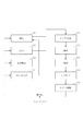
図1は本実施例を表す模式図である。 FIG. 1 is a schematic diagram showing this embodiment.
回路パターンなどを転写する被転写体としての基板1は基板保持部2で保持する。その保持方法は真空保持や静電保持などがある。そして、基板保持部2は基板ステージ3に搭載されており、基板ステージ3はステージ定盤4にならってステップ駆動、あるいはスキャン駆動し、ステップ駆動あるいはスキャン駆動時には不図示のAFセンサの計測結果に基づき、基板1が所定の高さになるよう基盤ステージ3で制御する。
A substrate 1 as a transfer target to which a circuit pattern or the like is transferred is held by a substrate holder 2. The holding method includes vacuum holding and electrostatic holding. The substrate holding unit 2 is mounted on a
一方、光学系は不図示の光源、その光源からの光で転写パターンが描かれたレチクルを照明する照明系と、および鏡筒5内に搭載した投影光学系、そして投影光学系の最も基板1よりの最終光学素子6からなる。そして、液浸式投影露光装置の特徴である液体7は基板1と最終光学素子6との間に充填されている。液体7は例えば水やフッ素化合物などがあり、基板1上に塗布されたレジストの種類や露光光の波長に応じて選定することができる。
On the other hand, the optical system is a light source (not shown), an illumination system for illuminating a reticle on which a transfer pattern is drawn with light from the light source, a projection optical system mounted in the lens barrel 5, and the most substrate 1 of the projection optical system. The final
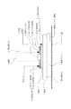
本実施例では最終光学素子6の周りに第一の多孔質体8と第二の多孔質体9を設ける。第一の多孔質体8は、例えばポリテトラフロロエチレン(PTFE)を延伸加工してできる微細な連続多孔質構造などからなり、気体は通すが液体7は通さない性質を持つ。第二の多孔質体9はスポンジなどのように、多孔質内部の毛細管現象で液体7を吸収する性質を持つ。そして、液体供給系10から第二の多孔質体9を介して基板1と最終光学素子6との間に液体7を供給する。なお、液体供給系10は液体供給源と液体供給管10a、ならびに液体供給管先端の液体供給ノズル10bからなる。液体供給ノズル10bは第二の多孔質体9と接続もしくは概ね接触している。第二の多孔質体9はその全体で液体7を吸収でき、吸収量が飽和したときに液体供給ができるため、基板1と対向している面の全体から液体7を供給することができる。このときの液体供給ノズル10bから第二の多孔質体9への液体7の供給量は、第二の多孔質体9の液体7を吸収する量が常に飽和した状態を保つように、不図示の第一の制御部で制御することが好ましい。また、基板ステージ3のステップ駆動あるいはスキャン駆動によって、基板1上に残った液体7は液体回収系11から回収する。なお、液体回収系11は液体回収ポンプと液体回収管11a、ならびに液体回収管先端の液体回収ノズル11bからなる。このときの液体回収量は第一の制御部で制御した液体供給量と同量にするように、不図示の第二の制御部で制御する。液体回収ノズル11bは第二の多孔質体9の外周に配置しているが、最終光学素子6の外周であればその位置は任意である。さらに、第一の多孔質体8と接続した真空排気系12から液体7内部の気泡のみ除去することによって、供給された液体7の中に混入した気泡が基板1と最終光学素子6との間に入る前に、その気泡を除去することができる。
In this embodiment, a first porous body 8 and a second porous body 9 are provided around the final
次に図2を用いて、多孔質体まわりの構成を説明する。図2は本実施例の第一の多孔質体8と第二の多孔質体9を表す断面図である。 Next, the configuration around the porous body will be described with reference to FIG. FIG. 2 is a cross-sectional view showing the first porous body 8 and the second porous body 9 of this embodiment.
図1では装置構成の説明を簡略化するため、最終光学素子6のまわりに直接第一の多孔質体8を配置し、さらに真空排気系12を第一の多孔質体8から直接接続した図を示した。しかしながら、この構成では第一の多孔質体8と真空排気系12との接触部の雰囲気だけが、真空排気系12から排気されてしまい、液体7に混入した気泡除去をするという第一の多孔質体8の本来の目的が果たせない。そのため、新たに多孔質体保持部13を設ける。多孔質体保持部13はその内側に最終光学素子6が搭載されるべきスペースを有し、外側には第二の多孔質体9が搭載できるようにする。多孔質体保持部14の内部は第一の多孔質体8が入っており、基板1との対向面(図2における下側の面)は開放され、第一の多孔質体8と直接対向できる構成となっている。なお、多孔質体保持部13の材質はステンレス鋼やアルミなど金属、あるいはガラスなどでも良い。図2では第一の多孔質体8上部と多孔質体保持部13との間に隙間を持たせたが、それ以外の接触面は隙間がないことが好ましい。さらに、第一の多孔質体8上部と多孔質体保持部13との間に隙間を設け、その隙間が真空排気のバッファの役割を果たすことを意味しているが、この隙間は必ずしも必要はない。なお、真空排気系12は液体7内に混入した気泡を排気する排気ポンプと該排気ポンプに接続した気泡排気管からなり、さらに気泡排気管と多孔質体保持部13とを接続する接続部がある。従って、多孔質体8上部と気泡排気管との間には、隙間がある。
In FIG. 1, in order to simplify the explanation of the apparatus configuration, a first porous body 8 is arranged directly around the final
図2では液体供給系10と液体回収系11、真空排気系12を一本ずつ図示したが、これに限定されず、それらの本数および配置は任意である。例えば、基板ステージ3のステップ駆動あるいはスキャン駆動は基板ステージ3の往復駆動を伴うため、液体供給系10や液体回収系11は双方向にある方が好ましい。
In FIG. 2, the liquid supply system 10, the liquid recovery system 11, and the
また、図1および図2では二種類の多孔質体を最終光学素子6側から、第一の多孔質体8、第二の多孔質体13の順番で配置したが、この順番は逆でも良いし、交互に複数層の配置にしても良い。例えば図3に示すように、最終光学素子6の外周に第一の多孔質体8と第二の多孔質体9をそれぞれ設ける。こうすることによって、液体7内部に混入した気泡は第一の多孔質体8越しに除去することができ、第二の多孔質体9全面から液体7を安定して供給することができる。つまり、液体を供給する際、できるだけ広範囲から液体を供給することによって、単位面積あたりの流量を減らすことができるのである。
In FIG. 1 and FIG. 2, two types of porous bodies are arranged in the order of the first porous body 8 and the second porous body 13 from the final
さらに、第一の多孔質体8は気体を通し液体7は通さない性質を持つものであれば、多孔質体に限らない。同様に第二の多孔質体9は液体7を吸収する性質を持つものであれば、多孔質体に限らない。 Further, the first porous body 8 is not limited to the porous body as long as it has a property of allowing gas to pass and not allowing the liquid 7 to pass. Similarly, the second porous body 9 is not limited to the porous body as long as it has a property of absorbing the liquid 7.
図1と図2では、第一の多孔質体8と第二の多孔質体9は最終光学素子6の基板1側の面と同じ高さに保たれているように示した。そして図3では、第二の多孔質体9が最終光学素子6の基板1側の面と同じ高さに保たれているように示した。基板1と最終光学素子6との間隙は数十μmからミリメートルオーダの距離である。したがって、第一の多孔質体8および/または第二の多孔質体9も最終光学素子6の基板1側の面と同じ高さに保たれていることが好ましいが、それに限定されない。基板1と第一の多孔質体8、第二の多孔質体9との間隙はそれぞれ任意である。
1 and 2, the first porous body 8 and the second porous body 9 are shown to be kept at the same height as the surface of the final
さらに、第一の多孔質体8あるいは多孔質体保持部13、第二の多孔質体9は最終光学素子6と同心円状の形状に示したが、これに限定されず、四角形など形状は任意である。また最終光学素子6の外周に対して全周に渡り第一の多孔質体8と第二の多孔質体9があることが好ましいが、それらは最終光学素子6の外周の少なくともステップ、スキャン方向の一部にあれば良い。第一の多孔質体8や第二の多孔質体9の大きさも、最終光学素子6に対する大きさが図示のような比率に限定されず、任意である。多孔質体保持部13は第一の多孔質体8のみを覆う構成を示したが、これに限定されず、第二の多孔質体9も含めた構成にしても良い。
Furthermore, the first porous body 8 or the porous body holding portion 13 and the second porous body 9 are shown in a concentric shape with the final
図4は本実施例の第一の多孔質体から第三の多孔質体を表す断面図である。 FIG. 4 is a cross-sectional view showing the first to third porous bodies in the present example.
第一の実施例では基板1に残留した液体7を液体回収系11から直接回収したが、第二の実施例では新たに第三の多孔質体14を設け、第三の多孔質体14から液体7を回収する。なお、第一の実施例で説明した構成や機能など、重複する部分の説明は省略する。
In the first embodiment, the liquid 7 remaining on the substrate 1 is directly recovered from the liquid recovery system 11. However, in the second embodiment, a third
第三の多孔質体14はスポンジなどのように、多孔質内部の毛細管現象で液体7を保持する性質を持ち、第二の多孔質体9と同じ種類の多孔質体でも良い。液体回収系11は第三の多孔質体14に接続もしくは概ね接触する。第三の多孔質体14は通常、液体7を吸収していない状態で、すなわち乾いた状態で使用し、基板1上に残った液体7を除去する。このときの液体回収量は第三の多孔質体14の液体7を吸収する量が飽和しないように、常に吸収力を維持するための不図示の第二の制御部で制御することが好ましい。なお、液体7を十分に吸収した第二の多孔質体9と、液体7を吸収していない第三の多孔質体14が隣接すると、第二の多孔質体9に吸収された液体7が第三の多孔質体14に直接吸収され、基板1上に残った液体7を除去するという第三の吸収体14の本来の機能が低下する。そのため、第二の多孔質体9と第三の多孔質体14との間には壁が必要であるが、図4では不図示とした。
The third
以上の説明では液体7の回収方法を第三の多孔質体14に吸収させてから、液体回収系11によって回収するとしたが、これに限定されない。例えば、液体回収系11がなくても、第三の多孔質体14が十分な量の液体7を吸収できれば、液体7を所定の量だけ吸収したときや、何枚かの基板1を露光してから、新しいものにあるいは乾いたものに交換しても良い。その場合は別途、第三の多孔質体14の交換手段が必要となる。
In the above description, the recovery method of the liquid 7 is absorbed by the third
第一の実施例でも説明した通り、基板1と最終光学素子6との間隙は数十μmからミリメートルオーダの距離である。第一の多孔質体8と第二の多孔質体9と同様に、第三の多孔質体14は最終光学素子6の基板1側の面と同じ高さに保たれていることが好ましいが、それに限定されず、基板1と第一の多孔質体8、第二の多孔質体9、第三の多孔質体14との間隙はそれぞれ任意である。さらに、第一の多孔質体8あるいは多孔質体保持部13、第二の多孔質体9と同様に、第三の多孔質体14も最終光学素子6と同心円状の形状に示したが、これに限定されず、四角形など形状は任意である。そして、最終光学素子6の外周に対して全周に渡り第一の多孔質体8と第二の多孔質体9、第三の多孔質体14があることが好ましいが、それらは最終光学素子6の外周の少なくともステップ、スキャン方向の一部にあれば良い。第一の多孔質体8や第二の多孔質体9、第三の多孔質体14の大きさも、最終光学素子6に対する大きさが図示のような比率に限定されず、任意である。多孔質体保持部13は第一の多孔質体8のみを覆う構成を示したが、これに限定されず、第二の多孔質体9や第三の多孔質体1も含めた構成にしても良い。
As described in the first embodiment, the gap between the substrate 1 and the final
また、第三の多孔質体は液体7を吸収する性質を持つものであれば、多孔質体に限らない。 The third porous body is not limited to the porous body as long as it has a property of absorbing the liquid 7.
図5は本実施例の第一の多孔質体を表す断面図である。 FIG. 5 is a cross-sectional view showing the first porous body of this example.
第一の実施例と第二の実施例では複数の多孔質体を使用することによって、液体の供給、回収および液体7内に混入した気泡を除去する構成について説明した。第三の実施の形態では多孔質体に第一の多孔質体8を使用し、その周りに取り付けたノズルから液体を供給、回収する。なお、第一の実施例と第二の実施例で説明した構成や機能など、重複する部分の説明は省略する。 In the first embodiment and the second embodiment, a configuration in which a plurality of porous bodies are used to supply and recover liquid and remove bubbles mixed in the liquid 7 has been described. In the third embodiment, the first porous body 8 is used as the porous body, and the liquid is supplied and recovered from a nozzle attached around the first porous body 8. In addition, description of the overlapping part, such as a structure and function demonstrated in the 1st Example and the 2nd Example, is abbreviate | omitted.
第一の多孔質体8は多孔質体保持部13の中に保持されており、多孔質体保持部13の外側は、真空排気系12が装備され、真空排気系12から液体7の中に混入した気泡を除去する構成となっている。また、多孔質体保持部13の外周には液体供給系10と液体回収系11が装備されており、液体供給系10から基板1と最終光学素子6との間に液体7を供給し、液体回収系11からその液体7を回収する構成となっている。なお、基板1に残った液体7を回収する構成は液体回収系11から直接回収するに限定されず、第二の実施例で説明したように、図5では不図示の第三の多孔質体14を多孔質体保持部13のまわりに取り付けても良い。
The first porous body 8 is held in the porous body holding portion 13, and the outside of the porous body holding portion 13 is equipped with a
図6は本実施例の第二の多孔質体を表す断面図である。 FIG. 6 is a cross-sectional view showing a second porous body of this example.
第一の実施例と第二の実施例では複数の多孔質体を使用することによって、液体の供給、回収および液体7内に混入した気泡を除去する構成について説明した。第四の実施の形態では多孔質体に第二の多孔質体9を使用し、その第二の多孔質体9から液体を供給し、その周りに取り付けたノズルから液体を回収する。なお、第一の実施例と第二の実施例で説明した構成や機能など、重複する部分の説明は省略する。 In the first embodiment and the second embodiment, a configuration in which a plurality of porous bodies are used to supply and recover liquid and remove bubbles mixed in the liquid 7 has been described. In the fourth embodiment, the second porous body 9 is used as the porous body, the liquid is supplied from the second porous body 9, and the liquid is recovered from the nozzle attached around the second porous body 9. In addition, description of the overlapping part, such as a structure and function demonstrated in the 1st Example and the 2nd Example, is abbreviate | omitted.
なお、基板1に残った液体7を回収する構成は液体回収系11から直接回収するに限定されず、第二の実施例で説明したように、図6では不図示の第三の多孔質体14を多孔質体保持部13のまわりに取り付けても良い。 The configuration for recovering the liquid 7 remaining on the substrate 1 is not limited to recovering directly from the liquid recovery system 11, but as described in the second embodiment, a third porous body (not shown in FIG. 6) is used. 14 may be attached around the porous body holding portion 13.
以上の実施例によれば、液浸式投影露光装置において、基板と最終光学素子との間の液体を保持することができるため、エアカーテンを使用する必要がなく、しいてはエアカーテンによって基板と最終光学素子との間の液体に気泡が混入することがなくなる。また、多孔質体を設けることにより液体と外部の雰囲気との境界に発生するメニスカスが、最終光学素子から遠ざかるため、メニスカスが破壊されても基板と最終光学素子との間の液体に気泡が混入することがなくなる。したがって、液体内部の気泡に起因する露光転写精度の低下を防止することができる。そして、エアカーテンを使わない液体の供給および/または回収方法は、多孔質体から必要に応じた流量しか与えないため、液体の圧力変動を抑制することができ、液体の密度が変動することがなくなるので、液体の屈折率の変動を抑えることができる。しいては光学系のNA(開口数)の変化を抑えることができる。したがって、光学系のNAの変化に起因する露光転写制度の低下を防止することができる。さらに、液体の供給と回収が露光領域を囲むような構成となっているため、ステップ駆動あるいはスキャン駆動の自由度が向上し、スループットが向上する。また、基板上に付着して残った液体を液浸式投影露光装置内に撒き散らすことなく回収できるので、液体を撒き散らすことによって起因する部品損傷を防止することができる。そのため、装置の運転を停止することを減らすことができる。以上の効果をまとめると、露光転写精度を向上し、スループットを向上させ、そして装置の運転の停止を抑制することができるため、半導体デバイス製造における生産性を向上させる液浸式投影露光装置を提供することができる。 According to the above embodiment, in the immersion type projection exposure apparatus, since the liquid between the substrate and the final optical element can be held, it is not necessary to use an air curtain, and the substrate is used by the air curtain. No bubbles are mixed into the liquid between the first optical element and the final optical element. In addition, since the meniscus generated at the boundary between the liquid and the external atmosphere moves away from the final optical element by providing a porous body, bubbles are mixed in the liquid between the substrate and the final optical element even if the meniscus is destroyed There is no longer to do. Therefore, it is possible to prevent a decrease in exposure transfer accuracy due to bubbles inside the liquid. The liquid supply and / or recovery method that does not use an air curtain provides only the required flow rate from the porous body, so that the liquid pressure fluctuation can be suppressed and the liquid density can fluctuate. Therefore, fluctuations in the refractive index of the liquid can be suppressed. As a result, changes in the NA (numerical aperture) of the optical system can be suppressed. Accordingly, it is possible to prevent the exposure transfer system from being lowered due to the change in the NA of the optical system. Further, since the liquid supply and recovery are configured to surround the exposure area, the degree of freedom of step driving or scanning driving is improved, and the throughput is improved. In addition, since the liquid remaining on the substrate can be recovered without being scattered in the immersion type projection exposure apparatus, it is possible to prevent component damage caused by scattering of the liquid. Therefore, it is possible to reduce stopping the operation of the apparatus. Summarizing the above effects, an immersion projection exposure apparatus that improves productivity in semiconductor device manufacturing is provided because exposure transfer accuracy can be improved, throughput can be improved, and stoppage of the operation of the apparatus can be suppressed. can do.
次に、前述した本発明の露光装置を利用したデバイスの製造方法の実施例を説明する。 Next, an embodiment of a device manufacturing method using the above-described exposure apparatus of the present invention will be described.
図8はデバイス(ICやLSI等の半導体チップ、液晶パネルやCCD)の製造フローを示す。ステップ1(回路設計)では半導体デバイスの回路設計を行う。ステップ2(マスク製作)では設計した回路パターンを形成したマスク(レチクル)を製作する。一方、ステップ3(ウエハ製造)ではシリコン等の材料を用いて基板としてのウエハを製造する。ステップ4(ウエハプロセス)は前工程と呼ばれ、上記用意したマスクとウエハとを用いて、リソグラフィー技術によってウエハ上に実際の回路を形成する。次のステップ5(組み立て)は後工程と呼ばれ、ステップ4よって作成されたウエハを用いてチップ化する工程であり、アッセンブリ工程(ダイシング、ボンディング)、パッケージング工程(チップ封入)等の工程を含む。ステップ6(検査)ではステップ5で作成された半導体デバイスの動作確認テスト、耐久性テスト等の検査を行う。こうした工程を経て半導体デバイスが完成し、これが出荷(ステップ7)される。 FIG. 8 shows a manufacturing flow of devices (semiconductor chips such as IC and LSI, liquid crystal panels and CCDs). In step 1 (circuit design), a semiconductor device circuit is designed. In step 2 (mask production), a mask (reticle) on which the designed circuit pattern is formed is produced. On the other hand, in step 3 (wafer manufacture), a wafer as a substrate is manufactured using a material such as silicon. Step 4 (wafer process) is called a pre-process, and an actual circuit is formed on the wafer by lithography using the prepared mask and wafer. The next step 5 (assembly) is called a post-process, and is a process for forming a chip using the wafer created in step 4, and the assembly process (dicing, bonding), packaging process (chip encapsulation) and the like are performed. Including. In step 6 (inspection), inspections such as an operation confirmation test and a durability test of the semiconductor device created in step 5 are performed. Through these steps, the semiconductor device is completed and shipped (step 7).
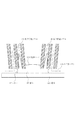
図9は上記ウエハプロセスの詳細なフローを示す。ステップ11(酸化)ではウエハの表面を酸化させる。ステップ12ではウエハの表面に絶縁膜を形成する。ステップ13(電極形成)ではウエハ上に電極を蒸着によって形成する。ステップ14(イオン打ち込み)ではウエハにイオンを打ち込む。ステップ15(レジスト処理)ではウエハにレジスト(感材)を塗布する。ステップ16(露光)では前述の本発明の露光装置によってマスクの回路パタ−ンの像でウエハを露光する。ステップ17(現像)では露光したウエハを現像する。ステップ18(エッチング)では現像したレジスト以外の部分を削り取る。ステップ19(レジスト剥離)ではエッチングが済んで不要となったレジストを取り除く。これらステップを繰り返し行うことによりウエハ上に回路パタ−ンが形成される。
FIG. 9 shows a detailed flow of the wafer process. In step 11 (oxidation), the wafer surface is oxidized. In
本実施例の製造方法を用いれば、従来は難しかった高集積度のデバイスを製造することが可能になる。 By using the manufacturing method of this embodiment, it becomes possible to manufacture a highly integrated device, which has been difficult in the past.
以上、本発明の好ましい実施の形態を説明したが、本発明はこれに限定されず、その要旨の範囲内で様々な変形や変更が可能である。 As mentioned above, although preferable embodiment of this invention was described, this invention is not limited to this, A various deformation | transformation and change are possible within the range of the summary.
1 基板
2 基板保持部
3 基板ステージ
4 ステージ定盤
5 鏡筒
6 最終光学素子
7 液体
8 第一の多孔質体
9 第二の多孔質体
10 液体供給系
10a 液体供給管
10b 液体供給ノズル
11 液体回収系
11a 液体回収管
11b 液体回収ノズル
12 真空排気系
13 多孔質体保持部
14 第三の多孔質体
DESCRIPTION OF SYMBOLS 1 Substrate 2
Claims (6)
前記液体を多孔質体を介して供給する供給系と、
前記液体を回収する回収系と、
多孔質体を介して前記光学素子と前記基板との間の前記液体内の気泡を除去する排気系と、を有することを特徴とする露光装置。 In an exposure apparatus that has a projection optical system that projects a pattern of a reticle onto a substrate, and that exposes the substrate through a liquid between an optical element closest to the substrate of the projection optical system and the substrate,
A supply system for supplying the liquid via a porous body ;
A recovery system for recovering the liquid;
An exposure apparatus comprising: an exhaust system that removes bubbles in the liquid between the optical element and the substrate through a porous body.
前記液体を供給する供給系と、A supply system for supplying the liquid;
前記液体を多孔質体を介して回収する回収系と、A recovery system for recovering the liquid through the porous body;
多孔質体を介して前記光学素子と前記基板との間の前記液体内の気泡を除去する排気系と、を有することを特徴とする露光装置。An exposure apparatus comprising: an exhaust system that removes bubbles in the liquid between the optical element and the substrate through a porous body.
Priority Applications (3)
| Application Number | Priority Date | Filing Date | Title |
|---|---|---|---|
| JP2003312635A JP4378136B2 (en) | 2003-09-04 | 2003-09-04 | Exposure apparatus and device manufacturing method |
| US10/931,572 US7053983B2 (en) | 2003-09-04 | 2004-09-01 | Liquid immersion type exposure apparatus |
| US11/354,471 US20060132741A1 (en) | 2003-09-04 | 2006-02-14 | Liquid immersion type exposure apparatus |
Applications Claiming Priority (1)
| Application Number | Priority Date | Filing Date | Title |
|---|---|---|---|
| JP2003312635A JP4378136B2 (en) | 2003-09-04 | 2003-09-04 | Exposure apparatus and device manufacturing method |
Publications (3)
| Publication Number | Publication Date |
|---|---|
| JP2005085789A JP2005085789A (en) | 2005-03-31 |
| JP2005085789A5 JP2005085789A5 (en) | 2006-10-05 |
| JP4378136B2 true JP4378136B2 (en) | 2009-12-02 |
Family
ID=34413833
Family Applications (1)
| Application Number | Title | Priority Date | Filing Date |
|---|---|---|---|
| JP2003312635A Expired - Lifetime JP4378136B2 (en) | 2003-09-04 | 2003-09-04 | Exposure apparatus and device manufacturing method |
Country Status (2)
| Country | Link |
|---|---|
| US (2) | US7053983B2 (en) |
| JP (1) | JP4378136B2 (en) |
Families Citing this family (131)
| Publication number | Priority date | Publication date | Assignee | Title |
|---|---|---|---|---|
| JP3977324B2 (en) | 2002-11-12 | 2007-09-19 | エーエスエムエル ネザーランズ ビー.ブイ. | Lithographic apparatus |
| AU2003289271A1 (en) * | 2002-12-10 | 2004-06-30 | Nikon Corporation | Exposure apparatus, exposure method and method for manufacturing device |
| DE10261775A1 (en) | 2002-12-20 | 2004-07-01 | Carl Zeiss Smt Ag | Device for the optical measurement of an imaging system |
| JP4650413B2 (en) | 2003-04-10 | 2011-03-16 | 株式会社ニコン | Environmental system including a transfer area for an immersion lithography apparatus |
| SG2012050829A (en) | 2003-04-10 | 2015-07-30 | Nippon Kogaku Kk | Environmental system including vacuum scavange for an immersion lithography apparatus |
| KR101225884B1 (en) | 2003-04-11 | 2013-01-28 | 가부시키가이샤 니콘 | Apparatus and method for maintaining immersion fluid in the gap under the projection lens during wafer exchange in an immersion lithography machine |
| EP2261741A3 (en) * | 2003-06-11 | 2011-05-25 | ASML Netherlands B.V. | Lithographic apparatus and device manufacturing method |
| KR101940892B1 (en) | 2003-06-13 | 2019-01-21 | 가부시키가이샤 니콘 | Exposure method, substrate stage, exposure apparatus and method for manufacturing device |
| US6867844B2 (en) | 2003-06-19 | 2005-03-15 | Asml Holding N.V. | Immersion photolithography system and method using microchannel nozzles |
| KR101289979B1 (en) | 2003-06-19 | 2013-07-26 | 가부시키가이샤 니콘 | Exposure device and device producing method |
| EP2264534B1 (en) * | 2003-07-28 | 2013-07-17 | Nikon Corporation | Exposure apparatus, method for producing device, and method for controlling exposure apparatus |
| TWI263859B (en) | 2003-08-29 | 2006-10-11 | Asml Netherlands Bv | Lithographic apparatus and device manufacturing method |
| KR20170070264A (en) | 2003-09-03 | 2017-06-21 | 가부시키가이샤 니콘 | Apparatus and method for providing fluid for immersion lithography |
| WO2005029559A1 (en) * | 2003-09-19 | 2005-03-31 | Nikon Corporation | Exposure apparatus and device producing method |
| TW201809911A (en) | 2003-09-29 | 2018-03-16 | 尼康股份有限公司 | Exposure apparatus, exposure method, and method for producing device |
| WO2005036623A1 (en) | 2003-10-08 | 2005-04-21 | Zao Nikon Co., Ltd. | Substrate transporting apparatus and method, exposure apparatus and method, and device producing method |
| JP2005136364A (en) * | 2003-10-08 | 2005-05-26 | Zao Nikon Co Ltd | Substrate carrying device, exposure device and device manufacturing method |
| KR101319109B1 (en) * | 2003-10-08 | 2013-10-17 | 가부시키가이샤 자오 니콘 | Substrate carrying apparatus, substrate carrying method, exposure apparatus, exposure method, and method for producing device |
| TWI598934B (en) | 2003-10-09 | 2017-09-11 | Nippon Kogaku Kk | Exposure apparatus, exposure method, and device manufacturing method |
| US7411653B2 (en) | 2003-10-28 | 2008-08-12 | Asml Netherlands B.V. | Lithographic apparatus |
| JP4295712B2 (en) | 2003-11-14 | 2009-07-15 | エーエスエムエル ネザーランズ ビー.ブイ. | Lithographic apparatus and apparatus manufacturing method |
| TWI440981B (en) | 2003-12-03 | 2014-06-11 | 尼康股份有限公司 | Exposure apparatus, exposure method, and device manufacturing method |
| KR101941351B1 (en) | 2003-12-15 | 2019-01-22 | 가부시키가이샤 니콘 | Stage system, exposure apparatus and exposure method |
| DE602004027162D1 (en) | 2004-01-05 | 2010-06-24 | Nippon Kogaku Kk | EXPOSURE DEVICE, EXPOSURE METHOD AND COMPONENT MANUFACTURING METHOD |
| US7589822B2 (en) | 2004-02-02 | 2009-09-15 | Nikon Corporation | Stage drive method and stage unit, exposure apparatus, and device manufacturing method |
| EP1713114B1 (en) | 2004-02-03 | 2018-09-19 | Nikon Corporation | Exposure apparatus and device manufacturing method |
| KR101851511B1 (en) | 2004-03-25 | 2018-04-23 | 가부시키가이샤 니콘 | Exposure apparatus and method for manufacturing device |
| US7034917B2 (en) * | 2004-04-01 | 2006-04-25 | Asml Netherlands B.V. | Lithographic apparatus, device manufacturing method and device manufactured thereby |
| JP4677986B2 (en) * | 2004-04-19 | 2011-04-27 | 株式会社ニコン | Nozzle member, exposure method, exposure apparatus, and device manufacturing method |
| WO2005111722A2 (en) | 2004-05-04 | 2005-11-24 | Nikon Corporation | Apparatus and method for providing fluid for immersion lithography |
| US7486381B2 (en) * | 2004-05-21 | 2009-02-03 | Asml Netherlands B.V. | Lithographic apparatus and device manufacturing method |
| WO2005119368A2 (en) | 2004-06-04 | 2005-12-15 | Carl Zeiss Smt Ag | System for measuring the image quality of an optical imaging system |
| TWI257553B (en) * | 2004-06-04 | 2006-07-01 | Asustek Comp Inc | Multiple over-clocking main board and control method thereof |
| JP4517341B2 (en) * | 2004-06-04 | 2010-08-04 | 株式会社ニコン | Exposure apparatus, nozzle member, and device manufacturing method |
| US20070103661A1 (en) * | 2004-06-04 | 2007-05-10 | Nikon Corporation | Exposure apparatus, exposure method, and method for producing device |
| EP1768169B9 (en) * | 2004-06-04 | 2013-03-06 | Nikon Corporation | Exposure apparatus, exposure method, and device producing method |
| EP2637061B1 (en) * | 2004-06-09 | 2018-07-18 | Nikon Corporation | Exposure apparatus, exposure method and method for producing a device |
| US8373843B2 (en) * | 2004-06-10 | 2013-02-12 | Nikon Corporation | Exposure apparatus, exposure method, and method for producing device |
| JP4543767B2 (en) * | 2004-06-10 | 2010-09-15 | 株式会社ニコン | Exposure apparatus and device manufacturing method |
| US20070139628A1 (en) * | 2004-06-10 | 2007-06-21 | Nikon Corporation | Exposure apparatus, exposure method, and method for producing device |
| US20070222959A1 (en) * | 2004-06-10 | 2007-09-27 | Nikon Corporation | Exposure apparatus, exposure method, and method for producing device |
| WO2005122220A1 (en) | 2004-06-10 | 2005-12-22 | Nikon Corporation | Exposure apparatus, exposure method, and device producing method |
| US8508713B2 (en) * | 2004-06-10 | 2013-08-13 | Nikon Corporation | Exposure apparatus, exposure method, and method for producing device |
| US8717533B2 (en) * | 2004-06-10 | 2014-05-06 | Nikon Corporation | Exposure apparatus, exposure method, and method for producing device |
| WO2005122221A1 (en) | 2004-06-10 | 2005-12-22 | Nikon Corporation | Exposure equipment, exposure method and device manufacturing method |
| US7481867B2 (en) | 2004-06-16 | 2009-01-27 | Edwards Limited | Vacuum system for immersion photolithography |
| US7463330B2 (en) | 2004-07-07 | 2008-12-09 | Asml Netherlands B.V. | Lithographic apparatus and device manufacturing method |
| US7701550B2 (en) | 2004-08-19 | 2010-04-20 | Asml Netherlands B.V. | Lithographic apparatus and device manufacturing method |
| TWI417940B (en) * | 2004-09-17 | 2013-12-01 | 尼康股份有限公司 | Exposure apparatus, exposure method, and device manufacturing method |
| SG155927A1 (en) * | 2004-09-17 | 2009-10-29 | Nikon Corp | Substrate holding device, exposure apparatus, and device manufacturing method |
| US7379155B2 (en) | 2004-10-18 | 2008-05-27 | Asml Netherlands B.V. | Lithographic apparatus and device manufacturing method |
| US7411657B2 (en) * | 2004-11-17 | 2008-08-12 | Asml Netherlands B.V. | Lithographic apparatus and device manufacturing method |
| US7256121B2 (en) * | 2004-12-02 | 2007-08-14 | Texas Instruments Incorporated | Contact resistance reduction by new barrier stack process |
| US7446850B2 (en) * | 2004-12-03 | 2008-11-04 | Asml Netherlands B.V. | Lithographic apparatus and device manufacturing method |
| US7397533B2 (en) | 2004-12-07 | 2008-07-08 | Asml Netherlands B.V. | Lithographic apparatus and device manufacturing method |
| US7196770B2 (en) * | 2004-12-07 | 2007-03-27 | Asml Netherlands B.V. | Prewetting of substrate before immersion exposure |
| US7365827B2 (en) * | 2004-12-08 | 2008-04-29 | Asml Netherlands B.V. | Lithographic apparatus and device manufacturing method |
| US7352440B2 (en) | 2004-12-10 | 2008-04-01 | Asml Netherlands B.V. | Substrate placement in immersion lithography |
| US7403261B2 (en) * | 2004-12-15 | 2008-07-22 | Asml Netherlands B.V. | Lithographic apparatus and device manufacturing method |
| US7528931B2 (en) | 2004-12-20 | 2009-05-05 | Asml Netherlands B.V. | Lithographic apparatus and device manufacturing method |
| US7880860B2 (en) | 2004-12-20 | 2011-02-01 | Asml Netherlands B.V. | Lithographic apparatus and device manufacturing method |
| US7491661B2 (en) * | 2004-12-28 | 2009-02-17 | Asml Netherlands B.V. | Device manufacturing method, top coat material and substrate |
| US7405805B2 (en) | 2004-12-28 | 2008-07-29 | Asml Netherlands B.V. | Lithographic apparatus and device manufacturing method |
| US20060147821A1 (en) | 2004-12-30 | 2006-07-06 | Asml Netherlands B.V. | Lithographic apparatus and device manufacturing method |
| SG124359A1 (en) * | 2005-01-14 | 2006-08-30 | Asml Netherlands Bv | Lithographic apparatus and device manufacturing method |
| SG124351A1 (en) | 2005-01-14 | 2006-08-30 | Asml Netherlands Bv | Lithographic apparatus and device manufacturing method |
| KR101440617B1 (en) | 2005-01-31 | 2014-09-15 | 가부시키가이샤 니콘 | Exposure apparatus and method for manufacturing device |
| US8692973B2 (en) | 2005-01-31 | 2014-04-08 | Nikon Corporation | Exposure apparatus and method for producing device |
| CN102360170B (en) | 2005-02-10 | 2014-03-12 | Asml荷兰有限公司 | Immersion liquid, exposure apparatus, and exposure process |
| US7224431B2 (en) * | 2005-02-22 | 2007-05-29 | Asml Netherlands B.V. | Lithographic apparatus and device manufacturing method |
| US8018573B2 (en) | 2005-02-22 | 2011-09-13 | Asml Netherlands B.V. | Lithographic apparatus and device manufacturing method |
| US7378025B2 (en) * | 2005-02-22 | 2008-05-27 | Asml Netherlands B.V. | Fluid filtration method, fluid filtered thereby, lithographic apparatus and device manufacturing method |
| US7282701B2 (en) * | 2005-02-28 | 2007-10-16 | Asml Netherlands B.V. | Sensor for use in a lithographic apparatus |
| US7428038B2 (en) | 2005-02-28 | 2008-09-23 | Asml Netherlands B.V. | Lithographic apparatus, device manufacturing method and apparatus for de-gassing a liquid |
| US7324185B2 (en) | 2005-03-04 | 2008-01-29 | Asml Netherlands B.V. | Lithographic apparatus and device manufacturing method |
| US7684010B2 (en) * | 2005-03-09 | 2010-03-23 | Asml Netherlands B.V. | Lithographic apparatus, device manufacturing method, seal structure, method of removing an object and a method of sealing |
| US7330238B2 (en) * | 2005-03-28 | 2008-02-12 | Asml Netherlands, B.V. | Lithographic apparatus, immersion projection apparatus and device manufacturing method |
| US20070132976A1 (en) * | 2005-03-31 | 2007-06-14 | Nikon Corporation | Exposure apparatus, exposure method, and method for producing device |
| TW200644079A (en) * | 2005-03-31 | 2006-12-16 | Nikon Corp | Exposure apparatus, exposure method, and device production method |
| KR20070115863A (en) * | 2005-03-31 | 2007-12-06 | 가부시키가이샤 니콘 | Exposure method, exposure apparatus and device manufacturing method |
| US7411654B2 (en) | 2005-04-05 | 2008-08-12 | Asml Netherlands B.V. | Lithographic apparatus and device manufacturing method |
| US7291850B2 (en) * | 2005-04-08 | 2007-11-06 | Asml Netherlands B.V. | Lithographic apparatus and device manufacturing method |
| USRE43576E1 (en) | 2005-04-08 | 2012-08-14 | Asml Netherlands B.V. | Dual stage lithographic apparatus and device manufacturing method |
| US8248577B2 (en) | 2005-05-03 | 2012-08-21 | Asml Netherlands B.V. | Lithographic apparatus and device manufacturing method |
| US7433016B2 (en) | 2005-05-03 | 2008-10-07 | Asml Netherlands B.V. | Lithographic apparatus and device manufacturing method |
| US7317507B2 (en) * | 2005-05-03 | 2008-01-08 | Asml Netherlands B.V. | Lithographic apparatus and device manufacturing method |
| US7652746B2 (en) * | 2005-06-21 | 2010-01-26 | Asml Netherlands B.V. | Lithographic apparatus and device manufacturing method |
| US7751027B2 (en) | 2005-06-21 | 2010-07-06 | Asml Netherlands B.V. | Lithographic apparatus and device manufacturing method |
| US7834974B2 (en) * | 2005-06-28 | 2010-11-16 | Asml Netherlands B.V. | Lithographic apparatus and device manufacturing method |
| US7468779B2 (en) * | 2005-06-28 | 2008-12-23 | Asml Netherlands B.V. | Lithographic apparatus and device manufacturing method |
| US7474379B2 (en) | 2005-06-28 | 2009-01-06 | Asml Netherlands B.V. | Lithographic apparatus and device manufacturing method |
| KR100609220B1 (en) | 2005-08-02 | 2006-08-02 | 동부일렉트로닉스 주식회사 | Apparatus for providing a liquid, and exposing system including the same |
| US8054445B2 (en) * | 2005-08-16 | 2011-11-08 | Asml Netherlands B.V. | Lithographic apparatus and device manufacturing method |
| US7751026B2 (en) | 2005-08-25 | 2010-07-06 | Nikon Corporation | Apparatus and method for recovering fluid for immersion lithography |
| US7411658B2 (en) * | 2005-10-06 | 2008-08-12 | Asml Netherlands B.V. | Lithographic apparatus and device manufacturing method |
| JPWO2007055373A1 (en) * | 2005-11-14 | 2009-04-30 | 株式会社ニコン | Liquid recovery member, exposure apparatus, exposure method, and device manufacturing method |
| US7864292B2 (en) | 2005-11-16 | 2011-01-04 | Asml Netherlands B.V. | Lithographic apparatus and device manufacturing method |
| US7656501B2 (en) * | 2005-11-16 | 2010-02-02 | Asml Netherlands B.V. | Lithographic apparatus |
| US7804577B2 (en) | 2005-11-16 | 2010-09-28 | Asml Netherlands B.V. | Lithographic apparatus |
| US7633073B2 (en) * | 2005-11-23 | 2009-12-15 | Asml Netherlands B.V. | Lithographic apparatus and device manufacturing method |
| US7420194B2 (en) | 2005-12-27 | 2008-09-02 | Asml Netherlands B.V. | Lithographic apparatus and substrate edge seal |
| US7839483B2 (en) | 2005-12-28 | 2010-11-23 | Asml Netherlands B.V. | Lithographic apparatus, device manufacturing method and a control system |
| US7649611B2 (en) | 2005-12-30 | 2010-01-19 | Asml Netherlands B.V. | Lithographic apparatus and device manufacturing method |
| US8045134B2 (en) * | 2006-03-13 | 2011-10-25 | Asml Netherlands B.V. | Lithographic apparatus, control system and device manufacturing method |
| CN100590173C (en) * | 2006-03-24 | 2010-02-17 | 北京有色金属研究总院 | Fluorescent powder and manufacturing method and electric light source produced thereby |
| US9477158B2 (en) | 2006-04-14 | 2016-10-25 | Asml Netherlands B.V. | Lithographic apparatus and device manufacturing method |
| US7969548B2 (en) * | 2006-05-22 | 2011-06-28 | Asml Netherlands B.V. | Lithographic apparatus and lithographic apparatus cleaning method |
| US8045135B2 (en) * | 2006-11-22 | 2011-10-25 | Asml Netherlands B.V. | Lithographic apparatus with a fluid combining unit and related device manufacturing method |
| US8634053B2 (en) | 2006-12-07 | 2014-01-21 | Asml Netherlands B.V. | Lithographic apparatus and device manufacturing method |
| US9632425B2 (en) | 2006-12-07 | 2017-04-25 | Asml Holding N.V. | Lithographic apparatus, a dryer and a method of removing liquid from a surface |
| US7791709B2 (en) * | 2006-12-08 | 2010-09-07 | Asml Netherlands B.V. | Substrate support and lithographic process |
| US8654305B2 (en) | 2007-02-15 | 2014-02-18 | Asml Holding N.V. | Systems and methods for insitu lens cleaning in immersion lithography |
| US8817226B2 (en) | 2007-02-15 | 2014-08-26 | Asml Holding N.V. | Systems and methods for insitu lens cleaning using ozone in immersion lithography |
| US8237911B2 (en) * | 2007-03-15 | 2012-08-07 | Nikon Corporation | Apparatus and methods for keeping immersion fluid adjacent to an optical assembly during wafer exchange in an immersion lithography machine |
| US7900641B2 (en) * | 2007-05-04 | 2011-03-08 | Asml Netherlands B.V. | Cleaning device and a lithographic apparatus cleaning method |
| US8947629B2 (en) * | 2007-05-04 | 2015-02-03 | Asml Netherlands B.V. | Cleaning device, a lithographic apparatus and a lithographic apparatus cleaning method |
| US8011377B2 (en) | 2007-05-04 | 2011-09-06 | Asml Netherlands B.V. | Cleaning device and a lithographic apparatus cleaning method |
| US7866330B2 (en) * | 2007-05-04 | 2011-01-11 | Asml Netherlands B.V. | Cleaning device, a lithographic apparatus and a lithographic apparatus cleaning method |
| US20090122282A1 (en) * | 2007-05-21 | 2009-05-14 | Nikon Corporation | Exposure apparatus, liquid immersion system, exposing method, and device fabricating method |
| US8289497B2 (en) * | 2008-03-18 | 2012-10-16 | Nikon Corporation | Apparatus and methods for recovering fluid in immersion lithography |
| US8233139B2 (en) * | 2008-03-27 | 2012-07-31 | Nikon Corporation | Immersion system, exposure apparatus, exposing method, and device fabricating method |
| EP2128703A1 (en) | 2008-05-28 | 2009-12-02 | ASML Netherlands BV | Lithographic Apparatus and a Method of Operating the Apparatus |
| US8634055B2 (en) * | 2008-10-22 | 2014-01-21 | Nikon Corporation | Apparatus and method to control vacuum at porous material using multiple porous materials |
| US8477284B2 (en) * | 2008-10-22 | 2013-07-02 | Nikon Corporation | Apparatus and method to control vacuum at porous material using multiple porous materials |
| NL2005207A (en) * | 2009-09-28 | 2011-03-29 | Asml Netherlands Bv | Heat pipe, lithographic apparatus and device manufacturing method. |
| EP2381310B1 (en) | 2010-04-22 | 2015-05-06 | ASML Netherlands BV | Fluid handling structure and lithographic apparatus |
| JP5131312B2 (en) * | 2010-04-26 | 2013-01-30 | 株式会社ニコン | Exposure apparatus, exposure method, and device manufacturing method |
| US8476004B2 (en) | 2011-06-27 | 2013-07-02 | United Microelectronics Corp. | Method for forming photoresist patterns |
| US8701052B1 (en) | 2013-01-23 | 2014-04-15 | United Microelectronics Corp. | Method of optical proximity correction in combination with double patterning technique |
| US8627242B1 (en) | 2013-01-30 | 2014-01-07 | United Microelectronics Corp. | Method for making photomask layout |
| US9230812B2 (en) | 2013-05-22 | 2016-01-05 | United Microelectronics Corp. | Method for forming semiconductor structure having opening |
Family Cites Families (7)
| Publication number | Priority date | Publication date | Assignee | Title |
|---|---|---|---|---|
| JPH06124873A (en) | 1992-10-09 | 1994-05-06 | Canon Inc | Liquid-soaking type projection exposure apparatus |
| JP2753930B2 (en) * | 1992-11-27 | 1998-05-20 | キヤノン株式会社 | Immersion type projection exposure equipment |
| US5825043A (en) * | 1996-10-07 | 1998-10-20 | Nikon Precision Inc. | Focusing and tilting adjustment system for lithography aligner, manufacturing apparatus or inspection apparatus |
| AU2747999A (en) | 1998-03-26 | 1999-10-18 | Nikon Corporation | Projection exposure method and system |
| KR100326432B1 (en) * | 2000-05-29 | 2002-02-28 | 윤종용 | Air shower for wafer stage |
| US6867844B2 (en) * | 2003-06-19 | 2005-03-15 | Asml Holding N.V. | Immersion photolithography system and method using microchannel nozzles |
| KR20170070264A (en) * | 2003-09-03 | 2017-06-21 | 가부시키가이샤 니콘 | Apparatus and method for providing fluid for immersion lithography |
-
2003
- 2003-09-04 JP JP2003312635A patent/JP4378136B2/en not_active Expired - Lifetime
-
2004
- 2004-09-01 US US10/931,572 patent/US7053983B2/en not_active Expired - Fee Related
-
2006
- 2006-02-14 US US11/354,471 patent/US20060132741A1/en not_active Abandoned
Also Published As
| Publication number | Publication date |
|---|---|
| JP2005085789A (en) | 2005-03-31 |
| US20060132741A1 (en) | 2006-06-22 |
| US20050233081A1 (en) | 2005-10-20 |
| US7053983B2 (en) | 2006-05-30 |
Similar Documents
| Publication | Publication Date | Title |
|---|---|---|
| JP4378136B2 (en) | Exposure apparatus and device manufacturing method | |
| KR101340138B1 (en) | Substrate holding device, exposure device, exposure method, and device fabrication method | |
| JP5217239B2 (en) | Exposure method and apparatus, maintenance method, and device manufacturing method | |
| TWI417670B (en) | Exposure apparatus, exposure method, and device manufacturing method | |
| US7742147B2 (en) | Exposure apparatus | |
| US20060192930A1 (en) | Exposure apparatus | |
| JP2005175016A (en) | Substrate holding device, exposure device using the same, and method of manufacturing device | |
| JP2007142366A (en) | Exposure apparatus and method of manufacturing device | |
| US20110134400A1 (en) | Exposure apparatus, liquid immersion member, and device manufacturing method | |
| TWI595324B (en) | Exposure apparatus, exposure method, and device manufacturing method | |
| JP2008147577A (en) | Exposure apparatus, and method of manufacturing device | |
| JP2006202825A (en) | Immersion type exposure device | |
| US20070127135A1 (en) | Exposure apparatus, exposure method and device manufacturing method | |
| KR20080004540A (en) | Exposure apparatus, exposure method, and device production method | |
| KR20080080919A (en) | Immersion exposure apparatus and device manufacturing method | |
| JP2005302880A (en) | Immersion aligner | |
| EP1950795A1 (en) | Exposure apparatus, exposure method and device manufacturing method | |
| US20120062859A1 (en) | Polishing device, polishing method, exposure apparatus and device manufacturing method | |
| JP4533416B2 (en) | Exposure apparatus and device manufacturing method | |
| JP2007096050A (en) | Aligner | |
| JP2008140957A (en) | Liquid immersion aligner | |
| JP2005045082A (en) | Aligner | |
| JP2012009668A (en) | Method for manufacturing titanium-containing member, titanium-containing member, exposure device, and method for manufacturing device | |
| JP2008218976A (en) | Exposure apparatus | |
| JP3997242B2 (en) | Exposure apparatus and device manufacturing method |
Legal Events
| Date | Code | Title | Description |
|---|---|---|---|
| A521 | Request for written amendment filed |
Free format text: JAPANESE INTERMEDIATE CODE: A523 Effective date: 20060821 |
|
| A621 | Written request for application examination |
Free format text: JAPANESE INTERMEDIATE CODE: A621 Effective date: 20060821 |
|
| A977 | Report on retrieval |
Free format text: JAPANESE INTERMEDIATE CODE: A971007 Effective date: 20090522 |
|
| A131 | Notification of reasons for refusal |
Free format text: JAPANESE INTERMEDIATE CODE: A131 Effective date: 20090526 |
|
| A521 | Request for written amendment filed |
Free format text: JAPANESE INTERMEDIATE CODE: A523 Effective date: 20090716 |
|
| TRDD | Decision of grant or rejection written | ||
| A01 | Written decision to grant a patent or to grant a registration (utility model) |
Free format text: JAPANESE INTERMEDIATE CODE: A01 Effective date: 20090908 |
|
| A01 | Written decision to grant a patent or to grant a registration (utility model) |
Free format text: JAPANESE INTERMEDIATE CODE: A01 |
|
| A61 | First payment of annual fees (during grant procedure) |
Free format text: JAPANESE INTERMEDIATE CODE: A61 Effective date: 20090914 |
|
| R150 | Certificate of patent or registration of utility model |
Free format text: JAPANESE INTERMEDIATE CODE: R150 |
|
| FPAY | Renewal fee payment (event date is renewal date of database) |
Free format text: PAYMENT UNTIL: 20120918 Year of fee payment: 3 |