JP3908549B2 - Rfidタグの製造方法 - Google Patents
Rfidタグの製造方法 Download PDFInfo
- Publication number
- JP3908549B2 JP3908549B2 JP2002024295A JP2002024295A JP3908549B2 JP 3908549 B2 JP3908549 B2 JP 3908549B2 JP 2002024295 A JP2002024295 A JP 2002024295A JP 2002024295 A JP2002024295 A JP 2002024295A JP 3908549 B2 JP3908549 B2 JP 3908549B2
- Authority
- JP
- Japan
- Prior art keywords
- chip
- rfid tag
- base material
- antenna pattern
- recess
- Prior art date
- Legal status (The legal status is an assumption and is not a legal conclusion. Google has not performed a legal analysis and makes no representation as to the accuracy of the status listed.)
- Expired - Fee Related
Links
Images


Classifications
-
- H—ELECTRICITY
- H01—ELECTRIC ELEMENTS
- H01L—SEMICONDUCTOR DEVICES NOT COVERED BY CLASS H10
- H01L24/00—Arrangements for connecting or disconnecting semiconductor or solid-state bodies; Methods or apparatus related thereto
- H01L24/93—Batch processes
- H01L24/95—Batch processes at chip-level, i.e. with connecting carried out on a plurality of singulated devices, i.e. on diced chips
-
- H—ELECTRICITY
- H01—ELECTRIC ELEMENTS
- H01L—SEMICONDUCTOR DEVICES NOT COVERED BY CLASS H10
- H01L2224/00—Indexing scheme for arrangements for connecting or disconnecting semiconductor or solid-state bodies and methods related thereto as covered by H01L24/00
- H01L2224/80—Methods for connecting semiconductor or other solid state bodies using means for bonding being attached to, or being formed on, the surface to be connected
- H01L2224/83—Methods for connecting semiconductor or other solid state bodies using means for bonding being attached to, or being formed on, the surface to be connected using a layer connector
- H01L2224/8319—Arrangement of the layer connectors prior to mounting
- H01L2224/83192—Arrangement of the layer connectors prior to mounting wherein the layer connectors are disposed only on another item or body to be connected to the semiconductor or solid-state body
-
- H—ELECTRICITY
- H01—ELECTRIC ELEMENTS
- H01L—SEMICONDUCTOR DEVICES NOT COVERED BY CLASS H10
- H01L2224/00—Indexing scheme for arrangements for connecting or disconnecting semiconductor or solid-state bodies and methods related thereto as covered by H01L24/00
- H01L2224/93—Batch processes
- H01L2224/95—Batch processes at chip-level, i.e. with connecting carried out on a plurality of singulated devices, i.e. on diced chips
- H01L2224/95053—Bonding environment
- H01L2224/95085—Bonding environment being a liquid, e.g. for fluidic self-assembly
-
- H—ELECTRICITY
- H01—ELECTRIC ELEMENTS
- H01L—SEMICONDUCTOR DEVICES NOT COVERED BY CLASS H10
- H01L2224/00—Indexing scheme for arrangements for connecting or disconnecting semiconductor or solid-state bodies and methods related thereto as covered by H01L24/00
- H01L2224/93—Batch processes
- H01L2224/95—Batch processes at chip-level, i.e. with connecting carried out on a plurality of singulated devices, i.e. on diced chips
- H01L2224/9512—Aligning the plurality of semiconductor or solid-state bodies
- H01L2224/95136—Aligning the plurality of semiconductor or solid-state bodies involving guiding structures, e.g. shape matching, spacers or supporting members
-
- H—ELECTRICITY
- H01—ELECTRIC ELEMENTS
- H01L—SEMICONDUCTOR DEVICES NOT COVERED BY CLASS H10
- H01L2924/00—Indexing scheme for arrangements or methods for connecting or disconnecting semiconductor or solid-state bodies as covered by H01L24/00
- H01L2924/01—Chemical elements
- H01L2924/01005—Boron [B]
-
- H—ELECTRICITY
- H01—ELECTRIC ELEMENTS
- H01L—SEMICONDUCTOR DEVICES NOT COVERED BY CLASS H10
- H01L2924/00—Indexing scheme for arrangements or methods for connecting or disconnecting semiconductor or solid-state bodies as covered by H01L24/00
- H01L2924/01—Chemical elements
- H01L2924/01006—Carbon [C]
-
- H—ELECTRICITY
- H01—ELECTRIC ELEMENTS
- H01L—SEMICONDUCTOR DEVICES NOT COVERED BY CLASS H10
- H01L2924/00—Indexing scheme for arrangements or methods for connecting or disconnecting semiconductor or solid-state bodies as covered by H01L24/00
- H01L2924/01—Chemical elements
- H01L2924/01013—Aluminum [Al]
-
- H—ELECTRICITY
- H01—ELECTRIC ELEMENTS
- H01L—SEMICONDUCTOR DEVICES NOT COVERED BY CLASS H10
- H01L2924/00—Indexing scheme for arrangements or methods for connecting or disconnecting semiconductor or solid-state bodies as covered by H01L24/00
- H01L2924/01—Chemical elements
- H01L2924/01029—Copper [Cu]
-
- H—ELECTRICITY
- H01—ELECTRIC ELEMENTS
- H01L—SEMICONDUCTOR DEVICES NOT COVERED BY CLASS H10
- H01L2924/00—Indexing scheme for arrangements or methods for connecting or disconnecting semiconductor or solid-state bodies as covered by H01L24/00
- H01L2924/01—Chemical elements
- H01L2924/01033—Arsenic [As]
-
- H—ELECTRICITY
- H01—ELECTRIC ELEMENTS
- H01L—SEMICONDUCTOR DEVICES NOT COVERED BY CLASS H10
- H01L2924/00—Indexing scheme for arrangements or methods for connecting or disconnecting semiconductor or solid-state bodies as covered by H01L24/00
- H01L2924/01—Chemical elements
- H01L2924/01047—Silver [Ag]
-
- H—ELECTRICITY
- H01—ELECTRIC ELEMENTS
- H01L—SEMICONDUCTOR DEVICES NOT COVERED BY CLASS H10
- H01L2924/00—Indexing scheme for arrangements or methods for connecting or disconnecting semiconductor or solid-state bodies as covered by H01L24/00
- H01L2924/01—Chemical elements
- H01L2924/01049—Indium [In]
-
- H—ELECTRICITY
- H01—ELECTRIC ELEMENTS
- H01L—SEMICONDUCTOR DEVICES NOT COVERED BY CLASS H10
- H01L2924/00—Indexing scheme for arrangements or methods for connecting or disconnecting semiconductor or solid-state bodies as covered by H01L24/00
- H01L2924/01—Chemical elements
- H01L2924/01051—Antimony [Sb]
-
- H—ELECTRICITY
- H01—ELECTRIC ELEMENTS
- H01L—SEMICONDUCTOR DEVICES NOT COVERED BY CLASS H10
- H01L2924/00—Indexing scheme for arrangements or methods for connecting or disconnecting semiconductor or solid-state bodies as covered by H01L24/00
- H01L2924/01—Chemical elements
- H01L2924/01072—Hafnium [Hf]
-
- H—ELECTRICITY
- H01—ELECTRIC ELEMENTS
- H01L—SEMICONDUCTOR DEVICES NOT COVERED BY CLASS H10
- H01L2924/00—Indexing scheme for arrangements or methods for connecting or disconnecting semiconductor or solid-state bodies as covered by H01L24/00
- H01L2924/01—Chemical elements
- H01L2924/01082—Lead [Pb]
-
- H—ELECTRICITY
- H01—ELECTRIC ELEMENTS
- H01L—SEMICONDUCTOR DEVICES NOT COVERED BY CLASS H10
- H01L2924/00—Indexing scheme for arrangements or methods for connecting or disconnecting semiconductor or solid-state bodies as covered by H01L24/00
- H01L2924/10—Details of semiconductor or other solid state devices to be connected
- H01L2924/11—Device type
- H01L2924/14—Integrated circuits
-
- H—ELECTRICITY
- H01—ELECTRIC ELEMENTS
- H01L—SEMICONDUCTOR DEVICES NOT COVERED BY CLASS H10
- H01L2924/00—Indexing scheme for arrangements or methods for connecting or disconnecting semiconductor or solid-state bodies as covered by H01L24/00
- H01L2924/15—Details of package parts other than the semiconductor or other solid state devices to be connected
- H01L2924/151—Die mounting substrate
- H01L2924/1515—Shape
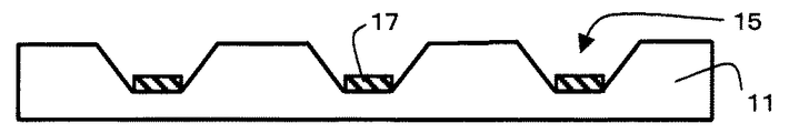
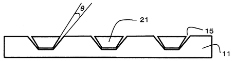
- H01L2924/15153—Shape the die mounting substrate comprising a recess for hosting the device
-
- H—ELECTRICITY
- H01—ELECTRIC ELEMENTS
- H01L—SEMICONDUCTOR DEVICES NOT COVERED BY CLASS H10
- H01L2924/00—Indexing scheme for arrangements or methods for connecting or disconnecting semiconductor or solid-state bodies as covered by H01L24/00
- H01L2924/15—Details of package parts other than the semiconductor or other solid state devices to be connected
- H01L2924/151—Die mounting substrate
- H01L2924/1515—Shape
- H01L2924/15153—Shape the die mounting substrate comprising a recess for hosting the device
- H01L2924/15155—Shape the die mounting substrate comprising a recess for hosting the device the shape of the recess being other than a cuboid
-
- H—ELECTRICITY
- H01—ELECTRIC ELEMENTS
- H01L—SEMICONDUCTOR DEVICES NOT COVERED BY CLASS H10
- H01L2924/00—Indexing scheme for arrangements or methods for connecting or disconnecting semiconductor or solid-state bodies as covered by H01L24/00
- H01L2924/15—Details of package parts other than the semiconductor or other solid state devices to be connected
- H01L2924/151—Die mounting substrate
- H01L2924/15165—Monolayer substrate
Landscapes
- Engineering & Computer Science (AREA)
- Computer Hardware Design (AREA)
- Microelectronics & Electronic Packaging (AREA)
- Power Engineering (AREA)
- Credit Cards Or The Like (AREA)
- Details Of Aerials (AREA)
- Support Of Aerials (AREA)
Priority Applications (1)
| Application Number | Priority Date | Filing Date | Title |
|---|---|---|---|
| JP2002024295A JP3908549B2 (ja) | 2002-01-31 | 2002-01-31 | Rfidタグの製造方法 |
Applications Claiming Priority (1)
| Application Number | Priority Date | Filing Date | Title |
|---|---|---|---|
| JP2002024295A JP3908549B2 (ja) | 2002-01-31 | 2002-01-31 | Rfidタグの製造方法 |
Publications (3)
| Publication Number | Publication Date |
|---|---|
| JP2003223626A JP2003223626A (ja) | 2003-08-08 |
| JP2003223626A5 JP2003223626A5 (enExample) | 2005-08-11 |
| JP3908549B2 true JP3908549B2 (ja) | 2007-04-25 |
Family
ID=27746780
Family Applications (1)
| Application Number | Title | Priority Date | Filing Date |
|---|---|---|---|
| JP2002024295A Expired - Fee Related JP3908549B2 (ja) | 2002-01-31 | 2002-01-31 | Rfidタグの製造方法 |
Country Status (1)
| Country | Link |
|---|---|
| JP (1) | JP3908549B2 (enExample) |
Families Citing this family (27)
| Publication number | Priority date | Publication date | Assignee | Title |
|---|---|---|---|---|
| US6867983B2 (en) | 2002-08-07 | 2005-03-15 | Avery Dennison Corporation | Radio frequency identification device and method |
| JP2006511969A (ja) * | 2002-12-18 | 2006-04-06 | コーニンクレッカ フィリップス エレクトロニクス エヌ ヴィ | 液体の小滴でのマイクロメートル寸法の電子物体の操作 |
| US6940408B2 (en) | 2002-12-31 | 2005-09-06 | Avery Dennison Corporation | RFID device and method of forming |
| US7224280B2 (en) | 2002-12-31 | 2007-05-29 | Avery Dennison Corporation | RFID device and method of forming |
| US20040200061A1 (en) | 2003-04-11 | 2004-10-14 | Coleman James P. | Conductive pattern and method of making |
| US7930815B2 (en) | 2003-04-11 | 2011-04-26 | Avery Dennison Corporation | Conductive pattern and method of making |
| JP4504694B2 (ja) * | 2004-01-30 | 2010-07-14 | トッパン・フォームズ株式会社 | スレッドの製造方法及びicチップ入りシートの製造方法、並びにこれらによって製造されたスレッド及びicチップ入りシート |
| JP2006031336A (ja) * | 2004-07-15 | 2006-02-02 | Fujitsu Ltd | Rfidタグの製造方法 |
| JP4653440B2 (ja) * | 2004-08-13 | 2011-03-16 | 富士通株式会社 | Rfidタグおよびその製造方法 |
| US7202790B2 (en) * | 2004-08-13 | 2007-04-10 | Sensormatic Electronics Corporation | Techniques for tuning an antenna to different operating frequencies |
| US8698262B2 (en) | 2004-09-14 | 2014-04-15 | Semiconductor Energy Laboratory Co., Ltd. | Wireless chip and manufacturing method of the same |
| JP4845461B2 (ja) * | 2004-09-14 | 2011-12-28 | 株式会社半導体エネルギー研究所 | 半導体装置及びその作製方法 |
| JP5057767B2 (ja) * | 2006-01-10 | 2012-10-24 | 株式会社半導体エネルギー研究所 | 半導体装置の作製方法 |
| US20070158804A1 (en) | 2006-01-10 | 2007-07-12 | Semiconductor Energy Laboratory Co., Ltd. | Semiconductor device, manufacturing method of semiconductor device, and RFID tag |
| JP2007274379A (ja) * | 2006-03-31 | 2007-10-18 | Sumitomo Chemical Co Ltd | 無線タグ及びその製造方法 |
| JP2008041005A (ja) * | 2006-08-10 | 2008-02-21 | Hitachi Ltd | Rfidタグおよびその製造方法 |
| EP2567995B1 (en) | 2006-12-26 | 2014-02-19 | Asahi Kasei E-materials Corporation | Resin composition for printing plate |
| TWI423519B (zh) | 2007-09-04 | 2014-01-11 | Mitsubishi Electric Corp | Radio frequency identification tag |
| JP5466381B2 (ja) * | 2008-07-23 | 2014-04-09 | 株式会社沖データ | 媒体搬送装置、印刷媒体、画像形成装置、及び画像形成方法 |
| JP5114357B2 (ja) * | 2008-10-09 | 2013-01-09 | 株式会社日立製作所 | 無線icタグ |
| JP5284858B2 (ja) * | 2009-04-22 | 2013-09-11 | 富士通株式会社 | Rfidタグ |
| WO2011055171A1 (en) * | 2009-11-09 | 2011-05-12 | Time Reversal Communications | Device for receiving and / or emitting electromanetic waves |
| JP2014157180A (ja) * | 2013-02-14 | 2014-08-28 | Ricoh Co Ltd | Rfid粘着感熱ラベル |
| EP2767935A1 (fr) * | 2013-02-18 | 2014-08-20 | NagraID S.A. | Couche plastique pour carte électronique |
| JP6079932B2 (ja) * | 2014-04-28 | 2017-02-15 | 株式会社村田製作所 | 無線icデバイス、クリップ状rfidタグおよびrfidタグ付き物品 |
| JP7312355B2 (ja) * | 2019-03-27 | 2023-07-21 | 大日本印刷株式会社 | Icタグ、icタグの製造方法、及びic保持部の製造方法 |
| CN114729246B (zh) * | 2019-12-23 | 2024-05-28 | 三井化学株式会社 | 电子标签用粘接剂及电子标签 |
-
2002
- 2002-01-31 JP JP2002024295A patent/JP3908549B2/ja not_active Expired - Fee Related
Also Published As
| Publication number | Publication date |
|---|---|
| JP2003223626A (ja) | 2003-08-08 |
Similar Documents
| Publication | Publication Date | Title |
|---|---|---|
| JP3908549B2 (ja) | Rfidタグの製造方法 | |
| JP3998992B2 (ja) | ウェブに実装されたicチップへのアンテナパターン形成方法とicタグ付き包装体 | |
| JP3908514B2 (ja) | Icタグ付き包装体とicタグ付き包装体の製造方法 | |
| JP3894540B2 (ja) | 導電接続部を有するインターポーザ | |
| US7498947B2 (en) | Antenna circuit, IC inlet, multi tag, and method for producing multi tag | |
| JP3854124B2 (ja) | 非接触式icラベル | |
| CN105811085A (zh) | 柔性rfid天线及应用其的pos机装置、电子设备 | |
| JP2008123083A (ja) | 非接触icタグラベルと航空手荷物タグラベル、および非接触icタグラベルの製造方法 | |
| CN106845588B (zh) | 一种耐高温rfid轮胎电子标签及其制作方法 | |
| JP3789827B2 (ja) | Icチップ実装方法とicチップ付き包装体およびicチップ付き包装体の製造方法 | |
| CA2705018C (en) | Rfid tags for pallets and cartons and system for attaching same | |
| CN202854863U (zh) | 电子标签 | |
| JPH11345299A (ja) | 非接触型icカード及びその製造方法 | |
| JP2007042087A (ja) | Rfidタグ及びその製造方法 | |
| CN202632333U (zh) | 一种高频rfid易碎电子标签 | |
| TW202401909A (zh) | 醫療用具用rfid標籤 | |
| CN111126541A (zh) | Rfid智能卡的构造及其制造方法 | |
| CN102955976B (zh) | 一种易碎防伪rfid蚀刻电子标签及其制造工艺 | |
| CN202632328U (zh) | 一种易碎防伪rfid蚀刻电子标签 | |
| CN107451649A (zh) | 电子标签及其制作方法 | |
| CN107766913A (zh) | 一种rfid电子标签制造工艺及rfid电子标签 | |
| JP5375649B2 (ja) | 非接触icラベル | |
| CN207458098U (zh) | 电子标签及射频识别系统 | |
| JP2007076288A (ja) | 導電性パターン形成用金属箔シート | |
| JP2004317544A (ja) | Icチップ実装体付きラベル |
Legal Events
| Date | Code | Title | Description |
|---|---|---|---|
| A521 | Request for written amendment filed |
Free format text: JAPANESE INTERMEDIATE CODE: A523 Effective date: 20050117 |
|
| A621 | Written request for application examination |
Free format text: JAPANESE INTERMEDIATE CODE: A621 Effective date: 20050117 |
|
| A977 | Report on retrieval |
Free format text: JAPANESE INTERMEDIATE CODE: A971007 Effective date: 20060726 |
|
| A131 | Notification of reasons for refusal |
Free format text: JAPANESE INTERMEDIATE CODE: A131 Effective date: 20060905 |
|
| A521 | Request for written amendment filed |
Free format text: JAPANESE INTERMEDIATE CODE: A523 Effective date: 20061023 |
|
| TRDD | Decision of grant or rejection written | ||
| A01 | Written decision to grant a patent or to grant a registration (utility model) |
Free format text: JAPANESE INTERMEDIATE CODE: A01 Effective date: 20070110 |
|
| A61 | First payment of annual fees (during grant procedure) |
Free format text: JAPANESE INTERMEDIATE CODE: A61 Effective date: 20070118 |
|
| R150 | Certificate of patent or registration of utility model |
Free format text: JAPANESE INTERMEDIATE CODE: R150 |
|
| LAPS | Cancellation because of no payment of annual fees |